KR102398125B1 - Imaging element and imaging device - Google Patents
Imaging element and imaging device Download PDFInfo
- Publication number
- KR102398125B1 KR102398125B1 KR1020217006486A KR20217006486A KR102398125B1 KR 102398125 B1 KR102398125 B1 KR 102398125B1 KR 1020217006486 A KR1020217006486 A KR 1020217006486A KR 20217006486 A KR20217006486 A KR 20217006486A KR 102398125 B1 KR102398125 B1 KR 102398125B1
- Authority
- KR
- South Korea
- Prior art keywords
- light
- photoelectric conversion
- unit
- region
- imaging device
- Prior art date
- Legal status (The legal status is an assumption and is not a legal conclusion. Google has not performed a legal analysis and makes no representation as to the accuracy of the status listed.)
- Active
Links
- 238000003384 imaging method Methods 0.000 title claims abstract description 115
- 238000006243 chemical reaction Methods 0.000 claims abstract description 109
- 230000003287 optical effect Effects 0.000 claims abstract description 38
- 238000003860 storage Methods 0.000 claims abstract description 21
- 239000000758 substrate Substances 0.000 claims description 67
- 238000000034 method Methods 0.000 claims description 33
- 230000000903 blocking effect Effects 0.000 claims 3
- 238000009825 accumulation Methods 0.000 abstract description 38
- 230000005540 biological transmission Effects 0.000 abstract description 19
- 102100040678 Programmed cell death protein 1 Human genes 0.000 description 82
- 239000004065 semiconductor Substances 0.000 description 81
- 101710089372 Programmed cell death protein 1 Proteins 0.000 description 78
- 238000009792 diffusion process Methods 0.000 description 17
- 230000008569 process Effects 0.000 description 16
- 238000010586 diagram Methods 0.000 description 15
- 239000013067 intermediate product Substances 0.000 description 13
- 230000000694 effects Effects 0.000 description 12
- XUIMIQQOPSSXEZ-UHFFFAOYSA-N Silicon Chemical compound [Si] XUIMIQQOPSSXEZ-UHFFFAOYSA-N 0.000 description 9
- 229910052710 silicon Inorganic materials 0.000 description 9
- 239000010703 silicon Substances 0.000 description 9
- 230000004048 modification Effects 0.000 description 8
- 238000012986 modification Methods 0.000 description 8
- 230000035945 sensitivity Effects 0.000 description 7
- 230000000875 corresponding effect Effects 0.000 description 6
- 230000012447 hatching Effects 0.000 description 6
- 238000002955 isolation Methods 0.000 description 6
- 229910021420 polycrystalline silicon Inorganic materials 0.000 description 6
- 229920005591 polysilicon Polymers 0.000 description 6
- 239000000463 material Substances 0.000 description 5
- 230000015572 biosynthetic process Effects 0.000 description 4
- 238000004519 manufacturing process Methods 0.000 description 4
- 238000000926 separation method Methods 0.000 description 4
- 206010047571 Visual impairment Diseases 0.000 description 3
- 238000013459 approach Methods 0.000 description 3
- 239000003086 colorant Substances 0.000 description 3
- 230000006866 deterioration Effects 0.000 description 3
- 239000012535 impurity Substances 0.000 description 3
- 108091006146 Channels Proteins 0.000 description 2
- VYPSYNLAJGMNEJ-UHFFFAOYSA-N Silicium dioxide Chemical compound O=[Si]=O VYPSYNLAJGMNEJ-UHFFFAOYSA-N 0.000 description 2
- 239000003990 capacitor Substances 0.000 description 2
- 230000007423 decrease Effects 0.000 description 2
- 238000001514 detection method Methods 0.000 description 2
- 238000005286 illumination Methods 0.000 description 2
- 230000006872 improvement Effects 0.000 description 2
- 239000011159 matrix material Substances 0.000 description 2
- 238000002834 transmittance Methods 0.000 description 2
- 229920000742 Cotton Polymers 0.000 description 1
- 102000004129 N-Type Calcium Channels Human genes 0.000 description 1
- 108090000699 N-Type Calcium Channels Proteins 0.000 description 1
- XAGFODPZIPBFFR-UHFFFAOYSA-N aluminium Chemical compound [Al] XAGFODPZIPBFFR-UHFFFAOYSA-N 0.000 description 1
- 229910052782 aluminium Inorganic materials 0.000 description 1
- 230000003321 amplification Effects 0.000 description 1
- 238000005513 bias potential Methods 0.000 description 1
- 229910052681 coesite Inorganic materials 0.000 description 1
- 230000002596 correlated effect Effects 0.000 description 1
- 229910052906 cristobalite Inorganic materials 0.000 description 1
- 230000002542 deteriorative effect Effects 0.000 description 1
- 230000006870 function Effects 0.000 description 1
- 230000031700 light absorption Effects 0.000 description 1
- 239000007769 metal material Substances 0.000 description 1
- 239000004570 mortar (masonry) Substances 0.000 description 1
- 150000004767 nitrides Chemical class 0.000 description 1
- 238000003199 nucleic acid amplification method Methods 0.000 description 1
- 230000000149 penetrating effect Effects 0.000 description 1
- 238000005036 potential barrier Methods 0.000 description 1
- 238000005070 sampling Methods 0.000 description 1
- 229920006395 saturated elastomer Polymers 0.000 description 1
- 238000004904 shortening Methods 0.000 description 1
- 239000000377 silicon dioxide Substances 0.000 description 1
- 235000012239 silicon dioxide Nutrition 0.000 description 1
- 239000007787 solid Substances 0.000 description 1
- 229910052682 stishovite Inorganic materials 0.000 description 1
- 229910052905 tridymite Inorganic materials 0.000 description 1
- 230000005570 vertical transmission Effects 0.000 description 1
Images


Classifications
-
- H01L27/14627—
-
- H—ELECTRICITY
- H10—SEMICONDUCTOR DEVICES; ELECTRIC SOLID-STATE DEVICES NOT OTHERWISE PROVIDED FOR
- H10F—INORGANIC SEMICONDUCTOR DEVICES SENSITIVE TO INFRARED RADIATION, LIGHT, ELECTROMAGNETIC RADIATION OF SHORTER WAVELENGTH OR CORPUSCULAR RADIATION
- H10F39/00—Integrated devices, or assemblies of multiple devices, comprising at least one element covered by group H10F30/00, e.g. radiation detectors comprising photodiode arrays
- H10F39/80—Constructional details of image sensors
- H10F39/806—Optical elements or arrangements associated with the image sensors
- H10F39/8063—Microlenses
-
- H01L27/14623—
-
- H01L27/14665—
-
- H01L31/0232—
-
- H—ELECTRICITY
- H04—ELECTRIC COMMUNICATION TECHNIQUE
- H04N—PICTORIAL COMMUNICATION, e.g. TELEVISION
- H04N25/00—Circuitry of solid-state image sensors [SSIS]; Control thereof
- H04N25/70—SSIS architectures; Circuits associated therewith
-
- H—ELECTRICITY
- H04—ELECTRIC COMMUNICATION TECHNIQUE
- H04N—PICTORIAL COMMUNICATION, e.g. TELEVISION
- H04N25/00—Circuitry of solid-state image sensors [SSIS]; Control thereof
- H04N25/70—SSIS architectures; Circuits associated therewith
- H04N25/76—Addressed sensors, e.g. MOS or CMOS sensors
-
- H04N5/369—
-
- H04N5/374—
-
- H—ELECTRICITY
- H10—SEMICONDUCTOR DEVICES; ELECTRIC SOLID-STATE DEVICES NOT OTHERWISE PROVIDED FOR
- H10F—INORGANIC SEMICONDUCTOR DEVICES SENSITIVE TO INFRARED RADIATION, LIGHT, ELECTROMAGNETIC RADIATION OF SHORTER WAVELENGTH OR CORPUSCULAR RADIATION
- H10F39/00—Integrated devices, or assemblies of multiple devices, comprising at least one element covered by group H10F30/00, e.g. radiation detectors comprising photodiode arrays
- H10F39/10—Integrated devices
- H10F39/12—Image sensors
- H10F39/18—Complementary metal-oxide-semiconductor [CMOS] image sensors; Photodiode array image sensors
- H10F39/182—Colour image sensors
-
- H—ELECTRICITY
- H10—SEMICONDUCTOR DEVICES; ELECTRIC SOLID-STATE DEVICES NOT OTHERWISE PROVIDED FOR
- H10F—INORGANIC SEMICONDUCTOR DEVICES SENSITIVE TO INFRARED RADIATION, LIGHT, ELECTROMAGNETIC RADIATION OF SHORTER WAVELENGTH OR CORPUSCULAR RADIATION
- H10F39/00—Integrated devices, or assemblies of multiple devices, comprising at least one element covered by group H10F30/00, e.g. radiation detectors comprising photodiode arrays
- H10F39/10—Integrated devices
- H10F39/12—Image sensors
- H10F39/199—Back-illuminated image sensors
-
- H—ELECTRICITY
- H10—SEMICONDUCTOR DEVICES; ELECTRIC SOLID-STATE DEVICES NOT OTHERWISE PROVIDED FOR
- H10F—INORGANIC SEMICONDUCTOR DEVICES SENSITIVE TO INFRARED RADIATION, LIGHT, ELECTROMAGNETIC RADIATION OF SHORTER WAVELENGTH OR CORPUSCULAR RADIATION
- H10F39/00—Integrated devices, or assemblies of multiple devices, comprising at least one element covered by group H10F30/00, e.g. radiation detectors comprising photodiode arrays
- H10F39/80—Constructional details of image sensors
- H10F39/802—Geometry or disposition of elements in pixels, e.g. address-lines or gate electrodes
-
- H—ELECTRICITY
- H10—SEMICONDUCTOR DEVICES; ELECTRIC SOLID-STATE DEVICES NOT OTHERWISE PROVIDED FOR
- H10F—INORGANIC SEMICONDUCTOR DEVICES SENSITIVE TO INFRARED RADIATION, LIGHT, ELECTROMAGNETIC RADIATION OF SHORTER WAVELENGTH OR CORPUSCULAR RADIATION
- H10F39/00—Integrated devices, or assemblies of multiple devices, comprising at least one element covered by group H10F30/00, e.g. radiation detectors comprising photodiode arrays
- H10F39/80—Constructional details of image sensors
- H10F39/805—Coatings
- H10F39/8053—Colour filters
-
- H—ELECTRICITY
- H10—SEMICONDUCTOR DEVICES; ELECTRIC SOLID-STATE DEVICES NOT OTHERWISE PROVIDED FOR
- H10F—INORGANIC SEMICONDUCTOR DEVICES SENSITIVE TO INFRARED RADIATION, LIGHT, ELECTROMAGNETIC RADIATION OF SHORTER WAVELENGTH OR CORPUSCULAR RADIATION
- H10F39/00—Integrated devices, or assemblies of multiple devices, comprising at least one element covered by group H10F30/00, e.g. radiation detectors comprising photodiode arrays
- H10F39/80—Constructional details of image sensors
- H10F39/805—Coatings
- H10F39/8057—Optical shielding
-
- H—ELECTRICITY
- H10—SEMICONDUCTOR DEVICES; ELECTRIC SOLID-STATE DEVICES NOT OTHERWISE PROVIDED FOR
- H10F—INORGANIC SEMICONDUCTOR DEVICES SENSITIVE TO INFRARED RADIATION, LIGHT, ELECTROMAGNETIC RADIATION OF SHORTER WAVELENGTH OR CORPUSCULAR RADIATION
- H10F77/00—Constructional details of devices covered by this subclass
- H10F77/40—Optical elements or arrangements
Landscapes
- Engineering & Computer Science (AREA)
- Multimedia (AREA)
- Signal Processing (AREA)
- Solid State Image Pick-Up Elements (AREA)
- Transforming Light Signals Into Electric Signals (AREA)
- Light Receiving Elements (AREA)
Abstract
촬상 소자는, 마이크로 렌즈를 투과하여 입사된 광을 광전 변환하여 전하를 생성하는 광전 변환부와, 광전 변환부에서 생성된 전하를 축적하는 축적부와, 광전 변환부에서 생성된 전하를 축적부에 전송하는 전송부를 구비하고, 광전 변환부와 전송부와 축적부는, 마이크로 렌즈의 광축 방향을 따라서 형성된다.The imaging device includes a photoelectric conversion unit that photoelectrically converts light incident through the microlens to generate electric charge, an accumulation unit that accumulates charges generated by the photoelectric conversion unit, and an accumulation unit that stores the electric charge generated by the photoelectric conversion unit. A transmission unit for transmitting is provided, wherein the photoelectric conversion unit, the transmission unit, and the storage unit are formed along the optical axis direction of the microlens.
Description
본 발명은 촬상 소자 및 촬상 장치에 관한 것이다.The present invention relates to an image pickup device and an image pickup device.
특허문헌 1 의 공보에는, 다음과 같은 고체 촬상 소자가 개시되어 있다.The following solid-state imaging elements are disclosed by the publication of
반도체 기판에는, 광전 변환부 및 신호 주사 회로부를 포함하고 화소 행렬을 배치하여 이루어지는 촬상 영역이 형성되어 있다. 촬상 영역은, 인접하는 화소와의 경계 부분에 대응하여 각 화소를 둘러싸도록 형성되는 소자 분리 절연막과, 반도체 기판의 표면 상이면서 소자 분리 절연막의 하방 영역에 형성되는 MOSFET 와, 반도체 기판 내의 소자 분리 절연막의 근방 영역에 형성되는 제 1 도전형의 제 1 확산층을 구비한다. 소자 분리 절연막은, 신호 주사 회로부가 형성되는 반도체 기판의 표면으로부터 반도체 기판 중에 오프셋되어 형성되며 또한 반도체 기판의 이면에 도달하여 형성되어 있다. MOSFET 는, 게이트 전극과, 반도체 기판 내이면서 게이트 전극의 상방에 형성되는 제 1 도전형의 제 2 확산층을 구비하고 있다. 제 1 확산층과 제 2 확산층이 접하고, 반도체 기판의 수직 방향에 있어서, 수직 방향과 직교하는 제 1 방향을 따른 제 1 확산층의 폭의 중심은, 제 1 방향을 따른 제 2 확산층의 폭의 중심 근방에 위치한다.In the semiconductor substrate, an imaging region including a photoelectric conversion section and a signal scanning circuit section and by arranging a pixel matrix is formed. The imaging region includes an element isolation insulating film formed to surround each pixel corresponding to a boundary portion with an adjacent pixel, a MOSFET formed on the surface of the semiconductor substrate and in a region below the element isolation insulating film, and an element isolation insulating film in the semiconductor substrate and a first diffusion layer of a first conductivity type formed in a region in the vicinity of The element isolation insulating film is formed offset in the semiconductor substrate from the surface of the semiconductor substrate on which the signal scanning circuit portion is formed, and reaches the back surface of the semiconductor substrate. The MOSFET includes a gate electrode and a second diffusion layer of the first conductivity type formed in the semiconductor substrate and above the gate electrode. The first diffusion layer and the second diffusion layer are in contact, and in the vertical direction of the semiconductor substrate, the center of the width of the first diffusion layer along the first direction orthogonal to the vertical direction is near the center of the width of the second diffusion layer along the first direction is located in
최근, 다화소화의 고체 촬상 소자가 요구되고 있다. 그러나, 종래의 고체 촬상 소자는, 제 1 확산층과 제 2 확산층이 반도체 기판의 표면을 따라 배치되어 있기 때문에, 다화소화하면 수광 면적이 작아진다. 수광 면적이 작아지면, 광전 변환에 의해 발생하는 전하량이 적어져, 감도의 열화가 우려된다.In recent years, a multi-pixel solid-state imaging element is calculated|required. However, in the conventional solid-state imaging device, since the first diffusion layer and the second diffusion layer are arranged along the surface of the semiconductor substrate, the light-receiving area becomes small when multi-pixels are used. When the light-receiving area becomes small, the amount of electric charge generated by photoelectric conversion decreases, and there is a fear of deterioration in sensitivity.
본 발명의 제 1 양태에 의한 촬상 소자는, 마이크로 렌즈를 투과하여 입사된 광을 광전 변환하여 전하를 생성하는 광전 변환부와, 상기 광전 변환부에서 생성된 전하를 축적하는 축적부와, 상기 광전 변환부에서 생성된 전하를 상기 축적부에 전송하는 전송부를 구비한다. 상기 광전 변환부와 상기 전송부와 상기 축적부는, 상기 마이크로 렌즈의 광축 방향을 따라서 형성된다.An image pickup device according to a first aspect of the present invention includes: a photoelectric conversion unit that photoelectrically converts light incident through a microlens to generate an electric charge; an accumulation unit that accumulates charges generated by the photoelectric conversion unit; and a transfer unit for transferring the electric charge generated by the conversion unit to the accumulation unit. The photoelectric conversion unit, the transfer unit, and the accumulation unit are formed along an optical axis direction of the microlens.
본 발명의 제 2 양태에 의한 촬상 소자는, 마이크로 렌즈의 광축과 교차하는 제 1 면과 제 2 면을 갖고, 상기 제 1 면과 상기 제 2 면의 사이에 상기 마이크로 렌즈를 투과하여 입사된 광을 광전 변환하여 전하를 생성하는 광전 변환부와, 상기 광전 변환부에서 생성된 전하를 축적하는 축적부와, 상기 광전 변환부에서 생성된 전하를 상기 축적부에 전송하는 전송부를 구비한다. 상기 마이크로 렌즈의 광축 방향에 있어서, 상기 광전 변환부는 상기 제 1 면측에 형성되고, 상기 축적부는 상기 제 2 면측에 형성되고, 상기 전송부는 상기 광전 변환부와 상기 축적부의 사이에 형성된다.An image pickup device according to a second aspect of the present invention has a first surface and a second surface that intersect an optical axis of a microlens, and light incident through the microlens between the first surface and the second surface A photoelectric conversion unit for generating electric charge by photoelectric conversion, an accumulation unit for accumulating the charge generated by the photoelectric conversion unit, and a transfer unit for transferring the charge generated by the photoelectric conversion unit to the storage unit. In the optical axis direction of the microlens, the photoelectric conversion portion is formed on the first surface side, the accumulation portion is formed on the second surface side, and the transfer portion is formed between the photoelectric conversion portion and the accumulation portion.
본 발명의 제 3 양태에 의한 촬상 장치는, 촬상 소자와, 촬상 소자로부터 출력된 신호에 기초하여 화상 데이터를 생성하는 생성부를 구비한다. 촬상 소자는, 마이크로 렌즈를 투과하여 입사된 광을 광전 변환하여 전하를 생성하는 광전 변환부와, 상기 광전 변환부에서 생성된 전하를 축적하는 축적부와, 상기 광전 변환부에서 생성된 전하를 상기 축적부에 전송하는 전송부를 구비한다. 상기 광전 변환부와 상기 전송부와 상기 축적부는, 상기 마이크로 렌즈의 광축 방향을 따라서 형성된다.An imaging device according to a third aspect of the present invention includes an imaging device and a generating unit that generates image data based on a signal output from the imaging device. The imaging device includes: a photoelectric conversion unit that photoelectrically converts light incident through the microlens to generate electric charge; A transmission unit for transmitting to the storage unit is provided. The photoelectric conversion unit, the transfer unit, and the accumulation unit are formed along an optical axis direction of the microlens.
본 발명의 제 4 양태에 의한 촬상 장치는, 촬상 소자와, 촬상 소자로부터 출력된 신호에 기초하여 화상 데이터를 생성하는 생성부를 구비한다. 촬상 소자는, 마이크로 렌즈의 광축과 교차하는 제 1 면과 제 2 면을 갖고, 상기 제 1 면과 상기 제 2 면의 사이에 상기 마이크로 렌즈를 투과하여 입사된 광을 광전 변환하여 전하를 생성하는 광전 변환부와, 상기 광전 변환부에서 생성된 전하를 축적하는 축적부와, 상기 광전 변환부에서 생성된 전하를 상기 축적부에 전송하는 전송부를 구비한다. 상기 마이크로 렌즈의 광축 방향에 있어서, 상기 광전 변환부는 상기 제 1 면측에 형성되고, 상기 축적부는 상기 제 2 면측에 형성되고, 상기 전송부는 상기 광전 변환부와 상기 축적부의 사이에 형성된다.An imaging device according to a fourth aspect of the present invention includes an imaging device and a generating unit that generates image data based on a signal output from the imaging device. The imaging device has a first surface and a second surface that intersect the optical axis of the microlens, and photoelectric conversion of light incident through the microlens between the first surface and the second surface to generate an electric charge A photoelectric conversion section, an accumulation section for accumulating the electric charge generated by the photoelectric conversion section, and a transfer section for transferring the charge generated by the photoelectric conversion section to the storage section. In the optical axis direction of the microlens, the photoelectric conversion portion is formed on the first surface side, the accumulation portion is formed on the second surface side, and the transfer portion is formed between the photoelectric conversion portion and the accumulation portion.
도 1 은 제 1 실시형태에 의한 고체 촬상 소자 (100) 의 개략 구성을 나타내는 도면.
도 2 는 제 1 실시형태의 화소 (20) 의 등가 회로를 나타내는 도면.
도 3 은 제 1 실시형태의 화소 (20) 의 단면도.
도 4 의 (a) 는 제 1 실시형태의 링상 전송 게이트를 설명하는 횡단면도, (b) 는 배선면측에서 본 배치예를 나타내는 도면, (c) 는 다른 배치예를 나타내는 도면.
도 5 의 (a) 는 제 1 실시형태의 링상 게이트 전극 근방의 상세 구조를 설명하는 단면도, (b) ∼ (d) 는 각각 (a) 의 b-b 선, c-c 선, d-d 선 단면도, (e), (f) 는 전송 게이트 온시에 형성되는 반전층을 설명하는 횡단면도.
도 6 은 제 1 실시형태의 공정을 설명하는 도면.
도 7 은 도 6 에 계속되는 제 1 실시형태의 공정을 설명하는 도면.
도 8 은 도 7 에 계속되는 제 1 실시형태의 공정을 설명하는 도면.
도 9 는 도 8 에 계속되는 제 1 실시형태의 공정을 설명하는 도면.
도 10 은 전송 게이트 전극의 변형예를 설명하는 도 5 에 대응하는 도면.
도 11 은 제 2 실시형태의 화소 (20) 의 단면도.
도 12 는 제 3 실시형태의 화소 (20) 의 단면도.
도 13 의 (a) 는 제 4 실시형태의 화소 (20) 의 단면도, (b) 는 제 5 실시형태의 화소 (20) 의 단면도.
도 14 의 (a) 는 제 6 실시형태의 화소 (20) 의 단면도, (b) 는 제 7 실시형태의 화소 (20) 의 단면도.
도 15 는 제 4 실시형태의 변형예의 화소 (20) 의 단면도.
도 16 의 (a) 는 제 8 실시형태의 화소 (20) 의 단면도, (b) 는 제 9 실시형태의 화소 (20) 의 단면도.
도 17 의 (a) 는 제 10 실시형태의 화소 (20) 의 단면도, (b) 는 제 11 실시형태의 화소 (20) 의 단면도.
도 18 은 본 발명의 촬상 장치를 설명하는 블록도.BRIEF DESCRIPTION OF THE DRAWINGS Fig. 1 is a diagram showing a schematic configuration of a solid-
Fig. 2 is a diagram showing an equivalent circuit of the pixel 20 of the first embodiment;
Fig. 3 is a cross-sectional view of the pixel 20 of the first embodiment.
Fig. 4 (a) is a cross-sectional view for explaining the ring-shaped transfer gate according to the first embodiment, (b) is a view showing an arrangement example seen from the wiring surface side, (c) is a view showing another arrangement example;
Fig. 5 (a) is a sectional view for explaining a detailed structure in the vicinity of the ring-shaped gate electrode of the first embodiment, (b) to (d) are sectional views along the bb, cc, and dd lines of (a), respectively, (e) , (f) is a cross-sectional view illustrating the inversion layer formed when the transfer gate is on.
It is a figure explaining the process of 1st Embodiment.
Fig. 7 is a view for explaining a process of the first embodiment following Fig. 6;
Fig. 8 is a view for explaining a process of the first embodiment following Fig. 7;
Fig. 9 is a view for explaining a process of the first embodiment following Fig. 8;
Fig. 10 is a view corresponding to Fig. 5 for explaining a modified example of a transfer gate electrode;
11 is a cross-sectional view of a pixel 20 in the second embodiment.
Fig. 12 is a cross-sectional view of a pixel 20 in the third embodiment.
Fig. 13 (a) is a cross-sectional view of the pixel 20 of the fourth embodiment, and (b) is a cross-sectional view of the pixel 20 of the fifth embodiment.
Fig. 14 (a) is a cross-sectional view of the pixel 20 of the sixth embodiment, and (b) is a cross-sectional view of the pixel 20 of the seventh embodiment.
Fig. 15 is a cross-sectional view of a pixel 20 of a modification of the fourth embodiment.
Fig. 16 (a) is a cross-sectional view of a pixel 20 of an eighth embodiment, and (b) is a cross-sectional view of a pixel 20 of a ninth embodiment.
Fig. 17 (a) is a cross-sectional view of a pixel 20 of a tenth embodiment, and (b) is a cross-sectional view of a pixel 20 of an eleventh embodiment.
Fig. 18 is a block diagram for explaining an imaging device of the present invention;
《제 1 실시형태》 《First embodiment》
(소자 개략 구성) (Device outline configuration)
도 1 은, 본 실시형태의 고체 촬상 소자 (100) 의 개략 구성을 나타내는 도면이다.1 : is a figure which shows the schematic structure of the solid-
고체 촬상 소자 (100) 는, 수광면 (입사면) 에 화소 (20) 를 화소 배열한 촬상부 (30) 를 구비한다. 이들 화소 (20) 에는, 수직 제어선 (32) 을 통해서, 수직 주사 회로 (31) 으로부터 구동 신호가 공급된다. 또, 화소 (20) 는, 열 단위로 수직 신호선 (21) 에 접속된다. 이 수직 신호선 (21) 은 화소 전류원 (22) 에 각각 접속된다.The solid-
한편, 화소 (20) 로부터 수직 신호선 (21) 에 대해 시분할로 출력되는 노이즈 출력과 신호 출력은, 열 앰프 (23) 을 통하여, CDS 회로 (24) (상관 이중 샘플링 회로) 에 순차적으로 입력된다. 이 CDS 회로 (24) 는, 양 출력의 차분을 취해 진정한 신호 출력을 생성한다. 이 진정한 신호 출력은, 수평 주사 회로 (33) 로부터의 구동 신호에 의해 수평 주사되어, 수평 신호선 (25) 에 순차 출력된다. 이 수평 신호선 (25) 의 신호 출력은, 출력 앰프 (26) 를 통해서 출력 단자 (27) 에 출력한다.On the other hand, the noise output and signal output output in time division from the pixel 20 to the vertical signal line 21 are sequentially input to the CDS circuit 24 (correlated double sampling circuit) via the column amplifier 23 . This
(화소 (20) 의 등가 회로) (equivalent circuit of pixel 20)
도 2 는, 상기 서술한 화소 (20) 의 등가 회로를 나타내는 도면이다.FIG. 2 is a diagram showing an equivalent circuit of the pixel 20 described above.
화소 (20) 에는, 포토다이오드 (PD (1)) 가 형성된다. PD (1) 는, 전송 구동 신호 (전송 게이트 전압) 에 의해 게이트 제어되는 전송 트랜지스터 (TG : 이하로 전송 게이트라고도 부른다) (4) 를 통하여 플로팅 디퓨전 (FD) (8) 에 접속된다. FD (8) 는, 증폭 트랜지스터 (AMP) (11) 의 게이트 전극에 접속된다. 또, FD (8) 는, 리셋 구동 신호 (리셋 게이트 전압) 에 의해 게이트 제어되는 리셋 트랜지스터 (RST : 이하에서 리셋 게이트라고도 부른다) (13) 를 통하여 기준 전위 (Vdd) 에 접속된다. 증폭 트랜지스터 (11) 는, 드레인이 전위 (Vdd) 에 접속되고, 소스가 선택 구동 신호 (선택 게이트 전압) 에 의해 게이트 제어되는 선택 트랜지스터 (SEL : 이하로 선택 게이트라고도 부른다) (12) 를 통하여 수직 신호선 (21) 에 접속된다.A photodiode PD ( 1 ) is formed in the pixel 20 . The
전송 트랜지스터 (4) 의 전송 게이트 전압은 전송 배선 (4H) 을 통하여 공급된다. 리셋 트랜지스터 (13) 의 리셋 게이트 전압은 리셋 배선 (13H) 을 통하여 공급된다. 선택 트랜지스터 (12) 의 선택 게이트 전압은 선택 배선 (12H) 을 통하여 공급된다. 전송 배선 (4H), 리셋 배선 (13H) 및 선택 배선 (12H) 은, PD (1) 나 FD (8) 가 형성되는 기판과 동일한 기판 내의 배선 영역 (203) (배선층) 에 형성된다.The transfer gate voltage of the transfer transistor 4 is supplied through the
그 밖의 구성은 도 1 과 같기 때문에, 여기서의 중복 설명을 생략한다.Since the rest of the configuration is the same as in FIG. 1 , the redundant description here is omitted.
(화소 (20) 의 소자 구조) (Element structure of pixel 20)
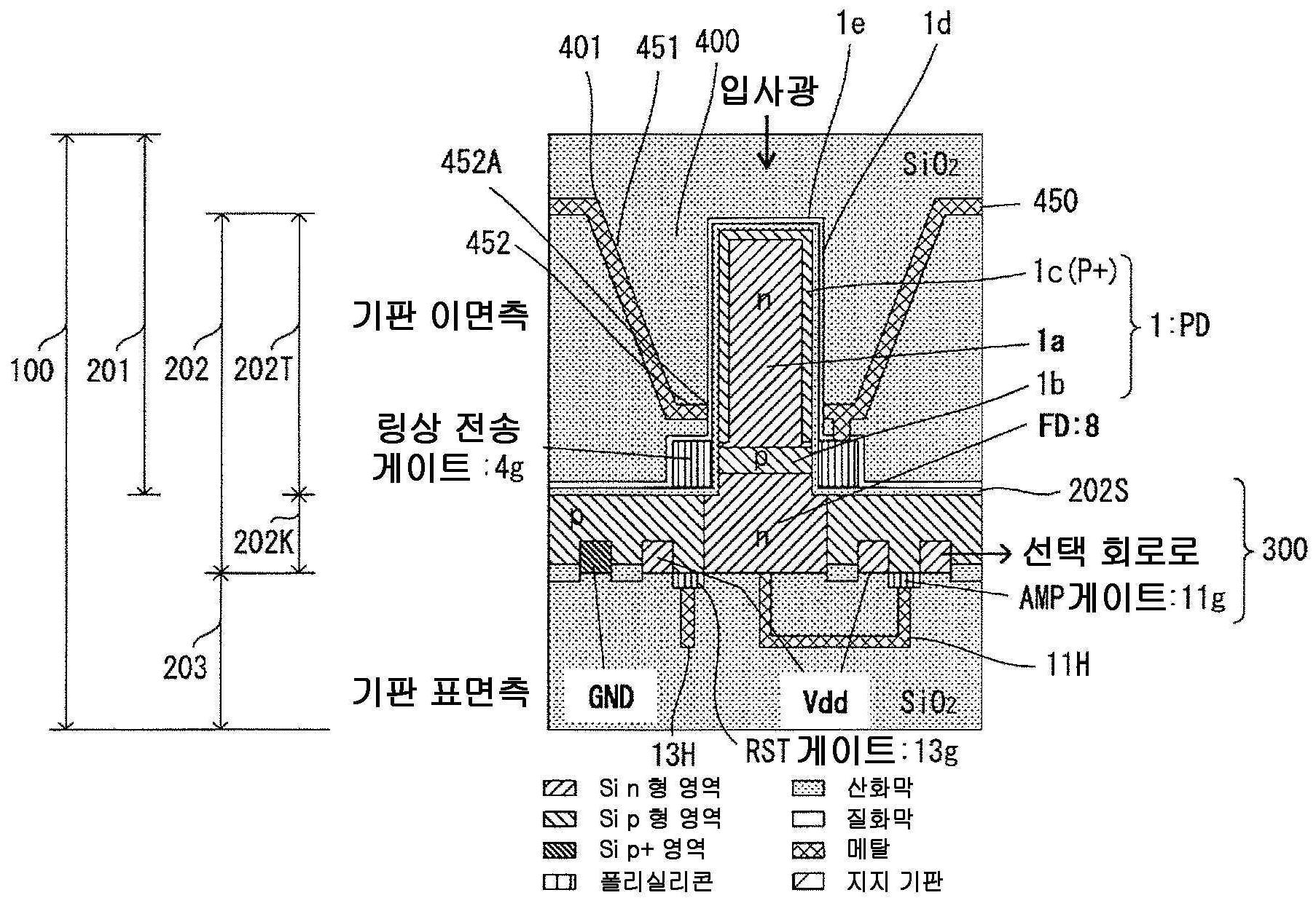
도 3 은, 화소 (20) 의 소자 구조의 일부를 나타내는 단면도이다. 입사광은, 도 3 의 상방으로부터 입사된다.3 is a cross-sectional view showing a part of the element structure of the pixel 20 . Incident light is incident from above in FIG. 3 .
고체 촬상 소자 (100) 는 반도체 기판 (200) 에 형성된다. 반도체 기판 (200) 은 모놀리식 반도체 기판이다. 반도체 기판 (200) 은, 도 3 의 상방 (수광면측) 으로부터 하방 (배선 영역측) 을 향해 적층되는 개략 3 개의 층으로 구성된다. 최상방에는 산화막 (201), 최하방에는 배선 영역 (203), 산화막 (201) 과 배선 영역 (203) 의 사이에는 확산 영역 (202) 이 형성된다. 또한, 확산 영역 (202) 을 반도체 영역이라고 부른다. 배선 영역 (203) 은 배선 이외의 영역이 산화층이다. 또한, 산화막 및 산화층은, 주로 반도체 기판을 산화한 영역으로 이루어지는 막 및 층이다.The solid-
(반도체 영역 (202)) (Semiconductor area 202)
반도체 기판 (200) 의 반도체 영역 (확산 영역) (202) 에는, 기판 두께 방향 (광이 입사되는 방향) 으로 긴, 세로로 긴 형상의 PD (1) 와, 기판의 면 방향으로 배치 형성되는 신호 판독 출력 회로 (300) 가 형성되어 있다. 반도체 영역 (202) 은, 얇은 층 형상의 기부 영역 (202K) 과, 기부 영역 (202K) 으로부터 광이 입사되는 수광면측으로 연장되는 볼록 영역 (202T) 을 갖는다. 볼록 영역 (202T) 에는 PD (1) 가 형성되고, 기부 영역 (202K) 에는 신호 판독 출력 회로 (300) 가 형성되어 있다. PD (1) 나 신호 판독 출력 회로 (300) 는, p 형 영역의 소정 지점에 p 형 불순물과 n 형 불순물을 적절한 농도로 선택적으로 주입함으로써 형성된다. In the semiconductor region (diffusion region) 202 of the
반도체 영역 (202) 에는, 입사된 광을 광전 변환에 의해 전하로 변환하는 PD (1) 와, PD (1) 에서 광전 변환된 전하를 화소 신호로서 수직 신호선 (21) 에 출력하기 위한 신호 판독 출력 회로 (300) 가 형성된다.In the
반도체 영역 (202) 에 형성되는 신호 판독 출력 회로 (300) 는, PD (1) 의 전하를 FD (8) 로 전송하는 전송 트랜지스터 (4) 와, 전송된 전하를 축적하여 전압으로 변환하는 FD (8) 와, FD (8) 의 출력 전압을 증폭하는 증폭 트랜지스터 (11) 와, FD (8) 를 리셋하는 리셋 트랜지스터 (13) 를 포함하여 구성된다.The
전송 트랜지스터 (4) 는, 게이트 전극 (4g) 에 게이트 전압이 인가되면, PD (1) 에서 발생한 전하를 FD (8) 로 전송한다. 전송 게이트 전극 (4g) 은, PD (1) 의 외주의 산화막 (201) 에 형성된 링상의 전극이다. 전송 게이트 전극 (4g) 과 반도체 영역 (202) 의 사이에는 절연막 (202S) (산화막) 이 형성되어 있다. 링상의 전송 게이트 전극 (4g) 은 후술한다. The transfer transistor 4 transfers the electric charge generated in the
전송 트랜지스터 (4) 는, 게이트 전극 (4g) 에 게이트 전압이 인가되었을 때, PD (1) 에서 광전 변환된 전하를 FD (8) 로 전송하는 전송로 (채널) 가 p-n 접합부에 형성되는 트랜지스터이다. 전송로가 되는 p 영역 (1b) 는, 광이 입사되는 방향에 있어서 PD (1) 와 FD (8) 의 사이에 배치된다. 바꾸어 말하면, 광이 입사되는 수광면측으로부터 배선 영역측을 향해, PD (1) 와 p 영역 (1b) 과 FD (8) 가 배치되어 있다.The transfer transistor 4 is a transistor in which a transfer path (channel) for transferring the charges photoelectrically converted from the
FD (8) 는, 전송 트랜지스터 (4) 로부터 전송되는 전하를 축적하여 전압으로 변환하는 커패시터로, PD (1) 의 아래의 반도체 기판 기부 영역 (202K) 에 형성되어 있다. 광전 변환에 의해 발생한 전하는 FD (8) 의 커패시터에 의해 전압으로 변환되고, 이 전압이 증폭 트랜지스터 (11) 의 게이트 전압이 된다. PD (1) 에서 발생한 전하 (Q) 를 FD (8) 의 용량 (C) 으로 나눈 값이 화소 (20) 의 화소 신호의 기초이기 때문에, FD (8) 의 용량을 작게 하는 것이 촬상 소자의 감도 향상에 기여한다.The
증폭 트랜지스터 (11) 는, 게이트 전극 (11g) 에 인가되는 FD (8) 의 전압을 증폭시킨다. 증폭 트랜지스터 (11) 에 의해 증폭된 전압이, 도시하지 않은 적층되는 다른 반도체 기판의 선택 회로에 출력된다.The amplifying transistor 11 amplifies the voltage of the
또한, 도시하지 않은 반도체 기판에 형성되는 선택 회로는, 증폭 트랜지스터 (11) 로부터 출력되는 화소 신호를 수직 신호선 (21) 에 출력하는 선택 트랜지스터 (12) 를 포함한다.In addition, the selection circuit formed on the semiconductor substrate (not shown) includes the selection transistor 12 for outputting the pixel signal output from the amplifying transistor 11 to the vertical signal line 21 .
리셋 트랜지스터 (13) 는, 게이트 전극 (13g) 에 게이트 전압이 인가되면, FD (8) 에 축적된 전하를 배출하여 기준 전위 (Vdd) 로 리셋한다.When a gate voltage is applied to the
(링상 전송 게이트 전극 (4g)) (ring-shaped transfer gate electrode (4g))
도 4(a) 는, 전송 게이트 전극 (4g) 의 형상을 설명하는 도면으로서, 수광면측에서 화소 (20) 의 내부 구조를 본 모식도이다. 우하향의 해칭선은 p 영역, 세로의 해칭선은 폴리실리콘 영역이다. 도 4(a) 의 전송 게이트 전극 (4g) 은, p 영역 (도 3 의 1b) 의 주위를 둘러싸도록 배치되어 있다. 광이 입사되는 방향과 교차하는 방향에 있어서, 전송로가 되는 p 영역이 전송 게이트 전극 (4g) 의 사이에 있다. 전송 게이트 전극 (4g) 과 p 영역의 사이에는 절연막 (202S) 이 있다.Fig. 4(a) is a diagram for explaining the shape of the
PD (1) 는, p 형 반도체 영역 (202) 의 기부 영역 (202K) 으로부터 수광면을 향해 돌출되어 있다. 각기둥 형상의 PD (1) 의 주위에는, 폴리실리콘에 의해 전송 게이트 전극 (4g) 이 링상으로 형성되어 있다.The
도 5 를 참조하여 PD (1) 와 게이트 전극 (4g) 의 전기적 접속 관계를 설명한다.An electrical connection relationship between the
(a) 의 b-b 단면을 (b) 에 나타내고, (a) 의 c-c 단면을 (c) 에 나타내고, (a) 의 d-d 단면을 (d) 에 나타낸다. 게이트 전극 (4g) 에 전압이 인가되었을 때, PD (1) 의 p 형 광전 변환 영역 (1c) 이 p 형 반도체 영역 (1b) 에 접속하도록 형성되어 있다. 즉, 게이트 전극에 전압이 인가되었을 때, c-c 단면에서는, p 형 광전 변환 영역 (1c) 의 외주 전체 둘레에 반전층이 형성되지만, (e) 에 나타내는 바와 같이, b-b 단면에서는, n 형 광전 변환 영역 (1a) 의 안쪽에 p 형 영역이 잔존된다. 이 p 형 영역의 잔존에 의해, 전송 게이트 전극에 게이트 전압이 인가되었을 때 p 형 영역 (1b, 1c) 이 GND 전위로 고정된다. The b-b section of (a) is shown in (b), the c-c section of (a) is shown in (c), and the d-d section of (a) is shown in (d). When a voltage is applied to the
도 5 (b), (d) 로부터 알 수 있듯이, 게이트 전극 (4g) 에 전압이 인가되어 있지 않을 때에도, p 형 광전 변환 영역 (1c) 이 p 형 반도체 영역 (1b) 에 접속하도록 형성되어 있다.5(b) and (d), even when no voltage is applied to the
도 4(b) 는, p 형 반도체 영역 (202) 의 기부 영역 (202K) 에 형성한 신호 판독 출력 회로 (300) 의 배치예를 배선면측에서 보아 나타낸 모식도이다. 좌하향의 해칭선은 n 영역, 세로의 해칭선은 폴리실리콘 영역, 점묘화 영역은 산화막이다. Fig. 4(b) is a schematic diagram showing an arrangement example of the
리셋 게이트 전극 (13g) 은, 리셋 게이트 전극 (13g) 에 게이트 전압이 인가되면, FD (8) 에 축적된 전하를 배출하여 기준 전위 (Vdd) 로 리셋한다. 증폭 트랜지스터 (11) 는, 게이트 전극 (11g) 에 인가되는 FD (8) 의 전압에 기초하여 제어되고, FD (8) 의 전압을 증폭시킨다. GND 단자는, p 형 반도체 영역 (202) 을 GND 전위로 하기 위한 단자이다. 또한, 신호 판독 출력 회로 (300) 에 화소 신호를 출력하기 위한 선택 트랜지스터가 배치되어 있어도 된다.When a gate voltage is applied to the
도 4(c) 는, p 형 반도체 영역 (202) 의 기부 영역 (202K) 에 형성한 신호 판독 출력 회로 (300) 의 다른 배치예를 나타내는 모식도이다. 좌하향의 해칭선은 n 영역, 세로의 해칭선은 폴리실리콘 영역, 점묘화 영역은 산화막이다.4C is a schematic diagram showing another arrangement example of the
리셋 게이트 전극 (13g) 은, 리셋 게이트 전극 (13g) 에 게이트 전압이 인가되면 FD (8) 를 기준 전위 (Vdd) 로 리셋한다. 증폭 트랜지스터 (11) 는, 게이트 전극 (11g) 에 인가되는 FD (8) 의 전압에 기초하여 제어되고, FD (8) 의 전압을 증폭시킨다. GND 단자는, p 형 반도체 영역 (202) 을 GND 전위로 하기 위한 단자이다.The
(배선 영역 (203)) (Wiring Area 203)
도 3 으로 돌아와 설명한다. 배선 영역 (203) 에는, 상기 서술한 FD (8) 와 증폭 트랜지스터 (11) 의 게이트 전극 (11g) 을 접속하는 배선 (11H) 과, 리셋 트랜지스터 (13) 의 게이트 전극 (13g) 에 게이트 전압을 공급하는 리셋 배선 (13H) 이 형성되어 있다.Returning to FIG. 3, description will be made. In the
(산화막 (201)) (Oxide film (201))
산화막 (201) 의 표면, 즉 반도체 기판 (200) 의 이면인 수광면 (입사면) 에는 차광막 (450) 이 형성되어 있다. 차광막 (450) 은, 신호 판독 출력 회로 (300) 등에 광이 입사되는 것을 방지하기 위해 형성된다. 차광막 (450) 은, PD (1) 로의 광 입사에 제공되는 지점에 있어서, 수광면으로부터 우묵하게 패인 막자사발 형상의 광입사 영역 (400) 을 형성하는 각뿔부 (451) 를 구비하고 있다. PD (1) 는 광입사 영역 (400) 의 저부 (底部) 에 있어서 각뿔부 (451) 를 관통하여 수광면측으로 연장되어 있다. 광입사 영역 (400) 의 수광면에서의 넓이, 즉, 각뿔부 (451) 의 수광면측 단 (端) 의 윤곽이 촬상 소자 (100) 의 개구 (401) 가 된다. 차광막 (450) 은, 광입사 영역 (400) 에 입사되는 광이 신호 판독 출력 회로 (300) 등으로 입사되는 것을 방지한다. 차광막 (450) 은, 반도체 영역 (202) 의 적어도 일부를 차광한다. 또, 차광막 (450) 은, 전송 게이트 (4g) 에 게이트 전압을 제공하는 전송 배선 (도 2 에 부호 4H 로 나타내고 있다) 의 기능도 갖는다. 이 점은 나중에 설명한다.A light-shielding
(PD (1) 의 상세) (Details of PD (1))
도 3 을 참조하여 PD (1) 를 상세하게 설명한다.The
PD (1) 는, n 형 불순물을 p 형 반도체 영역 (202) 의 소정 영역에 선택적으로 주입하여 형성한 p-n 접합의 광전 변환부이다. PD (1) 는 각기둥 형상으로 형성되어 있다. 각기둥의 안쪽에는 n 형 광전 변환 영역 (1a) 이 형성되고, n 형 광전 변환 영역 (1a) 의 하방에 접하는 지점에는 p 형 광전 변환 영역 (1b) 이 형성되고, n 형 광전 변환 영역 (1a) 의 표면에는 p+ 영역 (1c) 이 형성되어 있다. n 형 광전 변환 영역 (1a) 과 p 형 광전 변환 영역 (1b) 에 의해 p-n 접합의 광전 변환부를 형성하고 있다. 또한, PD (1) 는 각기둥 형상에 한정되지 않고, 광이 입사되는 방향으로 신장된 입체이면 된다. 예를 들어, 원기둥, 타원기둥, 각뿔, 원뿔, 타원뿔, 구체, 타원체, 다면체 등이어도 된다.The
PD (1) 의 표면 영역 (1c) 의 p+ 영역은, 광전 변환 영역 (1a) 의 공핍층이 표면에 도달하는 것을 방지한다. 공핍층이 표면에 도달하는 것이 방지되므로, 반도체 계면에서 발생하는 암전류가 광전 변환 영역 (1a) 으로 흘러드는 것을 방지한다.The p+ region of the
p 형 광전 변환 영역 (1b) 의 하방에 접하도록 n 형 전하 축적 영역 (8) 이 형성된다. 편의상, 이 n 형 전하 축적 영역을 FD (8) 로서 설명한다. The n-type
전송 트랜지스터 (4) 의 게이트 전극 (4g) 에 게이트 전압이 인가되면, p 형 광전 변환 영역 (1b) 표면에 반전층인 n 형의 채널이 생긴다. 이 채널을 전류가 흘러서 FD (8) 에 전하가 축적된다.When a gate voltage is applied to the
PD (1) 는, 신호 판독 출력 회로 (300) 가 형성되는 반도체 영역 (202) 으로부터 수광면측으로 돌출하여 형성되어 있다. 바꾸어 말하면, PD (1) 는, 신호 판독 출력 회로 (300) 가 형성되어 있는 반도체 영역 (202) 의 기부 영역 (202K) 으로부터 수광면측으로 연장되어 돌출되는 볼록 영역 (202T) 에 형성되어 있다. 즉, 도 3 에 있어서, PD (1) 는, 신호 판독 출력 회로 (300) 가 형성되는 기부 영역 (202K) 으로부터 수광면측으로 연장되는 볼록 형상이다. 바꾸어 말하면, PD (1) 의 적어도 일부는, 광이 입사되는 방향을 따라 연장되는 볼록부를 가지고 있다. PD (1) 의 적어도 일부는, 후술하는 차광막 저부 (452) 가 갖는 개구부 (452A) 보다도 광이 입사되는 방향을 향해 연장되어 있고, 차광부 (452) 보다 수광면측에 있다. 또한, PD (1) 의 적어도 일부는, 반사막 (450) 또는 개구 (401) 보다도 광이 입사되는 방향을 향해 연장되어 있어도 된다.The
또한, 볼록 형상의 PD (1) 의 연장 방향은 도시하지 않은 마이크로 렌즈의 광축 방향이다. 광이 입사되는 방향도 마이크로 렌즈의 광축 방향이다.In addition, the extending direction of the convex-shaped
반도체 영역 (202) 의 볼록 영역 (202T) 은, 수광면측의 산화막 (201) 에 형성되어 있는 막자사발상 오목부에 기판 표면측으로부터 돌출되어 있다. 막자사발상의 오목부 형상을 규정하는 면에는 차광막 (450) 이 형성되어 있다. 오목부의 차광막 (450) 은 상기 서술한 각뿔부 (451) 이고, 각뿔부 (451) 의 상면에는, 바꾸어 말하면 오목부에는 산화층이 퇴적되어 있다. 오목부가 광로 영역 (400) 으로서 이용된다. 광로 영역 (400) 에 입사된 광은 차광막 (450) 의 각뿔부 (451) 에서 반사되어 PD (1) 의 측면 (1d) 으로부터 입사된다. A
광로 영역 (400) 에는 산화막, 예를 들어 산화층이 퇴적되어 있다고 설명했지만, 가시광 성분의 투과율이 소정 이상이면, 광로 영역 (400) 내부의 재질은 산화층으로 한정되지 않는다.Although it has been explained that an oxide film, for example, an oxide layer is deposited in the
광로 영역 (400) 내부를 공동 (空洞) 으로 해도 된다. 광로 영역 (400) 의 형상은 사각형에 한정되지 않는다. 예를 들어, 광로 영역 (400) 의 형상은, 원, 타원, 다각형, 원환이어도 된다.It is good also considering the inside of the optical path area|
차광막 (450) 은, 각뿔부 (451) 의 최하단에서 수광면과 평행하게 형성된 저부 (452) 를 구비하고 있다. PD (1) 가 형성된 반도체 영역 (202) 의 볼록 영역 (202T) 은, 이 저부 (452) 를 관통하여, 즉 저부 (452) 에 형성한 개구부 (452A) 를 통하여 수광면을 향해 연장되어 있다. 광로 영역 (400) 에 입사된 광은 차광막 (450) 의 저부의 차광막 (452) 에 의해 차광되어, 산화막 (201) 하방의 반도체 영역 (202) 으로 광이 입사되는 것을 방지한다.The light-shielding
바꾸어 말하면, 광로 영역 (400) 의 내주 경사면에는 반사막 (451) 이 형성되고, 광로 영역 (400) 의 저부에는 차광막 (452) 이 형성되어 있다. 반사막 (451) 및 차광막 (452) 은, 예를 들어 반사율이 높은 알루미늄 등을 PVD 로 형성할 수 있다. 반사막 (451) 은 반사율이 높은 재료, 차광막 (452) 은 광 투과율이 낮은 재료로 형성되면 되며, 동일한 재료여도 되고, 상이한 재료여도 된다.In other words, the
광로 영역 (400) 의 상면에는, 컬러 필터와 마이크로 렌즈가 형성되어 있다. 컬러 필터를 생략할 수도 있다.A color filter and a microlens are formed on the upper surface of the
이상 설명한 고체 촬상 소자 (100) 에 의한 광전 변환 동작을 설명한다.The photoelectric conversion operation|movement by the solid-
고체 촬상 소자 (100) 의 수광면에는 매트릭스상으로 화소가 배열되어 있다. 촬상 소자 (100) 에 도달한 광은, 화소마다 형성되어 있는 마이크로 렌즈에 의해 집광된다. 집광된 광은 컬러 필터에 의해 파장 선택되어 개구 (401) 로부터 광로 영역 (400) 에 입사된다. 입사광의 일부는 PD (1) 의 면 (1e) 으로부터 내부로 입사된다. 광로 영역 (400) 에 입사된 광 중 면 (1e) 으로부터 PD (1) 에 입사된 광 이외의 광, 즉 PD (1) 의 외측면 (1d) 과 반사막 (차광막 (450) 의 각뿔부) (451) 의 사이의 광로 영역 (400) 에 입사된 광은, 반사막 (451) 에서 반사되어 PD (1) 에 측면 (1d) 으로부터 입사된다. PD (1) 는, 면 (1e) 과 측면 (1d) 으로부터 입사되는 광을 전하로 광전 변환한다. 이로써, PD (1) 는 입사된 광으로부터 보다 효율적으로 전하를 발생시킨다.Pixels are arranged in a matrix on the light-receiving surface of the solid-
광로 영역 (400) 의 저부에 입사되는 광은 차광막 (452) 에 의해 차광된다. 차광막 (452) 은, 입사광이 신호 판독 출력 회로 (300) 가 형성되어 있는 반도체 영역 (202) 에 입사되는 것을 방지한다. 이로써, 판독 출력 회로 (300) 에 입사된 광에 의한 노이즈의 발생을 저감할 수 있다. 차광막 (452) 은, 상기 서술한 바와 같이 PD (1) 가 볼록 형상이기 때문에, PD (1) 가 광이 입사되는 방향을 향해 연장되는 부분에 개구부 (452A) 를 갖는다.Light incident on the bottom of the
전송 트랜지스터 (4) 와 리셋 트랜지스터 (13) 에 의해 PD (1) 와 FD (8) 를 리셋하고 나서 소정의 축적 시간이 경과한 시점에서 전송 트랜지스터 (4) 를 온하면, PD (1) 에 축적된 전하에 의한 검출 전류에 의해 FD (8) 에 전하가 축적된다. FD (8) 에 축적된 전하는 전압으로 변환되어 증폭 트랜지스터 (11) 의 게이트 전극에 인가되어 증폭된다. 증폭된 전압은 도시하지 않은 기판에 형성된 선택 트랜지스터 (12) 로부터 화소 신호로서 선택되어 수직 신호선 (21) 에 출력된다.When the transfer transistor 4 is turned on when a predetermined accumulation time has elapsed after the
PD (1) 로부터 FD (8) 로의 검출 전류는, 반도체 기판의 두께 방향으로 흐른다. 즉, 수직 전송된다.The detection current from the PD ( 1 ) to the FD ( 8 ) flows in the thickness direction of the semiconductor substrate. That is, it is transmitted vertically.
특허문헌 1 의 고체 촬상 소자에 있어서, 전하를 화소 신호로서 취출하는 신호 판독 출력 회로 (300) 는, 전송 회로와 증폭 회로와 선택 회로의 사이에서 신호를 반도체 기판 표면을 따라 전송한다.In the solid-state imaging device of
제 1 실시형태의 고체 촬상 소자 (1) 에서는, PD (1) 로부터 FD (8) 까지의 신호 경로가 기판 두께 방향이 되어, 그 만큼, 전송 트랜지스터 (4) 의 기판 표면 방향의 크기를 작게 할 수 있다. 즉, 화소의 소형화를 도모할 수 있다.In the solid-
이상 설명한 제 1 실시형태에 의한 고체 촬상 소자의 작용 효과는 다음과 같다. The effects of the solid-state imaging device according to the first embodiment described above are as follows.
(1) 고체 촬상 소자 (100) 는, 입사된 광을 광전 변환하여 전하를 생성하는 PD (광전 변환 영역) (1) 와, PD (1) 로부터 전하가 전송되는 FD (전하 전송 영역) (8) 를 포함하는 판독 출력 회로 (300) 가 형성된 반도체 영역 (202) 을 구비한다. 반도체 영역 (202), 즉 PD (1) 의 적어도 일부는, 수광면측에 형성한 광로 영역 (입사 영역) (400) 으로 돌출하여 형성되어 있다. (1) The solid-
이와 같은 PD (1) 의 구성에 의해, 입사광이 PD (1) 의 면 (1e) 과 측면 (1d) 으로부터 입사되므로, PD (1) 의 수광 면적이 커진다. 따라서, S/N 비가 커져, 감도가 향상된다. 또, 노출 시간의 단축에 의한 S/N 비의 열화, 화소의 미소화에 수반되는 S/N 비의 열화를 방지할 수 있다. 따라서, 예를 들어 1000 ∼ 10000 프레임과 같은 고속 판독 출력되는 고체 촬상 소자라도 노이즈가 적은 고화질의 화상을 얻을 수 있다.With such a configuration of the
(2) PD (1) 는 광로 영역 (400) 의 저부를 관통하여 수광면측까지 연장되어 있다. PD (1) 의 측면 (1d) 으로부터 입사되는 광의 일부가, PD (1) 의 측면 (1d) 을 따라 광로 영역 안에서 하방으로 입사되고, 수광면측으로부터 판독 출력 회로 (300) 가 형성되어 있는 반도체 영역 (202) 에 광이 입사되지 않도록, 광로 영역 (400) 의 저부에는 차광막 (452) 이 형성되어 있다.(2) The
그 때문에, PD (1) 의 측면으로부터의 광의 입사를 가능하게 한 구성을 채용해도, 판독 출력 회로 (300) 로의 광의 입사가 저감되어, 노이즈의 발생을 억제할 수 있다.Therefore, even if a configuration that enables light to enter from the side of the
(3) n 형 영역 (1a) 과 p 형 영역 (1b) 과 p+ 영역 (1c) 을 포함하는 PD (1) 는, FD (8) 를 포함하는 판독 출력 회로 (300) 의 형성면보다 수광면측으로 연장되어 있다. FD (8) 는 p 형 영역 (1b) 의 바로 아래에 접하고 있다. 그 때문에, PD (1) 에서 발생한 전하는, PD (1) 로부터 FD (8) 로 수직 전송된다. 즉, 반도체 기판의 면에 평행한 횡전송 방식이 아니라, 반도체 기판 두께 방향의 신호 경로에 의해 전하의 전송이 이루어진다. 그 결과, PD (1) 의 전하를 FD (8) 로 횡전송하는 종래 기술의 고체 촬상 소자와 비교하면, 화소를 소형화할 수 있다.(3)
(4) 제 1 실시형태의 고체 촬상 소자 (100) 의 전송 게이트 전극 (4g) 은 PD (1) 의 p 형 영역 (1b) 을 둘러싸는 링 형상이다. 그 때문에, 게이트폭이 실질적으로 넓어져 전송 효율이 개선된다. 또한, 게이트 전극 형상이 PD (1) 의 광축에 대해 점대칭 형상으로, 제조 프로세스를 안정시킬 수 있다.(4) The
이상 설명한 고체 촬상 소자 (100) 의 제조 방법을 설명한다. 또한, 이하의 설명에서는 각 공정에서 사용하는 마스크 형상과 레지스트 도포 등의 프로세스에 대한 설명은 생략한다.The manufacturing method of the solid-
도 6(a) : 고체 촬상 소자 (100) 를 제조하기 위해서 n 형 반도체 기판 (501) 을 준비한다.Fig. 6(a): An n-
도 6(b) : n 형 반도체 기판의 상면에 소자 분리 산화막 (502) 을 형성한다.Fig. 6(b): A device
도 6(c) : n 형 반도체 기판의 상면측에 p 형 영역 (503) 을 형성한다.Fig. 6(c): A p-
도 6(d) : p 형 영역 (503) 의 상면에 게이트 전극 (504) 을 폴리실리콘으로 형성한다.Fig. 6(d): A gate electrode 504 is formed of polysilicon on the upper surface of the p-
도 6(e) : p 형 영역 (503) 의 상면에 소스 영역 (505) 과 드레인 영역 (506) 을 형성한다. 또한, GND 컨택트 영역 (507) 을 제작한다.Fig. 6(e): A
도 6(f) : p 형 영역 (503) 의 상면에 산화막 (508) 을 퇴적시킨다.Fig. 6(f): An
도 7(a) : 도 6(f) 의 공정을 끝낸 중간 제품 (C1) 의 산화막 (508) 의 상면에 지지 기판 (509) 을 접합한다.Fig. 7(a): A
도 7(b) : 도 7(a) 의 공정을 끝낸 중간 제품 (C2) 의 표리를 반전시킨다.Fig. 7(b): The front and back sides of the intermediate product C2 after the process of Fig. 7(a) are reversed.
도 7(c) : 도 7(b) 에서 반전된 중간 제품 (C3) 의 n 형 영역 (501) 을 연마하여 박막화한다.Fig. 7(c): The n-
도 7(d) : 박막화한 중간 제품 (C4) 을 상층의 n 형 영역 (501) 으로부터 p 형 영역 (503) 의 상층까지 볼록 형상으로 에칭한다. 볼록 형상부 (511) 는 후공정을 거쳐 PD (1) 가 되는 영역이다.Fig. 7(d): The thinned intermediate product C4 is etched in a convex shape from the upper n-
도 7(e) : 볼록 형상으로 에칭된 중간 제품 (C5) 의 상면에 산화막 (512) 을 형성한다.Fig. 7(e): An oxide film 512 is formed on the upper surface of the intermediate product C5 etched into a convex shape.
도 7(f) : 산화막 (512) 이 형성된 중간 제품 (C6) 의 볼록 형상부 (511) 의 최하단부의 외주 전체 둘레에 폴리실리콘으로 링상 게이트 전극 (513) (4g) 을 형성한다.Fig. 7(f): A ring-shaped gate electrode 513 (4g) is formed of polysilicon around the entire periphery of the lowermost end of the
도 8(a) : 도 7(f) 의 공정을 끝낸 중간 제품 (C7) 의 상면에 반사 방지막 질화막 (514) 을 형성한다.Fig. 8(a): An antireflection
도 8(b) : 도 8(a) 의 공정을 끝낸 중간 제품 (C8) 의 상면에 산화막 (515) 을 형성한다.Fig. 8(b): An oxide film 515 is formed on the upper surface of the intermediate product C8 after the process of Fig. 8(a) has been completed.
도 8(c) : 도 8(b) 의 공정을 끝낸 중간 제품 (C9) 의 산화막 (515) 을 에칭하여 볼록 형상부 (511) 의 외주부에 각뿔상의 오목부 (516) 를 형성한다.Fig. 8(c): The oxide film 515 of the intermediate product C9 after the process of Fig. 8(b) is etched to form a pyramidal
도 8(d) : 도 8(c) 의 공정을 끝낸 중간 제품 (C10) 의 산화막 상면에 금속 재료에 의해 차광막 (517) (450, 451, 452) 을 증착한다. 차광막 (517) 은 전송 트랜지스터의 게이트 전압의 배선층 (4H) 으로도 사용된다.Fig. 8(d): A light-shielding film 517 (450, 451, 452) is deposited with a metallic material on the upper surface of the oxide film of the intermediate product C10 after the process of Fig. 8(c) has been completed. The
도 8(e) : 도 8(d) 의 공정을 끝낸 중간 제품 (C11) 의 차광막 (517) 의 상면에 산화막 (518) 을 형성한다. 산화막 (518) 의 상면에 지지 기판 (519) 을 접합한다.Fig. 8(e): An
도 8(f) : 도 8(e) 의 공정을 끝낸 중간 제품 (C12) 의 표리를 반전시키고, 상면에 각종 배선 (520, 521) 을 형성한다.Fig. 8(f): The front and back sides of the intermediate product C12 after the process of Fig. 8(e) are reversed, and
도 9 : 도 8(f) 의 공정을 끝낸 중간 제품 (C13) 의 지지 기판 (519) 을 제거하고 반전시킨다. 이것이 도 3 에서 설명한 고체 촬상 소자 (100) 이다.Fig. 9: The supporting
《제 1 실시형태의 변형예》 <<Modification of 1st Embodiment>>
도 10(a) 는, 제 1 실시형태의 변형예의 고체 촬상 소자 (100R) 를 나타낸다.Fig. 10(a) shows a solid-
제 1 실시형태에서는, 전송 게이트 전극 (4g) 을 링상으로 했지만, 제 1 실시형태의 변형예에서는, 도 10(c) ∼ (e) 에 나타내는 바와 같이 コ 자상 게이트 (4gK), L 자상 게이트 (4gL), 일면 게이트 (4gI) 중 어느 것으로 한다. 비교를 위해, 링상 게이트 (4g) 를 도 10(b) 에 나타낸다.In the first embodiment, the
도 10(a) 에 나타내는 바와 같이, 게이트 전극이 형성되지 않는 PD (1) 의 좌측면부에서는, 볼록 영역 (202T) 의 p+ 영역 (1c) 과 p 형 영역 (1b) 과 기부 영역 (202K) 의 p 형 영역 (202p) 이 전기적으로 접속되어 있다. 그 때문에, 게이트가 온되었을 때에도 p 형 영역 (1b) 이 GND 전위에 고정된다.As shown in Fig. 10(a) , in the left surface portion of the
게이트 전압이 인가되었을 때에 p 형 영역 (1b) 의 주위에 형성되는 반전층의 형상은, 게이트 형상에 대응한다. 도 10(g) ∼ (i) 에 나타내는 바와 같이, コ 자상 게이트 (4gK) 에서는 반전층은 コ 자상이 되고, L 자상 게이트 (4gL) 에서는 L 자상이 되고, 일면 게이트 (4gI) 에서는 일직선상이 된다. 비교를 위해, 링상 게이트 (4g) 의 반전층을 도 10(f) 에 나타낸다.The shape of the inversion layer formed around the p-
제 1 실시형태의 변형예의 고체 촬상 소자 (100R) 는 제 1 실시형태와 동일한 작용 효과를 발휘할 수 있다.The solid-
《다른 실시형태》 《Another embodiment》
이상 설명한 고체 촬상 소자 (100) 에서는, PD (1) 의 바로 아래에 FD (8) 를 배치 형성하여 전하 전송을 기판 두께 방향으로 하였다. 즉, 고체 소자 (100) 는, 전하를 종방향으로 전송하는 구조이다. 이하에서는, 전하를 종방향으로 전송하는 방식을 세로 전송 방식 혹은 수직 전송 방식이라고 부르고, 이들의 다른 실시형태를 설명한다.In the solid-
일반적으로, 촬상 소자의 내부 양자 효율은 포토다이오드의 형성 위치와 광의 파장에 의해 정해지는 광흡수 깊이에 의존한다. 실리콘 표면측에 포토다이오드가 형성되는 표면 조사형의 화소에서는, 내부 양자 효율은 단파장 광일수록 높고, 장파장 광일수록 낮다. 반대로, 이면 조사형의 화소에서는, 실리콘 기판의 깊숙한 영역에 포토다이오드가 형성되므로, 내부 양자 효율은 장파장 광일수록 높고, 단파장 광일수록 낮아진다.In general, the internal quantum efficiency of the image pickup device depends on the light absorption depth determined by the formation position of the photodiode and the wavelength of the light. In a surface irradiation type pixel in which a photodiode is formed on the silicon surface side, the internal quantum efficiency is higher for short-wavelength light and lower for longer-wavelength light. Conversely, in a pixel of the backside illumination type, since the photodiode is formed in a deep region of the silicon substrate, the internal quantum efficiency is higher for long-wavelength light and lower for shorter-wavelength light.
포토다이오드를 어느 고정된 깊이로 형성하는 것이 아니라, 파장마다 최적의 깊이로 포토다이오드를 형성할 수 있으면, 표면 조사형에서도 이면 조사형에서도 내부 양자 효율은 향상된다. 그러나, 실리콘 기판의 깊숙한 영역에 포토다이오드를 형성하면 완전 전송이 어려워지기 때문에, 종래에는 제작이 곤란하였다.If the photodiode can be formed at an optimal depth for each wavelength rather than forming the photodiode at a certain fixed depth, the internal quantum efficiency is improved in both the surface irradiation type and the back irradiation type. However, when a photodiode is formed in a deep region of a silicon substrate, complete transmission becomes difficult, and thus fabrication has been difficult in the prior art.
이하에서 설명하는 제 2 실시형태 ∼ 제 5 실시형태의 구성을 갖는 고체 촬상 소자는, 수직형 전송 게이트 구조를 사용하여 광 파장에 따른 깊이의 포토다이오드를 실현함으로써, 감도를 향상시킬 수 있다.The solid-state imaging device having the configurations of the second to fifth embodiments described below can improve sensitivity by realizing a photodiode having a depth corresponding to the wavelength of light using a vertical transfer gate structure.
《제 2 ∼ 제 3 실시형태》 <<2nd - 3rd Embodiment>>
제 1 실시형태에서는, 수광면으로부터 PD 까지의 깊이 위치는 파장 선택한 광에 관계없이 고정되어 있다. 제 2 실시형태에서는, 입사면 (수광면) 으로부터 PD 까지의 깊이 위치를 파장 선택한 광에 따른 위치, 즉 RGB 화소에 따른 위치로 한다. 또한 제 2 실시형태에서는, 수직형 전송 게이트 구조를 채용하여 PD 로부터 FD 로 전하를 전송한다.In the first embodiment, the depth position from the light-receiving surface to the PD is fixed irrespective of the wavelength of the selected light. In the second embodiment, the depth position from the incident surface (light-receiving surface) to the PD is a position according to the wavelength selected light, that is, a position according to the RGB pixel. Further, in the second embodiment, a vertical transfer gate structure is employed to transfer charges from the PD to the FD.
예를 들어, 컬러 필터가 베이어 배열의 표면 조사형 화소에서는, R 화소, G 화소, B 화소의 순으로 포토다이오드를 기판 표면으로부터 실리콘층의 깊숙한 위치에 형성하고, 수직형 전송 게이트 (61R, 61G, 61B) 의 게이트 길이도 거기에 따라 길이를 바꾼다. 이면 조사형 화소에서는 반대로 포토다이오드를 B 화소, G 화소, R 화소의 순으로 기판 표면으로부터 깊게 형성하고, 게이트 길이도 거기에 따른 길이로 한다.For example, in a surface-illuminated pixel having a Bayer arrangement of color filters, a photodiode is formed in a position deep in the silicon layer from the substrate surface in the order of an R pixel, a G pixel, and a B pixel, and the vertical transfer gates (61R, 61G) , 61B) also changes the length of the gates accordingly. Conversely, in the back-illuminated pixel, the photodiode is formed deep from the substrate surface in the order of the B pixel, the G pixel, and the R pixel, and the gate length is set accordingly.
《제 2 실시형태》 《Second Embodiment》
도 11 의 고체 촬상 소자 (100A) 는 이면 조사형이다. Si 층 (651) 과 배선층 (652) 으로 이루어지는 반도체 기판 (600) 상에 RGB 의 화소가 베이어 배열로 형성되어 있다. PD (1) 는, RGB 의 파장에 따른 깊이에 배치되고, PD (1) 의 전하는 수직형 전송 게이트 (61R, 61G, 61B) 에 의해 FD (8) 에 전송된다.The solid-state imaging element 100A of FIG. 11 is a backside illumination type. On the
구체적으로는, R 화소의 Si 층 (651) 내에는, Si 층 (651) 의 표면 (651a) 으로부터 제 1 깊이 위치에 PD (1) 가, Si 층 (651) 의 표면 (651a) 에는 FD (8) 가 형성되어 있다. G 화소의 Si 층 (651) 내에는, Si 층 (651) 의 표면 (651a) 으로부터 제 2 깊이 위치에 PD (1) 가, Si 층 (651) 의 표면 (651a) 에는 FD (8) 가 형성되어 있다. B 화소의 Si 층 (651) 내에는, Si 층 (651) 의 표면 (651a) 으로부터 제 3 깊이 위치에 PD (1) 가, Si 층 (651) 의 표면 (651a) 에는 FD (8) 가 형성되어 있다. 제 1 깊이 위치 (R 화소) < 제 2 깊이 위치 (G 화소) < 제 3 깊이 위치 (B 화소) 이다.Specifically, in the
RGB 의 각 화소에 있어서, PD (1) 와 FD (8) 의 사이에서 전하를 전송하는 수직형 전송 게이트 (61R, 61G, 61B) (이하, 대표하여 부호 61 로 한다) 가 Si 층 (651) 내에 형성되어 있다. 게이트 길이는, 전송 게이트 (61R) < 전송 게이트 (61G) < 전송 게이트 (61B) 이다.In each RGB pixel, the
배선층 (652) 에는, 수직형 전송 게이트 (61) 의 게이트 전극 (652V) 과, 게이트 전극 (652V) 에 게이트 제어 신호를 공급하는 배선층 (652H) 이 형성되어 있다. 또, FD (8) 의 전위를 도시 생략한 증폭 트랜지스터에 전송하는 배선 (653H) 도 형성되어 있다. 또한, 배선층 (652) 의 배선 이외의 영역은 SiO2 등의 산화막 (652S) 이다.A
《제 3 실시형태》 《Third embodiment》
도 12 의 고체 촬상 소자 (100B) 는 표면 조사형이다. 도 11 의 이면 조사형의 고체 촬상 소자 (100A) 를 표면 조사형의 소자로 대신한 것이다.The solid-
구체적으로는, R 화소의 Si 층 (651) 내에는, Si 층 (651) 의 표면 (651a) 으로부터 제 4 깊이 위치에 PD (1) 가, Si 층 (651) 의 표면 (651a) 에는 FD (8) 가 형성되어 있다. G 화소의 Si 층 (651) 내에는, Si 층 (651) 의 표면 (651a) 으로부터 제 5 깊이 위치에 PD (1) 가, Si 층 (651) 의 표면 (651a) 에는 FD (8) 가 형성되어 있다. B 화소의 Si 층 (651) 내에는, Si 층 (651) 의 표면 (651a) 으로부터 제 6 깊이 위치에 PD (1) 가, Si 층 (651) 의 표면 (651a) 에는 FD (8) 가 형성되어 있다. 제 4 깊이 위치 (R 화소) > 제 5 깊이 위치 (G 화소) > 제 6 깊이 위치 (B 화소) 이다.Specifically, in the
RGB 의 각 화소에 있어서, PD (1) 와 FD (8) 의 사이에서 전하를 전송하는 수직형 전송 게이트 (61R, 61G, 61B) (이하, 대표하여 부호 61 로 한다) 가 Si 층 (651) 내에 형성되어 있다. 게이트 길이는, 전송 게이트 (61R) > 전송 게이트 (61G) > 전송 게이트 (61B) 이다.In each RGB pixel, the
도 10 과 동일한 지점에는 동일한 부호를 부가하고 상세한 설명은 생략한다.The same reference numerals are attached to the same points as in FIG. 10, and detailed descriptions thereof are omitted.
도 11, 도 12 에 나타낸 제 2 및 제 3 실시형태에 의한 고체 촬상 소자 (100A, 100B) 는 다음과 같은 작용 효과를 나타낸다.The solid-
(1) 도 11 및 도 12 에 나타낸 변형예의 고체 촬상 소자 (100A 와 100B) 는, 화소 내의 포토다이오드의 형성 깊이와, 수직형 전송 게이트의 게이트 길이가, 컬러 필터색별로 상이하도록 하였다. 색마다 PD (1) 가 다른 깊이에 형성되어 있어도, 수직형 전송 게이트 길이를 최적화하고, 전송 게이트를 PD (1) 에 인접하여 배치시킴으로써, 전송 특성을 악화시키지 않고 내부 양자 효율을 향상할 수 있다.(1) In the solid-
《제 4 실시형태》 《Fourth embodiment》
도 13(a) 는, 제 4 실시형태의 고체 촬상 소자 (100C) 를 설명하는 도면이다. 이 고체 촬상 소자 (100C) 는, 제 2 실시형태에서 나타낸 수직 전송 게이트 (61) 의 종단면 형상을 사다리꼴 형상으로 한 것이다. 이하, 설명한다.Fig. 13(a) is a diagram for explaining a solid-state imaging device 100C according to the fourth embodiment. In this solid-state imaging device 100C, the vertical cross-sectional shape of the vertical transfer gate 61 shown in the second embodiment is a trapezoidal shape. Hereinafter, it demonstrates.
통상, 청색광에 대한 감도를 높이기 위해 형성되는 광전 변환부의 깊이 위치는 Si 기판 두께가 2.0 ∼ 3.0 ㎛ 인 경우에는, 그 기판 두께의 절반 이하부터 입사 표면까지의 위치에 광전 변환부를 형성할 필요가 있다 (일본 공개특허공보 2014-1499898호, 일본 공개특허공보 2014-225560호 참조). 그 때문에 전송 게이트부를 Si 기판의 절반 이상의 깊이까지, 요컨대 1.0 ∼ 1.5 ㎛ 의 길이에 형성할 필요가 있다.In general, when the thickness of the Si substrate is 2.0 to 3.0 µm, the depth position of the photoelectric conversion unit formed to increase the sensitivity to blue light is required to form the photoelectric conversion unit at a position from less than half the thickness of the substrate to the incident surface. (See Japanese Patent Application Laid-Open No. 2014-1499898 and Japanese Patent Application Laid-Open No. 2014-225560). Therefore, it is necessary to form the transfer gate portion to a depth of at least half of the Si substrate, that is, to have a length of 1.0 to 1.5 µm.
그러나, 이와 같이 전송 게이트가 긴 트랜지스터의 구조에서는 광전 변환부에 축적된 전하를 완전하게 전송하기가 어렵다. 즉, 통상적인 산화막 구조의 수직형의 전송용 트랜지스터에서는, 광전 변환부와 게이트의 사이에 반전층이 형성되어, 광전 변환부와 게이트부의 계면에 전하가 정체된다. 그 결과, 전송 프로세스 후에 잔류한 전하가 광전 변환부로 되돌아와, 전송 회귀의 원인이 되어 버린다. 이 전송되고 남은 것이 잔상의 발생 원인이 된다. However, in such a structure of a transistor having a long transfer gate, it is difficult to completely transfer the charges accumulated in the photoelectric conversion unit. In other words, in a conventional vertical transfer transistor having an oxide film structure, an inversion layer is formed between the photoelectric conversion section and the gate, and charges are stagnated at the interface between the photoelectric conversion section and the gate section. As a result, the charge remaining after the transfer process returns to the photoelectric conversion unit, which causes transfer regression. What remains after this is transmitted is the cause of the afterimage.
또한, 상기한 통상적인 구조와 같이, 게이트 산화막 두께가 균일하고 구조적으로 게이트폭도 일정한 경우, 게이트 전극 단부에 비해, 게이트 전극 중앙부쪽이 길게 온되므로, 오프되었을 때, 전송 도중의 전하가 게이트 중앙 부근에 미미하게 체류함으로써, 전송 회귀의 원인이 된다. In addition, when the gate oxide film thickness is uniform and the gate width is structurally constant, as in the above-described conventional structure, the central portion of the gate electrode is turned on longer than the gate electrode end, and thus, when turned off, the charge during transfer is near the center of the gate. By staying insignificantly in , it causes transmission regression.
이와 같은 문제를 해소하기 위해, 광전 변환부로부터 전하 축적부로 전하를 전송하는 수직 전송 게이트의 단면 형상을, 광전 변환부로부터 전하 축적부에 가까워질수록 게이트 단면적이 커지는 형상으로 한다.In order to solve such a problem, the cross-sectional shape of the vertical transfer gate for transferring electric charges from the photoelectric conversion section to the charge accumulation section is made such that the gate cross-sectional area becomes larger as it approaches the charge accumulation section from the photoelectric conversion section.
예를 들어, 도 13(a) 에 나타내는 이면 조사형의 고체 촬상 소자 (100C) 는, 광전 변환부 (PD) (1) 와, 수직형으로 형성된 종단면 형상이 사다리꼴, 횡단면 형상이 사각형인 수직 전송 게이트부 (62) 와, 수직 전송 게이트부 (62) 에서 전송된 전하를 축적하는 전하 축적부 (FD) (8) 를 구비한다. 또, 수직 전송 게이트부 (62) 의 상저부의 산화막 (62U) 의 두께는, 사다리꼴의 다리부와 전하 축적부 (8) 에 걸친 산화막 (62L) 의 두께에 비해 크다.For example, the backside-illuminated solid-state imaging device 100C shown in Fig. 13(a) includes the photoelectric
또한, 부호 71 은 마이크로 렌즈, 72 는 컬러 필터, 81 은 p 형 반도체 영역, 91 은 배선층이다.Further,
제 4 실시형태의 고체 촬상 소자 (100C) 에 의하면, 제 1 실시형태와 동일한 작용 효과를 얻을 수 있다. 이에 추가하여, 수직 전송 게이트부 (62) 의 단면적이 광전 변환부 (1) 로부터 전하 축적부 (8) 에 가까워짐에 따라서 커지도록, 또한, 수직 전송 게이트부 (62) 의 상저부의 산화막 (62U) 의 두께가, 사다리꼴의 다리부와 전하 축적부 (8) 에 걸친 산화막 (62L) 의 두께에 비해 커지도록 하고 있다. 이로써 축적 전하 전송 경로에 있는 전위 포텐셜 장벽이 완화되어, 축적 전하 전송 특성이 향상된다. 또, 전송되고 남은 것이나, 전송 회귀를 저감시킬 수 있어, 위색 (僞色), 잔상도 방지할 수 있다.According to the solid-state imaging device 100C of the fourth embodiment, the same effects as those of the first embodiment can be obtained. In addition to this, the cross-sectional area of the vertical
바꾸어 말하면, 수직 전송 게이트부 (62) 의 상저부의 산화막 (62U) 이, 사다리꼴의 다리부와 전하 축적부 (8) 에 걸친 산화막 (62L) 보다 게이트 산화막이 두껍기 때문에, FD 측 단부에 비해, PD 측 단부에서 게이트 온 시간이 짧고, 또, FD 측에서 단면적 (게이트폭) 을 넓힘으로써, 게이트 오프되었을 때, 반전층이 PD 측에서부터 소멸되어 가므로, PD 측으로의 전하 회귀를 저감할 수 있다,In other words, since the
《제 5 실시형태》 《Fifth embodiment》
도 13(b) 에 나타내는 고체 촬상 소자 (100D) 는, 도 13(a) 의 사다리꼴의 수직 전송 게이트부 (62) 대신에, 종단면 형상이 직각 삼각형, 횡단면 형상이 사각형인 수직 전송 게이트부 (62A) 를 채용한 것이다. 수직 전송 게이트부 (62A) 의 상저부의 산화막 (62U) 의 두께는, 사다리꼴의 다리부와 전하 축적부 (8) 에 걸친 산화막 (62L) 의 두께에 비해 크다.In the solid-
이와 같은 제 5 실시형태의 고체 촬상 소자 (100D) 는 제 1 실시형태의 작용 효과와 제 4 실시형태의 작용 효과를 발휘할 수 있다.Such a solid-
《제 4 및 제 5 실시형태의 변형예》 <<Modifications of the 4th and 5th Embodiments>>
제 4 실시형태의 고체 촬상 소자 (100C) 의 PD (1) 의 반도체 영역 표면으로부터의 깊이 위치와 전송 게이트 길이를, 도 11 의 제 2 실시형태에서 설명한 바와 같이 할 수 있다. 제 5 실시형태의 고체 촬상 소자 (100D) 의 표면 조사형의 고체 촬상 소자에 적용하는 경우, RGB 화소의 PD (1) 의 반도체 영역 표면으로부터의 깊이 위치와 전송 게이트 길이는, 도 12 의 제 3 실시형태에서 설명한 바와 같이 할 수 있다.The depth position and transfer gate length from the semiconductor region surface of the
이와 같이 파장마다 PD 형성 깊이 위치와 게이트 길이 제어를 실시하면, 제 2 실시형태와 동일한 작용 효과를 발휘할 수 있다.In this way, if the PD formation depth position and gate length are controlled for each wavelength, the same effects as those of the second embodiment can be exhibited.
《제 6 실시형태》 《Sixth Embodiment》
도 14(a) 는 제 6 실시형태의 이면 조사형의 고체 촬상 소자 (100E) 를 설명하는 도이다. 고체 촬상 소자 (100E) 는, 도 13(a) 의 고체 촬상 소자 (100C) 의 하나의 화소에 1 쌍의 PD (1L), PD (1R) 를 형성한 이른바 2PD 형의 소자이다. 즉, 고체 촬상 소자 (100E) 는, 1 쌍의 PD (1L), PD (1R) 와, 1 쌍의 PD (1L), PD (1R) 에 대응하는 FD (8L, 8R) 를 구비하고 있다. PD (1L) 의 전하는 전송 게이트 (62BL) 로부터 FD (8L) 에 전송된다. PD (1R) 의 전하는 전송 게이트 (62BR) 로부터 FD (8R) 에 전송된다. 전송 게이트 (62BL, 62BR) 의 종단면 형상은 사다리꼴, 횡단면 형상은 사각형이고, PD (1L, 1R) 로부터 FD (8L, 8R) 에 가까워질수록 경로 단면적이 커진다. 또, 수직 전송 게이트부 (62A) 의 상저부의 산화막 (62U) 의 두께는, 사다리꼴의 다리부와 전하 축적부 (8) 에 걸친 산화막 (62L) 의 두께에 비해 크다.Fig. 14(a) is a diagram for explaining a back-illuminated solid-
따라서, 제 6 실시형태에서도 제 4 실시형태와 동일한 작용 효과를 얻을 수 있다.Therefore, also in the sixth embodiment, the same effects as in the fourth embodiment can be obtained.
이와 같은 제 6 실시형태의 고체 촬상 소자 (100E) 에 의하면, 전송되고 남은 것이나, 전송 회귀를 저감시킬 수 있다. 그 결과, 위색, 잔상을 방지할 수 있다.According to such a solid-
포토다이오드가 4 개, 8 개, … 로 증가한 경우에도 동일하다.4, 8, … photodiodes The same is true when increasing to
《제 7 실시형태》 《Seventh Embodiment》
도 14(b) 는 제 7 실시형태의 고체 촬상 소자 (100F) 를 나타내는 도면이다. 이 고체 촬상 소자 (100F) 는, 도 14(a) 의 전송 게이트 (62BL, 62BR) 의 종단면 형상을 직각 삼각형으로 한 것이다. 그 밖에는 제 6 실시형태와 동일하여 설명을 생략한다.Fig. 14(b) is a diagram showing a solid-
《제 6 및 7 실시형태의 변형예》 <<Modifications of the 6th and 7th Embodiments>>
제 6 및 7 실시형태의 변형예와 같이, 제 6 및 제 7 실시형태에 나타낸 고체 촬상 소자 (100E, 100F) 와 같은 2 PD 방식의 화소 구조에 있어서, 포토다이오드 깊이를 파장마다 바꾸는 경우, P 형 분리 깊이도 동일한 깊이로 형성할 필요가 있다. 그러나, 실리콘의 깊숙한 영역에서 양호한 P 형 분리 구조를 형성하기는 곤란하다. 실리콘의 깊숙한 영역에서 P 형 분리가 불충분하면, 표면 조사형 소자에서는 장파장 광에서, 이면 조사형 소자에서는 반대로 단파장 광에서 분리 특성이 나빠진다. 그래서, 상이한 파장의 광에 대해서도 높은 동분할 (瞳分割) 집광률을 달성하기 위해, 파장마다 PD 위치를 실리콘층 표면으로부터 소정의 깊이 위치로 설정하는 것이 바람직하다.As in the modified examples of the sixth and seventh embodiments, in the case of changing the photodiode depth for each wavelength in the pixel structure of the 2 PD system such as the solid-
즉, 제 6 실시형태의 고체 촬상 소자 (100E) 의 PD (1) 의 반도체 영역 표면으로부터의 깊이 위치와 전송 게이트 길이를, 도 11 의 제 2 실시형태에서 설명한 바와 같이 하는 것이 바람직하다. 또, 제 7 실시형태의 고체 촬상 소자 (100F) 의 표면 조사형의 고체 촬상 소자에 적용하는 경우, RGB 화소의 PD (1) 의 반도체 영역 표면으로부터의 깊이 위치와 전송 게이트 길이를, 도 12 의 제 3 실시형태에서 설명한 바와 같이 하는 것이 바람직하다.That is, it is preferable that the depth position from the semiconductor region surface of the
이와 같이, 수직형 전송 게이트 구조를 사용하여 광 파장에 따른 깊이의 포토다이오드를 실현함으로써, 감도를 향상시키고, 또, 광 파장에 따라 포토다이오드 개구율을 조정함으로써, 분리 특성을 향상시킬 수 있다. 이와 같은 구성을 채용하면, 실리콘층의 심부에 형성된 광전 변환부에 대해서도 완전 전송 가능한 트랜지스터 구조이고, 높은 동분할 집광률을 달성할 수 있다.As described above, the sensitivity can be improved by realizing a photodiode having a depth corresponding to the wavelength of light using the vertical transfer gate structure, and the separation characteristic can be improved by adjusting the aperture ratio of the photodiode according to the wavelength of light. By adopting such a configuration, the transistor structure can be completely transmitted even to the photoelectric conversion section formed in the deep part of the silicon layer, and a high co-division condensing rate can be achieved.
《제 4 실시형태의 변형예》 《Modified example of 4th embodiment》
도 15 에 나타내는 고체 촬상 소자 (100G) 에서는, P-에피택셜층 (81) 의 상면 근방에 P+ 영역 (81A) 이 형성되어 있다. PD (1) 는, 이 P+ 영역 (81A) 에 접하고 있다. 그 때문에, PD (1) 의 접합 용량이 증가하여, 포화 전자수의 향상을 기대할 수 있다.In the solid-
또한, 도 13(a) 와 동일한 지점에는 동일한 부호를 부여하고 설명을 생략한다.In addition, the same code|symbol is attached|subjected to the same point as FIG. 13(a), and description is abbreviate|omitted.
제 4 실시형태 ∼ 제 7 실시형태의 고체 촬상 소자는 다음과 같은 구성의 것도 포함한다.The solid-state imaging elements of the fourth to seventh embodiments include those having the following structures.
(1) 이면 조사형의 고체 촬상 소자에 있어서, 화소마다 다른 깊이에 형성된 광전 변환부와, 광전 변환부에서 광전 변환된 신호를 판독 출력하기 위해, 깊이 방향으로 테이퍼각을 갖고 형성된 게이트부와, 게이트부를 전송 경로로 한 상기 광전 변환부에 대응하는 깊이에 형성된 수직형 트랜지스터와, 수직형 트랜지스터로부터 전송된 전하를 축적하는 플로팅 디퓨전과, 소정의 트랜지스터를 함유하는 화소 트랜지스터로 구성되는 고체 촬상 소자.(1) a back-illuminated solid-state imaging device, comprising: a photoelectric conversion section formed at a different depth for each pixel; A solid-state imaging device comprising: a vertical transistor formed at a depth corresponding to the photoelectric conversion section having a gate section as a transfer path; a floating diffusion for accumulating electric charges transferred from the vertical transistor; and a pixel transistor including a predetermined transistor.
(2) (1) 의 소자에 있어서, 수직형 트랜지스터는, 광전 변환부 근방부의 단변을 상저, 실리콘 표면 근방을 하저로 한 사다리꼴 구조를 하고 있다. (2) The device of (1), wherein the vertical transistor has a trapezoidal structure in which the short side of the vicinity of the photoelectric conversion part is the upper bottom, and the vicinity of the silicon surface is the bottom.
(3) (1) 의 소자에 있어서, 수직형 트랜지스터의 사다리꼴 구조는 사다리꼴의 다리와 하저와의 전송로측이 이루는 각도가 75±10 도인 고체 촬상 소자.(3) The solid-state imaging device according to (1), wherein the trapezoidal structure of the vertical transistor has an angle between the trapezoidal leg and the bottom of the transmission path side of 75±10 degrees.
(4) (1) 의 소자에 있어서, 수직형 트랜지스터의 사다리꼴 구조의 상저부는 광전 변환부 근방에 위치하고, 광전 변환부를 관통하지 않는 깊이에 위치하는 고체 촬상 소자.(4) The solid-state imaging device according to (1), wherein the upper bottom portion of the trapezoidal structure of the vertical transistor is located near the photoelectric conversion portion and is located at a depth not penetrating the photoelectric conversion portion.
(5) (1) 의 소자에 있어서, 수직형 트랜지스터의 사다리꼴 구조에 대해 화소단으로부터의 상저부의 중심 위치까지의 거리를 J 로 하고, 화소 피치를 Pt 로 했을 때, J/Pt > 1/2 를 만족하는 고체 촬상 소자.(5) In the device of (1), with respect to the trapezoidal structure of the vertical transistor, when the distance from the pixel end to the center position of the top and bottom is J and the pixel pitch is Pt, J/Pt > 1/ The solid-state imaging element which satisfy|fills 2 .
(6) (1) 의 소자에 있어서, 수직형 트랜지스터의 사다리꼴 구조에 대해 플로팅 디퓨전으로부터의 상저부의 중심 위치로부터 하저에 그은 수직선의 발까지의 거리를 H 로 하고, 광전 변환부 폭을 W 로 했을 때, W/2 < H 를 만족하는 고체 촬상 소자.(6) In the device of (1), with respect to the trapezoidal structure of the vertical transistor, the distance from the central position of the upper and lower part to the foot of the vertical line drawn to the bottom from the floating diffusion is H, and the width of the photoelectric conversion part is W When done, the solid-state imaging element which satisfy|fills W/2<H.
(7) (1) 의 소자에 있어서, 수직형 트랜지스터의 사다리꼴 구조의 상저부의 산화막은 사다리꼴의 다리부와 플로팅 디퓨전에 걸친 산화막 두께에 대해 큰 고체 촬상 소자.(7) The solid-state imaging device according to (1), wherein the oxide film of the upper and lower portions of the trapezoidal structure of the vertical transistor is large with respect to the oxide film thickness across the trapezoidal legs and the floating diffusion.
(8) (1) 의 소자에 있어서, 수직형 트랜지스터의 사다리꼴 구조의 상저부의 산화막 (L1) 과 사다리꼴의 다리부와 플로팅 디퓨전에 걸친 산화막 두께 (L2) 의 비 (L1/L2) 가 L1/L2 > 4 가 되는 고체 촬상 소자.(8) In the device of (1), the ratio (L1/L2) of the oxide film (L1) of the upper and lower portions of the trapezoidal structure of the vertical transistor and the oxide film thickness (L2) over the trapezoidal leg portion and the floating diffusion is L1/ The solid-state imaging element used as L2>4.
(9) (1) 의 소자에 있어서, 수직형 트랜지스터의 사다리꼴 구조의 상저부 (A1) 와 하저부 (A2) 의 비 (A1/A2) 가 0 ≤ A1/A2 ≤ 5 가 되는 고체 촬상 소자.(9) The solid-state imaging device according to (1), wherein the ratio (A1/A2) of the upper and lower portions (A1) and (A2) of the trapezoidal structure of the vertical transistor is 0 ≤ A1/A2 ≤ 5.
(10) (1) 의 소자에 있어서, 한 화소 내에 두 개의 PD 를 갖는 구조인 경우에는, 화소 피치를 Pt, 화소 좌단에서부터 왼쪽 상저부의 중심 위치를 J1, 화소 우단에서부터 오른쪽 상저부의 중심 위치를 J2 로 한 경우에 J1/Pt > 1/4 이면서 J2/Pt > 1/4 로 하는 고체 촬상 소자.(10) In the device of (1), in the case of a structure having two PDs in one pixel, the pixel pitch is Pt, the center position of the upper left portion from the left end of the pixel is J1, and the center position of the upper right portion from the right end of the pixel A solid-state imaging device in which J1/Pt > 1/4 and J2/Pt > 1/4 when is J2.
이상 설명한 제 1 실시형태 ∼ 제 7 실시형태의 고체 촬상 소자는, 반도체 기판 (200) 에 형성되는 고체 촬상 소자 (100 ∼ 100F) 로서, 입사광을 광전 변환하여 전하를 생성하는 광전 변환부 (1) 와, 광전 변환부 (1) 에서 생성된 전하를 축적하는 축적부 (8) 와, 광전 변환부 (1) 에서 생성된 전하를 축적부 (8) 에 전송하는 전송로가, 입사광이 입사되는 방향을 따라, 바꾸어 말하면 마이크로 렌즈의 광축 방향을 따라 배치되는 고체 촬상 소자라고 기술할 수도 있다.The solid-state imaging devices according to the first to seventh embodiments described above are solid-
또, 이상 설명한 제 1 실시형태 ∼ 제 7 실시형태의 고체 촬상 소자는, 입사광이 입사되는 방향과 교차하는 제 1 면과 제 2 면을 갖고, 제 1 면과 제 2 면의 사이에, 입사광을 광전 변환하여 전하를 생성하는 광전 변환부 (1) 와, 광전 변환부 (1) 에서 생성된 전하를 축적하는 축적부 (8) 와, 광전 변환부 (1) 에서 생성된 전하를 축적부 (8) 에 전송하는 전송로가 배치된 반도체 기판 (200) 을 구비한다. 상기 광전 변환부 (1) 는, 입사광이 입사되는 방향에 있어서 제 1 면측에 배치되고, 축적부 (8) 는 광전 변환부보다 제 2 면측에 배치되고, 전송로는, 광전 변환부 (1) 와 축적부 (8) 의 사이에 배치된다. In addition, the solid-state imaging device of the first to seventh embodiments described above has a first surface and a second surface that intersect with the direction in which the incident light is incident, and between the first surface and the second surface, the incident light A photoelectric conversion section (1) for generating electric charges by photoelectric conversion, an accumulation section (8) for accumulating the charges generated by the photoelectric conversion section (1), and an accumulation section (8) for accumulating the charges generated by the photoelectric conversion section (1) ) and a
이와 같은 고체 촬상 소자에 의하면, 광전 변환부, 전송로, 축적부를 반도체 기판 두께 방향으로 배치할 수 있기 때문에, 화소를 보다 고밀도로 실장할 수 있다. According to such a solid-state imaging element, since a photoelectric conversion part, a transmission path, and an accumulation|storage part can be arrange|positioned in the thickness direction of a semiconductor substrate, a pixel can be mounted more densely.
특히, 제 1 실시형태의 고체 촬상 소자 (100) 와 같이, 광전 변환부 (1) 의 바로 아래에 축적부 (8) 를 배치하여, 소자 평면에서 보아 광전 변환부 (1) 의 범위 내에 축적부 (8) 와 전하 전송로가 배치된 예에서는, 화소의 고밀도 실장이 보다 효과적이다.In particular, like the solid-
또, 제 1 실시형태의 고체 촬상 소자 (100) 에서는, 세로로 긴 광전 변환부 (1) 를 채용하여, 그 면 (1e) 뿐만 아니라 측면 (1d) 으로부터 광이 입사되도록 광로 영역 (400) 을 형성했기 때문에, 광전 변환 효율도 좋다.Further, in the solid-
《제 8 ∼ 제 11 실시형태》 《Eighth to 11th embodiments》
상기 서술한 제 1 ∼ 제 7 실시형태의 고체 촬상 소자는 PD 와 FD 간의 전하를 수직 전송하는 것이다. 이하의 제 8 실시형태 ∼ 제 11 실시형태의 고체 촬상 소자는, 화소마다 메모리부를 갖는 글로벌 전자 셔터 방식의 고체 촬상 소자로서 메모리부와 FD 간의 전하를 수직 전송하는 것이다.The solid-state imaging device of the first to seventh embodiments described above vertically transfers electric charges between the PD and the FD. The solid-state imaging devices of the following eighth to eleventh embodiments are solid-state imaging devices of a global electronic shutter system having a memory section for each pixel, and for vertically transferring electric charges between the memory section and the FD.
글로벌 전자 셔터를 실현하기 위해, PD 에 축적된 전하를 메모리로 전송하는 것과 동시에 PD 로 전송할 필요가 있다. 그러나, 동시에 FD 에 전송하면, FD 로부터 판독되기까지 Si 계면으로부터의 암전류가 축적되어 SN 비가 악화된다. 이 문제를 해결하기 위해 화소부의 차광된 영역에 축적 메모리를 형성하는 구조가 일본 공개특허공보 2012-9697호에서 제안되어 있다. 그러나, 차광 영역을 형성하여 축적 메모리를 형성하면, 인접하고 있는 PD 의 면적을 압박하기 때문에, 감도 저하로 이어진다.In order to realize the global electronic shutter, it is necessary to transfer the electric charge accumulated in the PD to the memory at the same time as transferring it to the PD. However, if it is transmitted to the FD at the same time, the dark current from the Si interface is accumulated until it is read from the FD, and the SN ratio deteriorates. In order to solve this problem, a structure in which an accumulation memory is formed in a light-shielded region of a pixel portion is proposed in Japanese Patent Laid-Open No. 2012-9697. However, when the storage memory is formed by forming the light-shielding region, the area of the adjacent PDs is pressed, leading to a decrease in sensitivity.
제 8 ∼ 제 11 실시형태의 고체 촬상 소자는, PD 면적의 유지와, PD 로부터 FD 까지 전송하는 동안에 있어서의 메모리부의 암전류 축적을 억제하도록 구성된 글로벌 전자 셔터를 갖는 MOS 형 고체 촬상 소자이다.The solid-state imaging devices of the eighth to eleventh embodiments are MOS type solid-state imaging devices having a global electronic shutter configured to maintain the PD area and suppress dark current accumulation in the memory unit during transfer from PD to FD.
《제 8 실시형태》 《Eighth embodiment》
도 16(a) 는, 제 8 실시형태에 의한 표면 조사형의 고체 촬상 소자 (100H) 의 화소 단면의 일부를 나타내는 도면이다. 반도체 기판 (200) 은, 반도체 영역 (202) 과 배선층 (203) 의 2 층 구조이다. 반도체 영역 (202) 에는, n 형 기판에 형성한 p 형 영역 안에 n 형 이온을 도프한 n 형 영역이 형성되고, 이로써 n-p 접합의 PD (1) 가 형성되어 있다. 반도체 영역 (202) 의 표면의 PD (1) 의 측방에는 n+ 영역의 FD (8) 가 형성되어 있다. 반도체 영역 (202) 의 FD (8) 의 바로 아래에는 메모리부 (81) 가 형성되어 있다. FD (8) 에는, 도시하지 않은 증폭 트랜지스터의 게이트 전극에 전압 신호를 공급하는 증폭 게이트 배선 (11H) 이 접속되어 있다. 게이트 배선 (11H) 은 배선층 (203) 에 형성된다.Fig. 16(a) is a diagram showing a part of a pixel cross section of a surface-illuminated solid-
PD (1) 와 메모리부 (81) 의 사이에는 제 1 전송 게이트 (141) 가 형성되어 있다. 제 1 전송 게이트 (141) 와 함께 FD (8) 를 사이에 둔 위치에는 제 2 전송 게이트 (142) 가 형성되어 있다. 제 1 및 제 2 전송 게이트 (141, 142) 는, 기판 수직 방향으로 연장되는 트렌치형 전송 게이트이다.A
제 1 전송 게이트 (141) 에 게이트 신호가 입력되면, PD (1) 의 전하가 반도체 영역 (202) 의 Pwell 영역을 통과하여 메모리부 (81) 에 전송되어, 메모리부 (81) 에 전하가 축적된다. 제 2 전송 게이트 (142) 에 게이트 신호가 입력되면, 메모리부 (81) 의 전하가 반도체 영역 (202) 의 Pwell 영역을 통과하여 FD (8) 에 전송되어, FD (8) 에 전하가 축적된다. 메모리부 (81) 로부터 FD (8) 로의 전하 전송은 입사면을 향하는 방향의 수직 전송이다.When a gate signal is input to the
《제 9 실시형태》 《Ninth Embodiment》
도 16(b) 는, 제 9 실시형태에 의한 이면 조사형의 고체 촬상 소자 (100H) 의 화소 단면의 일부를 나타내는 도면이다. 도 16(a) 와 동일한 지점에는 동일한 부호를 부여하고 설명을 생략한다. 메모리부 (81) 에 광입사를 방지하기 위해, 수광면측의 수광면에 차광막 (455) 이 형성되어 있다.Fig. 16(b) is a diagram showing a part of a pixel cross section of a back-illuminated solid-
《제 10 실시형태》 《10th embodiment》
도 17(a) 는, 제 10 실시형태에 의한 표면 조사형의 고체 촬상 소자 (100J) 의 화소 단면의 일부를 나타내는 도면이다. 도 16(a) 와 동일한 지점에는 동일한 부호를 부여하고 설명을 생략한다.Fig. 17(a) is a diagram showing a part of a pixel cross section of a surface-illuminated solid-
Si 계면으로부터 발생하는 암전류 혼입을 방지하기 위해, Pwell 영역은, p 형 이온 농도가 높은 PD 부 (91) 와, p 형 이온 농도가 낮은 FD 부 (92) 로 분할하여 형성되어 있다. FD 부 (92) 에는, p 형 농도가 낮은 Pwell 영역에 바이어스 전압을 인가하는 바이어스 전극 (93) 이 형성되어 있다. In order to prevent mixing of the dark current generated from the Si interface, the Pwell region is divided into a
바이어스 전극 (93) 으로부터 FD 부 (92) 의 Pwell 영역에 바이어스 전압을 인가하면, 메모리부 (81) 로부터 FD (8) 에 전하가 전송된다.When a bias voltage is applied from the
또한, 도 16(a) 와 동일한 지점에는 동일한 부호를 부여하고 설명을 생략한다.In addition, the same code|symbol is attached|subjected to the same point as FIG. 16(a), and description is abbreviate|omitted.
《제 11 실시형태》 <Eleventh Embodiment>
도 17(b) 는, 제 11 실시형태에 의한 이면 조사형의 고체 촬상 소자 (100K) 의 화소 단면의 일부를 나타내는 도면이다. 도 17(a) 와 동일한 지점에는 동일한 부호를 부여하고 설명을 생략한다. 메모리부 (81) 에 대한 광입사를 방지하기 위해 이면측에 차광막 (455) 이 형성되어 있다.Fig. 17(b) is a diagram showing a part of a pixel cross section of a back-illuminated solid-
제 8 ∼ 제 11 실시형태의 고체 촬상 소자는 다음과 같은 작용 효과를 나타낸다.The solid-state imaging device of the eighth to eleventh embodiments exhibits the following effects.
(1) 제 8 및 제 9 실시형태의 고체 촬상 소자 (100H, 100I) 에서는, 트렌치형 전송 게이트 (142) 에 의한 종방향 전송을 가능하게 함으로써, FD (8) 의 하부에 일시적으로 전하를 축적하는 메모리부 (81) 를 형성할 수 있다. 메모리부 (81) 를 매립할 수 있기 때문에, Si 계면으로부터의 암전류 성분이 축적되는 것을 방지하는 효과가 있다.(1) In the solid-
(2) 제 8 및 제 9 실시형태의 고체 촬상 소자 (100H, 100I) 에서는, 트렌치형 전송 게이트 (141 과 142) 사이의 반도체 영역에 있어서 FD (8) 의 바로 아래에 메모리부 (81) 를 배치하였다. 이 때문에, 수광면으로부터의 입사광이 메모리부 (81) 로 입사되는 것을 방지할 수 있어, 노이즈가 저감된다.(2) In the solid-
(3) 제 9 및 제 11 실시형태의 이면 조사형의 고체 촬상 소자 (100I, 100K) 에서는, 메모리부 (81) 의 이면측에 차광막 (455) 을 형성함으로써, 메모리부 (81) 의 차광을 실현할 수 있어, 누설광에 의한 노이즈를 저감할 수 있다.(3) In the back-illuminated solid-
(4) 제 10 및 제 11 실시형태의 고체 촬상 소자 (100J, 100K) 에서는, p 형 이온 농도가 낮은 FD 부 (81) 의 Pwell 영역에 바이어스 전극 (93) 으로부터 바이어스 전위를 공급하여, 메모리부 (81) 와 FD (8) 의 사이에 공핍층 영역을 넓히고, 메모리부 (81) 와 FD (8) 를 접합시켜 전하가 전송된다. 전송시의 Si 계면에 있어서의 암전류를 한층 더 억제하는 효과가 있다.(4) In the solid-
이와 같이 제 8 ∼ 제 11 실시형태의 고체 촬상 소자에 의해, SN 비가 양호한 글로벌 전자 셔터를 가능하게 한 고체 촬상 소자를 실현할 수 있다.In this way, the solid-state imaging device according to the eighth to eleventh embodiments can realize a solid-state imaging device that enables a global electronic shutter with a good SN ratio.
제 8 실시형태 ∼ 제 11 실시형태의 고체 촬상 소자는 다음과 같은 구성의 것도 포함한다.The solid-state imaging elements of the eighth to eleventh embodiments include those having the following structures.
(1) PD (1) 와, 전하를 검출하는 FD (8) 와, PD (1) 에서 축적된 전하를 일시 보존하는 메모리부 (81) 와, PD (1) 로부터 메모리부 (81) 에 전송하기 위한 매립형 전송 게이트 (141) 와, 메모리부 (8) 로부터 FD (8) 에 전송하기 위한 매립형 전송 게이트 (142) 를 갖고, 메모리부 (81) 는 적어도 일부가 FD 의 하부에 형성되어 있는 고체 촬상 소자.(1) PD (1), FD (8) for detecting electric charge, memory unit (81) for temporarily storing electric charge accumulated in PD (1), and transfer from PD (1) to memory unit (81) and a buried
(2) (1) 의 소자에 있어서, 이면측에 메모리부 (81) 를 입사광으로부터 차광하는 차광막 (455) 을 갖는 이면 조사형 고체 촬상 소자.(2) The device of (1), wherein the back-illuminated solid-state imaging device has a light-shielding film (455) that shields the memory section (81) from incident light on the back side.
(3) PD (1) 와, 전하를 검출하는 FD (8) 와, PD (1) 에서 축적된 전하를 일시 보존하는 메모리부 (81) 와, PD (1) 로부터 메모리부 (81) 에 전송하기 위한 매립형 전송 게이트 (141) 와, FD (8) 로부터 PD (1) 의 영역에 형성되는 P 형 또는 N 형 well 영역과, 메모리부 (81) 와 FD (8) 를 접합하는 영역이 되는 P 형 또는 N 형 well 영역과, 메모리부 (81) 와 FD (8) 를 접합하는 영역의 P 형 또는 N 형 well 전위를 제어하는 P 형 또는 N 형 well 바이어스 전극 (93) 을 갖고, 메모리부 (81) 는 적어도 일부가 FD (8) 의 하부에 형성되어 있는 고체 촬상 소자.(3) PD (1), FD (8) for detecting electric charge, memory unit (81) for temporarily storing electric charge accumulated in PD (1), and transfer from PD (1) to memory unit (81) A buried
(4) (3) 의 소자에 있어서, 이면측에 메모리부 (81) 를 입사광으로부터 차광하는 차광막 (455) 을 갖는 이면 조사형 고체 촬상 소자.(4) The device of (3), wherein the back-illuminated solid-state imaging device has a light-shielding film (455) that shields the memory section (81) from incident light on the back side.
본 발명에 의한 고체 촬상 소자는 이상에서 설명한 실시형태나 변형예로 한정되지 않고, 다음과 같은 고체 촬상 소자도 본 발명에 포함된다. 도면도 참조하여 설명한다.The solid-state imaging device according to the present invention is not limited to the above-described embodiment or modified example, and the following solid-state imaging device is also included in the present invention. It will also be described with reference to the drawings.
(1) 반도체 기판 (200) 에 형성되는 고체 촬상 소자는, 광이 입사되는 방향과 교차하는 제 1 면과 제 2 면을 갖고, 제 1 면과 제 2 면의 사이에, 입사된 광을 광전 변환하여 전하를 생성하는 광전 변환부 (1) 와, 광전 변환부 (1) 에서 생성된 전하를 축적하는 축적부 (8) 와, 광전 변환부 (1) 에서 생성된 전하를 축적부 (8) 에 전송하는 전송로 (4) 가 배치된 반도체 기판을 구비한다. 광전 변환부 (1) 는, 광이 입사되는 방향에 있어서 제 1 면측에 배치되고, 축적부 (8) 는 광전 변환부 (1) 보다 제 2 면측에 배치되고, 전송로 (4) 는, 광전 변환부 (1) 와 축적부 (8) 의 사이에 배치된다.(1) The solid-state imaging element formed on the
광전 변환부 (1) 와 축적부 (8) 와 전송로 (4) 가 반도체 기판 (200) 의 제 1 면과 제 2 면의 사이에 배치되어 있다. 제 1 면은 광이 입사되는 방향과 교차하는 방향이다. 광전 변환부 (1) 와 축적부 (8) 와 전송로 (4) 는 광이 입사되는 방향으로 배치되게 되어, 화소의 소형화에 기여한다.A
(2) 상기 (1) 의 소자에 있어서, 제 1 면은 광이 입사되는 수광면이다.(2) In the element of (1) above, the first surface is a light-receiving surface on which light is incident.
(3) 상기 (1) 의 소자에 있어서, 반도체 기판 (200) 은, 평판상의 기부 영역 (202K) 으로부터 입사된 광의 수광면의 방향으로 연장되는 볼록 형상의 볼록 영역 (202T) 을 갖고, 광전 변환부 (1) 는, 볼록 영역 (202T) 에서 수광면측으로 연장되어 있다.(3) The device of (1) above, wherein the
(4) 상기 (3) 의 소자에 있어서, 축적부 (8) 의 출력을 증폭시키는 증폭 트랜지스터 (11) 가 기부 영역 (202K) 의 제 2 면측에 형성되어 있다.(4) In the element of (3) above, the amplifying transistor 11 for amplifying the output of the
(5) 상기 (1) 의 소자에 있어서, 전송로는, 광전 변환부 (1) 의 전하를 축적부 (8) 에 전송하는 전송 트랜지스터 (4) 를 갖고, 전송 트랜지스터 (4) 의 게이트 전극 (4g) 은, 제 1 면측에 형성되어, 축적부 (8) 의 주위를 둘러싸는 환상 전극이다.(5) The device according to (1) above, wherein the transfer path includes a transfer transistor (4) for transferring the electric charge of the photoelectric conversion unit (1) to the storage unit (8), and a gate electrode of the transfer transistor (4) ( 4g) is an annular electrode that is formed on the first surface side and surrounds the periphery of the
(6) 상기 (5) 의 소자에 있어서, 광전 변환부 (1) 의 주위에는, 수광면에 형성한 개구 (401) 로부터 광전 변환부 (1) 로 입사된 광을 유도하는 입사광로 (400) 가 형성된다. 입사광로 (400) 는, 개구 (401) 가 형성되고, 축적부 (8) 로의 광의 입사를 차단하는 차광막 (450) 에 의해 구획되며, 차광막 (450) 은 전송 트랜지스터 (4) 의 게이트 전극 (4g) 에 대한 구동 신호의 배선 경로이다.(6) In the device of (5) above, around the photoelectric conversion section (1), an incident light path (400) for guiding light incident on the photoelectric conversion section (1) from an opening (401) formed in the light receiving surface (400) is formed The incident
광전 변환부 (1) 에는 광로 영역 (400) 을 전진하는 광이 복수의 방향으로부터 입사되므로, 광에 의해 발생하는 전하를 많게 할 수 있다. 즉, 양자 효과를 증대화할 수 있다.Since light advancing in the
(7) 상기 (1) ∼ (6) 의 소자에 있어서, 광이 입사되는 반도체 기판 (200) 의 수광면으로부터 광전 변환부 (1) 와 축적부 (8) 를 보았을 때, 광전 변환부 (1) 와 축적부 (8) 가 서로 겹쳐져서 배치되어 있다. 이로써, 화소의 소형화가 가능해진다.(7) In the device of (1) to (6) above, when the photoelectric conversion section (1) and the storage section (8) are viewed from the light-receiving surface of the
(8) 상기 (1) ∼ (6) 의 소자에 있어서, 광이 입사되는 반도체 기판 (200) 의 수광면에는 광의 개구 (401) 가 형성되고, 개구 (401) 로부터 광전 변환부 (1) 와 축적부 (8) 를 보았을 때, 광전 변환부 (1) 와 축적부 (8) 가 개구 (401) 의 범위 내에서 서로 겹쳐져서 배치되어 있다. 이로써, 화소의 소형화가 가능해진다.(8) The device according to (1) to (6) above, wherein an
(9) 상기 (4) 의 소자에 있어서, 반도체 기판 (202) 과는 다른 반도체 기판에는, 증폭 트랜지스터 (11) 에 의해 증폭한 신호를 선택하는 선택부 (12) 가 형성되고, 다른 반도체 기판이 반도체 기판 (202) 에 적층되어 있다.(9) The device of (4) above, wherein the selection unit (12) for selecting the signal amplified by the amplifying transistor (11) is formed on a semiconductor substrate different from the semiconductor substrate (202), and the other semiconductor substrate is It is laminated on the
또 본 발명은, 도 18 에 나타내는 바와 같이, 상기 서술한 각 실시형태, 변형예의 촬상 소자 (100) 와, 촬상 소자 (100) 로부터 출력된 신호에 기초하여 화상 데이터를 생성하는 생성부 (1500) 를 구비하는 촬상 장치 (1600) 로서도 실시할 수 있다.Further, as shown in FIG. 18 , the present invention provides an
다음의 우선권 기초 출원의 개시 내용은 인용문으로서 여기에 도입된다.The disclosure content of the following priority base application is incorporated herein by reference.
일본 특허출원 2015년 제195346호 (2015년 9월 30일 출원) Japanese Patent Application No. 195346, 2015 (filed on September 30, 2015)
1 : 포토다이오드
1a : n 형 광전 변환 영역
1b : p 형 광전 변환 영역
1c : 표면 영역
1d : 측면
1e : 면
4 : 전송 트랜지스터
4g : 전송 게이트 전극
4H : 전송 배선
8 : 플로팅 디퓨전
11 : 증폭 트랜지스터
12 : 선택 트랜지스터
13 : 리셋 트랜지스터
20 : 화소
21 : 수직 신호선
61, 61R, 61G, 61B, 62, 141, 142 : 수직 전송 게이트
81 : 메모리부
91 : PD 부
92 : FD 부
93 : 바이어스 전극
100 ∼ 100K : 고체 촬상 소자
200 : 반도체 기판
201 : 산화막
202 : 반도체 영역
203 : 배선 영역
202K : 기부 영역
202T : 볼록 영역
400 : 광로 영역
401 : 개구
450, 452 : 차광막
451 : 반사막1: photodiode
1a: n-type photoelectric conversion region
1b: p-type photoelectric conversion region
1c: surface area
1d: side
1e: cotton
4: transfer transistor
4g: transfer gate electrode
4H: transmission wiring
8 : Floating Diffusion
11: amplifying transistor
12: select transistor
13: reset transistor
20: pixel
21: vertical signal line
61, 61R, 61G, 61B, 62, 141, 142: vertical transfer gate
81: memory unit
91: PD part
92: FD part
93: bias electrode
100 to 100K: solid-state image sensor
200: semiconductor substrate
201: oxide film
202: semiconductor region
203: wiring area
202K : Donation Area
202T: convex area
400: light path area
401: opening
450, 452: light shield
451: reflective film
Claims (14)
상기 마이크로 렌즈를 투과한 광을 광전 변환하여 전하를 생성하는 광전 변환부와,
상기 광전 변환부에서 생성된 전하에 기초하는 신호를 출력하는 출력부와,
상기 출력부에 입사되는 광을 차광하는 차광부를 구비하고,
상기 광전 변환부는, 상기 마이크로 렌즈의 광축과 교차하는 방향에 있어서, 상기 차광부의 사이에 형성되는 촬상 소자.micro lens,
a photoelectric conversion unit that photoelectrically converts the light passing through the microlens to generate an electric charge;
an output unit for outputting a signal based on the charge generated by the photoelectric conversion unit;
and a light blocking unit for blocking the light incident on the output unit;
The photoelectric conversion unit is formed between the light-shielding unit in a direction crossing the optical axis of the microlens.
상기 차광부는, 상기 마이크로 렌즈의 광축과 교차하는 방향에 있어서, 상기 광전 변환부의 이웃에 형성되는 촬상 소자.The method of claim 1,
The light-shielding unit is formed adjacent to the photoelectric conversion unit in a direction crossing the optical axis of the microlens.
상기 차광부는, 상기 광전 변환부의 주위를 둘러싸도록 형성되는 촬상 소자.3. The method of claim 1 or 2,
The light-shielding part is formed so as to surround the periphery of the photoelectric conversion part.
상기 차광부는, 오목 형상을 갖는 촬상 소자.3. The method of claim 1 or 2,
The light-shielding portion is an imaging device having a concave shape.
상기 광전 변환부는, 상기 마이크로 렌즈의 광축 방향에 있어서, 상기 차광부의 일부보다 상기 마이크로 렌즈측에 형성되는 촬상 소자.3. The method of claim 1 or 2,
The photoelectric conversion unit is formed on the microlens side rather than a part of the light shielding unit in the optical axis direction of the microlens.
상기 광전 변환부의 일부는, 상기 마이크로 렌즈의 광축 방향에 있어서, 상기 차광부보다 상기 마이크로 렌즈측에 형성되고, 상기 광전 변환부의 일부 이외의 부분은, 상기 마이크로 렌즈의 광축 방향에 있어서, 상기 차광부보다 상기 출력부측에 형성되는 촬상 소자.3. The method of claim 1 or 2,
A part of the photoelectric conversion part is formed on the microlens side rather than the light shielding part in the optical axis direction of the microlens, and a portion other than a part of the photoelectric conversion part is the light blocking part in the optical axis direction of the microlens. An image pickup device formed on the side of the output section.
상기 출력부는, 상기 광전 변환부에서 생성된 전하를 축적하는 제 1 축적부를 갖고,
상기 차광부는, 상기 축적부에 입사되는 광을 차광하는 촬상 소자.3. The method of claim 1 or 2,
The output unit has a first storage unit for accumulating the electric charge generated by the photoelectric conversion unit,
The light-shielding unit is an image pickup device that blocks light incident on the storage unit.
상기 마이크로 렌즈의 광축 방향에 있어서 상기 광전 변환부와 상기 축적부의 사이에 형성되고, 상기 광전 변환부에서 생성된 전하를 상기 제 1 축적부에 전송하는 전송부를 구비하는 촬상 소자.8. The method of claim 7,
and a transfer unit formed between the photoelectric conversion unit and the storage unit in the optical axis direction of the microlens and transfer the electric charge generated in the photoelectric conversion unit to the first storage unit.
상기 출력부는, 상기 제 1 축적부에 축적된 전하가 전송되는 제 2 축적부를 갖고,
상기 차광부는, 상기 제 1 축적부와 상기 제 2 축적부에 입사되는 광을 차광하는 촬상 소자.8. The method of claim 7,
The output unit has a second storage unit to which the electric charge accumulated in the first storage unit is transferred;
The light-shielding portion is an image pickup device configured to block light incident on the first and second storage portions.
상기 광전 변환부와 상기 출력부가 형성되는 기판을 구비하고,
상기 차광부는, 상기 기판에 형성되는 촬상 소자.3. The method of claim 1 or 2,
and a substrate on which the photoelectric conversion unit and the output unit are formed,
The light-shielding portion is an imaging device formed on the substrate.
상기 기판은 산화층을 갖고,
상기 차광부는, 상기 산화층에 형성되는 촬상 소자.11. The method of claim 10,
The substrate has an oxide layer,
The light-shielding portion is an imaging device formed in the oxide layer.
상기 광전 변환부의 일부와 상기 차광부는, 상기 산화층에 형성되는 촬상 소자.12. The method of claim 11,
A part of the photoelectric conversion part and the light-shielding part are formed in the oxide layer.
상기 출력부로부터 출력된 신호를 전송하기 위한 배선층을 구비하고,
상기 기판은, 상기 마이크로 렌즈와 상기 배선층의 사이에 형성되는 촬상 소자.11. The method of claim 10,
and a wiring layer for transmitting the signal output from the output unit,
The said board|substrate is an imaging element formed between the said microlens and the said wiring layer.
상기 출력부로부터 출력된 신호에 기초하여 화상 데이터를 생성하는 생성부를 구비하는 촬상 장치.The imaging device according to claim 1 or 2;
and a generating unit that generates image data based on a signal output from the output unit.
Applications Claiming Priority (4)
| Application Number | Priority Date | Filing Date | Title |
|---|---|---|---|
| JPJP-P-2015-195346 | 2015-09-30 | ||
| JP2015195346 | 2015-09-30 | ||
| PCT/JP2016/078279 WO2017057278A1 (en) | 2015-09-30 | 2016-09-26 | Imaging element and imaging device |
| KR1020187008396A KR102225297B1 (en) | 2015-09-30 | 2016-09-26 | Imaging element and imaging device |
Related Parent Applications (1)
| Application Number | Title | Priority Date | Filing Date |
|---|---|---|---|
| KR1020187008396A Division KR102225297B1 (en) | 2015-09-30 | 2016-09-26 | Imaging element and imaging device |
Publications (2)
| Publication Number | Publication Date |
|---|---|
| KR20210027548A KR20210027548A (en) | 2021-03-10 |
| KR102398125B1 true KR102398125B1 (en) | 2022-05-13 |
Family
ID=58423798
Family Applications (2)
| Application Number | Title | Priority Date | Filing Date |
|---|---|---|---|
| KR1020187008396A Active KR102225297B1 (en) | 2015-09-30 | 2016-09-26 | Imaging element and imaging device |
| KR1020217006486A Active KR102398125B1 (en) | 2015-09-30 | 2016-09-26 | Imaging element and imaging device |
Family Applications Before (1)
| Application Number | Title | Priority Date | Filing Date |
|---|---|---|---|
| KR1020187008396A Active KR102225297B1 (en) | 2015-09-30 | 2016-09-26 | Imaging element and imaging device |
Country Status (6)
| Country | Link |
|---|---|
| US (2) | US10686001B2 (en) |
| EP (1) | EP3358621A4 (en) |
| JP (2) | JPWO2017057278A1 (en) |
| KR (2) | KR102225297B1 (en) |
| CN (1) | CN108040502A (en) |
| WO (1) | WO2017057278A1 (en) |
Families Citing this family (7)
| Publication number | Priority date | Publication date | Assignee | Title |
|---|---|---|---|---|
| KR102488709B1 (en) * | 2015-09-30 | 2023-01-13 | 가부시키가이샤 니콘 | Imaging element and imaging device |
| JP2018190797A (en) | 2017-04-28 | 2018-11-29 | ソニーセミコンダクタソリューションズ株式会社 | Solid-state imaging device and electronic device |
| KR102615669B1 (en) * | 2018-12-11 | 2023-12-20 | 에스케이하이닉스 주식회사 | Image sensing device |
| JP2021019171A (en) | 2019-07-24 | 2021-02-15 | ソニーセミコンダクタソリューションズ株式会社 | Solid-state imaging device and electronic apparatus |
| US11044429B2 (en) * | 2019-07-25 | 2021-06-22 | Omnivision Technologies, Inc. | Charge collection gate with central collection photodiode in time of flight pixel |
| JP7403993B2 (en) * | 2019-08-20 | 2023-12-25 | ソニーセミコンダクタソリューションズ株式会社 | Solid-state imaging device and its manufacturing method, and electronic equipment |
| CN116034588B (en) * | 2020-08-20 | 2025-10-24 | 索尼半导体解决方案公司 | Solid-state imaging element |
Citations (3)
| Publication number | Priority date | Publication date | Assignee | Title |
|---|---|---|---|---|
| JP2013084785A (en) | 2011-10-11 | 2013-05-09 | Sony Corp | Solid-state imaging device, and imaging device |
| JP2013098446A (en) * | 2011-11-04 | 2013-05-20 | Sony Corp | Solid-state imaging element, method for manufacturing solid-state imaging element, and electronic device |
| JP2015095468A (en) * | 2013-11-08 | 2015-05-18 | ソニー株式会社 | Solid-state imaging device, manufacturing method of solid-state imaging device, and electronic apparatus |
Family Cites Families (29)
| Publication number | Priority date | Publication date | Assignee | Title |
|---|---|---|---|---|
| US3799304A (en) | 1972-10-30 | 1974-03-26 | Twin Disc Inc | Hydraulic control system for power transmission having a modulated friction clutch |
| JP2004304105A (en) * | 2003-04-01 | 2004-10-28 | Matsushita Electric Ind Co Ltd | Solid-state imaging device and method of manufacturing the same |
| JP2005039053A (en) * | 2003-07-15 | 2005-02-10 | Sony Corp | Solid-state image sensor |
| JP4341421B2 (en) | 2004-02-04 | 2009-10-07 | ソニー株式会社 | Solid-state imaging device |
| JP2005303081A (en) * | 2004-04-13 | 2005-10-27 | Matsushita Electric Ind Co Ltd | Optical sensor and solid-state imaging device |
| JP2006344754A (en) * | 2005-06-08 | 2006-12-21 | Matsushita Electric Ind Co Ltd | Solid-state imaging device and manufacturing method thereof |
| JP2008060195A (en) * | 2006-08-30 | 2008-03-13 | Nikon Corp | Solid-state imaging device and manufacturing method thereof |
| JP4855192B2 (en) * | 2006-09-14 | 2012-01-18 | 富士フイルム株式会社 | Image sensor and digital camera |
| JP4649390B2 (en) * | 2006-09-20 | 2011-03-09 | 富士フイルム株式会社 | Manufacturing method of back-illuminated image sensor |
| KR20080061483A (en) * | 2006-12-28 | 2008-07-03 | 동부일렉트로닉스 주식회사 | Image sensor and its manufacturing method |
| KR100997312B1 (en) * | 2007-03-14 | 2010-11-29 | 동부일렉트로닉스 주식회사 | Image sensor and manufacturing method thereof |
| JP2009206356A (en) * | 2008-02-28 | 2009-09-10 | Toshiba Corp | Solid-state imaging device and manufacturing method thereof |
| JP4798232B2 (en) * | 2009-02-10 | 2011-10-19 | ソニー株式会社 | Solid-state imaging device, manufacturing method thereof, and electronic apparatus |
| JP4816768B2 (en) * | 2009-06-22 | 2011-11-16 | ソニー株式会社 | Solid-state imaging device, manufacturing method thereof, and electronic apparatus |
| US9543356B2 (en) | 2009-03-10 | 2017-01-10 | Globalfoundries Inc. | Pixel sensor cell including light shield |
| JP5054182B2 (en) * | 2010-03-12 | 2012-10-24 | ユニサンティス エレクトロニクス シンガポール プライベート リミテッド | Solid-state imaging device |
| JP5513623B2 (en) * | 2010-08-24 | 2014-06-04 | 富士フイルム株式会社 | Solid-state imaging device |
| JP5581954B2 (en) * | 2010-10-07 | 2014-09-03 | ソニー株式会社 | Solid-state imaging device, method for manufacturing solid-state imaging device, and electronic apparatus |
| JP2012156310A (en) * | 2011-01-26 | 2012-08-16 | Sony Corp | Solid-state imaging device, method of manufacturing solid state imaging device, and electronic apparatus |
| JP5794068B2 (en) * | 2011-09-16 | 2015-10-14 | ソニー株式会社 | Solid-state imaging device, manufacturing method, and electronic apparatus |
| TW201334169A (en) * | 2012-02-10 | 2013-08-16 | Sony Corp | Imaging device, manufacturing device and method, and imaging device |
| JP5547260B2 (en) | 2012-10-22 | 2014-07-09 | 株式会社東芝 | Solid-state imaging device |
| US8773562B1 (en) * | 2013-01-31 | 2014-07-08 | Apple Inc. | Vertically stacked image sensor |
| JP2014199898A (en) | 2013-03-11 | 2014-10-23 | ソニー株式会社 | Solid-state imaging element and method of manufacturing the same, and electronic equipment |
| JP6221341B2 (en) | 2013-05-16 | 2017-11-01 | ソニー株式会社 | Solid-state imaging device, method for manufacturing solid-state imaging device, and electronic apparatus |
| JP2015012126A (en) * | 2013-06-28 | 2015-01-19 | ソニー株式会社 | Solid state image sensor and driving method, and electronic apparatus |
| US9356061B2 (en) * | 2013-08-05 | 2016-05-31 | Apple Inc. | Image sensor with buried light shield and vertical gate |
| JP6196911B2 (en) * | 2014-02-05 | 2017-09-13 | オリンパス株式会社 | Solid-state imaging device and imaging device |
| KR102154184B1 (en) | 2014-03-10 | 2020-09-09 | 삼성전자 주식회사 | Image sensor and method for manufacturing the same |
-
2016
- 2016-09-26 KR KR1020187008396A patent/KR102225297B1/en active Active
- 2016-09-26 EP EP16851449.5A patent/EP3358621A4/en not_active Withdrawn
- 2016-09-26 CN CN201680054613.0A patent/CN108040502A/en active Pending
- 2016-09-26 JP JP2017543260A patent/JPWO2017057278A1/en active Pending
- 2016-09-26 KR KR1020217006486A patent/KR102398125B1/en active Active
- 2016-09-26 US US15/765,202 patent/US10686001B2/en active Active
- 2016-09-26 WO PCT/JP2016/078279 patent/WO2017057278A1/en not_active Ceased
-
2020
- 2020-05-04 US US16/865,717 patent/US20200395397A1/en not_active Abandoned
- 2020-11-25 JP JP2020194892A patent/JP2021044571A/en active Pending
Patent Citations (3)
| Publication number | Priority date | Publication date | Assignee | Title |
|---|---|---|---|---|
| JP2013084785A (en) | 2011-10-11 | 2013-05-09 | Sony Corp | Solid-state imaging device, and imaging device |
| JP2013098446A (en) * | 2011-11-04 | 2013-05-20 | Sony Corp | Solid-state imaging element, method for manufacturing solid-state imaging element, and electronic device |
| JP2015095468A (en) * | 2013-11-08 | 2015-05-18 | ソニー株式会社 | Solid-state imaging device, manufacturing method of solid-state imaging device, and electronic apparatus |
Also Published As
| Publication number | Publication date |
|---|---|
| KR20210027548A (en) | 2021-03-10 |
| US20180308889A1 (en) | 2018-10-25 |
| KR20180044962A (en) | 2018-05-03 |
| CN108040502A (en) | 2018-05-15 |
| US10686001B2 (en) | 2020-06-16 |
| JP2021044571A (en) | 2021-03-18 |
| KR102225297B1 (en) | 2021-03-09 |
| JPWO2017057278A1 (en) | 2018-07-26 |
| EP3358621A1 (en) | 2018-08-08 |
| EP3358621A4 (en) | 2019-11-27 |
| WO2017057278A1 (en) | 2017-04-06 |
| US20200395397A1 (en) | 2020-12-17 |
Similar Documents
| Publication | Publication Date | Title |
|---|---|---|
| KR102398125B1 (en) | Imaging element and imaging device | |
| KR101893325B1 (en) | Solid-state imaging device, method of manufacturing the same, and electronic apparatus | |
| JP7383597B2 (en) | Image sensor and imaging device | |
| US8835981B2 (en) | Solid-state image sensor | |
| US8445950B2 (en) | Solid-state imaging device | |
| KR102404288B1 (en) | Solid-state imaging element, method for manufacturing solid-state imaging element, and electronic device | |
| JP4751865B2 (en) | Back-illuminated solid-state imaging device and manufacturing method thereof | |
| KR20150033606A (en) | Solid-state imaging element, method for manufacturing solid-state imaging element, and electronic instrument | |
| TWI493696B (en) | Isolation of photodetectors in image sensors | |
| JP7006673B2 (en) | Image sensor and image sensor | |
| JP5677238B2 (en) | Solid-state imaging device | |
| JP7624825B2 (en) | Solid-state imaging device |
Legal Events
| Date | Code | Title | Description |
|---|---|---|---|
| A107 | Divisional application of patent | ||
| PA0104 | Divisional application for international application |
Comment text: Divisional Application for International Patent Patent event code: PA01041R01D Patent event date: 20210303 Application number text: 1020187008396 Filing date: 20180323 |
|
| PG1501 | Laying open of application | ||
| PA0201 | Request for examination |
Patent event code: PA02012R01D Patent event date: 20210708 Comment text: Request for Examination of Application |
|
| E902 | Notification of reason for refusal | ||
| PE0902 | Notice of grounds for rejection |
Comment text: Notification of reason for refusal Patent event date: 20210913 Patent event code: PE09021S01D |
|
| E701 | Decision to grant or registration of patent right | ||
| PE0701 | Decision of registration |
Patent event code: PE07011S01D Comment text: Decision to Grant Registration Patent event date: 20220316 |
|
| GRNT | Written decision to grant | ||
| PR0701 | Registration of establishment |
Comment text: Registration of Establishment Patent event date: 20220511 Patent event code: PR07011E01D |
|
| PR1002 | Payment of registration fee |
Payment date: 20220511 End annual number: 3 Start annual number: 1 |
|
| PG1601 | Publication of registration | ||
| PR1001 | Payment of annual fee |
Payment date: 20250407 Start annual number: 4 End annual number: 4 |