KR102392055B1 - Memory device for efficiently determining whether or not to perform a re-training operation and memory systme including the same - Google Patents
Memory device for efficiently determining whether or not to perform a re-training operation and memory systme including the same Download PDFInfo
- Publication number
- KR102392055B1 KR102392055B1 KR1020170101352A KR20170101352A KR102392055B1 KR 102392055 B1 KR102392055 B1 KR 102392055B1 KR 1020170101352 A KR1020170101352 A KR 1020170101352A KR 20170101352 A KR20170101352 A KR 20170101352A KR 102392055 B1 KR102392055 B1 KR 102392055B1
- Authority
- KR
- South Korea
- Prior art keywords
- data
- memory device
- check
- transmission path
- pattern data
- Prior art date
- Legal status (The legal status is an assumption and is not a legal conclusion. Google has not performed a legal analysis and makes no representation as to the accuracy of the status listed.)
- Active
Links
Images


Classifications
-
- G—PHYSICS
- G06—COMPUTING OR CALCULATING; COUNTING
- G06F—ELECTRIC DIGITAL DATA PROCESSING
- G06F3/00—Input arrangements for transferring data to be processed into a form capable of being handled by the computer; Output arrangements for transferring data from processing unit to output unit, e.g. interface arrangements
- G06F3/06—Digital input from, or digital output to, record carriers, e.g. RAID, emulated record carriers or networked record carriers
- G06F3/0601—Interfaces specially adapted for storage systems
- G06F3/0628—Interfaces specially adapted for storage systems making use of a particular technique
- G06F3/0629—Configuration or reconfiguration of storage systems
- G06F3/0632—Configuration or reconfiguration of storage systems by initialisation or re-initialisation of storage systems
-
- G—PHYSICS
- G11—INFORMATION STORAGE
- G11C—STATIC STORES
- G11C29/00—Checking stores for correct operation ; Subsequent repair; Testing stores during standby or offline operation
- G11C29/02—Detection or location of defective auxiliary circuits, e.g. defective refresh counters
- G11C29/028—Detection or location of defective auxiliary circuits, e.g. defective refresh counters with adaption or trimming of parameters
-
- G—PHYSICS
- G06—COMPUTING OR CALCULATING; COUNTING
- G06F—ELECTRIC DIGITAL DATA PROCESSING
- G06F13/00—Interconnection of, or transfer of information or other signals between, memories, input/output devices or central processing units
- G06F13/14—Handling requests for interconnection or transfer
- G06F13/16—Handling requests for interconnection or transfer for access to memory bus
- G06F13/1668—Details of memory controller
- G06F13/1689—Synchronisation and timing concerns
-
- G—PHYSICS
- G06—COMPUTING OR CALCULATING; COUNTING
- G06F—ELECTRIC DIGITAL DATA PROCESSING
- G06F3/00—Input arrangements for transferring data to be processed into a form capable of being handled by the computer; Output arrangements for transferring data from processing unit to output unit, e.g. interface arrangements
- G06F3/06—Digital input from, or digital output to, record carriers, e.g. RAID, emulated record carriers or networked record carriers
- G06F3/0601—Interfaces specially adapted for storage systems
- G06F3/0602—Interfaces specially adapted for storage systems specifically adapted to achieve a particular effect
- G06F3/0604—Improving or facilitating administration, e.g. storage management
-
- G—PHYSICS
- G06—COMPUTING OR CALCULATING; COUNTING
- G06F—ELECTRIC DIGITAL DATA PROCESSING
- G06F3/00—Input arrangements for transferring data to be processed into a form capable of being handled by the computer; Output arrangements for transferring data from processing unit to output unit, e.g. interface arrangements
- G06F3/06—Digital input from, or digital output to, record carriers, e.g. RAID, emulated record carriers or networked record carriers
- G06F3/0601—Interfaces specially adapted for storage systems
- G06F3/0628—Interfaces specially adapted for storage systems making use of a particular technique
- G06F3/0655—Vertical data movement, i.e. input-output transfer; data movement between one or more hosts and one or more storage devices
- G06F3/0659—Command handling arrangements, e.g. command buffers, queues, command scheduling
-
- G—PHYSICS
- G06—COMPUTING OR CALCULATING; COUNTING
- G06F—ELECTRIC DIGITAL DATA PROCESSING
- G06F3/00—Input arrangements for transferring data to be processed into a form capable of being handled by the computer; Output arrangements for transferring data from processing unit to output unit, e.g. interface arrangements
- G06F3/06—Digital input from, or digital output to, record carriers, e.g. RAID, emulated record carriers or networked record carriers
- G06F3/0601—Interfaces specially adapted for storage systems
- G06F3/0668—Interfaces specially adapted for storage systems adopting a particular infrastructure
- G06F3/0671—In-line storage system
- G06F3/0673—Single storage device
-
- G—PHYSICS
- G11—INFORMATION STORAGE
- G11C—STATIC STORES
- G11C29/00—Checking stores for correct operation ; Subsequent repair; Testing stores during standby or offline operation
- G11C29/04—Detection or location of defective memory elements, e.g. cell constructio details, timing of test signals
- G11C29/50—Marginal testing, e.g. race, voltage or current testing
- G11C29/50012—Marginal testing, e.g. race, voltage or current testing of timing
-
- G—PHYSICS
- G11—INFORMATION STORAGE
- G11C—STATIC STORES
- G11C7/00—Arrangements for writing information into, or reading information out from, a digital store
- G11C7/10—Input/output [I/O] data interface arrangements, e.g. I/O data control circuits, I/O data buffers
- G11C7/1078—Data input circuits, e.g. write amplifiers, data input buffers, data input registers, data input level conversion circuits
Landscapes
- Engineering & Computer Science (AREA)
- Theoretical Computer Science (AREA)
- Physics & Mathematics (AREA)
- General Engineering & Computer Science (AREA)
- General Physics & Mathematics (AREA)
- Human Computer Interaction (AREA)
- For Increasing The Reliability Of Semiconductor Memories (AREA)
- Techniques For Improving Reliability Of Storages (AREA)
- Dram (AREA)
Abstract
본 개시의 기술적 사상에 따른 메모리 장치는, 상기 메모리 장치의 소정의 데이터 전송 경로 및 소정의 클록 전송 경로가 포함된 신호 전송 경로들의 상태를 체크하는 경로 상태 체크 회로를 포함하고, 상기 경로 상태 체크 회로는, 상기 데이터 전송 경로를 통과한 패턴 데이터 및 상기 클록 전송 경로를 통과한 클록 신호를 이용하여 샘플링 동작을 수행하고, 샘플 데이터를 생성하는 샘플링 회로 및 상기 샘플 데이터와 상기 패턴 데이터를 비교하고, 상기 메모리 장치에 대한 리트레이닝(Re-Training) 동작이 필요한지 여부를 나타내는 체크 결과 정보를 상기 비교 결과를 기반으로 관리하는 관리 회로를 포함한다.A memory device according to the technical concept of the present disclosure includes a path status check circuit for checking the status of signal transmission paths including a predetermined data transmission path and a predetermined clock transmission path of the memory device, wherein the path status check circuit performs a sampling operation using the pattern data passing through the data transmission path and the clock signal passing through the clock transmission path, and a sampling circuit generating sample data and comparing the sample data with the pattern data; and a management circuit for managing check result information indicating whether a re-training operation for the memory device is required based on the comparison result.
Description
본 개시의 기술적 사상은 메모리 장치에 대한 트레이닝 동작 수행 후에, 데이터와 클록 신호간의 정렬을 시키기 위한 리트레이닝 동작의 수행 여부를 효율적으로 결정하는 메모리 장치에 관한 것으로, 메모리 장치 및 이를 포함하는 메모리 시스템에 관한 것이다.The technical idea of the present disclosure relates to a memory device for efficiently determining whether to perform a retraining operation for aligning data and a clock signal after a training operation is performed on the memory device, and to a memory device and a memory system including the same it's about
메모리 컨트롤러는 파워 온(Power On) 이후에 메모리 장치에 대한 트레이닝(Training) 동작을 수행하여 데이터 및 클록 신호간의 최적의 정렬(Align) 조건을 맞추고, 라이트(Write) 동작, 리드(Read) 동작과 같은 메모리 동작을 제어할 수 있다. 트레이닝 동작 이후 소정의 시간이 흐르면 메모리 동작 환경에 의한 변화(Variation) 등으로 인하여 데이터 및 클록 신호간 스큐(Skew)가 발생하거나, 데이터 및 클록 신호간 정렬이 틀어짐으로 인해, 라이트 동작 또는 리드 동작 시에 페일(Fail)이 발생할 수 있다. 데이터 및 클록 신호를 정렬시키기 위하여 메모리 장치에 대한 리트레이닝 동작을 수행할 수 있다. 리트레이닝 동작을 수행하기 위하여 메모리 컨트롤러가 메모리 동작의 페일 여부를 판단하고, 판단 결과를 기반으로 리트레이닝 동작 수행 여부를 결정하여, 메모리 장치에 대한 리트레이닝(Re-Training) 동작을 제어할 수 있다. After power-on, the memory controller performs a training operation on the memory device to meet the optimal alignment conditions between data and clock signals, and performs write operations, read operations and The same memory operation can be controlled. When a predetermined time elapses after the training operation, skew occurs between the data and clock signals due to variations due to the memory operating environment, or due to misalignment between the data and clock signals, during a write operation or a read operation Fail may occur. A retraining operation may be performed on the memory device to align the data and clock signals. In order to perform the retraining operation, the memory controller may determine whether the memory operation has failed, and may determine whether to perform the retraining operation based on the determination result, thereby controlling the re-training operation of the memory device. .
다만, 메모리 컨트롤러가 리트레이닝 동작을 제어하기 위해 메모리 동작의 페일 여부를 판단하고, 리트레이닝 동작 수행 여부를 결정하는 등의 동작들을 수행할 때에 시간적 손실 및 그에 따른 메모리 성능 저하가 발생하는 문제가 있었다.However, when the memory controller determines whether a memory operation has failed to control the retraining operation and performs operations such as determining whether to perform the retraining operation, there is a problem in that time loss and memory performance degradation occur accordingly. .
본 개시의 기술적 사상이 해결하려는 과제는 메모리 시스템의 성능을 향상시키기 위해 리트레이닝 동작의 수행 여부를 효율적으로 결정하는 메모리 장치 및 이를 포함하는 메모리 시스템을 제공하는 데에 있다.SUMMARY An object of the present disclosure is to provide a memory device for efficiently determining whether to perform a retraining operation in order to improve the performance of a memory system, and a memory system including the same.
상기와 같은 목적을 달성하기 위하여, 본 개시의 기술적 사상의 일측면에 따른 메모리 장치는, 상기 메모리 장치의 소정의 데이터 전송 경로 및 소정의 클록 전송 경로가 포함된 신호 전송 경로들의 상태를 체크하는 경로 상태 체크 회로를 포함하고, 상기 경로 상태 체크 회로는, 상기 데이터 전송 경로를 통과한 패턴 데이터 및 상기 클록 전송 경로를 통과한 클록 신호를 이용하여 샘플링 동작을 수행하고, 샘플 데이터를 생성하는 샘플링 회로 및 상기 샘플 데이터와 상기 패턴 데이터를 비교하고, 상기 메모리 장치에 대한 리트레이닝(Re-Training) 동작이 필요한지 여부를 나타내는 체크 결과 정보를 상기 비교 결과를 기반으로 관리하는 관리 회로를 포함한다.In order to achieve the above object, in a memory device according to an aspect of the inventive concept, a path for checking states of signal transmission paths including a predetermined data transmission path and a predetermined clock transmission path of the memory device a state check circuit, wherein the path state check circuit comprises: a sampling circuit configured to perform a sampling operation using the pattern data passing through the data transmission path and a clock signal passing through the clock transmission path, and to generate sample data; and a management circuit that compares the sample data and the pattern data, and manages check result information indicating whether a re-training operation is required for the memory device based on the comparison result.
본 개시의 기술적 사상의 일측면에 따른 메모리 장치는, 상기 메모리 장치 의 소정의 데이터 전송 경로 및 소정의 클록 전송 경로가 포함된 신호 전송 경로들의 상태를 체크하는 경로 상태 체크 회로를 포함하고, 상기 경로 상태 체크 회로는, 상기 데이터 전송 경로를 통과한 패턴 데이터 및 상기 클록 전송 경로를 통과한 위상이 각각 다른 복수의 클록 신호들을 이용하여 복수의 샘플링 동작을 수행하고, 복수의 샘플 데이터를 생성하는 샘플링 회로, 상기 복수의 샘플 데이터와 상기 패턴 데이터를 각각 비교하여, 상기 비교 결과들을 기반으로 상기 패턴 데이터와 상기 클록 신호들 중 기준 클록 신호와의 정렬(Align) 정도를 나타내는 경로 상태 정보를 관리하는 관리 회로를 포함한다.A memory device according to an aspect of the inventive concept includes a path state check circuit for checking the states of signal transmission paths including a predetermined data transmission path and a predetermined clock transmission path of the memory device, the path The state check circuit may be configured to perform a plurality of sampling operations using pattern data passing through the data transmission path and a plurality of clock signals having different phases passing through the clock transmission path, and generate a plurality of sample data. , a management circuit that compares the plurality of sample data and the pattern data, respectively, and manages path state information indicating a degree of alignment between the pattern data and a reference clock signal among the clock signals based on the comparison results includes
본 개시의 기술적 사상의 일측면에 따른 메모리 시스템은, 메모리 장치 및 상기 메모리 장치의 메모리 동작을 제어하는 메모리 컨트롤러를 포함하며, 상기 메모리 장치는, 상기 메모리 장치의 소정의 신호 전송 경로를 각각 통과한 패턴 데이터 및 클록 신호를 이용하여 상기 신호 전송 경로의 상태를 체크하는 동작을 수행한 결과, 상기 메모리 장치에 대한 리트레이닝 동작이 필요한지 여부를 나타내는 체크 결과 정보를 생성하고, 상기 메모리 컨트롤러는, 상기 체크 결과 정보를 기반으로, 상기 메모리 장치에 대한 상기 리트레이닝 동작을 제어한다.A memory system according to an aspect of the inventive concept includes a memory device and a memory controller for controlling a memory operation of the memory device, wherein the memory device passes through a predetermined signal transmission path of the memory device. As a result of performing the operation of checking the state of the signal transmission path using the pattern data and the clock signal, check result information indicating whether a retraining operation is required for the memory device is generated, and the memory controller is configured to: Based on the result information, the retraining operation for the memory device is controlled.
본 개시의 기술적 사상의 일측면에 따른 저장 장치는, 소정의 데이터를 저장하기 위한 신호 전송 경로를 각각 포함하는 복수의 슬레이브들(Slaves) 및 상기 슬레이브들의 동작을 제어하는 마스터(Master)를 포함하고, 상기 슬레이브들 각각은, 상기 신호 전송 경로를 각각 통과한 패턴 데이터 및 클록 신호를 이용하여 샘플링 동작을 수행함으로써 생성된 샘플 데이터와 상기 패턴 데이터를 비교하고, 상기 비교 결과를 기반으로, 리트레이닝 동작이 필요한지 여부를 나타내는 체크 결과 정보를 생성하여 상기 마스터에 제공하며, 상기 마스터는, 상기 슬레이브들로부터 수신한 복수의 체크 결과 정보들을 기반으로 상기 슬레이브들에 대한 리트레이닝 동작을 제어한다.A storage device according to an aspect of the technical idea of the present disclosure includes a plurality of slaves each including a signal transmission path for storing predetermined data, and a master controlling the operation of the slaves, and , each of the slaves compares the pattern data with sample data generated by performing a sampling operation using the pattern data and the clock signal that have passed through the signal transmission path, respectively, and based on the comparison result, performs a retraining operation Check result information indicating whether or not is necessary is generated and provided to the master, and the master controls a retraining operation for the slaves based on a plurality of check result information received from the slaves.
본 개시의 기술적 사상에 따른 메모리 장치는 신호 전송 경로의 상태를 체크하고, 메모리 장치에 대한 리트레이닝 동작이 필요한지 여부를 나타내는 체크 결과 정보를 생성하여 메모리 컨트롤러에 제공함으로써, 메모리 컨트롤러는 메모리 장치에 대한 리트레이닝 동작 수행 여부를 신속하게 결정하고, 리트레이닝 동작을 수행할 수 있다. 이와 같이, 리트레이닝 동작 수행 여부를 효율적으로 결정함으로써, 메모리 시스템(1)의 성능을 향상시킬 수 있는 효과가 있다.The memory device according to the technical idea of the present disclosure checks the state of a signal transmission path, generates check result information indicating whether a retraining operation is required for the memory device, and provides it to the memory controller, thereby providing the memory controller with respect to the memory device. It is possible to quickly determine whether to perform the retraining operation and perform the retraining operation. As such, by efficiently determining whether to perform the retraining operation, there is an effect that the performance of the
도 1은 본 개시의 일 실시예에 따른 메모리 시스템을 개략적으로 나타내는 블록도이다.
도 2는 도 1의 메모리 시스템에 포함된 메모리 장치의 일 예를 나타내는 블록도이다.
도 3a 및 도 3b는 도 2의 경로 상태 체크 회로를 구체적으로 나타내는 블록도이다.
도 4는 도 3a의 샘플링 회로를 나타내는 회로도이다.
도 5a 및 도 5b는 도 3a의 샘플링 회로의 샘플링 동작을 설명하기 위한 도면이다.
도 6a 및 도 6b는 본 개시의 일 실시예에 따른 비교부의 비교 동작을 설명하기 위한 도면이다.
도 7은 본 개시의 일 실시예에 따른 체크 결과 정보 생성부의 체크 결과 정보를 생성하는 동작을 설명하기 위한 도면이다.
도 8은 본 개시의 일 실시예에 따른 경로 상태 체크 회로의 블록도이다.
도 9a 및 도 9b는 도 8의 체크 결과 정보 생성부의 체크 결과 정보 생성 방법을 설명하기 위한 도면이다.
도 10a 및 도 10b는 본 개시의 일 실시예에 따라 패턴 데이터와 클록 신호간 정렬 정도를 기반으로 체크 결과 정보를 생성하는 경로 상태 체크 회로의 블록도이다.
도 11은 도 10a의 기준 상태 정보에 대한 설명을 하기 위한 도면이다.
도 12a 내지 도 13b는 본 개시의 일 실시예에 따른 경로 상태 정보를 이용하여 체크 결과 정보를 생성하는 경로 상태 체크 회로의 동작을 설명하기 위한 도면이다.
도 14a 내지 도 14d는 본 개시에 따른 경로 상태 체크 회로가 신호 전송 경로에 대한 체크 동작을 수행하는 타이밍을 설명하기 위한 타이밍도이다.
도 15a 내지 도 15c는 라이트 데이터와 패턴 데이터의 배치 관계에 따른 경로 상태 체크 회로의 체크 동작 및 메모리 장치의 라이트 동작을 설명하기 위한 도면이다.
도 16a 내지 도 16c는 본 개시에 따른 경로 상태 체크 회로로부터 생성된 체크 결과 정보를 기반으로 한 메모리 장치의 동작을 설명하기 위한 타이밍도이다.
도 17a 및 도 17b는 도 16a 내지 도 16c의 메모리 장치의 라이트 동작 중지에 대한 다른 예를 설명하기 위한 도면이다.
도 18a 및 도 18b는 메모리 컨트롤러가 메모리 장치로부터 체크 결과 정보를 수신하는 실시예를 설명하기 위한 메모리 시스템의 블록도이다.
도 19은 본 개시의 일 실시예에 따른 저장 장치를 나타내는 블록도이다.1 is a block diagram schematically illustrating a memory system according to an embodiment of the present disclosure.
FIG. 2 is a block diagram illustrating an example of a memory device included in the memory system of FIG. 1 .
3A and 3B are block diagrams specifically illustrating the path state check circuit of FIG. 2 .
4 is a circuit diagram illustrating the sampling circuit of FIG. 3A.
5A and 5B are diagrams for explaining a sampling operation of the sampling circuit of FIG. 3A.
6A and 6B are diagrams for explaining a comparison operation of a comparator according to an embodiment of the present disclosure.
7 is a view for explaining an operation of generating check result information by a check result information generating unit according to an embodiment of the present disclosure.
8 is a block diagram of a path state check circuit according to an embodiment of the present disclosure.
9A and 9B are diagrams for explaining a method of generating check result information by the check result information generating unit of FIG. 8 .
10A and 10B are block diagrams of a path state check circuit that generates check result information based on a degree of alignment between pattern data and a clock signal according to an embodiment of the present disclosure.
11 is a diagram for explaining the reference state information of FIG. 10A.
12A to 13B are diagrams for explaining an operation of a path state check circuit that generates check result information using path state information according to an embodiment of the present disclosure.
14A to 14D are timing diagrams for explaining timing when a path state check circuit according to the present disclosure performs a check operation on a signal transmission path.
15A to 15C are diagrams for explaining a check operation of a path state check circuit and a write operation of a memory device according to an arrangement relationship between write data and pattern data.
16A to 16C are timing diagrams for explaining an operation of a memory device based on check result information generated by a path status check circuit according to the present disclosure.
17A and 17B are diagrams for explaining another example of stopping the write operation of the memory device of FIGS. 16A to 16C .
18A and 18B are block diagrams of a memory system for explaining an embodiment in which a memory controller receives check result information from a memory device.
19 is a block diagram illustrating a storage device according to an embodiment of the present disclosure.
이하, 첨부한 도면을 참조하여 본 발명의 실시예에 대해 상세히 설명한다. Hereinafter, embodiments of the present invention will be described in detail with reference to the accompanying drawings.
도 1은 본 개시의 일 1 is an example of the present disclosure;
실시예에in the example
따른 메모리 시스템(1)을 개략적으로 나타내는 A schematic representation of the
도 1을 참조하면, 메모리 시스템(1)은 메모리 컨트롤러(10) 및 메모리 장치(20)를 포함할 수 있다. 메모리 장치(20)는 메모리 셀 어레이(22) 및 경로 상태 체크 회로(24)를 포함할 수 있다. 다만, 이는 예시적 실시예에 불과한 바, 이에 국한되지 않고, 경로 상태 체크 회로(24)는 아날로그 회로 및/또는 디지털 회로를 포함하는 하드웨어 블록일 수 있고, 메모리 컨트롤러(10) 등에 의해 실행되는 복수의 명령어들을 포함하는 소프트웨어 블록일 수도 있다. 이하에서는, 예시적인 실시예로서, 도 1에 도시된 메모리 시스템(1)의 구성 요소들에 대하여 상술한다.Referring to FIG. 1 , a
메모리 컨트롤러(10)는 메모리 장치(20)에 대한 제어 동작을 수행할 수 있다. 구체적으로, 메모리 컨트롤러(10)는 메모리 장치(20)에 어드레스 신호(ADDR), 커맨드(CMD) 및 제어 신호(CTRL)를 제공함으로써, 메모리 장치(20)에 대한 라이트, 리드 및 이레이즈 동작을 제어할 수 있다. 메모리 셀 어레이(22)는 복수의 워드 라인들(미도시)과 복수의 비트라인들(미도시)이 교차하는 영역들에 배치되는 복수의 메모리 셀들(미도시)을 포함할 수 있다. 더 나아가, 메모리 셀 어레이(22)는 워드라인들, 적어도 하나의 스트링 선택 라인 및 적어도 하나의 그라운드 선택 라인을 포함하고, 복수의 메모리 블록들을 포함할 수 있다.The
일 실시예에서, 복수의 메모리 셀들은 플래쉬 메모리 셀들일 수 있고, 메모리 셀 어레이(22)는 낸드(NAND) 플래쉬 메모리 셀 어레이 또는 노아(NOR) 플래쉬 메모리 셀 어레이일 수 있다. 이하에서는, 복수의 메모리 셀들이 플래쉬 메모리 셀들인 경우를 예로 하여 본 발명의 실시예들을 상술하기로 한다. 그러나, 본 발명은 이에 한정되지 아니하고, 다른 실시예에서, 복수의 메모리 셀들은 RRAM(resistive RAM), PRAM(phase change RAM) 또는 MRAM(magnetic RAM)과 같은 저항형 메모리 셀들이거나, 더 나아가, 메모리 셀들은 DRAM(dynamic RAM)과 같은 휘발성 메모리 셀일 수 있다.In an embodiment, the plurality of memory cells may be flash memory cells, and the
본 개시의 일 실시예에 따른 경로 상태 체크 회로(24)는 메모리 장치(20) 내의 신호 전송 경로들의 상태를 체크하고, 체크 결과 정보를 생성할 수 있다. 체크 결과 정보는 메모리 컨트롤러(10)가 메모리 장치(20)에 대한 리트레이닝 동작을 제어할 때에, 참조되는 정보일 수 있다. 경로 상태 체크 회로(24)는 체크 결과 정보를 메모리 컨트롤러(10)에 제공할 수 있으며, 메모리 컨트롤러(10)는 메모리 장치(20)의 메모리 동작에 대한 페일 여부를 별도로 판별하는 동작 없이, 체크 결과 정보를 참조하여 메모리 장치(20)에 대한 리트레이닝 동작 수행 여부를 신속하게 결정할 수 있다.The path
일 실시예로, 경로 상태 체크 회로(24)는 메모리 장치(20) 내의 소정의 데이터 전송 경로를 통과한 패턴 데이터 및 메모리 장치(20) 내의 소정의 클록 전송 경로를 통과한 클록 신호 간의 정렬 상태를 체크하고, 메모리 장치(20)에 대한 리트레이닝 동작이 필요한지 여부를 나타내는 체크 결과 정보를 생성할 수 있다. 일 예로, 메모리 컨트롤러(10)로부터 신호 전송 경로 상태 체크 관련 커맨드를 수신하거나 특정 값을 갖는 어드레스 신호를 수신한 경우, 또는 메모리 장치(20)의 트레이닝 동작 후 소정의 주기마다 경로 상태 체크 회로(24)는 신호 전송 경로의 상태를 체크하여 체크 결과 정보를 생성하는 동작을 수행할 수 있다.In one embodiment, the path
패턴 데이터는 데이터 전송 경로의 상태를 체크하기 위하여 소정의 패턴 비트들을 포함하는 데이터일 수 있다. 소정의 데이터 전송 경로는 메모리 셀 어레이(22)에 라이트되는 일반 데이터가 통과하는 데이터 전송 경로와 대응될 수 있으며, 소정의 클록 전송 경로는 메모리 셀 어레이(22)에 일반 데이터가 라이트될 때에 필요한 클록 신호가 통과하는 클록 전송 경로와 대응될 수 있다. 신호 전송 경로는 데이터 전송 경로와 클록 전송 경로를 포함할 수 있으며, 경로 상태 체크 회로(24)가 체크하는 데이터 전송 경로 및 클록 전송 경로에 대한 구체적인 내용은 후술한다.The pattern data may be data including predetermined pattern bits to check the state of the data transmission path. The predetermined data transmission path may correspond to a data transmission path through which general data written to the
본 개시에 따른 경로 상태 체크 회로(24)는 신호 전송 경로의 상태를 체크하고, 메모리 장치(20)에 대한 리트레이닝 동작이 필요한지 여부를 나타내는 체크 결과 정보를 생성하여 메모리 컨트롤러(10)에 제공함으로써, 메모리 컨트롤러(10)는 메모리 장치(20)에 대한 리트레이닝 동작 수행 여부를 신속하게 결정하고, 리트레이닝 동작을 수행할 수 있다. 이와 같이, 리트레이닝 동작 수행 여부를 효율적으로 결정함으로써, 메모리 시스템(1)의 성능을 향상시킬 수 있는 효과가 있다.The path
도 2는 도 1의 메모리 시스템(1)에 포함된 메모리 장치(20)의 일 예를 나타내는 FIG. 2 illustrates an example of a
도 2를 참조하면, 메모리 장치(100)는 제어 로직(110), 페이지 버퍼 회로(120), 입출력 회로(130), 전압 발생기(140), 로우 디코더(150), 메모리 셀 어레이(160) 및 경로 상태 체크 회로(170)를 포함할 수 있다.Referring to FIG. 2 , the
메모리 셀 어레이(160)는 워드 라인들(WLs; Word Line(s)), 스트링 선택 라인(SSL; String Select Line(s)) 및 그라운드 선택 라인(GSL; Ground Select Line(s))을 통해 로우 디코더(150)에 연결되고, 비트 라인들(BLs; Bit Lines)을 통해 페이지 버퍼 회로(120)에 연결될 수 있다. 메모리 셀 어레이(160)는 복수의 메모리 블록들을 포함할 수 있다. 메모리 셀 어레이(160)는 복수의 낸드형 셀 스트링(NAND Cell String)을 포함할 수 있다. 각각의 셀 스트링은 수직 또는 수평 방향으로 채널을 형성할 수 있다. 메모리 셀 어레이(160)에는 복수의 워드 라인들이 수직 방향으로 적층될 수 있다.The memory cell array 160 is low through word lines (WLs; Word Line(s)), a string select line (SSL; String Select Line(s)), and a ground select line (GSL; Ground Select Line(s)). It may be connected to the
로우 디코더(150)는 어드레스를 디코딩하여 메모리 셀 어레이(160)의 워드 라인들(WLs) 중 어느 하나를 선택할 수 있다. 로우 디코더(150)는 메모리 셀 어레이(160)의 선택 워드라인에 전압 발생기(140)로부터 제공되는 워드 라인 전압을 제공할 수 있다.The
페이지 버퍼 회로(120)는 제어 로직(110)에 의해 수행되는 동작에 따라 기입 드라이버 또는 감지 증폭기로서 동작할 수 있다. 페이지 버퍼 회로(120)는 라이트 동작시에 입출력 회로(130)로부터 데이터 라인들(DLs; Data Lines)을 통해 수신한 데이터를 선택 메모리 셀들에 라이트하고, 리드 동작시에 선택 메모리 셀에 저장된 데이터를 비트 라인들(BLs)을 통해 감지하여 입출력 회로(130)로 제공할 수 있다.The
입출력 회로(130)는 페이지 버퍼 회로(120)와 데이터 라인들(DLs)을 통해 연결될 수 있으며, 메모리 컨트롤러(MCTR)와 DQ 패드(132) 및 DQS 패드(134)를 통해 연결될 수 있다. 입출력 회로(130)는 DQ 패드(132)를 통해 데이터(또는 DQ)를 메모리 컨트롤러(MCTR)로부터 입력받거나, 메모리 컨트롤러(MCTR)로 출력할 수 있고, DQS 패드(134)를 통해 DQ 스트로브(DQ Strobe) 신호를 메모리 컨트롤러(MCTR)로부터 입력받거나, 메모리 컨트롤러(MCTR)로 출력할 수 있다. DQ 스트로브 신호로부터 메모리 동작에 필요한 클록 신호가 생성될 수 있다. 도 2에서는 서술의 편의상 DQ 패드(132)가 하나로 도시되어 있지만, 이는 예시적인 것으로, 이에 국한되지 않으며, 메모리 장치(100)는 복수의 DQ 패드들을 더 포함할 수 있으며, DQ 패드들을 통해 복수의 데이터를 병렬적으로 입출력할 수 있다. 입출력 회로(130)는 입력되는 어드레스 또는 커맨드를 제어 로직(110)이나 로우 디코더(150)에 제공할 수 있다.The input/
제어 로직(110)은 입출력 회로(130)로부터 전달되는 커맨드에 응답하여, 데이터와 클록 신호를 정렬하는 트레이닝 동작, 트레이닝 동작 후 데이터와 클록 신호의 정렬이 틀어진 때에 리트레이닝 동작, 라이트 동작, 리드 동작, 그리고 이레이즈 동작 등을 포함하는 메모리 동작을 제어할 수 있다. In response to a command transmitted from the input/
경로 상태 체크 회로(170)는 샘플링 회로(172) 및 관리 회로(174)를 포함할 수 있다. 샘플링 회로(172)는 입출력 회로(130)에 포함되어 페이지 버퍼 회로(120) 및/또는 메모리 셀 어레이(160)에 데이터를 라이트할 때에 이용될 수 있다. 경로 상태 체크 회로(170)는 메모리 장치(100) 내의 소정의 데이터 전송 경로를 통과한 패턴 데이터와 메모리 장치(100) 내의 소정의 클록 전송 경로를 통과한 클록 신호간의 정렬 상태를 체크할 수 있다. 소정의 데이터 전송 경로는 일반 라이트 동작시에 라이트 데이터의 전송 경로의 일부 또는 전부일 수 있으며, 소정의 클록 전송 경로는 일반 라이트 동작시에 필요한 클록 신호의 전송 경로의 일부 또는 전부일 수 있다. The path
소정의 데이터 전송 경로는 메모리 컨트롤러(MCTR)와 DQ 패드(132) 사이의 제1 데이터 전송 경로(DQ_P1) 및 DQ 패드(132)와 샘플링 회로(172) 사이의 제2 데이터 전송 경로(DQ_P2)를 포함할 수 있다. 소정의 클록 전송 경로는 메모리 컨트롤러(MCTR)와 DQS 패드(134) 사이의 제1 클록 전송 경로(DQS_P1) 및 DQS 패드(134)와 샘플링 회로(172) 사이의 제2 클록 전송 경로(DQS_P2)를 포함할 수 있다. 다만, 이는 예시적 실시예로, 이에 국한되지 않으며, 소정의 데이터 전송 경로 및 소정의 클록 신호는 입출력 회로(130)에 포함된 기준 주파수 이상의 고속 동작을 수행하는 블록의 경로를 각각 더 포함하도록 설정될 수 있다. 더 나아가, 소정의 데이터 전송 경로 및 소정의 클록 전송 경로는 라이트 동작을 수행할 때의 데이터 및 클록 신호의 신호 전송 경로와 동일 또는 유사한 레플리카(Replica) 신호 전송 경로에 해당될 수 있다. 경로 상태 체크 회로(170)의 구체적인 동작은 이하 서술하도록 한다.The predetermined data transmission path connects the first data transmission path DQ_P1 between the memory controller MCTR and the
도 3a 및 도 3b는 도 2의 경로 상태 체크 회로(170)를 구체적으로 나타내는 블록도이다.3A and 3B are block diagrams specifically illustrating the path
도 3a를 참조하면, 경로 상태 체크 회로(200a)는 샘플링 회로(220a) 및 관리 회로(240a)를 포함할 수 있다. 관리 회로(240a)는 비교부(242a), 체크 결과 정보 생성부(244a) 및 저장 회로(246a)를 포함할 수 있다. 경로 상태 체크 회로(200a)는 신호 전송 경로(STP)의 상태를 체크하기 위하여, 신호 전송 경로(STP)를 통과한(또는, 겪은) 패턴 데이터(PT_D') 및 클록 신호(CLK')를 이용할 수 있다. 일 예로, 패턴 데이터(PT_D) 및 클록 신호(CLK)는 도 1의 메모리 컨트롤러(1)로부터 수신된 것일 수 있다. 샘플링 회로(220a)는 패턴 데이터(PT_D') 및 클록 신호(CLK')를 이용하여 샘플링 동작을 수행하고, 샘플 데이터(Sample_D)를 생성할 수 있다. 예를 들어, 샘플링 회로(220a)는 클록 신호(CLK')의 라이징 엣지(Rising edge) 및/또는 폴링 엣지(Falling edge)에서 패턴 데이터(PT_D')의 값을 샘플링하여 샘플 데이터(Sample_D)를 생성할 수 있다.Referring to FIG. 3A , the path
비교부(242a)는 샘플링 회로(220a)로부터 샘플 데이터(Sample_D)를 수신하고, 비교 기준이 되는 패턴 데이터(PT_D)를 수신할 수 있다. 비교부(242a)는 패턴 데이터(PT_D)와 샘플 데이터(Sample_D)를 비교하여, 비교 결과(Comp_R)를 생성할 수 있다. 체크 결과 정보 생성부(244a)는 비교부(242a)로부터 비교 결과(Comp_R)를 수신하고, 비교 결과(Comp_R)를 기반으로 메모리 장치에 대한 리트레이닝 동작이 필요한지 여부를 나타내는 체크 결과 정보(C_RI)를 생성할 수 있다.The
저장 회로(246a)는 체크 결과 정보 생성부(244a)로부터 체크 결과 정보(C_RI)를 수신하여, 이를 저장할 수 있다. 저장 회로(246a)는 적어도 하나의 레지스터를 포함할 수 있으며, 메모리 장치의 상태를 나타내는 상태 레지스터(Status Register)에 체크 결과 정보(C_RI)를 저장할 수 있다. 구체적으로, 저장 회로(246a)는 메모리 장치에 대한 리트레이닝 동작이 필요 없음을 나타내는 제1 값을 갖는 체크 결과 정보(C_RI)를 수신한 때에는, 소정의 레지스터에 제1 값을 갖는 체크 결과 정보(C_RI)를 저장할 수 있다. 이후, 저장 회로(246a)는 메모리 장치에 대한 리트레이닝 동작이 필요함을 나타내는 제2 값을 갖는 체크 결과 정보(C_RI)를 수신한 때에는, 소정의 레지스터에 저장된 체크 결과 정보(C_RI)의 제1 값을 제2 값으로 변경할 수 있다. 이와 같이, 본 개시의 일 실시예에 따른 관리 회로(240a)는 저장 회로(246a)에 저장된 체크 결과 정보(C_RI)를 관리할 수 있으며, 도 3a에는 도시되지 않았지만, 체크 결과 정보(C_RI)는 도 1의 메모리 컨트롤러(10)에 제공될 수 있으며, 메모리 컨트롤러(10)는 체크 결과 정보(C_RI)를 통해 메모리 장치에 대한 리트레이닝 동작이 필요한지 여부를 손쉽게 알 수 있다.The
도 3b의 경로 상태 체크 회로(200b)는 도 3a의 경로 상태 체크 회로(200a)와 비교하여, 패턴 데이터 생성부(270b) 및 클록 신호 생성부(280b)를 더 포함할 수 있다. 패턴 데이터 생성부(270b)는 신호 전송 경로(STP)의 상태를 체크하기 위하여 소정의 패턴 비트들을 포함하는 패턴 데이터(PT_D)를 생성할 수 있다. 패턴 데이터 생성부(270b)는 소정의 패턴 비트들을 랜덤하게 포함하는 패턴 데이터(PT_D)를 생성할 수 있다. 또한, 패턴 데이터 생성부(270b)는 다양한 패턴 데이터가 저장된 이퓨즈 회로(E-fuse circuit)를 포함할 수 있으며, 이퓨즈 회로에 저장된 다양한 패턴 데이터 중 어느 하나를 선택하여 패턴 데이터(PT_D)를 생성할 수 있다.Compared to the path
클록 신호 생성부(280b)는 신호 전송 경로(STP)의 상태를 체크하기 위하여 소정의 주파수를 갖는 클록 신호(CLK)를 생성할 수 있다. 클록 신호 생성부(280b)는 메모리 컨트롤러로부터 수신된 DQ 스트로브 신호를 기반으로 클록 신호(CLK)를 생성할 수 있다. 클록 신호 생성부(280b)는 라이트 동작시에 필요한 클록 신호의 주파수와 동일한 주파수를 갖는 클록 신호를 생성할 수 있다. 도 3a의 경로 상태 체크 회로(200a)는 외부로부터 패턴 데이터(PT_D) 및 클록 신호(CLK)를 수신하는 반면, 도 3b의 경로 상태 체크 회로(200b)는 내부에서 패턴 데이터(PT_D) 및 클록 신호(CLK)를 생성할 수 있다. 따라서, 메모리 장치에 대한 트레이닝 동작 후에, 경로 상태 체크 회로(200b)는 메모리 컨트롤러로부터 별도의 신호를 수신하지 않아도, 능동적으로 신호 전송 경로의 상태를 체크하는 동작을 수행할 수 있다.The
도 4는 도 3a의 샘플링 회로(220a)를 나타내는 회로도이다.4 is a circuit diagram illustrating the
도 4를 참조하면, 샘플링 회로(220)는 적어도 하나의 플립 플롭(FF; Flip-Flop)을 포함할 수 있다. 플립 플롭(FF)은 신호 전송 경로를 통과한 패턴 데이터(PT_D') 및 클록 신호(CLK')를 수신할 수 있다. 플립 플롭(FF)은 클록 신호(CLK')의 라이징 엣지 및 폴링 엣지에서 패턴 데이터(PT_D')의 값을 샘플링하여 샘플 데이터(Sample_D)를 생성하고, 샘플 데이터(Sample_D)를 출력할 수 있다. 다만, 이는 예시적 실시예에 불과한 바, 이에 국한되지 않고, 샘플링 회로(220a)는 클록 신호(CLK')를 기반으로 패턴 데이터(PT_D')를 샘플링할 수 있는 다양한 구성을 포함할 수 있다.Referring to FIG. 4 , the
도 5a 및 도 5b는 도 3a의 샘플링 회로(220a)의 샘플링 동작을 설명하기 위한 도면이다.5A and 5B are diagrams for explaining a sampling operation of the
도 5a에서는 신호 전송 경로 상태가 양호하여, 패턴 데이터(PT_D')와 클록 신호(CLK')간 정렬이 맞는 상태에서 샘플링 동작이 수행된 경우를 전제한다.In FIG. 5A , it is assumed that the sampling operation is performed in a state where the pattern data PT_D' and the clock signal CLK' are aligned because the signal transmission path state is good.
도 3a 및 도 5a를 참조하면, 샘플링 회로(220a)는 제1 비트 데이터(D_1) 및 제2 비트 데이터(D_2)를 포함하는 패턴 데이터(PT_D')에 대한 샘플링 동작을 수행할 수 있다. 즉, 샘플링 회로(220a)는 패턴 데이터(PT_D')의 값을 클록 신호(CLK')의 라이징 엣지 및 폴링 엣지 타이밍에서 샘플링할 수 있다. 일 예로, 클록 신호(CLK')의 라이징 엣지에서 제1 비트 데이터(D_1)를 샘플링하고, 폴링 엣지에서 제2 비트 데이터(D_2)를 샘플링할 수 있다. 이를 통해, 샘플링 회로(220a)는 제1 비트 데이터(D_1) 및 제2 비트 데이터(D_2)를 포함하는 샘플 데이터(Sample_D)를 생성할 수 있다.3A and 5A , the
도 5b에서는 신호 전송 경로 상태가 나빠 패턴 데이터(PT_D')와 클록 신호(CLK')간 정렬이 맞지 않은 상태에서 샘플링 동작이 수행된 경우를 전제한다. In FIG. 5B , it is assumed that the sampling operation is performed while the pattern data PT_D' and the clock signal CLK' are not aligned due to a bad signal transmission path state.
도 3a 및 도 5b를 참조하면, 샘플링 회로(220a)는 제1 비트 데이터(D_1) 및 제2 비트 데이터(D_2)를 포함하는 패턴 데이터(PT_D')에 대한 샘플링 동작을 수행할 수 있다. 일 예로, 클록 신호(CLK')의 라이징 엣지 및 폴링 엣지에서 패턴 데이터(PT_D')를 각각 샘플링하여, 제1 비트 데이터(D_1)와 상이한 데이터(W_D) 및 제2 비트 데이터(D_2)와 상이한 데이터(W_D)를 포함하는 샘플 데이터(Sameple_D)를 생성할 수 있다. 다만, 이는 샘플링 동작의 예시적인 실시예에 불과한 바, 이에 국한되지 않으며, 더 많은 패턴 비트들을 포함하는 패턴 데이터를 이용하여 다양한 방법으로 샘플링 동작을 수행할 수 있다.3A and 5B , the
도 6a 및 도 6b는 본 개시의 일 6A and 6B show an example of the present disclosure;
실시예에in the example
따른 followed
비교부(242)의of the
도 6a는 도 5a의 샘플 데이터(Sample_D)와 패턴 데이터(PT_D)를 비교하는 경우를 나타내는 도면이며, 도 6b는 도 5b의 샘플 데이터(Sample_D)와 패턴 데이터(PT_D)를 비교하는 경우를 나타내는 도면이다.FIG. 6A is a diagram illustrating a case of comparing sample data Sample_D and pattern data PT_D of FIG. 5A , and FIG. 6B is a diagram illustrating a case of comparing sample data Sample_D and pattern data PT_D of FIG. 5B . am.
도 6a를 참조하면, 비교부(242)는 적어도 하나의 논리 회로(LC)를 포함할 수 있으며, 일 예로, 논리 회로(LC)는 XOR 논리 회로일 수 있다. 논리 회로(LC)는 샘플 데이터(Sample_D) 및 비교 기준이 되는 패턴 데이터(PT_D)를 수신하여, 샘플 데이터(Sample_D)와 패턴 데이터(PT_D)를 비교할 수 있다. 패턴 데이터(PT_D) 및 샘플 데이터(Sample_D)는 각각 제1 비트 데이터(D_1) 및 제2 비트 데이터(D_2)를 포함할 수 있다. 비교부(242)는 샘플 데이터(Sample_D)와 패턴 데이터(PT_D)를 비교하고, 비교 결과(Comp_R)로서 패턴 데이터(PT_D)와 샘플 데이터(Sample_D)가 일치함을 나타내는 패스 데이터(Pass_D)를 생성할 수 있다.Referring to FIG. 6A , the
도 6b를 참조하면, 비교부(242)의 논리 회로(LC)는 샘플 데이터(Sample_D) 및 패턴 데이터(PT_D)를 수신하여, 샘플 데이터(Sample_D)와 패턴 데이터(PT_D)를 비교할 수 있다. 샘플 데이터(Sample_D)는 제1 비트 데이터(D_1), 제2 비트 데이터(D_2)와 각각 상이한 데이터(W_D)를 포함할 수 있다. 비교부(242)는 샘플 데이터(Sample_D)와 패턴 데이터(PT_D)를 비교하고, 비교 결과(Comp_R)로서 패턴 데이터(PT_D)와 샘플 데이터(Sample_D)가 상이함을 나타내는 페일 데이터(Fail_D)를 생성할 수 있다.Referring to FIG. 6B , the logic circuit LC of the
도 7은 본 개시의 일 7 is an example of the present disclosure;
실시예에in the example
따른 체크 결과 정보 Check result information
생성부(244)의of the
도 7을 참조하면, 체크 결과 정보 생성부(244)는 샘플 데이터와 패턴 데이터가 일치함을 나타내는 패스 데이터(Pass_D)를 수신한 때에, 메모리 장치에 대한 리트레이닝 동작이 필요 없음을 나타내는 제1 값(또는, 로직 하이, H)을 갖는 체크 결과 정보(C_RI)를 생성할 수 있다. 또한, 체크 결과 정보 생성부(244)는 샘플 데이터와 패턴 데이터가 불일치함을 나타내는 페일 데이터(Fail_D)를 수신한 때에, 메모리 장치에 대한 리트레이닝 동작이 필요함을 나타내는 제2 값(또는, 로직 로우, L)을 갖는 체크 결과 정보(C_RI)를 생성할 수 있다. Referring to FIG. 7 , when the check result
체크 결과 정보 생성부(244)는 저장 회로(246)에 체크 결과 정보(C_RI)를 저장할 수 있다. 일 실시예로, 저장 회로(246)는 메모리 장치의 상태를 나타내는 정보가 저장되는 상태 레지스터(SR; Status register)를 포함할 수 있다. 상태 레지스터(SR)는 체크 결과 정보(C_RI)의 값을 저장하는 소정의 메모리 공간을 포함할 수 있다. 저장 회로(246)는 메모리 컨트롤러(또는 외부)로부터 상태 리드(Status read)를 수신한 때에, 메모리 장치에 대한 리트레이닝 동작이 필요한지 여부를 나타내는 체크 결과 정보(C_RI)가 포함된 메모리 상태 정보를 메모리 컨트롤러(또는, 외부)에 제공할 수 있다.The check result
도 8은 본 개시의 일 8 is an example of the present disclosure;
실시예에in the example
따른 경로 상태 체크 회로(300)의 of the path
도 8에서는 메모리 컨트롤러와 메모리 장치간에 병렬적으로 복수의 병렬 데이터를 송수신하는 경우에 경로 상태 체크 회로(300)의 동작을 설명한다. 이 때, 각각의 병렬 데이터는 도 2의 메모리 장치(100) 내의 각각 다른 데이터 전송 경로를 통과함을 가정한다.In FIG. 8 , the operation of the path
도 8을 참조하면, 경로 상태 체크 회로(300)는 샘플링 회로(320), 비교부(340) 및 체크 결과 정보 생성부(360)를 포함할 수 있다. 샘플링 회로(320)는 복수의 플립 플롭들(FF1~FFn)을 포함할 수 있다. 각각의 제1 내지 제n 패턴 데이터(PT_D1~PT_Dn)는 제1 내지 제n 병렬 데이터와 각각 대응될 수 있다. 구체적으로, 복수의 병렬 데이터가 전송되는 데이터 전송 경로들의 상태를 체크하기 위하여, 복수의 패턴 데이터(PT_1~PT_n)는 메모리 장치가 라이트 동작을 수행할 때에 복수의 병렬 데이터가 전송되는 데이터 전송 경로들과 대응되는 소정의 데이터 전송 경로들을 각각 통과할 수 있다.Referring to FIG. 8 , the path
각각의 플립 플롭들(FF1~FFn)은 소정의 데이터 전송 경로들을 각각 통과한 복수의 패턴 데이터(PT_D1'~PT_Dn') 및 소정의 클록 전송 경로를 통과한 클록 신호(CLK')를 이용하여 샘플링 동작을 수행할 수 있다. 이를 통해, 샘플링 회로(320)는 복수의 샘플링 데이터(Sample_D1~Sample_Dn)을 생성할 수 있다. Each of the flip-flops FF1 to FFn is sampled using a plurality of pattern data PT_D1' to PT_Dn' passing through predetermined data transmission paths and a clock signal CLK' passing through a predetermined clock transmission path, respectively. action can be performed. Through this, the
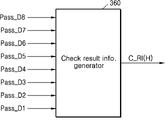
비교부(340)는 복수의 논리 회로들(LC1~LCn)을 포함할 수 있다. 논리 회로들(LC1~LCn) 각각은 XOR 논리 회로일 수 있다. 각각의 논리 회로들(LC1~LCn)은 복수의 패턴 데이터(PT_1~PT_n)와 복수의 샘플링 데이터(Sample_D1~Sample_Dn)을 각각 비교하여, 복수의 비교 결과들(Comp_R1~Comp_Rn)을 생성할 수 있다.The
체크 결과 정보 생성부(360)는 복수의 비교 결과들(Comp_R1~Comp_Rn)을 수신하고, 복수의 비교 결과들(Comp_R1~Comp_Rn)을 이용하여 체크 결과 정보를 생성할 수 있으며, 이에 대한 구체적인 내용은 도 9a 및 도 9b에서 서술한다.The check result
도 9a 및 도 9b는 도 8의 체크 결과 정보 9A and 9B are check result information of FIG. 8
생성부(360)의of the
도 9a 및 도 9b에서는 메모리 컨트롤러와 메모리 장치 사이에 8개의 병렬 데이터가 송수신되는 것을 가정한다. 도 8 및 도 9a를 참조하면, 샘플링 회로(320) 및 비교부(340)는 8개의 패턴 데이터(PT_D1~PT_D8)를 이용하여 8개의 비교 결과들(Comp_R1~Comp_R8)을 생성할 수 있으며, 생성된 비교 결과들(Comp_R1~Comp_R8)을 체크 결과 정보 생성부(360)에 제공할 수 있다. 9A and 9B , it is assumed that eight pieces of parallel data are transmitted/received between the memory controller and the memory device. 8 and 9A , the
도 9a에서의 체크 결과 정보 생성부(360)는 비교 결과들(Comp_R1~Comp_R8)로서 복수의 패스 데이터(Pass_D1~Pass_D8)를 수신할 수 있다. 일 실시예로서, 체크 결과 정보 생성부(360)는 비교 결과들(Comp_R1~Comp_R8)이 모두 패스 데이터(Pass_D1~Pass_D8)인 때에는 메모리 장치에 대한 리트레이닝 동작이 필요없음을 나타내는 제1 값(H)을 갖는 체크 결과 정보(C_RI)를 생성할 수 있다.The check result
도 9b에서의 체크 결과 정보 생성부(360)는 비교 결과들(Comp_R1~Comp_R8)로서 복수의 패스 데이터(Pass_D1, Pass_D3~Pass_D8)와 하나의 페일 데이터(Fail_D2)를 수신할 수 있다. 일 실시예로서, 체크 결과 정보 생성부(360)는 적어도 하나의 페일 데이터를 수신한 때에는 메모리 장치에 대한 리트레이닝 동작이 필요함을 나타내는 제2 값(L)을 갖는 체크 결과 정보(C_RI)를 생성할 수 있다. 다만, 이는 예시적인 실시예에 불과한 바, 이에 국한되지 않으며, 체크 결과 정보 생성부(360)는 소정의 기준 페일 데이터 개수 이상의 페일 데이터를 수신한 때에 제2 값(L)을 갖는 체크 결과 정보(C_RI)를 생성할 수 있다. 기준 페일 데이터 개수는 미리 설정될 수 있으며, 외부로부터 수신한 신호에 의하여 기준 페일 데이터 개수가 변경될 수 있다.The check result
도 10a 및 도 10b는 본 개시의 일 10A and 10B show an example of the present disclosure;
실시예에in the example
따라 패턴 데이터와 클록 Follow pattern data and clock
신호간between signals
정렬 정도를 기반으로 체크 결과 정보를 생성하는 경로 상태 체크 회로(400a, 400b)의 of the path
도 10a를 참조하면, 경로 상태 체크 회로(400a)는 샘플링 회로(420a), 비교부(440a) 및 체크 결과 정보 생성부(460a)를 포함할 수 있다. 샘플링 회로(420a)는 복수의 샘플링 회로들(420a_1~420a_m)을 포함할 수 있다. 비교부(440a)는 복수의 비교기들(440a_1~440a_m)을 포함할 수 있다. Referring to FIG. 10A , the path
샘플링 회로들(420a_1~420a_m)은 신호 전송 경로(STP)의 소정의 데이터 전송 경로를 통과한 패턴 데이터(PT_D')를 수신하고, 위상이 상이하고, 신호 전송 경로(STP)의 소정의 클록 전송 경로를 통과한 클록 신호들(CLK_P1'~CLK_Pm')을 각각 수신할 수 있다. 클록 신호들(CLK_P1~CLK_Pm)은 각각 일정한 위상 차이가 나도록 쉬프트된 것일 수 있다. 샘플링 회로들(420a_1~420a_m) 각각은 클록 신호들(CLK_P1'~CLK_Pm') 중 어느 하나와 패턴 데이터(PT_D')를 이용하여 샘플링 동작을 수행하고, 샘플링 데이터(Sample_DP1~Sample_DPm)를 생성할 수 있다. 비교기들(440a_1~440a_m) 각각은 복수의 샘플링 데이터(Sample_DP1~Sample_DPm) 중 어느 하나와 비교 기준이 되는 패턴 데이터(PT_D)를 이용하여 비교 동작을 수행하고, 비교 결과(Comp_DP1~Comp_DPm)를 생성할 수 있다. 경로 상태 정보(PSI, Path State Information)는 비교부(440a)에서 생성된 비교 결과들(Comp_DP1~Comp_DPm)을 포함할 수 있으며, 경로 상태 정보(PSI)는 현재 패턴 데이터(PT_D')와 기준 클록 신호(또는 쉬프트 위상이 0인 클록 신호, 예를 들면, CLK_P1')간의 정렬 정도를 나타낼 수 있다.The sampling circuits 420a_1 to 420a_m receive the pattern data PT_D' passing through a predetermined data transmission path of the signal transmission path STP, have different phases, and transmit a predetermined clock of the signal transmission path STP Each of the clock signals CLK_P1' to CLK_Pm' passing through the path may be received. Each of the clock signals CLK_P1 to CLK_Pm may be shifted to have a constant phase difference. Each of the sampling circuits 420a_1 to 420a_m may perform a sampling operation using any one of the clock signals CLK_P1' to CLK_Pm' and the pattern data PT_D' and generate the sampling data Sample_DP1 to Sample_DPm. there is. Each of the comparators 440a_1 to 440a_m performs a comparison operation using any one of the plurality of sampling data Sample_DP1 to Sample_DPm and the pattern data PT_D as a comparison reference, and generates comparison results Comp_DP1 to Comp_DPm. can The path state information (PSI) may include comparison results Comp_DP1 to Comp_DPm generated by the
체크 결과 정보 생성부(460a)는 경로 상태 정보(PSI) 및 기준 설정 정보(Ref_set_Info.)를 기반으로, 체크 결과 정보(C_RI)를 생성할 수 있다. 기준 설정 정보(Ref_set_Info.)는 기준 상태 정보(RSI, Reference State Information)및 기준 비트 개수(RBN, Reference Bit Number)를 포함할 수 있다. 기준 설정 정보(Ref_set_Info.)는 도 3a의 저장 회로(246a)에 저장될 수 있다. 이에 대한 구체적인 설명은 후술하도록 한다.The check result
도 10b의 경로 상태 체크 회로(400b)는 도 10a의 경로 상태 체크 회로(400a)와 비교하여, 패턴 데이터 생성부(470b) 및 클록 신호 생성부(480b)를 더 포함할 수 있다. 패턴 데이터 생성부(470n)는 신호 전송 경로(STP)의 상태를 체크하기 위하여 소정의 패턴 비트들을 포함하는 패턴 데이터(PT_D)를 생성할 수 있다. 클록 신호 생성부(480b)는 신호 전송 경로(STP)의 상태를 체크하기 위하여 소정의 주파수 및 위상을 갖는 클록 신호들(CLK_P1~CLK_Pm)을 생성할 수 있다. 클록 신호 생성부(480b)는 위상 쉬프터(482b)를 포함할 수 있으며, 위상 쉬프터(482b)를 이용하여 위상이 0인 기준 클록 신호를 일정한 위상만큼 계속 쉬프트시켜, 위상이 상이한 복수의 클록 신호들(CLK_P1~CLK_Pm)을 생성할 수 있다. Compared to the path
도 11은 도 10a의 기준 상태 정보(Ref_state_Info.)에 대한 설명을 하기 위한 도면이다.11 is a diagram for explaining the reference state information (Ref_state_Info.) of FIG. 10A.
도 10a 및 도 11을 참조하면, 메모리 장치에 대한 트레이닝 동작 후, 소정의 시간내에 경로 상태 체크 회로(400a)는 기준 상태 정보(RSI)를 생성할 수 있다. 샘플링 회로(420a)는 제1 클록 신호(CLK_P1', Ref.) 및 제1 클록 신호(CLK_P1', Ref.)를 기준으로 소정의 위상(Φ)만큼 각각 쉬프트된 제2 내지 제4 클록 신호(CLK_P2'~CLK_P4')를 이용하여 제1 비트 데이터(D_1) 및 제2 비트 데이터(D_2)를 포함하는 패턴 데이터(PT_D')에 대한 복수의 샘플링 동작을 수행할 수 있다. 10A and 11 , after a training operation for the memory device, the path
비교부(440a)는 샘플링 회로(420a)로부터 생성된 복수의 샘플링 데이터와 패턴 데이터(PT_D)를 비교하여, 복수의 비교 결과들(Comp_DP1~Comp_DP4)을 생성할 수 있다. 예를 들어, 기준이 되는 제1 클록 신호(CLK_P1')를 이용하여 생성된 샘플링 데이터는 패턴 데이터(PT_D)와 일치하기 때문에, 비교부(440a)는 패스(Pass) 결과를 나타내는 값(예를 들면, '1'의 값)을 갖는 제1 비교 결과(Comp_DP1)를 생성할 수 있다. 이와 같은 방식으로, 제1 클록 신호(CLK_P1')를 기준으로 각각 Φ, 2Φ 만큼 쉬프트된 제2 및 제3 클록 신호(CLK_P2', CLK_P3')를 이용하여 생성된 샘플링 데이터는 패턴 데이터(PT_D)와 각각 일치하기 때문에, 비교부(440b)는 패스(Pass) 결과를 나타내는 값을 갖는 제2 및 제3 비교 결과(Comp_DP2, Comp_DP3)를 생성할 수 있다. 또한, 제1 클록 신호(CLK_P1')를 기준으로 3Φ 만큼 쉬프트된 제4 클록 신호(CLK_P4')를 이용하여 생성된 샘플링 데이터는 패턴 데이터(PT_D)와 불일치하기 때문에, 비교부(440b)는 페일(Fail) 결과를 나타내는 값(예를 들면, '0'의 값)을 갖는 제4 비교 결과(Comp_DP4)를 생성할 수 있다.The
기준 상태 정보(RSI)는 제1 내지 제4 비교 결과(Comp_DP1~Comp_DP4)를 포함할 수 있으며, 일 예로, 4비트 데이터로서 '0111' 값을 가질 수 있다. 기준 상태 정보(RSI)는 메모리 장치에 대한 트레이닝 동작 후, 소정의 시간내에 생성된 것으로서, 메모리 장치에 대한 리트레이닝 동작이 필요한지 여부를 결정하기 위한 기준이 될 수 있다.The reference state information RSI may include the first to fourth comparison results Comp_DP1 to Comp_DP4, and for example, may have a value of '0111' as 4-bit data. The reference state information RSI is generated within a predetermined time after a training operation for the memory device, and may be a criterion for determining whether a retraining operation for the memory device is required.
도 12a Figure 12a 내지 도to degree 13b는 본 개시의 일 13b is one of the present disclosure 실시예에in the example 따른 경로 상태 정보(PSI)를 이용하여 체크 결과 정보(C_RI)를 생성하는 경로 상태 체크 회로의 동작을 설명하기 위한 도면이다. It is a diagram for explaining the operation of the path state check circuit that generates the check result information C_RI by using the path state information PSI.
도 10a 및 도 12a를 참조하면, 외부로부터 신호 전송 경로 상태 체크 관련 커맨드를 수신하거나 특정 값을 갖는 어드레스 신호를 수신한 경우, 또는 메모리 장치의 트레이닝 동작 후 소정의 주기마다 경로 상태 체크 회로(400a)는 경로 상태 정보(PSI)를 생성하는 동작을 수행할 수 있다. 이하에서는, 도 11과 달리, 메모리 장치에 대한 트레이닝 동작 후에 소정이 시간이 지난 결과, 신호 전송 경로를 통과한 데이터 및 클록 신호간의 정렬이 어느 정도 틀어진 것을 가정한다.10A and 12A , when a signal transmission path status check related command is received from the outside or an address signal having a specific value is received, or after a training operation of the memory device, the path
샘플링 회로(420a)는 제1 클록 신호(CLK_P1', Ref.) 및 제1 클록 신호(CLK_P1', Ref.)를 기준으로 소정의 위상(Φ)만큼 각각 쉬프트된 제2 내지 제4 클록 신호(CLK_P2'~CLK_P4')를 이용하여 제1 비트 데이터(D_1) 및 제2 비트 데이터(D_2)를 포함하는 패턴 데이터(PT_D')에 대한 복수의 샘플링 동작을 수행할 수 있다. 비교부(440a)는 샘플링 회로(420a)로부터 생성된 복수의 샘플링 데이터와 패턴 데이터(PT_D)를 비교하여, 복수의 비교 결과들(Comp_DP1~Comp_DP4)을 생성할 수 있다. 기준이 되는 제1 클록 신호(CLK_P1') 및 제2 클록 신호(CLK_P2')를 이용하여 각각 생성된 샘플링 데이터는 패턴 데이터(PT_D)와 일치하기 때문에, 비교부(440a)는 패스(Pass) 결과를 나타내는 값을 갖는 제1 및 제2 비교 결과(Comp_DP1, Comp_DP2)를 생성할 수 있다. 또한, 제3 및 제4 클록 신호(CLK_P3', CLK_P4')를 이용하여 각각 생성된 샘플링 데이터는 패턴 데이터(PT_D)와 불일치하여, 비교부(440a)는 페일(Fail) 결과를 나타내는 값을 갖는 제3 및 제4 비교 결과(Comp_DP3, Comp_DP4)를 생성할 수 있다.The
경로 상태 정보(PSI)는 제1 내지 제4 비교 결과(Comp_DP1~Comp_DP4)를 포함할 수 있으며, 일 예로, 4비트 데이터로서 '0011' 값을 가질 수 있다.The path state information PSI may include the first to fourth comparison results Comp_DP1 to Comp_DP4, and for example, may have a value of '0011' as 4-bit data.
도 12b를 참조하면, 체크 결과 정보 생성부(460)는 경로 상태 정보(PSI) 및 기준 설정 정보(Ref_set_Info.)를 기반으로 메모리 장치에 대한 리트레이닝 동작이 필요한지 여부를 나타내는 체크 결과 정보(C_RI)를 생성할 수 있다. 기준 설정 정보(Ref_set_Info.)는 기준 상태 정보(RSI) 및 기준 비트 개수(RBN)를 포함할 수 있다. 기준 상태 정보(RSI)는 도 11에서 전술한 바와 같이, '0111' 값으로 설정될 수 있으며, 기준 비트 개수(RBN)는 '2'로 설정될 수 있다. 일 실시예로, 기준 비트 개수(RBN)는 기준 상태 정보(RSI)를 기반으로 설정될 수 있다. 구체적으로, 기준 상태 정보(RSI)가 포함하는 비트의 개수, 기준 상태 정보(RSI)의 값을 고려하여 기준 비트 개수(RBN)가 설정될 수 있다. 다만, 기준 상태 정보(RSI)의 값과 기준 비트 개수(RBN)의 값은 예시적인 것으로, 이에 국한되지 않으며, 다양한 값으로 설정될 수 있으며, 메모리 장치의 동작 환경 등에 따른 요인으로 값이 변경될 수 있다. Referring to FIG. 12B , the check result
체크 결과 정보 생성부(460)는 경로 상태 정보(PSI)와 기준 상태 정보(RSI)를 비교할 수 있다. 체크 결과 정보 생성부(460)는 경로 상태 정보(PSI)와 기준 상태 정보(RSI)간의 상이한 비트 개수가 기준 비트 개수(RBN) 이상인지 여부를 기반으로 체크 결과 정보(C_RI)를 생성할 수 있다. 일 예로, 경로 상태 정보(PSI)의 값은 '0011'이고, 기준 상태 정보(RSI)의 값은 '0111'이므로, 한 개의 비트가 상이하며, 이는 '2'로 설정된 기준 비트 개수(RBN)보다 작다. The check result
경로 상태 정보(PSI)와 기준 상태 정보(RSI)간의 차이가 크지 않은 것을 볼 때, 데이터와 클록 신호간의 정렬이 틀어진 정도가 메모리 동작이 페일될 정도에 이르지 않았다고 판단될 수 있는 바, 이에 따라, 체크 결과 정보 생성부(460)는 메모리 장치에 대한 리트레이닝 동작이 필요 없음을 나타내는 제1 값(H)을 갖는 체크 결과 정보(C_RI)를 생성할 수 있다. Considering that the difference between the path state information (PSI) and the reference state information (RSI) is not large, it can be determined that the degree of misalignment between the data and the clock signal does not reach the extent to which the memory operation fails. The check result
도 10a 및 도 13a를 참조하면, 샘플링 회로(420a)는 제1 클록 신호(CLK_P1', Ref.) 및 제1 클록 신호(CLK_P1', Ref.)를 기준으로 소정의 위상(Φ) 간격만큼 각각 쉬프트된 제2 내지 제4 클록 신호(CLK_P2'~CLK_P4')를 이용하여 제1 비트 데이터(D_1) 및 제2 비트 데이터(D_2)를 포함하는 패턴 데이터(PT_D')에 대한 복수의 샘플링 동작을 수행할 수 있다. 비교부(440a)는 샘플링 회로(420a)로부터 생성된 복수의 샘플링 데이터와 패턴 데이터(PT_D)를 비교하여, 복수의 비교 결과들(Comp_DP1~Comp_DP4)을 생성할 수 있다. 기준이 되는 제1 클록 신호(CLK_P1') 를 이용하여 각각 생성된 샘플링 데이터는 패턴 데이터(PT_D)와 일치하기 때문에, 비교부(440a)는 패스(Pass) 결과를 나타내는 값을 갖는 제1 비교 결과(Comp_DP1)를 생성할 수 있다. 또한, 제2 내지 제4 클록 신호(CLK_P2'~CLK_P4')를 이용하여 각각 생성된 샘플링 데이터는 패턴 데이터(PT_D)와 불일치하기 때문에, 비교부(440a)는 페일(Fail) 결과를 나타내는 값을 갖는 제2 내지 제4 비교 결과(Comp_DP2~Comp_DP4)를 생성할 수 있다.Referring to FIGS. 10A and 13A , the
경로 상태 정보(PSI)는 제1 내지 제4 비교 결과(Comp_DP1~Comp_DP4)를 포함할 수 있으며, 일 예로, 4비트 데이터로서 '0001' 값을 가질 수 있다.The path state information PSI may include the first to fourth comparison results Comp_DP1 to Comp_DP4, and for example, may have a value of '0001' as 4-bit data.
도 13b를 참조하면, 체크 결과 정보 생성부(460)는 경로 상태 정보(PSI)와 기준 상태 정보(RSI)를 비교할 수 있다. 체크 결과 정보 생성부(460)는 경로 상태 정보(PSI)와 기준 상태 정보(RSI)간의 상이한 비트 개수가 기준 비트 개수(RBN) 이상인지 여부를 기반으로 체크 결과 정보(C_RI)를 생성할 수 있다. 일 예로, 경로 상태 정보(PSI)의 값은 '0001'이고, 기준 상태 정보(RSI)의 값은 '0111'이므로, 한 개의 비트가 상이하며, 이는 '2'로 설정된 기준 비트 개수(RBN)와 동일하다.Referring to FIG. 13B , the check
경로 상태 정보(PSI)와 기준 상태 정보(RSI)간의 차이(기준 비트 개수(RBN) 이상)가 크기 때문에 데이터와 클록 신호간의 정렬이 틀어진 정도가 메모리 동작이 페일될 정도에 이르렀다고 판단될 수 있는 바, 이에 따라, 체크 결과 정보 생성부(460)는 메모리 장치에 대한 리트레이닝 동작이 필요함을 나타내는 제2 값(L)을 갖는 체크 결과 정보(C_RI)를 생성할 수 있다.Because the difference between the path state information (PSI) and the reference state information (RSI) (more than the number of reference bits (RBN)) is large, it can be determined that the degree of misalignment between the data and the clock signal has reached a level that the memory operation fails. Accordingly, the check result
도 14a Figure 14a 내지 도to degree 14d는 본 개시에 따른 경로 상태 체크 회로가 신호 전송 14d shows that the path state check circuit according to the present disclosure transmits a signal 경로에 대한 체크 동작check action on path 및 메모리 장치의 라이트 동작을 수행하는 타이밍을 설명하기 위한 and a timing for performing a write operation of the memory device. 타이밍도이다it's a timing chart ..
도 1 및 도 14a를 참조하면, 메모리 장치(20)가 메모리 컨트롤러(10)로부터 어떠한 커맨드를 수신하지 않은 상태 또는 유휴(idle) 시간에 경로 상태 체크 회로(24)는 신호 전송 경로에 대한 체크 동작(CHO, Check Operation)을 수행할 수 있다. 경로 상태 체크 회로(24)는 신호 전송 경로의 상태가 양호한 때에는 경로 상태 체크 회로(24)에 의해 생성된 체크 결과 정보(C_RI)는 메모리 장치(20)에 대한 리트레이닝 동작이 필요 없음을 나타내는 제1 값(H)을 가질 수 있다. 메모리 장치(20)가 메모리 컨트롤러(10)로부터 수신한 라이트 커맨드(WR_CMD)에 응답하여 메모리 장치(20)는 바로 라이트 동작(WRO, Write operation)을 수행할 수 있다.1 and 14A , in a state in which the
도 1 및 도 14b를 참조하면, 메모리 장치(20)가 라이트 커맨드(WR_CMD)에 응답하여 라이트 동작(WRO)을 수행하기 전 타이밍에 경로 상태 체크 회로(24)는 신호 전송 경로에 대한 체크 동작(CHO)을 수행할 수 있다. 즉, 메모리 장치(20)가 메모리 컨트롤러(10)로부터 라이트 커맨드(WR_CMD)를 수신한 때에, 경로 상태 체크 회로(24)는 신호 전송 경로에 대한 체크 동작을 먼저 수행할 수 있다. 경로 상태 체크 회로(24)에 의해 생성된 체크 결과 정보(C_RI)가 메모리 장치(20)에 대한 리트레이닝 동작이 필요 없음을 나타내는 제1 값(H)을 갖는 때에, 체크 동작(CHO) 이후에 메모리 장치(20)는 라이트 커맨드(WR_CMD)에 응답하여 바로 라이트 동작(WRO)을 수행할 수 있다.1 and 14B , at a timing before the
도 1 및 도 14c를 참조하면, 경로 상태 체크 회로(24)는 메모리 장치(20)가 소정의 라이트 동작을 수행하는 도중 타이밍에 신호 전송 경로에 대한 체크 동작을 수행할 수 있다. 즉, 메모리 장치(20)는 메모리 컨트롤러(10)로부터 수신한 라이트 커맨드(WR_CMD)에 응답하여 일부 라이트 동작(WRO_P1)을 수행하고 난 후에, 경로 상태 체크 회로(24)는 신호 전송 경로에 대한 체크 동작(CHO)을 수행할 수 있다. 메모리 장치(20)는 나머지 라이트 동작(WRO_P2)을 체크 동작(CHO)이 완료 후에 수행할 수 있다. 경로 상태 체크 회로(24)에 의해 생성된 체크 결과 정보(C_RI)가 메모리 장치(20)에 대한 리트레이닝 동작이 필요 없음을 나타내는 제1 값(H)을 갖는 때에, 체크 동작(CHO) 이후에 메모리 장치(20)는 바로 나머지 라이트 동작(WRO_P2)을 수행할 수 있다.1 and 14C , the path
도 1 및 도 14d를 참조하면, 경로 상태 체크 회로(24)는 메모리 장치(20)가 라이트 동작을 완료한 이후 타이밍에 신호 전송 경로에 대한 체크 동작을 수행할 수 있다. 즉, 메모리 장치(20)는 메모리 컨트롤러(10)로부터 메모리 컨트롤러(10)로부터 수신한 라이트 커맨드(WR_CMD)에 응답하여 라이트 동작(WRO)을 수행할 수 있다. 이후, 경로 상태 체크 회로(24)는 신호 전송 경로에 대한 체크 동작(CHO)을 수행할 수 있다.1 and 14D , the path
도 14a 내지 도 14d에서는 서술의 편의상 경로 상태 체크 회로(24)는 별도의 커맨드를 수신하지 않아도 신호 전송 경로에 대한 체크 동작을 수행하는 것으로 도시되어 있으나, 전술한 바와 같이, 메모리 컨트롤러(10)로부터 신호 전송 경로 상태 체크 관련 커맨드를 수신하거나 특정 값을 갖는 어드레스 신호를 수신한 경우, 또는 메모리 장치(20)의 트레이닝 동작 후 소정의 주기마다 경로 상태 체크 회로(24)는 신호 전송 경로에 대한 체크 동작을 수행할 수 있다. 14A to 14D , for convenience of description, the path
또한, 일 실시예로, 경로 상태 체크 회로(24)는 메모리 장치(20)가 레이턴시 모드(Latency mode)일 때에, 레이턴시 모드에서 소정의 시간이 지난 후에 형성된 클록 신호를 이용하여 신호 전송 경로에 대한 체크 동작을 수행할 수 있다. 레이턴시 모드는 메모리 장치(20)가 메모리 동작을 수행하기 전에 메모리 동작에 필요한 클록 신호를 형성하는 메모리 장치(20)의 모드를 지칭할 수 있다. 즉, 경로 상태 체크 회로(24)는 메모리 동작을 수행하기 직전에 형성된 소정의 주기만큼의 클록 신호를 이용하여 체크 동작을 수행할 수 있다.Also, according to an embodiment, when the
도 15a Figure 15a 내지 도to degree 15c는 라이트 데이터( 15c is the light data ( WRWR _DATA)와 패턴 데이터(PT_D)의 배치 관계에 따른 경로 상태 체크 회로의 체크 동작 및 메모리 장치(MD)의 라이트 동작을 설명하기 위한 도면이다. _DATA) and pattern data PT_D are diagrams for explaining a check operation of the path state check circuit and a write operation of the memory device MD according to the arrangement relationship of the pattern data PT_D.
도 15a를 참조하면, 메모리 장치(MD)는 메모리 컨트롤러로부터 라이트 커맨드(WR_CMD) 및 어드레스 신호(ADDR)를 수신할 수 있다. 이후, 메모리 장치(MD)는 패턴 데이터(PT_D) 및 라이트 데이터(WR_DATA)를 포함하는 데이터를 수신할 수 있다. 일 실시예로, 패턴 데이터(PT_D)는 라이트 데이터(WR_DATA)의 앞단에 배치될 수 있다. 메모리 장치(MD)의 경로 상태 체크 회로는 패턴 데이터(PT_D)를 수신한 t1 시간부터 신호 전송 경로 상태를 체크하는 동작(CHO)을 수행할 수 있다. 이하에서는, 체크 동작(CHO) 결과, 메모리 장치(MD)에 대한 리트레이닝 동작이 필요 없음을 나타내는 제1 값(H)을 갖는 체크 결과 정보(C_RI)가 생성됨을 가정한다. 메모리 장치(MD)는 t2 시간부터 t3 시간까지 도 2의 페이지 버퍼 회로(120)에 라이트 데이터(WR_DATA)를 라이트하는 동작(WRO_PB)을 수행할 수 있다. 이후, 메모리 컨트롤러로부터 확인 커맨드(CON_CMD)를 수신한 때에, 메모리 장치(MD)는 t4 시간부터 페이즈 버퍼 회로(120)에 저장된 라이트 데이터(WR_DATA)를 도 2의 메모리 셀 어레이(160)에 라이트하는 동작(WRO_MCELL)을 수행할 수 있다. 즉, 컨펌 커맨드(CON_CMD)는 페이지 버퍼 회로(120)에 라이트된 데이터를 최종적으로 메모리 셀 어레이(160)에 라이트할 것을 메모리 장치(MD)에 지시하는 커맨드일 수 있다.Referring to FIG. 15A , the memory device MD may receive a write command WR_CMD and an address signal ADDR from the memory controller. Thereafter, the memory device MD may receive data including the pattern data PT_D and the write data WR_DATA. In an embodiment, the pattern data PT_D may be disposed in front of the write data WR_DATA. The path state check circuit of the memory device MD may perform an operation CHO of checking the signal transmission path state from a time t1 when the pattern data PT_D is received. Hereinafter, it is assumed that, as a result of the check operation CHO, check result information C_RI having a first value H indicating that a retraining operation for the memory device MD is not required is generated. The memory device MD may perform an operation WRO_PB of writing the write data WR_DATA to the
도 15b를 참조하면, 도 15b와 달리, 패턴 데이터(PT_D)는 제1 라이트 데이터(WR_DATA_1) 및 제2 라이트 데이터(WR_DATA_2) 사이에 배치될 수 있다. 메모리 장치(MD)는 t1 시간부터 도 2의 페이지 버퍼 회로(120)에 제1 라이트 데이터(WR_DATA_1)를 라이트하는 동작(WRO_PB_1)을 수행할 수 있다. 메모리 장치(MD)의 경로 상태 체크 회로는 패턴 데이터(PT_D)를 수신한 t2 시간부터 신호 전송 경로 상태를 체크하는 동작(CHO)을 수행할 수 있다. 메모리 장치(MD)는 t3 시간부터 도 2의 페이지 버퍼 회로(120)에 제2 라이트 데이터(WR_DATA_2)를 라이트하는 동작(WRO_PB_2)을 수행할 수 있다. 이후, 메모리 컨트롤러로부터 확인 커맨드(CON_CMD)를 수신한 때에, 메모리 장치(MD)는 t5 시간부터 페이즈 버퍼 회로(120)에 저장된 제1 및 제2 라이트 데이터(WR_DATA_1, WR_DATA_2)를 도 2의 메모리 셀 어레이(160)에 라이트하는 동작(WRO_MCELL)을 수행할 수 있다.Referring to FIG. 15B , unlike FIG. 15B , the pattern data PT_D may be disposed between the first write data WR_DATA_1 and the second write data WR_DATA_2 . The memory device MD may perform an operation WRO_PB_1 of writing the first write data WR_DATA_1 to the
도 15c는 도 15a와 달리, 패턴 데이터(PT_D)는 라이트 데이터(WR_DATA)의 뒷단에 배치될 수 있다. 메모리 장치(MD)는 t1 시간부터 도 2의 페이지 버퍼 회로(120)에 라이트 데이터(WR_DATA)를 라이트하는 동작(WRO_PB)을 수행할 수 있다. 메모리 장치(MD)의 경로 상태 체크 회로는 패턴 데이터(PT_D)를 수신한 t2 시간부터 t3 시간까지 신호 전송 경로 상태를 체크하는 동작(CHO)을 수행할 수 있다. 이후, 메모리 컨트롤러로부터 확인 커맨드(CON_CMD)를 수신한 때에, 메모리 장치(MD)는 t4 시간부터 페이지 버퍼 회로(120)에 저장된 라이트 데이터(WR_DATA)를 도 2의 메모리 셀 어레이(160)에 라이트하는 동작(WRO_MCELL)을 수행할 수 있다.In FIG. 15C , unlike FIG. 15A , the pattern data PT_D may be disposed at a rear end of the write data WR_DATA. The memory device MD may perform an operation WRO_PB of writing the write data WR_DATA to the
도 16a Figure 16a 내지 도to degree 16c는 본 개시에 따른 경로 상태 체크 회로로부터 생성된 체크 결과 정보를 기반으로 한 메모리 장치의 동작을 설명하기 위한 16c is for explaining the operation of the memory device based on the check result information generated by the path status check circuit according to the present disclosure. 타이밍도이다it's a timing chart ..
도 1 및 도 16a를 참조하면, 메모리 장치(20)가 메모리 컨트롤러(10)로부터 라이트 커맨드(WR_CMD)를 수신한 때에, 경로 상태 체크 회로(24)는 신호 전송 경로의 체크 동작을 수행할 수 있다. 이후, 메모리 장치(20)는 라이트 동작(WRO)을 수행할 때에, 체크 결과 정보(C_RI)를 참조하여, 라이트 동작(WRO) 수행 여부를 결정할 수 있다. 경로 상태 체크 회로(24)에 의해 생성된 체크 결과 정보(C_RI)가 메모리 장치(20)에 대한 리트레이닝 동작이 필요함을 나타내는 제2 값(L)을 갖는 때에, 메모리 장치(20)는 라이트 동작을 중지(WROS, Write Operation Stop)할 수 있다. 메모리 장치(20)가 라이트 동작을 중지(WROS)하는 것은 메모리 장치(20)가 라이트 커맨드(WR_CMD)에 응답하여 일련의 라이트 동작 수행을 하지 않는 상태인 것으로 정의할 수 있다. 다만, 이는 예시적 실시예에 불과한 바, 이에 국한되지 않으며, 라이트 동작을 중지(WROS)하는 것은 다양한 정의가 가능하며, 다른 정의의 예는 도 17a 및 도 17b에서 서술한다. 1 and 16A , when the
메모리 컨트롤러(10)는 체크 결과 정보(C_RI)를 참조하여, 리트레이닝 커맨드(RT_CMD)를 메모리 장치(20)에 제공할 수 있다. 메모리 장치(20)는 리트레이닝 커맨드(RT_CMD)에 응답하여, 메모리 장치(20)는 리트레이닝 동작(RE_TRO)을 수행할 수 있다. 리트레이닝 수행(RE_TRO) 결과, 체크 결과 정보(C_RI)는 메모리 장치(20)에 대한 리트레이닝 동작이 필요 없음을 나타내는 제1 값(H)으로 변경될 수 있으며, 메모리 장치(20)는 라이트 동작(WRO)을 수행할 수 있다.The
도 1 및 도 16b를 참조하면, 메모리 장치(20)가 메모리 컨트롤러(10)로부터 라이트 커맨드(WR_CMD)를 수신한 때에, 메모리 장치(20)는 라이트 커맨드(WR_CMD)에 응답하여 일부 라이트 동작(WRO_P1)을 수행하고 난 후에, 경로 상태 체크 회로(24)는 신호 전송 경로의 체크 동작(CHO)을 수행할 수 있다. 경로 상태 체크 회로(24)에 의해 생성된 체크 결과 정보(C_RI)가 메모리 장치(20)에 대한 리트레이닝 동작이 필요함을 나타내는 제2 값(L)을 갖는 때에, 메모리 장치(20)는 라이트 동작을 중지(WROS)할 수 있다. 1 and 16B , when the
메모리 컨트롤러(10)는 체크 결과 정보(C_RI)를 참조하여, 리트레이닝 커맨드(RT_CMD)를 메모리 장치(20)에 제공할 수 있다. 메모리 장치(20)는 리트레이닝 커맨드(RT_CMD)에 응답하여, 메모리 장치(20)는 리트레이닝 동작(RE_TRO)을 수행할 수 있다. 리트레이닝 수행(RE_TRO) 결과, 체크 결과 정보(C_RI)는 메모리 장치(20)에 대한 리트레이닝 동작이 필요 없음을 나타내는 제1 값(H)으로 변경될 수 있으며, 메모리 장치(20)는 나머지 라이트 동작(WRO_P2)을 수행할 수 있다. 더 나아가, 메모리 장치(20)는 데이터와 클록 신호간의 정렬이 틀어진 상태에서 수행된 일부 라이트 동작(WRO_P1)에서 메모리 셀 어레이(22)에 라이트된 데이터에 대하여 리라이트 동작(RE_WRO_P1)을 선택적으로 수행할 수 있다.The
도 1 및 도 16c를 참조하면, 메모리 장치(20)는 메모리 컨트롤러(10)로부터 수신한 라이트 커맨드(WR_CMD)에 응답하여 라이트 동작(WRO)을 수행할 수 있다. 이후, 경로 상태 체크 회로(24)는 신호 전송 경로의 체크 동작(CHO)을 수행할 수 있다. 경로 상태 체크 회로(24)에 의해 생성된 체크 결과 정보(C_RI)가 메모리 장치(20)에 대한 리트레이닝 동작이 필요함을 나타내는 제2 값(L)을 가질 수 있다. 1 and 16C , the
메모리 컨트롤러(10)는 체크 결과 정보(C_RI)를 참조하여, 리트레이닝 커맨드(RT_CMD)를 메모리 장치(20)에 제공할 수 있다. 메모리 장치(20)는 리트레이닝 커맨드(RT_CMD)에 응답하여, 메모리 장치(20)는 리트레이닝 동작(RE_TRO)을 수행할 수 있다. 리트레이닝 수행(RE_TRO) 결과, 체크 결과 정보(C_RI)는 메모리 장치(20)에 대한 리트레이닝 동작이 필요 없음을 나타내는 제1 값(H)으로 변경될 수 있으며, 메모리 장치(20)는 데이터와 클록 신호간의 정렬이 틀어진 상태에서 수행된 라이트 동작(WRO)을 다시 수행하는 리라이트 동작(RE_WRO)을 선택적으로 수행할 수 있다.The
이와 같이, 메모리 장치(20)는 경로 상태 체크 회로(24)로부터 생성된 체크 결과 정보(C_RI)를 참조한 결과, 메모리 장치(20)에 대한 리트레이닝 동작이 필요한 경우에는 라이트 동작의 결과가 페일될 가능성이 높기 때문에, 리트레이닝 동작을 수행하기 전에는 라이트 동작을 수행하지 않음으로써, 불필요한 메모리 동작을 수행하지 않는 효과가 있다.As such, when the
도 17a 및 도 17b는 도 16a 17a and 17b are shown in Fig. 16a 내지 도to degree 16c의 메모리 장치(MD)의 라이트 동작 중지(WROS)에 대한 다른 예를 설명하기 위한 도면이다. 16c is a diagram for explaining another example of the write operation stop (WROS) of the memory device MD.
도 17a 및 도 17b의 구체적인 내용은 도 15a에서 서술된 바, 이하 특징적인 내용을 중심으로 서술하도록 한다. 이하에서는, 체크 동작(CHO) 결과, 메모리 장치(MD)에 대한 리트레이닝 동작이 필요함을 나타내는 제2 값(L)을 갖는 체크 결과 정보(C_RI)가 생성됨을 가정한다.The specific contents of FIGS. 17A and 17B are described with reference to FIG. 15A, and below, characteristic contents will be mainly described. Hereinafter, it is assumed that, as a result of the check operation CHO, check result information C_RI having a second value L indicating that a retraining operation for the memory device MD is required is generated.
도 17a를 참조하면, 메모리 장치(MD)의 경로 상태 체크 회로로부터 생성된 체크 결과 정보(CHO)는 메모리 컨트롤러(MCTR)에 제공될 수 있다. 메모리 컨트롤러(MCTR)가 체크 결과 정보(CHO)를 제공받는 구체적인 실시예는 도 18a 및 도 18b에서 서술하도록 한다. 메모리 컨트롤러(MCTR)는 체크 결과 정보(C_RI)를 참조하여, 메모리 장치(MD)에 대한 리트레이닝 동작이 필요함을 인지할 수 있다. 또한, 메모리 장치(MD)의 도 2의 페이지 버퍼 회로(120)에 라이트 데이터(WR_DATA)를 라이트하는 동작(WRO_PB)은 신뢰성이 낮은 바, 메모리 컨트롤러(MCTR)는 확인 커맨드(CON_CMD)를 메모리 장치(MD)에 제공하지 않을 수 있다. 이후, 메모리 장치(MD)는 페이지 버퍼 회로(120)에 저장된 라이트 데이터(WR_DATA)를 도 2의 메모리 셀 어레이(160)에 라이트하는 동작을 수행하지 않을 수 있다. 즉, 메모리 장치(MD)는 라이트 동작을 중지(WROS)하는 것은 페이지 버퍼 회로(120)에 저장된 라이트 데이터(WR_DATA)를 메모리 셀 어레이(160)에 라이트하는 동작을 수행하지 않는 상태인 것으로 정의할 수 있다.Referring to FIG. 17A , the check result information CHO generated by the path state check circuit of the memory device MD may be provided to the memory controller MCTR. A specific embodiment in which the memory controller MCTR receives the check result information CHO will be described with reference to FIGS. 18A and 18B . The memory controller MCTR may recognize that a retraining operation is required for the memory device MD by referring to the check result information C_RI. In addition, since the operation WRO_PB of writing the write data WR_DATA to the
도 17b를 참조하면, 도 17a와 달리, 메모리 장치(MD)의 경로 상태 체크 회로로부터 생성된 체크 결과 정보(CHO)는 메모리 컨트롤러(MCTR)에 바로 제공되지 않을 수 있다. 이러한 경우, 메모리 컨트롤러(MCTR)는 메모리 장치(MD)에 대한 리트레이닝 동작이 필요한지 여부를 알 수 없어, 메모리 장치(MD)에 확인 커맨드(CON_CMD)를 제공할 수 있다. 메모리 장치(MD)는 확인 커맨드(CON_CMD)를 수신한 때에, 체크 결과 정보(C_RI)를 참조하여, 페이지 버퍼 회로(120)에 저장된 라이트 데이터(WR_DATA)를 도 2의 메모리 셀 어레이(160)에 라이트하는 동작을 수행할지 여부를 결정할 수 있다. 예를 들어, 체크 결과 정보(C_RI)가 메모리 장치(MD)에 대한 리트레이닝 동작이 필요함을 나타내는 제2 값(L)을 갖는 때에는, 메모리 장치(MD)는 확인 커맨드(CON_CMD)를 수신하였더라도 페이지 버퍼 회로(120)에 저장된 라이트 데이터(WR_DATA)를 도 2의 메모리 셀 어레이(160)에 라이트하는 동작을 수행하지 않을 수 있다. 즉, 메모리 장치(MD)는 라이트 동작을 중지(WROS)할 수 있다.Referring to FIG. 17B , unlike FIG. 17A , the check result information CHO generated by the path state check circuit of the memory device MD may not be directly provided to the memory controller MCTR. In this case, the memory controller MCTR may not know whether a retraining operation is required for the memory device MD, and thus may provide the check command CON_CMD to the memory device MD. When the check command CON_CMD is received, the memory device MD transfers the write data WR_DATA stored in the
도 18a 및 도 18b는 메모리 컨트롤러(510a, 510b)가 메모리 장치(530a, 530b)로부터 체크 결과 정보(C_RI)를 수신하는 18A and 18B illustrate a method in which the
도 18a를 참조하면, 메모리 시스템(500a)은 메모리 컨트롤러(510a) 및 메모리 장치(530a)를 포함할 수 있다. 메모리 장치(530a)는 도 1 등에서 상술한 경로 상태 체크 회로(532a)를 포함할 수 있다. 메모리 컨트롤러(510a)는 신호 전송 경로의 상태의 체크 동작을 제어하기 위한 체크 커맨드(Check_CMD)를 메모리 장치(530a)에 제공할 수 있다. 경로 상태 체크 회로(532a)는 체크 커맨드(Check_CMD)에 응답하여 신호 전송 경로에 대한 체크 동작을 수행하고, 메모리 장치(530a)의 리트레이닝 동작이 필요한지 여부를 나타내는 체크 결과 정보(C_RI)를 생성할 수 있다. 메모리 장치(530a)는 신호 전송 경로에 대한 체크 동작이 완료된 후에, 생성된 체크 결과 정보(C_RI)를 메모리 컨트롤러(510a)에 제공할 수 있다. 메모리 컨트롤러(510a)는 체크 결과 정보(C_RI)를 참조하여, 메모리 장치(530a)에 대한 리트레이닝 동작 수행 여부를 신속하게 결정할 수 있으며, 리트레이닝 동작 수행이 결정된 때에는, 리트레이닝 커맨드(RT_CMD)를 메모리 장치(530a)에 제공할 수 있다.Referring to FIG. 18A , the
도 18b를 참조하면, 도 18a와 달리, 메모리 컨트롤러(510b)는 경로 상태 체크 회로(532b)로부터 생성된 체크 결과 정보(C_RI)를 획득하기 위하여, 요청 신호를 메모리 장치(530b)에 제공할 수 있다. 일 실시예로, 체크 결과 정보(C_RI)는 메모리 장치(530b)의 상태를 나타내는 정보가 저장된 상태 레지스터에 저장될 수 있다. 이에 따라, 메모리 컨트롤러(510b)는 상태 리드 신호(Status read)를 메모리 장치(530b)에 제공할 수 있다. 메모리 장치(530b)는 상태 리드 신호(Status read) 에 응답하여 체크 결과 정보(C_RI)를 포함하는 상태 정보(Status_Info.)를 메모리 컨트롤러(510b)에 제공할 수 있다. 메모리 컨트롤러(510b)는 체크 결과 정보(C_RI)를 참조하여, 메모리 장치(530b)에 대한 리트레이닝 동작 수행 여부를 신속하게 결정할 수 있으며, 리트레이닝 동작 수행이 결정된 때에는, 리트레이닝 커맨드(RT_CMD)를 메모리 장치(530b)에 제공할 수 있다.Referring to FIG. 18B , unlike FIG. 18A , the
도 19는 본 개시의 일 19 is an example of the present disclosure;
실시예에in the example
따른 저장 장치(1000)를 나타내는 representing the
도 19를 참조하면, 저장 장치(1000)는 마스터(또는, 컨트롤러, 1100) 및 복수의 슬레이브들(또는, 메모리 칩들, 1200)을 포함할 수 있다. 슬레이브들(Slave) 각각은 데이터를 저장할 수 있는 복수의 메모리 셀들을 포함할 수 있다. 마스터(1100)는 슬레이브들(1200)에 대한 데이터 처리 동작, 예컨대 라이트 동작, 리드 동작, 이레이즈 동작, 트레이닝 동작, 리트레이닝 동작 등을 제어할 수 있다. 마스터(1100)와 슬레이브들(1200)은 복수의 채널들(CH1~CHk)을 통해 연결되어 있으며, 복수의 채널들(CH0~CHk)을 통해 마스터(1100)와 슬레이브들(1200)간에 다양한 데이터, 커맨드, 어드레스 등이 송수신될 수 있다. 각각의 슬레이브(1200)는 도 1등에서 상술한 신호 전송 경로의 상태를 체크하여 슬레이브(1200)에 대한 리트레이닝 동작이 필요한지 여부를 나타내는 체크 결과 정보(C_RI)를 생성하는 경로 상태 체크 회로(1220, PSCC)를 포함할 수 있다. 각각의 슬레이브(1200)는 신호 전송 경로의 특성이 동일 또는 상이할 수 있는 바, 도 10a에서 서술된 기준 설정 정보(Ref_set_Info.)가 슬레이브(1200) 별로 동일 또는 상이할 수 있다. 예를 들어, 제1 채널(CH1)에 연결된 제1 슬레이브의 기준 상태 정보(RSI)와 기준 비트 개수(RBN)는 제2 채널(CH2)에 연결된 제2 슬레이브의 기준 상태 정보(RSI)와 기준 비트 개수(RBN)와 각각 상이할 수 있다.Referring to FIG. 19 , the
마스터(1100)는 슬레이브 리트레이닝 컨트롤러(1120)를 포함할 수 있으며, 슬레이브 리트레이닝 컨트롤러(1120)는 복수의 슬레이브들(1200)로부터 각각 체크 결과 정보(C_RI)를 제공받을 수 있다. 슬레이브 리트레이닝 컨트롤러(1120)는 내부의 메모리 공간에 슬레이브 ID(Slave ID)와 그에 대응하는 체크 결과 정보(C_RI)를 관리할 수 있으며, 체크 결과 정보(C_RI)를 참조하여, 슬레이브 리트레이닝 컨트롤러(1120)는 슬레이브들(1200)에 대한 리트레이닝 동작 수행 여부를 빠르게 결정하고, 개별적인 리트레이닝 동작을 제어할 수 있다. The
본 발명은 도면에 도시된 실시예를 참고로 설명되었으나 이는 예시적인 것에 불과하며, 본 기술 분야의 통상의 지식을 가진 자라면 이로부터 다양한 변형 및 균등한 다른 실시예가 가능하다는 점을 이해할 것이다. 따라서, 본 발명의 진정한 기술적 보호 범위는 첨부된 특허청구범위의 기술적 사상에 의하여 정해져야 할 것이다.Although the present invention has been described with reference to the embodiment shown in the drawings, which is merely exemplary, it will be understood by those skilled in the art that various modifications and equivalent other embodiments are possible therefrom. Accordingly, the true technical protection scope of the present invention should be determined by the technical spirit of the appended claims.
Claims (20)
상기 경로 상태 체크 회로는,
상기 데이터 전송 경로를 통과한 패턴 데이터 및 상기 클록 전송 경로를 통과한 클록 신호를 이용하여 샘플링 동작을 수행하고, 샘플 데이터를 생성하는 샘플링 회로; 및
상기 샘플 데이터와 상기 패턴 데이터를 비교하고, 상기 메모리 장치에 대한 리트레이닝(Re-Training) 동작이 필요한지 여부를 나타내는 체크 결과 정보를 상기 비교 결과를 기반으로 관리하는 관리 회로를 포함하고,
상기 데이터 전송 경로는, 제1 데이터 전송 경로 및 제2 데이터 전송 경로를 포함하고,
상기 패턴 데이터는, 상기 제1 데이터 전송 경로를 통과하는 제1 패턴 데이터 및 상기 제2 데이터 전송 경로를 통과하는 제2 패턴 데이터를 포함하며,
상기 샘플링 회로는,
상기 데이터 전송 경로를 통과한 상기 제1 패턴 데이터 및 상기 제2 패턴 데이터와 상기 클록 전송 경로를 통과한 상기 클록 신호를 이용하여 상기 샘플링 동작을 수행하고, 제1 샘플 데이터 및 제2 샘플 데이터를 생성하고,
상기 관리 회로는,
상기 제1 샘플 데이터와 상기 제1 패턴 데이터를 비교하여 제1 비교 결과를 생성하고, 상기 제2 샘플 데이터와 상기 제2 패턴 데이터를 비교하여 제2 비교 결과를 생성하는 것을 특징으로 하는 메모리 장치.The memory device includes a path status check circuit that checks the status of signal transmission paths including a predetermined data transmission path and a predetermined clock transmission path of the memory device,
The path state check circuit,
a sampling circuit for performing a sampling operation using the pattern data passing through the data transmission path and the clock signal passing through the clock transmission path, and generating sample data; and
Comprising a management circuit that compares the sample data and the pattern data, and manages check result information indicating whether a re-training operation is required for the memory device based on the comparison result,
The data transmission path includes a first data transmission path and a second data transmission path,
The pattern data includes first pattern data passing through the first data transmission path and second pattern data passing through the second data transmission path,
The sampling circuit is
The sampling operation is performed using the first pattern data and the second pattern data passing through the data transmission path and the clock signal passing through the clock transmission path, and first sample data and second sample data are generated. do,
The management circuit comprises:
and generating a first comparison result by comparing the first sample data with the first pattern data, and generating a second comparison result by comparing the second sample data with the second pattern data.
상기 경로 상태 체크 회로는,
외부로부터 상기 신호 전송 경로들의 상태에 대한 체크 동작 관련 커맨드를 수신하거나 상기 메모리 장치의 트레이닝 동작 완료 후에 소정의 주기마다 상기 체크 동작을 수행하는 것을 특징으로 하는 메모리 장치.According to claim 1,
The path state check circuit,
The memory device according to claim 1, wherein the check operation is performed every predetermined period after receiving a command related to a check operation on the state of the signal transmission paths from the outside or after a training operation of the memory device is completed.
상기 패턴 데이터 및 상기 클록 신호 중 적어도 하나는 외부로부터 수신된 것을 특징으로 하는 메모리 장치.According to claim 1,
at least one of the pattern data and the clock signal is externally received.
상기 경로 상태 체크 회로는,
상기 패턴 데이터를 생성하는 패턴 데이터 생성 회로; 및
상기 클록 신호를 생성하는 클록 신호 생성 회로를 더 포함하는 것을 특징으로 하는 메모리 장치.According to claim 1,
The path state check circuit,
a pattern data generation circuit that generates the pattern data; and
and a clock signal generation circuit generating the clock signal.
상기 관리 회로는,
상기 체크 결과 정보를 상기 메모리 장치의 상태 레지스터(Status Register)에 저장하고,
상기 메모리 장치는,
외부로부터 수신한 상태 리드 요청에 응답하여, 상기 체크 결과 정보를 상기 외부로 전송하는 것을 특징으로 하는 메모리 장치.According to claim 1,
The management circuit comprises:
storing the check result information in a status register of the memory device;
The memory device is
The memory device of claim 1, wherein the check result information is transmitted to the outside in response to a status read request received from the outside.
상기 관리 회로는,
상기 패턴 데이터와 상기 샘플 데이터가 상이할 때에,
상기 체크 결과 정보가 상기 리트레이닝 동작이 필요함을 나타내는 제1 값을 갖도록 관리하는 것을 특징으로 하는 메모리 장치.According to claim 1,
The management circuit comprises:
When the pattern data and the sample data are different,
and managing the check result information to have a first value indicating that the retraining operation is necessary.
상기 메모리 장치는, 외부로부터 패턴 데이터 및 라이트 데이터를 포함하는 데이터를 수신한 때에,
상기 경로 상태 체크 회로는,
상기 패턴 데이터와 상기 라이트 데이터간의 배치 위치를 기반으로 상기 메모리 장치가 상기 메모리 장치의 복수의 메모리 셀들에 대한 라이트 동작을 수행하기 전, 상기 라이트 동작을 수행하는 도중 및 상기 라이트 동작을 완료한 후 중 적어도 어느 하나의 타이밍에 체크 동작을 수행하는 것을 특징으로 하는 메모리 장치.According to claim 1,
When the memory device receives data including pattern data and write data from the outside,
The path state check circuit,
Before the memory device performs the write operation on the plurality of memory cells of the memory device based on the arrangement position between the pattern data and the write data, during the write operation and after the write operation is completed A memory device, characterized in that the check operation is performed at at least one timing.
상기 메모리 장치는 소정의 레이턴시 모드(Latency mode)일 때에,
상기 경로 상태 체크 회로는,
상기 레이턴시 모드에서의 클록 신호를 이용하여 상기 신호 전송 경로들의 상태를 체크하는 동작을 수행하는 것을 특징으로 하는 메모리 장치.According to claim 1,
When the memory device is in a predetermined latency mode,
The path state check circuit,
and checking states of the signal transmission paths using the clock signal in the latency mode.
상기 경로 상태 체크 회로는,
상기 데이터 전송 경로를 통과한 패턴 데이터 및 상기 클록 전송 경로를 통과한 위상이 각각 다른 복수의 클록 신호들을 이용하여 복수의 샘플링 동작을 수행하고, 복수의 샘플 데이터를 생성하는 샘플링 회로;
상기 복수의 샘플 데이터와 상기 패턴 데이터를 각각 비교하여, 상기 비교 결과들을 기반으로 상기 패턴 데이터와 상기 클록 신호들 중 기준 클록 신호와의 정렬(Align) 정도를 나타내는 경로 상태 정보를 생성하는 관리 회로를 포함하고,
상기 관리 회로는,
상기 경로 상태 정보와 기준 상태 정보 간의 상이한 비트 개수가 기준 비트 개수 이상인지 여부를 기반으로 체크 결과 정보의 값을 결정하는 것을 특징으로 하는 메모리 장치.The memory device includes a path status check circuit that checks the status of signal transmission paths including a predetermined data transmission path and a predetermined clock transmission path of the memory device,
The path state check circuit,
a sampling circuit configured to generate a plurality of sample data by performing a plurality of sampling operations using the pattern data passing through the data transmission path and a plurality of clock signals having different phases passing through the clock transmission path;
a management circuit that compares the plurality of sample data and the pattern data, respectively, and generates path state information indicating a degree of alignment between the pattern data and a reference clock signal among the clock signals based on the comparison results; including,
The management circuit comprises:
and determining the value of the check result information based on whether a different number of bits between the path state information and the reference state information is equal to or greater than the reference number of bits.
상기 메모리 장치의 메모리 동작을 제어하는 메모리 컨트롤러를 포함하며,
상기 메모리 컨트롤러는, 라이트 커맨드, 라이트 데이터 및 패턴 데이터를 전송하고,
상기 메모리 장치는,
상기 라이트 커맨드에 응답하여 상기 라이트 데이터를 상기 메모리 장치의 페이지 버퍼 회로에 라이트하고, 소정의 신호 전송 경로를 각각 통과한 패턴 데이터 및 클록 신호를 이용하여 상기 신호 전송 경로의 상태를 체크하는 동작을 수행하여 체크 결과 정보를 생성하고,
상기 메모리 컨트롤러는,
상기 체크 결과 정보를 기반으로 확인 커맨드를 상기 메모리 장치에 제공할지 여부를 결정하는 것을특징으로 하는 메모리 시스템.memory device; and
a memory controller for controlling a memory operation of the memory device;
The memory controller transmits a write command, write data, and pattern data;
The memory device is
In response to the write command, the write data is written to the page buffer circuit of the memory device, and the state of the signal transmission path is checked using the pattern data and the clock signal that have passed through a predetermined signal transmission path, respectively. to generate check result information,
The memory controller is
and determining whether to provide a check command to the memory device based on the check result information.
상기 메모리 컨트롤러는,
상기 메모리 장치에 상기 체크 결과 정보를 요청하고,
상기 메모리 장치는,
상기 요청에 응답하여, 상기 체크 결과 정보를 상기 메모리 컨트롤러에 제공하는 것을 특징으로 하는 메모리 시스템.13. The method of claim 12,
The memory controller is
requesting the check result information from the memory device,
The memory device is
and providing the check result information to the memory controller in response to the request.
상기 패턴 데이터는,
상기 라이트 데이터의 앞단, 중단 및 후단 중 어느 하나에 배치된 것을 특징으로 하는 메모리 시스템.13. The method of claim 12,
The pattern data is
The memory system according to claim 1, wherein the memory system is disposed at any one of a front end, a middle end, and a rear end of the write data.
상기 메모리 장치는,
상기 신호 전송 경로를 각각 통과한 패턴 데이터 및 클록 신호를 이용하여 샘플링 동작을 수행함으로써 샘플 데이터를 생성하고, 상기 샘플 데이터와 상기 패턴 데이터를 비교하고, 상기 비교 결과를 기반으로 상기 체크 결과 정보를 생성하는 것을 특징으로 하는 메모리 시스템.13. The method of claim 12,
The memory device is
The sample data is generated by performing a sampling operation using the pattern data and the clock signal that have passed through the signal transmission path, respectively, the sample data is compared with the pattern data, and the check result information is generated based on the comparison result A memory system, characterized in that
상기 메모리 장치는,
상기 메모리 컨트롤러로부터 상기 확인 커맨드를 수신한 때에, 상기 확인 커맨드에 응답하여 상기 페이지 버퍼 회로에 저장된 상기 라이트 데이터를 상기 메모리 장치의 메모리 셀 어레이에 라이트하는 것을 특징으로 하는 메모리 시스템.13. The method of claim 12,
The memory device is
and writing the write data stored in the page buffer circuit to the memory cell array of the memory device in response to the confirm command when the confirm command is received from the memory controller.
상기 슬레이브들의 동작을 제어하는 마스터(Master)를 포함하고,
상기 슬레이브들 각각은,
상기 신호 전송 경로를 각각 통과한 패턴 데이터 및 위상이 각각 다른 복수의 클록 신호들을 이용하여 복수의 샘플링 동작들을 수행함으로써 생성된 복수의 샘플 데이터와 상기 패턴 데이터를 비교하고, 상기 비교 결과를 기반으로 상기 패턴 데이터와 상기 클록 신호들 중 기준 클록 신호와의 정렬 정도를 나타내는 경로 상태 정보를 생성하고, 상기 경로 상태 정보와 기준 상태 정보 간의 상이한 비트 개수가 기준 비트 개수 인상인지 여부를 기반으로 체크 결과 정보를 생성하여 상기 마스터에 제공하며,
상기 마스터는,
상기 슬레이브들로부터 수신한 복수의 체크 결과 정보들을 기반으로 상기 슬레이브들에 대한 리트레이닝 동작을 제어하는 저장 장치.a plurality of slaves each including a signal transmission path for storing predetermined data; and
Including a master (Master) for controlling the operation of the slaves,
Each of the slaves,
comparing the pattern data with a plurality of sample data generated by performing a plurality of sampling operations using pattern data and a plurality of clock signals having different phases respectively passing through the signal transmission path, and based on the comparison result Generates path state information indicating the degree of alignment between the pattern data and a reference clock signal among the clock signals, and checks result information based on whether the number of different bits between the path state information and the reference state information is an increase in the reference bit number generated and provided to the master,
The master is
A storage device for controlling a retraining operation for the slaves based on a plurality of check result information received from the slaves.
Priority Applications (6)
| Application Number | Priority Date | Filing Date | Title |
|---|---|---|---|
| KR1020170101352A KR102392055B1 (en) | 2017-08-09 | 2017-08-09 | Memory device for efficiently determining whether or not to perform a re-training operation and memory systme including the same |
| US15/906,266 US10754563B2 (en) | 2017-08-09 | 2018-02-27 | Memory device for efficiently determining whether to perform re-training operation and memory system including the same |
| CN201810641833.4A CN109390024B (en) | 2017-08-09 | 2018-06-21 | Memory device and system including same for determining whether to perform retraining operation |
| SG10201806103WA SG10201806103WA (en) | 2017-08-09 | 2018-07-17 | Memory device for efficiently determining whether to perform re-training operation and memory system including the same |
| US16/999,168 US11604714B2 (en) | 2017-08-09 | 2020-08-21 | Memory device for efficiently determining whether to perform re-training operation and memory system including the same |
| US18/170,949 US12079147B2 (en) | 2017-08-09 | 2023-02-17 | Memory device for efficiently determining whether to perform re-training operation and memory system including the same |
Applications Claiming Priority (1)
| Application Number | Priority Date | Filing Date | Title |
|---|---|---|---|
| KR1020170101352A KR102392055B1 (en) | 2017-08-09 | 2017-08-09 | Memory device for efficiently determining whether or not to perform a re-training operation and memory systme including the same |
Publications (2)
| Publication Number | Publication Date |
|---|---|
| KR20190016870A KR20190016870A (en) | 2019-02-19 |
| KR102392055B1 true KR102392055B1 (en) | 2022-04-28 |
Family
ID=65274965
Family Applications (1)
| Application Number | Title | Priority Date | Filing Date |
|---|---|---|---|
| KR1020170101352A Active KR102392055B1 (en) | 2017-08-09 | 2017-08-09 | Memory device for efficiently determining whether or not to perform a re-training operation and memory systme including the same |
Country Status (4)
| Country | Link |
|---|---|
| US (1) | US10754563B2 (en) |
| KR (1) | KR102392055B1 (en) |
| CN (1) | CN109390024B (en) |
| SG (1) | SG10201806103WA (en) |
Families Citing this family (15)
| Publication number | Priority date | Publication date | Assignee | Title |
|---|---|---|---|---|
| KR20210061174A (en) | 2019-11-19 | 2021-05-27 | 에스케이하이닉스 주식회사 | Memory controller and operating method thereof |
| KR102713219B1 (en) | 2019-09-02 | 2024-10-07 | 에스케이하이닉스 주식회사 | Memory controller and operating method thereof |
| US12223195B2 (en) | 2019-09-02 | 2025-02-11 | SK Hynix Inc. | Memory controller and operating method thereof |
| US11507310B2 (en) | 2019-09-02 | 2022-11-22 | SK Hynix Inc. | Memory controller and operating method thereof |
| KR20210097938A (en) | 2020-01-31 | 2021-08-10 | 에스케이하이닉스 주식회사 | Apparatus and method for verifying reliability of data read from memory device through clock modulation and memory system including the same |
| US11501808B2 (en) | 2019-09-02 | 2022-11-15 | SK Hynix Inc. | Memory controller and operating method thereof |
| US12051470B2 (en) | 2019-09-02 | 2024-07-30 | SK Hynix Inc. | Memory controller and operating method thereof |
| KR102697455B1 (en) * | 2019-10-04 | 2024-08-21 | 삼성전자주식회사 | A memory device and a memory system including thereof |
| US11562780B2 (en) | 2019-10-04 | 2023-01-24 | Samsung Electronics Co., Ltd. | Memory device and memory system including the same |
| KR102866520B1 (en) | 2020-05-06 | 2025-10-01 | 삼성전자주식회사 | Storage device and retraining metheod threof |
| CN114446370B (en) * | 2020-11-06 | 2024-08-09 | 长鑫存储技术有限公司 | Signal verification system |
| US11809719B2 (en) * | 2021-02-02 | 2023-11-07 | Nvidia Corporation | Techniques for performing write training on a dynamic random-access memory |
| US11742007B2 (en) | 2021-02-02 | 2023-08-29 | Nvidia Corporation | Techniques for performing write training on a dynamic random-access memory |
| CN116092546B (en) * | 2023-04-11 | 2023-06-09 | 长鑫存储技术有限公司 | Command generating circuit and memory |
| US20240379181A1 (en) * | 2023-05-09 | 2024-11-14 | Micron Technology, Inc. | Apparatuses and methods for read data preconditioning using a neural network |
Citations (1)
| Publication number | Priority date | Publication date | Assignee | Title |
|---|---|---|---|---|
| US20150066819A1 (en) * | 2013-09-04 | 2015-03-05 | Christopher P. Mozak | Periodic training for unmatched signal receiver |
Family Cites Families (26)
| Publication number | Priority date | Publication date | Assignee | Title |
|---|---|---|---|---|
| US5640509A (en) | 1995-10-03 | 1997-06-17 | Intel Corporation | Programmable built-in self-test function for an integrated circuit |
| EP1446910B1 (en) * | 2001-10-22 | 2010-08-11 | Rambus Inc. | Phase adjustment apparatus and method for a memory device signaling system |
| US7447953B2 (en) | 2003-11-14 | 2008-11-04 | Intel Corporation | Lane testing with variable mapping |
| US7259606B2 (en) | 2004-01-27 | 2007-08-21 | Nvidia Corporation | Data sampling clock edge placement training for high speed GPU-memory interface |
| US7607031B2 (en) * | 2006-03-28 | 2009-10-20 | Advanced Micro Devices, Inc. | Power management in a communication link |
| US7685393B2 (en) * | 2006-06-30 | 2010-03-23 | Mosaid Technologies Incorporated | Synchronous memory read data capture |
| KR101206503B1 (en) | 2006-06-30 | 2012-11-29 | 삼성전자주식회사 | Circuit for removing skew and method for removing skew by the same |
| US7802166B2 (en) | 2006-09-27 | 2010-09-21 | Qimonda Ag | Memory controller, memory circuit and memory system with a memory controller and a memory circuit |
| US7694031B2 (en) * | 2006-10-31 | 2010-04-06 | Globalfoundries Inc. | Memory controller including a dual-mode memory interconnect |
| KR100821584B1 (en) | 2007-03-09 | 2008-04-15 | 주식회사 하이닉스반도체 | Semiconductor memory device with light training function |
| US8207976B2 (en) | 2007-03-15 | 2012-06-26 | Qimonda Ag | Circuit |
| KR100903367B1 (en) * | 2007-11-02 | 2009-06-23 | 주식회사 하이닉스반도체 | Semiconductor memory device capable of high speed data transmission and system comprising same |
| KR100903368B1 (en) | 2007-11-02 | 2009-06-23 | 주식회사 하이닉스반도체 | Semiconductor memory device that can transmit data at high speed |
| KR100942953B1 (en) | 2008-06-30 | 2010-02-17 | 주식회사 하이닉스반도체 | Data transfer circuit and semiconductor memory device comprising same |
| EP2384474B1 (en) | 2008-12-31 | 2015-08-12 | Rambus Inc. | Active calibration for high-speed memory devices |
| US8037375B2 (en) | 2009-06-30 | 2011-10-11 | Intel Corporation | Fast data eye retraining for a memory |
| KR101789077B1 (en) * | 2010-02-23 | 2017-11-20 | 삼성전자주식회사 | On-die termination circuit, data output buffer, semiconductor memory device, memory module, method of operating an on-die termination circuit, method of operating a data output buffer and method of training on-die termination |
| KR101791456B1 (en) | 2010-10-11 | 2017-11-21 | 삼성전자주식회사 | Write training method and semiconductor device performing the same |
| US8565033B1 (en) * | 2011-05-31 | 2013-10-22 | Altera Corporation | Methods for calibrating memory interface circuitry |
| US8793547B2 (en) * | 2013-01-02 | 2014-07-29 | Altera Corporation | 3D built-in self-test scheme for 3D assembly defect detection |
| US9042188B2 (en) * | 2013-04-01 | 2015-05-26 | Arm Limited | Memory controller and method of calibrating a memory controller |
| US9190129B2 (en) * | 2013-05-31 | 2015-11-17 | Avago Technologies General Ip (Singapore) Pte. Ltd. | Continuous tuning of preamble release timing in a double data-rate memory device interface |
| US9639495B2 (en) * | 2014-06-27 | 2017-05-02 | Advanced Micro Devices, Inc. | Integrated controller for training memory physical layer interface |
| SG10201406215YA (en) * | 2014-09-30 | 2016-04-28 | Mentorica Technology Pte Ltd | Systems and methods for automated data analysis and customer relationship management |
| KR20160075094A (en) | 2014-12-19 | 2016-06-29 | 삼성전자주식회사 | Memory controller, and memory system including the same |
| US10496280B2 (en) * | 2015-09-25 | 2019-12-03 | Seagate Technology Llc | Compression sampling in tiered storage |
-
2017
- 2017-08-09 KR KR1020170101352A patent/KR102392055B1/en active Active
-
2018
- 2018-02-27 US US15/906,266 patent/US10754563B2/en active Active
- 2018-06-21 CN CN201810641833.4A patent/CN109390024B/en active Active
- 2018-07-17 SG SG10201806103WA patent/SG10201806103WA/en unknown
Patent Citations (1)
| Publication number | Priority date | Publication date | Assignee | Title |
|---|---|---|---|---|
| US20150066819A1 (en) * | 2013-09-04 | 2015-03-05 | Christopher P. Mozak | Periodic training for unmatched signal receiver |
Also Published As
| Publication number | Publication date |
|---|---|
| US10754563B2 (en) | 2020-08-25 |
| SG10201806103WA (en) | 2019-03-28 |
| KR20190016870A (en) | 2019-02-19 |
| CN109390024A (en) | 2019-02-26 |
| CN109390024B (en) | 2023-11-21 |
| US20190050159A1 (en) | 2019-02-14 |
Similar Documents
| Publication | Publication Date | Title |
|---|---|---|
| KR102392055B1 (en) | Memory device for efficiently determining whether or not to perform a re-training operation and memory systme including the same | |
| KR102550343B1 (en) | Solid state drive devices and methods of operating thereof | |
| CN109686388B (en) | Storage devices and methods of operating storage devices | |
| US10861505B2 (en) | Nonvolatile memory apparatus for mitigating snap-back disturbance, and read and write method of the nonvolatile memory apparatus | |
| US10497439B1 (en) | Non-volatile memory apparatus including voltage clamping circuit | |
| CN107239367B (en) | Nonvolatile dual inline memory module and method of operating the same | |
| KR20190004398A (en) | Data training method of storage device | |
| KR20150124751A (en) | Nonvolatile memory system | |
| CN107204197B (en) | Memory module, memory system and operation method thereof | |
| KR102774284B1 (en) | Memory apparatus and data processing system including the same | |
| CN108279998B (en) | Memory device, memory module, and semiconductor system capable of dynamic mirroring | |
| US10482971B2 (en) | Semiconductor memory apparatus and operating method of the semiconductor memory apparatus | |
| US9607667B1 (en) | Memory device and electronic apparatus including the same | |
| KR102555452B1 (en) | Semiconductor memory apparatus, operation method thereof, and system including the same | |
| US11443800B2 (en) | Semiconductor memory apparatus for preventing disturbance | |
| KR102786943B1 (en) | Nonvolatile memory apparatus and memory system using the same | |
| KR20160127494A (en) | Storage device and memory system having the same | |
| US7885141B2 (en) | Non-volatile memory device and method for setting configuration information thereof | |
| KR20150105048A (en) | Semiconductor memory device | |
| KR20140076128A (en) | Non-Volatile Memory Apparatus and Operating Method Thereof, and Data Processing System Having the Same | |
| TW202213359A (en) | Memory device and operation method thereof | |
| US12079147B2 (en) | Memory device for efficiently determining whether to perform re-training operation and memory system including the same | |
| EP4459620A1 (en) | Memory module including memory devices to which unit id is assigned and storage device including the same | |
| CN118800302A (en) | Memory module operation method, memory module, and storage device including the memory module | |
| CN113450843A (en) | Circuit layout structure and memory storage device |
Legal Events
| Date | Code | Title | Description |
|---|---|---|---|
| PA0109 | Patent application |
Patent event code: PA01091R01D Comment text: Patent Application Patent event date: 20170809 |
|
| PG1501 | Laying open of application | ||
| A201 | Request for examination | ||
| PA0201 | Request for examination |
Patent event code: PA02012R01D Patent event date: 20200428 Comment text: Request for Examination of Application Patent event code: PA02011R01I Patent event date: 20170809 Comment text: Patent Application |
|
| E902 | Notification of reason for refusal | ||
| PE0902 | Notice of grounds for rejection |
Comment text: Notification of reason for refusal Patent event date: 20210706 Patent event code: PE09021S01D |
|
| AMND | Amendment | ||
| E601 | Decision to refuse application | ||
| PE0601 | Decision on rejection of patent |
Patent event date: 20220120 Comment text: Decision to Refuse Application Patent event code: PE06012S01D Patent event date: 20210706 Comment text: Notification of reason for refusal Patent event code: PE06011S01I |
|
| X091 | Application refused [patent] | ||
| AMND | Amendment | ||
| PX0901 | Re-examination |
Patent event code: PX09011S01I Patent event date: 20220120 Comment text: Decision to Refuse Application Patent event code: PX09012R01I Patent event date: 20210906 Comment text: Amendment to Specification, etc. |
|
| PX0701 | Decision of registration after re-examination |
Patent event date: 20220303 Comment text: Decision to Grant Registration Patent event code: PX07013S01D Patent event date: 20220221 Comment text: Amendment to Specification, etc. Patent event code: PX07012R01I Patent event date: 20220120 Comment text: Decision to Refuse Application Patent event code: PX07011S01I Patent event date: 20210906 Comment text: Amendment to Specification, etc. Patent event code: PX07012R01I |
|
| X701 | Decision to grant (after re-examination) | ||
| GRNT | Written decision to grant | ||
| PR0701 | Registration of establishment |
Comment text: Registration of Establishment Patent event date: 20220425 Patent event code: PR07011E01D |
|
| PR1002 | Payment of registration fee |
Payment date: 20220426 End annual number: 3 Start annual number: 1 |
|
| PG1601 | Publication of registration | ||
| PR1001 | Payment of annual fee |
Payment date: 20250325 Start annual number: 4 End annual number: 4 |