KR102378358B1 - Method of manufacturing mask for deposition - Google Patents
Method of manufacturing mask for deposition Download PDFInfo
- Publication number
- KR102378358B1 KR102378358B1 KR1020150139995A KR20150139995A KR102378358B1 KR 102378358 B1 KR102378358 B1 KR 102378358B1 KR 1020150139995 A KR1020150139995 A KR 1020150139995A KR 20150139995 A KR20150139995 A KR 20150139995A KR 102378358 B1 KR102378358 B1 KR 102378358B1
- Authority
- KR
- South Korea
- Prior art keywords
- layer
- photoresist
- deposition
- mask
- deposition mask
- Prior art date
- Legal status (The legal status is an assumption and is not a legal conclusion. Google has not performed a legal analysis and makes no representation as to the accuracy of the status listed.)
- Expired - Fee Related
Links
Images


Classifications
-
- H—ELECTRICITY
- H10—SEMICONDUCTOR DEVICES; ELECTRIC SOLID-STATE DEVICES NOT OTHERWISE PROVIDED FOR
- H10K—ORGANIC ELECTRIC SOLID-STATE DEVICES
- H10K71/00—Manufacture or treatment specially adapted for the organic devices covered by this subclass
- H10K71/10—Deposition of organic active material
- H10K71/16—Deposition of organic active material using physical vapour deposition [PVD], e.g. vacuum deposition or sputtering
- H10K71/166—Deposition of organic active material using physical vapour deposition [PVD], e.g. vacuum deposition or sputtering using selective deposition, e.g. using a mask
-
- H01L51/0011—
-
- H10P76/204—
-
- H—ELECTRICITY
- H01—ELECTRIC ELEMENTS
- H01L—SEMICONDUCTOR DEVICES NOT COVERED BY CLASS H10
- H01L21/00—Processes or apparatus adapted for the manufacture or treatment of semiconductor or solid state devices or of parts thereof
- H01L21/02—Manufacture or treatment of semiconductor devices or of parts thereof
- H01L21/027—Making masks on semiconductor bodies for further photolithographic processing not provided for in group H01L21/18 or H01L21/34
- H01L21/0271—Making masks on semiconductor bodies for further photolithographic processing not provided for in group H01L21/18 or H01L21/34 comprising organic layers
- H01L21/0273—Making masks on semiconductor bodies for further photolithographic processing not provided for in group H01L21/18 or H01L21/34 comprising organic layers characterised by the treatment of photoresist layers
-
- H01L21/205—
-
- H—ELECTRICITY
- H01—ELECTRIC ELEMENTS
- H01L—SEMICONDUCTOR DEVICES NOT COVERED BY CLASS H10
- H01L21/00—Processes or apparatus adapted for the manufacture or treatment of semiconductor or solid state devices or of parts thereof
- H01L21/02—Manufacture or treatment of semiconductor devices or of parts thereof
- H01L21/04—Manufacture or treatment of semiconductor devices or of parts thereof the devices having potential barriers, e.g. a PN junction, depletion layer or carrier concentration layer
- H01L21/18—Manufacture or treatment of semiconductor devices or of parts thereof the devices having potential barriers, e.g. a PN junction, depletion layer or carrier concentration layer the devices having semiconductor bodies comprising elements of Group IV of the Periodic Table or AIIIBV compounds with or without impurities, e.g. doping materials
- H01L21/30—Treatment of semiconductor bodies using processes or apparatus not provided for in groups H01L21/20 - H01L21/26
- H01L21/302—Treatment of semiconductor bodies using processes or apparatus not provided for in groups H01L21/20 - H01L21/26 to change their surface-physical characteristics or shape, e.g. etching, polishing, cutting
- H01L21/306—Chemical or electrical treatment, e.g. electrolytic etching
- H01L21/30604—Chemical etching
- H01L21/30612—Etching of AIIIBV compounds
- H01L21/30621—Vapour phase etching
-
- H01L51/56—
Landscapes
- Engineering & Computer Science (AREA)
- Manufacturing & Machinery (AREA)
- Physics & Mathematics (AREA)
- Condensed Matter Physics & Semiconductors (AREA)
- General Physics & Mathematics (AREA)
- Computer Hardware Design (AREA)
- Microelectronics & Electronic Packaging (AREA)
- Power Engineering (AREA)
- Electroluminescent Light Sources (AREA)
- Chemical & Material Sciences (AREA)
- Chemical Kinetics & Catalysis (AREA)
- General Chemical & Material Sciences (AREA)
Abstract
본 발명의 일 실시예는 제1 층의 일면에 제2 층을 증착하는 단계와, 제2 층의 일면에 포토레지스트층을 도포하고, 노광 및 현상 공정을 거쳐 포토레지스트층을 관통하도록 복수개의 포토레지스트 패턴을 가공하는 단계와, 복수개의 포토레지스트 패턴에 의해 노출되는 제2 층의 일부를 식각하여 제2 층에 복수개의 패턴홈을 가공하는 단계와, 포토레지스트층을 제거하여 전주용 몰드를 가공하는 단계와, 전주용 몰드의 제2 층에 전극판을 접촉시키는 단계와, 전주 도금(electro-forming)을 실시하여 전주용 몰드의 각 패턴홈들 사이에 형성되는 공간에 전극판으로부터 금속층을 성장시켜 증착용 마스크를 가공하는 단계 및 전극판으로부터 증착용 마스크를 분리하는 단계를 포함하는 증착용 마스크 제조 방법을 개시한다.An embodiment of the present invention includes depositing a second layer on one surface of the first layer, applying a photoresist layer on one surface of the second layer, and passing through the photoresist layer through exposure and development processes. Processing the resist pattern, etching a portion of the second layer exposed by the plurality of photoresist patterns to process a plurality of pattern grooves in the second layer, and processing the electroforming mold by removing the photoresist layer step, contacting the electrode plate to the second layer of the pole mold, and performing electro-forming to grow a metal layer from the electrode plate in the space formed between each pattern groove of the pole mold Disclosed is a method of manufacturing a deposition mask, which includes processing the deposition mask and separating the deposition mask from the electrode plate.
Description
본 발명의 실시예들은 증착용 마스크 제조 방법에 관한 것이다.Embodiments of the present invention relate to a method of manufacturing a mask for deposition.
일반적으로 평판 디스플레이 중의 하나인 유기 발광 표시 장치는 능동 발광형 표시 소자로서 시야각이 넓고 콘트라스트가 우수할 뿐만 아니라 저전압으로 구동이 가능하며, 경량의 박형이면서 응답속도가 빠르다는 장점을 가지고 있어서 차세대 표시 소자로서 주목을 받고 있다.In general, an organic light emitting diode display, which is one of flat panel displays, is an active light emitting display element that has a wide viewing angle and excellent contrast, can be driven at a low voltage, and has advantages of being lightweight, thin, and fast in response. is attracting attention as
이러한 발광 소자는 발광층을 형성하는 물질에 따라 무기 발광 소자와 유기 발광 소자로 구분되는데, 유기 발광 소자는 무기 발광 소자에 비해 휘도, 응답속도 등의 특성이 우수하고, 컬러 디스플레이가 가능하다는 장점을 가지고 있어 최근 그 개발이 활발하게 진행되고 있다.These light emitting devices are divided into inorganic light emitting devices and organic light emitting devices according to the material forming the light emitting layer, and organic light emitting devices have superior characteristics such as luminance and response speed compared to inorganic light emitting devices and have the advantage of enabling color display. Its development has been actively carried out recently.
유기 발광 표시 장치는 유기막 및/또는 전극을 진공 증착법에 의해 형성한다. 그러나 유기 발광 표시 장치가 점차 고해상화 됨에 따라 증착 공정 시 사용되는 마스크의 오픈 슬릿(open slit)의 폭이 점점 좁아지고 있으며, 그 산포(distribution) 또한 점점 더 감소될 것이 요구되고 있다.In an organic light emitting display device, an organic layer and/or an electrode is formed by a vacuum deposition method. However, as the organic light emitting diode display becomes higher resolution, the width of the open slit of the mask used in the deposition process is gradually narrowing, and the distribution thereof is also required to be further reduced.
또한, 고해상도 유기 발광 표시 장치를 제작하기 위해서는 쉐도우 현상(shadow effect)을 저감하거나 제거할 것이 요구된다. 그에 따라, 기판과 마스크를 밀착시킨 상태에서 증착 공정을 진행하고 있으며, 기판과 마스크의 밀착도를 향상시키기 위한 기술의 개발이 대두되고 있다.In addition, in order to manufacture a high-resolution organic light emitting display device, it is required to reduce or remove a shadow effect. Accordingly, the deposition process is performed in a state in which the substrate and the mask are in close contact, and the development of a technique for improving the adhesion between the substrate and the mask is emerging.
전술한 배경기술은 발명자가 본 발명의 실시예들의 도출을 위해 보유하고 있었거나, 도출 과정에서 습득한 기술 정보로서, 반드시 본 발명의 실시예들의 출원 전에 일반 공중에게 공개된 공지기술이라 할 수는 없다.The above-mentioned background art is technical information that the inventor possessed for the derivation of the embodiments of the present invention or acquired in the process of derivation, and it cannot be said that it is necessarily known technology disclosed to the general public prior to the filing of the embodiments of the present invention. none.
본 발명의 실시예들은 증착용 마스크 제조 방법을 제공한다.Embodiments of the present invention provide a method of manufacturing a mask for deposition.
본 발명의 일 실시예는 제1 층의 일면에 제2 층을 증착하는 단계와, 제2 층의 일면에 포토레지스트층을 도포하고, 노광 및 현상 공정을 거쳐 포토레지스트층을 관통하도록 복수개의 포토레지스트 패턴을 가공하는 단계와, 복수개의 포토레지스트 패턴에 의해 노출되는 제2 층의 일부를 식각하여 제2 층에 복수개의 패턴홈을 가공하는 단계와, 포토레지스트층을 제거하여 전주용 몰드를 가공하는 단계와, 전주용 몰드의 제2 층에 전극판을 접촉시키는 단계와, 전주 도금(electro-forming)을 실시하여 전주용 몰드의 각 패턴홈들 사이에 형성되는 공간에 전극판으로부터 금속층을 성장시켜 증착용 마스크를 가공하는 단계 및 전극판으로부터 증착용 마스크를 분리하는 단계를 포함하는 증착용 마스크 제조 방법을 개시한다.An embodiment of the present invention includes depositing a second layer on one surface of the first layer, applying a photoresist layer on one surface of the second layer, and passing through the photoresist layer through exposure and development processes. Processing the resist pattern, etching a portion of the second layer exposed by the plurality of photoresist patterns to process a plurality of pattern grooves in the second layer, and processing the electroforming mold by removing the photoresist layer step, contacting the electrode plate to the second layer of the pole mold, and performing electro-forming to grow a metal layer from the electrode plate in the space formed between each pattern groove of the pole mold Disclosed is a method of manufacturing a deposition mask, which includes processing the deposition mask and separating the deposition mask from the electrode plate.
본 실시예에 있어서, 제1 층은 부도체로 구성되는 것을 특징으로 할 수 있다.In this embodiment, the first layer may be characterized in that it is composed of a non-conductor.
본 실시예에 있어서, 제1 층은 유리(glass), 플라스틱 및 폴리이미드(polyimide) 중 하나 이상을 포함하는 것을 특징으로 할 수 있다.In this embodiment, the first layer may include at least one of glass, plastic, and polyimide.
본 실시예에 있어서, 제2 층은 화학 기상 증착(chemical vapor deposition) 공정으로 형성되는 것을 특징으로 할 수 있다.In this embodiment, the second layer may be characterized in that it is formed by a chemical vapor deposition (chemical vapor deposition) process.
본 실시예에 있어서, 제2 층은 실리콘 나이트라이드(SiNx) 및 실리콘 옥사이드(SiOx) 중 하나 이상을 포함할 수 있다.In this embodiment, the second layer may include at least one of silicon nitride (SiN x ) and silicon oxide (SiO x ).
본 실시예에 있어서, 제2 층에 복수개의 패턴홈을 가공하는 단계는, 복수개의 포토레지스트층에 의해 노출되는 제2 층의 일부를 건식 식각(dry-etching)하는 것을 특징으로 할 수 있다.In the present embodiment, the machining of the plurality of pattern grooves in the second layer may include dry-etching a portion of the second layer exposed by the plurality of photoresist layers.
본 실시예에 있어서, 복수개의 포토레지스트 패턴을 가공하는 단계는, 복수개의 포토레지스트 패턴의 두께 방향의 단면이 테이퍼(taper)지도록 형성되는 것을 특징으로 할 수 있다.In the present embodiment, the processing of the plurality of photoresist patterns may be characterized in that the cross-sections of the plurality of photoresist patterns in the thickness direction are formed to be tapered.
본 실시예에 있어서, 복수개의 포토레지스트 패턴의 단면은 제2 층의 일면에 접촉하는 하면에서 하면과 반대면인 상면으로 갈수록 점점 좁아지는 것을 특징으로 할 수 있다.In the present embodiment, the cross-sections of the plurality of photoresist patterns may be gradually narrowed from the lower surface in contact with one surface of the second layer toward the upper surface opposite to the lower surface.
본 실시예에 있어서, 제2 층에 복수개의 패턴홈을 가공하는 단계는, 복수개의 패턴홈의 두께 방향의 단면이 테이퍼(taper)지도록 형성되는 것을 특징으로 할 수 있다.In the present embodiment, the processing of the plurality of pattern grooves in the second layer may be characterized in that the cross-sections of the plurality of pattern grooves in the thickness direction are formed to be tapered.
본 실시예에 있어서, 복수개의 패턴홈의 단면은 포토레지스트층과 접촉하는 제2 층의 일면에서 제1 층과 접촉하는 제2 층의 타면으로 갈수록 점점 넓어지는 것을 특징으로 할 수 있다.In this embodiment, the cross-sections of the plurality of pattern grooves may gradually become wider from one surface of the second layer in contact with the photoresist layer to the other surface of the second layer in contact with the first layer.
본 실시예에 있어서, 증착용 마스크는, 전주 도금(electro-forming)을 실시하여 전주용 몰드의 각 패턴홈들 사이에 형성되는 공간에 전극판으로부터 금속층을 성장시켜 증착용 마스크를 가공하는 단계와, 전극판으로부터 증착용 마스크를 분리하는 단계를 반복적으로 수행함으로써 제조되는 것을 특징으로 할 수 있다.In this embodiment, the deposition mask includes the steps of: performing electro-forming to grow a metal layer from an electrode plate in a space formed between each pattern groove of an electroforming mold to process the deposition mask; , may be characterized in that it is manufactured by repeatedly performing the step of separating the deposition mask from the electrode plate.
전술한 것 외의 다른 측면, 특징, 이점이 이하의 도면, 특허청구범위 및 발명의 상세한 설명으로부터 명확해질 것이다.Other aspects, features and advantages other than those described above will become apparent from the following drawings, claims, and detailed description of the invention.
본 발명의 실시예들에 따른 증착용 마스크 제조 방법에 따르면, 증착용 마스크의 제조 공정을 간소화함으로써 제조 공정 시간을 단축시키고, 재료비를 절감할 수 있다.According to the method for manufacturing a deposition mask according to embodiments of the present invention, it is possible to shorten the manufacturing process time and material cost by simplifying the manufacturing process of the deposition mask.
물론 이러한 효과에 의해 본 발명의 ?牡㎞? 한정되는 것은 아니다.Of course, the ?牡km? of the present invention by these effects It is not limited.
도 1 내지 도 9는 본 발명의 일 실시예에 따른 증착용 마스크 제조 방법을 나타내는 순서도이다.
도 10은 도 9에 나타난 증착용 마스크를 포함하는 표시 장치 제조 장치를 개략적으로 나타내는 개념도이다.
도 11은 도 10에 나타난 표시 장치 제조 장치를 통하여 제조된 표시 장치의 일부를 나타내는 단면도이다.1 to 9 are flowcharts illustrating a method of manufacturing a deposition mask according to an embodiment of the present invention.
10 is a conceptual diagram schematically illustrating an apparatus for manufacturing a display device including the deposition mask shown in FIG. 9 .
11 is a cross-sectional view illustrating a part of a display device manufactured through the display device manufacturing apparatus shown in FIG. 10 .
본 발명은 다양한 변환을 가할 수 있고 여러 가지 실시예를 가질 수 있는 바, 특정 실시예들을 도면에 예시하고 상세한 설명에 상세하게 설명하고자 한다. 본 발명의 효과 및 특징, 그리고 그것들을 달성하는 방법은 도면과 함께 상세하게 후술되어 있는 실시예들을 참조하면 명확해질 것이다. 그러나 본 발명은 이하에서 개시되는 실시예들에 한정되는 것이 아니라 다양한 형태로 구현될 수 있다.Since the present invention can apply various transformations and can have various embodiments, specific embodiments are illustrated in the drawings and described in detail in the detailed description. Effects and features of the present invention, and a method for achieving them will become apparent with reference to the embodiments described below in detail in conjunction with the drawings. However, the present invention is not limited to the embodiments disclosed below and may be implemented in various forms.
이하의 실시예에서, 제1, 제2 등의 용어는 한정적인 의미가 아니라 하나의 구성 요소를 다른 구성 요소와 구별하는 목적으로 사용되었다. 또한, 단수의 표현은 문맥상 명백하게 다르게 뜻하지 않는 한, 복수의 표현을 포함한다. 또한, 포함하다 또는 가지다 등의 용어는 명세서상에 기재된 특징, 또는 구성요소가 존재함을 의미하는 것이고, 하나 이상의 다른 특징들 또는 구성요소가 부가될 가능성을 미리 배제하는 것은 아니다.In the following embodiments, terms such as first, second, etc. are used for the purpose of distinguishing one component from another, not in a limiting sense. Also, the singular expression includes the plural expression unless the context clearly dictates otherwise. In addition, terms such as include or have means that the features or components described in the specification are present, and do not preclude the possibility that one or more other features or components will be added.
또한, 도면에서는 설명의 편의를 위하여 구성 요소들이 그 크기가 과장 또는 축소될 수 있다. 예컨대, 도면에서 나타난 각 구성의 크기 및 두께는 설명의 편의를 위해 임의로 나타내었으므로, 본 발명이 반드시 도시된 바에 한정되지 않는다. 또한, 어떤 실시예가 달리 구현 가능한 경우에 특정한 공정 순서는 설명되는 순서와 다르게 수행될 수도 있다. 예를 들어, 연속하여 설명되는 두 공정이 실질적으로 동시에 수행될 수도 있고, 설명되는 순서와 반대의 순서로 진행될 수 있다.In addition, in the drawings, the size of the components may be exaggerated or reduced for convenience of description. For example, since the size and thickness of each component shown in the drawings are arbitrarily indicated for convenience of description, the present invention is not necessarily limited to the illustrated bar. In addition, when certain embodiments may be implemented differently, a specific process sequence may be performed differently from the described sequence. For example, two processes described in succession may be performed substantially simultaneously, or may be performed in an order opposite to the order described.
이하, 첨부된 도면을 참조하여 본 발명의 실시예들을 상세히 설명하기로 하며, 도면을 참조하여 설명할 때 동일하거나 대응하는 구성 요소는 동일한 도면부호를 부여하고 이에 대한 중복되는 설명은 생략하기로 한다.Hereinafter, embodiments of the present invention will be described in detail with reference to the accompanying drawings, and when described with reference to the drawings, the same or corresponding components are given the same reference numerals, and the overlapping description thereof will be omitted. .
도 1 내지 도 9는 본 발명의 일 실시예에 따른 증착용 마스크 제조 방법을 나타내는 순서도이다.1 to 9 are flowcharts illustrating a method of manufacturing a deposition mask according to an embodiment of the present invention.
도 1을 참조하면, 제1 층(111)의 일면에 제2 층(112)이 증착될 수 있다. 상세히, 제2 층(112)은 화학 기상 증착(chemical vapor deposition) 공정을 통해 제1 층(111)에 증착될 수 있다.Referring to FIG. 1 , a
여기서, 제1 층(111)은 전기가 통하지 않는 부도체로 구성될 수 있다. 예를 들면, 제1 층(111)은 유리(glass), 플라스틱 및 폴리이미드(polyimide) 중 하나 이상을 포함하도록 형성될 수 있다. 한편, 제2 층(112)은 또한 전기나 열이 통하지 않는 절연막(insulator film)으로 구성될 수 있다. 예를 들면, 제2 층(112)은 실리콘 나이트라이드(SiNx) 및 실리콘 옥사이드(SiOx) 중 하나 이상을 포함하도록 형성될 수 있다.Here, the
도 2 및 도 3을 참조하면, 제2 층(112)의 일면에는 포토레지스트층(113)이 도포될 수 있다. 이러한 포토레지스트층(113)은 포지티브(positive) 및 네거티브(negative)형 중 어느 하나로 선택되어 제2 층(112)에 도포될 수 있다. 상세히, 포지티브형의 포토레지스트층(113)은 노광(light exposure)된 영역이 이후 현상(developing) 과정에서 식각되며, 반대로 네거티브형의 포토레지스트층(113)은 노광된 영역을 제외한 나머지 영역이 식각되는 특성이 있다.2 and 3 , a
이러한 포토레지스트층(113)은 포토레지스트액을 제2 층(112)의 일면에 스핀 코팅(spincoating), 스프레이 또는 담금 등의 다양한 방법을 이용하여 도포함으로써 형성될 수 있으나, 바람직하게는 넓은 면적을 고르게 도포할 수 있는 스핀 코팅 방법이 이용될 수 있다.The
한편, 포토레지스트층(113)을 제2 층(112)에 도포하기 이전에, 포토레지스트층(113)이 도포될 제2 층(112)의 일면을 연마(polishing)하는 공정을 실시할 수 있다. 이러한 연마 공정을 통해, 제2 층(112)의 일면이 매끄럽게 가공되어 포토레지스트층(113)을 제2 층(112)에 고르게 도포할 수 있을 뿐만 아니라, 이후 제작되는 증착용 마스크와 증착 물질이 증착되는 표시장치 기판과의 밀착도를 향상시킬 수 있다.Meanwhile, before applying the
다음으로, 도 3을 참조하면, 제2 층(112)에 포토레지스트층(113)을 도포한 이후, 포토리소그라피(photolithography) 공정을 수행한다. 즉, 포토레지스트층(113) 상에는 포토레지스트층(113)의 일부 영역을 외부로 노출시키는 개구부가 형성된 포토마스크(114)가 정렬된다. 이렇게 포토레지스트층(113)에 포토마스크(114)가 정렬된 후, 포토마스크(114)에 의해 차단된 포토레지스트층(113)의 일부 영역을 제외한 나머지 영역에 빛에 노출시키는 노광 공정을 실시한다. 이렇게 빛에 노출된 포토레지스트층(113)의 일부 영역에는 노광 영역(113a)이 형성된다.Next, referring to FIG. 3 , after the
도 4를 참조하면, 현상 공정을 실시하여, 앞서 노광 공정을 통해 포토레지스트층(113)에 형성된 노광 영역(113a)을 제거함으로써 포토레지스트 패턴(113b)을 형성할 수 있다. 이러한 포토레지스트 패턴(113b)은 포토레지스트층(113)을 관통하도록 형성되어 제2 층(112)의 일부를 외부에 노출시킬 수 있다.Referring to FIG. 4 , a
상세히, 도 4에 나타나는 바와 같이, 이러한 포토레지스트 패턴(113b)은 그 두께 방향의 단면이 테이퍼(taper)지도록 형성될 수 있다. 즉, 포토레지스트 패턴(113b)의 단면은 포토레지스트층(113)이 제2 층(112)의 일면에 접촉하는 하면에서 그 반대편인 상면으로 갈수록 넓어지도록 형성될 수 있다.In detail, as shown in FIG. 4 , the
한편, 전술한 바와 같이 노광된 포토레지스트층(113)의 노광 영역(113a)이 식각되었으므로, 이는 도면에 나타난 포토레지스트층(113)은 포지티브형 포토레지스트액으로 형성되었음을 의미한다. 하지만, 본 발명의 실시예들은 이에 한정되지 않으며, 전술한 바와 같이 네거티브형 포토레지스트액을 사용하여 포토레지스트층(113)을 형성할 수도 있으며, 이후 현상 공정을 통해 도 4에 나타난 바와 같은 포토레지스트 패턴(113b)을 갖는 포토레지스트층(113)을 형성할 수 있음은 물론이다.Meanwhile, since the exposed
도 5 및 도 6을 참조하면, 포토레지스트 패턴(113a)에 의해 노출된 제2 층(112)의 일부 영역은 건식 식각(dry etching)을 통해 제거될 수 있다. 식각된 제2 층(112)의 일부 영역에는 복수개의 패턴홈(112a)이 형성될 수 있다.5 and 6 , a portion of the
상세히, 이러한 패턴홈(112a)은 그 두께 방향의 단면이 테이퍼지도록 형성될 수 있다. 즉, 패턴홈(112a)의 단면은 제2 층(112)이 포토레지스트층(113)과 접촉하는 제2 층(112)의 일면에서 제1 층(111)과 접촉하는 제2 층(112)의 타면으로 갈수록 점점 좁아지도록 형성될 수 있다. 한편, 제2 층(112)에 패턴홈(112a)이 형성된 이후에는, 도 6에 나타난 바와 같이 포토레지스트층(113)은 세정을 통해 제1 층(111) 및 제2 층(112)에서 제거될 수 있다.In detail, the
이렇게 포토레지스트층(113)이 제거된 이후, 제1 층(111) 상에 패턴홈(112a)을 갖는 제2 층(112)이 적층됨으로써, 이후 증착용 마스크 제조를 위한 전주용 몰드(110)가 준비될 수 있다.After the
다음으로, 도 7 내지 도 9를 참조하여 도 1 내지 도 6에 나타난 과정을 통해 준비된 전주용 몰드(110)를 이용하여 증착용 마스크를 제조하는 방법에 대해 설명하기로 한다.Next, a method of manufacturing a deposition mask using the
도 7 및 도 9를 참조하면, 전주용 몰드(110)의 제2 층(112) 측에는 전극판(E)이 배치될 수 있다. 이렇게 제2 층(112)에 접하도록 배치되는 전극판(E)과 제1 층(111) 사이에는 제2 층(112)에 형성된 복수개의 패턴홈(도 6의 112a 참조)에 의해 빈 공간이 형성될 수 있다. 이러한 상태로, 전주 도금(electro-forming)을 실시하면, 전주용 몰드(110)의 각 패턴홈들(112a) 사이에 형성되는 공간에 전극판(E)측으로부터 금속층이 성장될 수 있다. 이러한 금속층이 소정의 두께를 갖도록 형성되면, 전주 도금을 중지하고 전극판(E)을 도금조에서 꺼낸 후, 전극판(E)으로부터 금속층을 분리함으로써 증착용 마스크(200)를 제조할 수 있다.Referring to FIGS. 7 and 9 , an electrode plate E may be disposed on the
한편, 도 1 내지 도 6에 나타난 과정을 통해 준비된 전주용 몰드(110)는 반 영구적으로 사용이 가능하다. 이러한 전주용 몰드(110)를 이용하여 전술한 전주 공정을 반복적으로 수행하면, 증착용 마스크(200)를 지속적으로 복수개 제조할 수 있다. 즉, 전주 도금을 실시하여 전주용 몰드(110)의 각 패턴홈들(112a) 사이에 형성되는 공간에 전극판(E)으로부터 금속층을 성장시켜 증착용 마스크(200)를 가공하는 단계와, 전극판(E)으로부터 증착용 마스크(200)를 분리하는 단계를 반복적으로 수행함으로써, 복수개의 증착용 마스크(200)를 제조할 수 있다.On the other hand, the
이는, 단 한번의 포토리소그라피 공정을 수행함으로써, 복수개의 증착용 마스크(200)를 제조할 수 있음을 의미한다. 따라서, 본 발명의 실시예들에 따른 증착용 마스크 제조 방법을 이용하면, 전주용 몰드(110)의 제작 이후에는 전술한 바와 같은 별도의 포토리소그래피 공정을 실시하지 않고도 증착용 마스크(200)의 제조가 가능하다. 이렇게 증착용 마스크(200)의 제조 공정을 간소화함을 통해, 포토리소그래피 공정을 위해 필요한 포토레지스트액과 현상액 등의 재료비를 절약할 수 있으며, 또한 공정 시간 단축으로 증착용 마스크(200)의 생산성을 증가시킬 수 있다.This means that a plurality of
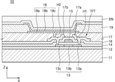
도 10은 도 9에 나타난 증착용 마스크를 포함하는 표시 장치 제조 장치를 개략적으로 나타내는 개념도이고, 도 11은 도 10에 나타난 표시 장치 제조 장치를 통하여 제조된 표시 장치의 일부를 나타내는 단면도이다.FIG. 10 is a conceptual diagram schematically illustrating an apparatus for manufacturing a display device including the deposition mask shown in FIG. 9 , and FIG. 11 is a cross-sectional view illustrating a part of the display device manufactured through the apparatus for manufacturing the display shown in FIG. 10 .
도 10 및 도 11을 참조하면, 표시 장치 제조 장치(100)는 챔버(141), 마스크 프레임 조립체(130), 안착부(142), 증착원(150), 기판지지부(161) 및 비전부(162)를 포함할 수 있다. 이때, 마스크 프레임 조립체(130)는 증착용 마스크(200)가 안착되어 고정되는 프레임(120)을 포함할 수 있다. 상기와 같은 증착용 마스크(200)는 도 1 내지 도 9에 나타난 증착용 마스크 제조 방법에 의해 제조된다.10 and 11 , the display
챔버(141)는 내부에 공간이 형성될 수 있으며, 일부가 개방될 수 있다. 이때, 챔버(141)의 개방된 부분에는 게이트 벨브(141a) 등이 설치되어 개방된 부분을 개폐할 수 있다.The
안착부(142)에는 마스크 프레임 조립체(130)가 안착될 수 있다. 이때, 안착부(142)는 마스크 프레임 조립체(130)를 회전시키거나, 선형 운동시킬 수 있도록 구성될 수 있다.The
상기와 같은 표시 장치 제조 장치(100)는 제1 기판(11)을 지지한 상태에서 증착 물질을 제1 기판(11)에 증착할 수 있다. 다른 실시예로써, 제1 기판(11)과 증착원(150)이 서로 상대 운동함으로써 증착 물질을 제1 기판(11)에 증착하는 것도 가능하다. 다만, 이하에서는 설명의 편의를 위하여 제1 기판(11)을 지지시킨 상태에서 증착 물질을 제1 기판(11)에 증착시키는 경우를 중심으로 상세히 설명하기로 한다.The display
챔버(141)에는 압력조절부(170)가 연결될 수 있다. 이때, 압력조절부(170)는 챔버(141)와 연결되는 연결배관(171)과, 연결배관(171)에 설치되는 펌프(172)를 포함할 수 있다.A
상기와 같은 표시 장치 제조 장치(100)는 유기층, 무기층 또는 금속층 등을 제1 기판(11)과 같은 표시 장치 기판에 증착할 수 있다. 다만, 이하에서는 설명의 편의를 위하여 표시 장치 제조 장치(100)가 유기층을 증착하는 경우를 중심으로 상세히 설명하기로 한다.In the display
구체적으로 표시 장치 제조 장치(100)의 작동을 살펴보면, 외부로부터 제1 기판(11) 및 마스크 프레임 조립체(130)를 챔버(141) 내부로 장입하여 각각 기판지지부(161) 및 안착부(142)에 지지시킬 수 있다.Specifically, looking at the operation of the display
이후, 비전부(162)를 통하여 마스크 프레임 조립체(130)와 제1 기판(11)의 위치를 측정한 후, 안착부(142)를 조절하여 제1 기판(11)과 마스크 프레임 조립체(130)의 위치를 정렬할 수 있다. 이때, 비전부(162)는 마스크 프레임 조립체(130)와 제1 기판(11)을 촬영하는 카메라를 포함할 수 있다.Thereafter, after measuring the positions of the
마스크 프레임 조립체(130)와 제1 기판(11)의 위치를 정렬한 후, 증착원(150)을 가동하여 증착 물질을 기화 또는 승화시킬 수 있다. 이때, 증착 물질은 증착용 마스크(200)의 슬롯을 통하여 제1 기판(11)에 증착될 수 있다. 이후, 증착이 완료된 제1 기판(11)을 챔버(141)의 외부로 인출하여 다음 공정을 수행할 수 있다.After aligning the positions of the
한편, 도 11을 참조하면, 상기와 같은 표시 장치 제조 장치(100)는 중간층(18b)을 형성할 수 있다. 이후 중간층(18b) 상에 대향 전극(18c)을 형성한 후, 대향 전극(18c) 상에 박막 봉지층(EN) 또는 제2 기판(미도시)을 설치하여 표시 장치(10)를 제조할 수 있다.Meanwhile, referring to FIG. 11 , the display
구체적으로 상기와 같은 표시 장치(10)는 제1 기판(11) 및 발광부(미도시)를 포함할 수 있다. 또한, 표시 장치(10)는 상기 발광부의 상부에 형성되는 박막 봉지층(EN) 또는 상기 제2 기판을 포함할 수 있다. 이때, 상기 제2 기판은 일반적인 표시 장치에 사용되는 것과 동일 또는 유사하므로 상세한 설명은 생략하기로 한다. 또한, 이하에서는 설명의 편의를 위하여 표시 장치(10)가 박막 봉지층(EN)을 포함하는 경우를 중심으로 상세히 설명하기로 한다.Specifically, the
상기 발광부는 박막 트랜지스터(TFT)를 구비하고, 이들을 덮도록 패시베이션막(17)이 형성되며, 이 패시베이션막(17) 상에 유기 발광 소자(18)가 형성될 수 있다.The light emitting unit includes a thin film transistor (TFT), a
제1 기판(11)에는 유리 재질을 사용할 수 있는 데, 반드시 이에 한정되지 않으며, 플라스틱재를 사용할 수도 있으며, SUS, Ti과 같은 금속재를 사용할 수도 있다. 또한, 제1 기판(11)은 폴리이미드(PI, Polyimide)로 구성될 수도 있다. 이하에서는 설명의 편의를 위하여 제1 기판(11)이 유리 재질로 형성되는 경우를 중심으로 상세히 설명하기로 한다.A glass material may be used for the
제1 기판(11)의 상면에는 유기화합물 및/또는 무기화합물로 이루어진 버퍼층(12)이 더 형성되는 데, 이는 실리콘 옥사이드(SiOx(x≥1)), 실리콘 나이트라이드(SiNx(x≥1))로 형성될 수 있다.A
이러한 버퍼층(12) 상에 소정의 패턴으로 배열된 활성층(13)이 형성된 후, 활성층(13)은 게이트 절연층(14)에 의해 매립된다. 활성층(13)은 소스 영역(13a)과 드레인 영역(13c)을 갖고, 그 사이에 채널 영역(13b)을 더 포함한다.After the
이러한 활성층(13)은 다양한 물질을 함유하도록 형성될 수 있다. 예를 들면, 활성층(13)은 비정질 실리콘 또는 결정질 실리콘과 같은 무기 반도체 물질을 함유할 수 있다. 다른 예로서 활성층(13)은 산화물 반도체를 함유할 수 있다. 또 다른 예로서, 활성층(13)은 유기 반도체 물질을 함유할 수 있다. 다만, 이하에서는 설명의 편의를 위하여 활성층(13)이 비정질 실리콘으로 형성되는 경우를 중심으로 상세히 설명하기로 한다. The
이러한 활성층(13)은 버퍼층(12) 상에 비정질 실리콘막을 형성한 후, 이를 결정화하여 다결정질 실리콘막으로 형성하고, 이 다결정질 실리콘막을 패터닝하여 형성할 수 있다. 상기 활성층(13)은 구동 TFT(미도시), 스위칭 TFT(미도시) 등 TFT 종류에 따라, 그 소스 영역(13a) 및 드레인 영역(13c)이 불순물에 의해 도핑된다.The
게이트 절연층(14)의 상면에는 활성층(13)과 대응되는 게이트 전극(15)과 이를 매립하는 층간 절연층(16)이 형성된다. A
그리고, 층간 절연층(16)과 게이트 절연층(14)에 콘택홀(H1)을 형성한 후, 층간 절연층(16) 상에 소스 전극(17a) 및 드레인 전극(17b)을 각각 소스 영역(13a) 및 드레인 영역(13c)에 콘택되도록 형성한다. Then, after forming a contact hole H1 in the
이렇게 형성된 상기 박막 트랜지스터의 상부로는 패시베이션막(17)이 형성되고, 이 패시베이션막(17) 상부에 유기 발광 소자(18, OLED)의 화소 전극(18a)이 형성된다. 이 화소 전극(18a)은 패시베이션막(17)에 형성된 비아 홀(H2)에 의해 TFT의 드레인 전극(17b)에 콘택된다.A
상기 패시베이션막(17)은 무기물 및/또는 유기물, 단층 또는 2개층 이상으로 형성될 수 있는 데, 하부 막의 굴곡에 관계없이 상면이 평탄하게 되도록 평탄화막으로 형성될 수도 있는 반면, 하부에 위치한 막의 굴곡을 따라 굴곡이 가도록 형성될 수 있다. 그리고, 이 패시베이션막(17)은, 공진 효과를 달성할 수 있도록 투명 절연체로 형성되는 것이 바람직하다.The
패시베이션막(17) 상에 화소 전극(18a)을 형성한 후에는 이 화소 전극(18a) 및 패시베이션막(17)을 덮도록 화소정의막(19)이 유기물 및/또는 무기물에 의해 형성되고, 화소 전극(18a)이 노출되도록 개구된다.After the
그리고, 적어도 상기 화소 전극(18a) 상에 중간층(18b) 및 대향 전극(18c)이 형성된다.Then, an
화소 전극(18a)은 애노드 전극의 기능을 하고, 대향 전극(18c)은 캐소오드 전극의 기능을 하는 데, 물론, 이들 화소 전극(18a)과 대향 전극(18c)의 극성은 반대로 되어도 무방하다.The
화소 전극(18a)과 대향 전극(18c)은 상기 중간층(18b)에 의해 서로 절연되어 있으며, 중간층(18b)에 서로 다른 극성의 전압을 가해 유기 발광층에서 발광이 이뤄지도록 한다.The
중간층(18b)은 유기 발광층을 구비할 수 있다. 선택적인 다른 예로서, 중간층(18b)은 유기 발광층(organic emission layer)을 구비하고, 그 외에 공통층(미표기)으로써 정공 주입층(hole injection layer), 정공 수송층(hole transport layer), 전자 수송층(electron transport layer) 및 전자 주입층(electron injection layer) 중 적어도 하나를 더 구비할 수 있다.The
하나의 단위 화소는 복수의 부화소로 이루어지는데, 복수의 부화소는 다양한 색의 빛을 방출할 수 있다. 예를 들면 복수의 부화소는 각각 적색, 녹색 및 청색의 빛을 방출하는 부화소를 구비할 수 있고, 적색, 녹색, 청색 및 백색의 빛을 방출하는 부화소를 구비할 수 있다.One unit pixel includes a plurality of sub-pixels, and the plurality of sub-pixels may emit light of various colors. For example, each of the plurality of sub-pixels may include a sub-pixel emitting red, green, and blue light, and may include a sub-pixel emitting red, green, blue, and white light.
한편, 상기와 같은 박막 봉지층(EN)은 복수의 무기층들을 포함하거나, 무기층 및 유기층을 포함할 수 있다.Meanwhile, the thin film encapsulation layer EN as described above may include a plurality of inorganic layers or may include an inorganic layer and an organic layer.
박막 봉지층(EN)의 상기 유기층은 고분자로 형성되며, 바람직하게는 폴리에틸렌테레프탈레이트, 폴리이미드, 폴라카보네이트, 에폭시, 폴리에틸렌 및 폴리아크릴레이트 중 어느 하나로 형성되는 단일막 또는 적층막일 수 있다. 더욱 바람직하게는, 상기 유기층은 폴리아크릴레이트로 형성될 수 있으며, 구체적으로는 디아크릴레이트계 모노머와 트리아크릴레이트계 모노머를 포함하는 모노머 조성물이 고분자화된 것을 포함할 수 있다. 상기 모노머 조성물에 모노아크릴레이트계 모노머가 더 포함될 수 있다. 또한, 상기 모노머 조성물에 2,4,6-트리메틸벤조일포스핀옥시드(TPO)와 같은 공지의 광개시제가 더욱 포함될 수 있으나 이에 한정되는 것은 아니다.The organic layer of the thin film encapsulation layer EN is formed of a polymer, and preferably a single film or a laminate film formed of any one of polyethylene terephthalate, polyimide, polycarbonate, epoxy, polyethylene, and polyacrylate. More preferably, the organic layer may be formed of polyacrylate, and specifically may include a polymerized monomer composition including a diacrylate-based monomer and a triacrylate-based monomer. A monoacrylate-based monomer may be further included in the monomer composition. In addition, a known photoinitiator such as 2,4,6-trimethylbenzoylphosphine oxide (TPO) may be further included in the monomer composition, but is not limited thereto.
박막 봉지층(EN)의 상기 무기층은 금속 산화물 또는 금속 질화물을 포함하는 단일막 또는 적층막일 수 있다. 구체적으로, 상기 무기층은 SiNx, Al2O3, SiO2, TiO2 중 어느 하나를 포함할 수 있다.The inorganic layer of the thin film encapsulation layer EN may be a single layer or a multilayer layer including a metal oxide or a metal nitride. Specifically, the inorganic layer may include any one of SiNx, Al2O3, SiO2, and TiO2.
박막 봉지층(EN) 중 외부로 노출된 최상층은 유기 발광 소자에 대한 투습을 방지하기 위하여 무기층으로 형성될 수 있다.The uppermost layer exposed to the outside of the thin film encapsulation layer EN may be formed of an inorganic layer to prevent moisture permeation to the organic light emitting diode.
박막 봉지층(EN)은 적어도 2개의 무기층 사이에 적어도 하나의 유기층이 삽입된 샌드위치 구조를 적어도 하나 포함할 수 있다. 다른 예로서, 박막 봉지층(EN)은 적어도 2개의 유기층 사이에 적어도 하나의 무기층이 삽입된 샌드위치 구조를 적어도 하나 포함할 수 있다. 또 다른 예로서, 박막 봉지층(EN)은 적어도 2개의 무기층 사이에 적어도 하나의 유기층이 삽입된 샌드위치 구조 및 적어도 2개의 유기층 사이에 적어도 하나의 무기층이 삽입된 샌드위치 구조를 포함할 수도 있다. The thin film encapsulation layer EN may include at least one sandwich structure in which at least one organic layer is inserted between at least two inorganic layers. As another example, the thin film encapsulation layer EN may include at least one sandwich structure in which at least one inorganic layer is inserted between at least two organic layers. As another example, the thin film encapsulation layer EN may include a sandwich structure in which at least one organic layer is inserted between at least two inorganic layers and a sandwich structure in which at least one inorganic layer is inserted between at least two organic layers. .
박막 봉지층(EN)은 유기 발광 소자(18, OLED)의 상부로부터 순차적으로 제1 무기층, 제1 유기층, 제2 무기층을 포함할 수 있다. The thin film encapsulation layer EN may include a first inorganic layer, a first organic layer, and a second inorganic layer sequentially from an upper portion of the organic light emitting device 18 (OLED).
다른 예로서, 박막 봉지층(EN)은 유기 발광 소자(18, OLED)의 상부로부터 순차적으로 제1 무기층, 제1 유기층, 제2 무기층, 제2 유기층, 제 3 무기층을 포함할 수 있다. As another example, the thin film encapsulation layer EN may include a first inorganic layer, a first organic layer, a second inorganic layer, a second organic layer, and a third inorganic layer sequentially from an upper portion of the organic light emitting diode 18 (OLED). there is.
또 다른 예로서, 박막 봉지층(EN)은 상기 유기 발광 소자(18, OLED)의 상부로부터 순차적으로 제1 무기층, 제1 유기층, 제2 무기층, 상기 제2 유기층, 제 3 무기층, 제 3 유기층, 제 4 무기층을 포함할 수 있다. As another example, the thin film encapsulation layer EN may include a first inorganic layer, a first organic layer, a second inorganic layer, the second organic layer, a third inorganic layer, It may include a third organic layer and a fourth inorganic layer.
유기 발광 소자(18, OLED)와 제1 무기층 사이에 LiF를 포함하는 할로겐화 금속층이 추가로 포함될 수 있다. 상기 할로겐화 금속층은 제1 무기층을 스퍼터링 방식으로 형성할 때 상기 유기 발광 소자(18, OLED)가 손상되는 것을 방지할 수 있다.A metal halide layer including LiF may be further included between the organic light emitting device 18 (OLED) and the first inorganic layer. The metal halide layer may prevent the organic light emitting device 18 (OLED) from being damaged when the first inorganic layer is formed by sputtering.
제1 유기층은 제2 무기층 보다 면적이 좁게 할 수 있으며, 상기 제2 유기층도 제 3 무기층 보다 면적이 좁을 수 있다.The first organic layer may have a smaller area than the second inorganic layer, and the second organic layer may also have a smaller area than the third inorganic layer.
따라서, 표시 장치 제조 장치(100)는 정밀한 패턴의 형성이 가능하다. 또한, 표시 장치(10)는 선명한 이미지 구현이 가능하다.Accordingly, the display
이와 같이 본 발명은 도면에 도시된 일 실시예를 참고로 하여 설명하였으나 이는 예시적인 것에 불과하며 당해 분야에서 통상의 지식을 가진 자라면 이로부터 다양한 변형 및 실시예의 변형이 가능하다는 점을 이해할 것이다. 따라서, 본 발명의 진정한 기술적 보호 범위는 첨부된 특허청구범위의 기술적 사상에 의하여 정해져야 할 것이다.As described above, the present invention has been described with reference to one embodiment shown in the drawings, but it will be understood that various modifications and variations of the embodiments are possible therefrom by those of ordinary skill in the art. Accordingly, the true technical protection scope of the present invention should be determined by the technical spirit of the appended claims.
110: 전주용 몰드 130: 마스크 프레임 조립체
111: 제1 층 141: 챔버
112: 제2 층 141a: 게이트 벨브
112a: 패턴홈 150: 증착원
113: 포토레지스트층 161: 기판지지부
113a: 노광 영역 170: 압력조절부
113b: 포토레지스트 패턴 171: 연결배관
114: 포토마스크 172: 펌프
120: 프레임 200: 증착용 마스크110: mold for electric pole 130: mask frame assembly
111: first layer 141: chamber
112:
112a: pattern groove 150: evaporation source
113: photoresist layer 161: substrate support
113a: exposure area 170: pressure control unit
113b: photoresist pattern 171: connection pipe
114: photomask 172: pump
120: frame 200: mask for deposition
Claims (11)
상기 제2 층의 일면에 포토레지스트층을 도포하고, 노광 및 현상 공정을 거쳐 상기 포토레지스트층을 관통하도록 복수개의 포토레지스트 패턴을 가공하는 단계;
상기 복수개의 포토레지스트 패턴에 의해 노출되는 상기 제2 층의 일부를 식각하여 상기 제2 층에 복수개의 패턴홈을 가공하는 단계;
상기 포토레지스트층을 제거하여 전주용 몰드를 가공하는 단계;
상기 전주용 몰드의 상기 제2 층에 전극판을 접촉시키는 단계;
전주 도금(electro-forming)을 실시하여 상기 전주용 몰드의 상기 각 패턴홈들의 사이에 형성되는 공간에 상기 전극판으로부터 금속층을 성장시켜 증착용 마스크를 가공하는 단계; 및
상기 전극판으로부터 상기 증착용 마스크를 분리하는 단계;를 포함하는, 증착용 마스크 제조 방법.depositing a second layer on one side of the first layer;
applying a photoresist layer to one surface of the second layer, and processing a plurality of photoresist patterns to penetrate the photoresist layer through exposure and development processes;
processing a plurality of pattern grooves in the second layer by etching a portion of the second layer exposed by the plurality of photoresist patterns;
removing the photoresist layer to process a mold for electroforming;
contacting an electrode plate to the second layer of the mold for electric poles;
processing a deposition mask by performing electro-forming to grow a metal layer from the electrode plate in a space formed between the pattern grooves of the electroforming mold; and
Separating the deposition mask from the electrode plate; including, a deposition mask manufacturing method.
상기 제1 층은 부도체로 구성되는 것을 특징으로 하는, 증착용 마스크 제조 방법.According to claim 1,
The method for manufacturing a mask for deposition, characterized in that the first layer is composed of an insulator.
상기 제1 층은 유리(glass), 플라스틱 및 폴리이미드(polyimide) 중 하나 이상을 포함하는 것을 특징으로 하는, 증착용 마스크 제조 방법.3. The method of claim 2,
The method of claim 1, wherein the first layer includes at least one of glass, plastic, and polyimide.
상기 제2 층은 화학 기상 증착(chemical vapor deposition) 공정으로 형성되는 것을 특징으로 하는, 증착용 마스크 제조 방법.According to claim 1,
The method of claim 1 , wherein the second layer is formed by a chemical vapor deposition process.
상기 제2 층은 실리콘 나이트라이드(SiNx) 및 실리콘 옥사이드(SiOx) 중 하나 이상을 포함하는, 증착용 마스크 제조 방법.According to claim 1,
The second layer comprises at least one of silicon nitride (SiN x ) and silicon oxide (SiO x ).
상기 제2 층에 복수개의 패턴홈을 가공하는 단계는,
상기 복수개의 포토레지스트층에 의해 노출되는 상기 제2 층의 일부를 건식 식각(dry-etching)하는 것을 특징으로 하는, 증착용 마스크 제조 방법.According to claim 1,
The step of machining a plurality of pattern grooves in the second layer,
A method of manufacturing a mask for deposition, characterized in that dry-etching a portion of the second layer exposed by the plurality of photoresist layers.
상기 복수개의 포토레지스트 패턴을 가공하는 단계는,
상기 복수개의 포토레지스트 패턴의 두께 방향의 단면이 테이퍼(taper)지도록 형성되는 것을 특징으로 하는, 증착용 마스크 제조 방법.According to claim 1,
The step of processing the plurality of photoresist patterns,
The method for manufacturing a deposition mask, characterized in that the cross-sections of the plurality of photoresist patterns in the thickness direction are formed to be tapered.
상기 복수개의 포토레지스트 패턴의 단면은 상기 제2 층의 상기 일면에 접촉하는 하면에서 상기 하면과 반대면인 상면으로 갈수록 점점 넓어지는 것을 특징으로 하는, 증착용 마스크 제조 방법.8. The method of claim 7,
Cross-sections of the plurality of photoresist patterns gradually widen from a lower surface in contact with the one surface of the second layer toward an upper surface opposite to the lower surface.
상기 제2 층에 복수개의 패턴홈을 가공하는 단계는,
상기 복수개의 패턴홈의 두께 방향의 단면이 테이퍼(taper)지도록 형성되는 것을 특징으로 하는, 증착용 마스크 제조 방법.According to claim 1,
The step of machining a plurality of pattern grooves in the second layer,
A method for manufacturing a deposition mask, characterized in that the cross-sections of the plurality of pattern grooves in the thickness direction are formed to be tapered.
상기 복수개의 패턴홈의 단면은 상기 포토레지스트층과 접촉하는 상기 제2 층의 상기 일면에서 상기 제1 층과 접촉하는 상기 제2 층의 타면으로 갈수록 점점 좁아지는 것을 특징으로 하는, 증착용 마스크 제조 방법.10. The method of claim 9,
Cross-sections of the plurality of pattern grooves are gradually narrowed from one surface of the second layer in contact with the photoresist layer to the other surface of the second layer in contact with the first layer. method.
상기 증착용 마스크는,
상기 전주 도금(electro-forming)을 실시하여 상기 전주용 몰드의 상기 각 패턴홈들 사이에 형성되는 공간에 상기 전극판으로부터 금속층을 성장시켜 증착용 마스크를 가공하는 단계와, 상기 전극판으로부터 상기 증착용 마스크를 분리하는 단계를 반복적으로 수행함으로써 제조되는 것을 특징으로 하는, 증착용 마스크 제조 방법.According to claim 1,
The deposition mask is
processing a deposition mask by growing a metal layer from the electrode plate in a space formed between the respective pattern grooves of the electroforming mold by performing the electro-forming; A method of manufacturing a mask for deposition, characterized in that it is manufactured by repeatedly performing the step of separating the wearing mask.
Priority Applications (2)
| Application Number | Priority Date | Filing Date | Title |
|---|---|---|---|
| KR1020150139995A KR102378358B1 (en) | 2015-10-05 | 2015-10-05 | Method of manufacturing mask for deposition |
| US15/096,820 US9543520B1 (en) | 2015-10-05 | 2016-04-12 | Method of manufacturing mask for deposition |
Applications Claiming Priority (1)
| Application Number | Priority Date | Filing Date | Title |
|---|---|---|---|
| KR1020150139995A KR102378358B1 (en) | 2015-10-05 | 2015-10-05 | Method of manufacturing mask for deposition |
Publications (2)
| Publication Number | Publication Date |
|---|---|
| KR20170040862A KR20170040862A (en) | 2017-04-14 |
| KR102378358B1 true KR102378358B1 (en) | 2022-03-25 |
Family
ID=57706046
Family Applications (1)
| Application Number | Title | Priority Date | Filing Date |
|---|---|---|---|
| KR1020150139995A Expired - Fee Related KR102378358B1 (en) | 2015-10-05 | 2015-10-05 | Method of manufacturing mask for deposition |
Country Status (2)
| Country | Link |
|---|---|
| US (1) | US9543520B1 (en) |
| KR (1) | KR102378358B1 (en) |
Families Citing this family (3)
| Publication number | Priority date | Publication date | Assignee | Title |
|---|---|---|---|---|
| KR101986525B1 (en) * | 2018-08-29 | 2019-06-07 | 주식회사 티지오테크 | Producing method of mask |
| KR102129777B1 (en) * | 2019-05-13 | 2020-07-03 | 크레아퓨쳐 주식회사 | Manufacturing method of fine metal mask |
| CN114127338B (en) * | 2019-05-13 | 2022-12-09 | 创造未来有限公司 | Method for manufacturing mold for manufacturing fine metal mask and method for manufacturing fine metal mask |
Family Cites Families (7)
| Publication number | Priority date | Publication date | Assignee | Title |
|---|---|---|---|---|
| JP4072422B2 (en) * | 2002-11-22 | 2008-04-09 | 三星エスディアイ株式会社 | Deposition mask structure, method for producing the same, and method for producing organic EL element using the same |
| JP2005154879A (en) | 2003-11-28 | 2005-06-16 | Canon Components Inc | Metal mask for vapor deposition, and method of producing vapor deposition pattern using the same |
| KR100897509B1 (en) | 2007-04-24 | 2009-05-15 | 박태흠 | Micrometallic mold for producing a metal thin plate having an intaglio portion, an embossed portion and a penetrating portion, a manufacturing method thereof and a metal thin plate manufactured by the above fine metal mold |
| JP5178501B2 (en) | 2008-12-26 | 2013-04-10 | 株式会社ソノコム | Metal mask provided with recognition mark and method of manufacturing the same |
| KR101926580B1 (en) * | 2012-07-04 | 2018-12-10 | 엘지이노텍 주식회사 | Method for manufacturing Metal mask for large-area display |
| KR101468405B1 (en) | 2013-02-27 | 2014-12-10 | 주식회사 웨이브일렉트로닉스 | method for producing shadow mask for OLED fabrication by multiple exposure and electroplating |
| US9695522B2 (en) * | 2014-11-21 | 2017-07-04 | Samsung Display Co., Ltd. | Deposition mask, method of manufacturing deposition mask, and method of manufacturing display apparatus |
-
2015
- 2015-10-05 KR KR1020150139995A patent/KR102378358B1/en not_active Expired - Fee Related
-
2016
- 2016-04-12 US US15/096,820 patent/US9543520B1/en not_active Expired - Fee Related
Also Published As
| Publication number | Publication date |
|---|---|
| KR20170040862A (en) | 2017-04-14 |
| US9543520B1 (en) | 2017-01-10 |
Similar Documents
| Publication | Publication Date | Title |
|---|---|---|
| KR102404576B1 (en) | Mask frame assembly for thin layer deposition, manufacturing method of the same and manufacturing method of display device there used | |
| KR102420460B1 (en) | Mask frame assembly, apparatus and method for manufacturing a display apparatus | |
| KR102474208B1 (en) | A mask assembly, apparatus and method for manufacturing a display apparatus using the same | |
| KR102524534B1 (en) | mask for deposition, apparatus for manufacturing display apparatus and method of manufacturing display apparatus | |
| KR102608420B1 (en) | mask for deposition, apparatus for manufacturing display apparatus and method of manufacturing display apparatus | |
| US20200343322A1 (en) | Organic light emitting diode (oled) substrate and manufacturing method thereof, display device | |
| KR102552275B1 (en) | Manufacturing method for the mask | |
| US20110168087A1 (en) | Mask frame assembly for thin film deposition | |
| KR102424976B1 (en) | A mask assembly, apparatus and method for manufacturing a display apparatus using the same | |
| US20160035802A1 (en) | Light-emitting device, array substrate, display device and manufacturing method of light-emitting device | |
| KR20170053779A (en) | Mask frame assembly, apparatus for deposition comprising the same and method of manufacturing display apparatus | |
| KR20180032717A (en) | mask for deposition, apparatus for manufacturing display apparatus and method of manufacturing display apparatus | |
| US20170358746A1 (en) | Mask frame assembly for thin layer deposition, method of manufacturing the same, and method of manufacturing display apparatus by using the mask frame assembly | |
| KR102399569B1 (en) | Mask assembly, Apparatus for manufacturing display apparatus and method of manufacturing display apparatus | |
| KR102704441B1 (en) | mask for deposition, manufacturing method thereof, manufacturing apparatus of display apparatus and manufacturing method of display apparatus | |
| US10403860B2 (en) | Mask frame assembly, a method of manufacturing the same, and a method of manufacturing a display apparatus | |
| KR102388719B1 (en) | Mask for thin film deposition, method for manufacturing thereof, and method for manufacturing a display apparatus using the same | |
| KR20160046071A (en) | Mask assembly, Apparatus for manufacturing display apparatus and method of manufacturing display apparatus | |
| KR102309621B1 (en) | Mask frame assembly for deposition, manufacturing method of the same | |
| KR102378358B1 (en) | Method of manufacturing mask for deposition | |
| US20180315926A1 (en) | Apparatus and method of directly patterning high resolution active matrix organic light emitting diodes using high-resolution shadow mask | |
| KR20170066766A (en) | Method for manufacturing a mask assembly and method for manufacturing a display apparatus | |
| US11895902B2 (en) | Display device with device board and manufacturing method thereof | |
| KR20160123434A (en) | Mask assembly and manufacturing apparatus for a display apparatus using the same |
Legal Events
| Date | Code | Title | Description |
|---|---|---|---|
| PA0109 | Patent application |
St.27 status event code: A-0-1-A10-A12-nap-PA0109 |
|
| PG1501 | Laying open of application |
St.27 status event code: A-1-1-Q10-Q12-nap-PG1501 |
|
| P22-X000 | Classification modified |
St.27 status event code: A-2-2-P10-P22-nap-X000 |
|
| R18-X000 | Changes to party contact information recorded |
St.27 status event code: A-3-3-R10-R18-oth-X000 |
|
| A201 | Request for examination | ||
| PA0201 | Request for examination |
St.27 status event code: A-1-2-D10-D11-exm-PA0201 |
|
| E902 | Notification of reason for refusal | ||
| PE0902 | Notice of grounds for rejection |
St.27 status event code: A-1-2-D10-D21-exm-PE0902 |
|
| P11-X000 | Amendment of application requested |
St.27 status event code: A-2-2-P10-P11-nap-X000 |
|
| P13-X000 | Application amended |
St.27 status event code: A-2-2-P10-P13-nap-X000 |
|
| E701 | Decision to grant or registration of patent right | ||
| PE0701 | Decision of registration |
St.27 status event code: A-1-2-D10-D22-exm-PE0701 |
|
| GRNT | Written decision to grant | ||
| PR0701 | Registration of establishment |
St.27 status event code: A-2-4-F10-F11-exm-PR0701 |
|
| PR1002 | Payment of registration fee |
St.27 status event code: A-2-2-U10-U11-oth-PR1002 Fee payment year number: 1 |
|
| PG1601 | Publication of registration |
St.27 status event code: A-4-4-Q10-Q13-nap-PG1601 |
|
| P22-X000 | Classification modified |
St.27 status event code: A-4-4-P10-P22-nap-X000 |
|
| P22-X000 | Classification modified |
St.27 status event code: A-4-4-P10-P22-nap-X000 |
|
| P22-X000 | Classification modified |
St.27 status event code: A-4-4-P10-P22-nap-X000 |
|
| PC1903 | Unpaid annual fee |
St.27 status event code: A-4-4-U10-U13-oth-PC1903 Not in force date: 20250322 Payment event data comment text: Termination Category : DEFAULT_OF_REGISTRATION_FEE |
|
| H13 | Ip right lapsed |
Free format text: ST27 STATUS EVENT CODE: N-4-6-H10-H13-OTH-PC1903 (AS PROVIDED BY THE NATIONAL OFFICE); TERMINATION CATEGORY : DEFAULT_OF_REGISTRATION_FEE Effective date: 20250322 |
|
| PC1903 | Unpaid annual fee |
St.27 status event code: N-4-6-H10-H13-oth-PC1903 Ip right cessation event data comment text: Termination Category : DEFAULT_OF_REGISTRATION_FEE Not in force date: 20250322 |
|
| P22-X000 | Classification modified |
St.27 status event code: A-4-4-P10-P22-nap-X000 |