KR102378293B1 - Methoid of manufacturing touch sensor integrated type display device - Google Patents
Methoid of manufacturing touch sensor integrated type display device Download PDFInfo
- Publication number
- KR102378293B1 KR102378293B1 KR1020150152674A KR20150152674A KR102378293B1 KR 102378293 B1 KR102378293 B1 KR 102378293B1 KR 1020150152674 A KR1020150152674 A KR 1020150152674A KR 20150152674 A KR20150152674 A KR 20150152674A KR 102378293 B1 KR102378293 B1 KR 102378293B1
- Authority
- KR
- South Korea
- Prior art keywords
- touch
- electrode
- gate
- insulating layer
- disposed
- Prior art date
- Legal status (The legal status is an assumption and is not a legal conclusion. Google has not performed a legal analysis and makes no representation as to the accuracy of the status listed.)
- Active
Links
Images


Classifications
-
- G—PHYSICS
- G06—COMPUTING OR CALCULATING; COUNTING
- G06F—ELECTRIC DIGITAL DATA PROCESSING
- G06F3/00—Input arrangements for transferring data to be processed into a form capable of being handled by the computer; Output arrangements for transferring data from processing unit to output unit, e.g. interface arrangements
- G06F3/01—Input arrangements or combined input and output arrangements for interaction between user and computer
- G06F3/03—Arrangements for converting the position or the displacement of a member into a coded form
- G06F3/041—Digitisers, e.g. for touch screens or touch pads, characterised by the transducing means
- G06F3/0412—Digitisers structurally integrated in a display
-
- G—PHYSICS
- G06—COMPUTING OR CALCULATING; COUNTING
- G06F—ELECTRIC DIGITAL DATA PROCESSING
- G06F3/00—Input arrangements for transferring data to be processed into a form capable of being handled by the computer; Output arrangements for transferring data from processing unit to output unit, e.g. interface arrangements
- G06F3/01—Input arrangements or combined input and output arrangements for interaction between user and computer
- G06F3/03—Arrangements for converting the position or the displacement of a member into a coded form
- G06F3/041—Digitisers, e.g. for touch screens or touch pads, characterised by the transducing means
- G06F3/044—Digitisers, e.g. for touch screens or touch pads, characterised by the transducing means by capacitive means
-
- G—PHYSICS
- G06—COMPUTING OR CALCULATING; COUNTING
- G06F—ELECTRIC DIGITAL DATA PROCESSING
- G06F2203/00—Indexing scheme relating to G06F3/00 - G06F3/048
- G06F2203/041—Indexing scheme relating to G06F3/041 - G06F3/045
- G06F2203/04103—Manufacturing, i.e. details related to manufacturing processes specially suited for touch sensitive devices
Landscapes
- Engineering & Computer Science (AREA)
- General Engineering & Computer Science (AREA)
- Theoretical Computer Science (AREA)
- Human Computer Interaction (AREA)
- Physics & Mathematics (AREA)
- General Physics & Mathematics (AREA)
- Devices For Indicating Variable Information By Combining Individual Elements (AREA)
- Liquid Crystal (AREA)
Abstract
본 발명은 터치센서 내장형 표시장치 및 그 제조방법에 관한 것으로, 터치센서 내장형 표시장치는 서로 교차하도록 배치되는 복수의 게이트 라인들 및 복수의 데이터 라인들, 복수의 화소전극들, 복수의 터치/공통전극, 및 라우팅 배선들을 포함한다. 화소전극들 각각은 제 1 줄기부와, 상기 제 1 줄기부로부터 분기되어 상기 화소영역으로 연장되는 복수의 제 1 가지부들을 구비한다. 터치/공통전극들 각각은 상기 복수의 화소전극들과 동일층에 배치되며, 제 2 줄기부와 상기 제 2 줄기부로부터 분기되어 상기 화소영역으로 연장되며, 상기 복수의 제 1 가지부들과 번갈아 배치되는 복수의 제 2 가지부들을 구비한다. 라우팅 배선들은 상기 복수의 터치/공통전극에 각각 연결된다. The present invention relates to a touch sensor embedded display device and a method for manufacturing the same, wherein the touch sensor embedded display device includes a plurality of gate lines and a plurality of data lines, a plurality of pixel electrodes, and a plurality of touch/common lines disposed to cross each other. electrodes, and routing wires. Each of the pixel electrodes includes a first stem portion and a plurality of first branch portions branching from the first stem portion and extending into the pixel region. Each of the touch/common electrodes is disposed on the same layer as the plurality of pixel electrodes, a second stem is branched from the second stem and extends into the pixel area, and is alternately disposed with the plurality of first branches. and a plurality of second branch portions that become The routing wires are respectively connected to the plurality of touch/common electrodes.
Description
본 발명은 터치센서 내장형 표시장치 및 그 제조방법에 관한 것이다. The present invention relates to a touch sensor-embedded display device and a method for manufacturing the same.
최근, 멀티미디어의 발달과 함께 이를 적절하게 표시할 수 있는 표시장치의 필요성에 부합하여, 대형화가 가능하고, 가격이 저렴하면서, 높은 표시품질(동영상 표현력, 해상도, 밝기, 명암비, 및 색 재현력 등)을 갖는 평면형 표시장치(이하, 간단히 "표시장치"라 함)의 개발이 진행되고 있다. 이들 평면형 표시장치에는 키보드, 마우스, 트랙볼, 조이스틱, 디지타이저(digitizer) 등의 다양한 입력장치(Input Device)들이 사용자와 표시장치 사이의 인터페이스를 구성하기 위해 사용되고 있다. Recently, along with the development of multimedia, in accordance with the need for a display device that can display it properly, it can be enlarged, and the price is low, and the display quality is high (video expression power, resolution, brightness, contrast ratio, color reproduction, etc.) Development of a flat-type display device (hereinafter, simply referred to as a “display device”) having Various input devices such as a keyboard, a mouse, a trackball, a joystick, and a digitizer are used in these flat display devices to form an interface between the user and the display device.
그러나, 상술한 바와 같은 입력장치를 사용하는 것은 사용법을 익혀야 하고 공간을 차지하는 등의 불편을 야기하여 제품의 완성도를 높이기 어려운 면이 있었다. 따라서, 편리하면서도 간단하고 오작동을 감소시킬 수 있는 표시장치용 입력장치에 대한 요구가 날로 증가되고 있다. 이와 같은 요구에 따라 사용자가 표시장치를 보면서 손이나 펜 등으로 화면을 직접 터치하거나 근접시켜 정보를 입력하면 이를 인식할 수 있는 터치센서(touch sensor)가 제안되었다. However, using the input device as described above causes inconvenience such as having to learn how to use and occupying space, so that it is difficult to improve the quality of the product. Accordingly, the demand for an input device for a display device that is convenient, simple, and capable of reducing malfunctions is increasing day by day. In response to such a request, a touch sensor capable of recognizing when a user directly touches or approaches a screen with a hand or a pen while looking at a display device and inputs information has been proposed.
터치센서는 간단하고, 오작동이 적으며, 별도의 입력기기를 사용하지 않고도 입력이 가능할 뿐 아니라 사용자가 화면에 표시되는 내용을 통해 신속하고 용이하게 조작할 수 있다는 편리성 때문에 다양한 표시장치에 적용되고 있다. The touch sensor is applied to various display devices because it is simple, has few malfunctions, can input without using a separate input device, and allows the user to quickly and easily manipulate the contents displayed on the screen. there is.
상술한 표시장치에 사용되는 터치센서는 그 구조에 따라 상판 부착형(add-on type), 상판 일체형(on-cell type) 및 내장형(integrated type 또는 in-cell type)으로 나눌 수 있다. 상판 부착형은 표시장치와 터치센서 모듈을 개별적으로 제조한 후에, 표시장치의 상판에 터치센서 모듈을 부착하는 방식이다. 상판 일체형은 표시장치의 상부 유리 기판 표면에 터치센서 소자들을 직접 형성하는 방식이다. 내장형은 표시장치 내부에 터치센서 소자들을 내장하여 표시장치의 박형화를 달성하고 내구성을 높일 수 있는 방식이다.The touch sensor used in the above-described display device may be divided into an add-on type, an on-cell type, and an integrated type or an in-cell type, depending on the structure thereof. The top plate attachment type is a method in which the touch sensor module is attached to the top plate of the display device after the display device and the touch sensor module are separately manufactured. The integrated top plate is a method of directly forming the touch sensor elements on the surface of the upper glass substrate of the display device. The built-in type is a method in which touch sensor elements are embedded in the display device to achieve thinness of the display device and increase durability.
이들 중 상판 부착형 및 상판 일체형은 터치성능은 우수하나 두께의 증가, 화질저하(모아레 현상 또는 반사시감 등), 및 낮은 수율 등의 문제점이 있다. Among them, the top plate attachment type and the top plate integrated type have excellent touch performance, but have problems such as increase in thickness, deterioration of image quality (moiré phenomenon or reflection sense, etc.), and low yield.
반면 내장형 터치센서는 표시장치의 공통전극을 터치센서의 전극으로 공용할 수 있어 두께를 얇게 할 수 있고, 터치소자가 표시장치의 내부에 형성되므로 내구성을 높일 수 있다. On the other hand, the built-in touch sensor can share the common electrode of the display device as an electrode of the touch sensor, so that the thickness can be reduced, and durability can be improved because the touch device is formed inside the display device.
따라서, 내장형 터치센서는 내구성을 향상시키고 박형화가 가능하다는 점에서 상판 부착형 터치센서와 상판 일체형 터치센서의 단점을 해결할 수 있기 때문에 관심이 집중되고 있다. 이러한 내장형 터치센서는 터치된 부분을 감지하는 방식에 따라 광 방식과 정전용량 방식으로 구분되며, 정전용량 방식은 다시 자기 정전용량 방식(self capacitance type)과 상호 정전용량 방식(mutual capacitance type)으로 세분화된다. Therefore, the built-in touch sensor is attracting attention because it can solve the disadvantages of the top plate-attached touch sensor and the top plate-integrated touch sensor in terms of improving durability and reducing the thickness. These built-in touch sensors are divided into an optical method and a capacitive method according to the method of detecting the touched part, and the capacitive method is further subdivided into a self capacitance type and a mutual capacitance type. do.
자기 정전용량 방식 터치센서는 터치 감지 패널의 터치 영역에 복수의 독립 패턴을 형성하고 각각의 독립 패턴의 정전용량의 변화를 측정하여 터치 여부를 판단하는 방식이다. 상호 정전용량 방식 터치센서는 터치 감지 패널의 터치/공통전극 형성영역에 X축 전극라인들(예를 들면, 구동 전극라인들)과 Y축 전극라인들(예를 들면, 센싱 전극라인들)을 서로 교차시켜 매트릭스를 형성하고, X축 전극라인들에 구동펄스를 인가한 다음, Y축 전극라인들을 통해 X축 전극라인들과 Y축 전극라인들의 교차점으로 정의되는 센싱 노드들에 나타나는 전압의 변화를 감지하여 터치 여부를 판단하는 방식이다. The self-capacitance type touch sensor is a method of forming a plurality of independent patterns in a touch area of a touch sensing panel and measuring a change in capacitance of each independent pattern to determine whether a touch occurs. The mutual capacitance type touch sensor includes X-axis electrode lines (eg, driving electrode lines) and Y-axis electrode lines (eg, sensing electrode lines) in the touch/common electrode formation region of the touch sensing panel. A matrix is formed by crossing each other, and a driving pulse is applied to the X-axis electrode lines, and then the voltage change that appears at the sensing nodes defined by the intersection of the X-axis electrode lines and the Y-axis electrode lines through the Y-axis electrode lines. It is a method of determining whether a touch has been made by detecting
그러나, 상호 정전용량 방식 터치센서는 터치 인식시 발생하는 X축 전극라인들과 Y축 전극라인 사이의 상호 정전용량의 크기는 매우 작은 반면, 표시장치를 구성하는 게이트 라인과 데이터 라인에 의해 X축 전극라인들과 Y축 전극라인에 형성되는 기생 정전용량(parasitic capacitance)이 매우 커져 기생 정전용량에 의해 터치위치를 정확하게 인식하기 곤란한 문제점이 있다. However, in the mutual capacitance type touch sensor, the magnitude of the mutual capacitance between the X-axis electrode lines and the Y-axis electrode line generated during touch recognition is very small, whereas the X-axis is caused by the gate line and the data line constituting the display device. Since parasitic capacitance formed in the electrode lines and the Y-axis electrode line is very large, there is a problem in that it is difficult to accurately recognize a touch position due to the parasitic capacitance.
또한, 상호 정전용량 방식 터치센서는 멀티 터치 인식을 위해 공통전극 상에 터치 구동을 위한 다수의 터치 구동라인과 터치 센싱을 위한 다수의 터치 센싱라인을 형성시켜야 하기 때문에 매우 복잡한 배선구조를 필요로 하게 되는 문제점이 있다. In addition, the mutual capacitance type touch sensor requires a very complicated wiring structure because it is necessary to form a plurality of touch driving lines for touch driving and a plurality of touch sensing lines for touch sensing on a common electrode for multi-touch recognition. There is a problem being
자기 정전용량 방식 터치센서는 상호 정전용량 방식 터치센서에 비해 간단한 배선구조로 터치 정밀도를 높일 수 있으므로 필요에 따라 널리 사용되고 있다. The self-capacitance type touch sensor is widely used as necessary because it can increase the touch precision with a simple wiring structure compared to the mutual capacitance type touch sensor.
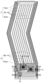
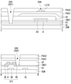
이하, 도 1 내지 도 3을 참조하여 종래의 자기 정전용량 방식 터치센서 내장형 액정 표시장치(이하, 단순히 "터치센서 내장형 표시장치"라 함)에 대해 설명하기로 한다. 도 1은 종래의 터치센서 내장형 표시장치를 도시한 평면도이다. 도 2는 도 1에 도시된 영역 R1에서 터치/공통전극과 화소전극의 관계를 도시한 평면도이고, 도 3은 도 2에서 데이터 라인 방향으로 배열되는 라우팅 배선과 그에 접속되는 터치/공통전극의 연결관계를 도시한 단면도이다.Hereinafter, a conventional self-capacitance type touch sensor embedded liquid crystal display device (hereinafter simply referred to as a "touch sensor embedded display device") will be described with reference to FIGS. 1 to 3 . 1 is a plan view illustrating a conventional touch sensor embedded display device. FIG. 2 is a plan view illustrating the relationship between the touch/common electrode and the pixel electrode in the region R1 shown in FIG. 1, and FIG. 3 is a routing wire arranged in the data line direction in FIG. 2 and the connection of the touch/common electrode connected thereto It is a cross-sectional view showing the relationship.
도 1을 참조하면, 터치센서 내장형 표시장치는 복수의 터치/공통전극들(T11~T14, T21~T24, T31~T34, T41~T44, T51~T54)과 복수의 라우팅 배선들(L11~L14, L21~L24, L31~L34, L41~L44, L51~L54)을 포함한다.1, the touch sensor built-in display device is a plurality of touch / common electrodes (T11 ~ T14, T21 ~ T24, T31 ~ T34, T41 ~ T44, T51 ~ T54) and a plurality of routing wires (L11 ~ L14) , L21 to L24, L31 to L34, L41 to L44, L51 to L54).
복수의 터치/공통전극들(T11~T14, T21~T24, T31~T34, T41~T44, T51~T54)은 표시영역에서 서로 교차하는 제 1 방향(예를 들면, x축 방향) 및 제 2 방향(예를 들면, y축 방향)으로 분할된다. 복수의 라우팅 배선들(L11~L14, L21~L24, L31~L34, L41~L44, L51~L54)은 복수의 터치/공통전극들(T11~T14, T21~T24, T31~T34, T41~T44, T51~T54)에 각각 연결되어 제 2 방향으로 서로 나란하게 배열된다. The plurality of touch/common electrodes T11 to T14, T21 to T24, T31 to T34, T41 to T44, and T51 to T54 intersect each other in a first direction (eg, an x-axis direction) and a second direction in the display area. direction (eg, the y-axis direction). A plurality of routing wires (L11 ~ L14, L21 ~ L24, L31 ~ L34, L41 ~ L44, L51 ~ L54) is a plurality of touch / common electrodes (T11 ~ T14, T21 ~ T24, T31 ~ T34, T41 ~ T44) , T51 to T54) and arranged in parallel with each other in the second direction.
복수의 터치/공통전극들(T11~T14, T21~T24, T31~T34, T41~T44, T51~T54)은 표시장치의 공통전극을 분할하여 형성된 것으로, 데이터를 표시하는 디스플레이 모드의 구동시에는 공통전극으로서 동작하고, 터치 위치를 인식하는 터치 구동시에는 터치/공통전극으로서 동작한다. The plurality of touch/common electrodes T11 to T14, T21 to T24, T31 to T34, T41 to T44, and T51 to T54 are formed by dividing the common electrode of the display device. It operates as a common electrode and operates as a touch/common electrode during touch driving to recognize a touch position.
소스 및 터치 구동 IC(10)는 디스플레이 구동시에는 표시장치의 게이트 라인들(도시생략)의 구동에 동기하여 데이터 라인들(도시 생략)에 표시 데이터를 공급하며, 터치/공통전극들(T11~T14, T21~T24, T31~T34, T41~T44, T51~T54)에 공통전압을 공급한다. 소스 및 터치구동 IC(10)는 또한 터치 구동시에는 터치/공통전극들에 터치 구동전압을 공급하고, 터치 전후의 터치/공통전극의 정전용량의 변화를 스캐닝하여 터치가 수행된 터치/공통전극의 위치를 결정한다. The source and touch driving IC 10 supplies display data to data lines (not shown) in synchronization with driving of gate lines (not shown) of the display device when driving the display, and touch/common electrodes T11 to T11 to A common voltage is supplied to T14, T21 to T24, T31 to T34, T41 to T44, and T51 to T54). The source and touch driving IC 10 also supplies a touch driving voltage to the touch/common electrodes during touch driving, and scans the change in capacitance of the touch/common electrode before and after the touch to perform the touch/common electrode. determine the location of
종래의 터치센서 내장형 표시장치는 또한 게이트 라인들 및 데이터 라인들을 포함하는 각종 배선들을 포함한다. The conventional touch sensor embedded display device also includes various wirings including gate lines and data lines.
도 2를 참조하면, 종래의 터치센서 내장형 표시장치에서는 터치/공통전극들(T11, T12, T21, T22) 각각에 대응하여 3행 3열로 배치된 9개의 화소전극들(P11~P33, P14-P36, P41~P63, P44~P66)이 배치되어 있다. 화소전극들(P11~P33, P14-P36, P41~P63, P44~P66)은 제 1 방향(예를 들면, x축 방향)으로 배열되는 복수의 게이트 라인들(G1~G6)과, 제 1 방향과 교차하는 제 2 방향(예를 들면, y축 방향)으로 배열되는 복수의 데이터 라인들(D1~D6)에 의해 정의되는 영역에 배치된다. 터치/공통전극들(T11, T12, T21, T22)에는 라우팅 배선들(L11, L12, L21, L22)이 각각 접속된다. 라우팅 배선들(L11, L12, L21, L22)은 제 2 방향을 따라 연장되어 소스 및 터치구동 IC(10)에 접속된다. Referring to FIG. 2 , in the conventional touch sensor embedded display device, nine pixel electrodes P11 to P33, P14- arranged in 3 rows and 3 columns corresponding to the touch/common electrodes T11, T12, T21, and T22, respectively. P36, P41 to P63, and P44 to P66) are arranged. The pixel electrodes P11 to P33, P14 to P36, P41 to P63, and P44 to P66 include a plurality of gate lines G1 to G6 arranged in a first direction (eg, an x-axis direction), and a first It is disposed in a region defined by a plurality of data lines D1 to D6 arranged in a second direction (eg, y-axis direction) intersecting the direction. Routing wires (L11, L12, L21, L22) are respectively connected to the touch/common electrodes (T11, T12, T21, T22). The routing wires L11 , L12 , L21 , and L22 extend along the second direction and are connected to the source and the
도 2 및 도 3을 참조하면, 기판(SUB1) 상에는 복수의 게이트 라인들(G1~G6)이 제 1 방향으로 배치되며, 그 상부에는 복수의 게이트 라인들(G1~G6)을 커버하도록 게이트 절연막(GI)이 배치된다. 게이트 절연막(GI) 상에서는 박막 트랜지스터(TFT)를 구성하는 활성층(A), 소스 전극(SE) 및 드레인 전극(DE)이 배치된다. 박막 트랜지스터(TFT)는 기판(SUB1) 상에 배치되는 게이트 라인들(G1~G6)로부터 각각 연장되는 게이트 전극들(GE)과, 게이트 라인들(G1~G6) 및 게이트 전극들(GE)을 커버하는 게이트 절연막(GI) 상에서 게이트 전극(GE)과 대응하는 영역에 배치되는 활성층(A)과, 활성층(A)의 일부를 노출시키도록 게이트 절연막(GI) 상에서 분리되어 배치되는 소스 전극(SE) 및 드레인 전극(DE)을 포함한다. 소스 전극(S)은 데이터 라인들(D1~D6) 각각으로부터 연장될 수 있다.2 and 3 , a plurality of gate lines G1 to G6 is disposed on a substrate SUB1 in a first direction, and a gate insulating layer is disposed on the substrate SUB1 to cover the plurality of gate lines G1 to G6 . (GI) is placed. An active layer A, a source electrode SE, and a drain electrode DE constituting the thin film transistor TFT are disposed on the gate insulating layer GI. The thin film transistor TFT includes gate electrodes GE respectively extending from the gate lines G1 to G6 disposed on the substrate SUB1, the gate lines G1 to G6, and the gate electrodes GE. The active layer A disposed in a region corresponding to the gate electrode GE on the covering gate insulating layer GI, and the source electrode SE disposed separately on the gate insulating layer GI to expose a portion of the active layer A ) and a drain electrode DE. The source electrode S may extend from each of the data lines D1 to D6.
박막 트랜지스터들(TFT)과 데이터 라인들(D1~D6)이 배치된 게이트 절연막(GI) 상에는 이들을 커버하는 제 1 절연막(IND1)과, 평탄화를 위한 제 2 절연막(INS2)이 순차적으로 배치된다. 제 2 절연막(INS2) 상에는 제 1 및 제 2 절연막(IND1, INS2)을 관통하는 콘택홀(CH1)을 통해 박막 트랜지스터들(TFT)의 드레인 전극들(DE)과 각각 접속되도록 화소전극들(P11~P66)이 배치된다. A first insulating layer IND1 covering the thin film transistors TFT and the data lines D1 to D6 is disposed on the gate insulating layer GI, and a second insulating layer INS2 for planarization is sequentially disposed. On the second insulating layer INS2 , the pixel electrodes P11 are respectively connected to the drain electrodes DE of the thin film transistors TFT through the contact hole CH1 passing through the first and second insulating layers IND1 and INS2 . ~P66) is placed.
제 2 절연막(INS2) 상에는 화소전극들(P11~P66)을 커버하도록 제 1 패시베이션막(PAD1)이 배치된다. 제 1 패시베이션막(PAD1) 상에는 터치 및 공통전극들(T11, T12, T21, T22)에 각각 연결될 라우팅 배선들(L11, L12, L21, L22)이 제 2 방향으로 배열된다.A first passivation layer PAD1 is disposed on the second insulating layer INS2 to cover the pixel electrodes P11 to P66. The routing wires L11, L12, L21, L22 to be respectively connected to the touch and common electrodes T11, T12, T21, and T22 are arranged on the first passivation film PAD1 in the second direction.
제 1 패시베이션막(PAD1) 상에는 라우팅 배선들(L11, L12, L21, L22)을 커버하도록 제 2 패시베이션막(PAS2)이 배치된다. 제 2 패시베이션막(PAS2) 상에는 화소전극들(P11~P33, P14~P36, P41~P63, P44~P66)과 각각 중첩되도록 터치/공통전극들(T11, T12, T21, T22)이 배치된다. 터치/공통전극들(T11, T12, T21, T22)은 제 2 패시베이션막(PAS2)을 관통하는 콘택홀들(CH2)을 통해 라우팅 배선들(L11, L12, L21, L22)에 각각 접속된다. 터치/공통전극들(T11, T12, T21, T22)은 화소전극들(P11~P33, P14~P36, P41~P63, P44~P66)과 프린지 필드(fringe field)를 형성하도록 화소영역 내에서 복수의 개구부를 갖거나 가지부를 갖도록 형성된다.A second passivation film (PAS2) is disposed on the first passivation film (PAD1) to cover the routing wires (L11, L12, L21, L22). Touch/common electrodes T11, T12, T21, and T22 are disposed on the second passivation layer PAS2 to overlap the pixel electrodes P11 to P33, P14 to P36, P41 to P63, and P44 to P66, respectively. The touch/common electrodes T11 , T12 , T21 , and T22 are respectively connected to the routing wires L11 , L12 , L21 , and L22 through the contact holes CH2 passing through the second passivation film PAS2 . The touch/common electrodes T11, T12, T21, and T22 are plural in the pixel area to form a fringe field with the pixel electrodes P11 to P33, P14 to P36, P41 to P63, and P44 to P66. It is formed to have an opening of or to have a branch portion.
다음으로 도 4a 내지 도 4c를 참조하여, 종래의 터치센서 내장형 표시장치에 터치가 행해졌을 경우, 단위 화소영역에서 발생하는 총 정전용량에 대해 검토해 보기로 한다. 도 4a는 종래의 터치센서 내장형 표시장치의 단위 화소영역에서 화소전극과 터치/공통전극만을 개략적으로 도시한 평면도이다. 도 4b는 도 4a의 I-I' 라인을 따라 취한 개략적 단면도이고, 도 4c는 도 4b의 단위 화소영역에서 터치에 의해 생성되는 정전용량 성분들을 개념적으로 도시한 등가 회로도이다.Next, with reference to FIGS. 4A to 4C , when a touch is applied to a conventional touch sensor embedded display device, a total capacitance generated in a unit pixel area will be reviewed. 4A is a plan view schematically illustrating only a pixel electrode and a touch/common electrode in a unit pixel area of a conventional touch sensor embedded display device. 4B is a schematic cross-sectional view taken along line I-I' of FIG. 4A, and FIG. 4C is an equivalent circuit diagram conceptually illustrating capacitance components generated by touch in the unit pixel area of FIG. 4B.
도 4a 내지 도 4c를 참조하면, 종래의 터치센서 내장형 표시장치에 예를 들면 손가락(F)으로 터치가 행해졌을 경우, 터치에 의한 정전용량 성분은 화소전극(P)과 손가락(F) 사이의 제 1 정전용량(Cpf)과 터치/공통전극(T)과 손가락 사이의 제 2 정전용량(Ctf)을 포함한다. Referring to FIGS. 4A to 4C , when a touch is performed with, for example, a finger F in a conventional touch sensor-embedded display device, the capacitance component due to the touch is formed between the pixel electrode P and the finger F. The first capacitance Cpf and the second capacitance Ctf between the touch/common electrode T and the finger are included.
도 4b에 도시된 바와 같이 제 1 정전용량(Cpf)은 손가락(F)과 화소전극(P) 사이의 정전용량이므로, 화소전극(P)과 손가락(F) 사이에 형성되는 제 1 서브-정전용량들(Cpf1+Cpf2+Cpf3+Cpf4)의 합이다. 따라서, 제 1 정전용량(Cpf)의 값은 다음과 같이 된다.As shown in FIG. 4B , the first capacitance Cpf is the capacitance between the finger F and the pixel electrode P, and thus the first sub-capacitance formed between the pixel electrode P and the finger F Sum of capacitances (Cpf1+Cpf2+Cpf3+Cpf4). Accordingly, the value of the first capacitance Cpf becomes as follows.
Cpf= Cpf1+Cpf2+ Cpf3+ Cpf4Cpf= Cpf1+Cpf2+ Cpf3+ Cpf4
또한 제 2 정전용량(Ctf)은 손가락(F)과 터치/공통전극(T) 사이의 정전용량이므로, 화소전극(P)의 개구부들(또는 핑거부들)을 통해 노출되는 터치/공통전극(T)과 손가락(F) 사이에 형성되는 제 2 서브-정전용량들(Ctf1+Ctf2+ Ctf3+ Ctf4+Ctf5)의 합이다. 따라서, 제 2 정전용량(Ctf)의 값은 다음과 같이 된다.Also, since the second capacitance Ctf is a capacitance between the finger F and the touch/common electrode T, the touch/common electrode T exposed through the openings (or fingers) of the pixel electrode P ) and the second sub-capacitances Ctf1+Ctf2+Ctf3+Ctf4+Ctf5 formed between the finger F. Accordingly, the value of the second capacitance Ctf becomes as follows.
Ctf= Ctf1+Ctf2+ Ctf3+ Ctf4+Ctf5Ctf= Ctf1+Ctf2+ Ctf3+ Ctf4+Ctf5
도 4a에 도시된 단위 화소영역 내의 화소전극(P) 및 터치/공통전극(T)에서, 4개의 가지부들(Pbr)을 갖는 화소전극(P)의 각 가지부(Pbr)의 폭 및 가지부들(Pbr) 사이의 간격이 각각 4㎛이고, 이러한 화소전극(P)과 중첩되는 장방형 터치/공통전극(T) 1 변의 폭이 36㎛, 다른 1변의 폭이 100㎛로 하고, 터치 후의 상태를 시뮬레이션한 결과, 제 1 서브-정전용량들(Cpf1, Cpf2, Cpf3, Cpf4)과 제 2 서브-정전용량들(Ctf1, Ctf2, Ctf3, Ctf4, Ctf5)은 다음의 값을 갖게 되었다.In the pixel electrode P and the touch/common electrode T in the unit pixel area shown in FIG. 4A , the width and branch portions of each branch portion Pbr of the pixel electrode P having four branch portions Pbr (Pbr) each 4㎛, the width of one side of the rectangular touch/common electrode (T) overlapping the pixel electrode (P) is 36㎛, the other side is 100㎛, the state after the touch As a result of the simulation, the first sub-capacitances Cpf1, Cpf2, Cpf3, and Cpf4 and the second sub-capacitances Ctf1, Ctf2, Ctf3, Ctf4, and Ctf5 have the following values.
Cpf1=29fF, Cpf2=29fF, Cpf3=29fF, Cpf4=29fFCpf1=29fF, Cpf2=29fF, Cpf3=29fF, Cpf4=29fF
Ctf1=0.544fF, Ctf2=0.544fF, Ctf3=0.544fF, Ctf4=0.544fF, Ctf5=0.544fFCtf1=0.544fF, Ctf2=0.544fF, Ctf3=0.544fF, Ctf4=0.544fF, Ctf5=0.544fF
따라서, 제 1 서브-정전용량의 합 Cpf=Cpf1+Cpf2+Cpf3+Cpf4=116fF로 되고, 제 2 서브-정전용량 Ctf=Ctf1+Ctf2+Ctf3+Ctf4+Ctf5=2.72fF로 되어 총 정전용량은 Cto1=Cpf+Ctf=118.72fF로 된다. Therefore, the sum of the first sub-capacitance Cpf = Cpf1 + Cpf2 + Cpf3 + Cpf4 = 116fF, the second sub-capacitance Ctf = Ctf1 + Ctf2 + Ctf3 + Ctf4 + Ctf5 = 2.72fF, so that the total capacitance is Cto1 = Cpf + Ctf = 118.72fF.
상술한 바와 같이 손가락(F)과 화소전극(P) 사이의 제 1 정전용량은 118.72fF이고, 터치/공통전극(T)과 손가락(F) 사이에 형성되는 제 2 정전용량은 2.72fF 로 제 2 정전용량의 값이 제 1 정전용량의 값보다 훨씬 작다. 이는 화소전극(P)이 손가락과 터치/공통전극(T) 사이에 형성되는 전계를 차폐하는 것에 기인한 것으로, 이러한 전계 차폐로 인해 제 2 정전용량의 부족한 값은 터치센싱 감도르 저하시키는 원이이 되었다.As described above, the first capacitance between the finger F and the pixel electrode P is 118.72 fF, and the second capacitance formed between the touch/common electrode T and the finger F is 2.72 fF. The value of the second capacitance is much smaller than the value of the first capacitance. This is due to the pixel electrode (P) shielding the electric field formed between the finger and the touch/common electrode (T). .
다음으로 도 4d를 참조하여 종래의 터치센서 내장형 표시장치의 광 투과도에 대해 검토해 보기로 한다. 도 4d는 도 4a의 I-I' 라인을 따라 취한 단면도로서, 광이 투과되는 영역을 개념적으로 도시한 단면도이다. Next, with reference to FIG. 4D , the light transmittance of the conventional touch sensor embedded display device will be reviewed. FIG. 4D is a cross-sectional view taken along line I-I' of FIG. 4A, and is a cross-sectional view conceptually illustrating a region through which light is transmitted.
도 4d를 참조하면, 종래의 터치센서 내장형 표시장치의 투과율은 화소전극(P)의 개구부, 즉 터치/공통전극(T)과 화소전극(P)의 비중첩부에 가장 많은 영향을 받게 된다. 그러나, 도 4d에 도시된 바와 같이, 종래의 터치센서 내장형 표시장치에서는 데이터 라인과 화소전극 사이의 간섭을 방지하기 위해 데이터 라인에 인접한 화소영역의 최 외각부는 터치/공통전극(T)이 확장된 구조로 되어 있다. 또한, 터치/공통전극(P)과 그에 인접한 데이터 라인 사이에 커플링 정전용량, 즉 기생 정전용량 발생하면 화질에 악영향을 미치므로, 이를 방지하기 위해 터치/공통전극(P)과 그에 인접한 데이터 라인 사이에는 터치/공통전극(T)과 중첩되도록 블랙매트릭스가 배치된다.Referring to FIG. 4D , the transmittance of the conventional touch sensor embedded display device is most affected by the opening of the pixel electrode P, that is, the non-overlapping portion of the touch/common electrode T and the pixel electrode P. However, as shown in FIG. 4D , in the conventional touch sensor-embedded display device, in order to prevent interference between the data line and the pixel electrode, the outermost portion of the pixel region adjacent to the data line has the touch/common electrode T extended. is structured. In addition, when coupling capacitance, that is, parasitic capacitance, occurs between the touch/common electrode P and the data line adjacent thereto, it adversely affects the image quality. To prevent this, the touch/common electrode P and the data line adjacent thereto A black matrix is disposed therebetween so as to overlap the touch/common electrode T.
따라서, 종래의 터치센서 내장형 표시장치에서는 투과영역의 면적이 줄어들어 개구율을 향상시키기 위한 대책이 필요하게 되었다. Accordingly, in the conventional display device with a built-in touch sensor, the area of the transmission region is reduced, so a countermeasure for improving the aperture ratio is required.
본 발명은 상술한 문제점을 해소시키기 위한 것으로, 터치시 손가락 등의 터치 객체와 화소전극 및 터치/공통전극 사이의 정전용량을 증가시켜 터치 정밀도를 향상시키는 동시에, 개구율을 높여 광 투과율을 향상시킴으로써 표시품질을 높일 수 있는 터치센서 내장형 표시장치와 그 제조방법을 제공하기 위한 것이다.The present invention is to solve the above problems, and at the time of touch, increase the capacitance between a touch object such as a finger and a pixel electrode and a touch/common electrode to improve touch precision, and at the same time improve the light transmittance by increasing the aperture ratio. An object of the present invention is to provide a display device with a built-in touch sensor capable of improving quality and a method for manufacturing the same.
상기 목적 달성을 위한 본 발명에 따르는 터치센서 내장형 표시장치는 서로 교차하도록 배치되는 복수의 게이트 라인들 및 복수의 데이터 라인들, 복수의 화소전극들, 복수의 터치/공통전극, 및 라우팅 배선들을 포함한다. 화소전극들 각각은 제 1 줄기부와, 상기 제 1 줄기부로부터 분기되어 상기 화소영역으로 연장되는 복수의 제 1 가지부들을 구비한다. 터치/공통전극들 각각은 상기 복수의 화소전극들과 동일층에 배치되며, 제 2 줄기부와 상기 제 2 줄기부로부터 분기되어 상기 화소영역으로 연장되며, 상기 복수의 제 1 가지부들과 번갈아 배치되는 복수의 제 2 가지부들을 구비한다. 라우팅 배선들은 상기 복수의 터치/공통전극에 각각 연결된다.A display device with a built-in touch sensor according to the present invention for achieving the above object includes a plurality of gate lines and a plurality of data lines, a plurality of pixel electrodes, a plurality of touch/common electrodes, and routing wires disposed to cross each other do. Each of the pixel electrodes includes a first stem portion and a plurality of first branch portions branching from the first stem portion and extending into the pixel region. Each of the touch/common electrodes is disposed on the same layer as the plurality of pixel electrodes, a second stem is branched from the second stem and extends into the pixel area, and is alternately disposed with the plurality of first branches. and a plurality of second branch portions that become The routing wires are respectively connected to the plurality of touch/common electrodes.
상기 구성에서, 서로 인접한 2개의 데이터 라인들 사이에 배치된 상기 제 1 가지부들과 제 2 가지부들 중 상기 서로 인접한 2개의 데이터 라인들에 가장 근접한 가지부는 제 2 가지부들이다. In the above configuration, among the first and second branches disposed between the two data lines adjacent to each other, the branch closest to the two data lines adjacent to each other is the second branch parts.
또한, 상기 복수의 라우팅 배선들은 상기 복수의 데이터 라인과 각각 중첩되고, 상기 제 2 가지부의 적어도 일부분과 중첩되도록 배열된다.In addition, the plurality of routing wires overlap the plurality of data lines, respectively, and are arranged to overlap at least a portion of the second branch portion.
또한, 상기 표시영역 내에서 상기 복수의 라우팅 배선들의 길이는 동일할 수 있다.In addition, the length of the plurality of routing wires in the display area may be the same.
또한, 상기 복수의 라우팅 배선들의 각각은 하부 금속층, 상기 하부 금속층 상에 배치되는 하나의 저저항 금속층, 및 상기 저저항 금속층 상에 배치되는 상부 금속층으로 이루어질 수 있다.In addition, each of the plurality of routing wires may be made of a lower metal layer, one low-resistance metal layer disposed on the lower metal layer, and an upper metal layer disposed on the low-resistance metal layer.
또한, 상기 상부 금속층은 상기 저저항 금속층 및 상기 하부 금속층을 커버하도록 배치될 수 있다.Also, the upper metal layer may be disposed to cover the low resistance metal layer and the lower metal layer.
또한, 상기 상부 금속층은 상기 저저항 금속층 및 상기 하부 금속층의 측면을 노출시킬 수 있다.In addition, the upper metal layer may expose side surfaces of the low resistance metal layer and the lower metal layer.
또한, 터치센서 내장형 표시장치는 기판 상에 배열되는 상기 게이트 라인 및 게이트 전극; 상기 게이트 라인 및 게이트 전극을 커버하는 게이트 절연막 상에 배치되는 박막 트랜지스터의 반도체층, 소스전극 및 드레인전극과, 상기 소스 전극에 연결된 상기 데이터 라인; 상기 박막 트랜지스터 및 데이터 라인을 커버하는 제 1 절연막, 및 상기 제 1 절연막 상의 각 화소영역에 배치되는 컬러필터; 상기 컬러필터 상에 순차적으로 배치되는 제 2 절연막 및 제 1 패시베이션막과, 상기 제 1 패시베이션막 상에 배치되는 상기 복수의 화소전극들 및 상기 복수의 터치/공통전극들; 및 상기 복수의 라우팅 배선들을 커버하는 제 2 패시베이션막 상에 배치되는 상기 복수의 라우팅 배선들을 포함할 수 있다. In addition, the touch sensor embedded display device includes the gate line and the gate electrode arranged on a substrate; a semiconductor layer, a source electrode and a drain electrode of a thin film transistor disposed on a gate insulating layer covering the gate line and the gate electrode, and the data line connected to the source electrode; a first insulating layer covering the thin film transistor and the data line, and a color filter disposed in each pixel area on the first insulating layer; a second insulating layer and a first passivation layer sequentially disposed on the color filter, and the plurality of pixel electrodes and the plurality of touch/common electrodes disposed on the first passivation layer; And it may include the plurality of routing wires disposed on the second passivation film covering the plurality of routing wires.
또한, 상기 라우팅 배선은 상기 제 2 패시베이션막을 관통하는 콘택홀을 통해 상기 터치/공통전극의 제 2 가지부에 접속되고, 상기 화소전극의 제 1 줄기부는 상기 제 1 패시베이션막, 제 2 절연막, 컬러필터 및 제 1 절연막을 관통하는 콘택홀을 통해 상기 박막 트랜지스터의 드레인 전극에 접속될 수 있다.In addition, the routing wiring is connected to the second branch portion of the touch/common electrode through a contact hole penetrating the second passivation film, and the first stem portion of the pixel electrode is the first passivation film, the second insulating film, the color It may be connected to the drain electrode of the thin film transistor through a contact hole passing through the filter and the first insulating layer.
또한, 본 발명의 터치센서 내장형 표시장치는 기판 상에 배열되어 서로 연결된 상기 게이트 라인 및 게이트 전극; 상기 게이트 라인 및 게이트 전극을 커버하는 게이트 절연막 상에 배치되는 박막 트랜지스터의 반도체층, 소스전극 및 드레인전극과, 상기 소스 전극에 연결된 상기 데이터 라인; 상기 박막 트랜지스터 및 데이터 라인을 커버하는 제 1 절연막, 및 상기 제 1 절연막 상의 각 화소영역에 배치되는 컬러필터; 상기 컬러필터 상에 순차적으로 배치되는 제 2 절연막 및 제 1 패시베이션막과, 상기 제 1 패시베이션막 상에 배치되는 상기 복수의 라우팅 배선들; 및 상기 복수의 라우팅 배선들을 커버하는 제 2 패시베이션막 상에 배치되는 상기 복수의 화소전극들 및 상기 복수의 터치/공통전극들을 포함하고, 상기 기판 상에 상기 게이트 라인과 나란하게 배열되는 줄기부 및 상기 줄기부로부터 상기 데이터 라인과 나란하게 연장되는 가지부들을 구비하는 공통라인을 더 포함하며, 상기 라우팅 배선은 상기 터치/공통전극과 중첩되는 위치에서 제 1 확장부를 구비하고, 상기 터치/공통전극의 제 2 가지부는 1화소영역에서 상기 공통라인과 중첩되는 위치에서 제 2 확장부를 구비하며, 상기 터치/공통전극의 제 2 확장부는 상기 제 2 패시베이션막을 관통하는 콘택홀을 통해 상기 라우팅 배선의 제 1 확장부에 접속되고, 상기 제 2 패시베이션막, 상기 제 1 패시베이션막, 상기 제 2 절연막, 상기 컬러필터, 상기 제 1 절연막 및 상기 게이트 절연막을 관통하는 콘택홀을 통해 상기 공통라인의 줄기부에 연결되고, 상기 화소전극의 제 1 줄기부는 상기 제 2 패시베이션막, 상기 제 1 패시베이션막, 상기 제 2 절연막, 상기 컬러필터 및 상기 제 1 절연막을 관통하는 콘택홀을 통해 상기 박막 트랜지스터의 드레인 전극에 접속될 수 있다.In addition, the touch sensor-embedded display device of the present invention includes: the gate line and the gate electrode arranged on a substrate and connected to each other; a semiconductor layer, a source electrode and a drain electrode of a thin film transistor disposed on a gate insulating layer covering the gate line and the gate electrode, and the data line connected to the source electrode; a first insulating layer covering the thin film transistor and the data line, and a color filter disposed in each pixel area on the first insulating layer; a second insulating film and a first passivation film sequentially arranged on the color filter, and the plurality of routing wires arranged on the first passivation film; and a stem portion including the plurality of pixel electrodes and the plurality of touch/common electrodes disposed on a second passivation film covering the plurality of routing wires, and arranged in parallel with the gate line on the substrate; Further comprising a common line having branch portions extending in parallel with the data line from the stem portion, the routing wiring is provided with a first extension portion at a position overlapping the touch / common electrode, the touch / common electrode The second branch of the second branch has a second extension at a position overlapping with the common line in the first pixel area, and the second extension of the touch/common electrode passes through a contact hole penetrating the second passivation film of the routing wiring. connected to the first extension, and through a contact hole penetrating the second passivation layer, the first passivation layer, the second insulating layer, the color filter, the first insulating layer, and the gate insulating layer. connected, and the first stem portion of the pixel electrode is connected to the drain electrode of the thin film transistor through a contact hole penetrating the second passivation film, the first passivation film, the second insulating film, the color filter, and the first insulating film. can be connected.
또한, 본 발명의 터치센서 내장형 표시장치는 기판 상에 배열되는 상기 게이트 라인 및 게이트 전극; 상기 게이트 라인 및 게이트 전극을 커버하는 게이트 절연막 상에 배치되는 박막 트랜지스터의 반도체층, 소스전극 및 드레인전극과, 상기 소스 전극에 연결된 상기 데이터 라인; 상기 박막 트랜지스터 및 데이터 라인을 커버하는 제 1 절연막, 및 상기 제 1 절연막 상의 각 화소영역에 배치되는 컬러필터; 상기 컬러필터 상에 순차적으로 배치되는 제 2 절연막 및 제 1 패시베이션막과, 상기 제 1 패시베이션막 상에 배치되는 상기 복수의 라우팅 배선들; 및 상기 복수의 라우팅 배선들을 커버하는 제 2 패시베이션막 상에 배치되는 상기 복수의 화소전극들 및 상기 복수의 터치/공통전극들을 포함하고, 상기 기판 상에 상기 게이트 라인과 나란하게 배열되는 줄기부 및 상기 줄기부로부터 상기 데이터 라인과 나란하게 연장되는 가지부들을 구비하는 공통라인; 상기 공통라인과 중첩되는 위치에서 상기 제 1 패시베이션막 상에 배치되며, 상기 제 1 패시베이션막, 상기 제 2 절연막, 상기 컬러필터, 상기 제 1 절연막 및 상기 게이트 절연막을 관통하는 콘택홀을 통해 상기 공통라인에 연결되는 제 1 연결패턴; 및 상기 드레인 전극과 중첩되는 위치에서 상기 제 1 패시베이션막 상에 배치되며, 상기 제 1 패시베이션막, 상기 제 2 절연막, 상기 컬러필터 및 상기 제 1 절연막을 관통하는 콘택홀을 통해 상기 박막 트랜지스터의 드레인 전극에 연결되는 제 2 연결패턴을 더 포함하며, 상기 라우팅 배선은 상기 터치/공통전극과 중첩되는 위치에서 제 1 확장부를 구비하고, 상기 터치/공통전극의 제 2 가지부는 1화소영역에서 상기 공통라인과 중첩되는 위치에서 제 2 확장부를 구비하며, 상기 터치/공통전극의 제 2 확장부는 상기 제 2 패시베이션막을 관통하는 콘택홀을 통해 상기 라우팅 배선의 제 1 확장부에 접속되고, 상기 제 2 패시베이션막을 관통하는 다른 콘택홀을 통해 상기 제 1 연결패턴에 접속되며, 상기 화소전극의 제 1 줄기부는 상기 제 2 패시베이션막을 관통하는 콘택홀을 통해 상기 제 2 연결패턴에 접속될 수 있다.In addition, the touch sensor embedded display device of the present invention includes the gate line and the gate electrode arranged on a substrate; a semiconductor layer, a source electrode and a drain electrode of a thin film transistor disposed on a gate insulating layer covering the gate line and the gate electrode, and the data line connected to the source electrode; a first insulating layer covering the thin film transistor and the data line, and a color filter disposed in each pixel area on the first insulating layer; a second insulating film and a first passivation film sequentially arranged on the color filter, and the plurality of routing wires arranged on the first passivation film; and a stem portion including the plurality of pixel electrodes and the plurality of touch/common electrodes disposed on a second passivation film covering the plurality of routing wires, and arranged in parallel with the gate line on the substrate; a common line having branch portions extending parallel to the data line from the stem portion; The common line is disposed on the first passivation layer at a position overlapping the common line and passes through a contact hole penetrating the first passivation layer, the second insulating layer, the color filter, the first insulating layer, and the gate insulating layer. a first connection pattern connected to the line; and a drain of the thin film transistor disposed on the first passivation layer at a position overlapping the drain electrode, and through a contact hole penetrating the first passivation layer, the second insulating layer, the color filter, and the first insulating layer Further comprising a second connection pattern connected to the electrode, the routing wiring has a first extension portion at a position overlapping the touch/common electrode, and the second branch portion of the touch/common electrode is the common in one pixel area. A second extension portion is provided at a position overlapping the line, and the second extension portion of the touch/common electrode is connected to the first extension portion of the routing wire through a contact hole penetrating the second passivation film, the second passivation It may be connected to the first connection pattern through another contact hole penetrating the film, and the first stem portion of the pixel electrode may be connected to the second connection pattern through a contact hole penetrating the second passivation film.
또한, 본 발명의 터치센서 일체형 표시장치는 기판 상에 배열되는 상기 게이트 라인 및 게이트 전극; 상기 게이트 라인 및 게이트 전극을 커버하는 게이트 절연막 상에 배치되는 박막 트랜지스터의 반도체층, 소스전극 및 드레인전극과, 상기 소스 전극에 연결된 상기 데이터 라인; 상기 박막 트랜지스터 및 데이터 라인을 커버하는 제 1 절연막, 및 상기 제 1 절연막 상의 각 화소영역에 배치되는 컬러필터; 상기 컬러필터 상에 배치되는 제 1 패시베이션막; 상기 제 1 패시베이션막 상에 배치되는 상기 복수의 화소전극들 및 상기 복수의 터치/공통전극들; 및 상기 복수의 라우팅 배선들을 커버하는 제 2 패시베이션막 상에 배치되는 상기 복수의 라우팅 배선들을 포함할 수 있다.In addition, the touch sensor integrated display device of the present invention includes the gate line and the gate electrode arranged on a substrate; a semiconductor layer, a source electrode and a drain electrode of a thin film transistor disposed on a gate insulating layer covering the gate line and the gate electrode, and the data line connected to the source electrode; a first insulating layer covering the thin film transistor and the data line, and a color filter disposed in each pixel area on the first insulating layer; a first passivation film disposed on the color filter; the plurality of pixel electrodes and the plurality of touch/common electrodes disposed on the first passivation layer; And it may include the plurality of routing wires disposed on the second passivation film covering the plurality of routing wires.
또한, 상기 라우팅 배선은 상기 제 2 패시베이션막을 관통하는 콘택홀을 통해 상기 터치/공통전극의 제 2 가지부에 접속되고, 상기 화소전극의 제 1 줄기부는 상기 제 2 패시베이션막, 상기 제 1 패시베이션막, 상기 컬러필터 및 상기 제 1 절연막을 관통하는 콘택홀을 통해 상기 박막 트랜지스터의 드레인 전극에 접속될 수 있다.In addition, the routing wiring is connected to the second branch portion of the touch/common electrode through a contact hole penetrating the second passivation film, and the first stem portion of the pixel electrode includes the second passivation film and the first passivation film , may be connected to the drain electrode of the thin film transistor through a contact hole penetrating the color filter and the first insulating layer.
또한, 본 발명의 터치센서 일체형 표시장치는 기판 상에 배열되는 상기 게이트 라인 및 게이트 전극; 상기 게이트 라인 및 게이트 전극을 커버하는 게이트 절연막 상에 배치되는 박막 트랜지스터의 반도체층, 소스전극 및 드레인전극과, 상기 소스 전극에 연결된 상기 데이터 라인; 상기 박막 트랜지스터 및 데이터 라인을 커버하는 제 1 절연막, 및 상기 제 1 절연막 상의 각 화소영역에 배치되는 컬러필터; 상기 컬러필터 상에 배치되는 제 1 패시베이션막; 상기 제 1 패시베이션막 상에 배치되는 상기 복수의 라우팅 배선들; 및 상기 복수의 라우팅 배선들을 커버하는 제 2 패시베이션막 상에 배치되는 상기 복수의 화소전극들 및 상기 복수의 터치/공통전극들을 포함하고, 상기 기판 상에 상기 게이트 라인과 나란하게 배열되는 줄기부 및 상기 줄기부로부터 상기 데이터 라인과 나란하게 연장되는 가지부들을 구비하는 공통라인을 더 포함하며, 상기 라우팅 배선은 상기 터치/공통전극과 중첩되는 위치에서 제 1 확장부를 구비하고, 상기 터치/공통전극의 제 2 가지부는 1화소영역에서 상기 공통라인과 중첩되는 위치에서 제 2 확장부를 구비하며, 상기 터치/공통전극의 제 2 확장부는 상기 제 2 패시베이션막을 관통하는 콘택홀을 통해 상기 라우팅 배선의 제 1 확장부에 접속되고, 상기 제 2 패시베이션막, 상기 제 1 패시베이션막, 상기 컬러필터, 상기 제 1 절연막 및 상기 게이트 절연막을 관통하는 콘택홀을 통해 상기 공통라인의 줄기부에 연결되고, 상기 화소전극의 제 1 줄기부는 상기 제 2 패시베이션막, 상기 제 1 패시베이션막, 상기 컬러필터 및 상기 제 1 절연막을 관통하는 콘택홀을 통해 상기 박막 트랜지스터의 드레인 전극에 접속될 수 있다.In addition, the touch sensor integrated display device of the present invention includes the gate line and the gate electrode arranged on a substrate; a semiconductor layer, a source electrode and a drain electrode of a thin film transistor disposed on a gate insulating layer covering the gate line and the gate electrode, and the data line connected to the source electrode; a first insulating layer covering the thin film transistor and the data line, and a color filter disposed in each pixel area on the first insulating layer; a first passivation film disposed on the color filter; the plurality of routing wires disposed on the first passivation film; and a stem portion including the plurality of pixel electrodes and the plurality of touch/common electrodes disposed on a second passivation film covering the plurality of routing wires, and arranged in parallel with the gate line on the substrate; Further comprising a common line having branch portions extending in parallel with the data line from the stem portion, the routing wiring is provided with a first extension portion at a position overlapping the touch / common electrode, the touch / common electrode The second branch of the second branch has a second extension at a position overlapping with the common line in the first pixel area, and the second extension of the touch/common electrode passes through a contact hole penetrating the second passivation film of the routing wiring. connected to the first extension and connected to the stem of the common line through a contact hole penetrating the second passivation layer, the first passivation layer, the color filter, the first insulating layer, and the gate insulating layer, the pixel The first stem portion of the electrode may be connected to the drain electrode of the thin film transistor through a contact hole penetrating the second passivation layer, the first passivation layer, the color filter, and the first insulating layer.
또한 본 발명에 따르는 터치센서 내장형 표시장치는 기판 상에 배열되는 상기 게이트 라인 및 게이트 전극; 상기 게이트 라인 및 게이트 전극을 커버하는 게이트 절연막 상에 배치되는 박막 트랜지스터의 반도체층, 소스전극 및 드레인전극과, 상기 소스 전극에 연결된 상기 데이터 라인; 상기 박막 트랜지스터 및 데이터 라인을 커버하는 제 1 절연막, 및 상기 제 1 절연막 상의 각 화소영역에 배치되는 컬러필터; 상기 컬러필터 상에 배치되는 제 1 패시베이션막; 상기 제 1 패시베이션막 상에 배치되는 상기 복수의 라우팅 배선들; 및 상기 복수의 라우팅 배선들을 커버하는 제 2 패시베이션막 상에 배치되는 상기 복수의 화소전극들 및 상기 복수의 터치/공통전극들을 포함하고, 상기 기판 상에 상기 게이트 라인과 나란하게 배열되는 줄기부 및 상기 줄기부로부터 상기 데이터 라인과 나란하게 연장되는 가지부들을 구비하는 공통라인; 상기 공통라인과 중첩되는 위치의 상기 제 1 패시베이션막 상에 배치되며, 상기 제 1 패시베이션막, 상기 컬러필터, 상기 제 1 절연막 및 상기 게이트 절연막을 관통하는 콘택홀을 통해 상기 공통라인에 연결되는 제 1 연결패턴; 및 상기 드레인 전극과 중첩되는 위치의 상기 제 1 패시베이션막 상에 배치되며, 상기 제 2 절연막, 상기 컬러필터, 및 상기 제 1 절연막을 관통하는 콘택홀을 통해 상기 박막 트랜지스터의 드레인 전극에 연결되는 제 2 연결패턴을 더 포함하며, 상기 라우팅 배선은 상기 터치/공통전극과 중첩되는 위치에서 제 1 확장부를 구비하고, 상기 터치/공통전극의 제 2 가지부는 1화소영역에서 상기 공통라인과 중첩되는 위치에서 제 2 확장부를 구비하며, 상기 터치/공통전극의 제 2 확장부는 상기 제 2 패시베이션막을 관통하는 콘택홀을 통해 상기 라우팅 배선의 제 1 확장부에 접속되고, 상기 제 2 패시베이션막을 관통하는 다른 콘택홀을 통해 상기 제 1 연결패턴에 접속되며, 상기 화소전극의 제 1 줄기부는 상기 제 2 패시베이션막을 관통하는 콘택홀을 통해 상기 제 2 연결패턴에 접속될 수 있다.In addition, a touch sensor-embedded display device according to the present invention includes the gate line and the gate electrode arranged on a substrate; a semiconductor layer, a source electrode and a drain electrode of a thin film transistor disposed on a gate insulating layer covering the gate line and the gate electrode, and the data line connected to the source electrode; a first insulating layer covering the thin film transistor and the data line, and a color filter disposed in each pixel area on the first insulating layer; a first passivation film disposed on the color filter; the plurality of routing wires disposed on the first passivation film; and a stem portion including the plurality of pixel electrodes and the plurality of touch/common electrodes disposed on a second passivation film covering the plurality of routing wires, and arranged in parallel with the gate line on the substrate; a common line having branch portions extending parallel to the data line from the stem portion; a first passivation layer disposed on the first passivation layer overlapping the common line and connected to the common line through a contact hole penetrating the first passivation layer, the color filter, the first insulating layer, and the gate insulating layer 1 connection pattern; and a first passivation layer disposed on the first passivation layer overlapping the drain electrode and connected to the drain electrode of the thin film transistor through a contact hole penetrating the second insulating layer, the color filter, and the first insulating layer. 2 further comprising a connection pattern, wherein the routing wiring has a first extension portion at a position overlapping with the touch/common electrode, and a second branch portion of the touch/common electrode overlaps with the common line in one pixel area In having a second extension, the second extension of the touch/common electrode is connected to the first extension of the routing wire through a contact hole penetrating the second passivation film, and another contact penetrating the second passivation film. It may be connected to the first connection pattern through a hole, and the first stem portion of the pixel electrode may be connected to the second connection pattern through a contact hole penetrating the second passivation layer.
또한, 본 발명의 터치센서 내장형 표시장치는 기판 상에 배열되는 상기 게이트 라인 및 게이트 전극; 상기 게이트 라인 및 게이트 전극을 커버하는 게이트 절연막 상에 배치되는 박막 트랜지스터의 반도체층, 소스전극 및 드레인전극과, 상기 소스 전극에 연결된 상기 데이터 라인; 상기 박막 트랜지스터 및 데이터 라인을 커버하는 제 1 절연막, 및 상기 제 1 절연막 상의 제 2 절연막; 상기 제 2 절연막 상에 순차적으로 배치되는 제 1 패시베이션막 및 제 2 패시베이션막과, 상기 제 2 패시베이션막 상에 배치되는 상기 복수의 화소전극들 및 상기 복수의 터치/공통전극들; 및 상기 복수의 라우팅 배선들을 커버하는 제 2 패시베이션막 상에 배치되는 상기 복수의 라우팅 배선들을 포함할 수 있다.In addition, the touch sensor embedded display device of the present invention includes the gate line and the gate electrode arranged on a substrate; a semiconductor layer, a source electrode and a drain electrode of a thin film transistor disposed on a gate insulating layer covering the gate line and the gate electrode, and the data line connected to the source electrode; a first insulating layer covering the thin film transistor and the data line, and a second insulating layer on the first insulating layer; a first passivation layer and a second passivation layer sequentially disposed on the second insulating layer, and the plurality of pixel electrodes and the plurality of touch/common electrodes disposed on the second passivation layer; And it may include the plurality of routing wires disposed on the second passivation film covering the plurality of routing wires.
상기 구성에서, 상기 라우팅 배선은 상기 제 2 패시베이션막을 관통하는 콘택홀을 통해 상기 터치/공통전극의 제 2 가지부에 접속되고, 상기 화소전극의 제 1 줄기부는 상기 제 1 패시베이션막, 제 2 절연막, 제 1 절연막을 관통하는 콘택홀을 통해 상기 박막 트랜지스터의 드레인 전극에 접속될 수 있다.In the above configuration, the routing wiring is connected to the second branch portion of the touch/common electrode through a contact hole penetrating the second passivation film, and the first stem portion of the pixel electrode is the first passivation film and the second insulating film , may be connected to the drain electrode of the thin film transistor through a contact hole penetrating the first insulating layer.
또한, 본 발명의 터치센서 내장형 표시장치는 기판 상에 배열되는 상기 게이트 라인 및 게이트 전극; 상기 게이트 라인 및 게이트 전극을 커버하는 게이트 절연막 상에 배치되는 박막 트랜지스터의 반도체층, 소스전극 및 드레인전극과, 상기 소스 전극에 연결된 상기 데이터 라인; 상기 박막 트랜지스터 및 데이터 라인을 커버하는 제 1 절연막, 및 상기 제 1 절연막 상의 제 2 절연막; 상기 제 2 절연막 상에 순차적으로 배치되는 제 1 패시베이션막 및 제 2 패시베이션막과, 상기 제 2 패시베이션막 상에 배치되는 상기 복수의 라우팅 배선들; 및 상기 복수의 라우팅 배선들을 커버하는 제 2 패시베이션막 상에 배치되는 상기 복수의 화소전극들 및 상기 복수의 터치/공통전극들을 포함하고, 상기 기판 상에 상기 게이트 라인과 나란하게 배열되는 줄기부 및 상기 줄기부로부터 상기 데이터 라인과 나란하게 연장되는 가지부들을 구비하는 공통라인을 더 포함하며, 상기 라우팅 배선은 상기 터치/공통전극과 중첩되는 위치에서 제 1 확장부를 구비하고, 상기 터치/공통전극의 제 2 가지부는 1화소영역에서 상기 공통라인과 중첩되는 위치에서 제 2 확장부를 구비하며, 상기 터치/공통전극의 제 2 확장부는 상기 제 2 패시베이션막을 관통하는 콘택홀을 통해 상기 라우팅 배선의 제 1 확장부에 접속되고, 상기 제 2 패시베이션막, 상기 제 1 패시베이션막, 상기 제 2 절연막, 상기 제 1 절연막 및 상기 게이트 절연막을 관통하는 콘택홀을 통해 상기 공통라인의 줄기부에 연결되고, 상기 화소전극의 제 1 줄기부는 상기 제 2 패시베이션막, 상기 제 1 패시베이션막, 상기 제 2 절연막, 및 상기 제 1 절연막을 관통하는 콘택홀을 통해 상기 박막 트랜지스터의 드레인 전극에 접속될 수 있다.In addition, the touch sensor embedded display device of the present invention includes the gate line and the gate electrode arranged on a substrate; a semiconductor layer, a source electrode and a drain electrode of a thin film transistor disposed on a gate insulating layer covering the gate line and the gate electrode, and the data line connected to the source electrode; a first insulating layer covering the thin film transistor and the data line, and a second insulating layer on the first insulating layer; a first passivation film and a second passivation film sequentially arranged on the second insulating film, and the plurality of routing wires arranged on the second passivation film; and a stem portion including the plurality of pixel electrodes and the plurality of touch/common electrodes disposed on a second passivation film covering the plurality of routing wires, and arranged in parallel with the gate line on the substrate; Further comprising a common line having branch portions extending in parallel with the data line from the stem portion, the routing wiring is provided with a first extension portion at a position overlapping the touch / common electrode, the touch / common electrode The second branch of the second branch has a second extension at a position overlapping with the common line in the first pixel area, and the second extension of the touch/common electrode passes through a contact hole penetrating the second passivation film of the routing wiring. connected to the first extension and connected to the stem of the common line through a contact hole penetrating the second passivation film, the first passivation film, the second insulating film, the first insulating film, and the gate insulating film; The first stem of the pixel electrode may be connected to the drain electrode of the thin film transistor through a contact hole penetrating the second passivation layer, the first passivation layer, the second insulating layer, and the first insulating layer.
또한, 본 발명의 터치센서 내장형 표시장치는 기판 상에 배열되는 상기 게이트 라인 및 게이트 전극; 상기 게이트 라인 및 게이트 전극을 커버하는 게이트 절연막 상에 배치되는 박막 트랜지스터의 반도체층, 소스전극 및 드레인전극과, 상기 소스 전극에 연결된 상기 데이터 라인; 상기 박막 트랜지스터 및 데이터 라인을 커버하는 제 1 절연막, 및 상기 제 1 절연막 상의 제 2 절연막; 상기 제 2 절연막 상에 순차적으로 배치되는 제 1 패시베이션막 및 제 2 패시베이션막과, 상기 제 2 패시베이션막 상에 배치되는 상기 복수의 라우팅 배선들; 및 상기 복수의 라우팅 배선들을 커버하는 제 2 패시베이션막 상에 배치되는 상기 복수의 화소전극들 및 상기 복수의 터치/공통전극들을 포함하고, 상기 기판 상에 상기 게이트 라인과 나란하게 배열되는 줄기부 및 상기 줄기부로부터 상기 데이터 라인과 나란하게 연장되는 가지부들을 구비하는 공통라인; 상기 제 1 패시베이션막 상의 상기 공통라인과 중첩되는 위치에 배치되며, 상기 제 1 패시베이션막, 상기 제 2 절연막, 상기 제 1 절연막 및 상기 게이트 절연막을 관통하는 콘택홀을 통해 상기 공통라인에 연결되는 제 1 연결패턴; 및 상기 제 1 패시베이션막 상의 상기 드레인 전극과 중첩되는 위치에 배치되며, 상기 제 1 패시베이션막, 상기 제 2 절연막, 및 상기 제 1 절연막을 관통하는 콘택홀을 통해 상기 박막 트랜지스터의 드레인 전극에 연결되는 제 2 연결패턴을 더 포함하며, 상기 라우팅 배선은 상기 터치/공통전극과 중첩되는 위치에서 제 1 확장부를 구비하고, 상기 터치/공통전극의 제 2 가지부는 1화소영역에서 상기 공통라인과 중첩되는 위치에서 제 2 확장부를 구비하며, 상기 터치/공통전극의 제 2 확장부는 상기 제 2 패시베이션막을 관통하는 콘택홀을 통해 상기 라우팅 배선의 제 1 확장부에 접속되고, 상기 제 2 패시베이션막을 관통하는 다른 콘택홀을 통해 상기 제 1 연결패턴에 접속되며, 상기 화소전극의 제 1 줄기부는 상기 제 2 패시베이션막을 관통하는 콘택홀을 통해 상기 제 2 연결패턴에 접속될 수 있다In addition, the touch sensor embedded display device of the present invention includes the gate line and the gate electrode arranged on a substrate; a semiconductor layer, a source electrode and a drain electrode of a thin film transistor disposed on a gate insulating layer covering the gate line and the gate electrode, and the data line connected to the source electrode; a first insulating layer covering the thin film transistor and the data line, and a second insulating layer on the first insulating layer; a first passivation film and a second passivation film sequentially arranged on the second insulating film, and the plurality of routing wires arranged on the second passivation film; and a stem portion including the plurality of pixel electrodes and the plurality of touch/common electrodes disposed on a second passivation film covering the plurality of routing wires, and arranged in parallel with the gate line on the substrate; a common line having branch portions extending parallel to the data line from the stem portion; a first passivation layer disposed on the first passivation layer overlapping the common line and connected to the common line through a contact hole penetrating the first passivation layer, the second insulating layer, the first insulating layer, and the gate insulating layer 1 connection pattern; and a position overlapping the drain electrode on the first passivation layer and connected to the drain electrode of the thin film transistor through a contact hole penetrating the first passivation layer, the second insulating layer, and the first insulating layer It further includes a second connection pattern, wherein the routing wiring has a first extension portion at a position overlapping the touch/common electrode, and the second branch portion of the touch/common electrode overlaps the common line in one pixel area. and a second extension at a position, wherein the second extension of the touch/common electrode is connected to the first extension of the routing wire through a contact hole penetrating the second passivation film, and passes through the second passivation film. The first stem portion of the pixel electrode may be connected to the first connection pattern through a contact hole, and the first stem portion of the pixel electrode may be connected to the second connection pattern through a contact hole penetrating the second passivation layer.
또한 본 발명의 터치센서 내장형 표시장치는 기판 상에 배열되는 상기 게이트 라인 및 게이트 전극; 상기 게이트 라인 및 게이트 전극을 커버하는 게이트 절연막 상에 배치되는 박막 트랜지스터의 반도체층, 소스전극 및 드레인전극과, 상기 소스 전극에 연결된 상기 데이터 라인; 상기 박막 트랜지스터 및 데이터 라인을 커버하는 제 1 절연막, 및 상기 제 1 절연막 상의 제 1 패시베이션막; 상기 제 1 패시베이션막 상에 배치되는 상기 복수의 화소전극들 및 상기 복수의 터치/공통전극들; 및 상기 복수의 라우팅 배선들을 커버하는 제 2 패시베이션막 상에 배치되는 상기 복수의 라우팅 배선들을 포함할 수 있다. In addition, the touch sensor embedded display device of the present invention includes the gate line and the gate electrode arranged on a substrate; a semiconductor layer, a source electrode and a drain electrode of a thin film transistor disposed on a gate insulating layer covering the gate line and the gate electrode, and the data line connected to the source electrode; a first insulating layer covering the thin film transistor and the data line, and a first passivation layer on the first insulating layer; the plurality of pixel electrodes and the plurality of touch/common electrodes disposed on the first passivation layer; And it may include the plurality of routing wires disposed on the second passivation film covering the plurality of routing wires.
또한, 상기 라우팅 배선은 상기 제 2 패시베이션막을 관통하는 콘택홀을 통해 상기 터치/공통전극의 제 2 가지부에 접속되고, 상기 화소전극의 제 1 줄기부는 상기 제 1 패시베이션막 및 상기 제 1 절연막을 관통하는 콘택홀을 통해 상기 박막 트랜지스터의 드레인 전극에 접속될 수 있다.In addition, the routing wiring is connected to the second branch portion of the touch/common electrode through a contact hole penetrating the second passivation film, and the first stem portion of the pixel electrode includes the first passivation film and the first insulating film. It may be connected to the drain electrode of the thin film transistor through a contact hole passing therethrough.
본 발명의 터치센서 내장형 표시장치는 기판 상에 배열되는 상기 게이트 라인 및 게이트 전극; 상기 게이트 라인 및 게이트 전극을 커버하는 게이트 절연막 상에 배치되는 박막 트랜지스터의 반도체층, 소스전극 및 드레인전극과, 상기 소스 전극에 연결된 상기 데이터 라인; 상기 박막 트랜지스터 및 데이터 라인을 커버하는 제 1 절연막, 및 상기 제 1 절연막 상의 제 1 패시베이션막; 상기 제 1 패시베이션막 상에 배치되는 상기 복수의 라우팅 배선들; 및 상기 복수의 라우팅 배선들을 커버하는 제 2 패시베이션막 상에 배치되는 상기 복수의 화소전극들 및 상기 복수의 터치/공통전극들을 포함하고, 상기 기판 상에 상기 게이트 라인과 나란하게 배열되는 줄기부 및 상기 줄기부로부터 상기 데이터 라인과 나란하게 연장되는 가지부들을 구비하는 공통라인을 더 포함하며, 상기 라우팅 배선은 상기 터치/공통전극과 중첩되는 위치에서 제 1 확장부를 구비하고, 상기 터치/공통전극의 제 2 가지부는 1화소영역에서 상기 공통라인과 중첩되는 위치에서 제 2 확장부를 구비하며, 상기 터치/공통전극의 제 2 확장부는 상기 제 2 패시베이션막을 관통하는 콘택홀을 통해 상기 라우팅 배선의 제 1 확장부에 접속되고, 상기 제 2 패시베이션막, 상기 제 1 패시베이션막, 상기 제 1 절연막 및 상기 게이트 절연막을 관통하는 콘택홀을 통해 상기 공통라인의 줄기부에 연결되고, 상기 화소전극의 제 1 줄기부는 상기 제 2 패시베이션막, 상기 제 1 패시베이션막, 및 상기 제 1 절연막을 관통하는 콘택홀을 통해 상기 박막 트랜지스터의 드레인 전극에 접속될 수 있다.A touch sensor embedded display device of the present invention includes the gate line and the gate electrode arranged on a substrate; a semiconductor layer, a source electrode and a drain electrode of a thin film transistor disposed on a gate insulating layer covering the gate line and the gate electrode, and the data line connected to the source electrode; a first insulating layer covering the thin film transistor and the data line, and a first passivation layer on the first insulating layer; the plurality of routing wires disposed on the first passivation film; and a stem portion including the plurality of pixel electrodes and the plurality of touch/common electrodes disposed on a second passivation film covering the plurality of routing wires, and arranged in parallel with the gate line on the substrate; Further comprising a common line having branch portions extending in parallel with the data line from the stem portion, the routing wiring is provided with a first extension portion at a position overlapping the touch / common electrode, the touch / common electrode The second branch of the second branch has a second extension at a position overlapping with the common line in the first pixel area, and the second extension of the touch/common electrode passes through a contact hole penetrating the second passivation film of the routing wiring. connected to the first extension, and connected to the stem of the common line through a contact hole penetrating the second passivation layer, the first passivation layer, the first insulating layer, and the gate insulating layer, and the first of the pixel electrode The stem portion may be connected to the drain electrode of the thin film transistor through a contact hole penetrating the second passivation layer, the first passivation layer, and the first insulating layer.
본 발명의 터치센서 내장형 표시장치는 기판 상에 배열되는 상기 게이트 라인 및 게이트 전극; 상기 게이트 라인 및 게이트 전극을 커버하는 게이트 절연막 상에 배치되는 박막 트랜지스터의 반도체층, 소스전극 및 드레인전극과, 상기 소스 전극에 연결된 상기 데이터 라인; 상기 박막 트랜지스터 및 데이터 라인을 커버하는 제 1 절연막, 및 상기 제 1 절연막 상의 제 1 패시베이션막; 상기 제 1 패시베이션막 상에 배치되는 상기 복수의 라우팅 배선들; 및 상기 복수의 라우팅 배선들을 커버하는 제 2 패시베이션막 상에 배치되는 상기 복수의 화소전극들 및 상기 복수의 터치/공통전극들을 포함하고, 상기 기판 상에 상기 게이트 라인과 나란하게 배열되는 줄기부 및 상기 줄기부로부터 상기 데이터 라인과 나란하게 연장되는 가지부들을 구비하는 공통라인; 상기 공통라인과 중첩되는 위치에서 상기 제 1 패시베이션막 상에 배치되며, 상기 제 1 패시베이션막, 상기 제 1 절연막 및 상기 게이트 절연막을 관통하는 콘택홀을 통해 상기 공통라인에 연결되는 제 1 연결패턴; 및 상기 드레인 전극과 중첩되는 위치에서 상기 제 1 패시베이션막 상에 배치되며, 상기 제 1 패시베이션막 및 상기 제 1 절연막을 관통하는 콘택홀을 통해 상기 박막 트랜지스터의 드레인 전극에 연결되는 제 2 연결패턴을 더 포함하며, 상기 라우팅 배선은 상기 터치/공통전극과 중첩되는 위치에서 제 1 확장부를 구비하고, 상기 터치/공통전극의 제 2 가지부는 1화소영역에서 상기 공통라인과 중첩되는 위치에서 제 2 확장부를 구비하며, 상기 터치/공통전극의 제 2 확장부는 상기 제 2 패시베이션막을 관통하는 콘택홀을 통해 상기 라우팅 배선의 제 1 확장부에 접속되고, 상기 제 2 패시베이션막을 관통하는 다른 콘택홀을 통해 상기 제 1 연결패턴에 접속되며, 상기 화소전극의 제 1 줄기부는 상기 제 2 패시베이션막을 관통하는 콘택홀을 통해 상기 제 2 연결패턴에 접속될 수 있다. A touch sensor embedded display device of the present invention includes the gate line and the gate electrode arranged on a substrate; a semiconductor layer, a source electrode and a drain electrode of a thin film transistor disposed on a gate insulating layer covering the gate line and the gate electrode, and the data line connected to the source electrode; a first insulating layer covering the thin film transistor and the data line, and a first passivation layer on the first insulating layer; the plurality of routing wires disposed on the first passivation film; and a stem portion including the plurality of pixel electrodes and the plurality of touch/common electrodes disposed on a second passivation film covering the plurality of routing wires, and arranged in parallel with the gate line on the substrate; a common line having branch portions extending parallel to the data line from the stem portion; a first connection pattern disposed on the first passivation layer at a position overlapping the common line and connected to the common line through a contact hole penetrating the first passivation layer, the first insulating layer, and the gate insulating layer; and a second connection pattern disposed on the first passivation layer at a position overlapping the drain electrode and connected to the drain electrode of the thin film transistor through a contact hole penetrating the first passivation layer and the first insulating layer. Further comprising, wherein the routing wiring has a first extension portion at a position overlapping the touch/common electrode, and a second branch portion of the touch/common electrode overlaps with the common line at a position overlapping the common line in one pixel area. A second extension portion of the touch / common electrode is connected to the first extension portion of the routing wiring through a contact hole penetrating the second passivation film, through another contact hole penetrating the second passivation film It is connected to the first connection pattern, and the first stem portion of the pixel electrode may be connected to the second connection pattern through a contact hole penetrating the second passivation layer.
본 발명의 터치센서 내장형 표시장치는 1프레임 기간 동안 하나의 디스플레이 구동기간과 하나의 터치센서 구동기간으로 시분할 구동되며, 상기 터치센서 구동기간 동안 상기 터치/공통전극들에 터치 구동신호를 공급하고, 상기 터치/공통전극들의 정전용량의 변화를 측정하여 터치위치를 산출하는 터치센서 구동부; 및 상기 디스플레이 구동기간 동안 상기 복수의 화소전극들 및 터치/공통전극을 포함하는 화소들에 데이터를 기입하고, 상기 터치센서 구동기간 동안, 상기 터치 구동 신호와 동일 위상, 동일 진폭의 로드 프리 구동신호를 상기 게이트 라인들 및 상기 데이터 라인들에 공급하는 디스플레이 구동부를 더 포함할 수 있다.The touch sensor-embedded display device of the present invention is time-division driven in one display driving period and one touch sensor driving period for one frame period, and supplies a touch driving signal to the touch/common electrodes during the touch sensor driving period, a touch sensor driver measuring a change in capacitance of the touch/common electrodes to calculate a touch position; and a load-free driving signal having the same phase and the same amplitude as the touch driving signal during the driving period of the touch sensor and writing data to the pixels including the plurality of pixel electrodes and the touch/common electrode during the display driving period The display driver may further include a display driver supplying .
또한, 상기 디스플레이 구동부는, 상기 디스플레이 구동기간 동안, 외부로부터 입력되는 데이터 전압을 상기 데이터 라인들에 공급하고, 상기 터치센서 구동기간 동안, 상기 터치 구동 신호와 동일 위상, 동일 진폭의 제 1 로드 프리 구동 신호를 상기 데이터 라인들에 인가하는 데이터 드라이버; 상기 디스플레이 구동기간 동안, 상기 데이터 전압에 동기되는 게이트 펄스를 상기 게이트 라인들에 순차적으로 공급하여 상기 데이터 전압이 기입되는 표시패널의 라인을 선택하고, 상기 터치센서 구동기간 동안, 상기 터치 구동 신호와 동일 위상, 동일 진폭의 제 2 로드 프리 구동 신호를 상기 게이트 라인들에 인가하는 게이트 드라이버; 및 상기 데이터 드라이버, 상기 게이트 드라이버, 및 상기 터치센서 구동부의 동작 타이밍을 동기시키기 위한 제어신호들을 공급하는 타이밍 콘트롤러를 더 포함할 수 있다.In addition, the display driving unit supplies a data voltage input from the outside to the data lines during the display driving period, and during the touch sensor driving period, a first load-free circuit having the same phase and the same amplitude as the touch driving signal. a data driver for applying a driving signal to the data lines; During the display driving period, a gate pulse synchronized with the data voltage is sequentially supplied to the gate lines to select a line of the display panel in which the data voltage is written, and during the touch sensor driving period, the touch driving signal and the touch driving signal are sequentially supplied to the gate lines. a gate driver applying a second load-free driving signal having the same phase and the same amplitude to the gate lines; and a timing controller for supplying control signals for synchronizing operation timings of the data driver, the gate driver, and the touch sensor driver.
상기 목적달성을 위한 본 발명의 터치센서 내장형 표시장치 제조방법은 기판 상에 서로 분리되도록 게이트 라인과 공통라인을 포함하는 제 1 도전층을 형성하는 단계; 상기 게이트 라인과 공통라인을 커버하는 게이트 절연막 상에 박막 트랜지스터의 반도체층과, 상기 박막 트랜지스터의 소스전극 및 드레인 전극과 상기 드레인에 연결되는 데이터 라인을 포함하는 제 2 도전층을 형성하는 단계; 상기 반도체층과 상기 제 2 도전층을 순차적으로 커버하는 제 1 절연막, 컬러필터, 및 제 1 패시베이션막을 배치하고 상기 제 1 패시베이션막 상에 라우팅 배선들을 형성하는 단계; 및 상기 라우팅 배선을 커버하는 제 2 패시베이션막 상의 화소영역들에 복수의 제 1 가지부들과 상기 제 1 가지부들을 연결하는 제 1 줄기부를 갖는 복수의 화소전극들과, 상기 복수의 제 1 가지부들과 번갈아 배치되는 복수의 제 2 가지부들과 상기 제 2 가지부들을 연결하는 제 2 줄기부를 구비하는 복수의 터치/공통전극을 형성하는 단계를 포함한다. The method for manufacturing a touch sensor embedded display device of the present invention for achieving the above object includes: forming a first conductive layer including a gate line and a common line to be separated from each other on a substrate; forming a second conductive layer including a semiconductor layer of a thin film transistor, source and drain electrodes of the thin film transistor, and a data line connected to the drain on a gate insulating film covering the gate line and the common line; disposing a first insulating film, a color filter, and a first passivation film sequentially covering the semiconductor layer and the second conductive layer, and forming routing wires on the first passivation film; and a plurality of pixel electrodes having a plurality of first branch portions in pixel areas on a second passivation film covering the routing wiring and a first stem connecting the first branch portions, and the plurality of first branch portions and forming a plurality of touch/common electrodes having a plurality of second branch portions alternately disposed with the second branch portion and a second stem portion connecting the second branch portions.
상기 구성에서, 상기 터치/공통전극의 복수의 제 2 가지부들 중 하나는 각 화소영역마다 상기 제 2 패시베이션막, 상기 제 1 패시베이션막, 상기 컬러필터, 상기 제 1 절연막, 및 상기 게이트 절연막을 관통하는 콘택홀을 통해 노출되는 공통라인에 접속되고, 상기 제 2 패시베이션막을 관통하는 콘택홀을 통해 노출되는 상기 라우팅 배선들 중 하나에 접속되며, 각 화소영역에서 상기 화소전극의 제 1 줄기부는 상기 제 2 패시베이션막, 상기 제 1 패시베이션막, 상기 컬러필터, 및 상기 제 1 절연막을 관통하는 콘택홀을 통해 노출되는 상기 박막 트랜지스터의 드레인 전극에 연결될 수 있다.In the above configuration, one of the plurality of second branch portions of the touch/common electrode penetrates the second passivation film, the first passivation film, the color filter, the first insulating film, and the gate insulating film for each pixel region. It is connected to a common line exposed through a contact hole of The second passivation layer, the first passivation layer, the color filter, and the first insulating layer may be connected to the drain electrode of the thin film transistor exposed through a contact hole.
또한, 상기 공통라인을 노출시키는 콘택홀 형성공정은, 상기 컬러필터, 상기 제 1 절연막 및 상기 게이트 절연막을 관통하는 제 1 콘택홀 형성공정; 상기 제 1 패시베이션막을 관통하는 제 3 콘택홀 형성공정; 및 상기 제 2 패시베이션막을 관통하는 제 5 콘택홀 형성공정을 포함하며, 상기 라우팅 배선들 중 하나를 노출시키는 콘택홀 형성공정은 상기 제 2 패시베이션막을 관통하는 제 6 콘택홀 형성공정을 포함하고, 상기 드레인 전극을 노출시키는 콘택홀 형성공정은 상기 컬러필터, 및 상기 제 1 절연막을 관통하는 제 2 콘택홀 형성공정; 상기 제 1 패시베이션막을 관통하는 제 4 콘택홀 형성공정; 및 상기 제 2 패시베이션막을 관통하는 제 7 콘택홀 형성공정을 포함하고, 상기 제 1 콘택홀 및 상기 제 2 콘택홀은 동일 마스크 공정을 통해 형성되고, 상기 제 3 콘택홀 및 상기 제 4 콘택홀은 동일 마스크 공정을 통해 형성되며, 상기 제 5 콘택홀, 상기 제 6 콘택홀 및 상기 제 7 콘택홀은 동일 마스크 공정을 통해 형성될 수 있다.The contact hole forming process exposing the common line may include: a first contact hole forming process penetrating the color filter, the first insulating layer, and the gate insulating layer; forming a third contact hole penetrating the first passivation layer; and a fifth contact hole forming process penetrating the second passivation film, wherein the contact hole forming process exposing one of the routing wires includes a sixth contact hole forming process penetrating the second passivation film, the The contact hole forming process exposing the drain electrode may include a second contact hole forming process penetrating the color filter and the first insulating layer; forming a fourth contact hole penetrating the first passivation layer; and a seventh contact hole forming process penetrating the second passivation layer, wherein the first contact hole and the second contact hole are formed through the same mask process, and the third contact hole and the fourth contact hole are The fifth contact hole, the sixth contact hole, and the seventh contact hole may be formed through the same mask process.
또한, 본 발명의 터치센서 내장형 표시장치의 제조방법은 상기 컬러필터와 상기 제 1 패시베이션막 사이에 상기 컬러필터를 커버하도록 제 2 절연막을 형성하는 단계를 더 포함할 수 있다. In addition, the method of manufacturing a display device with a built-in touch sensor of the present invention may further include forming a second insulating layer between the color filter and the first passivation layer to cover the color filter.
또한, 상기 복수의 제 2 가지부들 중 하나는 각 화소영역마다 상기 제 2 패시베이션막, 상기 제 1 패시베이션막, 상기 제 2 절연막, 상기 컬러필터, 상기 제 1 절연막, 및 상기 게이트 절연막을 관통하는 콘택홀을 통해 노출되는 공통라인에 접속되고, 각 터치/공통전극마다 상기 제 2 패시베이션막을 관통하는 콘택홀을 통해 노출되는 상기 라우팅 배선들 중 하나에 접속되며, 각 화소영역에서 상기 화소전극의 제 1 줄기부는 상기 제 2 패시베이션막, 상기 제 1 패시베이션막, 상기 제 2 절연막, 상기 컬러필터, 및 상기 제 1 절연막을 관통하는 콘택홀을 통해 노출되는 상기 박막 트랜지스터의 드레인 전극에 연결될 수 있다.In addition, one of the plurality of second branch portions has a contact penetrating through the second passivation layer, the first passivation layer, the second insulating layer, the color filter, the first insulating layer, and the gate insulating layer for each pixel region. It is connected to a common line exposed through a hole, and each touch/common electrode is connected to one of the routing wirings exposed through a contact hole penetrating the second passivation film for each touch/common electrode, and the first of the pixel electrodes in each pixel area The stem portion may be connected to the drain electrode of the thin film transistor exposed through a contact hole penetrating the second passivation layer, the first passivation layer, the second insulating layer, the color filter, and the first insulating layer.
또한, 상기 공통라인을 노출시키는 콘택홀 형성공정은, 상기 컬러필터, 상기 제 1 절연막 및 상기 게이트 절연막을 관통하는 제 1 콘택홀 형성공정; 상기 제 2 절연막을 관통하는 제 3 콘택홀 형성공정; 및 상기 제 2 패시베이션막 및 상기 제 1 패시베이션막을 관통하는 제 5 콘택홀 형성공정을 포함하며, 상기 라우팅 배선들 중 하나를 노출시키는 콘택홀 형성공정은 상기 제 2 패시베이션막을 관통하는 제 6 콘택홀 형성공정을 포함하고, 상기 드레인 전극을 노출시키는 콘택홀 형성공정은 상기 컬러필터, 및 상기 제 1 절연막을 관통하는 제 2 콘택홀 형성공정; 상기 제 2 절연막을 관통하는 제 4 콘택홀 형성공정; 및 상기 제 2 패시베이션막 및 상기 제 1 패시베이션막을 관통하는 제 7 콘택홀 형성공정을 포함하며, 상기 제 1 콘택홀 및 상기 제 2 콘택홀은 동일 마스크 공정을 통해 형성되고, 상기 제 3 콘택홀 및 상기 제 4 콘택홀은 동일 마스크 공정을 통해 형성되며, 상기 제 5 콘택홀, 상기 제 6 콘택홀 및 상기 제 7 콘택홀은 동일 마스크 공정을 통해 형성될 수 있다. The contact hole forming process exposing the common line may include: a first contact hole forming process penetrating the color filter, the first insulating layer, and the gate insulating layer; forming a third contact hole penetrating the second insulating layer; and a fifth contact hole forming process penetrating the second passivation film and the first passivation film, wherein the contact hole forming process exposing one of the routing wires forms a sixth contact hole penetrating the second passivation film The process of forming a contact hole for exposing the drain electrode includes: forming a second contact hole penetrating the color filter and the first insulating layer; forming a fourth contact hole penetrating the second insulating layer; and a process of forming the second passivation layer and a seventh contact hole passing through the first passivation layer, wherein the first contact hole and the second contact hole are formed through the same mask process, the third contact hole and The fourth contact hole may be formed through the same mask process, and the fifth contact hole, the sixth contact hole, and the seventh contact hole may be formed through the same mask process.
본 발명의 터치센서 내장형 표시장치의 제조방법은 기판 상에 서로 분리되도록 게이트 라인과 공통라인을 포함하는 제 1 도전층을 형성하는 단계; 상기 게이트 라인과 공통라인을 커버하는 게이트 절연막 상에 박막 트랜지스터의 반도체층과, 상기 박막 트랜지스터의 소스전극 및 드레인 전극과 상기 드레인에 연결되는 데이터 라인을 포함하는 제 2 도전층을 형성하는 단계; 상기 반도체층과 상기 제 2 도전층을 커버하는 제 1 절연막 상에 라우팅 배선들을 형성하는 단계; 및 상기 라우팅 배선을 커버하는 제 2 패시베이션막 상의 화소영역들에 복수의 제 1 가지부들과 상기 제 1 가지부들을 연결하는 제 1 줄기부를 갖는 복수의 화소전극들과, 상기 복수의 제 1 가지부들과 번갈아 배치되는 복수의 제 2 가지부들과 상기 제 2 가지부들을 연결하는 제 2 줄기부를 구비하는 복수의 터치/공통전극을 형성하는 단계를 포함하며, 상기 복수의 제 2 가지부들 중 하나는 각 화소영역마다 상기 공통라인에 접속되고, 각 터치/공통전극마다 상기 라우팅 배선들 중 하나와 상기 공통라인과 에 접속되며, 각 화소영역에서 상기 화소전극의 제 1 줄기부는 상기 박막 트랜지스터의 드레인 전극에 연결될 수 있다. A method of manufacturing a touch sensor embedded display device of the present invention comprises: forming a first conductive layer including a gate line and a common line to be separated from each other on a substrate; forming a second conductive layer including a semiconductor layer of a thin film transistor, source and drain electrodes of the thin film transistor, and a data line connected to the drain on a gate insulating film covering the gate line and the common line; forming routing wires on a first insulating film covering the semiconductor layer and the second conductive layer; and a plurality of pixel electrodes having a plurality of first branch portions in pixel areas on a second passivation film covering the routing wiring and a first stem connecting the first branch portions, and the plurality of first branch portions and forming a plurality of touch/common electrodes having a plurality of second branch portions alternately disposed with the second branch portion and a second stem portion connecting the second branch portions, wherein one of the plurality of second branch portions is each Each pixel area is connected to the common line, and each touch/common electrode is connected to one of the routing wires and the common line and to each touch/common electrode, and the first stem of the pixel electrode in each pixel area is connected to the drain electrode of the thin film transistor. can be connected
또한, 상기 복수의 제 2 가지부들 중 하나는 각 화소영역마다 상기 제 2 패시베이션막, 상기 제 1 절연막, 및 상기 게이트 절연막을 관통하는 콘택홀을 통해 노출되는 공통라인에 접속되고, 각 터치/공통전극마다 상기 제 2 패시베이션막을 관통하는 콘택홀을 통해 노출되는 상기 라우팅 배선들 중 하나에 접속되며, 각 화소영역에서 상기 화소전극의 제 1 줄기부는 상기 제 2 패시베이션막, 및 상기 제 1 절연막을 관통하는 콘택홀을 통해 노출되는 상기 박막 트랜지스터의 드레인 전극에 연결될 수 있다.In addition, one of the plurality of second branches is connected to a common line exposed through a contact hole penetrating the second passivation film, the first insulating film, and the gate insulating film for each pixel region, and each touch/common Each electrode is connected to one of the routing wires exposed through a contact hole penetrating the second passivation film, and the first stem portion of the pixel electrode in each pixel area passes through the second passivation film and the first insulating film It may be connected to the drain electrode of the thin film transistor exposed through a contact hole.
또한, 상기 공통라인을 노출시키는 콘택홀 형성공정은, 상기 제 2 패시베이션막 및 상기 제 1 절연막을 관통하는 제 1 콘택홀 형성공정을 포함하며, 상기 라우팅 배선들 중 하나를 노출시키는 콘택홀 형성공정은 상기 제 2 패시베이션막을 관통하는 제 2 콘택홀 형성공정을 포함하고, 상기 드레인 전극을 노출시키는 콘택홀 형성공정은 상기 제 2 패시베이션막 및 상기 제 1 절연막을 관통하는 제 3 콘택홀 형성공정을 포함하고, 상기 제 1 콘택홀, 상기 제 2 콘택홀, 및 상기 제 3 콘택홀은 동일 마스크 공정을 통해 형성될 수 있다. In addition, the contact hole forming process exposing the common line includes a first contact hole forming process penetrating the second passivation film and the first insulating film, and the contact hole forming process exposing one of the routing wires includes a second contact hole forming process penetrating the second passivation film, and the contact hole forming process exposing the drain electrode includes a third contact hole forming process penetrating the second passivation film and the first insulating film and the first contact hole, the second contact hole, and the third contact hole may be formed through the same mask process.
또한, 본 발명의 터치센서 내장형 표시장치는 상기 제 1 절연막과 상기 라우팅 배선들 사이에 제 2 절연막 및 제 1 패시베이션막을 순차적으로 형성하는 단계를 더 포함하고, 상기 라우팅 배선들은 상기 제 1 패시베이션막 상에 배치될 수 있다.In addition, the touch sensor embedded display device of the present invention further comprises the step of sequentially forming a second insulating film and a first passivation film between the first insulating film and the routing wires, the routing wires are on the first passivation film can be placed in
또한, 상기 복수의 제 2 가지부들 중 하나는 각 화소영역마다 상기 제 2 패시베이션막, 상기 제 1 패시베이션막, 상기 제 2 절연막, 상기 제 1 절연막, 및 상기 게이트 절연막을 관통하는 콘택홀을 통해 노출되는 공통라인에 접속되고, 각 터치/공통전극마다 상기 제 2 패시베이션막을 관통하는 콘택홀을 통해 노출되는 상기 라우팅 배선들 중 하나에 접속되며, 각 화소영역에서 상기 화소전극의 제 1 줄기부는 상기 제 2 패시베이션막, 화소영역마다 상기 제 2 패시베이션막, 상기 제 1 패시베이션막, 상기 제 2 절연막 및 제 1 절연막을 관통하는 콘택홀을 통해 노출되는 상기 박막 트랜지스터의 드레인 전극에 연결될 수 있다In addition, one of the plurality of second branches is exposed through a contact hole penetrating the second passivation layer, the first passivation layer, the second insulating layer, the first insulating layer, and the gate insulating layer for each pixel region. connected to one of the routing wires exposed through a contact hole penetrating the second passivation film for each touch/common electrode, and the first stem portion of the pixel electrode in each pixel area is the 2 passivation layers, each pixel region may be connected to the drain electrode of the thin film transistor exposed through a contact hole penetrating the second passivation layer, the first passivation layer, the second insulating layer, and the first insulating layer
또한, 상기 공통라인을 노출시키는 콘택홀 형성공정은, 상기 제 2 절연막, 상기 제 1 절연막 및 상기 게이트 절연막을 관통하는 제 1 콘택홀 형성공정과, 상기 제 1 콘택홀과 중첩되는 위치에서 상기 제 2 패시베이션막과 상기 제 1 패시베이션막을 관통하는 제 3 콘택홀 형성공정을 포함하며, 상기 라우팅 배선들 중 하나를 노출시키는 콘택홀 형성공정은 상기 제 2 패시베이션막을 관통하는 제 4 콘택홀 형성공정을 포함하고, 상기 드레인 전극을 노출시키는 콘택홀 형성공정은 상기 제 2 절연막 및 상기 제 1 절연막을 관통하는 제 2 콘택홀 형성공정과, 상기 제 2 콘택홀과 중첩되는 위치에서 상기 제 2 패시베이션막과 상기 제 2 패시베이션막을 관통하는 제 5 콘택홀 형성공정을 포함하고, 상기 제 1 콘택홀 및 상기 제 2 콘택홀은 동일 마스크 공정을 통해 형성되고, 상기 제 3 콘택홀, 상기 제 4 콘택홀, 및 상기 제 5 콘택홀은 동일 마스크 공정을 통해 형성될 수 있다. In addition, the process of forming a contact hole exposing the common line includes forming a first contact hole penetrating the second insulating layer, the first insulating layer, and the gate insulating layer, and forming the first contact hole at a position overlapping the first contact hole. and a third contact hole forming process penetrating the second passivation film and the first passivation film, wherein the contact hole forming process exposing one of the routing wires includes a fourth contact hole forming process penetrating the second passivation film and the contact hole forming process exposing the drain electrode includes the second contact hole forming process penetrating the second insulating film and the first insulating film, and the second passivation film and the second passivation film at a position overlapping the second contact hole. and a fifth contact hole forming process penetrating a second passivation layer, wherein the first contact hole and the second contact hole are formed through the same mask process, the third contact hole, the fourth contact hole, and the The fifth contact hole may be formed through the same mask process.
본 발명에 따르는 터치센서 내장형 표시장치에 의하면, 화소전극과 터치/공통전극을 동일층에 형성시킴으로써 터치센싱을 위한 총 정전용량의 크기를 증가시킬 수 있으므로 터치 정밀도를 향상시킬 수 있는 효과를 얻을 수 있다.According to the display device with a built-in touch sensor according to the present invention, since the size of the total capacitance for touch sensing can be increased by forming the pixel electrode and the touch/common electrode on the same layer, the effect of improving the touch precision can be obtained. there is.
또한, 화소전극의 가지부들과 터치/공통전극의 제 2 가지부들을 동일층에서 번갈아 배열하여 개구율을 높일 수 있으므로 표시휘도를 높일 수 있는 효과를 얻을 수 있다. In addition, since the opening ratio can be increased by alternately arranging the branch portions of the pixel electrode and the second branch portions of the touch/common electrode on the same layer, an effect of increasing display luminance can be obtained.
또한, 본 발명에 따르는 터치센서 내장형 표시장치의 제조방법에 의하면 마스크 공정수를 줄일 수 있어 제조비용을 줄일 수 있는 효과를 얻을 수 있다. In addition, according to the manufacturing method of the display device with a built-in touch sensor according to the present invention, the number of mask steps can be reduced, thereby obtaining the effect of reducing the manufacturing cost.
도 1은 종래의 터치센서 내장형 표시장치를 도시한 평면도,
도 2는 도 1에 도시된 영역 R1에서 터치/공통전극과 화소전극의 관계를 도시한 평면도,
도 3은 도 2에서 데이터 라인 방향으로 배열되는 라우팅 배선과 그에 접속되는 터치/공통전극의 연결관계를 도시한 단면도,
도 4a는 종래의 터치센서 내장형 표시장치의 단위 화소영역에서 화소전극과 터치/공통전극만을 개략적으로 도시한 평면도,
도 4b는 도 4a의 I-I' 라인을 따라 취한 단면도로서, 손가락과 화소전극 및 터치/공통전극 사이의 정전용량 성분을 나타낸 단면도,
도 4c는 도 4b의 단위 화소영역에서 터치에 의해 생성되는 정전용량 성분들을 개념적으로 도시한 등가 회로도,
도 4d는 도 4a의 I-I' 라인을 따라 취한 단면도로서, 광이 투과되는 영역을 개념적으로 도시한 단면도,
도 5는 본 발명의 실시예에 따르는 터치센서 내장형 표시장치를 개략적으로 도시한 블록도,
도 6은 도 5의 본 발명의 제 1 실시예에 따르는 터치센서 내장형 표시장치의 일부 영역 R1을 개략적으로 도시한 평면도,
도 7은 도 6에 도시된 영역 R2를 도시한 평면도,
도 8a는 도 7에 도시된 I-I'라인을 따라 취한 제 1 예의 단면도,
도 8b는 도 7에 도시된 I-I'라인을 따라 취한 제 2 예의 단면도,
도 9a는 도 7에 도시된 I-I'라인을 따라 취한 제 3 예의 단면도,
도 9b는 도 7에 도시된 I-I'라인을 따라 취한 제 4 예의 단면도,
도 10은 도 5의 본 발명의 제 2 실시예에 따르는 터치센서 내장형 표시장치의 일부 영역 R1을 개략적으로 도시한 평면도,
도 11은 도 10에 도시된 영역 R2를 도시한 평면도,
도 12a는 도 11의 I-I' 및 II-II' 라인을 따라 취한 제 1 예를 도시한 단면도,
도 12b는 도 11의 I-I' 및 II-II' 라인을 따라 취한 제 2 예를 도시한 단면도,
도 13a는 도 11의 I-I' 및 II-II' 라인을 따라 취한 제 3 예를 도시한 단면도,
도 13b는 도 11의 I-I' 및 II-II' 라인을 따라 취한 제 4 예를 도시한 단면도,
도 14a는 I-I' 및 II-II' 라인을 따라 취한 제 1 예의 변형예를 도시한 단면도,
도 14b는 I-I' 및 II-II' 라인을 따라 취한 제 2 예의 변형예를 도시한 단면도,
도 15a는 I-I' 및 II-II' 라인을 따라 취한 제 3 예의 변형예를 도시한 단면도,
도 15b는 I-I' 및 II-II' 라인을 따라 취한 제 4 예의 변형예를 도시한 단면도,
도 16a는 도 7 및 도 11의 라우팅 배선의 제 1 실시예를 도시한 단면도,
도 16b는 도 7 및 도 11의 라우팅 배선의 제 2 실시예를 도시한 단면도,
도 17a는 게이트 라인, 데이터 라인, 또는 라우팅 배선 등의 신호라인이 연결된 패드가 배치된 패드부의 구성을 개략적으로 도시한 평면도,
도 17b는 도 17a의 I-I' 라인을 따라 취한 패드의 단면도,
도 18a는 본 발명의 제 2 실시예의 제 1 예에 따르는 터치센서 내장형 표시장치의 제 1 마스크 공정을 도시한 평면도,
도 18b는 도 18a의 라인 I-I' 및 II-II' 라인을 따라 취한 단면도,
도 19a는 본 발명의 제 2 실시예의 제 1 예에 따르는 터치센서 내장형 표시장치의 제 2 마스크 공정을 도시한 평면도,
도 19b는 도 19a의 라인 I-I' 및 II-II' 라인을 따라 취한 단면도,
도 20a는 본 발명의 제 2 실시예의 제 1 예에 따르는 터치센서 내장형 표시장치의 제 3 내지 제 5 마스크 공정을 도시한 평면도,
도 20b는 도 20a의 라인 I-I' 및 II-II' 라인을 따라 취한 단면도,
도 21a는 본 발명의 제 2 실시예의 제 1 예에 따르는 터치센서 내장형 표시장치의 제 6 마스크 공정을 도시한 평면도,
도 21b는 도 21a의 라인 I-I' 및 II-II' 라인을 따라 취한 단면도,
도 22a는 본 발명의 제 2 실시예의 제 1 예에 따르는 터치센서 내장형 표시장치의 제 7 마스크 공정을 도시한 평면도,
도 22b는 도 22a의 라인 I-I' 및 II-II' 라인을 따라 취한 단면도,
도 23a는 본 발명의 제 2 실시예의 제 1 예에 따르는 터치센서 내장형 표시장치의 제 8 마스크 공정을 도시한 평면도,
도 23b는 도 23a의 라인 I-I' 및 II-II' 라인을 따라 취한 단면도,
도 24a는 본 발명의 제 2 실시예의 제 1 예에 따르는 터치센서 내장형 표시장치의 제 9 마스크 공정을 도시한 평면도,
도 24b는 도 24a의 라인 I-I' 및 II-II' 라인을 따라 취한 단면도,
도 25a는 본 발명의 제 2 실시예의 제 2 예에 따르는 터치센서 내장형 표시장치의 제 1 마스크 공정을 도시한 평면도,
도 25b는 도 25a의 I-I' 및 II-II' 라인을 따라 취한 단면도,
도 26a는 본 발명의 제 2 실시예의 제 2 예에 따르는 터치센서 내장형 표시장치의 제 2 마스크 공정을 도시한 평면도,
도 26b는 도 26a의 I-I' 및 II-II' 라인을 따라 취한 단면도,
도 27a는 본 발명의 제 2 실시예의 제 2 예에 따르는 터치센서 내장형 표시장치의 제 3 내지 제 5 마스크 공정을 도시한 평면도,
도 27b는 도 27a의 I-I' 및 II-II' 라인을 따라 취한 단면도,
도 28a는 본 발명의 제 2 실시예의 제 2 예에 따르는 터치센서 내장형 표시장치의 제 6 마스크 공정을 도시한 평면도,
도 28b는 도 28a의 I-I' 및 II-II' 라인을 따라 취한 단면도,
도 29a는 본 발명의 제 2 실시예의 제 2 예에 따르는 터치센서 내장형 표시장치의 제 7 마스크 공정을 도시한 평면도,
도 29b는 도 29a의 I-I' 및 II-II' 라인을 따라 취한 단면도,
도 30a는 본 발명의 제 2 실시예의 제 2 예에 따르는 터치센서 내장형 표시장치의 제 8 마스크 공정을 도시한 평면도,
도 30b는 도 30a의 I-I' 및 II-II' 라인을 따라 취한 단면도,
도 31a는 본 발명의 제 2 실시예의 제 3 예에 따르는 터치센서 내장형 표시장치의 제 1 마스크 공정을 도시한 평면도,
도 31b는 도 30a의 I-I' 및 II-II' 라인을 따라 취한 단면도,
도 32a는 본 발명의 제 2 실시예의 제 3 예에 따르는 터치센서 내장형 표시장치의 제 2 마스크 공정을 도시한 평면도,
도 32b는 도 32a의 라인 I-I' 및 II-II' 라인을 따라 취한 단면도,
도 33a는 본 발명의 제 2 실시예의 제 3 예에 따르는 터치센서 내장형 표시장치의 제 3 마스크 공정을 도시한 평면도,
도 33b는 도 33a의 I-I' 및 II-II' 라인을 따라 취한 단면도,
도 34a는 본 발명의 제 2 실시예의 제 3 예에 따르는 터치센서 내장형 표시장치의 제 4 마스크 공정을 도시한 평면도,
도 34b는 도 34a의 I-I' 및 II-II' 라인을 따라 취한 단면도,
도 35a는 본 발명의 제 2 실시예의 제 3 예에 따르는 터치센서 내장형 표시장치의 제 5 마스크 공정을 도시한 평면도,
도 35b는 도 35a의 I-I' 및 II-II' 라인을 따라 취한 단면도,
도 36a는 본 발명의 제 2 실시예의 제 3 예에 따르는 터치센서 내장형 표시장치의 제 6 마스크 공정을 도시한 평면도,
도 36b는 도 36a의 I-I' 및 II-II' 라인을 따라 취한 단면도,
도 37a는 본 발명의 제 2 실시예의 제 4 예에 따르는 터치센서 내장형 표시장치의 제 1 마스크 공정을 도시한 평면도,
도 37b는 도 35a의 I-I' 및 II-II' 라인을 따라 취한 단면도,
도 38a는 본 발명의 제 2 실시예의 제 4 예에 따르는 터치센서 내장형 표시장치의 제 2 마스크 공정을 도시한 평면도,
도 38b는 도 38a의 I-I' 및 II-II' 라인을 따라 취한 단면도,
도 39a는 본 발명의 제 2 실시예의 제 4 예에 따르는 터치센서 내장형 표시장치의 제 3 마스크 공정을 도시한 평면도,
도 39b는 도 39a의 I-I' 및 II-II' 라인을 따라 취한 단면도,
도 40a는 본 발명의 제 2 실시예의 제 4 예에 따르는 터치센서 내장형 표시장치의 제 4 마스크 공정을 도시한 평면도,
도 40b는 도 40a의 I-I' 및 II-II' 라인을 따라 취한 단면도,
도 41a는 본 발명의 제 2 실시예의 제 4 예에 따르는 터치센서 내장형 표시장치의 제 5 마스크 공정을 도시한 평면도,
도 41b는 도 41a의 I-I' 및 II-II' 라인을 따라 취한 단면도,
도 42은 본 발명의 실시예에 따른 터치센서 내장형 표시장치에서 디스플레이 구동기간과 터치센서 구동기간 동안 각 신호라인에 공급되는 신호를 도시한 타이밍도,
도 43a는 본 발명의 실시예들에 따르는 터치센서 내장형 표시장치의 단위 화소영역에서 화소전극과 터치/공통전극만을 개략적으로 도시한 평면도,
도 43b는 도 40a의 II-II' 라인을 따라 취한 단면도로서, 손가락과 화소전극 및 터치/공통전극 사이의 정전용량 성분을 나타낸 단면도,
도 43c는 도 40a의 II-II' 라인을 따라 취한 단면도로서, 광이 투과되는 영역을 개념적으로 도시한 단면도.1 is a plan view showing a conventional touch sensor embedded display device;
2 is a plan view showing the relationship between the touch/common electrode and the pixel electrode in the region R1 shown in FIG. 1;
3 is a cross-sectional view showing the connection relationship between the routing wiring arranged in the direction of the data line in FIG. 2 and the touch/common electrode connected thereto;
4A is a plan view schematically illustrating only a pixel electrode and a touch/common electrode in a unit pixel area of a conventional touch sensor embedded display device;
FIG. 4B is a cross-sectional view taken along line II' of FIG. 4A, and is a cross-sectional view illustrating a capacitance component between a finger, a pixel electrode, and a touch/common electrode;
4C is an equivalent circuit diagram conceptually illustrating capacitance components generated by touch in the unit pixel area of FIG. 4B;
4D is a cross-sectional view taken along line II' of FIG. 4A, conceptually showing a region through which light is transmitted;
5 is a block diagram schematically showing a touch sensor embedded display device according to an embodiment of the present invention;
6 is a plan view schematically illustrating a partial region R1 of the display device with a built-in touch sensor according to the first embodiment of the present invention of FIG. 5;
Fig. 7 is a plan view showing the region R2 shown in Fig. 6;
Fig. 8a is a cross-sectional view of a first example taken along line II' shown in Fig. 7;
Fig. 8b is a cross-sectional view of a second example taken along line I-I' shown in Fig. 7;
Fig. 9a is a cross-sectional view of a third example taken along line II' shown in Fig. 7;
Fig. 9b is a cross-sectional view of a fourth example taken along line I-I' shown in Fig. 7;
10 is a plan view schematically illustrating a partial region R1 of the display device with a built-in touch sensor according to the second embodiment of the present invention of FIG. 5;
Fig. 11 is a plan view showing the region R2 shown in Fig. 10;
12A is a cross-sectional view showing a first example taken along lines II' and II-II' in FIG. 11;
Fig. 12b is a cross-sectional view of a second example taken along lines II' and II-II' of Fig. 11;
13A is a cross-sectional view showing a third example taken along lines II' and II-II' of FIG. 11;
13B is a cross-sectional view showing a fourth example taken along lines II' and II-II' of FIG. 11;
14a is a cross-sectional view of a variant of the first example taken along lines II' and II-II';
14b is a cross-sectional view of a variant of the second example taken along lines II' and II-II';
15a is a cross-sectional view of a variant of the third example taken along lines II' and II-II';
15b is a cross-sectional view of a variant of the fourth example taken along lines II' and II-II';
Fig. 16a is a cross-sectional view of a first embodiment of the routing wiring of Figs. 7 and 11;
Fig. 16b is a cross-sectional view of a second embodiment of the routing wiring of Figs. 7 and 11;
17A is a plan view schematically illustrating the configuration of a pad portion in which a pad to which a signal line such as a gate line, a data line, or a routing line is connected is disposed;
Fig. 17B is a cross-sectional view of the pad taken along line II' in Fig. 17A;
18A is a plan view showing a first mask process of the touch sensor embedded display device according to the first example of the second embodiment of the present invention;
Fig. 18B is a cross-sectional view taken along lines II' and II-II' of Fig. 18A;
19A is a plan view showing a second mask process of the touch sensor embedded display device according to the first example of the second embodiment of the present invention;
19B is a cross-sectional view taken along lines II' and II-II' of FIG. 19A;
20A is a plan view illustrating third to fifth mask processes of the touch sensor embedded display device according to the first example of the second embodiment of the present invention;
20B is a cross-sectional view taken along lines II' and II-II' of FIG. 20A;
21A is a plan view illustrating a sixth mask process of the touch sensor embedded display device according to the first example of the second embodiment of the present invention;
Fig. 21B is a cross-sectional view taken along lines II' and II-II' of Fig. 21A;
22A is a plan view illustrating a seventh mask process of the touch sensor embedded display device according to the first example of the second embodiment of the present invention;
22B is a cross-sectional view taken along lines II' and II-II' of FIG. 22A;
23A is a plan view illustrating an eighth mask process of the touch sensor embedded display device according to the first example of the second embodiment of the present invention;
23B is a cross-sectional view taken along lines II' and II-II' of FIG. 23A;
24A is a plan view showing a ninth mask process of the touch sensor embedded display device according to the first example of the second embodiment of the present invention;
Fig. 24B is a cross-sectional view taken along lines II' and II-II' of Fig. 24A;
25A is a plan view illustrating a first mask process of a display device with a built-in touch sensor according to a second example of the second embodiment of the present invention;
Fig. 25B is a cross-sectional view taken along lines II' and II-II' of Fig. 25A;
26A is a plan view illustrating a second mask process of a display device with a built-in touch sensor according to a second example of the second embodiment of the present invention;
Fig. 26B is a cross-sectional view taken along lines II' and II-II' of Fig. 26A;
27A is a plan view showing third to fifth mask processes of the touch sensor embedded display device according to the second example of the second embodiment of the present invention;
Fig. 27B is a cross-sectional view taken along lines II' and II-II' of Fig. 27A;
28A is a plan view illustrating a sixth mask process of the touch sensor embedded display device according to the second example of the second embodiment of the present invention;
Fig. 28B is a cross-sectional view taken along lines II' and II-II' of Fig. 28A;
29A is a plan view illustrating a seventh mask process of a display device with a built-in touch sensor according to a second example of the second embodiment of the present invention;
29B is a cross-sectional view taken along lines II' and II-II' of FIG. 29A;
30A is a plan view illustrating an eighth mask process of a display device with a built-in touch sensor according to a second example of the second embodiment of the present invention;
Fig. 30B is a cross-sectional view taken along lines II' and II-II' of Fig. 30A;
31A is a plan view illustrating a first mask process of a touch sensor embedded display device according to a third example of the second embodiment of the present invention;
Fig. 31B is a cross-sectional view taken along lines II' and II-II' of Fig. 30A;
32A is a plan view illustrating a second mask process of a touch sensor embedded display device according to a third example of the second embodiment of the present invention;
32B is a cross-sectional view taken along lines II' and II-II' of FIG. 32A;
33A is a plan view illustrating a third mask process of a touch sensor embedded display device according to a third example of the second embodiment of the present invention;
Fig. 33b is a cross-sectional view taken along lines II' and II-II' of Fig. 33a;
34A is a plan view showing a fourth mask process of the touch sensor embedded display device according to the third example of the second embodiment of the present invention;
Fig. 34B is a cross-sectional view taken along lines II' and II-II' of Fig. 34A;
35A is a plan view illustrating a fifth mask process of a touch sensor embedded display device according to a third example of the second embodiment of the present invention;
Fig. 35B is a cross-sectional view taken along lines II' and II-II' in Fig. 35A;
36A is a plan view illustrating a sixth mask process of a touch sensor embedded display device according to a third example of the second embodiment of the present invention;
Fig. 36B is a cross-sectional view taken along lines II' and II-II' of Fig. 36A;
37A is a plan view illustrating a first mask process of a touch sensor embedded display device according to a fourth example of the second embodiment of the present invention;
37B is a cross-sectional view taken along lines II' and II-II' of FIG. 35A;
38A is a plan view illustrating a second mask process of a display device with a built-in touch sensor according to a fourth example of the second embodiment of the present invention;
38B is a cross-sectional view taken along lines II' and II-II' of FIG. 38A;
39A is a plan view illustrating a third mask process of a touch sensor embedded display device according to a fourth example of the second embodiment of the present invention;
Fig. 39B is a cross-sectional view taken along lines II' and II-II' of Fig. 39A;
40A is a plan view illustrating a fourth mask process of a touch sensor embedded display device according to a fourth example of the second embodiment of the present invention;
Fig. 40B is a cross-sectional view taken along lines II' and II-II' of Fig. 40A;
41A is a plan view illustrating a fifth mask process of a touch sensor embedded display device according to a fourth example of the second embodiment of the present invention;
Fig. 41B is a cross-sectional view taken along lines II' and II-II' of Fig. 41A;
42 is a timing diagram illustrating signals supplied to each signal line during a display driving period and a touch sensor driving period in a touch sensor embedded display device according to an embodiment of the present invention;
43A is a plan view schematically illustrating only a pixel electrode and a touch/common electrode in a unit pixel area of a touch sensor-embedded display device according to embodiments of the present invention;
FIG. 43B is a cross-sectional view taken along line II-II' of FIG. 40A, showing a capacitance component between a finger, a pixel electrode, and a touch/common electrode;
43C is a cross-sectional view taken along line II-II' of FIG. 40A, conceptually illustrating a region through which light is transmitted;
이하 첨부된 도면을 참조하여 본 발명에 따른 바람직한 실시예들을 상세히 설명한다. 명세서 전체에 걸쳐서 동일한 참조번호들은 실질적으로 동일한 구성요소들을 의미한다. 이하의 설명에서, 본 발명과 관련된 공지 기능 혹은 구성에 대한 구체적인 설명이 본 발명의 요지를 불필요하게 흐릴 수 있다고 판단되는 경우, 그 상세한 설명을 생략한다.Hereinafter, preferred embodiments according to the present invention will be described in detail with reference to the accompanying drawings. Like reference numerals refer to substantially identical elements throughout. In the following description, if it is determined that a detailed description of a known function or configuration related to the present invention may unnecessarily obscure the gist of the present invention, the detailed description thereof will be omitted.
이하, 도 5를 참조하여, 본 발명의 실시예에 따르는 터치센서 내장형 표시장치에 대해 설명하기로 한다. Hereinafter, a touch sensor-embedded display device according to an embodiment of the present invention will be described with reference to FIG. 5 .
도 5는 본 발명의 실시예에 따르는 터치센서 내장형 표시장치를 개략적으로 도시한 블록도이다. 5 is a block diagram schematically illustrating a touch sensor-embedded display device according to an embodiment of the present invention.
도 5를 참조하면, 본 발명의 실시예에 따르는 터치센서 내장형 표시장치는 표시패널(DP), 디스플레이 구동부(GD, DD), 타이밍 콘트롤러(TC), 터치 센서 구동부(TSD), 및 호스트 시스템(HS)을 포함할 수 있다.Referring to FIG. 5 , a touch sensor embedded display device according to an embodiment of the present invention includes a display panel (DP), display drivers (GD, DD), timing controller (TC), touch sensor driver (TSD), and a host system ( HS) may be included.
표시패널(DP)은 두 장의 기판들 사이에 배치되는 액정층을 포함한다. 액정층의 액정 분자들은 화소전극(P)에 인가되는 데이터전압과 터치/공통전극에 인가되는 공통 전압의 전위차에 의해 발생되는 전계로 구동된다. 표시패널(DP)은 입력 데이터가 표시되는 표시영역인 화소 어레이와, 화소 어레이 외측의 비표시 영역인 베젤부를 포함한다.The display panel DP includes a liquid crystal layer disposed between two substrates. The liquid crystal molecules of the liquid crystal layer are driven by an electric field generated by a potential difference between the data voltage applied to the pixel electrode P and the common voltage applied to the touch/common electrode. The display panel DP includes a pixel array that is a display area in which input data is displayed, and a bezel part that is a non-display area outside the pixel array.
화소 어레이는 데이터 라인들(D1~Dm, m은 양의 정수)과 게이트 라인들(G1~Gn, n은 양의 정수)에 의해 정의된 화소영역들, 각 화소영역에 배치되는 화소전극들(예를 들면, 도 6의 P11~P33, P14~P36, P41~P63, P44~P66, 이하, 화소전극을 대표하여 표현할 경우 단순히 P라 표기함) 및 터치/공통전극들(예를 들면, 도 6의 T11, T12, T21, T22, 이하, 터치/공통전극을 대표하여 표현할 경우 단순히 T라 표기함)을 포함한다. 여기에서, 터치/공통전극들(T11, T12, T21, T22)은 디스플레이 구동기간 동안에는 하나의 통합된 공통전극으로 작용하고, 터치 구동기간 동안에는 터치센싱을 위한 독립된 터치/공통전극들로 작용한다. The pixel array includes pixel regions defined by data lines (D1 to Dm, m is a positive integer) and gate lines (G1 to Gn, n is a positive integer), and pixel electrodes ( For example, P11 to P33, P14 to P36, P41 to P63, P44 to P66 of FIG. 6, hereinafter, simply denoted as P when representing a pixel electrode) and touch/common electrodes (eg, in FIG. 6 ) 6, T11, T12, T21, T22, hereinafter, simply denoted as T when representing the touch/common electrode). Here, the touch/common electrodes T11, T12, T21, and T22 act as one integrated common electrode during the display driving period, and act as independent touch/common electrodes for touch sensing during the touch driving period.
다음으로 도 6 및 도 7을 참조하여 도 5의 본 발명의 제 1 실시예에 따르는 터치센서 내장형 표시장치에 대해 보다 구체적으로 설명하기로 한다. Next, the touch sensor-embedded display device according to the first embodiment of the present invention of FIG. 5 will be described in more detail with reference to FIGS. 6 and 7 .
도 6은 도 5에 도시된 표시패널의 일부 영역 R1을 개략적으로 도시한 평면도이다. 도 7은 도 6에 도시된 영역 R2를 도시한 평면도이다. 6 is a plan view schematically illustrating a partial region R1 of the display panel shown in FIG. 5 . FIG. 7 is a plan view illustrating the region R2 shown in FIG. 6 .
도 6 및 도 7을 참조하면, 단위 화소영역은, 서로 인접한 데이터 라인들(예를 들면, D1, D2) 및 게이트 라인들(예를 들면, G1, G2)에 의해 정의되는 영역이다. 이하의 설명에서는 편의상 단위 화소영역으로 영역 R2를 들어 설명하기로 한다. 6 and 7 , a unit pixel area is a region defined by data lines (eg, D1 and D2) and gate lines (eg, G1, G2) adjacent to each other. In the following description, for convenience, the region R2 will be referred to as the unit pixel region.
영역 R2에는 서로 교차하는 데이터 라인들(D1, D2) 및 게이트 라인(G1)과, 게이트 라인(G1)에 연결된 게이트 전극(GE)과 데이터 라인(D1)에 연결된 소스전극(SE) 및 드레인 전극(DE)을 포함하는 박막 트랜지스터(TFT)와, 박막 트랜지스터(TFT)의 드레인 전극(DE)에 접속된 화소전극(P11)과, 화소전극(P11)과 함께 수평전계를 형성하도록 배치되는 터치/공통전극(T11) 및 각 터치/공통전극(T11)에 연결되는 라우팅 배선(L)이 배치된다.In the region R2, the data lines D1 and D2 and the gate line G1 crossing each other, the gate electrode GE connected to the gate line G1, and the source electrode SE and the drain electrode connected to the data line D1 A thin film transistor TFT including DE, a pixel electrode P11 connected to a drain electrode DE of the thin film transistor TFT, and a touch/ Routing wiring (L) connected to the common electrode (T11) and each touch / common electrode (T11) is arranged.
화소전극(P11)은 동일한 간격으로 나란하게 배치되는 복수의 제 1 가지부들(또는 핑거부들)(Pbr)과 이들을 연결하는 제 1 줄기부(Pcon)를 포함한다. The pixel electrode P11 includes a plurality of first branch portions (or finger portions) Pbr arranged in parallel at the same interval and a first stem portion Pcon connecting them.
터치/공통전극(T11)은 동일한 간격으로 나란하게 배치되는 복수의 제 2 가지부들(또는 핑거부들)(Tbr)과 이들을 연결하는 제 2 줄기부(Tcon)를 포함한다. 터치/공통전극(T)의 복수의 제 2 가지부들(Tbr)은 화소전극(P)의 복수의 제 1 가지부들(Pbr)과 번갈아 배치된다. 제 1 및 제 2 데이터 라인들(D1, D2) 각각에 인접한 위치, 즉 각 데이터 라인의 좌우측에는 제 2 가지부들(Tbr, Tbr)이 위치된다. 1화소영역을 예로 들면, 제 1 데이터 라인(D1)에는 터치/공통전극(T11)의 최좌측 제 2 가지부(Tbr)가 인접 배치되고, 제 2 데이터 라인(D2)에는 터치/공통전극(T11)의 최우측 제 2 가지부(Tbr)가 인접 배치된다. The touch/common electrode T11 includes a plurality of second branch portions (or finger portions) Tbr disposed in parallel at the same interval and a second stem portion Tcon connecting them. The plurality of second branch portions Tbr of the touch/common electrode T are alternately disposed with the plurality of first branch portions Pbr of the pixel electrode P. The second branch portions Tbr and Tbr are positioned adjacent to each of the first and second data lines D1 and D2 , that is, at left and right sides of each data line. Taking the one-pixel region as an example, the leftmost second branch portion Tbr of the touch/common electrode T11 is disposed adjacent to the first data line D1, and the touch/common electrode (Tbr) is disposed adjacent to the second data line D2. The rightmost second branch portion Tbr of T11 is disposed adjacently.
이와 달리, 서로 인접한 화소영역들에 배치된 터치 공통전극(T)의 최우측 제 2 가지부(Tbr) 및 최좌측 제 2 가지부(Tbr)는 하나로 합해져서 데이터 라인(D2) 및 라우팅 배선(L21)을 커버하도록 구성될 수도 있다. 이 경우, 데이터 라인(D2) 및 라우팅 배선(L21)과 중첩되는 터치/공통 전극의 제 2 가지부(Tbr)는 화소영역 내측의 제 2 가지부(Tbr)보다 큰 폭을 가질 수 있다. In contrast, the rightmost second branch portion Tbr and the leftmost second branch portion Tbr of the touch common electrode T disposed in adjacent pixel areas are combined into one to form a data line D2 and a routing wire ( L21). In this case, the second branch portion Tbr of the touch/common electrode overlapping the data line D2 and the routing line L21 may have a greater width than the second branch portion Tbr inside the pixel area.
도 6을 참조하면, 터치/공통전극들(T11, T12, T21, T22) 각각은 가로 3개 세로 3개의 화소전극들(P11~P31, P14~P36, P41~P63, P44~P66)과 전계를 형성하도록 배치되어 있다. 그러나, 본 발명이 이에 한정되는 것은 아니다. 하나의 터치/공통전극에 대응하는 화소전극의 수는 필요에 따라 감소 또는 증가시킬 수 있다. Referring to FIG. 6 , each of the touch/common electrodes T11, T12, T21, and T22 includes three horizontal and three vertical pixel electrodes P11 to P31, P14 to P36, P41 to P63, P44 to P66 and an electric field. arranged to form However, the present invention is not limited thereto. The number of pixel electrodes corresponding to one touch/common electrode may be decreased or increased as necessary.
라우팅 배선들(L11, L21, L31, L12, L22, L32, 이하, 라우팅 배선들을 대표하여 표현할 경우 단순히 L이라 표기함)은 데이터 라인들(D1~D6, 이하, 데이터 라인들을 대표하여 표현할 경우 단순히 D라 표기함)과 각각 중첩되도록 배치되며, 터치/공통전극들(T)과 1:1로 접속될 수 있다. Routing wires (L11, L21, L31, L12, L22, L32, hereinafter, simply denoted as L when representing routing wires) are simply data lines (D1 to D6, hereinafter, representing data lines). D) and may be disposed to overlap each other, and may be 1:1 connected to the touch/common electrodes T.
한편, 라우팅 배선(L)은 데이터 라인(D) 및 터치/공통전극(T)의 제 2 가지부(Tbr)와 중첩되도록 배치되거나, 데이터 라인(D)과만 중첩되도록 배치될 수 도 있다. 이 경우, 터치/공통전극(T)의 제 2 가지부(Tbr)는 데이터 라인(D) 및 라우팅 배선(L)의 폭보다 크게 형성될 수 있다. 이와 달리, 제 2 가지부(Tbr)는 라우팅 배선(L11)과 연결되는 부분에서만 라우팅 배선(L11)과 중첩되고, 나머지 부분에서는 데이터 라인(D1) 및 라우팅 배선(L11)과 중첩되지 않도록 형성될 수도 있다.On the other hand, the routing wiring (L) may be arranged to overlap the data line (D) and the second branch portion (Tbr) of the touch/common electrode (T), or may be arranged to overlap only the data line (D). In this case, the second branch portion (Tbr) of the touch/common electrode (T) may be formed to be larger than the width of the data line (D) and the routing wire (L). On the contrary, the second branch portion (Tbr) overlaps the routing wiring (L11) only in the portion connected to the routing wiring (L11), and in the remaining portion is formed so as not to overlap the data line (D1) and the routing wiring (L11). may be
다음으로 도 8a 내지 도 9b를 참조하여 본 발명의 제 1 실시예의 터치센서 내장형 표시장치의 제 1 내지 제 4 예에 대해 설명하기로 한다. Next, first to fourth examples of the touch sensor embedded display device according to the first embodiment of the present invention will be described with reference to FIGS. 8A to 9B .
도 8a는 도 7에 도시된 I-I'라인을 따라 취한 제 1 예의 단면도이고, 도 8b는 도 7에 도시된 I-I'라인을 따라 취한 제 2 예의 단면도이다. 도 9a는 도 7에 도시된 I-I'라인을 따라 취한 제 3 예의 단면도이고, 도 9b는 도 7에 도시된 I-I'라인을 따라 취한 제 4 예의 단면도이다.8A is a cross-sectional view of the first example taken along the line I-I' shown in FIG. 7 , and FIG. 8B is a cross-sectional view of the second example taken along the line I-I' shown in FIG. 7 . 9A is a cross-sectional view of the third example taken along the line I-I' shown in FIG. 7 , and FIG. 9B is a cross-sectional view of the fourth example taken along the line I-I' shown in FIG. 7 .
도 8a의 제 1 예를 참조하면, 제 1 기판(SUB1) 상에는 게이트 라인(G1, 도 7 참조) 및 게이트 라인(G1)으로부터 연장되는 게이트 전극(GE)이 배치되며, 그 상부에는 게이트 라인(G1) 및 게이트 전극(GE)을 커버하도록 게이트 절연막(GI)이 배치된다. 게이트 절연막(GI)은 실리콘 산화물, 실리콘 질화물과 같은 무기 절연물질로 형성될 수 있다. 게이트 절연막(GI) 상에서는 박막 트랜지스터(TFT)를 구성하는 활성층(A), 소스 전극(SE) 및 드레인 전극(DE)이 배치된다. Referring to the first example of FIG. 8A , a gate line G1 (refer to FIG. 7 ) and a gate electrode GE extending from the gate line G1 are disposed on the first substrate SUB1, and the gate line ( A gate insulating layer GI is disposed to cover G1 ) and the gate electrode GE. The gate insulating layer GI may be formed of an inorganic insulating material such as silicon oxide or silicon nitride. An active layer A, a source electrode SE, and a drain electrode DE constituting the thin film transistor TFT are disposed on the gate insulating layer GI.
박막 트랜지스터(TFT)는 게이트 전극(GE), 반도체 활성층(A), 소스 전극(SE) 및 드레인 전극(DE)을 포함한다. 게이트 전극(GE)은 제 1 기판(SUB1) 상에 배치되는 게이트 라인(G1)으로부터 연장된다. 활성층(A)은 게이트 라인(G1) 및 게이트 전극(GE)을 커버하는 게이트 절연막(GI) 상에서 게이트 전극(GE)과 대응하는 영역에 배치된다. 소스 전극(SE) 및 드레인 전극(DE)은 활성층(A)의 일부를 노출시키도록 게이트 절연막(GI) 상에서 분리되어 배치된다. 소스 전극(SE)은 데이터 라인(D1, 도 7 참조)으로부터 연장될 수 있다. The thin film transistor TFT includes a gate electrode GE, a semiconductor active layer A, a source electrode SE, and a drain electrode DE. The gate electrode GE extends from the gate line G1 disposed on the first substrate SUB1 . The active layer A is disposed in a region corresponding to the gate electrode GE on the gate insulating layer GI that covers the gate line G1 and the gate electrode GE. The source electrode SE and the drain electrode DE are separately disposed on the gate insulating layer GI to expose a portion of the active layer A. The source electrode SE may extend from the data line D1 (refer to FIG. 7 ).
상기 실시예에서, 비록 박막 트랜지스터(TFT)는 게이트 전극(GE)이 소스/드레인 전극(SE, DE)의 하층에 배치되는 게이트 버텀 구조(gate bottom structure)의 박막 트랜지스터를 예로 들어 설명하였으나, 본 발명이 이에 한정되는 것은 아니다. 예를 들면, 게이트 전극이 소스/드레인 영역의 상부에 배치되는 게이트 탑 구조(gate top structure)의 박막 트랜지스터도 포함할 수 있다. 게이트 탑 구조의 박막 트랜지스터에 대한 구성은 이미 알려져 있으므로 그에 대한 자세한 설명은 생략한다. In the above embodiment, although the thin film transistor TFT has been described as an example, a thin film transistor having a gate bottom structure in which the gate electrode GE is disposed under the source/drain electrodes SE and DE is described as an example. The invention is not limited thereto. For example, the thin film transistor having a gate top structure in which the gate electrode is disposed on the source/drain region may also be included. Since the configuration of the gate-top structure thin film transistor is already known, a detailed description thereof will be omitted.
박막 트랜지스터(TFT)와 데이터 라인(D1, D2)을 커버하는 제 1 절연막(INS1) 상에는 컬러필터(CF)가 각 화소마다 배치된다. 제 1 절연막(INS1)은 실리콘 산화물, 실리콘 질화물과 같은 무기 절연물질로 형성될 수 있다. A color filter CF is disposed for each pixel on the first insulating layer INS1 covering the thin film transistor TFT and the data lines D1 and D2 . The first insulating layer INS1 may be formed of an inorganic insulating material such as silicon oxide or silicon nitride.
컬러필터(CF) 상에는 제 2 절연막(INS2) 및 제 1 패시베이션막(PAS1)이 순차적으로 배치되고, 제 1 패시베이션막(PAS1) 상에는 화소전극(P11)과 터치/공통전극(T11)이 배치된다. 각 화소영역 내에서 화소전극(P11)의 제 1 가지부들(Pbr)과 터치/공통전극(T11)의 제 2 가지부들(Tbr)이 번갈아 배치된다. A second insulating layer INS2 and a first passivation layer PAS1 are sequentially disposed on the color filter CF, and a pixel electrode P11 and a touch/common electrode T11 are disposed on the first passivation layer PAS1. . The first branch portions Pbr of the pixel electrode P11 and the second branch portions Tbr of the touch/common electrode T11 are alternately disposed in each pixel area.
화소전극(P11)은 가지부들(또는 핑거부들)(Pbr)과 이들을 연결하는 제 1 줄기부(Pcon)를 포함한다. 화소전극(P11)의 제 1 줄기부(Pcon)는 제 1 패시베이션막(PAS1), 제 2 절연막(INS2), 컬러필터(CF) 및 제 1 절연막(INS1)을 관통하는 콘택홀을 통해 박막 트랜지스터의 드레인 전극에 접속된다. The pixel electrode P11 includes branch portions (or finger portions) Pbr and a first stem portion Pcon connecting them. The first stem portion Pcon of the pixel electrode P11 is a thin film transistor through a contact hole passing through the first passivation layer PAS1 , the second insulating layer INS2 , the color filter CF and the first insulating layer INS1 . is connected to the drain electrode of
터치/공통전극(T11)은 동일한 간격으로 나란하게 배치되는 복수의 제 2 가지부들(또는 핑거부들)(Tbr)과 이들을 연결하는 제 2 줄기부(Tcon)를 포함한다. 터치/공통전극(T11)의 복수의 제 2 가지부들(Tbr)은 화소전극(P11)의 복수의 제 1 가지부들(Pbr)과 번갈아 배치된다.The touch/common electrode T11 includes a plurality of second branch portions (or finger portions) Tbr disposed in parallel at the same interval and a second stem portion Tcon connecting them. The plurality of second branch portions Tbr of the touch/common electrode T11 are alternately disposed with the plurality of first branch portions Pbr of the pixel electrode P11.
제 1 패시베이션막(PAS1) 상에는 터치/공통전극(T11)과 화소전극(P11)을 커버하도록 제 2 패시베이션막(PAS2)이 배치된다. A second passivation layer PAS2 is disposed on the first passivation layer PAS1 to cover the touch/common electrode T11 and the pixel electrode P11 .
제 2 패시베이션막(PAS2) 상에는 데이터 라인들(D1, D2)과 중첩되도록 라우팅 배선들(L11, L21)이 배치된다. 라우팅 배선(L11)은 제 2 패시베이션막(PAS2)을 관통하는 콘택홀을 통해 터치/공통전극(T11)의 제 2 가지부(Tbr)에 접속된다. Routing wires L11 and L21 are disposed on the second passivation layer PAS2 to overlap the data lines D1 and D2. The routing wire L11 is connected to the second branch portion Tbr of the touch/common electrode T11 through a contact hole penetrating the second passivation film PAS2.
도 8b의 제 2 예를 참조하면, 도 8a의 제 2 절연막(INS2)이 제거되는 점을 제외하고는 도 8a와 동일하다. 따라서, 중복설명을 피하기 위해 그 구체적인 설명은 생략하기로 한다.Referring to the second example of FIG. 8B , it is the same as that of FIG. 8A except that the second insulating layer INS2 of FIG. 8A is removed. Therefore, a detailed description thereof will be omitted to avoid overlapping description.
도 9a의 제 3 예를 참조하면, 제 1 예의 컬러필터와 제 2 절연막이 제 2 절연막으로 대체되는 것을 제외하고는 도 8a에 도시된 제 1 예와 동일하다. 따라서, 중복설명을 피하기 위해 그 구체적인 설명은 생략하기로 한다.Referring to the third example of FIG. 9A , it is the same as the first example shown in FIG. 8A except that the color filter and the second insulating layer of the first example are replaced with the second insulating layer. Therefore, a detailed description thereof will be omitted to avoid overlapping description.
도 9b의 제 4 예를 참조하면, 도 9a의 제 1 패시베이션막(PAS1)이 제거되는 점을 제외하고는 도 9a와 동일하다. 또한, 도 9b의 제 4 예에서 제 1절연막(INS1)과 제 1 패시베이션막 중의 어느 하나는 생략될 수도 있다. 따라서, 중복설명을 피하기 위해 그 구체적인 설명은 생략하기로 한다.Referring to the fourth example of FIG. 9B , it is the same as that of FIG. 9A except that the first passivation layer PAS1 of FIG. 9A is removed. Also, in the fourth example of FIG. 9B , any one of the first insulating layer INS1 and the first passivation layer may be omitted. Therefore, a detailed description thereof will be omitted to avoid overlapping description.
다음으로, 도 10 및 도 11을 참조하여, 본 발명의 제 2 실시예에 따르는 터치센서 내장형 표시장치에 대해 보다 구체적으로 설명하기로 한다. Next, a touch sensor-embedded display device according to a second embodiment of the present invention will be described in more detail with reference to FIGS. 10 and 11 .
도 10은 도 5의 본 발명의 제 2 실시예에 따르는 터치센서 내장형 표시장치의 일부 영역 R1을 개략적으로 도시한 평면도이고, 도 11은 도 10에 도시된 영역 R2를 도시한 평면도이다.FIG. 10 is a plan view schematically illustrating a partial region R1 of the display device with a built-in touch sensor according to the second embodiment of the present invention of FIG. 5 , and FIG. 11 is a plan view illustrating the region R2 shown in FIG. 10 .
도 10 및 도 11을 참조하면, 1 화소영역은, 서로 인접한 데이터 라인들(예를 들면, D1, D2) 및 게이트 라인들(예를 들면, G1, G2, 도 6에서는 G1의 상부 영역으로 표시함)에 의해 정의되는 영역이다. 이하의 설명에서는 편의상 2개의 화소영역 R2를 들어 설명하기로 한다. 도 7의 영역 R2에서 편의상 화소전극은 P, 터치/공통전극은 T로 각각 표시한다. 10 and 11 , one pixel area is indicated by adjacent data lines (eg, D1, D2) and gate lines (eg, G1, G2, and an upper region of G1 in FIG. 6 ). ) is an area defined by In the following description, two pixel regions R2 will be used for convenience. In the region R2 of FIG. 7 , the pixel electrode is denoted by P, and the touch/common electrode is denoted by T, respectively.
영역 R2에는 게이트 라인(G1) 및 공통라인(CL)과 서로 교차하는 데이터 라인들(D1, D2, D3), 및 게이트 라인(G1)으로부터 연장되는 게이트 전극(GE), 데이터 라인(D1)으로부터 연장된 소스전극(SE), 및 소스전극(SE)으로부터 이격된 드레인 전극(DE)을 포함하는 박막 트랜지스터(TFT)와, 박막 트랜지스터(TFT)의 드레인 전극(DE)에 접속된 화소전극(P)과, 화소전극(P)과 수평전계를 형성하도록 번갈아 배치되는 터치/공통전극(T)과, 각 터치/공통전극(T)에 연결되는 라우팅 배선(L21)이 배치된다.In the region R2, the data lines D1, D2, and D3 intersecting the gate line G1 and the common line CL, and the gate electrode GE extending from the gate line G1 and the data line D1 are connected to the region R2. A thin film transistor TFT including an extended source electrode SE and a drain electrode DE spaced apart from the source electrode SE, and a pixel electrode P connected to the drain electrode DE of the thin film transistor TFT ), and a touch/common electrode (T) alternately arranged to form a horizontal electric field with the pixel electrode (P), and a routing wire (L21) connected to each touch/common electrode (T) is disposed.
공통라인(CL)은 하나의 줄기부(CLa)와 이 줄기부(CLa)로부터 화소영역으로 분기되는 2개의 가지부(CLb)를 포함한다. 공통라인(CL)의 하나의 줄기부(CLa)와 2개의 가지부(CLb)에 의해 화소영역의 1변은 개방된다.The common line CL includes one stem portion CLa and two branch portions CLb branching from the stem portion CLa to the pixel area. One side of the pixel area is opened by one stem portion CLa and two branch portions CLb of the common line CL.
화소전극(P)은 동일한 간격으로 나란하게 배치되는 복수의 제 1 가지부들(또는 핑거부들)(Pbr)과 이들을 연결하는 제 1 줄기부(Pcon)를 포함한다. 즉, 제 1 가지부들(Pbr)은 제 1 줄기부(Pcon)로부터 분기되어 화소영역으로 연장된다. The pixel electrode P includes a plurality of first branch portions (or finger portions) Pbr arranged in parallel at the same interval and a first stem portion Pcon connecting them. That is, the first branch portions Pbr branch from the first stem portion Pcon and extend to the pixel area.
터치/공통전극(T)은 동일한 간격으로 나란하게 배치되는 복수의 제 2 가지부들(또는 핑거부들)(Tbr)과 이들을 연결하는 제 2 줄기부(Tcon)를 포함한다. 터치/공통전극(T)의 제 2 가지부의 하나(예를 들면 화소영역 내의 최외측에 위치한 제 2 가지부)(Tbr)는 공통라인(CL)과 연결되는 위치에서 제 2 확장부(TbrE)를 갖는다. The touch/common electrode T includes a plurality of second branch portions (or finger portions) Tbr arranged in parallel at the same interval and a second stem portion Tcon connecting them. One of the second branches of the touch/common electrode T (for example, the second branch located at the outermost in the pixel region) Tbr is connected to the common line CL by the second extension TbrE. has
터치/공통전극(T)의 복수의 제 2 가지부들(Tbr)은 화소전극(P)의 복수의 제 1 가지부들(Pbr)과 번갈아 배치된다. 제 1 및 제 2 데이터 라인들(D1, D2) 각각에 인접한 위치, 즉 각 데이터 라인의 좌우측에는 터치/공통전극(T)의 제 2 가지부들(Tbr, Tbr)이 위치된다. 1화소영역을 예로 들면, 제 1 데이터 라인(D1)에는 터치/공통전극(T11)의 최좌측 제 2 가지부(Tbr)가 인접 배치되고, 제 2 데이터 라인(D2)에는 터치/공통전극(T11)의 최우측 제 2 가지부(Tbr)가 인접 배치된다. The plurality of second branch portions Tbr of the touch/common electrode T are alternately disposed with the plurality of first branch portions Pbr of the pixel electrode P. The second branch portions Tbr and Tbr of the touch/common electrode T are positioned adjacent to each of the first and second data lines D1 and D2, that is, on the left and right sides of each data line. Taking the one-pixel region as an example, the leftmost second branch portion Tbr of the touch/common electrode T11 is disposed adjacent to the first data line D1, and the touch/common electrode (Tbr) is disposed adjacent to the second data line D2. The rightmost second branch portion Tbr of T11 is disposed adjacently.
이와 달리, 서로 인접한 화소영역들에 배치된 터치 공통전극(T)의 최우측 제 2 가지부(Tbr) 및 최좌측 제 2 가지부(Tbr)는 하나로 합해져서 데이터 라인(D2) 및 라우팅 배선(L21)을 커버하도록 구성될 수도 있다. 이 경우, 데이터 라인(D2) 및 라우팅 배선(L21)과 중첩되는 터치/공통 전극의 제 2 가지부(Tbr)는 화소영역 내측의 제 2 가지부(Tbr)보다 큰 폭을 가질 수 있다. In contrast, the rightmost second branch portion Tbr and the leftmost second branch portion Tbr of the touch common electrode T disposed in adjacent pixel areas are combined into one to form a data line D2 and a routing wire ( L21). In this case, the second branch portion Tbr of the touch/common electrode overlapping the data line D2 and the routing line L21 may have a greater width than the second branch portion Tbr inside the pixel area.
이와 같이 터치/공통전극(T)의 최좌측 및 최우측 제 2 가지부들(Tbr)을 제 1 데이터 라인(D1)에 인접하게 배치함으로써 데이터 라인(D1)에 공급되는 데이터 신호에 의해 데이터 라인(D1)과 화소전극(P) 사이에 기생 정전용량이 발생하는 것을 방지할 수 있는 효과를 얻을 수 있다.As described above, by disposing the leftmost and rightmost second branch portions Tbr of the touch/common electrode T adjacent to the first data line D1, the data line ( An effect of preventing a parasitic capacitance from being generated between D1) and the pixel electrode P can be obtained.
라우팅 배선들(L11, L21, L31)은 데이터 라인들(D1, D2, D3) 각각과 중첩하도록 배치된다. 라우팅 배선들(L11, L21, L31)은 터치/공통전극들(T)과 1:1로 접속될 수 있다. Routing wires (L11, L21, L31) are disposed to overlap each of the data lines (D1, D2, D3). Routing wires (L11, L21, L31) may be connected to the touch / common electrodes (T) 1:1.
예를 들면, 제 1-1 라우팅 배선(L11)은 제 1-1 터치/공통전극(T11)에 접속되고, 제 2-1 라우팅 배선(L21)은 제 2-1 터치/공통전극(T21)에 접속되며, 제 3-1 라우팅 배선(L31)은 제 3-1 터치/공통전극(T31)에 접속될 수 있다. 이와 같은 방식으로 모든 터치/공통전극들은 각 라우팅 배선을 통해 터치센서 드라이버(TSD, 도 5 참조)에 접속된다. 라우팅 배선들 중 터치센서 드라이버(TSD)에 연결되지 않은 더미 라우팅 배선들이 있을 경우, 표시패널의 화소 어레이 양쪽 단부에 배치될 수 있으며, 이 경우 더미 라우팅 배선들은 그들과 중첩되는 터치/공통전극들 중 하나에만 연결되어야 한다. For example, the 1-1 routing wiring (L11) is connected to the 1-1 touch / common electrode (T11), the 2-1 routing wiring (L21) is the 2-1 touch / common electrode (T21) Is connected to, the 3-1 routing wiring (L31) may be connected to the 3-1 touch / common electrode (T31). In this way, all touch/common electrodes are connected to the touch sensor driver (TSD, see FIG. 5) through respective routing wires. Among the routing wires, if there are dummy routing wires that are not connected to the touch sensor driver (TSD), they may be disposed at both ends of the pixel array of the display panel. In this case, the dummy routing wires are among the touch/common electrodes overlapping them. It should only be connected to one.
즉, 라우팅 배선들(L11, L21, L31, …)은 우선 제 1 열에 배치된 터치/공통전극들(T11, T21, T31, …)에 1:1로 연결되고, 다음으로 제 2 열에 배치된 터치/공통전극들(T12, T22, T32,…)에 1:1로 연결되는 방식으로 연결될 수도 있다. 즉, 라우팅 배선들은 제 1 열부터 마지막 열까지 배치된 터치/공통전극들에 순차적으로 1:1로 연결될 수 있다.That is, the routing wires (L11, L21, L31, ...) are first connected 1:1 to the touch / common electrodes (T11, T21, T31, ...) arranged in the first column, and then arranged in the second column The touch/common electrodes T12, T22, T32, ... may be connected in a 1:1 manner. That is, the routing wires may be sequentially connected 1:1 to the touch/common electrodes arranged from the first column to the last column.
한편, 라우팅 배선들(L11, L21, …) 각각은 공통라인(CL)과 중첩되는 영역들에서 확장된 제 1 확장부들(L11E, L21E,…)을 구비한다. 라우팅 배선과 터치/공통전극의 연결은 라우팅 배선의 제 1 확장부와 터치/공통전극의 제 2 확장부를 통해 이루어진다. 도 11의 예에서는 편의상 라우팅 배선(L21)의 제 1 확장부(L21E)가 터치/공통전극(T)의 제 2 확장부(TbrE)에 연결되고, 제 2 확장부(TbrE)는 공통라인(CL)의 줄기부(CLa)에 연결되는 구성을 보여주고 있다. 따라서, 라우팅 배선, 터치 공통전극 및 공통라인이 서로 연결되는 구성을 갖게 된다. On the other hand, each of the routing wires (L11, L21, ...) is provided with first extensions (L11E, L21E, ...) extended in areas overlapping the common line (CL). The connection of the routing wire and the touch/common electrode is made through the first extension of the routing wire and the second extension of the touch/common electrode. In the example of Figure 11, for convenience, the first extension (L21E) of the routing wire (L21) is connected to the second extension (TbrE) of the touch / common electrode (T), the second extension (TbrE) is a common line ( A configuration connected to the stem portion CLa of the CL is shown. Accordingly, the routing wiring, the touch common electrode, and the common line have a configuration in which they are connected to each other.
박막 트랜지스터(TFT)의 드레인 전극(DE)은 화소영역 내에서 화소전극(P)의 제 1 줄기부(Pcon)에 접속된다. The drain electrode DE of the thin film transistor TFT is connected to the first stem Pcon of the pixel electrode P in the pixel region.
상술한 구성에 의하면, 복수의 화소영역들에 대응하도록 배치된 터치/공통전극(T)의 제 2 가지부들(Tbr)은 제 2 줄기부(Tcon)를 통해 서로 연결되고, 제 2 확장부(TbrE)를 통해 공통라인(CL)에 연결된다. 또한, 터치/공통전극(T)의 제 2 확장부(TbrE)는 라우팅 배선(L21)의 제 1 확장부(L21E)에 연결된다. 따라서, 각각의 터치 공통전극들(T)은 그에 연결된 라우팅 배선을 통해 터치구동을 위한 터치 구동전압과 디스플레이 구동을 위한 공통전압을 공급받을 수 있게 된다.According to the above configuration, the second branch portions Tbr of the touch/common electrode T disposed to correspond to the plurality of pixel regions are connected to each other through the second stem portion Tcon, and the second extension portion ( TbrE) through the common line CL. In addition, the second extension (TbrE) of the touch / common electrode (T) is connected to the first extension (L21E) of the routing wire (L21). Accordingly, each of the touch common electrodes T can be supplied with a touch driving voltage for driving a touch and a common voltage for driving a display through a routing wire connected thereto.
다음으로, 도 11 내지 도 13b를 참조하여 본 발명의 제 2 실시예의 제 1 예 내지 제 4 예들에 따르는 터치센서 내장형 표시장치에 대해 보다 구체적으로 설명하기로 한다. 이하의 설명에서, 도 10 및 도 11과 동일한 구성에 대해서는 중복설명을 피하기 위해 생략하기로 한다.Next, a touch sensor-embedded display device according to the first to fourth examples of the second embodiment of the present invention will be described in more detail with reference to FIGS. 11 to 13B . In the following description, the same configuration as that of FIGS. 10 and 11 will be omitted to avoid redundant description.
우선, 도 11 및 도 12a를 참조하여, 본 발명의 제 2 실시예의 제 1 예에 따르는 터치센서 내장형 표시장치에 대해 구체적으로 설명하기로 한다. First, a touch sensor-embedded display device according to a first example of a second embodiment of the present invention will be described in detail with reference to FIGS. 11 and 12A .
도 12a는 도 11의 I-I'라인 및 II-II'라인을 따라 취한 제 2 실시예의 제 1 예를 도시한 단면도이다.12A is a cross-sectional view illustrating a first example of the second embodiment taken along lines I-I' and II-II' in FIG. 11 .
도 11 및 도 12a를 참조하면, 기판(SUB1) 상에는 제 1 방향(예를 들면, x축 방향)으로 배열된 게이트 라인(G1), 게이트 라인(G1)으로부터 연장된 게이트 전극(GE), 게이트 라인(G1)으로부터 이격된 공통라인(CL)이 배치된다. 각 공통라인(CL)은 화소영역의 1변이 개방되도록 하나의 줄기부(CLa)와 이 줄기부(CLa)로부터 분기되어 연장되는 2개의 가지부(CLb)를 포함한다. 각 화소영역에 배치된 줄기부(CLa) 및 가지부(CLb)는 인접한 화소영역에 배치된 줄기부(CLa) 및 가지부(CLb)에 각각 연결될 수 있다. 이와 같은 방식으로 각 화소영역에 배치된 줄기부(CLa)와 가지부(CLb)는 하나의 터치/공통전극(T)에 대응하는 영역 내에서 서로 연결될 수 있다. 따라서, 하나의 터치/공통전극의 크기에 대응하는 화소영역들에 배치된 줄기부(CLa) 및 가지부(CLb)는 그에 인접한 다른 터치/공통전극에 속하는 화소영역에 배치된 줄기부(CLa) 및 가지부(CLb)에는 연결되지 않고 분리된 상태를 유지한다.11 and 12A , a gate line G1 arranged in a first direction (eg, an x-axis direction) on a substrate SUB1, a gate electrode GE extending from the gate line G1, and a gate A common line CL spaced apart from the line G1 is disposed. Each common line CL includes one stem portion CLa and two branch portions CLb extending branching from the stem portion CLa so that one side of the pixel area is open. The stem portion CLa and the branch portion CLb disposed in each pixel area may be respectively connected to the stem portion CLa and the branch portion CLb disposed in an adjacent pixel area. In this way, the stem portion CLa and the branch portion CLb disposed in each pixel area may be connected to each other within an area corresponding to one touch/common electrode T. Accordingly, the stem portion CLa and the branch portion CLb disposed in the pixel areas corresponding to the size of one touch/common electrode are adjacent to the stem portion CLa disposed in the pixel area belonging to the other touch/common electrode. And it is not connected to the branch portion CLb and maintains a separated state.
기판(SUB) 상에는 게이트 라인(G1), 게이트 전극(GE) 및 공통라인(CL)을 커버하도록 게이트 절연막(GI)이 배치된다. 게이트 절연막(GI)은 실리콘 산화물, 실리콘 질화물과 같은 무기 절연물질로 형성될 수 있다.A gate insulating layer GI is disposed on the substrate SUB to cover the gate line G1 , the gate electrode GE, and the common line CL. The gate insulating layer GI may be formed of an inorganic insulating material such as silicon oxide or silicon nitride.
게이트 절연막(GI) 상에는 박막 트랜지스터(TFT)를 구성하는 반도체층(A), 소스 전극(SE) 및 드레인 전극(DE)과 데이터 라인(D1, D2)이 배치된다. 반도체층(A)은 게이트 절연막(GI) 상에서 게이트 전극(GE)과 중첩되도록 배치된다. 소스 전극(SE) 및 드레인 전극(DE)은 반도체층(A) 상에서 분리되어 배치된다. 데이터 라인(D1)은 게이트 라인과 교차하도록 배치되며, 반도체층(A) 상에 배치된다.A semiconductor layer A, a source electrode SE and a drain electrode DE, and data lines D1 and D2 constituting the thin film transistor TFT are disposed on the gate insulating layer GI. The semiconductor layer A is disposed on the gate insulating layer GI to overlap the gate electrode GE. The source electrode SE and the drain electrode DE are disposed separately on the semiconductor layer A. The data line D1 is disposed to cross the gate line and is disposed on the semiconductor layer A.
상기 실시예에서, 비록 박막 트랜지스터(TFT)는 게이트 전극이 소스/드레인 전극의 하층에 배치되는 게이트 버텀 구조(gate bottom structure)의 박막 트랜지스터를 예로 들어 설명하였으나, 본 발명이 이에 한정되는 것은 아니며, 게이트 전극이 소스/드레인 영역의 상부에 배치되는 게이트 탑 구조(gate top structure)의 박막 트랜지스터도 포함하는 것으로 이해하여야 한다. 게이트 탑 구조(gate top structure)의 박막 트랜지스터에 대한 구성은 이미 알려져 있으므로 그에 대한 자세한 설명은 생략한다. In the above embodiment, although the thin film transistor (TFT) has been described as an example of a thin film transistor having a gate bottom structure in which a gate electrode is disposed under a source/drain electrode, the present invention is not limited thereto, It should also be understood to include a thin film transistor of a gate top structure in which the gate electrode is disposed over the source/drain regions. Since the configuration of the thin film transistor having a gate top structure is already known, a detailed description thereof will be omitted.
게이트 절연막(GI) 상에는 박막 트랜지스터(TFT)와 데이터 라인(D1, D2)을 커버하도록 제 1 절연막(INS1)이 배치된다. 제 1 절연막(INS1)은 실리콘 산화물, 실리콘 질화물과 같은 무기 절연물질로 형성될 수 있다.A first insulating layer INS1 is disposed on the gate insulating layer GI to cover the thin film transistor TFT and the data lines D1 and D2 . The first insulating layer INS1 may be formed of an inorganic insulating material such as silicon oxide or silicon nitride.
제 1 절연막(INS1) 상에는 컬러필터(CF)가 각 화소영역마다 배치된다. 컬러필터(CF) 상에는 제 2 절연막(INS2) 및 제 1 패시베이션막(PAS1)이 순차적으로 배치된다. 제 2 절연막(INS2)은 포토 아크릴(PAC)과 같은 유기 절연물질로 형성될 수 있다. 제 1 패시베이션막(PAS1)은 실리콘 산화물, 실리콘 질화물과 같은 무기 절연물질로 형성될 수 있다.A color filter CF is disposed on the first insulating layer INS1 for each pixel area. A second insulating layer INS2 and a first passivation layer PAS1 are sequentially disposed on the color filter CF. The second insulating layer INS2 may be formed of an organic insulating material such as photo acrylic (PAC). The first passivation layer PAS1 may be formed of an inorganic insulating material such as silicon oxide or silicon nitride.
제 1 패시베이션막(PAS1) 상에는 라우팅 배선들(L11, L21)이 배치된다. 라우팅 배선들(L11, L21)은 데이터 라인(D1, D2)과 중첩되도록 배치된다. 각 라우팅 배선은 제 1 확장부(L11)를 갖는다. Routing wires L11 and L21 are disposed on the first passivation film PAS1. The routing wires L11 and L21 are disposed to overlap the data lines D1 and D2. Each routing wire has a first extension (L11).
제 1 패시베이션막(PAS1) 상에는 라우팅 배선들(L11, L21)을 커버하도록 제 2 패시베이션막(PAS2)이 배치된다. 제 2 패시베이션막(PAS2)은 실리콘 산화물, 실리콘 질화물과 같은 무기 절연물질로 형성될 수 있다. A second passivation film (PAS2) is disposed on the first passivation film (PAS1) to cover the routing wires (L11, L21). The second passivation layer PAS2 may be formed of an inorganic insulating material such as silicon oxide or silicon nitride.
제 2 패시베이션막(PAS2) 상에는 화소전극(P)과 터치/공통전극(T)이 배치된다. 각 화소전극(P)은 제 1 줄기부(Pcon) 및 제 1 가지부(Pbr)를 갖는다. 각 터치/공통전극(T)은 제 2 줄기부(Tcon), 제 2 가지부(Tbr) 및 제 2 확장부(TbrE)를 갖는다. 각 화소영역 내에서 화소전극(P)의 제 1 가지부들(Pbr)과 터치/공통전극(T)의 제 2 가지부들(Tbr)은 번갈아 배치된다. A pixel electrode P and a touch/common electrode T are disposed on the second passivation layer PAS2 . Each pixel electrode P has a first stem portion Pcon and a first branch portion Pbr. Each touch/common electrode T has a second stem portion Tcon, a second branch portion Tbr, and a second extension portion TbrE. In each pixel region, the first branch portions Pbr of the pixel electrode P and the second branch portions Tbr of the touch/common electrode T are alternately disposed.
화소전극(P)의 제 1 줄기부(Pcon)는 컬러필터(CF) 및 제 1 절연막(INS1)을 관통하는 제 2 콘택홀(CH2)과, 제 2 콘택홀(CH2)과 중첩되는 위치에서 제 2 절연막(INS2)을 관통하는 제 4 콘택홀(CH4)과, 제 4 콘택홀(CH4)과 중첩되는 위치에서 제 2 패시베이션막(PAS2) 및 제 1 패시베이션막(PAS1)을 관통하는 제 7 콘택홀(CH7)을 통해 박막 트랜지스터(TFT)의 드레인 전극(DE)에 접속된다. The first stem portion Pcon of the pixel electrode P has a second contact hole CH2 penetrating through the color filter CF and the first insulating layer INS1 and overlaps with the second contact hole CH2. A fourth contact hole CH4 passing through the second insulating layer INS2 and a seventh passivation layer passing through the second passivation layer PAS2 and the first passivation layer PAS1 at a position overlapping the fourth contact hole CH4 It is connected to the drain electrode DE of the thin film transistor TFT through the contact hole CH7.
따라서, 화소전극(P)의 제 1 줄기부(Pcon)는 박막 트랜지스터(TFT)의 드레인 전극(DE)에 접속되므로 데이터 라인으로부터 공급되는 데이터 신호를 공급받을 수 있게 된다.Accordingly, since the first stem Pcon of the pixel electrode P is connected to the drain electrode DE of the thin film transistor TFT, the data signal supplied from the data line can be supplied.
터치/공통전극(T)의 제 2 확장부(TbrE)는 컬러필터(CF), 제 1 절연막(INS1) 및 게이트 절연막(GI)을 관통하는 제 1 콘택홀(CH1)과, 제 1 콘택홀(CH1)과 중첩되는 위치에서 제 2 절연막(INS2)을 관통하는 제 3 콘택홀(CH3)과, 제 3 콘택홀(CH3)과 중첩되는 위치에서 제 2 패시베이션막(PAS2) 및 제 1 패시베이션막(PAS1)을 관통하는 제 5 콘택홀(CH5)을 통해 공통라인(CL)에 연결되고, 제 2 패시베이션막(PAS2)을 관통하는 제 6 콘택홀(CH6)을 통해 라우팅 배선(L21)의 제 1 확장부(L21E)에 연결된다. The second extension TbrE of the touch/common electrode T includes a first contact hole CH1 passing through the color filter CF, the first insulating layer INS1 and the gate insulating layer GI, and the first contact hole A third contact hole CH3 passing through the second insulating layer INS2 at a position overlapping with CH1, and a second passivation layer PAS2 and a first passivation layer at a position overlapping with the third contact hole CH3 The routing line L21 is connected to the common line CL through the fifth contact hole CH5 passing through the PAS1, and through the sixth contact hole CH6 penetrating the second passivation film PAS2. 1 is connected to the extension part L21E.
따라서 터치/공통전극(T)의 제 2 확장부(TbrE)는 공통라인(CL)의 줄기부(CLa)와 라우팅 배선(L21)의 제 1 확장부(L21E)에 각각 연결되므로 각각의 터치 공통전극들은 그에 연결된 라우팅 배선을 통해 터치 구동을 위한 터치 구동전압과 디스플레이 구동을 위한 공통전압을 공급받을 수 있게 된다.Therefore, since the second extension TbrE of the touch/common electrode T is connected to the stem portion CLa of the common line CL and the first extension L21E of the routing wire L21, each touch common The electrodes can be supplied with a touch driving voltage for driving a touch and a common voltage for driving a display through a routing wire connected thereto.
다음으로, 도 11 및 도 12b를 참조하여 본 발명의 제 2 실시예의 제 2 예에 따르는 터치센서 내장형 표시장치에 대해 구체적으로 설명하기로 한다. Next, a touch sensor-embedded display device according to a second example of the second embodiment of the present invention will be described in detail with reference to FIGS. 11 and 12B .
도 12b는 도 11의 I-I'라인 및 II-II'라인을 따라 취한 제 2 실시예의 제 2 예를 도시한 단면도이다.12B is a cross-sectional view showing a second example of the second embodiment taken along lines I-I' and II-II' in FIG. 11 .
본 발명의 제 2 실시예의 제 2 예에 따르는 터치센서 내장형 표시장치는 컬러필터를 커버하는 제 2 절연막(INS2)이 생략되고, 무기 절연물질로 된 제 2 패시베이션막(PAS2) 대신 유기 절연물질로 된 제 2 패시베이션막(PAS2)이 형성되는 점을 제외하고는 본 발명의 제 2 실시예의 제 1 예에 따르는 터치센서 내장형 표시장치와 실질적으로 동일하다. 따라서, 설명을 간략히 하기 위해 본 발명의 제 2 실시예의 제 1 예와 상이한 부분에 대해서만 설명하기로 한다. In the display device with a built-in touch sensor according to the second example of the second embodiment of the present invention, the second insulating film INS2 covering the color filter is omitted, and an organic insulating material is used instead of the second passivation film PAS2 made of an inorganic insulating material. It is substantially the same as the touch sensor embedded display device according to the first example of the second embodiment of the present invention, except that the second passivation layer PAS2 is formed. Therefore, in order to simplify the description, only parts different from the first example of the second embodiment of the present invention will be described.
박막 트랜지스터(TFT)와 데이터 라인(D1, D2)을 커버하는 제 1 절연막(INS1) 상에는 컬러필터(CF)가 각 화소마다 배치된다. 컬러필터(CF)를 커버하는 제 1 패시베이션막(PAS1) 상에는 라우팅 배선들(L11, L21)이 배치된다. 제 1 패시베이션막(PAS1)은 실리콘 산화물, 실리콘 질화물과 같은 무기 절연물질로 형성될 수 있다.A color filter CF is disposed for each pixel on the first insulating layer INS1 covering the thin film transistor TFT and the data lines D1 and D2 . Routing wires L11 and L21 are disposed on the first passivation film PAS1 covering the color filter CF. The first passivation layer PAS1 may be formed of an inorganic insulating material such as silicon oxide or silicon nitride.
라우팅 배선들(L11, L21)을 커버하는 제 2 패시베이션막(PAS2) 상에는 화소전극(P)과 터치/공통전극(T)이 배치된다. 제 2 패시베이션막(PAS2)은 포토 아크릴(PAC)과 같은 유기 절연물질로 형성될 수 있다. A pixel electrode (P) and a touch/common electrode (T) are disposed on the second passivation film (PAS2) covering the routing wires (L11, L21). The second passivation layer PAS2 may be formed of an organic insulating material such as photoacrylic (PAC).
본 발명의 제 2 실시예의 제 2 예에서, 화소전극(P)의 제 1 줄기부(Pcon)는 컬러필터(CF)와 제 1 절연막(INS1)을 관통하는 제 2 콘택홀(CH2)과, 제 2 콘택홀(CH2)과 중첩되며 제 2 패시베이션막(PAS2) 및 제 1 패시베이션막(PAS1)을 관통하는 제 5 콘택홀(CH5)을 통해 박막 트랜지스터(TFT)의 드레인 전극(DE)에 접속된다. In the second example of the second embodiment of the present invention, the first stem portion Pcon of the pixel electrode P includes a second contact hole CH2 passing through the color filter CF and the first insulating layer INS1, It overlaps the second contact hole CH2 and is connected to the drain electrode DE of the thin film transistor TFT through a fifth contact hole CH5 passing through the second passivation layer PAS2 and the first passivation layer PAS1. do.
따라서, 화소전극(P)의 제 1 줄기부(Pcon)는 박막 트랜지스터(TFT)의 드레인 전극(DE)에 접속되므로 데이터 라인으로부터 공급되는 데이터 신호를 공급받을 수 있게 된다.Accordingly, since the first stem Pcon of the pixel electrode P is connected to the drain electrode DE of the thin film transistor TFT, the data signal supplied from the data line can be supplied.
또한, 터치/공통전극(T)의 제 2 확장부(TbrE)는 컬러필터(CF), 제 1 절연막(INS1) 및 게이트 절연막(GI)을 관통하는 제 1 콘택홀(CH1)과, 제 1 콘택홀(CH1)과 중첩되며 제 2 패시베이션막(PAS2) 및 제 1 패시베이션막(PAS1)을 관통하는 제 3 콘택홀(CH5)을 통해 노출된 공통라인(CL)의 줄기부(CLa)에 접속된다. 또한, 터치/공통전극(T)의 제 2 확장부(TbrE)는 제 2 패시베이션막(PAS2)을 관통하는 제 4 콘택홀(CH4)을 통해 라우팅 배선(L21)의 제 1 확장부(L21E)에 접속된다. In addition, the second extension TbrE of the touch/common electrode T includes a first contact hole CH1 passing through the color filter CF, the first insulating layer INS1 and the gate insulating layer GI, and the first It overlaps the contact hole CH1 and is connected to the stem portion CLa of the common line CL exposed through the third contact hole CH5 passing through the second passivation layer PAS2 and the first passivation layer PAS1. do. In addition, the second extension (TbrE) of the touch/common electrode (T) is the first extension (L21E) of the routing wire (L21) through the fourth contact hole (CH4) penetrating the second passivation film (PAS2) is connected to
따라서 터치/공통전극(T)의 제 2 확장부(TbrE)는 공통라인(CL)의 줄기부(CLa)와 라우팅 배선(L21)의 제 1 확장부(L21E)에 각각 연결되므로 각각의 터치 공통전극들은 그에 연결된 라우팅 배선을 통해 터치 구동을 위한 터치 구동전압과 디스플레이 구동을 위한 공통전압을 공급받을 수 있게 된다.Therefore, since the second extension TbrE of the touch/common electrode T is connected to the stem portion CLa of the common line CL and the first extension L21E of the routing wire L21, each touch common The electrodes can be supplied with a touch driving voltage for driving a touch and a common voltage for driving a display through a routing wire connected thereto.
다음으로, 도 11 및 도 13a를 참조하여 본 발명의 제 2 실시예의 제 3 예에 따르는 터치센서 내장형 표시장치에 대해 구체적으로 설명하기로 한다. Next, a touch sensor-embedded display device according to a third example of the second embodiment of the present invention will be described in detail with reference to FIGS. 11 and 13A .
도 11a는 도 7의 II-II' 라인 및 III-III'라인을 따라 취한 본 발명의 제 2 실시예의 제 3 예를 도시한 단면도이다.Fig. 11A is a cross-sectional view showing a third example of the second embodiment of the present invention taken along lines II-II' and III-III' in Fig. 7;
본 발명의 제 2 실시예의 제 3 예에 따르는 터치센서 내장형 표시장치는 컬러필터층이 생략되는 점을 제외하고는 제 2 실시예의 제 1 예에 따르는 터치센서 내장형 표시장치와 실질적으로 동일하다. 따라서, 설명을 간략히 하기 위해 본 발명의 제 2 실시예의 제 1 예와 상이한 부분에 대해서만 설명하기로 한다.The touch sensor embedded display device according to the third example of the second embodiment of the present invention is substantially the same as the touch sensor embedded display device according to the first example of the second embodiment except that the color filter layer is omitted. Therefore, in order to simplify the description, only parts different from the first example of the second embodiment of the present invention will be described.
게이트 절연막(GI) 상에는 박막 트랜지스터(TFT)와 데이터 라인(D1, D2)을 커버하도록 제 1 절연막(INS1), 제 2 절연막(INS2) 및 제 1 패시베이션막(PAS1)이 순차적으로 배치된다. 제 1 절연막(INS1) 및 제 1 패시베이션막(PAS1)은 실리콘 산화물, 실리콘 질화물과 같은 무기 절연물질로 형성될 수 있다. 제 2 2 절연막(INS2)은 포토 아크릴(PAC)과 같은 유기 절연물질로 형성될 수 있다.A first insulating layer INS1 , a second insulating layer INS2 , and a first passivation layer PAS1 are sequentially disposed on the gate insulating layer GI to cover the thin film transistor TFT and the data lines D1 and D2 . The first insulating layer INS1 and the first passivation layer PAS1 may be formed of an inorganic insulating material such as silicon oxide or silicon nitride. The second second insulating layer INS2 may be formed of an organic insulating material such as photo acrylic (PAC).
제 1 패시베이션막(PAS1) 상에는 라우팅 배선들(L11, L21)이 배치된다. 제 1 패시베이션막(PAS1) 상에는 라우팅 배선들(L11, L21)을 커버하도록 제 2 패시베이션막(PAS2)이 배치된다. Routing wires L11 and L21 are disposed on the first passivation film PAS1. A second passivation film (PAS2) is disposed on the first passivation film (PAS1) to cover the routing wires (L11, L21).
제 2 패시베이션막(PAS2) 상에는 화소전극(P)과 터치/공통전극(T)이 배치된다. 제 2 패시베이션막(PAS2)은 실리콘 산화물, 실리콘 질화물과 같은 무기 절연물질로 형성될 수 있다.A pixel electrode P and a touch/common electrode T are disposed on the second passivation layer PAS2 . The second passivation layer PAS2 may be formed of an inorganic insulating material such as silicon oxide or silicon nitride.
본 발명의 제 2 실시예의 제 3 예에서, 화소전극(P)의 제 1 줄기부(Pcon)는 제 2 절연막(INS2) 및 제 1 절연막(INS1)을 관통하는 제 2 콘택홀(CH2)과, 제 2 콘택홀(CH2)과 중첩되며 제 2 패시베이션막(PAS2) 및 제 1 패시베이션막(PAS1)을 관통하는 제 5 콘택홀(CH5)을 통해 박막 트랜지스터(TFT)의 드레인 전극(DE)에 접속된다. In the third example of the second embodiment of the present invention, the first stem portion Pcon of the pixel electrode P has a second contact hole CH2 passing through the second insulating layer INS2 and the first insulating layer INS1 and , to the drain electrode DE of the thin film transistor TFT through the fifth contact hole CH5 overlapping the second contact hole CH2 and penetrating the second passivation film PAS2 and the first passivation film PAS1 connected
따라서, 화소전극(P)의 제 1 줄기부(Pcon)는 박막 트랜지스터(TFT)의 드레인 전극(DE)에 접속되므로 데이터 라인으로부터 공급되는 데이터 신호를 공급받을 수 있게 된다.Accordingly, since the first stem Pcon of the pixel electrode P is connected to the drain electrode DE of the thin film transistor TFT, the data signal supplied from the data line can be supplied.
또한, 터치/공통전극(T)의 제 2 확장부(TbrE)는 제 2 절연막(INS2), 제 1 절연막(INS1) 및 게이트 절연막(GI)을 관통하는 제 1 콘택홀(CH1)과, 제 1 콘택홀(CH1)과 중첩되며 제 2 패시베이션막(PAS2) 및 제 1 패시베이션막(PAS1)을 관통하는 제 3 콘택홀(CH3)을 통해 노출된 공통라인(CL)의 줄기부(CLa)에 접속된다. 또한, 터치/공통전극(T)의 제 2 가지부(Tbr)는 제 2 패시베이션막(PAS2)을 관통하는 제 4 콘택홀(CH4)을 통해 라우팅 배선(L21)의 제 1 확장부(L21E)에 접속된다. In addition, the second extension TbrE of the touch/common electrode T includes a first contact hole CH1 passing through the second insulating layer INS2 , the first insulating layer INS1 , and the gate insulating layer GI; In the stem portion CLa of the common line CL that overlaps the first contact hole CH1 and is exposed through the second passivation layer PAS2 and the third contact hole CH3 passing through the first passivation layer PAS1. connected In addition, the second branch portion (Tbr) of the touch / common electrode (T) is the first extension portion (L21E) of the routing wire (L21) through the fourth contact hole (CH4) penetrating the second passivation film (PAS2) (L21E) is connected to
따라서 터치/공통전극(T)의 제 2 확장부(TbrE)는 공통라인(CL)의 줄기부(CLa)와 라우팅 배선(L21)의 제 1 확장부(L21E)에 각각 연결되므로 각각의 터치 공통전극들은 그에 연결된 라우팅 배선을 통해 터치 구동을 위한 터치 구동전압과 디스플레이 구동을 위한 공통전압을 공급받을 수 있게 된다.Therefore, since the second extension TbrE of the touch/common electrode T is connected to the stem portion CLa of the common line CL and the first extension L21E of the routing wire L21, each touch common The electrodes can be supplied with a touch driving voltage for driving a touch and a common voltage for driving a display through a routing wire connected thereto.
다음으로, 도 11 및 도 13b를 참조하여 본 발명의 제 2 실시예의 제 4 예에 따르는 터치센서 내장형 표시장치에 대해 구체적으로 설명하기로 한다. Next, a touch sensor-embedded display device according to a fourth example of the second embodiment of the present invention will be described in detail with reference to FIGS. 11 and 13B .
도 13b는 도 11의 I-I' 라인 및 II-II'라인을 따라 취한 제 2 실시예의 제 4 예를 도시한 단면도 이다.13B is a cross-sectional view illustrating a fourth example of the second embodiment taken along lines I-I' and II-II' of FIG. 11 .
본 발명의 제 2 실시예의 제 4 예에 따르는 터치센서 내장형 표시장치는 제 2 실시예의 제 3 예의 제 2 절연막(INS2)과 제 1 패시베이션막(PAS1)이 제거되고, 무기 절연물질로 된 제 2 패시베이션막(PAS2)이 유기 절연물질의 제 2 패시베이션막(PAS2)으로 형성되는 점을 제외하고는 본 발명의 제 2 실시예의 제 3 예에 따르는 터치센서 내장형 표시장치와 실질적으로 동일하다. 따라서, 설명을 간략히 하기 위해 본 발명의 제 2 실시예의 제 3 예와 상이한 부분에 대해서만 설명하기로 한다. In the display device with a built-in touch sensor according to the fourth example of the second embodiment of the present invention, the second insulating film INS2 and the first passivation film PAS1 of the third example of the second embodiment are removed, and the second insulating film is made of an inorganic insulating material. The passivation layer PAS2 is substantially the same as the touch sensor embedded display device according to the third example of the second embodiment of the present invention, except that the passivation layer PAS2 is formed of the second passivation layer PAS2 made of an organic insulating material. Therefore, in order to simplify the description, only parts different from the third example of the second embodiment of the present invention will be described.
박막 트랜지스터(TFT)와 데이터 라인(D1, D2)을 커버하는 제 1 절연막(INS1) 상에는 제 1 패시베이션막(PAS1)이 배치된다. 제 1 절연막(INS1)과 제 1 패시베이션막(PAS1)은 실리콘 산화물, 실리콘 질화물과 같은 무기 절연물질로 형성될 수 있다. 제 1 패시베이션막(PAS1) 상에는 라우팅 배선들(L11, L21)이 배치된다. A first passivation layer PAS1 is disposed on the first insulating layer INS1 covering the thin film transistor TFT and the data lines D1 and D2 . The first insulating layer INS1 and the first passivation layer PAS1 may be formed of an inorganic insulating material such as silicon oxide or silicon nitride. Routing wires L11 and L21 are disposed on the first passivation film PAS1.
라우팅 배선들(L11, L21)을 커버하는 제 2 패시베이션막(PAS2) 상에는 화소전극(P)과 터치/공통전극(T)이 배치된다. 제 2 패시베이션막(PAS2)은 포토 아크릴(PAC)과 같은 유기 절연물질로 형성될 수 있다.A pixel electrode (P) and a touch/common electrode (T) are disposed on the second passivation film (PAS2) covering the routing wires (L11, L21). The second passivation layer PAS2 may be formed of an organic insulating material such as photoacrylic (PAC).
본 발명의 제 2 실시예의 제 4 예에서, 화소전극(P)의 제 1 줄기부(Pcon)는 제 2 패시베이션막(PAS2), 제 1 패시베이션막(PAS1), 및 제 1 절연막(INS1)을 관통하는 제 3 콘택홀(CH3)을 통해 박막 트랜지스터(TFT)의 드레인 전극(DE)에 접속된다. In the fourth example of the second embodiment of the present invention, the first stem portion Pcon of the pixel electrode P includes the second passivation film PAS2, the first passivation film PAS1, and the first insulating film INS1. It is connected to the drain electrode DE of the thin film transistor TFT through the third contact hole CH3 passing therethrough.
따라서, 화소전극(P)의 제 1 줄기부(Pcon)는 박막 트랜지스터(TFT)의 드레인 전극(DE)에 접속되므로 데이터 라인으로부터 공급되는 데이터 신호를 공급받을 수 있게 된다.Accordingly, since the first stem Pcon of the pixel electrode P is connected to the drain electrode DE of the thin film transistor TFT, the data signal supplied from the data line can be supplied.
또한, 터치/공통전극(T)의 제 2 확장부(TbrE)는 제 2 패시베이션막(PAS2), 제 1 패시베이션막(PAS1), 제 1 절연막(INS1) 및 게이트 절연막(GI)을 관통하는 제 1 콘택홀(CH1)을 통해 노출된 공통라인(CL)의 줄기부(CLa)에 접속된다. 터치/공통전극(T)의 제 2 확장부(TbrE)는 제 2 패시베이션막(PAS2)을 관통하는 제 2 콘택홀을 통해 라우팅 배선(L21b)의 제 1 확장부(L21bE)에 접속된다.In addition, the second extension portion TbrE of the touch/common electrode T includes the second passivation layer PAS2 , the first passivation layer PAS1 , the first insulating layer INS1 , and the gate insulating layer GI passing through the second passivation layer GI. It is connected to the stem portion CLa of the common line CL exposed through the first contact hole CH1. The second extension (TbrE) of the touch/common electrode (T) is connected to the first extension (L21bE) of the routing wire (L21b) through a second contact hole penetrating the second passivation film (PAS2).
따라서 터치/공통전극(T)의 제 2 확장부(TbrE)는 공통라인(CL)의 줄기부(CLa)와 라우팅 배선(L21)의 제 1 확장부(L21E)에 각각 연결되므로 각각의 터치 공통전극들은 그에 연결된 라우팅 배선을 통해 터치 구동을 위한 터치 구동전압과 디스플레이 구동을 위한 공통전압을 공급받을 수 있게 된다.Therefore, since the second extension TbrE of the touch/common electrode T is connected to the stem portion CLa of the common line CL and the first extension L21E of the routing wire L21, each touch common The electrodes can be supplied with a touch driving voltage for driving a touch and a common voltage for driving a display through a routing wire connected thereto.
본 발명의 본 발명의 제 2 실시예의 제 4 예에 따르는 터치센서 내장형 표시장치에서는 제 1 절연막(INS1)과 제 2 절연막(INS2) 중의 어느 하나는 생략될 수도 있다. 이 경우, 남아 있는 절연막은 평탄화를 위해 두껍게 형성될 수 있다. In the touch sensor embedded display device according to the fourth example of the second embodiment of the present invention, any one of the first insulating layer INS1 and the second insulating layer INS2 may be omitted. In this case, the remaining insulating layer may be thickly formed for planarization.
다음으로, 도 11 및 도 14a 내지 도 15b를 참조하여, 본 발명의 제 2 실시예의 제 1 내지 제 4 예의 변형예들에 대해 설명하기로 한다. Next, modifications of the first to fourth examples of the second embodiment of the present invention will be described with reference to FIGS. 11 and 14A to 15B .
우선 도 11 및 도 14a를 참조하여 본 발명의 제 2 실시예의 제 1 예의 변형예에 따르는 터치센서 내장형 표시장치에 대해 구체적으로 설명하기로 한다.First, a touch sensor-embedded display device according to a modification of the first example of the second embodiment of the present invention will be described in detail with reference to FIGS. 11 and 14A .
도 14a는 도 11의 I-I' 라인 및 II-II' 라인을 따라 취한 제 2 실시예의 제 1 예의 변형예를 도시한 단면도이다. Fig. 14A is a cross-sectional view showing a modification of the first example of the second embodiment taken along lines I-I' and II-II' in Fig. 11;
도 14a를 참조하면, 제 2 실시예의 제 1 예의 변형예는 라우팅 배선들(L11, L21)이 배치된 제 1 패시베이셔막(PAS1) 상에, 터치/공통 전극(T)의 제 2 가지부(Tbr)와 공통라인(CL)을 연결하기 위한 제 1 연결패턴(CP1)과, 화소전극(P)의 제 1 줄기부 (Pcon)와 박막 트랜지스터의 드레인 전극(DE)을 연결하기 위한 제 2 연결패턴(CP2)이 배치되고, 화소전극(P)의 제 1 줄기부(Pcon)가 제 2 연결패턴(CP2)에 사이드 콘택되고, 터치/공통 전극(T)의 제 2 가지부(Tbr)가 제 1 연결패턴(CP1)에 사이드 콘택되는 점을 제외하고는 제 2 실시예의 제 1 예와 실질적으로 동일하다. 따라서, 설명을 간략히 하기 위해 본 발명의 제 2 실시예의 제 1 예와 상이한 부분에 대해서만 설명하기로 한다.Referring to FIG. 14A , in a modification of the first example of the second embodiment, on the first passivation film PAS1 on which the routing wires L11 and L21 are disposed, the second branch portion of the touch/common electrode T A first connection pattern CP1 for connecting Tbr to the common line CL, and a second connection pattern CP1 for connecting the first stem Pcon of the pixel electrode P and the drain electrode DE of the thin film transistor The connection pattern CP2 is disposed, the first stem portion Pcon of the pixel electrode P is side-contacted to the second connection pattern CP2, and the second branch portion Tbr of the touch/common electrode T It is substantially the same as that of the first example of the second embodiment, except that ? is side-contacted to the first connection pattern CP1. Therefore, in order to simplify the description, only parts different from the first example of the second embodiment of the present invention will be described.
도 14a를 참조하면, 컬러필터들(CF)을 커버하는 제 2 절연막(INS2) 상의 제 1 패시베이션막(PAS1) 상에는 제 1 연결패턴(CP1), 제 2 연결패턴(CP2) 및 라우팅 배선들(L11, L21)로부터 각각 확장된 제 1 확장부들(L11E, L21E)이 배치된다. 제 1 연결패턴(CP1)은 제 1 패시베이션막(PAS1), 제 2 절연막(INS2), 컬러필터(CF), 제 1 절연막(INS1), 및 게이트 절연막(GI)을 관통하는 콘택홀들(CH1, CH3, CH5)을 통해 노출된 공통라인(CL)에 접속된다. Referring to FIG. 14A , on the first passivation film PAS1 on the second insulating film INS2 covering the color filters CF, a first connection pattern CP1, a second connection pattern CP2, and routing wires ( First extensions L11E and L21E respectively extended from L11 and L21 are disposed. The first connection pattern CP1 includes contact holes CH1 passing through the first passivation layer PAS1 , the second insulating layer INS2 , the color filter CF, the first insulating layer INS1 , and the gate insulating layer GI. , CH3, and CH5 are connected to the exposed common line CL.
제 1 패시베이션막(PAS1) 상에 배치된 라우팅 배선들(L11, L21), 제 1 및 제 2 연결패턴들(CP1, CP2)을 커버하는 제 2 패시베이션막(PAS2) 상에는 화소전극(P)과 터치/공통전극(T)이 배치된다.A pixel electrode (P) and A touch/common electrode T is disposed.
본 발명의 제 2 실시예의 제 1 예의 변형예에서, 화소전극(P)의 제 1 줄기부(Pcon)는 제 2 패시베이션막(PAS2)을 관통하는 제 7 콘택홀(CH7)을 통해 제 2 연결패턴(CP2)과 사이드 콘택되고, 제 2 연결패턴(CP2)은 컬러필터(CF)와 제 1 절연막(INS1)을 관통하는 제 2 콘택홀(CH2)과, 제 2 콘택홀(CH2)과 중첩되며 제 1 패시베이션막(PAS1) 및 제 2 절연막(INS2)을 관통하는 제 4 콘택홀(CH4)을 통해 박막 트랜지스터(TFT)의 드레인 전극(DE)에 접속된다. In a modification of the first example of the second embodiment of the present invention, the first stem portion Pcon of the pixel electrode P is secondly connected through the seventh contact hole CH7 penetrating the second passivation film PAS2. The pattern CP2 is in side contact, and the second connection pattern CP2 overlaps the second contact hole CH2 passing through the color filter CF and the first insulating layer INS1 and the second contact hole CH2. and is connected to the drain electrode DE of the thin film transistor TFT through the fourth contact hole CH4 penetrating the first passivation layer PAS1 and the second insulating layer INS2 .
따라서, 화소전극(P)의 제 1 줄기부(Pcon)는 제 2 연결패턴(CP2)을 통해 박막 트랜지스터(TFT)의 드레인 전극(DE)에 접속되므로 데이터 라인으로부터 공급되는 데이터 신호를 공급받을 수 있게 된다.Accordingly, since the first stem portion Pcon of the pixel electrode P is connected to the drain electrode DE of the thin film transistor TFT through the second connection pattern CP2, the data signal supplied from the data line can be supplied. there will be
또한, 터치/공통전극(T)의 제 2 확장부(TbrE)는 제 2 패시베이션막(PAS2)을 관통하는 제 5 콘택홀(CH5)을 통해 제 1 연결패턴(CP1)에 접속되고, 제 2 패시베이션막(PAS2)을 관통하는 제 6 콘택홀(CH6)을 통해 라우팅 배선(L21)의 제 1 확장부(L21E)에 접속된다. 제 1 연결패턴(CP1)은 컬러필터(CF), 제 1 절연막(INS1) 및 게이트 절연막(GI)을 관통하는 제 1 콘택홀(CH1)과, 제 1 콘택홀(CH1)과 중첩되며 제 1 패시베이션막(PAS1) 및 제 2 절연막(INS2)을 관통하는 제 3 콘택홀(CH3)을 통해 노출된 공통라인(CL)의 줄기부(CLa)에 접속된다. In addition, the second extension TbrE of the touch/common electrode T is connected to the first connection pattern CP1 through the fifth contact hole CH5 penetrating the second passivation layer PAS2, and the second It is connected to the first extension (L21E) of the routing wire (L21) through the sixth contact hole (CH6) passing through the passivation film (PAS2). The first connection pattern CP1 has a first contact hole CH1 penetrating through the color filter CF, the first insulating layer INS1 and the gate insulating layer GI, and overlaps the first contact hole CH1 with the first contact hole CH1. It is connected to the stem portion CLa of the common line CL exposed through the third contact hole CH3 penetrating the passivation layer PAS1 and the second insulating layer INS2 .
따라서 터치/공통전극(T)의 제 2 확장부(TbrE)는 제 1 연결패턴(CP1)을 통해 공통라인(CL)의 줄기부(CLa)와 라우팅 배선(L21)의 제 1 확장부(L21E)에 각각 연결되므로, 각각의 터치 공통전극들은 그에 연결된 라우팅 배선을 통해 터치 구동을 위한 터치 구동전압과 디스플레이 구동을 위한 공통전압을 공급받을 수 있게 된다.Therefore, the second extension (TbrE) of the touch/common electrode (T) is the first extension (L21E) of the stem portion (CLa) of the common line (CL) and the routing wire (L21) through the first connection pattern (CP1) ), each touch common electrode can receive a touch driving voltage for driving a touch and a common voltage for driving a display through a routing wire connected thereto.
다음으로, 도 11 및 도 14b를 참조하여 본 발명의 제 2 실시예의 제 2 예의 변형예에 따르는 터치센서 내장형 표시장치에 대해 구체적으로 설명하기로 한다.Next, a touch sensor-embedded display device according to a modification of the second example of the second embodiment of the present invention will be described in detail with reference to FIGS. 11 and 14B .
도 14b는 도 11의 I-I' 라인 및 II-II' 라인을 따라 취한 제 2 실시예의 제 2 예의 변형예를 도시한 단면도이다.Fig. 14B is a cross-sectional view showing a modification of the second example of the second embodiment taken along lines I-I' and II-II' in Fig. 11;
도 14b를 참조하면, 제 2 실시예의 제 2 예의 변형예는 라우팅 배선들(L11, L21)이 배치된 제 1 패시베이셔막(PAS1) 상에, 터치/공통 전극(T)의 제 2 가지부(Tbr)와 공통라인(CL)을 연결하기 위한 제 1 연결패턴(CP1)과, 화소전극(P)의 제 1 줄기부 (Pcon)와 박막 트랜지스터의 드레인 전극(DE)을 연결하기 위한 제 2 연결패턴(CP2)이 배치되고, 화소전극(P)의 제 1 줄기부(Pcon)가 제 2 연결패턴(CP2)에 사이드 콘택되고, 터치/공통 전극(T)의 제 2 가지부(Tbr)가 제 1 연결패턴(CP1)에 사이드 콘택되는 점을 제외하고는 제 2 실시예의 제 1 예의 변형예와 실질적으로 동일하다. 따라서, 설명을 간략히 하기 위해 본 발명의 제 2 실시예의 제 2 예와 상이한 부분에 대해서만 설명하기로 한다. Referring to FIG. 14B , in a modification of the second example of the second embodiment, the second branch portion of the touch/common electrode T on the first passivation film PAS1 on which the routing wires L11 and L21 are disposed. A first connection pattern CP1 for connecting Tbr to the common line CL, and a second connection pattern CP1 for connecting the first stem Pcon of the pixel electrode P and the drain electrode DE of the thin film transistor The connection pattern CP2 is disposed, the first stem portion Pcon of the pixel electrode P is side-contacted to the second connection pattern CP2, and the second branch portion Tbr of the touch/common electrode T The second embodiment is substantially the same as the modified example of the first example, except that ? is side-contacted to the first connection pattern CP1. Therefore, in order to simplify the description, only parts different from the second example of the second embodiment of the present invention will be described.
도 14b를 참조하면, 컬러필터들(CF)을 커버하는 제 1 패시베이션막(PAS1) 상에는 제 1 연결패턴(CP1), 제 2 연결패턴(CP2) 및 라우팅 배선들(L11, L21)로부터 각각 확장된 제 1 확장부들(L11E, L21E)이 배치된다. 제 1 연결패턴(CP1)은 제 1 패시베이션막(PAS1), 컬러필터(CF), 제 1 절연막(INS1), 및 게이트 절연막(GI)을 관통하는 콘택홀들(CH1, CH3, CH5)을 통해 노출된 공통라인(CL)에 접속된다. Referring to FIG. 14B , on the first passivation film PAS1 covering the color filters CF, the first connection pattern CP1, the second connection pattern CP2, and the routing wires L11 and L21 respectively extend from The first extension parts L11E and L21E are disposed. The first connection pattern CP1 is formed through contact holes CH1, CH3, and CH5 passing through the first passivation layer PAS1, the color filter CF, the first insulating layer INS1, and the gate insulating layer GI. It is connected to the exposed common line CL.
제 1 패시베이션막(PAS1) 상에 배치된 라우팅 배선들(L11, L21) 및 제 1 연결패턴(CP1)를 커버하는 제 2 패시베이션막(PAS2) 상에는 화소전극(P)과 터치/공통전극(T)이 배치된다.On the second passivation film (PAS2) covering the routing wires (L11, L21) and the first connection pattern (CP1) disposed on the first passivation film (PAS1), the pixel electrode (P) and the touch / common electrode (T) ) is placed.
본 발명의 제 2 실시예의 제 2 예의 변형예에서, 화소전극(P)의 제 1 줄기부(Pcon)는 제 2 패시베이션막(PAS2)을 관통하는 제 7 콘택홀(CH7)을 통해 제 2 연결패턴(CP2)과 사이드 콘택되고, 제 2 연결패턴(CP2)은 컬러필터(CF)와 제 1 절연막(INS1)을 관통하는 제 2 콘택홀(CH2)과, 제 2 콘택홀(CH2)과 중첩되며 제 1 패시베이션막(PAS1)을 관통하는 제 4 콘택홀(CH4)을 통해 박막 트랜지스터(TFT)의 드레인 전극(DE)에 접속된다.In a modified example of the second example of the second embodiment of the present invention, the first stem portion Pcon of the pixel electrode P is secondly connected through the seventh contact hole CH7 penetrating the second passivation film PAS2. The pattern CP2 is in side contact, and the second connection pattern CP2 overlaps the second contact hole CH2 passing through the color filter CF and the first insulating layer INS1 and the second contact hole CH2. and connected to the drain electrode DE of the thin film transistor TFT through the fourth contact hole CH4 penetrating the first passivation layer PAS1 .
따라서, 화소전극(P)의 제 1 줄기부(Pcon)는 제 2 연결패턴(CP2)을 통해 박막 트랜지스터(TFT)의 드레인 전극(DE)에 접속되므로 데이터 라인으로부터 공급되는 데이터 신호를 공급받을 수 있게 된다.Accordingly, since the first stem portion Pcon of the pixel electrode P is connected to the drain electrode DE of the thin film transistor TFT through the second connection pattern CP2, the data signal supplied from the data line can be supplied. there will be
또한, 터치/공통전극(T)의 제 2 확장부(TbrE)는 제 2 패시베이션막(PAS2)을 관통하는 제 5 콘택홀(CH5)을 통해 제 1 연결패턴(CP1)에 접속되고, 제 2 패시베이션막(PAS2)을 관통하는 제 6 콘택홀(CH6)을 통해 라우팅 배선(L21)의 제 1 확장부(L21E)에 접속된다. 제 1 연결패턴(CP1)은 컬러필터(CF), 제 1 절연막(INS1) 및 게이트 절연막(GI)을 관통하는 제 1 콘택홀(CH1)과, 제 1 콘택홀(CH1)과 중첩되며 제 1 패시베이션막(PAS1)을 관통하는 제 3 콘택홀(CH3)을 통해 노출된 공통라인(CL)의 줄기부(CLa)에 접속된다. In addition, the second extension TbrE of the touch/common electrode T is connected to the first connection pattern CP1 through the fifth contact hole CH5 penetrating the second passivation layer PAS2, and the second It is connected to the first extension (L21E) of the routing wire (L21) through the sixth contact hole (CH6) passing through the passivation film (PAS2). The first connection pattern CP1 has a first contact hole CH1 penetrating through the color filter CF, the first insulating layer INS1 and the gate insulating layer GI, and overlaps the first contact hole CH1 with the first contact hole CH1. It is connected to the stem portion CLa of the common line CL exposed through the third contact hole CH3 penetrating the passivation layer PAS1.
따라서 터치/공통전극(T)의 제 2 확장부(TbrE)는 제 1 연결패턴(CP1)을 통해 공통라인(CL)의 줄기부(CLa)와 라우팅 배선(L21)의 제 1 확장부(L21E)에 각각 연결되므로, 각각의 터치 공통전극들은 그에 연결된 라우팅 배선을 통해 터치 구동을 위한 터치 구동전압과 디스플레이 구동을 위한 공통전압을 공급받을 수 있게 된다.Therefore, the second extension (TbrE) of the touch/common electrode (T) is the first extension (L21E) of the stem portion (CLa) of the common line (CL) and the routing wire (L21) through the first connection pattern (CP1) ), each touch common electrode can receive a touch driving voltage for driving a touch and a common voltage for driving a display through a routing wire connected thereto.
다음으로, 도 11 및 도 15a를 참조하여 본 발명의 제 2 실시예의 제 3 예의 변형예에 따르는 터치센서 내장형 표시장치에 대해 구체적으로 설명하기로 한다.Next, a touch sensor-embedded display device according to a modification of the third example of the second embodiment of the present invention will be described in detail with reference to FIGS. 11 and 15A .
도 15a는 도 11의 I-I' 라인 및 II-II' 라인을 따라 취한 제 2 실시예의 제 3 예의 변형예를 도시한 단면도이다.Fig. 15A is a cross-sectional view showing a modification of the third example of the second embodiment taken along lines I-I' and II-II' in Fig. 11;
도 15a를 참조하면, 제 2 실시예의 제 3 예의 변형예는 라우팅 배선들(L11, L21)이 배치된 제 1 패시베이션막(PAS1) 상에, 터치/공통 전극(T)의 제 2 가지부(Tbr)와 공통라인(CL)을 연결하기 위한 제 1 연결패턴(CP1)과, 화소전극(P)의 제 1 줄기부 (Pcon)와 박막 트랜지스터의 드레인 전극(DE)을 연결하기 위한 제 2 연결패턴(CP2)이 배치되고, 화소전극(P)의 제 1 줄기부(Pcon)가 제 2 연결패턴(CP2)에 사이드 콘택되고, 터치/공통 전극(T)의 제 2 가지부(Tbr)가 제 1 연결패턴(CP1)에 사이드 콘택되는 점을 제외하고는 제 2 실시예의 제 3 예와 실질적으로 동일하다. 따라서, 설명을 간략히 하기 위해 본 발명의 제 2 실시예의 제 3 예와 상이한 부분에 대해서만 설명하기로 한다.Referring to FIG. 15A , a modified example of the third example of the second embodiment is a second branch portion ( Tbr) and a first connection pattern CP1 for connecting the common line CL, and a second connection for connecting the first stem portion Pcon of the pixel electrode P and the drain electrode DE of the thin film transistor The pattern CP2 is disposed, the first stem portion Pcon of the pixel electrode P is side-contacted to the second connection pattern CP2, and the second branch portion Tbr of the touch/common electrode T is It is substantially the same as the third example of the second embodiment except that the side contact is made to the first connection pattern CP1. Therefore, in order to simplify the description, only parts different from the third example of the second embodiment of the present invention will be described.
도 15a를 참조하면, 제 1 패시베이션막(PAS1) 상에는 제 1 연결패턴(CP1), 제 2 연결패턴(CP2) 및 라우팅 배선들(L11, L21)로부터 각각 확장된 제 1 확장부들(L11E, L21E)이 배치된다. Referring to Figure 15a, the first passivation film (PAS1) on the first connection pattern (CP1), the second connection pattern (CP2) and the routing wires (L11, L21) respectively extended from the first extension (L11E, L21E) ) is placed.
제 1 연결패턴(CP1)은 제 1 패시베이션막(PAS1), 제 2 절연막(INS2), 제 1 절연막(INS1), 및 게이트 절연막(GI)을 관통하는 콘택홀들(CH1, CH3)을 통해 노출된 공통라인(CL)에 접속된다. The first connection pattern CP1 is exposed through contact holes CH1 and CH3 passing through the first passivation layer PAS1 , the second insulating layer INS2 , the first insulating layer INS1 , and the gate insulating layer GI. connected to the common line CL.
제 1 패시베이션막(PAS1) 상에 배치된 라우팅 배선들(L11, L21) 및 제 1 연결패턴(CP1)를 커버하는 제 2 패시베이션막(PAS2) 상에는 화소전극(P)과 터치/공통전극(T)이 배치된다.On the second passivation film (PAS2) covering the routing wires (L11, L21) and the first connection pattern (CP1) disposed on the first passivation film (PAS1), the pixel electrode (P) and the touch / common electrode (T) ) is placed.
본 발명의 제 2 실시예의 제 3 예의 변형예에서, 화소전극(P)의 제 1 줄기부(Pcon)는 제 2 패시베이션막(PAS2)을 관통하는 제 5 콘택홀(CH5)을 통해 제 2 연결패턴(CP2)과 사이드 콘택되고, 제 2 연결패턴(CP2)은 제 1 패시베이션막(PAS1), 제 2 절연막(INS2) 및 제 1 절연막(INS1)을 관통하는 제 2 콘택홀(CH2)을 통해 박막 트랜지스터(TFT)의 드레인 전극(DE)에 접속된다.In a modified example of the third example of the second embodiment of the present invention, the first stem portion Pcon of the pixel electrode P is secondly connected through the fifth contact hole CH5 penetrating the second passivation film PAS2. The pattern CP2 is in side contact, and the second connection pattern CP2 is connected to the first passivation layer PAS1 , the second insulating layer INS2 , and the first insulating layer INS1 through a second contact hole CH2 passing therethrough. It is connected to the drain electrode DE of the thin film transistor TFT.
따라서, 화소전극(P)의 제 1 줄기부(Pcon)는 제 2 연결패턴(CP2)을 통해 박막 트랜지스터(TFT)의 드레인 전극(DE)에 접속되므로 데이터 라인으로부터 공급되는 데이터 신호를 공급받을 수 있게 된다.Accordingly, since the first stem portion Pcon of the pixel electrode P is connected to the drain electrode DE of the thin film transistor TFT through the second connection pattern CP2, the data signal supplied from the data line can be supplied. there will be
또한, 터치/공통전극(T)의 제 2 확장부(TbrE)는 제 2 패시베이션막(PAS2)을 관통하는 제 3 콘택홀(CH3)을 통해 제 1 연결패턴(CP1)에 접속되고, 제 2 패시베이션막(PAS2)을 관통하는 제 4 콘택홀(CH5)을 통해 라우팅 배선(L21)의 제 1 확장부(L21E)에 접속된다. 제 1 연결패턴(CP1)은 제 1 패시베이션막(PAS1), 제 2 절연막(INS2), 제 1 절연막(INS1)및 게이트 절연막(GI)을 관통하는 제 1 콘택홀(CH1)을 통해 노출된 공통라인(CL)의 줄기부(CLa)에 접속된다. In addition, the second extension TbrE of the touch/common electrode T is connected to the first connection pattern CP1 through the third contact hole CH3 penetrating the second passivation layer PAS2, and the second It is connected to the first extension (L21E) of the routing wiring (L21) through the fourth contact hole (CH5) passing through the passivation film (PAS2). The first connection pattern CP1 has a common exposed through the first contact hole CH1 penetrating the first passivation layer PAS1 , the second insulating layer INS2 , the first insulating layer INS1 , and the gate insulating layer GI. It is connected to the stem portion CLa of the line CL.
따라서 터치/공통전극(T)의 제 2 확장부(TbrE)는 제 1 연결패턴(CP1)을 통해 공통라인(CL)의 줄기부(CLa)와 라우팅 배선(L21)의 제 1 확장부(L21E)에 각각 연결되므로, 각각의 터치 공통전극들은 그에 연결된 라우팅 배선을 통해 터치 구동을 위한 터치 구동전압과 디스플레이 구동을 위한 공통전압을 공급받을 수 있게 된다.Therefore, the second extension (TbrE) of the touch/common electrode (T) is the first extension (L21E) of the stem portion (CLa) of the common line (CL) and the routing wire (L21) through the first connection pattern (CP1) ), each touch common electrode can receive a touch driving voltage for driving a touch and a common voltage for driving a display through a routing wire connected thereto.
다음으로, 도 11 및 도 15b를 참조하여 본 발명의 제 2 실시예의 제 4 예의 변형예에 따르는 터치센서 내장형 표시장치에 대해 구체적으로 설명하기로 한다.Next, a touch sensor-embedded display device according to a modification of the fourth example of the second embodiment of the present invention will be described in detail with reference to FIGS. 11 and 15B .
도 15b는 도 11의 I-I' 라인 및 II-II' 라인을 따라 취한 제 2 실시예 제 4 예의 변형예를 도시한 단면도이다. 15B is a cross-sectional view showing a modified example of the fourth example of the second embodiment taken along lines I-I' and II-II' in FIG. 11 .
도 15b에 도시된 제 2 실시예의 제 4 예의 변형예는 라우팅 배선들(L11, L21)이 배치된 제 2 절연막(INS2) 상에, 터치/공통 전극(T)의 제 2 가지부(Tbr)와 공통라인(CL)을 연결하기 위한 제 1 연결패턴(CP1)과, 화소전극(P)의 제 1 줄기부 (Pcon)와 박막 트랜지스터의 드레인 전극(DE)을 연결하기 위한 제 2 연결패턴(CP2)이 배치되고, 화소전극(P)의 제 1 줄기부(Pcon)가 제 2 연결패턴(CP2)에 사이드 콘택되고, 터치/공통 전극(T)의 제 2 가지부(Tbr)가 제 1 연결패턴(CP1)에 사이드 콘택되는 점을 제외하고는 제 2 실시예의 제 4 예와 실질적으로 동일하다. 따라서, 설명을 간략히 하기 위해 본 발명의 제 2 실시예의 제 4 예와 상이한 부분에 대해서만 설명하기로 한다.A modification of the fourth example of the second embodiment shown in FIG. 15B is the second branch portion Tbr of the touch/common electrode T on the second insulating film INS2 on which the routing wires L11 and L21 are disposed. and a first connection pattern CP1 for connecting the common line CL, and a second connection pattern CP1 for connecting the first stem Pcon of the pixel electrode P and the drain electrode DE of the thin film transistor ( CP2 is disposed, the first stem portion Pcon of the pixel electrode P is side-contacted to the second connection pattern CP2, and the second branch portion Tbr of the touch/common electrode T is connected to the first It is substantially the same as the fourth example of the second embodiment except that the side contact is made to the connection pattern CP1. Accordingly, in order to simplify the description, only parts different from the fourth example of the second embodiment of the present invention will be described.
도 15b를 참조하면, 제 1 패시베이션막(PAS1) 상에는 제 1 연결패턴(CP1), 제 2 연결패턴(CP2) 및 라우팅 배선들(L11, L21)로부터 각각 확장된 제 1 확장부들(L11E, L21E)이 배치된다. 제 1 연결패턴(CP1)은 제 1 패시베이션막(PAS1), 제 1 절연막(INS1), 및 게이트 절연막(GI)을 관통하는 콘택홀들(CH1, CH3)을 통해 노출된 공통라인(CL)에 접속된다. Referring to Figure 15b, the first passivation film (PAS1) on the first connection pattern (CP1), the second connection pattern (CP2) and the routing wires (L11, L21) respectively extended from the first extension (L11E, L21E) ) is placed. The first connection pattern CP1 is connected to the common line CL exposed through the contact holes CH1 and CH3 penetrating the first passivation layer PAS1 , the first insulating layer INS1 , and the gate insulating layer GI. connected
제 1 패시베이션막(PAS1) 상에 배치된 라우팅 배선들(L11, L21) 및 제 1 연결패턴(CP1)를 커버하는 제 2 패시베이션막(PAS2) 상에는 화소전극(P)과 터치/공통전극(T)이 배치된다.On the second passivation film (PAS2) covering the routing wires (L11, L21) and the first connection pattern (CP1) disposed on the first passivation film (PAS1), the pixel electrode (P) and the touch / common electrode (T) ) is placed.
본 발명의 제 2 실시예의 제 4 예의 변형예에서, 화소전극(P)의 제 1 줄기부(Pcon)는 제 2 패시베이션막(PAS2)을 관통하는 제 5 콘택홀(CH5)을 통해 제 2 연결패턴(CP2)과 사이드 콘택되고, 제 2 연결패턴(CP2)은 제 1 패시베이션막(PAS1), 및 제 1 절연막(INS1)을 관통하는 제 2 콘택홀(CH2)을 통해 박막 트랜지스터(TFT)의 드레인 전극(DE)에 접속된다.In a modified example of the fourth example of the second embodiment of the present invention, the first stem portion Pcon of the pixel electrode P is connected to the second through the fifth contact hole CH5 penetrating the second passivation film PAS2. The pattern CP2 is in side contact, and the second connection pattern CP2 is formed through the first passivation layer PAS1 and the second contact hole CH2 penetrating the first insulating layer INS1 of the thin film transistor TFT. It is connected to the drain electrode DE.
따라서, 화소전극(P)의 제 1 줄기부(Pcon)는 제 2 연결패턴(CP2)을 통해 박막 트랜지스터(TFT)의 드레인 전극(DE)에 접속되므로 데이터 라인으로부터 공급되는 데이터 신호를 공급받을 수 있게 된다.Accordingly, since the first stem portion Pcon of the pixel electrode P is connected to the drain electrode DE of the thin film transistor TFT through the second connection pattern CP2, the data signal supplied from the data line can be supplied. there will be
또한, 터치/공통전극(T)의 제 2 확장부(TbrE)는 제 2 패시베이션막(PAS2)을 관통하는 제 3 콘택홀(CH3)을 통해 제 1 연결패턴(CP1)에 접속되고, 제 2 패시베이션막(PAS2)을 관통하는 제 4 콘택홀(CH5)을 통해 라우팅 배선(L21)의 제 1 확장부(L21E)에 접속된다. 제 1 연결패턴(CP1)은 제 1 패시베이션막(PAS1), 제 1 절연막(INS1)및 게이트 절연막(GI)을 관통하는 제 1 콘택홀(CH1)을 통해 노출된 공통라인(CL)의 줄기부(CLa)에 접속된다. In addition, the second extension TbrE of the touch/common electrode T is connected to the first connection pattern CP1 through the third contact hole CH3 penetrating the second passivation layer PAS2, and the second It is connected to the first extension (L21E) of the routing wiring (L21) through the fourth contact hole (CH5) passing through the passivation film (PAS2). The first connection pattern CP1 is a stem portion of the common line CL exposed through the first contact hole CH1 penetrating the first passivation layer PAS1 , the first insulating layer INS1 , and the gate insulating layer GI. connected to (CLa).
따라서 터치/공통전극(T)의 제 2 확장부(TbrE)는 제 1 연결패턴(CP1)을 통해 공통라인(CL)의 줄기부(CLa)와 라우팅 배선(L21)의 제 1 확장부(L21E)에 각각 연결되므로, 각각의 터치 공통전극들은 그에 연결된 라우팅 배선을 통해 터치 구동을 위한 터치 구동전압과 디스플레이 구동을 위한 공통전압을 공급받을 수 있게 된다.Therefore, the second extension (TbrE) of the touch/common electrode (T) is the first extension (L21E) of the stem portion (CLa) of the common line (CL) and the routing wire (L21) through the first connection pattern (CP1) ), each touch common electrode can receive a touch driving voltage for driving a touch and a common voltage for driving a display through a routing wire connected thereto.
제 2 실시예의 제 4 예의 변형예에서는 제 1 절연막(INS1)과 제 2 절연막(INS2) 중 어느 하나는 생략될 수도 있다.In a modification of the fourth example of the second embodiment, either one of the first insulating layer INS1 and the second insulating layer INS2 may be omitted.
다음으로, 도 16a 및 도 16b를 참조하여, 라우팅 배선, 제 1 연결패턴, 및 제 2 연결패턴의 구성에 대해 보다 상세히 설명하기로 한다. Next, with reference to FIGS. 16A and 16B, the configuration of the routing wiring, the first connection pattern, and the second connection pattern will be described in more detail.
도 16a는 본 발명의 실시예들에 따르는 라우팅 배선, 제 1 연결패턴, 및 제 2 연결패턴의 제 1 예를 도시한 단면도이다. 도 14b는 본 발명의 실시예들에 따르는 라우팅 배선, 제 1 연결패턴, 및 제 2 연결패턴의 제 2 예를 도시한 단면도이다. 16A is a cross-sectional view illustrating a first example of routing wiring, a first connection pattern, and a second connection pattern according to embodiments of the present invention. 14B is a cross-sectional view illustrating a second example of routing wiring, a first connection pattern, and a second connection pattern according to embodiments of the present invention.
도 16a의 제 1 예를 참조하면, 제 2 패시베이션막(PAS2) 또는 제 2 절연막(INS) 상에 제 1 보호층으로서의 제 1 금속층(M1)이 배치된다. 제 1 금속층(M1) 상에는 저저항의 제 2 금속층(M2)이 배치된다. 제 1 및 제 2 금속층(M1, M2)이 배치된 제 2 패시베이션막(PAS2) 또는 제 2 절연막(INS) 상에 제 1 및 제 2 금속층(M1, M2)이 외부로 노출되지 않도록 제 2 보호층으로서의 제 3 금속층(M3)이 배치된다. 제 2 금속층(M2)은 단일층 또는 복층으로 형성될 수 있다. Referring to the first example of FIG. 16A , a first metal layer M1 as a first passivation layer is disposed on the second passivation layer PAS2 or the second insulating layer INS. A low resistance second metal layer M2 is disposed on the first metal layer M1. A second protection so that the first and second metal layers M1 and M2 are not exposed to the outside on the second passivation layer PAS2 or the second insulating layer INS on which the first and second metal layers M1 and M2 are disposed A third metal layer M3 as a layer is disposed. The second metal layer M2 may be formed as a single layer or a multilayer.
이와 같이 함으로써 저저항 금속층인 제 2 금속층(M2)이 주변환경 등에 의해 산화되는 것을 방지할 수 있고, 공정영향(공극)을 최소화시켜 안정화 시킬 수 있다. 또한, 블랙 매트릭스가 없는 구조의 경우에는 복층 금속층의 구조에 따르는 저반사의 효과를 가질 수 있게 된다. In this way, it is possible to prevent oxidation of the second metal layer M2, which is a low-resistance metal layer, by the surrounding environment, etc., and it is possible to stabilize the process by minimizing the influence (voids). In addition, in the case of a structure without a black matrix, it is possible to have a low reflection effect according to the structure of the multilayer metal layer.
도 16b의 제 2 예를 참조하면, 제 2 패시베이션막(PAS2) 또는 제 2 절연막(INS) 상에 제 1 보호층으로서의 제 1 금속층(M1)이 배치된다. 제 1 금속층(M1) 상에는 저저항의 제 2 금속층(M2)이 배치된다. 제 2 금속층(M2) 상에는 제 2 보호층으로서의 제 3 금속층(M3)이 배치된다. 제 2 금속층(M2)은 단일층 또는 복층으로 형성될 수 있다.Referring to the second example of FIG. 16B , the first metal layer M1 as a first passivation layer is disposed on the second passivation layer PAS2 or the second insulating layer INS. A low resistance second metal layer M2 is disposed on the first metal layer M1. A third metal layer M3 as a second protective layer is disposed on the second metal layer M2 . The second metal layer M2 may be formed as a single layer or a multilayer.
도 16b의 제 2 예는 도 16a의 제 1 예와 비교하여 저저항 금속층인 제 2 금속층(M2)의 측면부가 주변환경에 따라 산화될 위험성이 있으나, 마스크 공정을 줄일 수 있다는 점에서 이점이 있다.Compared to the first example of FIG. 16A , the second example of FIG. 16B has a risk of oxidizing the side portion of the second metal layer M2, which is a low-resistance metal layer, depending on the surrounding environment, but there is an advantage in that the mask process can be reduced. .
다음으로 도 17a 및 도 17b를 참조하여 게이트 라인, 데이터 라인, 및 라우팅 배선이 연결된 패드부에 대해 설명하기로 한다. Next, a pad portion to which a gate line, a data line, and a routing line are connected will be described with reference to FIGS. 17A and 17B .
도 17a는 게이트 라인, 데이터 라인, 또는 라우팅 배선 등의 신호라인(SL)이 연결된 패드가 배치된 패드부의 구성을 개략적으로 도시한 평면도이다. 도 17b는 도 17a의 I-I' 라인을 따라 취한 패드의 단면도이다. 17A is a plan view schematically illustrating a configuration of a pad portion in which pads connected to signal lines SL such as gate lines, data lines, or routing wires are disposed. 17B is a cross-sectional view of the pad taken along line I-I' of FIG. 17A.
도 17a 및 도 17b를 참조하면, 패드(PAD)는 제 1 기판(SUB1)상에 배치된 순차적으로 적층된 제 1 금속층(M1), 제 2 금속층(M1), 제 3 금속층(M3), 및 제 4 금속층(M4)으로 이루어진다. 제 1 금속층(M1)은 게이트 라인 및 공통라인을 형성할 때 형성되는 금속층이다. 제 2 금속층(M2)은 라우팅 배선들(L, L11, L21)을 형성할 때 형성되는 금속층이다. 제 3 금속층(M3)은 라우팅 배선 등을 멀티층으로 형성할 때 이용되는 제 2 보호층으로 형성되는 금속층으로 생략될 수 있다. 제 4 금속층(M4)은 화소전극과 터치/공통전극을 형성할 때 형성되는 금속층이다. 17A and 17B , the pad PAD includes a first metal layer M1, a second metal layer M1, a third metal layer M3, and a sequentially stacked first metal layer M1 disposed on the first substrate SUB1, and and a fourth metal layer M4. The first metal layer M1 is a metal layer formed when a gate line and a common line are formed. The second metal layer (M2) is a metal layer formed when forming the routing wires (L, L11, L21). The third metal layer (M3) may be omitted as a metal layer formed as a second protective layer used when forming a multi-layer routing wiring or the like. The fourth metal layer M4 is a metal layer formed when the pixel electrode and the touch/common electrode are formed.
이하, 본 발명의 제 2 실시예의 제 1 내지 제 4 예들에 따르는 터치센서 내장형 표시장치의 제조방법에 대해 설명하기로 한다. 제 1 내지 제 4 실시예의 변형예들에 따르는 터치센서 내장형 표시장치의 제조방법에 대해서는 제 1 및 제 2 연결패턴들을 형성하기 위한 공정이 추가되는 것을 제외하고는 제 1 내지 제 4 실시예들의 제조방법과 실질적으로 동일하므로 그에 대한 제조방법의 설명은 생략하기로 한다.Hereinafter, a method of manufacturing the touch sensor embedded display device according to the first to fourth examples of the second embodiment of the present invention will be described. The manufacturing methods of the first to fourth embodiments except that a process for forming the first and second connection patterns is added to the method of manufacturing the touch sensor embedded display device according to the modified examples of the first to fourth embodiments Since it is substantially the same as the method, a description of the manufacturing method thereof will be omitted.
우선, 도 18a 내지 도 24b를 참조하여 본 발명의 제 2 실시예의 제 1 예에 따르는 터치센서 내장형 표시장치의 제조방법에 대해 설명하기로 한다. First, a method of manufacturing a display device with a built-in touch sensor according to the first example of the second embodiment of the present invention will be described with reference to FIGS. 18A to 24B .
도 18a 및 도 18b를 참조하여 본 발명의 제 2 실시예의 제 1 예에 따르는 터치센서 내장형 표시장치의 제 1 마스크 공정을 설명하기로 한다. A first mask process of the touch sensor embedded display device according to the first example of the second embodiment of the present invention will be described with reference to FIGS. 18A and 18B .
도 18a는 본 발명의 제 2 실시예에 따르는 터치센서 내장형 표시장치의 제 1 마스크 공정을 도시한 평면도이고, 도 18b는 도 18a의 라인 I-I' 라인 및 II-II' 라인을 따라 취한 단면도이다.18A is a plan view illustrating a first mask process of a display device with a built-in touch sensor according to a second embodiment of the present invention, and FIG. 18B is a cross-sectional view taken along lines I-I' and II-II' of FIG. 18A.
도 18a 및 도 18b를 참조하면, 투명한 제 1 기판(SUB1) 상에 제 1 도전성 금속물질을 증착한 후 제 1 포토레지스트(photoresist)를 전면 도포한다. 그 후 제 1 포토 마스크를 이용한 포토리소그래피 공정을 수행함으로써 제 1 포토레지스트 패턴을 형성한다. 그리고, 제 1 포토레지스트 패턴을 마스크로 이용하여 제 1 도전성 금속물질을 에칭하고, 제 1 포토레지스트 패턴을 제거하여 제 1 방향(예를 들면, 가로방향)으로 배열되는 게이트 라인(G1), 게이트 라인(G1)으로부터 화소영역으로 연장되는 게이트 전극(GE), 및 게이트 라인(G1) 으로부터 이격된 공통라인(CL)을 포함하는 제 1 도전성 금속층을 형성한다. 공통라인(CL)은 화소영역의 1변이 개방되도록, 하나의 줄기부(CLa)와 그 줄기부(CLa)로부터 분기되어 화소영역으로 연장되는 2개의 가지부들(CLb)을 포함한다. 18A and 18B , after depositing a first conductive metal material on a transparent first substrate SUB1, a first photoresist is applied to the entire surface. Thereafter, a first photoresist pattern is formed by performing a photolithography process using a first photomask. Then, the first conductive metal material is etched using the first photoresist pattern as a mask, the first photoresist pattern is removed, and the gate line G1 is arranged in the first direction (eg, the horizontal direction), the gate A first conductive metal layer including a gate electrode GE extending from the line G1 to the pixel region and a common line CL spaced apart from the gate line G1 is formed. The common line CL includes one stem portion CLa and two branch portions CLb branching from the stem portion CLa and extending into the pixel area so that one side of the pixel area is open.
제 1 도전성 금속은 구리(Cu)나 알루미늄(Al)과 같은 저저항성 금속 물질과, 티타늄(Ti), 니켈(Ni) 또는 몰리브덴(Mo)과 같은 내 부식성이 강한 금속 물질을 포함한다. 다른 예로, 구리층과 티타늄-몰리브덴 합금층이 적층된 구조, 몰리브덴층과 알루미늄-네오듐 합금층이 적층된 구조, 또는 구리층과 몰리브덴층이 적층된 2중층 구조를 가질 수도 있다. 또 다른 예로, 니켈층과, 구리층, 그리고 티타늄-몰리브덴 합금층이 적층된 3중층 구조를 가질 수도 있다.The first conductive metal includes a low-resistance metal material such as copper (Cu) or aluminum (Al), and a metal material with strong corrosion resistance such as titanium (Ti), nickel (Ni), or molybdenum (Mo). As another example, it may have a structure in which a copper layer and a titanium-molybdenum alloy layer are stacked, a structure in which a molybdenum layer and an aluminum-neodium alloy layer are stacked, or a double-layer structure in which a copper layer and a molybdenum layer are stacked. As another example, it may have a triple-layer structure in which a nickel layer, a copper layer, and a titanium-molybdenum alloy layer are stacked.
다음으로, 도 19a 및 도 19b를 참조하여 본 발명의 제 2 실시예의 제 1 예에 따르는 터치센서 내장형 표시장치의 제 2 마스크 공정을 설명하기로 한다. Next, a second mask process of the touch sensor embedded display device according to the first example of the second embodiment of the present invention will be described with reference to FIGS. 19A and 19B .
도 19a는 본 발명의 제 2 실시예의 제 1 예에 따르는 터치센서 내장형 표시장치의 제 2 마스크 공정을 도시한 평면도이고, 도 19b는 도 19a의 라인 I-I' 라인 및 II-II' 라인을 따라 취한 단면도이다.19A is a plan view illustrating a second mask process of a display device with a built-in touch sensor according to a first example of a second embodiment of the present invention, and FIG. 19B is a view taken along lines II' and II-II' of FIG. 19A. It is a cross section.
도 19a 및 도 19b를 참조하면, 제 1 도전성 금속층이 형성된 제 1 기판(SUB1) 상에 실리콘 질화물(SiNx) 혹은 실리콘 산화물(SiOx)과 같은 절연물질을 전체 면에 도포하여 게이트 절연막(GI)을 형성한다. 이어서 게이트 절연막(GI)의 전체 면상에 반도체 물질과 제 2 도전성 금속물질을 순차적으로 도포한 후, 제 2 마스크를 이용한 포토리소그래피 공정으로 반도체층(A)과, 데이터 라인(D1, D2), 소스전극(SE) 및 드레인 전극(DE)을 포함하는 제 2 도전성 금속층을 형성한다. 19A and 19B, an insulating material such as silicon nitride (SiNx) or silicon oxide (SiOx) is coated on the first substrate SUB1 on which the first conductive metal layer is formed to form a gate insulating film GI. to form Next, a semiconductor material and a second conductive metal material are sequentially coated on the entire surface of the gate insulating layer GI, and then the semiconductor layer A, the data lines D1 and D2, and the source are performed by a photolithography process using a second mask. A second conductive metal layer including the electrode SE and the drain electrode DE is formed.
보다 구체적으로, 제 2 마스크 공정은 하프톤 마스크를 이용하여 수행된다. 이를 위해 게이트 절연막(GI) 상에 순차적으로 증착된 반도체 물질과 제 2 도전성 금속 물질 상에 제 2 포토레지스트를 전면 도포한다. 제 2 도전성 금속물질로는 제 1 도전성 금속물질과 동일한 물질이 이용된다. 그 후 하프톤 마스크(제 2 포토 마스크)를 이용한 포토리소그래피 공정을 수행함으로써 제 2 포토레지스트 패턴을 형성한다. 그리고, 제 2 포토레지스트 패턴을 마스크로 이용하여 반도체 물질과 제 2 도전성 금속물질을 에칭하고, 제 2 포토레지스트 패턴을 제거하여 반도체층(A)과, 데이터 라인(D1, D2), 데이터 라인(D1, D2)으로부터 화소영역으로 연장되는 소스 전극(SE), 및 소스전극(SE)과 일정 간격을 두고 배치되는 드레인 전극(DE)을 포함하는 제 2 도전성 금속층을 형성한다. 반도체층(A)은 공통라인(CL)의 줄기부(CLa)와 중첩되는 영역과, 공통라인(CL)의 가지부들(CLb)과 나란하게 배열되어 데이터 라인(D1, D2)과 중첩되는 영역을 포함한다.More specifically, the second mask process is performed using a halftone mask. To this end, a second photoresist is entirely coated on the semiconductor material and the second conductive metal material sequentially deposited on the gate insulating layer GI. As the second conductive metal material, the same material as the first conductive metal material is used. Thereafter, a second photoresist pattern is formed by performing a photolithography process using a halftone mask (second photomask). Then, the semiconductor material and the second conductive metal material are etched using the second photoresist pattern as a mask, and the second photoresist pattern is removed to form the semiconductor layer A, the data lines D1 and D2, and the data lines ( A second conductive metal layer including a source electrode SE extending from D1 and D2 to the pixel region and a drain electrode DE disposed to be spaced apart from the source electrode SE is formed. The semiconductor layer A has a region overlapping the stem portion CLa of the common line CL, and a region arranged in parallel with the branch portions CLb of the common line CL and overlapping the data lines D1 and D2. includes
제 1 마스크 공정에 의해 형성되는 게이트 전극(G)과 제 2 마스크 공정에 의해 형성되는 반도체층(A), 소스전극(S) 및 드레인 전극(D)에 의해 박막 트랜지스터(TFT)가 이루어진다.A thin film transistor TFT is formed by the gate electrode G formed by the first mask process, the semiconductor layer A, the source electrode S, and the drain electrode D formed by the second mask process.
다음으로, 도 20a 및 도 20b를 참조하여 본 발명의 제 2 실시예의 제 1 예에 따르는 터치센서 내장형 표시장치의 제 3 내지 제 5 마스크 공정을 설명하기로 한다. Next, third to fifth mask processes of the touch sensor embedded display device according to the first example of the second embodiment of the present invention will be described with reference to FIGS. 20A and 20B .
도 20a는 본 발명의 제 2 실시예의 제 1 예에 따르는 터치센서 내장형 표시장치의 제 3 내지 제 5 마스크 공정을 도시한 평면도이고, 도 20b는 도 20a의 라인 I-I' 라인 및 II-II' 라인을 따라 취한 단면도이다.20A is a plan view illustrating third to fifth mask processes of the touch sensor embedded display device according to the first example of the second embodiment of the present invention, and FIG. 20B is a line II′ and a line II-II′ of FIG. 20A. It is a cross-sectional view taken along
도 20a 및 도 20b를 참조하면, 박막 트랜지스터(TFT) 및 데이터 라인들(D1, D2)이 배치된 게이트 절연막(GI) 상에 실리콘 질화물, 실리콘 산화물과 같은 무기 절연물질인 제 1 절연막(INS1), R(적색) 컬러필터 물질, 및 제 3 포토레지스트를 순차적으로 전면 도포한다. 제 3 마스크를 이용한 포토리소그래피 공정을 수행함으로써 제 3 포토레지스트 패턴을 형성한다. 그리고, 제 3 포토레지스트 패턴을 마스크로 이용하여 R(적색) 컬러필터 물질을 에칭하고 제 3 포토레지스트 패턴을 제거함으로써 R 화소영역에 R 컬러필터(CF)를 형성한다. 이와 같은 방식으로 G(녹색) 컬러필터 물질과 제 4 포토레지스트를 도포한 후 제 4 마스크를 이용하여 G 화소영역에 G 컬러필터를 형성하고, B(청색) 컬러필터 물질과 제 5 포토레지스트를 도포한 후 제 5 마스크를 이용하여 B 화소영역에 B 컬러필터를 형성한다. 제 5 마스크 공정에서 B 화소영역에 B 컬러필터를 형성할 때 공통라인(CL)의 일부분을 노출시키는 제 1 콘택홀(CH1)과, 드레인 전극(DE)의 일부분을 노출시키는 제 2 콘택홀(CH2)을 형성할 수 있다. 도 18a 및 도 18b에서 R, G, B에 대한 구체적인 컬러필터의 도시는 생략하였다.20A and 20B , the first insulating layer INS1 made of an inorganic insulating material such as silicon nitride or silicon oxide is formed on the gate insulating layer GI on which the thin film transistor TFT and the data lines D1 and D2 are disposed. , an R (red) color filter material, and a third photoresist are sequentially applied over the entire surface. A third photoresist pattern is formed by performing a photolithography process using a third mask. Then, an R color filter (CF) is formed in the R pixel region by etching the R (red) color filter material using the third photoresist pattern as a mask and removing the third photoresist pattern. After applying the G (green) color filter material and the fourth photoresist in this way, a G color filter is formed in the G pixel area using a fourth mask, and the B (blue) color filter material and the fifth photoresist are applied. After coating, a B color filter is formed in the B pixel area using a fifth mask. When the B color filter is formed in the B pixel region in the fifth mask process, a first contact hole CH1 exposing a portion of the common line CL and a second contact hole exposing a portion of the drain electrode DE CH2) can be formed. In FIGS. 18A and 18B , the illustration of specific color filters for R, G, and B is omitted.
다음으로, 도 21a 및 도 21b를 참조하여 본 발명의 제 2 실시예의 제 1 예에 따르는 터치센서 내장형 표시장치의 제 6 마스크 공정을 설명하기로 한다. Next, a sixth mask process of the touch sensor embedded display device according to the first example of the second embodiment of the present invention will be described with reference to FIGS. 21A and 21B .
도 21a는 본 발명의 제 1 실시예에 따르는 터치센서 내장형 표시장치의 제 6 마스크 공정을 도시한 평면도이고, 도 21b는 도 21a의 라인 I-I' 라인 및 II-II' 라인을 따라 취한 단면도이다.21A is a plan view illustrating a sixth mask process of the touch sensor embedded display device according to the first embodiment of the present invention, and FIG. 21B is a cross-sectional view taken along lines I-I' and II-II' of FIG. 21A.
도 21a 및 도 21b를 참조하면, 컬러필터(CF) 상에 포토아크릴(PAC)과 같은 유기 절연물질로 된 제 2 절연막(INS2)과 제 6 포토레지스트를 도포한다. 그리고, 제 6 포토레지스트 패턴을 마스크로 이용하여 제 3 콘택홀(CH3) 및 제 4 콘택홀(CH4)을 형성한다. 제 3 콘택홀(CH3)은 제 1 콘택홀(CH1)과 중첩되는 위치에서 제 2 절연막(INS2)을 관통하도록 형성되며 공통라인(CL)의 일부 영역이 노출시킨다. 제 4 콘택홀(CH4)은 제 2 콘택홀(CH2)과 중첩되는 위치에서 제 2 절연막(INS2)을 관통하도록 형성되며 박막 트랜지스터(TFT)의 드레인 전극(DE)을 노출시킨다. Referring to FIGS. 21A and 21B , a second insulating layer INS2 and a sixth photoresist made of an organic insulating material such as photoacrylic PAC are coated on the color filter CF. Then, a third contact hole CH3 and a fourth contact hole CH4 are formed using the sixth photoresist pattern as a mask. The third contact hole CH3 is formed to pass through the second insulating layer INS2 at a position overlapping the first contact hole CH1 , and a portion of the common line CL is exposed. The fourth contact hole CH4 is formed to pass through the second insulating layer INS2 at a position overlapping the second contact hole CH2 and exposes the drain electrode DE of the thin film transistor TFT.
다음으로, 도 22a 및 도 22b를 참조하여 본 발명의 제 2 실시예의 제 1 예에 따르는 터치센서 내장형 표시장치의 제 7 마스크 공정을 설명하기로 한다. Next, a seventh mask process of the touch sensor embedded display device according to the first example of the second embodiment of the present invention will be described with reference to FIGS. 22A and 22B .
도 22a는 본 발명의 제 2 실시예의 제 1 예에 따르는 터치센서 내장형 표시장치의 제 7 마스크 공정을 도시한 평면도이고, 도 22b는 도 22a의 라인 I-I' 라인 및 II-II' 라인을 따라 취한 단면도이다.22A is a plan view illustrating a seventh mask process of a display device with a built-in touch sensor according to a first example of the second embodiment of the present invention, and FIG. 22B is a view taken along lines II' and II-II' of FIG. 22A. It is a cross section.
도 22a 및 도 22b를 참조하면, 제 1 콘택홀(CH1) 및 제 2 콘택홀(CH2)이 형성된 제 2 절연막(INS2) 상에 실리콘 산화물, 실리콘 질화물과 같은 무기 절연물질로 된 제 1 패시베이션막(PAS1)과 제 3 도전성 금속물질을 순차적으로 증착한 후 제 7 포토레지스트를 전면 도포한다. 그 후 제 7 포토 마스크를 이용한 포토리소그래피 공정을 수행함으로써 제 7 포토레지스트 패턴을 형성한다. 그리고, 제 7 포토레지스트 패턴을 마스크로 이용하여 제 3 도전성 금속물질을 에칭하고, 제 7 포토레지스트 패턴을 제거하여 라우팅 배선들(L11, L21)을 포함하는 제 3 도전성 금속층을 형성한다.22A and 22B , a first passivation layer made of an inorganic insulating material such as silicon oxide or silicon nitride is formed on the second insulating layer INS2 in which the first contact hole CH1 and the second contact hole CH2 are formed. After (PAS1) and the third conductive metal material are sequentially deposited, a seventh photoresist is applied to the entire surface. Thereafter, a seventh photoresist pattern is formed by performing a photolithography process using the seventh photomask. Then, the third conductive metal material is etched using the seventh photoresist pattern as a mask, and the third conductive metal layer including the routing wires L11 and L21 is formed by removing the seventh photoresist pattern.
라우팅 배선들(L11, L21)은 데이터 라인(D1, D2)과 나란하게 배열되며, 데이터 라인(D1, D2)과 중첩되도록 배치된다. 라우팅 배선들(L11, L21)은 각각 제 1 확장부들(L11E, L21E)을 구비한다The routing wires L11 and L21 are arranged in parallel with the data lines D1 and D2, and are arranged to overlap the data lines D1 and D2. Routing wires (L11, L21) are provided with first extensions (L11E, L21E), respectively
다음으로, 도 23a 및 도 23b를 참조하여 본 발명의 제 2 실시예의 제 1 예에 따르는 터치센서 내장형 표시장치의 제 8 마스크 공정을 설명하기로 한다. Next, an eighth mask process of the touch sensor embedded display device according to the first example of the second embodiment of the present invention will be described with reference to FIGS. 23A and 23B .
도 23a는 본 발명의 제 2 실시예의 제 1 예에 따르는 터치센서 내장형 표시장치의 제 8 마스크 공정을 도시한 평면도이고, 도 23b는 도 23a의 라인 I-I' 라인 및 II-II' 라인을 따라 취한 단면도이다.23A is a plan view illustrating an eighth mask process of a display device with a built-in touch sensor according to a first example of the second embodiment of the present invention, and FIG. 23B is a view taken along lines II' and II-II' of FIG. 23A. It is a cross section.
도 23a 및 도 23b를 참조하면, 라우팅 배선들(L11, L21)을 포함하는 제 3 도전성 금속층이 형성된 제 1 패시베이션막(PAS1) 상에 실리콘 산화물, 실리콘 질화물과 같은 무기 절연물질로 된 제 2 패시베이션막(PAS2)과 제 8 포토레지스트를 전면 도포한다. 그 후 제 8 포토 마스크를 이용한 포토리소그래피 공정을 수행함으로써 제 8 포토레지스트 패턴을 형성한다. 그리고, 제 8 포토레지스트 패턴을 마스크로 이용하여 제 2 패시베이션막(PAS2) 및 제 1 패시베이션막(PAS1)을 에칭하고, 제 8 포토레지스트 패턴을 제거하여 제 5 콘택홀(CH5), 제 6 콘택홀(CH6) 및 제 7 콘택홀(CH7)을 형성한다. 23A and 23B, a second passivation made of an inorganic insulating material such as silicon oxide or silicon nitride on the first passivation film PAS1 on which the third conductive metal layer including the routing wires L11 and L21 is formed. The film PAS2 and the eighth photoresist are coated over the entire surface. Thereafter, an eighth photoresist pattern is formed by performing a photolithography process using the eighth photomask. Then, the second passivation layer PAS2 and the first passivation layer PAS1 are etched using the eighth photoresist pattern as a mask, and the fifth photoresist pattern is removed to obtain the fifth contact hole CH5 and the sixth contact. A hole CH6 and a seventh contact hole CH7 are formed.
제 5 콘택홀(CH5)은 제 1 콘택홀(CH1) 및 제 3 콘택홀(CH3)과 중첩되는 위치에서 공통라인(CL)의 줄기부(CLa)를 노출시킨다. 제 6 콘택홀(CH6)은 라우팅 배선들 중 공통라인과 연결을 위한 라우팅 배선(L21)의 제 2 확장부(L21E)를 노출시킨다. 제 7 콘택홀(CH7)은 제 2 콘택홀(CH2) 및 제 4 콘택홀(CH4)과 중첩되는 위치에서 박막 트랜지스터(TFT)의 드레인 전극(DE)을 노출시킨다.The fifth contact hole CH5 exposes the stem portion CLa of the common line CL at a position overlapping the first contact hole CH1 and the third contact hole CH3 . The sixth contact hole (CH6) exposes the second extension (L21E) of the routing wiring (L21) for connection with the common line among the routing wirings. The seventh contact hole CH7 exposes the drain electrode DE of the thin film transistor TFT at a position overlapping the second contact hole CH2 and the fourth contact hole CH4 .
다음으로, 도 24a 및 도 24b를 참조하여 본 발명의 제 2 실시예의 제 1 예에 따르는 터치센서 내장형 표시장치의 제 9 마스크 공정을 설명하기로 한다. Next, a ninth mask process of the touch sensor embedded display device according to the first example of the second embodiment of the present invention will be described with reference to FIGS. 24A and 24B .
도 24a는 본 발명의 제 1 실시예에 따르는 터치센서 내장형 표시장치의 제 9 마스크 공정을 도시한 평면도이고, 도 24b는 도 24a의 라인 I-I' 라인 및 II-II' 라인을 따라 취한 단면도이다.24A is a plan view illustrating a ninth mask process of the touch sensor embedded display device according to the first embodiment of the present invention, and FIG. 24B is a cross-sectional view taken along lines I-I' and II-II' of FIG. 24A.
도 24a 및 도 24b를 참조하면, 제 5 내지 제 7 콘택홀(CH5, CH6, CH7)이 형성된 제 2 패시베이션막(PAS2) 상에 ITO(Indium Tin Oxide), IZO(Indium Zinc Oxide), GZO(Gallium doped Zinc Oxide)와 같은 투명 도전성 물질과 제 9 포토레지스트를 전면 도포한다. 그 후 제 9 포토 마스크를 이용한 포토리소그래피 공정을 수행함으로써 제 9 포토레지스트 패턴을 형성한다. 그리고, 제 9 포토레지스트 패턴을 마스크로 이용하여 투명 도전성 물질을 에칭하고, 제 9 포토레지스트 패턴을 제거하여 화소전극(P) 및 터치/공통전극(T)을 형성한다. 24A and 24B , ITO (Indium Tin Oxide), IZO (Indium Zinc Oxide), GZO ( A transparent conductive material such as gallium doped zinc oxide) and a ninth photoresist are coated over the entire surface. Thereafter, a ninth photoresist pattern is formed by performing a photolithography process using the ninth photomask. Then, the transparent conductive material is etched using the ninth photoresist pattern as a mask, and the ninth photoresist pattern is removed to form a pixel electrode (P) and a touch/common electrode (T).
화소전극(P)은 제 1 줄기부(Pcon) 및 제 1 가지부(Pbr)를 갖는다. 터치/공통전극(T)은 제 2 줄기부(Tcon), 제 2 가지부(Tbr) 및 제 2 확장부(TbrE)를 갖는다. 각 화소영역 내에서 화소전극(P)의 제 1 가지부들(Pbr)과 터치/공통전극(T)의 제 2 가지부들(Tbr)은 서로 번갈아 배치된다. The pixel electrode P has a first stem portion Pcon and a first branch portion Pbr. The touch/common electrode T has a second stem portion Tcon, a second branch portion Tbr, and a second extension portion TbrE. In each pixel region, the first branch portions Pbr of the pixel electrode P and the second branch portions Tbr of the touch/common electrode T are alternately disposed with each other.
다음으로, 25a 내지 도 30b를 참조하여 본 발명의 제 2 실시예의 제 2 예에 따르는 터치센서 내장형 표시장치의 제조방법에 대해 설명하기로 한다. Next, a method of manufacturing the touch sensor embedded display device according to the second example of the second embodiment of the present invention will be described with reference to FIGS. 25A to 30B .
우선, 도 25a 및 도 25b를 참조하여 본 발명의 제 2 실시예의 제 2 예에 따르는 터치센서 내장형 표시장치의 제 1 마스크 공정을 설명하기로 한다. First, a first mask process of the touch sensor embedded display device according to the second example of the second embodiment of the present invention will be described with reference to FIGS. 25A and 25B .
도 25a는 본 발명의 제 2 실시예의 제 2 예에 따르는 터치센서 내장형 표시장치의 제 1 마스크 공정을 도시한 평면도이고, 도 25b는 도 25a의 라인 I-I' 라인 및 II-II' 라인을 따라 취한 단면도이다.25A is a plan view illustrating a first mask process of a display device with a built-in touch sensor according to a second example of the second embodiment of the present invention, and FIG. 25B is a view taken along lines II' and II-II' of FIG. 25A. It is a cross section.
도 25a 및 도 25b를 참조하면, 투명한 제 1 기판(SUB1) 상에 제 1 도전성 금속물질을 증착한 후 제 1 포토레지스트(photoresist)를 전면 도포한다. 그 후 제 1 포토 마스크를 이용한 포토리소그래피 공정을 수행함으로써 제 1 포토레지스트 패턴을 형성한다. 그리고, 제 1 포토레지스트 패턴을 마스크로 이용하여 제 1 도전성 금속물질을 에칭하고, 제 1 포토레지스트 패턴을 제거하여 제 1 방향(예를 들면, 가로방향)으로 배열되는 게이트 라인(G1), 게이트 라인으로부터 화소영역으로 연장되는 게이트 전극(GE), 및 게이트 라인(G1) 으로부터 이격된 공통라인(CL)을 포함하는 제 1 도전성 금속패턴들을 형성한다. 공통라인(CL)은 화소영역의 1변이 개방되도록 하나의 줄기부(CLa)와 그 줄기부(CLa)로부터 분기되어 연장되는 2개의 가지부(CLb)를 포함한다. 25A and 25B , after depositing a first conductive metal material on a transparent first substrate SUB1, a first photoresist is applied to the entire surface. Thereafter, a first photoresist pattern is formed by performing a photolithography process using a first photomask. Then, the first conductive metal material is etched using the first photoresist pattern as a mask, the first photoresist pattern is removed, and the gate line G1 is arranged in the first direction (eg, the horizontal direction), the gate First conductive metal patterns including a gate electrode GE extending from the line to the pixel region and a common line CL spaced apart from the gate line G1 are formed. The common line CL includes one stem portion CLa and two branch portions CLb extending branching from the stem portion CLa so that one side of the pixel area is open.
제 1 도전성 금속은 구리(Cu)나 알루미늄(Al)과 같은 저저항성 금속 물질과, 티타늄(Ti), 니켈(Ni) 또는 몰리브덴(Mo)과 같은 내 부식성이 강한 금속 물질을 포함한다. 다른 예로, 구리층과 티타늄-몰리브덴 합금층이 적층된 구조, 몰리브덴층과 알루미늄-네오듐 합금층이 적층된 구조, 또는 구리층과 몰리브덴층이 적층된 2중층 구조를 가질 수도 있다. 또 다른 예로, 니켈층과, 구리층, 그리고 티타늄-몰리브덴 합금층이 적층된 3중층 구조를 가질 수도 있다.The first conductive metal includes a low-resistance metal material such as copper (Cu) or aluminum (Al), and a metal material with strong corrosion resistance such as titanium (Ti), nickel (Ni), or molybdenum (Mo). As another example, it may have a structure in which a copper layer and a titanium-molybdenum alloy layer are stacked, a structure in which a molybdenum layer and an aluminum-neodium alloy layer are stacked, or a double-layer structure in which a copper layer and a molybdenum layer are stacked. As another example, it may have a triple-layer structure in which a nickel layer, a copper layer, and a titanium-molybdenum alloy layer are stacked.
다음으로, 도 26a 및 도 26b를 참조하여 본 발명의 제 2 실시예의 제 2 예에 따르는 터치센서 내장형 표시장치의 제 2 마스크 공정을 설명하기로 한다. Next, a second mask process of the touch sensor embedded display device according to the second example of the second embodiment of the present invention will be described with reference to FIGS. 26A and 26B .
도 26a는 본 발명의 제 2 실시예의 제 2 예에 따르는 터치센서 내장형 표시장치의 제 2 마스크 공정을 도시한 평면도이고, 도 26b는 도 26a의 라인 I-I' 라인 및 II-II' 라인을 따라 취한 단면도이다.26A is a plan view illustrating a second mask process of a display device with a built-in touch sensor according to a second example of the second embodiment of the present invention, and FIG. 26B is a view taken along lines II' and II-II' of FIG. 26A. It is a cross section.
도 26a 및 도 26b를 참조하면, 제 1 도전성 금속패턴들이 형성된 제 1 기판(SUB1) 상에 실리콘 질화물(SiNx) 또는 실리콘 산화물(SiOx)과 같은 절연물질을 전체 면에 도포하여 게이트 절연막(GI)을 형성한다. 이어서 게이트 절연막(GI)의 전체 면상에 반도체 물질과 제 2 도전성 금속물질을 순차적으로 도포한 후, 제 2 마스크를 이용한 포토리소그래피 공정으로 반도체층(A)과, 데이터 라인(D1, D2), 소스전극(SE) 및 드레인 전극(DE)을 포함하는 제 2 도전성 금속패턴들을 형성한다. 26A and 26B , an insulating material such as silicon nitride (SiNx) or silicon oxide (SiOx) is coated on the first substrate SUB1 on which the first conductive metal patterns are formed to form a gate insulating layer (GI) to form Next, a semiconductor material and a second conductive metal material are sequentially coated on the entire surface of the gate insulating layer GI, and then the semiconductor layer A, the data lines D1 and D2, and the source are performed by a photolithography process using a second mask. Second conductive metal patterns including the electrode SE and the drain electrode DE are formed.
보다 구체적으로, 제 2 마스크 공정은 하프톤 마스크를 이용하여 수행된다. 이를 위해 게이트 절연막(GI) 상에 순차적으로 증착된 반도체 물질과 제 2 도전성 금속 물질 상에 제 2 포토레지스트를 전면 도포한다. 제 2 도전성 금속물질로는 제 1 도전성 금속물질과 동일한 물질이 이용된다. 그 후 하프톤 마스크(제 2 포토 마스크)를 이용한 포토리소그래피 공정을 수행함으로써 제 2 포토레지스트 패턴을 형성한다. 그리고, 제 2 포토레지스트 패턴을 마스크로 이용하여 반도체 물질과 제 2 도전성 금속물질을 에칭하고, 제 2 포토레지스트 패턴을 제거하여 반도체층(A)과, 데이터 라인(D1, D2), 데이터 라인(D1, D2)으로부터 화소영역으로 연장되는 소스 전극(SE), 및 소스전극(SE)과 일정 간격을 두고 배치되는 드레인 전극(DE)을 포함하는 제 2 도전성 금속층을 형성한다. 반도체층(A)은 공통라인(CL)의 줄기부(CLa)와 중첩되는 영역과, 공통라인(CL)의 가지부들(CLb)과 나란하게 배열되어 데이터 라인(D1, D2)과 중첩되는 영역을 포함한다.More specifically, the second mask process is performed using a halftone mask. To this end, a second photoresist is entirely coated on the semiconductor material and the second conductive metal material sequentially deposited on the gate insulating layer GI. As the second conductive metal material, the same material as the first conductive metal material is used. Thereafter, a second photoresist pattern is formed by performing a photolithography process using a halftone mask (second photomask). Then, the semiconductor material and the second conductive metal material are etched using the second photoresist pattern as a mask, and the second photoresist pattern is removed to form the semiconductor layer A, the data lines D1 and D2, and the data lines ( A second conductive metal layer including a source electrode SE extending from D1 and D2 to the pixel region and a drain electrode DE disposed to be spaced apart from the source electrode SE is formed. The semiconductor layer A has a region overlapping the stem portion CLa of the common line CL, and a region arranged in parallel with the branch portions CLb of the common line CL and overlapping the data lines D1 and D2. includes
제 1 마스크 공정에 의해 형성되는 게이트 전극(G)과 제 2 마스크 공정에 의해 형성되는 반도체층(A), 소스전극(S) 및 드레인 전극(D)에 의해 박막 트랜지스터(TFT)가 이루어진다.A thin film transistor TFT is formed by the gate electrode G formed by the first mask process, the semiconductor layer A, the source electrode S, and the drain electrode D formed by the second mask process.
다음으로, 도 27a 및 도 27b를 참조하여 본 발명의 제 2 실시예의 제 2 예에 따르는 터치센서 내장형 표시장치의 제 3 내지 제 5 마스크 공정을 설명하기로 한다. Next, third to fifth mask processes of the touch sensor embedded display device according to the second example of the second embodiment of the present invention will be described with reference to FIGS. 27A and 27B .
도 27a는 본 발명의 제 2 실시예에 따르는 터치센서 내장형 표시장치의 제 3 내지 제 5 마스크 공정을 도시한 평면도이고, 도 27b는 도 27a의 라인 I-I' 라인 및 II-II' 라인을 따라 취한 단면도이다.27A is a plan view illustrating third to fifth mask processes of the touch sensor embedded display device according to the second embodiment of the present invention, and FIG. 27B is a view taken along lines II' and II-II' of FIG. 27A. It is a cross section.
도 27a 및 도 27b를 참조하면, 박막 트랜지스터(TFT) 및 데이터 라인들(D1, D2)이 배치된 게이트 절연막(GI) 상에 실리콘 질화물, 실리콘 산화물과 같은 무기 절연물질인 제 1 절연막(INS1), R(적색) 컬러필터 물질, 및 제 3 포토레지스트를 순차적으로 전면 도포한다. 제 3 마스크를 이용한 포토리소그래피 공정을 수행함으로써 제 3 포토레지스트 패턴을 형성한다. 그리고, 제 3 포토레지스트 패턴을 마스크로 이용하여 R(적색) 컬러필터 물질을 에칭하고 제 3 포토레지스트 패턴을 제거함으로써 R 화소영역에 R 컬러필터(CF)를 형성한다. 이와 같은 방식으로 G(녹색) 컬러필터 물질과 제 4 포토레지스트를 도포한 후 제 4 마스크를 이용하여 G 화소영역에 G 컬러필터를 형성하고, B(청색) 컬러필터 물질과 제 5 포토레지스트를 도포한 후 제 5 마스크를 이용하여 B 화소영역에 B 컬러필터를 형성한다. 제 5 마스크 공정에서 B 화소영역에 B 컬러필터를 형성할 때 공통라인(CL)의 일부분을 노출시키는 제 1 콘택홀(CH1)과, 드레인 전극(DE)의 일부분을 노출시키는 제 2 콘택홀(CH2)을 형성할 수 있다. 도 25a 및 도 25b에서 R, G, B에 대한 구체적인 컬러필터의 도시는 생략하였다.27A and 27B , the first insulating layer INS1 made of an inorganic insulating material such as silicon nitride or silicon oxide is formed on the gate insulating layer GI on which the thin film transistor TFT and the data lines D1 and D2 are disposed. , an R (red) color filter material, and a third photoresist are sequentially applied over the entire surface. A third photoresist pattern is formed by performing a photolithography process using a third mask. Then, an R color filter (CF) is formed in the R pixel region by etching the R (red) color filter material using the third photoresist pattern as a mask and removing the third photoresist pattern. After applying the G (green) color filter material and the fourth photoresist in this way, a G color filter is formed in the G pixel area using a fourth mask, and the B (blue) color filter material and the fifth photoresist are applied. After coating, a B color filter is formed in the B pixel area using a fifth mask. When the B color filter is formed in the B pixel region in the fifth mask process, a first contact hole CH1 exposing a portion of the common line CL and a second contact hole exposing a portion of the drain electrode DE CH2) can be formed. The illustration of specific color filters for R, G, and B in FIGS. 25A and 25B is omitted.
다음으로, 도 28a 및 도 28b를 참조하여 본 발명의 제 2 실시예의 제 2 예에 따르는 터치센서 내장형 표시장치의 제 6 마스크 공정을 설명하기로 한다. Next, a sixth mask process of the touch sensor embedded display device according to the second example of the second embodiment of the present invention will be described with reference to FIGS. 28A and 28B .
도 28a는 본 발명의 제 2 실시예에 따르는 터치센서 내장형 표시장치의 제 6 마스크 공정을 도시한 평면도이고, 도 28b는 도 28a의 라인 I-I' 라인 및 II-II' 라인을 따라 취한 단면도이다.28A is a plan view illustrating a sixth mask process of the touch sensor embedded display device according to the second embodiment of the present invention, and FIG. 28B is a cross-sectional view taken along lines I-I' and II-II' of FIG. 28A.
도 28a 및 도 28b를 참조하면, 컬러필터(CF) 상에 실리콘 질화물 또는 실리콘 산화물과 같은 무기 절연물질로 된 제 1 패시베이션막(PAS1)과, 제 3 도전성 물질을 순차적으로 증착한 후 제 6 포토레지스트를 전면 도포한다. 그 후 제 6 포토 마스크를 이용한 포토리소그래피 공정을 수행함으로써 제 6 포토레지스트 패턴을 형성한다. 그리고, 제 6 포토레지스트 패턴을 마스크로 이용하여, 제 3 도전성 금속물질을 에칭하고, 제 6 포토레지스트 패턴을 제거하여 라우팅 배선들(L11, L21)을 포함하는 제 3 도전성 금속층을 형성한다.28A and 28B , after sequentially depositing a first passivation layer PAS1 made of an inorganic insulating material such as silicon nitride or silicon oxide and a third conductive material on the color filter CF, the sixth photo Apply the resist all over. Thereafter, a sixth photoresist pattern is formed by performing a photolithography process using the sixth photomask. Then, using the sixth photoresist pattern as a mask, the third conductive metal material is etched, and the sixth photoresist pattern is removed to form a third conductive metal layer including routing wires L11 and L21.
라우팅 배선들(L11, L21)은 데이터 라인(D1, D2)과 나란하게 배열되며, 제 1 실시예와 동일한 방식으로 데이터 라인(D1, D2)과 중첩되도록 배치된다. 라우팅 배선들(L11, L21c)은 각각 확장부(L11E, L21E)을 구비한다.The routing wires L11 and L21 are arranged in parallel with the data lines D1 and D2, and are arranged to overlap the data lines D1 and D2 in the same manner as in the first embodiment. Routing wires (L11, L21c) are provided with extensions (L11E, L21E), respectively.
다음으로, 도 29a 및 도 29b를 참조하여 본 발명의 제 2 실시예의 제 2 예에 따르는 터치센서 내장형 표시장치의 제 7 마스크 공정을 설명하기로 한다. Next, a seventh mask process of the touch sensor embedded display device according to the second example of the second embodiment of the present invention will be described with reference to FIGS. 29A and 29B .
도 29a는 본 발명의 제 2 실시예의 제 2 예에 따르는 터치센서 내장형 표시장치의 제 7 마스크 공정을 도시한 평면도이고, 도 29b는 도 29a의 라인 I-I' 라인 및 II-II' 라인을 따라 취한 단면도이다.29A is a plan view illustrating a seventh mask process of a display device with a built-in touch sensor according to a second example of the second embodiment of the present invention, and FIG. 29B is a view taken along lines II' and II-II' of FIG. 29A. It is a cross section.
도 29a 및 도 29b를 참조하면, 라우팅 배선들(L11, L21)을 포함하는 제 3 도전성 금속층이 형성된 제 1 패시베이션막(PAS1) 상에 포토 아크릴과 같은 유기 절연물질로 된 제 2 패시베이션막(PAS2)과 제 7 포토레지스트를 전면 도포한다. 그 후 제 7 포토 마스크를 이용한 포토리소그래피 공정을 수행함으로써 제 7 포토레지스트 패턴을 형성한다. 그리고, 제 7 포토레지스트 패턴을 마스크로 이용하여 제 2 패시베이션막(PAS2)을 에칭하고, 제 7 포토레지스트 패턴을 제거하여 제 5 콘택홀(CH5), 제 6 콘택홀(CH6) 및 제 7 콘택홀(CH7)을 형성한다. 29A and 29B , the second passivation film PAS2 made of an organic insulating material such as photoacrylic on the first passivation film PAS1 on which the third conductive metal layer including the routing wires L11 and L21 is formed. ) and the 7th photoresist are applied all over. Thereafter, a seventh photoresist pattern is formed by performing a photolithography process using the seventh photomask. Then, the second passivation layer PAS2 is etched using the seventh photoresist pattern as a mask, and the seventh photoresist pattern is removed to remove the fifth contact hole CH5, the sixth contact hole CH6, and the seventh contact. A hole CH7 is formed.
제 5 콘택홀(CH5)은 제 1 콘택홀(CH1) 및 제 3 콘택홀(CH3)과 중첩되는 위치에서 공통라인(CL)의 줄기부(CLa)를 노출시킨다. 제 6 콘택홀(CH6)은 라우팅 배선들 중 공통라인과 연결을 위한 라우팅 배선(L21)의 제 2 확장부(L21E)를 노출시킨다. 제 7 콘택홀(CH7)은 제 2 콘택홀(CH2) 및 제 4 콘택홀(CH4)과 중첩되는 위치에서 박막 트랜지스터(TFT)의 드레인 전극(DE)을 노출시킨다.The fifth contact hole CH5 exposes the stem portion CLa of the common line CL at a position overlapping the first contact hole CH1 and the third contact hole CH3 . The sixth contact hole (CH6) exposes the second extension (L21E) of the routing wiring (L21) for connection with the common line among the routing wirings. The seventh contact hole CH7 exposes the drain electrode DE of the thin film transistor TFT at a position overlapping the second contact hole CH2 and the fourth contact hole CH4 .
다음으로, 도 30a 및 도 30b를 참조하여 본 발명의 제 2 실시예의 제 2 예에 따르는 터치센서 내장형 표시장치의 제 8 마스크 공정을 설명하기로 한다. Next, an eighth mask process of the touch sensor embedded display device according to the second example of the second embodiment of the present invention will be described with reference to FIGS. 30A and 30B .
도 30a는 본 발명의 제 2 실시예에 따르는 터치센서 내장형 표시장치의 제 8 마스크 공정을 도시한 평면도이고, 도 30b는 도 30a의 라인 I-I' 라인 및 II-II' 라인을 따라 취한 단면도이다.30A is a plan view illustrating an eighth mask process of a display device with a built-in touch sensor according to a second embodiment of the present invention, and FIG. 30B is a cross-sectional view taken along lines I-I' and II-II' of FIG. 30A.
도 30a 및 도 30b를 참조하면, 제 3 내지 제 5 콘택홀(CH3, CH4, CH5)이 형성된 제 2 패시베이션막(PAS1) 상에 ITO(Indium Tin Oxide), IZO(Indium Zinc Oxide), GZO(Gallium doped Zinc Oxide)와 같은 투명 도전성 물질과 제 8 포토레지스트를 전면 도포한다. 그 후 제 8 포토 마스크를 이용한 포토리소그래피 공정을 수행함으로써 제 8 포토레지스트 패턴을 형성한다. 그리고, 제 8 포토레지스트 패턴을 마스크로 이용하여 투명 도전성 물질을 에칭하고, 제 8 포토레지스트 패턴을 제거하여 화소전극(P) 및 터치/공통전극(T)을 형성한다. 30A and 30B , ITO (Indium Tin Oxide), IZO (Indium Zinc Oxide), GZO ( A transparent conductive material such as gallium doped zinc oxide) and an eighth photoresist are coated over the entire surface. Thereafter, an eighth photoresist pattern is formed by performing a photolithography process using the eighth photomask. Then, the transparent conductive material is etched using the eighth photoresist pattern as a mask, and the eighth photoresist pattern is removed to form a pixel electrode (P) and a touch/common electrode (T).
화소전극(P)은 제 1 줄기부(Pcon) 및 제 1 가지부(Pbr)를 갖는다. 각 터치/공통전극(T)은 제 2 줄기부(Tcon), 제 2 가지부(Tbr) 및 제 2 확장부(TbrE)를 갖는다. 각 화소영역 내에서 화소전극(P)의 제 1 가지부들(Pbr)과 터치/공통전극(T)의 제 2 가지부들(Tbr)은 번갈아 배치된다. The pixel electrode P has a first stem portion Pcon and a first branch portion Pbr. Each touch/common electrode T has a second stem portion Tcon, a second branch portion Tbr, and a second extension portion TbrE. In each pixel region, the first branch portions Pbr of the pixel electrode P and the second branch portions Tbr of the touch/common electrode T are alternately disposed.
본 발명의 제 2 실시예의 제 2 예에 따르는 터치센서 내장형 표시장치에 의하면 본 발명의 제 2 실시예의 제 1 예에 따르는 터치센서 내장형 표시장치의 제조방법에 비해 1개의 마스크 공정을 줄일 수 있다. 따라서, 터치센서 내장형 표시장치의 제조원가를 줄일 수 있는 효과를 얻을 수 있다.According to the touch sensor embedded display device according to the second example of the second embodiment of the present invention, one mask process can be reduced compared to the manufacturing method of the touch sensor embedded display device according to the first example of the second embodiment of the present invention. Accordingly, it is possible to obtain an effect of reducing the manufacturing cost of the touch sensor embedded display device.
다음으로, 31a 내지 도 36b를 참조하여 본 발명의 제 2 실시예의 제 3 예에 따르는 터치센서 내장형 표시장치의 제조방법에 대해 설명하기로 한다. Next, a method of manufacturing a touch sensor-embedded display device according to a third example of the second embodiment of the present invention will be described with reference to FIGS. 31A to 36B .
우선, 도 31a 및 도 31b를 참조하여 본 발명의 제 2 실시예의 제 3 예에 따르는 터치센서 내장형 표시장치의 제 1 마스크 공정을 설명하기로 한다. First, a first mask process of the touch sensor embedded display device according to the third example of the second embodiment of the present invention will be described with reference to FIGS. 31A and 31B .
도 31a는 본 발명의 제 2 실시예의 제 3 예에 따르는 터치센서 내장형 표시장치의 제 1 마스크 공정을 도시한 평면도이고, 도 31b는 도 31a의 라인 I-I' 라인 및 II-II' 라인을 따라 취한 단면도이다.31A is a plan view illustrating a first mask process of a display device with a built-in touch sensor according to a third example of the second embodiment of the present invention, and FIG. 31B is a view taken along lines II' and II-II' of FIG. 31A. It is a cross section.
도 31a 및 도 31b를 참조하면, 투명한 제 1 기판(SUB1) 상에 제 1 도전성 금속물질을 증착한 후 제 1 포토레지스트(photoresist)를 전면 도포한다. 그 후 제 1 포토 마스크를 이용한 포토리소그래피 공정을 수행함으로써 제 1 포토레지스트 패턴을 형성한다. 그리고, 제 1 포토레지스트 패턴을 마스크로 이용하여 제 1 도전성 금속물질을 에칭하고, 제 1 포토레지스트 패턴을 제거하여 제 1 방향(예를 들면, 가로방향)으로 배열되는 게이트 라인(G1), 게이트 라인으로부터 화소영역으로 연장되는 게이트 전극(GE), 및 게이트 라인(G1) 으로부터 이격된 공통라인(CL)을 포함하는 제 1 도전성 금속층을 형성한다. 공통라인(CL)은 화소영역의 1변이 개방되도록 하나의 줄기부(CLa)와 그 줄기부(CLa)로부터 화소영역으로 연장되는 2개의 가지부(CLb)를 포함한다. 31A and 31B , after depositing a first conductive metal material on the transparent first substrate SUB1, a first photoresist is applied to the entire surface. Thereafter, a first photoresist pattern is formed by performing a photolithography process using a first photomask. Then, the first conductive metal material is etched using the first photoresist pattern as a mask, the first photoresist pattern is removed, and the gate line G1 is arranged in the first direction (eg, the horizontal direction), the gate A first conductive metal layer including a gate electrode GE extending from the line to the pixel region and a common line CL spaced apart from the gate line G1 is formed. The common line CL includes one stem portion CLa and two branch portions CLb extending from the stem portion CLa to the pixel area so that one side of the pixel area is open.
제 1 도전성 금속은 구리(Cu)나 알루미늄(Al)과 같은 저저항성 금속 물질과, 티타늄(Ti), 니켈(Ni) 또는 몰리브덴(Mo)과 같은 내 부식성이 강한 금속 물질을 포함한다. 다른 예로, 구리층과 티타늄-몰리브덴 합금층이 적층된 구조, 몰리브덴층과 알루미늄-네오듐 합금층이 적층된 구조, 또는 구리층과 몰리브덴층이 적층된 2중층 구조를 가질 수도 있다. 또 다른 예로, 니켈층과, 구리층, 그리고 티타늄-몰리브덴 합금층이 적층된 3중층 구조를 가질 수도 있다.The first conductive metal includes a low-resistance metal material such as copper (Cu) or aluminum (Al), and a metal material with strong corrosion resistance such as titanium (Ti), nickel (Ni), or molybdenum (Mo). As another example, it may have a structure in which a copper layer and a titanium-molybdenum alloy layer are stacked, a structure in which a molybdenum layer and an aluminum-neodium alloy layer are stacked, or a double-layer structure in which a copper layer and a molybdenum layer are stacked. As another example, it may have a triple-layer structure in which a nickel layer, a copper layer, and a titanium-molybdenum alloy layer are stacked.
다음으로, 도 32a 및 도 32b를 참조하여 본 발명의 제 2 실시예의 제 3 예에 따르는 터치센서 내장형 표시장치의 제 2 마스크 공정을 설명하기로 한다. Next, a second mask process of the touch sensor embedded display device according to the third example of the second embodiment of the present invention will be described with reference to FIGS. 32A and 32B .
도 32a는 본 발명의 제 2 실시예의 제 3 예에 따르는 터치센서 내장형 표시장치의 제 2 마스크 공정을 도시한 평면도이고, 도 32b는 도 32a의 라인 I-I' 라인 및 II-II' 라인을 따라 취한 단면도이다.32A is a plan view illustrating a second mask process of a display device with a built-in touch sensor according to a third example of the second embodiment of the present invention, and FIG. 32B is a view taken along lines II' and II-II' of FIG. 32A. It is a cross section.
도 32a 및 도 32b를 참조하면, 제 1 도전성 금속층이 형성된 제 1 기판(SUB1) 상에 실리콘 질화물(SiNx) 혹은 실리콘 산화물(SiOx)과 같은 절연물질을 전체 면에 도포하여 게이트 절연막(GI)을 형성한다. 이어서 게이트 절연막(GI)의 전체 면상에 반도체 물질과 제 2 도전성 금속물질을 순차적으로 도포한 후, 제 2 마스크를 이용한 포토리소그래피 공정으로 반도체층(A)과, 데이터 라인(D1, D2), 소스전극(SE) 및 드레인 전극(DE)을 포함하는 제 2 도전성 금속층을 형성한다. 32A and 32B, an insulating material such as silicon nitride (SiNx) or silicon oxide (SiOx) is coated on the first substrate SUB1 on which the first conductive metal layer is formed to form a gate insulating film GI. to form Next, a semiconductor material and a second conductive metal material are sequentially coated on the entire surface of the gate insulating layer GI, and then the semiconductor layer A, the data lines D1 and D2, and the source are performed by a photolithography process using a second mask. A second conductive metal layer including the electrode SE and the drain electrode DE is formed.
보다 구체적으로, 제 2 마스크 공정은 하프톤 마스크를 이용하여 수행된다. 이를 위해 게이트 절연막(GI) 상에 순차적으로 증착된 반도체 물질과 제 2 도전성 금속 물질 상에 제 2 포토레지스트를 전면 도포한다. 제 2 도전성 금속물질로는 제 1 도전성 금속물질과 동일한 물질이 이용된다. 그 후 하프톤 마스크(제 2 포토 마스크)를 이용한 포토리소그래피 공정을 수행함으로써 제 2 포토레지스트 패턴을 형성한다. 그리고, 제 2 포토레지스트 패턴을 마스크로 이용하여 반도체 물질과 제 2 도전성 금속물질을 에칭하고, 제 2 포토레지스트 패턴을 제거하여 반도체층(A)과, 데이터 라인(D1, D2), 데이터 라인(D1, D2)으로부터 화소영역으로 연장되는 소스 전극(SE), 및 소스전극(SE)과 일정 간격을 두고 배치되는 드레인 전극(DE)을 포함하는 제 2 도전성 금속층을 형성한다. 반도체층(A)은 공통라인(CL)의 줄기부(CLa)와 중첩되는 영역과, 공통라인(CL)의 가지부들(CLb)과 나란하게 배열되어 데이터 라인(D1, D2)과 중첩되는 영역을 포함한다.More specifically, the second mask process is performed using a halftone mask. To this end, a second photoresist is entirely coated on the semiconductor material and the second conductive metal material sequentially deposited on the gate insulating layer GI. As the second conductive metal material, the same material as the first conductive metal material is used. Thereafter, a second photoresist pattern is formed by performing a photolithography process using a halftone mask (second photomask). Then, the semiconductor material and the second conductive metal material are etched using the second photoresist pattern as a mask, and the second photoresist pattern is removed to form the semiconductor layer A, the data lines D1 and D2, and the data lines ( A second conductive metal layer including a source electrode SE extending from D1 and D2 to the pixel region and a drain electrode DE disposed to be spaced apart from the source electrode SE is formed. The semiconductor layer A has a region overlapping the stem portion CLa of the common line CL, and a region arranged in parallel with the branch portions CLb of the common line CL and overlapping the data lines D1 and D2. includes
제 1 마스크 공정에 의해 형성되는 게이트 전극(G)과 제 2 마스크 공정에 의해 형성되는 반도체층(A), 소스전극(S) 및 드레인 전극(D)에 의해 박막 트랜지스터(TFT)가 이루어진다.A thin film transistor TFT is formed by the gate electrode G formed by the first mask process, the semiconductor layer A, the source electrode S, and the drain electrode D formed by the second mask process.
다음으로, 도 33a 및 도 33b를 참조하여 본 발명의 제 2 실시예의 제 3 예에 따르는 터치센서 내장형 표시장치의 제 3 마스크 공정을 설명하기로 한다. Next, a third mask process of the touch sensor embedded display device according to the third example of the second embodiment of the present invention will be described with reference to FIGS. 33A and 33B .
도 33a는 본 발명의 제 2 실시예의 제 3 예에 따르는 터치센서 내장형 표시장치의 제 3 마스크 공정을 도시한 평면도이고, 도 33b는 도 33a의 라인 I-I' 라인 및 II-II' 라인을 따라 취한 단면도이다.33A is a plan view illustrating a third mask process of a display device with a built-in touch sensor according to a third example of the second embodiment of the present invention, and FIG. 33B is a view taken along lines II' and II-II' of FIG. 33A. It is a cross section.
도 33a 및 도 33b를 참조하면, 박막 트랜지스터(TFT) 및 데이터 라인들(D1, D2)이 배치된 게이트 절연막(GI) 상에 실리콘 질화물, 실리콘 산화물과 같은 무기 절연물질인 제 1 절연막(INS1)과 포토 아크릴과 같은 제 2 절연막(INS2)을 순차적으로 증착하고, 제 3 포토레지스트를 전면 도포한다. 그 후 제 3 마스크를 이용한 포토리소그래피 공정을 수행함으로써 제 3 포토레지스트 패턴을 형성한다. 그리고, 제 3 포토레지스트 패턴을 마스크로 이용하여 제 2 절연막(INS2), 제 1 절연막(INS1), 및 게이트 절연막(GI)을 에칭하여 공통라인(CL)의 일부 영역을 노출시키는 제 1 콘택홀(CH1)과, 제 2 절연막(INS2) 및 제 1 절연막(INS1)을 에칭함으로써 박막 트랜지스터(TFT)의 드레인 전극(DE)을 노출시키는 제 2 콘택홀(CH2)을 형성한 후 제 3 포토레지스트 패턴을 제거한다.33A and 33B , the first insulating layer INS1 made of an inorganic insulating material such as silicon nitride or silicon oxide is formed on the gate insulating layer GI on which the thin film transistor TFT and the data lines D1 and D2 are disposed. and a second insulating layer INS2 such as photoacrylic are sequentially deposited, and a third photoresist is applied over the entire surface. Thereafter, a third photoresist pattern is formed by performing a photolithography process using a third mask. Then, the second insulating layer INS2 , the first insulating layer INS1 , and the gate insulating layer GI are etched using the third photoresist pattern as a mask to expose a partial region of the common line CL. (CH1), the second insulating layer INS2 and the first insulating layer INS1 are etched to form a second contact hole CH2 exposing the drain electrode DE of the thin film transistor TFT, and then the third photoresist Remove the pattern.
다음으로, 도 34a 및 도 34b를 참조하여 본 발명의 제 2 실시예의 제 3 예에 따르는 터치센서 내장형 표시장치의 제 4 마스크 공정을 설명하기로 한다. Next, a fourth mask process of the touch sensor embedded display device according to the third example of the second embodiment of the present invention will be described with reference to FIGS. 34A and 34B .
도 34a는 본 발명의 제 2 실시예의 제 3 예에 따르는 터치센서 내장형 표시장치의 제 4 마스크 공정을 도시한 평면도이고, 도 34b는 도 34a의 라인 I-I' 라인 및 II-II' 라인을 따라 취한 단면도이다.34A is a plan view illustrating a fourth mask process of a display device with a built-in touch sensor according to a third example of the second embodiment of the present invention, and FIG. 34B is a view taken along lines II' and II-II' of FIG. 34A. It is a cross section.
도 34a 및 도 34b를 참조하면, 제 1 콘택홀(CH1) 및 제 2 콘택홀(CH2)이 형성된 제 2 절연막(INS2) 상에 실리콘 질화물 또는 실리콘 질화물과 같은 무기 절연물질로 된 제 1 패시베이션막(PAS1)과 제 3 도전성 금속물질을 순차적으로 증착한 후 제 4 포토레지스트를 전면 도포한다. 그 후 제 4 포토 마스크를 이용한 포토리소그래피 공정을 수행함으로써 제 4 포토레지스트 패턴을 형성한다. 그리고, 제 4 포토레지스트 패턴을 마스크로 이용하여 제 3 도전성 금속물질을 에칭하고, 제 4 포토레지스트 패턴을 제거하여 라우팅 배선들(L11, L21)을 포함하는 제 3 도전성 금속층을 형성한다. 34A and 34B , a first passivation layer made of an inorganic insulating material such as silicon nitride or silicon nitride is formed on the second insulating layer INS2 in which the first contact hole CH1 and the second contact hole CH2 are formed. After (PAS1) and the third conductive metal material are sequentially deposited, a fourth photoresist is applied over the entire surface. Thereafter, a fourth photoresist pattern is formed by performing a photolithography process using the fourth photomask. Then, the third conductive metal material is etched using the fourth photoresist pattern as a mask, and the fourth photoresist pattern is removed to form a third conductive metal layer including the routing wires L11 and L21.
라우팅 배선들(L11, L21)은 데이터 라인(D1, D2)과 나란하게 배열되며, 제 2 실시예의 제 1 예와 동일한 방식으로 데이터 라인(D1, D2)과 중첩되도록 배치된다. 라우팅 배선들(L11, L21c)은 각각 제 1 확장부들(L11E, L21E)을 구비한다.The routing wires L11 and L21 are arranged in parallel with the data lines D1 and D2, and are arranged to overlap the data lines D1 and D2 in the same manner as in the first example of the second embodiment. Routing wires (L11, L21c) are provided with first extensions (L11E, L21E), respectively.
다음으로, 도 35a 및 도 35b를 참조하여 본 발명의 제 2 실시예의 제 3 예에 따르는 터치센서 내장형 표시장치의 제 5 마스크 공정을 설명하기로 한다. Next, a fifth mask process of the touch sensor embedded display device according to the third example of the second embodiment of the present invention will be described with reference to FIGS. 35A and 35B .
도 35a는 본 발명의 제 2 실시예의 제 3 예에 따르는 터치센서 내장형 표시장치의 제 5 마스크 공정을 도시한 평면도이고, 도 35b는 도 35a의 라인 I-I' 라인 및 II-II' 라인을 따라 취한 단면도이다.35A is a plan view illustrating a fifth mask process of a display device with a built-in touch sensor according to a third example of the second embodiment of the present invention, and FIG. 35B is a view taken along lines II' and II-II' of FIG. 35A. It is a cross section.
도 35a 및 도 35b를 참조하면, 라우팅 배선들(L11, L21)을 포함하는 제 3 도전성 금속층이 형성된 제 1 패시베이션막(PAS1) 상에 실리콘 질화물, 실리콘 산화물과 같은 무기 절연물질로 된 제 2 패시베이션막(PAS2)과 제 5 포토레지스트를 전면 도포한다. 그 후 제 5 포토 마스크를 이용한 포토리소그래피 공정을 수행함으로써 제 5 포토레지스트 패턴을 형성한다. 그리고, 제 5 포토레지스트 패턴을 마스크로 이용하여 제 2 패시베이션막(PAS2)을 에칭하고, 제 5 포토레지스트 패턴을 제거하여 제 3 콘택홀(CH3), 제 4 콘택홀(CH4) 및 제 5 콘택홀(CH5)을 형성한다. 35A and 35B , a second passivation made of an inorganic insulating material such as silicon nitride or silicon oxide on the first passivation film PAS1 on which the third conductive metal layer including the routing wires L11 and L21 is formed. The film PAS2 and the fifth photoresist are coated over the entire surface. Thereafter, a fifth photoresist pattern is formed by performing a photolithography process using a fifth photomask. Then, the second passivation layer PAS2 is etched using the fifth photoresist pattern as a mask, and the fifth photoresist pattern is removed to remove the third contact hole CH3, the fourth contact hole CH4, and the fifth contact. A hole CH5 is formed.
제 3 콘택홀(CH3)은 제 1 콘택홀(CH1)과 중첩되는 위치에서 공통라인(CL)의 줄기부(CLa)를 노출시킨다. 제 4 콘택홀(CH4)은 공통라인(CL)과 연결을 위한 라우팅 배선(L21)의 제 2 확장부(L21E)를 노출시킨다. 제 5 콘택홀(CH5)은 제 2 콘택홀(CH2)과 중첩되는 위치에서 박막 트랜지스터(TFT)의 드레인 전극(DE)을 노출시킨다.The third contact hole CH3 exposes the stem portion CLa of the common line CL at a position overlapping the first contact hole CH1 . The fourth contact hole (CH4) exposes the second extension (L21E) of the routing wire (L21) for connection with the common line (CL). The fifth contact hole CH5 exposes the drain electrode DE of the thin film transistor TFT at a position overlapping the second contact hole CH2 .
다음으로, 도 36a 및 도 36b를 참조하여 본 발명의 제 2 실시예의 제 3 예에 따르는 터치센서 내장형 표시장치의 제 6 마스크 공정을 설명하기로 한다. Next, a sixth mask process of the touch sensor embedded display device according to the third example of the second embodiment of the present invention will be described with reference to FIGS. 36A and 36B .
도 36a는 본 발명의 제 2 실시예의 제 3 예에 따르는 터치센서 내장형 표시장치의 제 6 마스크 공정을 도시한 평면도이고, 도 36b는 도 36a의 라인 I-I' 라인 및 II-II' 라인을 따라 취한 단면도이다.36A is a plan view illustrating a sixth mask process of a display device with a built-in touch sensor according to a third example of the second embodiment of the present invention, and FIG. 36B is a view taken along lines II′ and II-II′ of FIG. 36A. It is a cross section.
도 36a 및 도 36b를 참조하면, 제 3 내지 제 5 콘택홀(CH3, CH4, CH5)이 형성된 제 2 패시베이션막(PAS2) 상에 ITO(Indium Tin Oxide), IZO(Indium Zinc Oxide), GZO(Gallium doped Zinc Oxide)와 같은 투명 도전성 물질과 제 6 포토레지스트를 전면 도포한다. 그 후 제 6 포토 마스크를 이용한 포토리소그래피 공정을 수행함으로써 제 6 포토레지스트 패턴을 형성한다. 그리고, 제 6 포토레지스트 패턴을 마스크로 이용하여 투명 도전성 물질을 에칭하고, 제 6 포토레지스트 패턴을 제거하여 화소전극(P) 및 터치/공통전극(T)을 형성한다. 36A and 36B , ITO (Indium Tin Oxide), IZO (Indium Zinc Oxide), GZO ( A transparent conductive material such as gallium doped zinc oxide) and a sixth photoresist are coated over the entire surface. Thereafter, a sixth photoresist pattern is formed by performing a photolithography process using the sixth photomask. Then, the transparent conductive material is etched using the sixth photoresist pattern as a mask, and the sixth photoresist pattern is removed to form a pixel electrode (P) and a touch/common electrode (T).
화소전극(P)은 제 1 줄기부(Pcon) 및 제 1 가지부(Pbr)를 갖는다. 각 터치/공통전극(T)은 제 2 줄기부(Tcon), 제 2 가지부(Tbr) 및 제 2 확장부(TbrE)를 갖는다. 각 화소영역 내에서 화소전극(P)의 제 1 가지부들(Pbr)과 터치/공통전극(T)의 제 2 가지부들(Tbr)은 번갈아 배치된다. The pixel electrode P has a first stem portion Pcon and a first branch portion Pbr. Each touch/common electrode T has a second stem portion Tcon, a second branch portion Tbr, and a second extension portion TbrE. In each pixel region, the first branch portions Pbr of the pixel electrode P and the second branch portions Tbr of the touch/common electrode T are alternately disposed.
본 발명의 제 2 실시예의 제 3 예에 따르는 터치센서 내장형 표시장치에 의하면 본 발명의 제 2 실시예의 제 2 예에 따르는 터치센서 내장형 표시장치의 제조방법에 비해 2개의 마스크 공정을 줄일 수 있다. 따라서, 터치센서 내장형 표시장치의 제조원가를 줄일 수 있는 효과를 얻을 수 있다. According to the touch sensor embedded display device according to the third example of the second embodiment of the present invention, two mask processes can be reduced compared to the manufacturing method of the touch sensor embedded display device according to the second example of the second embodiment of the present invention. Accordingly, it is possible to obtain an effect of reducing the manufacturing cost of the touch sensor embedded display device.
이하, 37a 내지 도 37b를 참조하여 본 발명의 제 2 실시예의 제 4 예에 따르는 터치센서 내장형 표시장치의 제조방법에 대해 설명하기로 한다. Hereinafter, a method of manufacturing a touch sensor embedded display device according to a fourth example of the second embodiment of the present invention will be described with reference to FIGS. 37A to 37B .
우선, 도 37a 및 도 37b를 참조하여 본 발명의 제 2 실시예의 제 4 예에 따르는 터치센서 내장형 표시장치의 제 1 마스크 공정을 설명하기로 한다. First, a first mask process of the touch sensor embedded display device according to the fourth example of the second embodiment of the present invention will be described with reference to FIGS. 37A and 37B .
도 37a는 본 발명의 제 2 실시예의 제 4 예에 따르는 터치센서 내장형 표시장치의 제 1 마스크 공정을 도시한 평면도이고, 도 37b는 도 37a의 라인 I-I' 라인 및 II-II' 라인을 따라 취한 단면도이다.37A is a plan view illustrating a first mask process of a display device with a built-in touch sensor according to a fourth example of the second embodiment of the present invention, and FIG. 37B is a view taken along lines II' and II-II' of FIG. 37A. It is a cross section.
도 37a 및 도 37b를 참조하면, 투명한 제 1 기판(SUB1) 상에 제 1 도전성 금속물질을 증착한 후 제 1 포토레지스트(photoresist)를 전면 도포한다. 그 후 제 1 포토 마스크를 이용한 포토리소그래피 공정을 수행함으로써 제 1 포토레지스트 패턴을 형성한다. 그리고, 제 1 포토레지스트 패턴을 마스크로 이용하여 제 1 도전성 금속물질을 에칭하고, 제 1 포토레지스트 패턴을 제거하여 제 1 방향(예를 들면, 가로방향)으로 배열되는 게이트 라인(G1), 게이트 라인으로부터 화소영역으로 연장되는 게이트 전극(GE), 및 게이트 라인(G1) 으로부터 이격된 공통라인(CL)을 포함하는 제 1 도전성 금속층을 형성한다. 공통라인(CL)은 화소영역의 1변이 개방되도록 하나의 줄기부(CLa)와 그 줄기부(CLa)로부터 분기되어 화소영역으로 연장되는 2개의 가지부(CLb)를 포함한다. 37A and 37B , after depositing a first conductive metal material on the transparent first substrate SUB1, a first photoresist is applied to the entire surface. Thereafter, a first photoresist pattern is formed by performing a photolithography process using a first photomask. Then, the first conductive metal material is etched using the first photoresist pattern as a mask, the first photoresist pattern is removed, and the gate line G1 is arranged in the first direction (eg, the horizontal direction), the gate A first conductive metal layer including a gate electrode GE extending from the line to the pixel region and a common line CL spaced apart from the gate line G1 is formed. The common line CL includes one stem portion CLa so that one side of the pixel area is open, and two branch portions CLb branching from the stem portion CLa and extending into the pixel area.
제 1 도전성 금속은 구리(Cu)나 알루미늄(Al)과 같은 저저항성 금속 물질과, 티타늄(Ti), 니켈(Ni) 또는 몰리브덴(Mo)과 같은 내 부식성이 강한 금속 물질을 포함한다. 다른 예로, 구리층과 티타늄-몰리브덴 합금층이 적층된 구조, 몰리브덴층과 알루미늄-네오듐 합금층이 적층된 구조, 또는 구리층과 몰리브덴층이 적층된 2중층 구조를 가질 수도 있다. 또 다른 예로, 니켈층과, 구리층, 그리고 티타늄-몰리브덴 합금층이 적층된 3중층 구조를 가질 수도 있다.The first conductive metal includes a low-resistance metal material such as copper (Cu) or aluminum (Al), and a metal material with strong corrosion resistance such as titanium (Ti), nickel (Ni), or molybdenum (Mo). As another example, it may have a structure in which a copper layer and a titanium-molybdenum alloy layer are stacked, a structure in which a molybdenum layer and an aluminum-neodium alloy layer are stacked, or a double-layer structure in which a copper layer and a molybdenum layer are stacked. As another example, it may have a triple-layer structure in which a nickel layer, a copper layer, and a titanium-molybdenum alloy layer are stacked.
다음으로, 도 38a 및 도 38b를 참조하여 본 발명의 제 2 실시예의 제 4 예에 따르는 터치센서 내장형 표시장치의 제 2 마스크 공정을 설명하기로 한다. Next, a second mask process of the touch sensor embedded display device according to the fourth example of the second embodiment of the present invention will be described with reference to FIGS. 38A and 38B .
도 38a는 본 발명의 제 2 실시예의 제 4 예에 따르는 터치센서 내장형 표시장치의 제 2 마스크 공정을 도시한 평면도이고, 도 38b는 도 38a의 라인 I-I' 라인 및 II-II' 라인을 따라 취한 단면도이다.38A is a plan view illustrating a second mask process of a display device with a built-in touch sensor according to a fourth example of the second embodiment of the present invention, and FIG. 38B is a view taken along lines II' and II-II' of FIG. 38A. It is a cross section.
도 38a 및 도 38b를 참조하면, 제 1 도전성 금속층이 형성된 제 1 기판(SUB1) 상에 실리콘 질화물(SiNx) 혹은 실리콘 산화물(SiOx)과 같은 절연물질을 전체 면에 도포하여 게이트 절연막(GI)을 형성한다. 이어서 게이트 절연막(GI)의 전체 면상에 반도체 물질과 제 2 도전성 금속물질을 순차적으로 도포한 후, 제 2 마스크를 이용한 포토리소그래피 공정으로 반도체층(A)과, 데이터 라인(D1, D2), 소스전극(SE) 및 드레인 전극(DE)을 포함하는 제 2 도전성 금속층을 형성한다. 38A and 38B, an insulating material such as silicon nitride (SiNx) or silicon oxide (SiOx) is coated on the first substrate SUB1 on which the first conductive metal layer is formed to form a gate insulating film GI. to form Next, a semiconductor material and a second conductive metal material are sequentially coated on the entire surface of the gate insulating layer GI, and then the semiconductor layer A, the data lines D1 and D2, and the source are performed by a photolithography process using a second mask. A second conductive metal layer including the electrode SE and the drain electrode DE is formed.
보다 구체적으로, 제 2 마스크 공정은 하프톤 마스크를 이용하여 수행된다. 이를 위해 게이트 절연막(GI) 상에 순차적으로 증착된 반도체 물질과 제 2 도전성 금속 물질 상에 제 2 포토레지스트를 전면 도포한다. 제 2 도전성 금속물질로는 제 1 도전성 금속물질과 동일한 물질이 이용된다. 그 후 하프톤 마스크(제 2 포토 마스크)를 이용한 포토리소그래피 공정을 수행함으로써 제 2 포토레지스트 패턴을 형성한다. 그리고, 제 2 포토레지스트 패턴을 마스크로 이용하여 반도체 물질과 제 2 도전성 금속물질을 에칭하고, 제 2 포토레지스트 패턴을 제거하여 반도체층(A)과, 데이터 라인(D1, D2), 데이터 라인(D1, D2)으로부터 화소영역으로 연장되는 소스 전극(SE), 및 소스전극(SE)과 일정 간격을 두고 배치되는 드레인 전극(DE)을 포함하는 제 2 도전성 금속층을 형성한다. 반도체층(A)은 공통라인(CL)의 줄기부(CLa)와 중첩되는 영역과, 공통라인(CL)의 가지부들(CLb)과 나란하게 배열되어 데이터 라인(D1, D2)과 중첩되는 영역을 포함한다.More specifically, the second mask process is performed using a halftone mask. To this end, a second photoresist is entirely coated on the semiconductor material and the second conductive metal material sequentially deposited on the gate insulating layer GI. As the second conductive metal material, the same material as the first conductive metal material is used. Thereafter, a second photoresist pattern is formed by performing a photolithography process using a halftone mask (second photomask). Then, the semiconductor material and the second conductive metal material are etched using the second photoresist pattern as a mask, and the second photoresist pattern is removed to form the semiconductor layer A, the data lines D1 and D2, and the data lines ( A second conductive metal layer including a source electrode SE extending from D1 and D2 to the pixel region and a drain electrode DE disposed to be spaced apart from the source electrode SE is formed. The semiconductor layer A has a region overlapping the stem portion CLa of the common line CL, and a region arranged in parallel with the branch portions CLb of the common line CL and overlapping the data lines D1 and D2. includes
제 1 마스크 공정에 의해 형성되는 게이트 전극(G)과 제 2 마스크 공정에 의해 형성되는 반도체층(A), 소스전극(S) 및 드레인 전극(D)에 의해 박막 트랜지스터(TFT)가 이루어진다.A thin film transistor TFT is formed by the gate electrode G formed by the first mask process, the semiconductor layer A, the source electrode S, and the drain electrode D formed by the second mask process.
다음으로, 도 39a 및 도 39b를 참조하여 본 발명의 제 2 실시예의 제 4 예에 따르는 터치센서 내장형 표시장치의 제 3 마스크 공정을 설명하기로 한다. Next, a third mask process of the touch sensor embedded display device according to the fourth example of the second embodiment of the present invention will be described with reference to FIGS. 39A and 39B .
도 39a는 본 발명의 제 2 실시예의 제 4 예에 따르는 터치센서 내장형 표시장치의 제 3 마스크 공정을 도시한 평면도이고, 도 39b는 도 39a의 라인 I-I' 라인 및 II-II' 라인을 따라 취한 단면도이다.FIG. 39A is a plan view illustrating a third mask process of a display device with a built-in touch sensor according to a fourth example of the second embodiment of the present invention, and FIG. 39B is a view taken along lines II' and II-II' of FIG. 39A. It is a cross section.
도 39a 및 도 39b를 참조하면, 박막 트랜지스터(TFT) 및 데이터 라인들(D1, D2)이 배치된 게이트 절연막(GI) 상에 실리콘 산화물 또는 실리콘 질화물과 같은 무기 절연물질로 된 제 1 절연막(INS1) 및 제 1 패시베이션막(PAS1)과, 제 3 도전성 물질을 순차적으로 증착하고, 그 상부에 제 3 포토레지스트를 전면 도포한다. 제 3 마스크를 이용한 포토리소그래피 공정을 수행함으로써 제 3 포토레지스트 패턴을 형성한다. 그리고, 제 3 포토레지스트 패턴을 마스크로 이용하여 제 3 도전성 물질을 에칭하고 제 3 포토레지스트 패턴을 제거함으로써 라우팅 배선들(L11, L21)을 포함하는 제 3 도전성 금속층을 형성한다.39A and 39B , the first insulating layer INS1 made of an inorganic insulating material such as silicon oxide or silicon nitride is formed on the gate insulating layer GI on which the thin film transistor TFT and the data lines D1 and D2 are disposed. ), a first passivation layer PAS1, and a third conductive material are sequentially deposited, and a third photoresist is applied over the entire surface. A third photoresist pattern is formed by performing a photolithography process using a third mask. Then, a third conductive metal layer including routing wires L11 and L21 is formed by etching the third conductive material using the third photoresist pattern as a mask and removing the third photoresist pattern.
라우팅 배선들(L11, L21)은 데이터 라인(D1, D2)과 나란하게 배열되며, 제 1 실시예와 동일한 방식으로 데이터 라인(D1, D2)과 중첩되도록 배치된다. 라우팅 배선들(L11, L21)은 제 1 확장부들(L11E, L21E)을 각각 구비한다.The routing wires L11 and L21 are arranged in parallel with the data lines D1 and D2, and are arranged to overlap the data lines D1 and D2 in the same manner as in the first embodiment. Routing wires (L11, L21) are provided with first extensions (L11E, L21E), respectively.
다음으로, 도 40a 및 도 40b를 참조하여 본 발명의 제 2 실시예의 제 4 예에 따르는 터치센서 내장형 표시장치의 제 4 마스크 공정을 설명하기로 한다. Next, a fourth mask process of the touch sensor embedded display device according to the fourth example of the second embodiment of the present invention will be described with reference to FIGS. 40A and 40B .
도 40a는 본 발명의 제 2 실시예의 제 4 예에 따르는 터치센서 내장형 표시장치의 제 4 마스크 공정을 도시한 평면도이고, 도 40b는 도 40a의 라인 I-I' 라인 및 II-II' 라인을 따라 취한 단면도이다.40A is a plan view illustrating a fourth mask process of a display device with a built-in touch sensor according to a fourth example of the second embodiment of the present invention, and FIG. 40B is a view taken along lines II' and II-II' of FIG. 40A. It is a cross section.
도 40a 및 도 40b를 참조하면, 라우팅 배선들(L11, L21)을 포함하는 제 3 도전성 금속층이 형성된 제 1 패시베이션막(PAS1) 상에 포토 아크릴과 같은 유기 절연물질로 된 제 2 패시베이션막(PAS2)과 제 5 포토레지스트를 전면 도포한다. 그 후 제 5 포토 마스크를 이용한 포토리소그래피 공정을 수행함으로써 제 5 포토레지스트 패턴을 형성한다. 그리고, 제 5 포토레지스트 패턴을 마스크로 이용하여 제 2 패시베이션막(PAS2)을 에칭하고, 제 5 포토레지스트 패턴을 제거하여 제 1 콘택홀(CH1), 제 2 콘택홀(CH2) 및 제 3 콘택홀(CH3)을 형성한다. Referring to FIGS. 40A and 40B , the second passivation film PAS2 made of an organic insulating material such as photoacrylic on the first passivation film PAS1 on which the third conductive metal layer including the routing wires L11 and L21 is formed. ) and the fifth photoresist are applied all over. Thereafter, a fifth photoresist pattern is formed by performing a photolithography process using a fifth photomask. Then, the second passivation layer PAS2 is etched using the fifth photoresist pattern as a mask, and the fifth photoresist pattern is removed to remove the first contact hole CH1, the second contact hole CH2, and the third contact. A hole CH3 is formed.
제 1 콘택홀(CH1)은 공통라인(CL)의 줄기부(CLa)를 노출시킨다. 제 2 콘택홀(CH2)은 라우팅 배선들 중 공통라인(CL)과 연결을 위한 라우팅 배선(L21)의 제 2 확장부(L21E)를 노출시킨다. 제 3 콘택홀(CH3)은 박막 트랜지스터(TFT)의 드레인 전극(DE)을 노출시킨다.The first contact hole CH1 exposes the stem portion CLa of the common line CL. The second contact hole (CH2) exposes the second extension (L21E) of the routing wire (L21) for connection with the common line (CL) of the routing wires. The third contact hole CH3 exposes the drain electrode DE of the thin film transistor TFT.
다음으로, 도 41a 및 도 41b를 참조하여 본 발명의 제 2 실시예의 제 4 예에 따르는 터치센서 내장형 표시장치의 제 5 마스크 공정을 설명하기로 한다. Next, a fifth mask process of the touch sensor embedded display device according to the fourth example of the second embodiment of the present invention will be described with reference to FIGS. 41A and 41B .
도 41a는 본 발명의 제 2 실시예의 제 4 예에 따르는 터치센서 내장형 표시장치의 제 5 마스크 공정을 도시한 평면도이고, 도 41b는 도 41a의 라인 I-I' 라인 및 II-II' 라인을 따라 취한 단면도이다.41A is a plan view illustrating a fifth mask process of a display device with a built-in touch sensor according to a fourth example of the second embodiment of the present invention, and FIG. 41B is a view taken along lines II' and II-II' of FIG. 41A. It is a cross section.
도 41a 및 도 41b를 참조하면, 제 1 내지 제 3 콘택홀(CH1, CH2, CH3)이 형성된 제 2 패시베이션막(PAS2) 상에 ITO(Indium Tin Oxide), IZO(Indium Zinc Oxide), GZO(Gallium doped Zinc Oxide)와 같은 투명 도전성 물질과 제 5 포토레지스트를 전면 도포한다. 그 후 제 5 포토 마스크를 이용한 포토리소그래피 공정을 수행함으로써 제 5 포토레지스트 패턴을 형성한다. 그리고, 제 5 포토레지스트 패턴을 마스크로 이용하여 투명 도전성 물질을 에칭하고, 제 5 포토레지스트 패턴을 제거하여 화소전극(P) 및 터치/공통전극(T)을 형성한다. 41A and 41B , ITO (Indium Tin Oxide), IZO (Indium Zinc Oxide), GZO ( A transparent conductive material such as gallium doped zinc oxide) and a fifth photoresist are coated over the entire surface. Thereafter, a fifth photoresist pattern is formed by performing a photolithography process using a fifth photomask. Then, the transparent conductive material is etched using the fifth photoresist pattern as a mask, and the fifth photoresist pattern is removed to form a pixel electrode (P) and a touch/common electrode (T).
화소전극(P)은 제 1 줄기부(Pcon) 및 제 1 가지부(Pbr)를 갖는다. 각 터치/공통전극(T)은 제 2 줄기부(Tcon), 제 2 가지부(Tbr) 및 제 2 확장부(TbrE)를 갖는다. 각 화소영역 내에서 화소전극(P)의 제 1 가지부들(Pbr)과 터치/공통전극(T)의 제 2 가지부들(Tbr)은 번갈아 배치된다. The pixel electrode P has a first stem portion Pcon and a first branch portion Pbr. Each touch/common electrode T has a second stem portion Tcon, a second branch portion Tbr, and a second extension portion TbrE. In each pixel region, the first branch portions Pbr of the pixel electrode P and the second branch portions Tbr of the touch/common electrode T are alternately disposed.
본 발명의 제 2 실시예의 제 4 예에 따르는 터치센서 내장형 표시장치에 의하면 본 발명의 제 2 실시예의 제 3 예에 따르는 터치센서 내장형 표시장치의 제조방법에 비해 1 마스크 공정을 줄일 수 있다. 본 발명의 제 2 실시예의 제 4 예에 따르는 터치센서 내장형 표시장치에서 제 1 절연막과 제 1 패시베이션막의 어느 하나는 생략될 수도 있다. 따라서, 터치센서 내장형 표시장치의 제조원가를 줄일 수 있는 효과를 얻을 수 있다.According to the touch sensor embedded display device according to the fourth example of the second embodiment of the present invention, one mask process can be reduced compared to the manufacturing method of the touch sensor embedded display device according to the third example of the second embodiment of the present invention. In the touch sensor embedded display device according to the fourth example of the second embodiment of the present invention, any one of the first insulating layer and the first passivation layer may be omitted. Accordingly, it is possible to obtain an effect of reducing the manufacturing cost of the touch sensor embedded display device.
다음으로 도 5 및 도 42를 참조하여 본 발명의 실시예들에 따르는 터치센서 내장형 표시장치의 디스플레이 구동과 터치센싱 구동에 대하여 설명하기로 한다. Next, a display driving and a touch sensing driving of the touch sensor-embedded display device according to embodiments of the present invention will be described with reference to FIGS. 5 and 42 .
본 발명의 실시예에 따르는 터치센서 내장형 표시장치는 도 40에 도시된 바와 같이 1프레임 기간 동안 디스플레이 구동기간(Td)과 터치센서 구동기간(Tt)으로 시분할 구동된다. 도 40은 본 발명의 실시예에 따른 터치센서 내장형 표시장치에서 디스플레이 구동기간(Td)과 터치센서 구동기간(Tt) 동안 각 신호라인에 공급되는 신호를 도시한 타이밍도이다. 도 40에서는 설명의 편의상 1프레임 기간이 하나의 디스플레이 구동기간(Td)과 하나의 터치센서 구동기간(Tt)으로 시분할 구동되는 경우를 예로 들어 설명하였으나 본 발명이 이에 한정되는 것은 아니다. 예를 들어, 1프레임 기간이 복수의 디스플레이 구동기간과 복수의 터치센서 구동기간으로 시분할 구동되는 것도 가능하다.As shown in FIG. 40 , the display device with a built-in touch sensor according to an embodiment of the present invention is time-division driven in a display driving period Td and a touch sensor driving period Tt for one frame period. 40 is a timing diagram illustrating signals supplied to respective signal lines during a display driving period Td and a touch sensor driving period Tt in a touch sensor embedded display device according to an embodiment of the present invention. In FIG. 40, for convenience of explanation, a case in which time division driving is performed in one frame period with one display driving period Td and one touch sensor driving period Tt has been described as an example, but the present invention is not limited thereto. For example, it is also possible that one frame period is time-division driven into a plurality of display driving periods and a plurality of touch sensor driving periods.
도 5 및 도 42를 참조하면, 본 발명의 실시예들에 따르는 터치센서 내장형 표시장치는 화소들에 입력 영상의 데이터를 기입하는 디스플레이 구동부(DD, GD, TC), 터치/공통전극들을 구동 및 센싱하여 터치위치를 산출하는 터치센서 구동부(TSD)를 더 포함한다. 5 and 42 , the display device with a built-in touch sensor according to embodiments of the present invention drives display drivers DD, GD, and TC for writing input image data to pixels, and drives touch/common electrodes and It further includes a touch sensor driver (TSD) for calculating the touch position by sensing.
본 발명의 실시예들에 따르는 터치센서 내장형 표시장치는 도 42에 도시된 바와 같이 1프레임 기간 동안 디스플레이 구동기간(Td)과 터치센서 구동기간(Tt)으로 시분할 구동된다. As shown in FIG. 42 , the touch sensor-embedded display device according to the embodiments of the present invention is time-division driven in a display driving period Td and a touch sensor driving period Tt for one frame period.
도 42는 본 발명의 실시예에 따른 터치센서 내장형 표시장치에서 디스플레이 구동기간(Td)과 터치센서 구동기간(Tt) 동안 각 신호라인에 공급되는 신호를 도시한 타이밍도이다. 도 9에서는 설명의 편의상 1프레임 기간이 하나의 디스플레이 구동기간(Td)과 하나의 터치센서 구동기간(Tt)으로 시분할 구동되는 경우를 예로 들어 설명하였으나 본 발명이 이에 한정되는 것은 아니다. 예를 들어, 1프레임 기간이 복수의 디스플레이 구동기간과 복수의 터치센서 구동기간으로 시분할 구동되는 것도 가능하다.42 is a timing diagram illustrating signals supplied to respective signal lines during a display driving period Td and a touch sensor driving period Tt in a touch sensor embedded display device according to an embodiment of the present invention. In FIG. 9, for convenience of explanation, a case in which one frame period is time-division driven with one display driving period Td and one touch sensor driving period Tt has been described as an example, but the present invention is not limited thereto. For example, it is also possible that one frame period is time-division driven into a plurality of display driving periods and a plurality of touch sensor driving periods.
디스플레이 구동부(DD, GD, TC)와 터치센서 구동부(TSD)는 동기 신호(Tsync)에 응답하여 서로 동기된다.The display drivers DD, GD, and TC and the touch sensor driver TSD are synchronized with each other in response to the synchronization signal Tsync.
디스플레이 구동부(DD, GD, TC)는 디스플레이 구동기간(Td) 동안 화소들에 데이터를 기입한다. 화소들은 터치센서 구동기간(Tt) 동안 박막 트랜지스터(TFT)가 오프 상태이기 때문에 디스플레이 구동기간(Td)에 충전하였던 데이터 전압을 유지(hold)한다. The display drivers DD, GD, and TC write data to the pixels during the display driving period Td. The pixels hold the data voltage charged during the display driving period Td because the thin film transistor TFT is in an off state during the touch sensor driving period Tt.
디스플레이 구동부(DD, GD, TC)는, 터치센서 구동기간(Tt) 동안, 터치/공통전극들(T)과, 화소들에 연결된 신호 라인들(D1~Dm, G1~Gn) 사이의 기생 정전용량을 최소화하기 위하여, 라우팅 배선들(L11~Lki)을 통해 터치/공통전극들(T)에 인가되는 터치 구동 신호(Vtd)와 동일 위상, 동일 진폭의 교류 신호인 로드 프리 구동신호들(Load Free Driving signal)(Vlfd1, Vlfd2)를 신호 라인들(D1~Dm, G1~Gn)에 공급할 수 있다. 화소들에 연결된 신호 배선들은 화소들에 데이터를 기입하기 위한 신호 배선으로서, 데이터 전압을 화소들에 공급하기 위한 데이터 라인(D1~Dm)과, 데이터가 기입된 화소들을 선택하기 위한 게이트 펄스(또는 스캔 펄스)가 공급되는 게이트 라인들(G1~Gm)을 포함한다.The display drivers DD, GD, and TC have a parasitic power failure between the touch/common electrodes T and the signal lines D1 to Dm and G1 to Gn connected to the pixels during the touch sensor driving period Tt. In order to minimize the capacitance, load-free driving signals that are AC signals of the same phase and same amplitude as the touch driving signal Vtd applied to the touch/common electrodes T through the routing wires L11 to Lki A free driving signal (Vlfd1, Vlfd2) may be supplied to the signal lines D1 to Dm and G1 to Gn. The signal lines connected to the pixels are signal lines for writing data to the pixels, the data lines D1 to Dm for supplying data voltages to the pixels, and a gate pulse (or for selecting the pixels into which data is written). It includes gate lines G1 to Gm to which scan pulses) are supplied.
디스플레이 구동부(DD, GD, TC)는 데이터 드라이버(DD), 게이트 드라이버(GD), 및 타이밍 콘트롤러(TC)를 포함한다. The display drivers DD, GD, and TC include a data driver DD, a gate driver GD, and a timing controller TC.
데이터 드라이버(DD)는 디스플레이 구동기간(Td) 동안 타이밍 콘트롤러(TC)로부터 수신되는 입력 영상의 디지털 비디오 데이터(RGB)를 아날로그 정극성/부극성 감마보상전압으로 변환하여 데이터전압을 출력한다. 데이터 드라이버(DD)로부터 출력된 데이터전압은 데이터 라인들(D1~Dm)에 공급된다. The data driver DD converts digital video data RGB of an input image received from the timing controller TC during the display driving period Td into analog positive/negative gamma compensation voltages and outputs a data voltage. The data voltage output from the data driver DD is supplied to the data lines D1 to Dm.
데이터 드라이버(DD)는 터치센서 구동기간(Tt) 동안 터치/공통전극들(T)에 인가되는 터치 구동 신호(Vtd)와 동일 위상, 동일 진폭의 교류신호인 제 1 로드 프리 구동 신호(Vlfd1)를 데이터 라인들(D1~Dm)에 인가하여 터치/공통전극들(T)과 데이터 라인(D1~Dm) 사이의 기생 정전용량을 최소화한다. 이는 기생 정전용량의 양단 전압이 동시에 변하고 그 전압 차이가 작을 수록 기생 정전용량에 충전되는 전하 양이 작아지기 때문이다. 이와 달리, 제 1 로드 프리 구동 신호(Vlfd1)는 별도의 터치전원 IC 등을 통해 공급될 수도 있다.The data driver DD includes a first load-free driving signal Vlfd1 that is an AC signal having the same phase and the same amplitude as the touch driving signal Vtd applied to the touch/common electrodes T during the touch sensor driving period Tt. is applied to the data lines D1 to Dm to minimize the parasitic capacitance between the touch/common electrodes T and the data lines D1 to Dm. This is because the voltage across both ends of the parasitic capacitance changes at the same time, and the smaller the voltage difference, the smaller the amount of charge charged in the parasitic capacitance. Alternatively, the first load-free driving signal Vlfd1 may be supplied through a separate touch power IC or the like.
게이트 드라이버(GD)는 디스플레이 구동기간(Td) 동안, 데이터전압에 동기되는 게이트 펄스(또는 스캔펄스)를 게이트 라인들(G1~Gn)에 순차적으로 공급하여 데이터 전압이 기입되는 표시패널(DP)의 라인을 선택한다. 게이트 펄스는 게이트 하이 전압(VGH)과 게이트 로우 전압(VGL) 사이에서 스윙한다. 게이트 펄스는 게이트 라인들(G1~Gn)을 통해 화소 박막 트랜지스터(TFT)의 게이트 전극에 인가된다. 게이트 하이 전압(VGL)은 박막 트랜지스터(TFT)의 문턱 전압 보다 높은 전압으로 설정되어 박막 트랜지스터(TFT)를 턴온(turn-on)시킨다. 게이트 로우 전압(VGL)은 박막 트랜지스터(TFT)의 문턱 전압 보다 낮은 전압으로 설정되어 박막 트랜지스터(TFT)를 턴오프(turn-off)시킨다. The gate driver GD sequentially supplies a gate pulse (or scan pulse) synchronized with the data voltage to the gate lines G1 to Gn during the display driving period Td to write the data voltage to the display panel DP. select the line of The gate pulse swings between the gate high voltage VGH and the gate low voltage VGL. The gate pulse is applied to the gate electrode of the pixel thin film transistor TFT through the gate lines G1 to Gn. The gate high voltage VGL is set to a voltage higher than the threshold voltage of the thin film transistor TFT to turn on the thin film transistor TFT. The gate low voltage VGL is set to a voltage lower than the threshold voltage of the thin film transistor TFT to turn off the thin film transistor TFT.
게이트 드라이버(GD)는 터치센서 구동기간(Tt) 동안 터치/공통전극들(T)에 인가되는 터치 구동 신호(Vtd)와 동일 위상, 동일 진폭의 교류 신호인 제 2 로드 프리 구동 신호(Vlfd2)를 게이트 라인들(G1~Gn)에 인가하여 터치/공통전극(T)과 게이트 라인들(G1~Gn) 사이의 기생 정전용량을 최소화한다. 터치센서 구동기간(Tt) 동안 게이트 라인들(G1~Gn)에 인가되는 제 2 로드 프리 구동 신호(Vlfd2)의 전압은 화소들에 기입된 데이터가 변하지 않도록 게이트 하이 전압(VGH) 보다 낮고 박막 트랜지스터(TFT)의 문턱 전압 보다 낮아야 한다. 이와 달리, 제 2 로드 프리 구동 신호(Vlfd2)는 별도의 터치전원 IC 등을 통해 공급될 수도 있다.The gate driver GD includes a second load-free driving signal Vlfd2, which is an AC signal having the same phase and the same amplitude as the touch driving signal Vtd applied to the touch/common electrodes T during the touch sensor driving period Tt. is applied to the gate lines G1 to Gn to minimize the parasitic capacitance between the touch/common electrode T and the gate lines G1 to Gn. The voltage of the second load pre-driving signal Vlfd2 applied to the gate lines G1 to Gn during the touch sensor driving period Tt is lower than the gate high voltage VGH so that data written in the pixels is not changed, and the thin film transistor (TFT) must be lower than the threshold voltage. Alternatively, the second load-free driving signal Vlfd2 may be supplied through a separate touch power IC or the like.
타이밍 콘트롤러(TC)는 호스트 시스템(HS)으로부터 입력되는 수직 동기신호(Vsync), 수평 동기신호(Hsync), 데이터 인에이블 신호(Data Enable, DE), 메인 클럭(MCLK) 등의 타이밍신호를 입력받아 데이터 드라이버(DD)와 게이트 드라이버(GD)의 동작 타이밍을 동기시킨다. 스캔 타이밍 제어신호는 게이트 스타트 펄스(Gate Start Pulse, GSP), 게이트 쉬프트 클럭(Gate Shift Clock), 게이트 출력 인에이블신호(Gate Output Enable, GOE) 등을 포함한다. 데이터 타이밍 제어신호는 소스 샘플링 클럭(Source Sampling Clock, SSC), 극성 제어신호(Polarity, POL), 소스 출력 인에이블신호(Source Output Enable, SOE) 등을 포함한다.The timing controller TC inputs timing signals such as a vertical synchronization signal Vsync, a horizontal synchronization signal Hsync, a data enable signal DE, and a main clock MCLK input from the host system HS. In response, the operation timings of the data driver DD and the gate driver GD are synchronized. The scan timing control signal includes a gate start pulse (GSP), a gate shift clock (Gate Shift Clock), a gate output enable signal (Gate Output Enable, GOE), and the like. The data timing control signal includes a source sampling clock (SSC), a polarity control signal (Polarity, POL), and a source output enable signal (SOE).
호스트 시스템(HS)은 텔레비전 시스템, 셋톱박스, 네비게이션 시스템, DVD 플레이어, 블루레이 플레이어, 개인용 컴퓨터(PC), 홈 시어터 시스템, 폰 시스템(phone system) 중 어느 하나로 구현될 수 있다. 호스트 시스템(HS)은 스케일러(scaler)를 내장한 SoC(System on Chip)을 포함하여 입력 영상의 디지털 비디오 데이터를 표시패널(DP)의 해상도에 적합한 포맷으로 변환한다. 호스트 시스템(HS)은 입력 영상의 디지털 비디오 데이터(RGB)와 함께 타이밍 신호들(Vsync, Hsync, DE, MCLK)을 타이밍 콘트롤러(TC)로 전송한다. 또한, 호스트 시스템(HS)은 터치센서 구동부(TSD)로부터 입력되는 터치 입력의 좌표 정보(XY)와 연계된 응용 프로그램을 실행한다.The host system HS may be implemented as any one of a television system, a set-top box, a navigation system, a DVD player, a Blu-ray player, a personal computer (PC), a home theater system, and a phone system. The host system HS converts digital video data of an input image into a format suitable for the resolution of the display panel DP, including a system on chip (SoC) having a built-in scaler. The host system HS transmits the timing signals Vsync, Hsync, DE, and MCLK together with the digital video data RGB of the input image to the timing controller TC. In addition, the host system HS executes an application program associated with the coordinate information XY of the touch input input from the touch sensor driver TSD.
타이밍 콘트롤러(TC) 또는 호스트 시스템(HS)은 디스플레이 구동부(DD, GD, TC)와 터치센서 구동부(TSD)를 동기시키기 위한 동기 신호(Tsync)를 발생할 수 있다. The timing controller TC or the host system HS may generate a synchronization signal Tsync for synchronizing the display drivers DD, GD, and TC and the touch sensor driver TSD.
터치센서 구동부(TSD)는 터치센서 구동기간(Tt) 동안 터치/공통전극들(T)에 공급될 터치 구동 신호(Vtd)의 전압을 발생한다. 자기 정전용량 타입의 터치센서는 손가락이 터치/공통전극(T)에 근접 또는 접촉할 때 정전용량이 증가한다. 터치센서 구동부(TSD)는 터치 구동 신호를 인가하고, 접촉 물체로 인하여 변하는 터치/공통전극의 정전용량(또는 전하)의 변화를 측정하여 터치 위치와 터치 면적을 감지할 수 있다. 터치센서 구동부(TSD)는 터치 입력의 좌표 정보(XY)를 계산하여 호스트 시스템(HS)으로 전송한다. The touch sensor driver TSD generates a voltage of the touch driving signal Vtd to be supplied to the touch/common electrodes T during the touch sensor driving period Tt. In the self-capacitance type touch sensor, capacitance increases when a finger approaches or comes into contact with the touch/common electrode T. The touch sensor driver TSD may sense a touch position and a touch area by applying a touch driving signal and measuring a change in capacitance (or charge) of the touch/common electrode that changes due to a contact object. The touch sensor driver TSD calculates the coordinate information XY of the touch input and transmits it to the host system HS.
상술한 바와 같이 터치 센서 구동기간(Td) 동안 게이트 라인들과 데이터 라인들에 터치/공통전극에 공급되는 터치 구동 신호(Vtd)와 동일 위상, 동일 진폭의 교류 신호인 로드 프리 구동신호들(Load Free Driving signal)(Vlfd1, Vlfd2)이 공급되므로 라우팅 배선들과 게이트 라인들(G1~Gn) 사이 및 라우팅 배선들과 데이터 라인들(D1~Dm) 사이에 기생 정전용량이 발생되지 않게 된다. 따라서, 기생 정전용량에 의해 발생할 수 있는 터치 감도의 저하를 방지할 수 있는 효과를 얻을 수 있다.As described above, during the touch sensor driving period Td, the load-free driving signals Load which are AC signals of the same phase and the same amplitude as the touch driving signal Vtd supplied to the touch/common electrode to the gate lines and the data lines. Since the free driving signal (Vlfd1, Vlfd2) is supplied, parasitic capacitance is not generated between the routing wires and the gate lines G1 to Gn and between the routing wires and the data lines D1 to Dm. Accordingly, it is possible to obtain an effect of preventing a decrease in touch sensitivity that may occur due to the parasitic capacitance.
다음으로 도 43a 내지 도 43c를 참조하여, 본 발명의 실시예에 따르는 터치센서 내장형 표시장치에 터치가 행해졌을 경우, 단위 화소영역에서 발생하는 총 정전용량에 대해 검토해 보기로 한다. Next, with reference to FIGS. 43A to 43C , when a touch is applied to the touch sensor-embedded display device according to an embodiment of the present invention, the total capacitance generated in the unit pixel area will be reviewed.
도 43a는 본 발명의 실시예에 따르는 터치센서 내장형 표시장치의 단위 화소영역에서 화소전극과 터치/공통전극만을 개략적으로 도시한 평면도이다. 도 43b는 도 43a의 II-II' 라인을 따라 취한 개략적 단면도이고, 도 43c는 도 43b의 단위 화소영역에서 터치에 의해 생성되는 정전용량 성분들을 개념적으로 도시한 등가 회로도이다.43A is a plan view schematically illustrating only a pixel electrode and a touch/common electrode in a unit pixel area of a touch sensor-embedded display device according to an embodiment of the present invention. 43B is a schematic cross-sectional view taken along line II-II′ of FIG. 43A , and FIG. 43C is an equivalent circuit diagram conceptually illustrating capacitance components generated by touch in the unit pixel area of FIG. 43B .
도 43a 내지 도 43c를 참조하면, 본 발명의 실시예에 따르는 터치센서 내장형 표시장치에, 예를 들면 손가락(F)으로 터치가 행해졌을 경우, 터치에 의한 정전용량 성분은 화소전극(P)과 손가락(F) 사이의 제 1 정전용량(1Cpf)과 터치/공통전극(T)과 손가락 사이의 제 2 정전용량(1Ctf)을 포함한다. 43A to 43C , when a touch is performed with, for example, a finger F in the display device with a built-in touch sensor according to an embodiment of the present invention, the capacitance component due to the touch is the pixel electrode P and It includes a first capacitance (1Cpf) between the finger (F) and a second capacitance (1Ctf) between the touch/common electrode (T) and the finger.
도 43b에 도시된 바와 같이 제 1 정전용량(1Cpf)은 손가락(F)과 화소전극(P) 사이의 정전용량이므로, 화소전극(P)과 손가락(F) 사이에 형성되는 제 1 서브-정전용량들(Cpf1+Cpf2)의 합이다. 따라서, 제 1 정전용량(Cpf)의 값은 다음과 같이 된다.As shown in FIG. 43B , the first capacitance 1Cpf is the capacitance between the finger F and the pixel electrode P, so the first sub-capacitance formed between the pixel electrode P and the finger F It is the sum of the capacities (Cpf1+Cpf2). Accordingly, the value of the first capacitance Cpf becomes as follows.
Cpf=Cpf1+Cpf2Cpf=Cpf1+Cpf2
또한 제 2 정전용량(Ctf)은 손가락(F)과 터치/공통전극(T) 사이의 정전용량이므로, 터치/공통전극(T)과 손가락(F) 사이에 형성되는 제 2 서브-정전용량들(Ctf1+Ctf2+Ctf3)의 합이다. 따라서, 제 2 정전용량(Ctf)의 값은 다음과 같이 된다.Also, since the second capacitance Ctf is the capacitance between the finger F and the touch/common electrode T, the second sub-capacitances formed between the touch/common electrode T and the finger F It is the sum of (Ctf1+Ctf2+Ctf3). Accordingly, the value of the second capacitance Ctf becomes as follows.
Ctf= Ctf1+Ctf2+ Ctf3Ctf= Ctf1+Ctf2+ Ctf3
도 43a에 도시된 단위 화소영역 내의 화소전극(P) 및 터치/공통전극(T)에서, 화소전극(P)의 각 가지부(Pbr)와 터치/공통전극(T)의 각 가지부(Tbr)의 폭이 4㎛이고, 화소전극(P)의 각 가지부(Pbr)와 터치/공통전극(T)의 각 가지부(Tbr) 사이의 간격이 4㎛이며, 터치/공통전극(T)의 1 변의 폭이 36㎛, 다른 1변의 폭이 100㎛일 때, 터치 후의 상태를 시뮬레이션한 결과, 제 1 서브-정전용량들(Cpf1, Cpf2)과 제 2 서브-정전용량들(Ctf1, Ctf2, Ctf3)은 다음의 값을 갖게 되었다.In the pixel electrode P and the touch/common electrode T in the unit pixel region shown in FIG. 43A , each branch Pbr of the pixel electrode P and each branch Tbr of the touch/common electrode T ) has a width of 4 μm, and the interval between each branch portion Pbr of the pixel electrode P and each branch portion Tbr of the touch/common electrode T is 4 μm, and the touch/common electrode T When the width of one side is 36 μm and the width of the other side is 100 μm, as a result of simulating the state after the touch, the first sub-capacitances Cpf1 and Cpf2 and the second sub-capacitances Ctf1 and Ctf2 , Ctf3) has the following values.
Cpf1=29fF, Cpf2=29fFCpf1=29fF, Cpf2=29fF
Ctf1=29fF, Ctf2=29fF, Ctf3=29fFCtf1=29fF, Ctf2=29fF, Ctf3=29fF
따라서, 제 1 서브-정전용량의 합 Cpf=Cpf1+Cpf2=58fF로 되고, 제 2 서브-정전용량의 합 Ctf=Ctf1+Ctf2+Ctf3=87fF로 되어 총 정전용량은 Cto2=Cpf2+Ctf2=145.fF로 된다. Therefore, the sum of the first sub-capacitances Cpf=Cpf1+Cpf2=58fF, the sum of the second sub-capacitances Ctf=Ctf1+Ctf2+Ctf3=87fF, so that the total capacitance is Cto2=Cpf2+Ctf2=145 becomes .fF.
본 발명의 실시예에 따르는 도 43a의 터치센서 내장형 표시장치와 도 4a에 도시된 종래의 터치센서 내장형 표시장치를 비교해 보면, 본 발명에서는 화소전극(P)과 터치/공통전극(T)이 동일층에 형성되는 반면, 종래의 터치센서 내장형 표시장치에서는 화소전극(P)과 터치/공통전극(T)이 상이한 층에 형성된다. 따라서, 본 발명에서는 화소전극(P)에 의해 손가락(F)과 터치/공통전극(T) 사이의 전계가 차폐되는 현상을 방지할 수 있으므로 총 정전용량을 증가시킬 수 있는 효과를 얻을 수 있다. 또한, 동일한 크기의 단위 화소 영역 내에서 화소전극(P)과 터치/공통전극(T)을 비교해 보면, 본 발명의 실시예에 따르는 도 43a의 터치센서 내장형 표시장치에서는 화소전극(P)의 가지부(Pbr) 수가 2개이고, 터치/공통전극(T)의 가지부(Tbr) 수가 3개인 반면, 도 4a의 종래의 터치센서 내장형 표시장치에서는 화소전극(P)의 가지부(Pbr) 수가 4개이고, 화소전극(P)의 가지부(Pbr)들에 의해 노출된 터치/공통전극(T)의 노출부의 수가 5개 이다. Comparing the touch sensor built-in display device of FIG. 43A according to the embodiment of the present invention and the conventional touch sensor built-in display device shown in FIG. 4A, in the present invention, the pixel electrode P and the touch/common electrode T are the same On the other hand, in the conventional touch sensor embedded display device, the pixel electrode P and the touch/common electrode T are formed on different layers. Accordingly, in the present invention, since the phenomenon that the electric field between the finger F and the touch/common electrode T is blocked by the pixel electrode P can be prevented, an effect of increasing the total capacitance can be obtained. In addition, comparing the pixel electrode P and the touch/common electrode T within the unit pixel area of the same size, in the touch sensor embedded display device of FIG. 43A according to the embodiment of the present invention, the branch of the pixel electrode P While the number of parts Pbr is two and the number of branch parts Tbr of the touch/common electrode T is three, in the conventional touch sensor embedded display device of FIG. 4A , the number of branch parts Pbr of the pixel electrode P is 4 and the number of exposed portions of the touch/common electrode T exposed by the branch portions Pbr of the pixel electrode P is five.
따라서, 손가락(F)과 터치/공통전극(T) 사이의 거리 측면에서는 본 발명이 정전용량 확보에 유리한 반면, 화소전극(P)의 가지부 수 및 터치/공통전극(T)의 노출부 수 측면에서는 종래의 기술이 정전용량 확보에 유리한 점이 있다.Therefore, while the present invention is advantageous in securing capacitance in terms of the distance between the finger F and the touch/common electrode T, the number of branches of the pixel electrode P and the number of exposed parts of the touch/common electrode T In terms of the conventional technology, there is an advantage in securing capacitance.
그러나, 터치에 의한 총 정전용량을 비교해 보면, 종래의 터치센서 내장형 표시장치에서의 터치에 의한 총 정전용량(Cto1)과 본 발명의 터치센서 내장형 표시장치에서의 터치에 의한 총 정전용량(Cto2)은 각각 다음과 같다.However, comparing the total capacitance by touch, the total capacitance by touch (Cto1) in the conventional touch sensor embedded display device and the total capacitance by touch in the touch sensor embedded display device of the present invention (Cto2) are each as follows.
Cto1=Cpf+Ctf=118.72fFCto1=Cpf+Ctf=118.72fF
Cto2=Cpf+Ctf=145.fFCto2=Cpf+Ctf=145.fF
위의 시뮬레이션 결과로부터 알 수 있는 바와 같이, 본 발명에 의한 터치센서 내장형 표시장치는 단위 화소영역 내에서 종래의 터치센서 내장형 표시장치에 비해 총 정전용량이 대략 22.1% 증가되었음을 알 수 있다. As can be seen from the above simulation results, it can be seen that the total capacitance of the display device with a built-in touch sensor according to the present invention is increased by approximately 22.1% compared to the conventional display device with a built-in touch sensor within a unit pixel area.
따라서, 본 발명의 실시예에 따르는 터치센서 일체형 표시장치에 의하면, 종래의 터치센서 일체형 표시장치보다 터치위치의 센싱을 위한 정전용량의 확보가 충분하게 되므로 터치 정밀도를 높일 수 있는 효과를 얻을 수 있다.Therefore, according to the touch sensor-integrated display device according to the embodiment of the present invention, the capacitance for sensing the touch position is sufficiently secured compared to the conventional touch sensor-integrated display device, so that the effect of increasing the touch precision can be obtained. .
다음으로 도 43c를 참조하여 본 발명의 실시예에 따르는 터치센서 내장형 표시장치의 광 투과도에 대해 검토해 보기로 한다. 도 43c는 도 43a의 II-II' 라인을 따라 취한 단면도로서, 광이 투과되는 영역을 개념적으로 도시한 단면도이다. Next, with reference to FIG. 43C , the light transmittance of the touch sensor-embedded display device according to the embodiment of the present invention will be reviewed. FIG. 43C is a cross-sectional view taken along line II-II' of FIG. 43A, and is a cross-sectional view conceptually illustrating a region through which light is transmitted.
도 43d를 참조하면, 본 발명의 실시예에 따르는 터치센서 내장형 표시장치의 투과율은 도 4d에 도시된 종래의 터치센서 내장형 표시장치의 투과율보다 높아진다. 그 이유를 살펴보면 다음과 같다. Referring to FIG. 43D , the transmittance of the touch sensor embedded display device according to the embodiment of the present invention is higher than that of the conventional touch sensor embedded display device illustrated in FIG. 4D . The reason is as follows.
종래의 터치센서 내장형 표시장치에서는 도 4d에 도시된 바와 같이 양측 단부에 터치/공통전극이 배치되어야 하므로, 터치/공통전극(T)과 화소전극(P)의 중첩부, 및 블랙매트릭스(BM)가 배치된 영역을 제외하면, 동일 폭(도 4d의 실시예에서, 4㎛)을 갖는 3개의 투과영역(a, b, c)이 존재하게 된다. 즉 종래의 터치센서 내장형 표시장치에서 단위 화소 영역 내의 총 투과영역의 폭은 12㎛이다.In the conventional display device with a built-in touch sensor, as shown in FIG. 4D , since the touch/common electrode must be disposed at both ends, the overlapping portion of the touch/common electrode T and the pixel electrode P, and the black matrix BM Except for the region where , there are three transmission regions a, b, and c having the same width (4 μm in the embodiment of FIG. 4D ). That is, in the conventional touch sensor embedded display device, the width of the total transmission area within the unit pixel area is 12 μm.
반면, 본 발명의 실시예에 따르는 터치센서 내장형 표시장치에서는 도 10d에 도시된 바와 같이 화소전극(P)의 가지부(Pbr)와 터치/공통전극(T)의 가지부(Tbr)가 번갈아 배치되므로 터치/공통전극(T)과 화소전극(P)의 중첩부가 제거된다. 따라서, 블랙매트릭스(BM)가 배치된 영역을 제외하면, 동일 폭(도 43c의 실시예에서, 4㎛)을 갖는 4개의 투과영역(a, b, c, d)을 갖게 된다. 즉 본 발명의 실시예에 따르는 터치센서 내장형 표시장치에서 총 투과영역의 폭은 16㎛이다.On the other hand, in the display device with a built-in touch sensor according to the embodiment of the present invention, the branch portion Pbr of the pixel electrode P and the branch portion Tbr of the touch/common electrode T are alternately arranged as shown in FIG. 10D . Therefore, the overlapping portion of the touch/common electrode T and the pixel electrode P is removed. Accordingly, except for the area where the black matrix BM is disposed, there are four transmission areas a, b, c, and d having the same width (4 μm in the embodiment of FIG. 43C ). That is, in the touch sensor-embedded display device according to the embodiment of the present invention, the width of the total transmission area is 16 μm.
결국, 본 발명의 실시예에 따르는 터치센서 내장형 표시장치는 종래의 터치센서 내장형 표시장치보다 4㎛큰 폭을 갖는 투과영역을 추가로 더 가질 수 있게 되므로 투과율이 종래에 비해 33.3% 더 증가된다. 따라서, 본 발명의 실시예에 따르는 터치센서 내장형 표시장치는 종래보다 개구율을 단위 화소 영역 당 33.3%증가 시킬 수 있으므로 그 만큼 표시장치의 휘도를 높일 수 있는 효과를 얻을 수 있다.As a result, the display device with a built-in touch sensor according to an embodiment of the present invention can additionally have a transmission area having a width 4 μm larger than that of the conventional display device with a built-in touch sensor, so that the transmittance is further increased by 33.3% compared to the conventional display device. Accordingly, the display device with a built-in touch sensor according to the embodiment of the present invention can increase the aperture ratio per unit pixel area by 33.3% compared to the prior art, so that the luminance of the display device can be increased by that much.
이상 설명한 내용을 통해 당업자라면 본 발명의 기술사상을 일탈하지 아니하는 범위에서 다양한 변경 및 수정이 가능함을 알 수 있을 것이다. 예를 들어 본 발명의 실시예에서 설명된 각종 전극, 배선 등의 수는 설명을 위한 것이며 본 발명을 제한하기 위한 것이 아니라는 것을 이해해야 한다. Those skilled in the art from the above description will be able to see that various changes and modifications are possible without departing from the technical spirit of the present invention. For example, it should be understood that the number of various electrodes, wirings, and the like described in the embodiments of the present invention is for illustrative purposes only and is not intended to limit the present invention.
따라서, 본 발명의 기술적 범위는 명세서의 상세한 설명에 기재된 내용으로 한정되는 것이 아니라 특허 청구의 범위에 의해 정하여져야만 할 것이다.Accordingly, the technical scope of the present invention should not be limited to the contents described in the detailed description of the specification, but should be defined by the claims.
HS: 호스트 시스템 TC: 타이밍 콘트롤러
GD: 게이트 드라이버 DD: 데이터 드라이버
DP: 표시패널 TSD: 터치센서 구동부
CL: 공통라인 CLa: 공통라인 줄기부
CLb: 공통라인 가지부 D1~Dm: 데이터 라인
G1~Gn: 게이트 라인 L11~Lki: 라우팅 배선
L11E, L21E, L31E: 라우팅 배선의 제 1 확장부
P, P11~P66: 화소전극 Pbr: 화소전극의 제 1 가지부
Pcon: 화소전극의 제 1 줄기부 T, T11~T22: 터치/공통 전극
Tbr: 터치/공통 전극의 제 2 가지부
Tcon: 터치/공통 전극의 제 2 줄기부
TbrE: 터치/공통 전극의 제 2 확장부HS: Host system TC: Timing controller
GD: Gate Driver DD: Data Driver
DP: Display panel TSD: Touch sensor driver
CL: common line CLa: common line stem
CLb: common line branch D1 to Dm: data line
G1 to Gn: gate line L11 to Lki: routing wiring
L11E, L21E, L31E: first extension of routing wiring
P, P11 to P66: pixel electrode Pbr: first branch portion of pixel electrode
Pcon: first stem portion T of pixel electrode, T11 to T22: touch/common electrode
Tbr: second branch of touch/common electrode
Tcon: second stem of touch/common electrode
TbrE: second extension of touch/common electrode
Claims (37)
상기 복수의 데이터 라인들 사이에 배치되는 화소영역들에 배치되는 복수의 화소전극들;
표시영역 내에서 상기 복수의 화소전극들과 동일층에 배치되며, 각각이 제 1 방향으로 배열되는 p(p는 2보다 큰 자연수)개의 화소전극들과 상기 제 1 방향과 교차하는 제 2 방향으로 배열되는 q(q는 2보다 큰 자연수)개의 화소전극들에 대응하는 복수의 터치/공통전극; 및
상기 복수의 터치/공통전극에 각각 연결된 복수의 라우팅 배선들을 포함하며,
상기 복수의 화소전극들 각각은 제 1 줄기부와, 상기 제 1 줄기부로부터 분기되어 상기 화소영역으로 연장되는 복수의 제 1 가지부들을 구비하고,
상기 복수의 터치/공통전극들 각각은 상기 복수의 화소전극들과 동일층에 배치되며, 제 2 줄기부와 상기 제 2 줄기부로부터 분기되어 상기 화소영역으로 연장되며, 상기 복수의 제 1 가지부들과 번갈아 배치되는 복수의 제 2 가지부들을 구비하고,
상기 표시영역 내에서 상기 복수의 라우팅 배선들의 길이는 동일한 터치센서 내장형 표시장치.
a plurality of gate lines and a plurality of data lines disposed to cross each other;
a plurality of pixel electrodes disposed in pixel areas disposed between the plurality of data lines;
p (p is a natural number greater than 2) pixel electrodes disposed on the same layer as the plurality of pixel electrodes in the display area, each of which is arranged in a first direction in a second direction intersecting the first direction a plurality of touch/common electrodes corresponding to q (where q is a natural number greater than 2) arranged pixel electrodes; and
Includes a plurality of routing wires respectively connected to the plurality of touch / common electrode,
Each of the plurality of pixel electrodes includes a first stem and a plurality of first branch portions branching from the first stem and extending into the pixel region;
Each of the plurality of touch/common electrodes is disposed on the same layer as the plurality of pixel electrodes, a second stem is branched from the second stem and extends into the pixel area, and the plurality of first branch portions and a plurality of second branch portions alternately arranged with
The length of the plurality of routing wires in the display area is the same touch sensor built-in display device.
서로 인접한 2개의 데이터 라인들 사이에 배치된 상기 제 1 가지부들과 제 2 가지부들 중 상기 서로 인접한 2개의 데이터 라인들에 가장 근접한 가지부는 제 2 가지부들인 터치센서 내장형 표시장치.
The method of claim 1,
Among the first and second branch portions disposed between two adjacent data lines, a branch closest to the two adjacent data lines is second branch portions.
상기 복수의 라우팅 배선들은 상기 복수의 데이터 라인과 각각 중첩되고, 상기 제 2 가지부의 적어도 일부분과 중첩되도록 배열되는 터치센서 내장형 표시장치.
The method of claim 1,
The plurality of routing wires overlap the plurality of data lines, respectively, and are arranged to overlap at least a portion of the second branch portion.
상기 복수의 라우팅 배선들의 각각은 하부 금속층, 상기 하부 금속층 상에 배치되는 하나의 저저항 금속층, 및 상기 저저항 금속층 상에 배치되는 상부 금속층으로 이루어지는 터치센서 내장형 표시장치.
The method of claim 1,
Each of the plurality of routing wires includes a lower metal layer, one low-resistance metal layer disposed on the lower metal layer, and an upper metal layer disposed on the low-resistance metal layer.
상기 상부 금속층은 상기 저저항 금속층 및 상기 하부 금속층을 커버하는 터치센서 내장형 표시장치.
6. The method of claim 5,
The upper metal layer covers the low-resistance metal layer and the lower metal layer.
상기 상부 금속층은 상기 저저항 금속층 및 상기 하부 금속층의 측면을 노출시키는 터치센서 내장형 표시장치.
6. The method of claim 5,
The upper metal layer exposes side surfaces of the low-resistance metal layer and the lower metal layer.
기판 상에 배열되는 상기 게이트 라인 및 게이트 전극;
상기 게이트 라인 및 게이트 전극을 커버하는 게이트 절연막 상에 배치되는 박막 트랜지스터의 반도체층, 소스전극 및 드레인전극과, 상기 소스 전극에 연결된 상기 데이터 라인;
상기 박막 트랜지스터 및 데이터 라인을 커버하는 제 1 절연막, 및 상기 제 1 절연막 상의 각 화소영역에 배치되는 컬러필터;
상기 컬러필터 상에 순차적으로 배치되는 제 2 절연막 및 제 1 패시베이션막과, 상기 제 1 패시베이션막 상에 배치되는 상기 복수의 화소전극들 및 상기 복수의 터치/공통전극들; 및
상기 복수의 라우팅 배선들을 커버하는 제 2 패시베이션막 상에 배치되는 상기 복수의 라우팅 배선들을 포함하는 터치센서 내장형 표시장치.
The method of claim 1,
the gate line and the gate electrode arranged on a substrate;
a semiconductor layer, a source electrode and a drain electrode of a thin film transistor disposed on a gate insulating layer covering the gate line and the gate electrode, and the data line connected to the source electrode;
a first insulating layer covering the thin film transistor and the data line, and a color filter disposed in each pixel area on the first insulating layer;
a second insulating layer and a first passivation layer sequentially disposed on the color filter, and the plurality of pixel electrodes and the plurality of touch/common electrodes disposed on the first passivation layer; and
A touch sensor embedded display device including the plurality of routing wires disposed on a second passivation film covering the plurality of routing wires.
기판 상에 배열되어 서로 연결된 상기 게이트 라인 및 게이트 전극;
상기 게이트 라인 및 게이트 전극을 커버하는 게이트 절연막 상에 배치되는 박막 트랜지스터의 반도체층, 소스전극 및 드레인전극과, 상기 소스 전극에 연결된 상기 데이터 라인;
상기 박막 트랜지스터 및 데이터 라인을 커버하는 제 1 절연막, 및 상기 제 1 절연막 상의 각 화소영역에 배치되는 컬러필터;
상기 컬러필터 상에 순차적으로 배치되는 제 2 절연막 및 제 1 패시베이션막과, 상기 제 1 패시베이션막 상에 배치되는 상기 복수의 라우팅 배선들; 및
상기 복수의 라우팅 배선들을 커버하는 제 2 패시베이션막 상에 배치되는 상기 복수의 화소전극들 및 상기 복수의 터치/공통전극들을 포함하고,
상기 기판 상에 상기 게이트 라인과 나란하게 배열되는 줄기부 및 상기 줄기부로부터 상기 데이터 라인과 나란하게 연장되는 가지부들을 구비하는 공통라인을 더 포함하며,
상기 라우팅 배선은 상기 터치/공통전극과 중첩되는 위치에서 제 1 확장부를 구비하고,
상기 터치/공통전극의 제 2 가지부는 1화소영역에서 상기 공통라인과 중첩되는 위치에서 제 2 확장부를 구비하며,
상기 터치/공통전극의 제 2 확장부는 상기 제 2 패시베이션막을 관통하는 콘택홀을 통해 상기 라우팅 배선의 제 1 확장부에 접속되고, 상기 제 2 패시베이션막, 상기 제 1 패시베이션막, 상기 제 2 절연막, 상기 컬러필터, 상기 제 1 절연막 및 상기 게이트 절연막을 관통하는 콘택홀을 통해 상기 공통라인의 줄기부에 연결되고,
상기 화소전극의 제 1 줄기부는 상기 제 2 패시베이션막, 상기 제 1 패시베이션막, 상기 제 2 절연막, 상기 컬러필터 및 상기 제 1 절연막을 관통하는 콘택홀을 통해 상기 박막 트랜지스터의 드레인 전극에 접속되는 터치센서 내장형 표시장치.
The method of claim 1,
the gate line and the gate electrode arranged on a substrate and connected to each other;
a semiconductor layer, a source electrode and a drain electrode of a thin film transistor disposed on a gate insulating layer covering the gate line and the gate electrode, and the data line connected to the source electrode;
a first insulating layer covering the thin film transistor and the data line, and a color filter disposed in each pixel area on the first insulating layer;
a second insulating film and a first passivation film sequentially arranged on the color filter, and the plurality of routing wires arranged on the first passivation film; and
and the plurality of pixel electrodes and the plurality of touch/common electrodes disposed on a second passivation film covering the plurality of routing wires,
and a common line on the substrate having a stem arranged in parallel with the gate line and branch portions extending from the stem in parallel with the data line;
The routing wiring is provided with a first extension at a position overlapping the touch / common electrode,
The second branch portion of the touch/common electrode includes a second extension portion at a position overlapping the common line in one pixel area,
The second extension portion of the touch / common electrode is connected to the first extension portion of the routing wiring through a contact hole penetrating the second passivation film, the second passivation film, the first passivation film, the second insulating film, connected to the stem of the common line through a contact hole penetrating the color filter, the first insulating layer, and the gate insulating layer;
The first stem portion of the pixel electrode is connected to the drain electrode of the thin film transistor through a contact hole penetrating the second passivation film, the first passivation film, the second insulating film, the color filter, and the first insulating film. Sensor built-in display.
기판 상에 배열되는 상기 게이트 라인 및 게이트 전극;
상기 게이트 라인 및 게이트 전극을 커버하는 게이트 절연막 상에 배치되는 박막 트랜지스터의 반도체층, 소스전극 및 드레인전극과, 상기 소스 전극에 연결된 상기 데이터 라인;
상기 박막 트랜지스터 및 데이터 라인을 커버하는 제 1 절연막, 및 상기 제 1 절연막 상의 각 화소영역에 배치되는 컬러필터;
상기 컬러필터 상에 배치되는 제 1 패시베이션막;
상기 제 1 패시베이션막 상에 배치되는 상기 복수의 화소전극들 및 상기 복수의 터치/공통전극들; 및
상기 복수의 라우팅 배선들을 커버하는 제 2 패시베이션막 상에 배치되는 상기 복수의 라우팅 배선들을 포함하는 터치센서 내장형 표시장치.
The method of claim 1,
the gate line and the gate electrode arranged on a substrate;
a semiconductor layer, a source electrode and a drain electrode of a thin film transistor disposed on a gate insulating layer covering the gate line and the gate electrode, and the data line connected to the source electrode;
a first insulating layer covering the thin film transistor and the data line, and a color filter disposed in each pixel area on the first insulating layer;
a first passivation film disposed on the color filter;
the plurality of pixel electrodes and the plurality of touch/common electrodes disposed on the first passivation layer; and
A touch sensor embedded display device including the plurality of routing wires disposed on a second passivation film covering the plurality of routing wires.
기판 상에 배열되는 상기 게이트 라인 및 게이트 전극;
상기 게이트 라인 및 게이트 전극을 커버하는 게이트 절연막 상에 배치되는 박막 트랜지스터의 반도체층, 소스전극 및 드레인전극과, 상기 소스 전극에 연결된 상기 데이터 라인;
상기 박막 트랜지스터 및 데이터 라인을 커버하는 제 1 절연막, 및 상기 제 1 절연막 상의 각 화소영역에 배치되는 컬러필터;
상기 컬러필터 상에 배치되는 제 1 패시베이션막;
상기 제 1 패시베이션막 상에 배치되는 상기 복수의 라우팅 배선들; 및
상기 복수의 라우팅 배선들을 커버하는 제 2 패시베이션막 상에 배치되는 상기 복수의 화소전극들 및 상기 복수의 터치/공통전극들을 포함하고,
상기 기판 상에 상기 게이트 라인과 나란하게 배열되는 줄기부 및 상기 줄기부로부터 상기 데이터 라인과 나란하게 연장되는 가지부들을 구비하는 공통라인을 더 포함하며,
상기 라우팅 배선은 상기 터치/공통전극과 중첩되는 위치에서 제 1 확장부를 구비하고,
상기 터치/공통전극의 제 2 가지부는 1화소영역에서 상기 공통라인과 중첩되는 위치에서 제 2 확장부를 구비하며,
상기 터치/공통전극의 제 2 확장부는 상기 제 2 패시베이션막을 관통하는 콘택홀을 통해 상기 라우팅 배선의 제 1 확장부에 접속되고, 상기 제 2 패시베이션막, 상기 제 1 패시베이션막, 상기 컬러필터, 상기 제 1 절연막 및 상기 게이트 절연막을 관통하는 콘택홀을 통해 상기 공통라인의 줄기부에 연결되고,
상기 화소전극의 제 1 줄기부는 상기 제 2 패시베이션막, 상기 제 1 패시베이션막, 상기 컬러필터 및 상기 제 1 절연막을 관통하는 콘택홀을 통해 상기 박막 트랜지스터의 드레인 전극에 접속되는 터치센서 내장형 표시장치.
The method of claim 1,
the gate line and the gate electrode arranged on a substrate;
a semiconductor layer, a source electrode and a drain electrode of a thin film transistor disposed on a gate insulating layer covering the gate line and the gate electrode, and the data line connected to the source electrode;
a first insulating layer covering the thin film transistor and the data line, and a color filter disposed in each pixel area on the first insulating layer;
a first passivation film disposed on the color filter;
the plurality of routing wires disposed on the first passivation film; and
and the plurality of pixel electrodes and the plurality of touch/common electrodes disposed on a second passivation film covering the plurality of routing wires,
and a common line on the substrate having a stem arranged in parallel with the gate line and branch portions extending from the stem in parallel with the data line;
The routing wiring is provided with a first extension at a position overlapping the touch / common electrode,
The second branch portion of the touch/common electrode includes a second extension portion at a position overlapping the common line in one pixel area,
The second extension of the touch/common electrode is connected to the first extension of the routing wiring through a contact hole penetrating the second passivation film, and the second passivation film, the first passivation film, the color filter, and the connected to the stem of the common line through a contact hole penetrating the first insulating layer and the gate insulating layer;
The first stem portion of the pixel electrode is connected to the drain electrode of the thin film transistor through a contact hole penetrating the second passivation film, the first passivation film, the color filter, and the first insulating film.
기판 상에 배열되는 상기 게이트 라인 및 게이트 전극;
상기 게이트 라인 및 게이트 전극을 커버하는 게이트 절연막 상에 배치되는 박막 트랜지스터의 반도체층, 소스전극 및 드레인전극과, 상기 소스 전극에 연결된 상기 데이터 라인;
상기 박막 트랜지스터 및 데이터 라인을 커버하는 제 1 절연막, 및 상기 제 1 절연막 상의 제 2 절연막;
상기 제 2 절연막 상에 순차적으로 배치되는 제 1 패시베이션막 및 제 2 패시베이션막과, 상기 제 2 패시베이션막 상에 배치되는 상기 복수의 화소전극들 및 상기 복수의 터치/공통전극들; 및
상기 복수의 라우팅 배선들을 커버하는 제 2 패시베이션막 상에 배치되는 상기 복수의 라우팅 배선들을 포함하는 터치센서 내장형 표시장치.
The method of claim 1,
the gate line and the gate electrode arranged on a substrate;
a semiconductor layer, a source electrode and a drain electrode of a thin film transistor disposed on a gate insulating layer covering the gate line and the gate electrode, and the data line connected to the source electrode;
a first insulating layer covering the thin film transistor and the data line, and a second insulating layer on the first insulating layer;
a first passivation layer and a second passivation layer sequentially disposed on the second insulating layer, and the plurality of pixel electrodes and the plurality of touch/common electrodes disposed on the second passivation layer; and
A touch sensor embedded display device including the plurality of routing wires disposed on a second passivation film covering the plurality of routing wires.
기판 상에 배열되는 상기 게이트 라인 및 게이트 전극;
상기 게이트 라인 및 게이트 전극을 커버하는 게이트 절연막 상에 배치되는 박막 트랜지스터의 반도체층, 소스전극 및 드레인전극과, 상기 소스 전극에 연결된 상기 데이터 라인;
상기 박막 트랜지스터 및 데이터 라인을 커버하는 제 1 절연막, 및 상기 제 1 절연막 상의 제 2 절연막;
상기 제 2 절연막 상에 순차적으로 배치되는 제 1 패시베이션막 및 제 2 패시베이션막과, 상기 제 2 패시베이션막 상에 배치되는 상기 복수의 라우팅 배선들; 및
상기 복수의 라우팅 배선들을 커버하는 제 2 패시베이션막 상에 배치되는 상기 복수의 화소전극들 및 상기 복수의 터치/공통전극들을 포함하고,
상기 기판 상에 상기 게이트 라인과 나란하게 배열되는 줄기부 및 상기 줄기부로부터 상기 데이터 라인과 나란하게 연장되는 가지부들을 구비하는 공통라인을 더 포함하며,
상기 라우팅 배선은 상기 터치/공통전극과 중첩되는 위치에서 제 1 확장부를 구비하고,
상기 터치/공통전극의 제 2 가지부는 1화소영역에서 상기 공통라인과 중첩되는 위치에서 제 2 확장부를 구비하며,
상기 터치/공통전극의 제 2 확장부는 상기 제 2 패시베이션막을 관통하는 콘택홀을 통해 상기 라우팅 배선의 제 1 확장부에 접속되고, 상기 제 2 패시베이션막, 상기 제 1 패시베이션막, 상기 제 2 절연막, 상기 제 1 절연막 및 상기 게이트 절연막을 관통하는 콘택홀을 통해 상기 공통라인의 줄기부에 연결되고,
상기 화소전극의 제 1 줄기부는 상기 제 2 패시베이션막, 상기 제 1 패시베이션막, 상기 제 2 절연막, 및 상기 제 1 절연막을 관통하는 콘택홀을 통해 상기 박막 트랜지스터의 드레인 전극에 접속되는 터치센서 내장형 표시장치.
The method of claim 1,
the gate line and the gate electrode arranged on a substrate;
a semiconductor layer, a source electrode and a drain electrode of a thin film transistor disposed on a gate insulating layer covering the gate line and the gate electrode, and the data line connected to the source electrode;
a first insulating layer covering the thin film transistor and the data line, and a second insulating layer on the first insulating layer;
a first passivation film and a second passivation film sequentially arranged on the second insulating film, and the plurality of routing wires arranged on the second passivation film; and
and the plurality of pixel electrodes and the plurality of touch/common electrodes disposed on a second passivation film covering the plurality of routing wires,
and a common line on the substrate having a stem arranged in parallel with the gate line and branch portions extending from the stem in parallel with the data line;
The routing wiring is provided with a first extension at a position overlapping the touch / common electrode,
The second branch portion of the touch/common electrode includes a second extension portion at a position overlapping the common line in one pixel area,
The second extension portion of the touch / common electrode is connected to the first extension portion of the routing wiring through a contact hole penetrating the second passivation film, the second passivation film, the first passivation film, the second insulating film, connected to the stem of the common line through a contact hole penetrating the first insulating layer and the gate insulating layer;
The first stem portion of the pixel electrode is connected to the drain electrode of the thin film transistor through a contact hole penetrating the second passivation film, the first passivation film, the second insulating film, and the first insulating film. Device.
기판 상에 배열되는 상기 게이트 라인 및 게이트 전극;
상기 게이트 라인 및 게이트 전극을 커버하는 게이트 절연막 상에 배치되는 박막 트랜지스터의 반도체층, 소스전극 및 드레인전극과, 상기 소스 전극에 연결된 상기 데이터 라인;
상기 박막 트랜지스터 및 데이터 라인을 커버하는 제 1 절연막, 및 상기 제 1 절연막 상의 제 1 패시베이션막;
상기 제 1 패시베이션막 상에 배치되는 상기 복수의 화소전극들 및 상기 복수의 터치/공통전극들; 및
상기 복수의 라우팅 배선들을 커버하는 제 2 패시베이션막 상에 배치되는 상기 복수의 라우팅 배선들을 포함하는 터치센서 내장형 표시장치.
The method of claim 1,
the gate line and the gate electrode arranged on a substrate;
a semiconductor layer, a source electrode and a drain electrode of a thin film transistor disposed on a gate insulating layer covering the gate line and the gate electrode, and the data line connected to the source electrode;
a first insulating layer covering the thin film transistor and the data line, and a first passivation layer on the first insulating layer;
the plurality of pixel electrodes and the plurality of touch/common electrodes disposed on the first passivation layer; and
A touch sensor embedded display device including the plurality of routing wires disposed on a second passivation film covering the plurality of routing wires.
기판 상에 배열되는 상기 게이트 라인 및 게이트 전극;
상기 게이트 라인 및 게이트 전극을 커버하는 게이트 절연막 상에 배치되는 박막 트랜지스터의 반도체층, 소스전극 및 드레인전극과, 상기 소스 전극에 연결된 상기 데이터 라인;
상기 박막 트랜지스터 및 데이터 라인을 커버하는 제 1 절연막, 및 상기 제 1 절연막 상의 제 1 패시베이션막;
상기 제 1 패시베이션막 상에 배치되는 상기 복수의 라우팅 배선들; 및
상기 복수의 라우팅 배선들을 커버하는 제 2 패시베이션막 상에 배치되는 상기 복수의 화소전극들 및 상기 복수의 터치/공통전극들을 포함하고,
상기 기판 상에 상기 게이트 라인과 나란하게 배열되는 줄기부 및 상기 줄기부로부터 상기 데이터 라인과 나란하게 연장되는 가지부들을 구비하는 공통라인을 더 포함하며,
상기 라우팅 배선은 상기 터치/공통전극과 중첩되는 위치에서 제 1 확장부를 구비하고,
상기 터치/공통전극의 제 2 가지부는 1화소영역에서 상기 공통라인과 중첩되는 위치에서 제 2 확장부를 구비하며,
상기 터치/공통전극의 제 2 확장부는 상기 제 2 패시베이션막을 관통하는 콘택홀을 통해 상기 라우팅 배선의 제 1 확장부에 접속되고, 상기 제 2 패시베이션막, 상기 제 1 패시베이션막, 상기 제 1 절연막 및 상기 게이트 절연막을 관통하는 콘택홀을 통해 상기 공통라인의 줄기부에 연결되고,
상기 화소전극의 제 1 줄기부는 상기 제 2 패시베이션막, 상기 제 1 패시베이션막, 및 상기 제 1 절연막을 관통하는 콘택홀을 통해 상기 박막 트랜지스터의 드레인 전극에 접속되는 터치센서 내장형 표시장치.
The method of claim 1,
the gate line and the gate electrode arranged on a substrate;
a semiconductor layer, a source electrode and a drain electrode of a thin film transistor disposed on a gate insulating layer covering the gate line and the gate electrode, and the data line connected to the source electrode;
a first insulating layer covering the thin film transistor and the data line, and a first passivation layer on the first insulating layer;
the plurality of routing wires disposed on the first passivation film; and
and the plurality of pixel electrodes and the plurality of touch/common electrodes disposed on a second passivation film covering the plurality of routing wires,
and a common line on the substrate having a stem arranged in parallel with the gate line and branch portions extending from the stem in parallel with the data line;
The routing wiring is provided with a first extension at a position overlapping the touch / common electrode,
The second branch portion of the touch/common electrode includes a second extension portion at a position overlapping the common line in one pixel area,
The second extension portion of the touch / common electrode is connected to the first extension portion of the routing wiring through a contact hole penetrating the second passivation film, the second passivation film, the first passivation film, the first insulating film and connected to the stem of the common line through a contact hole passing through the gate insulating layer;
The first stem portion of the pixel electrode is connected to the drain electrode of the thin film transistor through a contact hole penetrating the second passivation layer, the first passivation layer, and the first insulating layer.
1프레임 기간 동안 하나의 디스플레이 구동기간과 하나의 터치센서 구동기간으로 시분할 구동되며,
상기 터치센서 구동기간 동안 상기 터치/공통전극들에 터치 구동신호를 공급하고, 상기 터치/공통전극들의 정전용량의 변화를 측정하여 터치위치를 산출하는 터치센서 구동부; 및
상기 디스플레이 구동기간 동안 상기 복수의 화소전극들 및 터치/공통전극을 포함하는 화소들에 데이터를 기입하고, 상기 터치센서 구동기간 동안, 상기 터치 구동 신호와 동일 위상, 동일 진폭의 로드 프리 구동신호를 상기 게이트 라인들 및 상기 데이터 라인들에 공급하는 디스플레이 구동부를 더 포함하는 터치센서 내장형 표시장치.
23. The method of any one of claims 1 to 3, 5 to 8, 10, 12, 14, 16, 18, 20 and 22,
It is time-division driven with one display driving period and one touch sensor driving period for one frame period,
a touch sensor driving unit that supplies a touch driving signal to the touch/common electrodes during the touch sensor driving period and calculates a touch position by measuring a change in capacitance of the touch/common electrodes; and
During the display driving period, data is written into the pixels including the plurality of pixel electrodes and a touch/common electrode, and during the touch sensor driving period, a load-free driving signal of the same phase and the same amplitude as the touch driving signal is applied. The touch sensor embedded display device further comprising a display driver supplying the gate lines and the data lines.
상기 디스플레이 구동부는,
상기 디스플레이 구동기간 동안, 외부로부터 입력되는 데이터 전압을 상기 데이터 라인들에 공급하고, 상기 터치센서 구동기간 동안, 상기 터치 구동 신호와 동일 위상, 동일 진폭의 제 1 로드 프리 구동 신호를 상기 데이터 라인들에 인가하는 데이터 드라이버;
상기 디스플레이 구동기간 동안, 상기 데이터 전압에 동기되는 게이트 펄스를 상기 게이트 라인들에 순차적으로 공급하여 상기 데이터 전압이 기입되는 표시패널의 라인을 선택하고, 상기 터치센서 구동기간 동안, 상기 터치 구동 신호와 동일 위상, 동일 진폭의 제 2 로드 프리 구동 신호를 상기 게이트 라인들에 인가하는 게이트 드라이버; 및
상기 데이터 드라이버, 상기 게이트 드라이버, 및 상기 터치센서 구동부의 동작 타이밍을 동기시키기 위한 제어신호들을 공급하는 타이밍 콘트롤러를 포함하는 터치센서 내장형 표시장치.
25. The method of claim 24,
The display driving unit,
During the display driving period, a data voltage input from the outside is supplied to the data lines, and during the touch sensor driving period, a first load-free driving signal having the same phase and the same amplitude as the touch driving signal is applied to the data lines. data driver to apply to;
During the display driving period, a gate pulse synchronized with the data voltage is sequentially supplied to the gate lines to select a line of the display panel on which the data voltage is written, and during the touch sensor driving period, the touch driving signal and the touch driving signal are sequentially supplied to the gate lines. a gate driver applying a second load-free driving signal having the same phase and the same amplitude to the gate lines; and
and a timing controller for supplying control signals for synchronizing operation timings of the data driver, the gate driver, and the touch sensor driver.
Applications Claiming Priority (2)
| Application Number | Priority Date | Filing Date | Title |
|---|---|---|---|
| KR1020150137867 | 2015-09-30 | ||
| KR20150137867 | 2015-09-30 |
Publications (2)
| Publication Number | Publication Date |
|---|---|
| KR20170039059A KR20170039059A (en) | 2017-04-10 |
| KR102378293B1 true KR102378293B1 (en) | 2022-03-28 |
Family
ID=58581234
Family Applications (1)
| Application Number | Title | Priority Date | Filing Date |
|---|---|---|---|
| KR1020150152674A Active KR102378293B1 (en) | 2015-09-30 | 2015-10-30 | Methoid of manufacturing touch sensor integrated type display device |
Country Status (1)
| Country | Link |
|---|---|
| KR (1) | KR102378293B1 (en) |
Families Citing this family (5)
| Publication number | Priority date | Publication date | Assignee | Title |
|---|---|---|---|---|
| KR102349699B1 (en) * | 2017-05-31 | 2022-01-10 | 엘지디스플레이 주식회사 | Display device with integrated touch screen and method for fabricating the same |
| KR102423593B1 (en) * | 2017-12-28 | 2022-07-21 | 엘지디스플레이 주식회사 | Display device and method for manufacturing display device |
| KR102546310B1 (en) * | 2018-07-16 | 2023-06-21 | 엘지디스플레이 주식회사 | Display device with touch sensor |
| CN111090201B (en) * | 2020-03-22 | 2020-06-23 | 深圳市华星光电半导体显示技术有限公司 | Display panels and electronic devices |
| CN111596794A (en) * | 2020-05-13 | 2020-08-28 | 深圳市华星光电半导体显示技术有限公司 | Touch display panel and display device |
Citations (1)
| Publication number | Priority date | Publication date | Assignee | Title |
|---|---|---|---|---|
| JP2015125776A (en) * | 2013-12-26 | 2015-07-06 | エルジー ディスプレイ カンパニー リミテッド | Touch sensor integrated type display device |
Family Cites Families (3)
| Publication number | Priority date | Publication date | Assignee | Title |
|---|---|---|---|---|
| KR20120014808A (en) * | 2010-08-10 | 2012-02-20 | 엘지디스플레이 주식회사 | LCD including touch sensor, driving method thereof and manufacturing method thereof |
| KR102116483B1 (en) * | 2013-10-18 | 2020-05-29 | 삼성디스플레이 주식회사 | Touch screen panel and fabrication method of the same |
| KR101600305B1 (en) * | 2014-02-28 | 2016-03-07 | 엘지디스플레이 주식회사 | Display device integrated with touch screen panel and method for driving the same |
-
2015
- 2015-10-30 KR KR1020150152674A patent/KR102378293B1/en active Active
Patent Citations (1)
| Publication number | Priority date | Publication date | Assignee | Title |
|---|---|---|---|---|
| JP2015125776A (en) * | 2013-12-26 | 2015-07-06 | エルジー ディスプレイ カンパニー リミテッド | Touch sensor integrated type display device |
Also Published As
| Publication number | Publication date |
|---|---|
| KR20170039059A (en) | 2017-04-10 |
Similar Documents
| Publication | Publication Date | Title |
|---|---|---|
| US9535523B2 (en) | Touch sensor integrated type display device | |
| EP2674841B1 (en) | Touch sensor integrated type display device and method of manufacturing the same | |
| CN106933410B (en) | display device | |
| KR102419392B1 (en) | Touch sensor integrated type display device, method of manufacturing the same, and touch sensor driving device and method of compensating deviation of routing wires | |
| EP2469380B1 (en) | Integrated touch screens | |
| TWI538027B (en) | Touch sensor integrated type display device | |
| JP6224658B2 (en) | Touch sensor integrated display device | |
| US8970532B2 (en) | Touch sensor integrated type display device and method of manufacturing the same | |
| US9304620B2 (en) | Touch sensor integrated type display device | |
| US9152262B2 (en) | Touch sensor integrated type display device comprising shielding electrodes formed between a first electrode and a pixel electrode | |
| US9250756B2 (en) | Touch sensor integrated type display device comprising a plurality of first and second electrodes | |
| KR102378293B1 (en) | Methoid of manufacturing touch sensor integrated type display device | |
| JP2018181203A (en) | Display device | |
| US20150070285A1 (en) | In-cell touch panel and liquid crystal device | |
| TW201346662A (en) | Touch-sensing device and driving method thereof | |
| KR101757929B1 (en) | Touch screen integrated display device and method of fabricating the same | |
| KR20160027479A (en) | Touch sensor integrated type liquid crystal display device | |
| KR102395606B1 (en) | Sensor integrated type display device | |
| KR102040654B1 (en) | Touch sensor integrated type display device and method of fabricating the same | |
| CN103869525B (en) | Touch sensor integrated type display device | |
| KR20150033784A (en) | Method of manufacturing a touch panel and method of manufactruing a display device using the same |
Legal Events
| Date | Code | Title | Description |
|---|---|---|---|
| PA0109 | Patent application |
Patent event code: PA01091R01D Comment text: Patent Application Patent event date: 20151030 |
|
| PG1501 | Laying open of application | ||
| A201 | Request for examination | ||
| PA0201 | Request for examination |
Patent event code: PA02012R01D Patent event date: 20200923 Comment text: Request for Examination of Application Patent event code: PA02011R01I Patent event date: 20151030 Comment text: Patent Application |
|
| E902 | Notification of reason for refusal | ||
| PE0902 | Notice of grounds for rejection |
Comment text: Notification of reason for refusal Patent event date: 20210810 Patent event code: PE09021S01D |
|
| E701 | Decision to grant or registration of patent right | ||
| PE0701 | Decision of registration |
Patent event code: PE07011S01D Comment text: Decision to Grant Registration Patent event date: 20220217 |
|
| GRNT | Written decision to grant | ||
| PR0701 | Registration of establishment |
Comment text: Registration of Establishment Patent event date: 20220321 Patent event code: PR07011E01D |
|
| PR1002 | Payment of registration fee |
Payment date: 20220322 End annual number: 3 Start annual number: 1 |
|
| PG1601 | Publication of registration | ||
| PR1001 | Payment of annual fee |
Payment date: 20250218 Start annual number: 4 End annual number: 4 |