KR102359904B1 - Semiconductor package - Google Patents
Semiconductor package Download PDFInfo
- Publication number
- KR102359904B1 KR102359904B1 KR1020190113334A KR20190113334A KR102359904B1 KR 102359904 B1 KR102359904 B1 KR 102359904B1 KR 1020190113334 A KR1020190113334 A KR 1020190113334A KR 20190113334 A KR20190113334 A KR 20190113334A KR 102359904 B1 KR102359904 B1 KR 102359904B1
- Authority
- KR
- South Korea
- Prior art keywords
- heat sink
- logic chip
- package substrate
- semiconductor package
- package
- Prior art date
- Legal status (The legal status is an assumption and is not a legal conclusion. Google has not performed a legal analysis and makes no representation as to the accuracy of the status listed.)
- Active
Links
Images


Classifications
-
- H10W40/22—
-
- H10W90/00—
-
- H—ELECTRICITY
- H01—ELECTRIC ELEMENTS
- H01L—SEMICONDUCTOR DEVICES NOT COVERED BY CLASS H10
- H01L23/00—Details of semiconductor or other solid state devices
- H01L23/34—Arrangements for cooling, heating, ventilating or temperature compensation ; Temperature sensing arrangements
- H01L23/36—Selection of materials, or shaping, to facilitate cooling or heating, e.g. heatsinks
- H01L23/367—Cooling facilitated by shape of device
-
- H—ELECTRICITY
- H01—ELECTRIC ELEMENTS
- H01L—SEMICONDUCTOR DEVICES NOT COVERED BY CLASS H10
- H01L23/00—Details of semiconductor or other solid state devices
- H01L23/48—Arrangements for conducting electric current to or from the solid state body in operation, e.g. leads, terminal arrangements ; Selection of materials therefor
- H01L23/482—Arrangements for conducting electric current to or from the solid state body in operation, e.g. leads, terminal arrangements ; Selection of materials therefor consisting of lead-in layers inseparably applied to the semiconductor body (electrodes)
- H01L23/485—Arrangements for conducting electric current to or from the solid state body in operation, e.g. leads, terminal arrangements ; Selection of materials therefor consisting of lead-in layers inseparably applied to the semiconductor body (electrodes) consisting of layered constructions comprising conductive layers and insulating layers, e.g. planar contacts
-
- H—ELECTRICITY
- H01—ELECTRIC ELEMENTS
- H01L—SEMICONDUCTOR DEVICES NOT COVERED BY CLASS H10
- H01L23/00—Details of semiconductor or other solid state devices
- H01L23/48—Arrangements for conducting electric current to or from the solid state body in operation, e.g. leads, terminal arrangements ; Selection of materials therefor
- H01L23/488—Arrangements for conducting electric current to or from the solid state body in operation, e.g. leads, terminal arrangements ; Selection of materials therefor consisting of soldered or bonded constructions
- H01L23/498—Leads, i.e. metallisations or lead-frames on insulating substrates, e.g. chip carriers
- H01L23/49811—Additional leads joined to the metallisation on the insulating substrate, e.g. pins, bumps, wires, flat leads
- H01L23/49816—Spherical bumps on the substrate for external connection, e.g. ball grid arrays [BGA]
-
- H—ELECTRICITY
- H01—ELECTRIC ELEMENTS
- H01L—SEMICONDUCTOR DEVICES NOT COVERED BY CLASS H10
- H01L24/00—Arrangements for connecting or disconnecting semiconductor or solid-state bodies; Methods or apparatus related thereto
- H01L24/01—Means for bonding being attached to, or being formed on, the surface to be connected, e.g. chip-to-package, die-attach, "first-level" interconnects; Manufacturing methods related thereto
- H01L24/02—Bonding areas ; Manufacturing methods related thereto
- H01L24/04—Structure, shape, material or disposition of the bonding areas prior to the connecting process
- H01L24/06—Structure, shape, material or disposition of the bonding areas prior to the connecting process of a plurality of bonding areas
-
- H—ELECTRICITY
- H01—ELECTRIC ELEMENTS
- H01L—SEMICONDUCTOR DEVICES NOT COVERED BY CLASS H10
- H01L24/00—Arrangements for connecting or disconnecting semiconductor or solid-state bodies; Methods or apparatus related thereto
- H01L24/01—Means for bonding being attached to, or being formed on, the surface to be connected, e.g. chip-to-package, die-attach, "first-level" interconnects; Manufacturing methods related thereto
- H01L24/10—Bump connectors ; Manufacturing methods related thereto
- H01L24/12—Structure, shape, material or disposition of the bump connectors prior to the connecting process
- H01L24/14—Structure, shape, material or disposition of the bump connectors prior to the connecting process of a plurality of bump connectors
-
- H—ELECTRICITY
- H01—ELECTRIC ELEMENTS
- H01L—SEMICONDUCTOR DEVICES NOT COVERED BY CLASS H10
- H01L24/00—Arrangements for connecting or disconnecting semiconductor or solid-state bodies; Methods or apparatus related thereto
- H01L24/01—Means for bonding being attached to, or being formed on, the surface to be connected, e.g. chip-to-package, die-attach, "first-level" interconnects; Manufacturing methods related thereto
- H01L24/42—Wire connectors; Manufacturing methods related thereto
- H01L24/44—Structure, shape, material or disposition of the wire connectors prior to the connecting process
- H01L24/46—Structure, shape, material or disposition of the wire connectors prior to the connecting process of a plurality of wire connectors
-
- H10W20/40—
-
- H10W40/228—
-
- H10W40/778—
-
- H10W70/611—
-
- H10W70/65—
-
- H10W72/20—
-
- H10W72/50—
-
- H10W72/90—
-
- H10W90/701—
-
- H10W70/614—
-
- H10W72/072—
-
- H10W72/073—
-
- H10W72/075—
-
- H10W72/241—
-
- H10W72/265—
-
- H10W72/267—
-
- H10W72/354—
-
- H10W72/551—
-
- H10W72/877—
-
- H10W72/884—
-
- H10W74/00—
-
- H10W74/142—
-
- H10W90/288—
-
- H10W90/291—
-
- H10W90/724—
-
- H10W90/736—
-
- H10W90/754—
Landscapes
- Engineering & Computer Science (AREA)
- Microelectronics & Electronic Packaging (AREA)
- Power Engineering (AREA)
- Computer Hardware Design (AREA)
- Physics & Mathematics (AREA)
- Condensed Matter Physics & Semiconductors (AREA)
- General Physics & Mathematics (AREA)
- Cooling Or The Like Of Semiconductors Or Solid State Devices (AREA)
- Chemical & Material Sciences (AREA)
- Materials Engineering (AREA)
Abstract
반도체 패키지는 패키지 기판, 로직 칩, 히트 싱크 및 메모리 칩을 포함할 수 있다. 상기 로직 칩은 상기 패키지 기판의 상부면에 배치되어, 상기 패키지 기판에 전기적으로 연결될 수 있다. 상기 히트 싱크는 상기 로직 칩의 상부면과 접촉되어, 상기 로직 칩에서 발생된 열을 방출시킬 수 있다. 상기 메모리 칩은 상기 히트 싱크의 상부면에 배치되어, 상기 패키지 기판에 전기적으로 연결될 수 있다. 따라서, 메모리 칩이 실장되는 기존의 패키지 기판이 히트 싱크로 대체되면서 메모리 칩은 패키지 기판에 직접 연결됨으로써, 로직 칩으로부터 발생된 열이 히트 싱크를 통해서 신속하게 방출될 수 있다. The semiconductor package may include a package substrate, a logic chip, a heat sink, and a memory chip. The logic chip may be disposed on an upper surface of the package substrate to be electrically connected to the package substrate. The heat sink may be in contact with an upper surface of the logic chip to dissipate heat generated in the logic chip. The memory chip may be disposed on an upper surface of the heat sink and may be electrically connected to the package substrate. Accordingly, as the conventional package substrate on which the memory chip is mounted is replaced with the heat sink, the memory chip is directly connected to the package substrate, so that heat generated from the logic chip may be rapidly dissipated through the heat sink.
Description
본 발명은 반도체 패키지에 관한 것이다. 보다 구체적으로, 본 발명은 메모리 칩과 로직 칩을 포함하는 시스템-인 패키지에 관한 것이다.The present invention relates to a semiconductor package. More particularly, the present invention relates to a system-in package comprising a memory chip and a logic chip.
시스템-인 패키지는 복수개의 메모리 칩들과 로직 칩을 포함할 수 있다. 로직 칩은 제 1 패키지 기판 상에 실장될 수 있다. 메모리 칩들은 제 2 패키지 기판 상에 실장될 수 있다. 메모리 칩들이 실장된 제 2 패키지 기판은 로직 칩 상에 배치될 수 있다. 메모리 칩들과 로직 칩은 패키지 기판에 전기적으로 연결될 수 있다. The system-in package may include a plurality of memory chips and a logic chip. The logic chip may be mounted on the first package substrate. The memory chips may be mounted on the second package substrate. The second package substrate on which the memory chips are mounted may be disposed on the logic chip. The memory chips and the logic chip may be electrically connected to the package substrate.
관련 기술들에 따르면, 로직 칩으로부터 발생된 열은 제 2 패키지 기판을 통해서 신속하게 방출되지 않을 수 있다. 이로 인하여, 로직 칩으로부터 발생된 열이 시스템-인 패키지 내에 계속적으로 잔류하게 되어, 시스템-인 패키지의 성능을 열화시킬 수 있다.According to related technologies, heat generated from the logic chip may not be rapidly dissipated through the second package substrate. As a result, heat generated from the logic chip may continuously remain in the system-in package, thereby degrading the performance of the system-in package.
본 발명은 로직 칩에서 발생된 열을 신속하게 방출시킬 수 있는 반도체 패키지를 제공한다.The present invention provides a semiconductor package capable of rapidly dissipating heat generated from a logic chip.
본 발명의 일 견지에 따른 반도체 패키지는 패키지 기판, 로직 칩, 히트 싱크 및 메모리 칩을 포함할 수 있다. 상기 로직 칩은 상기 패키지 기판의 상부면에 배치되어, 상기 패키지 기판에 전기적으로 연결될 수 있다. 상기 히트 싱크는 상기 로직 칩의 상부면과 접촉되어, 상기 로직 칩에서 발생된 열을 방출시킬 수 있다. 상기 메모리 칩은 상기 히트 싱크의 상부면에 배치되어, 상기 패키지 기판에 전기적으로 연결될 수 있다.A semiconductor package according to an aspect of the present invention may include a package substrate, a logic chip, a heat sink, and a memory chip. The logic chip may be disposed on an upper surface of the package substrate to be electrically connected to the package substrate. The heat sink may be in contact with an upper surface of the logic chip to dissipate heat generated in the logic chip. The memory chip may be disposed on an upper surface of the heat sink and may be electrically connected to the package substrate.
본 발명의 다른 견지에 따른 반도체 패키지는 패키지 기판, 로직 칩, 히트 싱크 및 메모리 칩을 포함할 수 있다. 상기 패키지 기판은 제 1 더미 패드, 제 2 더미 패드 및 상기 제 1 더미 패드와 상기 제 2 더미 패드를 연결하는 열 전달 라인을 포함할 수 있다. 상기 로직 칩은 상기 패키지 기판의 상부면에 배치되어 상기 패키지 기판에 전기적으로 연결될 수 있다. 상기 로직 칩은 상기 제 1 더미 패드에 접촉될 수 있다. 상기 히트 싱크는 상기 로직 칩의 상부면과 상기 제 2 더미 패드에 접촉되어 상기 로직 칩에서 발생된 열을 방출시킬 수 있다. 상기 히트 싱크는 상기 패키지 기판과 전기적으로 절연될 수 있다. 상기 메모리 칩은 상기 히트 싱크의 상부면에 배치되어, 상기 패키지 기판에 전기적으로 연결될 수 있다.A semiconductor package according to another aspect of the present invention may include a package substrate, a logic chip, a heat sink, and a memory chip. The package substrate may include a first dummy pad, a second dummy pad, and a heat transfer line connecting the first dummy pad and the second dummy pad. The logic chip may be disposed on an upper surface of the package substrate to be electrically connected to the package substrate. The logic chip may contact the first dummy pad. The heat sink may be in contact with an upper surface of the logic chip and the second dummy pad to dissipate heat generated by the logic chip. The heat sink may be electrically insulated from the package substrate. The memory chip may be disposed on an upper surface of the heat sink and may be electrically connected to the package substrate.
본 발명의 또 다른 견지에 따른 반도체 패키지는 패키지 기판, 로직 칩, 도전성 범프, 제 1 더미 범프, 제 2 더미 범프, 히트 싱크, 메모리 칩 및 도전성 와이어를 포함할 수 있다. 상기 패키지 기판은 절연 기판, 상기 절연 기판 내에 형성된 도전층, 상기 절연 기판의 상부면에 배치되어 상기 도전층에 연결된 제 1 신호 패드, 상기 절연 기판의 상부면에 배치되어 상기 도전층에 연결된 제 2 신호 패드, 상기 절연 기판의 상부면에 배치된 제 1 더미 패드, 상기 절연 기판의 상부면에 배치된 제 2 더미 패드, 및 상기 제 1 더미 패드와 상기 제 2 더미 패드를 연결하는 열 전달 라인을 포함할 수 있다. 상기 로직 칩은 상기 패키지 기판의 상부면에 배치되어, 상기 제 1 더미 패드에 접촉될 수 있다. 상기 도전성 범프는 상기 로직 칩과 상기 제 1 신호 패드 사이에 개재될 수 있다. 상기 제 1 더미 범프는 상기 제 1 더미 패드와 상기 로직 칩 사이에 개재될 수 있다. 상기 제 2 더미 범프는 상기 제 2 더미 패드 상에 형성될 수 있다. 상기 히트 싱크는 상기 로직 칩의 상부면에 접촉될 수 있다. 상기 히트 싱크는 상기 제 2 더미 범프에 연결된 열 전달부를 가질 수 있다. 상기 히트 싱크는 상기 패키지 기판과 전기적으로 절연될 수 있다. 상기 히트 싱크는 금속을 포함할 수 있다. 상기 메모리 칩은 상기 히트 싱크의 상부면에 배치될 수 있다. 상기 도전성 와이어는 상기 메모리 칩으로부터 연장되어 상기 제 2 신호 패드에 연결될 수 있다.A semiconductor package according to another aspect of the present invention may include a package substrate, a logic chip, a conductive bump, a first dummy bump, a second dummy bump, a heat sink, a memory chip, and a conductive wire. The package substrate includes an insulating substrate, a conductive layer formed in the insulating substrate, a first signal pad disposed on the upper surface of the insulating substrate and connected to the conductive layer, and a second signal pad disposed on the upper surface of the insulating substrate and connected to the conductive layer. a signal pad, a first dummy pad disposed on the upper surface of the insulating substrate, a second dummy pad disposed on the upper surface of the insulating substrate, and a heat transfer line connecting the first dummy pad and the second dummy pad; may include The logic chip may be disposed on an upper surface of the package substrate and contact the first dummy pad. The conductive bump may be interposed between the logic chip and the first signal pad. The first dummy bump may be interposed between the first dummy pad and the logic chip. The second dummy bump may be formed on the second dummy pad. The heat sink may be in contact with an upper surface of the logic chip. The heat sink may have a heat transfer unit connected to the second dummy bump. The heat sink may be electrically insulated from the package substrate. The heat sink may include a metal. The memory chip may be disposed on an upper surface of the heat sink. The conductive wire may extend from the memory chip and be connected to the second signal pad.
상기된 본 발명에 따르면, 메모리 칩이 실장되는 기존의 패키지 기판이 히트 싱크로 대체되면서 메모리 칩은 패키지 기판에 직접 연결됨으로써, 로직 칩으로부터 발생된 열이 히트 싱크를 통해서 신속하게 방출될 수 있다. 따라서, 반도체 패키지의 성능이 로직 칩으로부터 발생된 열에 의해 열화되는 것이 억제될 수 있다.According to the present invention, the memory chip is directly connected to the package substrate while the existing package substrate on which the memory chip is mounted is replaced with the heat sink, so that heat generated from the logic chip can be rapidly dissipated through the heat sink. Accordingly, it can be suppressed that the performance of the semiconductor package is deteriorated by heat generated from the logic chip.
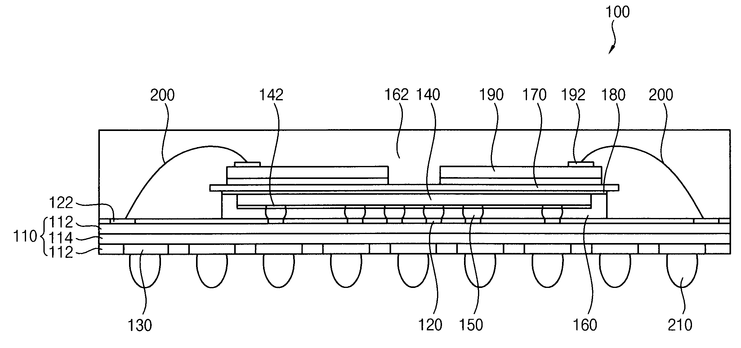
도 1은 본 발명의 일 실시예에 따른 반도체 패키지를 나타낸 단면도이다.
도 2 내지 도 6은 도 1에 도시된 반도체 패키지를 제조하는 방법을 순차적으로 나타낸 단면도들이다.
도 7은 본 발명의 다른 실시예에 따른 반도체 패키지를 나타낸 단면도이다.
도 8은 본 발명의 또 다른 실시예에 따른 반도체 패키지를 나타낸 단면도이다.
도 9는 본 발명의 또 다른 실시예에 따른 반도체 패키지를 나타낸 단면도이다.1 is a cross-sectional view illustrating a semiconductor package according to an embodiment of the present invention.
2 to 6 are cross-sectional views sequentially illustrating a method of manufacturing the semiconductor package illustrated in FIG. 1 .
7 is a cross-sectional view illustrating a semiconductor package according to another embodiment of the present invention.
8 is a cross-sectional view illustrating a semiconductor package according to another embodiment of the present invention.
9 is a cross-sectional view illustrating a semiconductor package according to another embodiment of the present invention.
이하, 첨부한 도면들을 참조하여 본 발명의 바람직한 실시예들을 상세히 설명한다.Hereinafter, preferred embodiments of the present invention will be described in detail with reference to the accompanying drawings.
도 1은 본 발명의 일 실시예에 따른 반도체 패키지를 나타낸 단면도이다.1 is a cross-sectional view illustrating a semiconductor package according to an embodiment of the present invention.
도 1을 참조하면, 본 실시예에 따른 반도체 패키지(100)는 패키지 기판(110), 적어도 하나의 로직 칩(140), 히트 싱크(170) 및 적어도 하나의 메모리 칩(190)을 포함할 수 있다. 이와 같이, 본 실시예의 반도체 패키지(100)는 로직 칩(140)과 메모리 칩(190)을 포함하는 시스템-인 패키지에 해당될 수 있다.Referring to FIG. 1 , the
패키지 기판(110)은 절연 기판(112), 도전층(114), 상부 패드들 및 하부 패드(130)들을 포함할 수 있다. 도전층(114)은 절연 기판(112)의 내부에 형성될 수 있다. 도전층(114)은 절연 기판(112)의 상부면과 하부면을 통해서 부분적으로 노출될 수 있다. 상부 패드들은 절연 기판(112)의 상부면을 통해 노출된 도전층(114) 부분들 상에 배치될 수 있다. 하부 패드(130)들은 절연 기판(112)의 하부면을 통해 노출된 도전층(114) 부분들 상에 배치될 수 있다. 외부접속단자(210)들이 하부 패드(130)들에 실장될 수 있다.The
상부 패드들은 제 1 신호 패드(120)들 및 제 2 신호 패드들(122)을 포함할 수 있다. 제 1 신호 패드(120)들은 절연 기판(112)의 상부면 중앙부에 배열될 수 있다. 제 1 신호 패드(120)들은 로직 칩(140)의 하부에 위치할 수 있다. 제 2 신호 패드(122)들은 절연 기판(112)의 상부면 가장자리에 배열될 수 있다. 제 2 신호 패드(122)들은 로직 칩(140)의 측면으로부터 노출될 수 있다. The upper pads may include
로직 칩(140)은 패키지 기판(110)의 중앙부 상부에 배치될 수 있다. 도전성 범프(150)들이 로직 칩(140)과 패키지 기판(110) 사이에 개재되어, 로직 칩(140)을 패키지 기판(110)에 전기적으로 연결시킬 수 있다. 구체적으로, 도전성 범프(150)들은 제 1 신호 패드(120)들 상에 배치될 수 있다. 로직 칩(140)의 하부면에 배열된 패드(142)들이 도전성 범프(150)들에 전기적으로 접촉될 수 있다. 따라서, 로직 칩(140)의 패드(142)들은 도전성 범프(150)들을 매개로 제 1 신호 패드(120)들에 전기적으로 연결될 수 있다.The
제 1 몰딩 부재(160)가 패키지 기판(110)의 상부면 중앙부에 형성되어 로직 칩(140)을 부분적으로 덮을 수 있다. 그러나, 로직 칩(140)의 상부면은 제 1 몰딩 부재(160)로 덮이지 않을 수 있다. 따라서, 로직 칩(140)의 상부면은 위를 향해 노출될 수 있다. 또한, 제 1 몰딩 부재(160)는 제 2 신호 패드(122)를 덮지 않을 수 있다. 따라서, 제 2 신호 패드(122)는 위를 향해 노출될 수 있다. 제 1 몰딩 부재(160)는 제 1 열전도율을 갖는 제 1 몰딩 물질을 포함할 수 있다.The
히트 싱크(170)는 로직 칩(140)과 제 1 몰딩 부재(160)의 상부면들에 배치될 수 있다. 특히, 히트 싱크(170)는 전열성 접착제(180)를 매개로 로직 칩(140)의 상부면에 부착될 수 있다. 전열성 접착제(180)는 로직 칩(140)의 상부면을 통해 방출된 열을 히트 싱크(170)로 전달할 수 있는 특성을 가질 수 있다. 예를 들어서, 전열성 접착제(180)는 서멀 인터페이스 물질(Thermal Interface Material : TIM)을 포함할 수 있다. 그러나, 히트 싱크(170)는 전열성 접착제(180)가 아닌 일반적인 접착제를 매개로 로직 칩(140)에 부착될 수도 있다.The
본 실시예에서, 히트 싱크(170)는 패키지 기판(110)과 전기적으로 절연될 수 있다. 즉, 히트 싱크(170)는 패키지 기판(110)에 연결되지 않을 수 있다. 히트 싱크(170)는 반도체 패키지(100)의 내부에 배치되어, 로직 칩(140)에서 발생된 열을 반도체 패키지(100)의 외부로 방출하는 기능만을 가질 수 있다. 히트 싱크(170)는 열을 외부로 신속하게 방출할 수 있는 금속 물질을 포함할 수 있다. 금속 물질의 종류는 특정 물질로 국한되지 않을 수 있다.In this embodiment, the
메모리 칩(190)은 히트 싱크(170)의 상부면에 배치될 수 있다. 본 실시예에서, 메모리 칩(190)은 히트 싱크(170)의 상부면 양측 가장자리들에 배치된 한 쌍으로 이루어질 수 있다. 패드(192)는 메모리 칩(190)들의 상부면에 배치될 수 있다.The
메모리 칩(190)의 패드(192)는 도전성 와이어(200)를 매개로 제 2 신호 패드(122)에 전기적으로 연결될 수 있다. 히트 싱크(170)는 패키지 기판(110)에 전기적으로 연결되어 있지 않으므로, 메모리 칩(190)은 히트 싱크(170)를 경유하지 않고 도전성 와이어(200)를 통해서 패키지 기판(110)에 직접 전기적으로 연결될 수 있다.The
제 2 몰딩 부재(162)가 패키지 기판(110)의 상부면에 형성되어, 히트 싱크(170), 메모리 칩(190) 및 도전성 와이어(200)를 덮을 수 있다. 제 2 몰딩 부재(162)는 제 2 열전도율을 갖는 제 2 몰딩 물질을 포함할 수 있다. 제 2 열전도율은 제 1 열전도율과 실질적으로 동일하거나 또는 상이할 수도 있다. 예를 들어서, 제 2 전도율은 제 1 전도율보다 높을 수 있다.The
본 실시예에 따르면, 메모리 칩(190)이 실장되는 기존의 패키지 기판이 히트 싱크(170)로 대체될 수 있다. 한편, 히트 싱크(170) 상에 배치된 메모리 칩(190)은 히트 싱크(170)를 경유하지 않고 도전성 와이어(200)를 통해서 패키지 기판(110)에 직접 전기적으로 연결될 수 있다. 이와 같이, 로직 칩(140)에 직접 접촉된 히트 싱크(170)가 반도체 패키지(100)의 내부에 배치됨으로써, 로직 칩(140)으로부터 발생된 열이 히트 싱크(170)와 제 2 몰딩 부재(162)를 통해서 신속하게 방출될 수 있다. According to the present embodiment, the existing package substrate on which the
도 2 내지 도 6은 도 1에 도시된 반도체 패키지를 제조하는 방법을 순차적으로 나타낸 단면도들이다.2 to 6 are cross-sectional views sequentially illustrating a method of manufacturing the semiconductor package illustrated in FIG. 1 .
도 2를 참조하면, 도전성 범프(150)들을 패키지 기판(110)의 제 1 신호 패드(120)들 상에 배치할 수 있다. 로직 칩(140)을 도전성 범프(150)들 상에 배치할 수 있다. 따라서, 로직 칩(140)의 패드(142)들은 도전성 범프(150)들을 매개로 제 1 신호 패드(120)들에 전기적으로 연결될 수 있다. 제 1 몰딩 부재(160)를 패키지 기판(110)의 상부면에 형성하여, 로직 칩(140)의 측면들을 제 1 몰딩 부재(160)로 둘러쌀 수 있다. 제 1 몰딩 부재(160)는 로직 칩(140)의 상부면에 형성되지 않을 수 있다. 따라서, 로직 칩(140)의 상부면은 위를 향해 노출될 수 있다.Referring to FIG. 2 ,
도 3을 참조하면, 히트 싱크(170)를 전열성 접착제(180), 즉 TIM을 이용해서 노출된 로직 칩(140)의 상부면에 부착할 수 있다. 따라서, 히트 싱크(170)는 전열성 접착제(180)를 매개로 로직 칩(140)의 상부면에 접촉될 수 있다. 그러므로, 로직 칩(140)의 상부면을 통해 방출된 열은 전열성 접착제(180)를 통해서 히트 싱크(170)로 전달될 수 있다.Referring to FIG. 3 , the
도 4를 참조하면, 메모리 칩(190)들을 히트 싱크(170)의 상부면에 배치할 수 있다. 메모리 칩(190)의 패드(192)들은 메모리 칩(190)의 상부면에 위치할 수 있다.Referring to FIG. 4 ,
도 5를 참조하면, 메모리 칩(190)들의 패드(192)들을 도전성 와이어(200)들을 이용해서 제 2 신호 패드(122)에 전기적으로 연결시킬 수 있다. 즉, 도전성 와이어(200)의 상단은 메모리 칩(190)의 패드(192)에 연결되고, 도전성 와이어(200)의 하단은 제 2 신호 패드(122)에 연결될 수 있다.Referring to FIG. 5 , the
도 6을 참조하면, 제 2 몰딩 부재(162)를 패키지 기판(110)의 상부면에 형성하여, 메모리 칩(190)과 히트 싱크(170) 및 도전성 와이어(200)들을 제 2 몰딩 부재(162)로 덮을 수 있다.Referring to FIG. 6 , the
외부접속단자(210)들을 하부 패드(130)들 상에 실장하여, 도 1에 도시된 반도체 패키지(100)를 완성할 수 있다.The
도 7은 본 발명의 다른 실시예에 따른 반도체 패키지를 나타낸 단면도이다.7 is a cross-sectional view illustrating a semiconductor package according to another embodiment of the present invention.
본 실시예에 따른 반도체 패키지(100a)는 패키지 기판과 히트 싱크를 제외하고는 도 1에 도시된 반도체 패키지(100)의 구성요소들과 실질적으로 동일한 구성요소들을 포함할 수 있다. 따라서, 동일한 구성요소들은 동일한 참조부호들로 나타내고, 또한 동일한 구성요소들에 대한 반복 설명은 생략할 수 있다.The
도 7을 참조하면, 패키지 기판(110a)은 제 1 더미 패드(124)와 제 2 더미 패드(126) 및 열 전달 라인(116)을 더 포함할 수 있다.Referring to FIG. 7 , the
제 1 더미 패드(124)는 절연 기판(112)의 상부면 중앙부에 배치될 수 있다. 제 1 더미 패드(124)는 도전층(114)에 연결되지 않을 수 있다. 즉, 제 1 더미 패드(124)는 도전층(114)과 전기적으로 절연될 수 있다. 특히, 제 1 더미 패드(124)는 로직 칩(140) 내의 회로에 전기적으로 연결되지 않을 수 있다. 따라서, 로직 칩(140) 내의 회로에서 발생된 신호는 제 1 더미 패드(124)로 전송되지 않을 수 있다.The
제 2 더미 패드(126)는 제 1 신호 패드(120)와 제 2 신호 패드(122) 사이인 절연 기판(112)의 상부면 부위에 배치될 수 있다. 제 2 더미 패드(126)는 도전층(114)에 연결되지 않을 수 있다. 즉, 제 2 더미 패드(126)는 도전층(114)과 전기적으로 절연될 수 있다. The
제 1 더미 패드(124)와 제 2 더미 패드(126)는 열 전달 라인(116)을 매개로 서로 연결될 수 있다. 열 전달 라인(116)은 절연 기판(112) 내에 형성될 수 있다. 열 전달 라인(116)은 도전층(114)에 연결되지 않을 수 있다. 열 전달 라인(116)은 로직 칩(140)의 하부면을 통해 방출되어 제 1 더미 패드(124)로 전달된 열을 제 2 더미 패드(126)로 전달할 수 있다. 본 실시예에서, 열 전달 라인(116)은 열을 제 1 더미 패드(124)로부터 제 2 더미 패드(126)로 신속하게 전달할 수 있는 금속 물질을 포함할 수 있다. 그러나, 열 전달 라인(116)은 금속 물질 이외에도 열 전달이 가능한 다른 물질들을 포함할 수도 있다.The
제 1 더미 범프(154)가 제 1 더미 패드(124) 상에 배치될 수 있다. 제 1 더미 범프(154)는 로직 칩(140)의 하부면에 접촉될 수 있다. 그러나, 제 1 더미 범프(154)는 로직 칩(140) 내의 회로에는 전기적으로 연결되지 않을 수 있다. 제 1 더미 범프(154)는 로직 칩(140)의 하부면을 통해 방출된 열을 제 1 더미 패드(124)와 열 전달 라인(116)을 통해서 제 2 더미 패드(126)로 전달할 수 있다.A
제 2 더미 범프(156)는 제 2 더미 패드(126) 상에 배치될 수 있다. 따라서, 로직 칩(140)의 하부면을 통해 방출된 열은 제 1 더미 범프(154), 제 1 더미 패드(124), 열 전달 라인(116) 및 제 2 더미 패드(126)를 통해서 제 2 더미 범프(156)로 전달될 수 있다. 제 1 및 제 2 더미 범프(154, 156)들은 도전성 범프(150)들과 함께 형성될 수 있다.The
히트 싱크(170a)는 열 전달부(172)를 포함할 수 있다. 열 전달부(172)는 히트 싱크(170a)의 측면으로부터 연장될 수 있다. 열 전달부(172)는 제 2 더미 범프(156)에 연결될 수 있다. 다른 실시예로서, 열 전달부(172)는 제 2 더미 패드(126)에 직접 연결될 수도 있다. 본 실시예에서, 열 전달부(172)는 패키지 기판(110a)의 중앙부를 향해 구부러진 형상을 가질 수 있다. 다른 실시예로서, 열 전달부(172)는 직선 형상을 가질 수도 있다.The heat sink 170a may include a
본 실시예에 따르면, 로직 칩(140)의 상부면을 통해 방출된 열은 히트 싱크(170a)로 전달될 수 있다. 또한, 로직 칩(140)의 하부면을 통해 방출된 열은 제 1 더미 범프(154), 제 1 더미 패드(124), 열 전달 라인(116), 제 2 더미 패드(126), 제 2 더미 범프(156) 및 열 전달부(172)를 통해서 히트 싱크(170a)로 전달될 수 있다. 이와 같이, 히트 싱크(170a)는 로직 칩(140)의 상부면을 통해 방출된 열뿐만 아니라 로직 칩(140)의 하부면을 통해 방출된 열도 신속하게 외부로 방출시킬 수 있다.According to the present embodiment, heat emitted through the upper surface of the
본 실시예의 반도체 패키지(100a)를 제조하는 방법은 히트 싱크(170a)를 로직 칩(140)의 상부면에 부착하는 공정이 열 전달부(172)를 제 2 더미 범프(156)에 연결시키는 공정을 더 포함한다는 점을 제외하고는 도 2 내지 도 6을 참조로 설명한 공정들과 실질적으로 동일한 공정들을 포함할 수 있다. 따라서, 본 실시예의 반도체 패키지(100a)를 제조하는 방법에 대한 반복 설명은 생략할 수 있다.In the method of manufacturing the
도 8은 본 발명의 또 다른 실시예에 따른 반도체 패키지를 나타낸 단면도이다.8 is a cross-sectional view illustrating a semiconductor package according to another embodiment of the present invention.
본 실시예에 따른 반도체 패키지(100b)는 열 전달부의 형상을 제외하고는 도 7에 도시된 반도체 패키지(100a)의 구성요소들과 실질적으로 동일한 구성요소들을 포함할 수 있다. 따라서, 동일한 구성요소들은 동일한 참조부호들로 나타내고, 또한 동일한 구성요소들에 대한 반복 설명은 생략할 수 있다.The
도 8을 참조하면, 히트 싱크(170b)는 열 전달부(174)를 포함할 수 있다. 열 전달부(174)는 패키지 기판(110a)의 가장자리를 향해 구부러진 형상을 가질 수 있다. 열 전달부(174)는 제 2 더미 범프(156)에 연결될 수 있다. 다른 실시예로서, 열 전달부(174)는 제 2 더미 패드(126)에 직접 연결될 수도 있다. 또한, 열 전달부(174)는 직선 형상을 가질 수도 있다.Referring to FIG. 8 , the
본 실시예의 반도체 패키지(100b)를 제조하는 방법은 히트 싱크(170a)를 로직 칩(140)의 상부면에 부착하는 공정이 열 전달부(174)를 제 2 더미 범프(156)에 연결시키는 공정을 더 포함한다는 점을 제외하고는 도 2 내지 도 6을 참조로 설명한 공정들과 실질적으로 동일한 공정들을 포함할 수 있다. 따라서, 본 실시예의 반도체 패키지(100b)를 제조하는 방법에 대한 반복 설명은 생략할 수 있다.In the method of manufacturing the
도 9는 본 발명의 또 다른 실시예에 따른 반도체 패키지를 나타낸 단면도이다.9 is a cross-sectional view illustrating a semiconductor package according to another embodiment of the present invention.
본 실시예에 따른 반도체 패키지(100c)는 외부 히트 싱크를 더 포함한다는 점을 제외하고는 도 1에 도시된 반도체 패키지(100)의 구성요소들과 실질적으로 동일한 구성요소들을 포함할 수 있다. 따라서, 동일한 구성요소들은 동일한 참조부호들로 나타내고, 또한 동일한 구성요소들에 대한 반복 설명은 생략할 수 있다.The
도 9를 참조하면, 제 2 몰딩 부재(162)는 히트 싱크(170)의 상부면을 노출시키는 개구부(164)를 가질 수 있다.Referring to FIG. 9 , the
외부 히트 싱크(220)는 제 2 몰딩 부재(162)의 외측면에 배치될 수 있다. 본 실시예에서, 외부 히트 싱크(220)는 제 2 몰딩 부재(162)의 상부면에 배치될 수 있다. 외부 히트 싱크(220)는 개구부(164) 내에 배치된 연결부(222)를 가질 수 있다. 연결부(222)는 개구부(164)를 완전히 매립할 수 있다. 다른 실시예로서, 연결부(222)는 개구부(164)를 부분적으로 매립할 수도 있다. 따라서, 외부 히트 싱크(220)는 연결부(222)를 매개로 히트 싱크(170)에 연결될 수 있다. 그러므로, 히트 싱크(170) 내의 열이 외부 히트 싱크(220)를 통해서 반도체 패키지(100c)의 외부로 신속하게 방출될 수 있다. 외부 히트 싱크(220)는 히트 싱크(170)의 재질과 동일한 재질을 포함할 수 있다. 그러나, 외부 히트 싱크(220)의 재질은 히트 싱크(170)의 재질과 상이할 수도 있다.The
반도체 패키지(100c)가 외부 히트 싱크(220)를 포함하는 경우, 로직 칩(140) 내의 열은 히트 싱크(170)와 외부 히트 싱크(220)를 통해서 신속하게 방출될 수 있다. 따라서, 제 2 몰딩 부재(162)는 높은 열전도율을 가질 필요가 없을 수 있다. 예를 들어서, 제 2 몰딩 부재(162)의 제 2 열전도율은 제 1 몰딩 부재(160)의 제 1 열전도율과 동일하거나 또는 제 1 열전도율보다 낮을 수 있다.When the
본 실시예의 외부 히트 싱크(220)는 도 7에 도시된 반도체 패키지(100a) 또는 도 8에 도시된 반도체 패키지(100b)에도 적용될 수 있다.The
또한, 본 실시예의 반도체 패키지(100c)를 제조하는 방법은 외부 히트 싱크(220)를 제 2 몰딩 부재(162)의 상부면에 배치하는 공정을 더 포함한다는 점을 제외하고는 도 2 내지 도 6을 참조로 설명한 공정들과 실질적으로 동일한 공정들을 포함할 수 있다. 따라서, 본 실시예의 반도체 패키지(100c)를 제조하는 방법에 대한 반복 설명은 생략할 수 있다.In addition, the method of manufacturing the
상기된 본 실시예들에 따르면, 메모리 칩이 실장되는 기존의 패키지 기판이 히트 싱크로 대체되면서 메모리 칩은 패키지 기판에 직접 연결됨으로써, 로직 칩으로부터 발생된 열이 히트 싱크를 통해서 신속하게 방출될 수 있다. 따라서, 반도체 패키지의 성능이 로직 칩으로부터 발생된 열에 의해 열화되는 것이 억제될 수 있다.According to the present exemplary embodiments, the memory chip is directly connected to the package substrate while the existing package substrate on which the memory chip is mounted is replaced with the heat sink, so that heat generated from the logic chip can be rapidly dissipated through the heat sink. . Accordingly, it can be suppressed that the performance of the semiconductor package is deteriorated by heat generated from the logic chip.
상술한 바와 같이, 본 발명의 바람직한 실시예들을 참조하여 설명하였지만 해당 기술 분야의 숙련된 당업자라면 하기의 특허 청구의 범위에 기재된 본 발명의 사상으로부터 벗어나지 않는 범위 내에서 본 발명을 다양하게 수정 및 변경시킬 수 있음을 이해할 수 있을 것이다.As described above, although described with reference to preferred embodiments of the present invention, those skilled in the art can variously modify and change the present invention without departing from the spirit of the present invention as set forth in the claims below. You will understand that it can be done.
110 ; 패키지 기판 112 ; 절연 기판
114 ; 도전층 116 ; 열 전달 라인
120 ; 제 1 신호 패드 122 ; 제 2 신호 패드
124 ; 제 1 더미 패드 126 ; 제 2 더미 패드
130 ; 하부 패드 140 ; 로직 칩
150 ; 도전성 범프 154 ; 제 1 더미 범프
156 ; 제 2 더미 범프 160 ; 제 1 몰딩 부재
162 ; 제 2 몰딩 부재 170 ; 히트 싱크
172, 174 ; 열 전달부 180 ; 전열성 접착제
190 ; 메모리 칩 200 ; 도전성 와이어
210 ; 외부접속단자 220 ; 외부 히트 싱크110 ;
114;
120 ;
124 ;
130 ;
150 ;
156;
162; a
172, 174;
190 ;
210;
Claims (10)
상기 패키지 기판의 상부면에 배치되어, 상기 패키지 기판에 전기적으로 연결된 로직 칩;
상기 로직 칩의 상부면과 접촉되어, 상기 로직 칩에서 발생된 열을 방출시키는 히트 싱크(heat sink);
상기 히트 싱크의 상부면에 배치되고, 상기 패키지 기판에 전기적으로 연결된 2개의 메모리 칩들;
상기 로직 칩의 상부면이 노출되도록 상기 로직 칩의 측면들을 둘러싸는 제 1 몰딩 부재;
상기 2개의 메모리 칩을 덮고, 상기 2개의 메모리 칩들 사이에 위치한 상기 히트 싱크의 상부면을 노출시키는 개구부를 갖는 제 2 몰딩 부재; 및
상기 제 2 몰딩 부재의 상부면에 배치되고, 상기 개구부를 매립하여 상기 히트 싱크의 노출된 상부면에 연결된 연결부를 갖는 외부 히트 싱크를 포함하는 반도체 패키지.package substrate;
a logic chip disposed on an upper surface of the package substrate and electrically connected to the package substrate;
a heat sink in contact with an upper surface of the logic chip to dissipate heat generated by the logic chip;
two memory chips disposed on an upper surface of the heat sink and electrically connected to the package substrate;
a first molding member surrounding side surfaces of the logic chip to expose an upper surface of the logic chip;
a second molding member covering the two memory chips and having an opening exposing an upper surface of the heat sink positioned between the two memory chips; and
and an external heat sink disposed on an upper surface of the second molding member and having a connection portion connected to the exposed upper surface of the heat sink by filling the opening.
절연 기판;
상기 절연 기판 내에 형성된 도전층;
상기 절연 기판의 상부면에 배치되어, 상기 로직 칩을 상기 도전층에 전기적으로 연결시키는 제 1 신호 패드; 및
상기 절연 기판의 상부면에 배치되어, 상기 메모리 칩을 상기 도전층에 전기적으로 연결시키는 제 2 신호 패드를 포함하는 반도체 패키지.The method of claim 1 , wherein the package substrate comprises:
insulated substrate;
a conductive layer formed in the insulating substrate;
a first signal pad disposed on the upper surface of the insulating substrate and electrically connecting the logic chip to the conductive layer; and
and a second signal pad disposed on an upper surface of the insulating substrate to electrically connect the memory chip to the conductive layer.
상기 절연 기판의 상부면에 배치되어, 상기 로직 칩에 접촉된 제 1 더미 패드;
상기 절연 기판의 상부면에 배치되어, 상기 히트 싱크에 연결된 제 2 더미 패드; 및
상기 제 1 더미 패드와 상기 제 2 더미 패드를 연결하여, 상기 제 1 더미 패드로부터 상기 제 2 더미 패드로 이어지는 상기 열의 전달 경로를 형성하는 열 전달 라인을 더 포함하는 반도체 패키지.The method of claim 5, wherein the package substrate is
a first dummy pad disposed on the upper surface of the insulating substrate and in contact with the logic chip;
a second dummy pad disposed on the upper surface of the insulating substrate and connected to the heat sink; and
and a heat transfer line connecting the first dummy pad and the second dummy pad to form a heat transfer path from the first dummy pad to the second dummy pad.
The semiconductor package of claim 1 , wherein the heat sink is attached to the upper surface of the logic chip through a thermal interface material (TIM).
Priority Applications (4)
| Application Number | Priority Date | Filing Date | Title |
|---|---|---|---|
| KR1020190113334A KR102359904B1 (en) | 2019-09-16 | 2019-09-16 | Semiconductor package |
| US16/814,336 US11257784B2 (en) | 2019-09-16 | 2020-03-10 | Semiconductor package |
| US17/588,442 US11996387B2 (en) | 2019-09-16 | 2022-01-31 | Semiconductor package |
| US18/651,786 US20240290751A1 (en) | 2019-09-16 | 2024-05-01 | Semiconductor package |
Applications Claiming Priority (1)
| Application Number | Priority Date | Filing Date | Title |
|---|---|---|---|
| KR1020190113334A KR102359904B1 (en) | 2019-09-16 | 2019-09-16 | Semiconductor package |
Publications (2)
| Publication Number | Publication Date |
|---|---|
| KR20210032081A KR20210032081A (en) | 2021-03-24 |
| KR102359904B1 true KR102359904B1 (en) | 2022-02-08 |
Family
ID=74868664
Family Applications (1)
| Application Number | Title | Priority Date | Filing Date |
|---|---|---|---|
| KR1020190113334A Active KR102359904B1 (en) | 2019-09-16 | 2019-09-16 | Semiconductor package |
Country Status (2)
| Country | Link |
|---|---|
| US (3) | US11257784B2 (en) |
| KR (1) | KR102359904B1 (en) |
Families Citing this family (3)
| Publication number | Priority date | Publication date | Assignee | Title |
|---|---|---|---|---|
| KR102359904B1 (en) * | 2019-09-16 | 2022-02-08 | 삼성전자주식회사 | Semiconductor package |
| KR102746861B1 (en) * | 2020-04-24 | 2024-12-27 | 삼성전자주식회사 | Semiconductor package |
| KR20240023263A (en) * | 2022-08-11 | 2024-02-21 | 삼성전자주식회사 | Semiconductor package |
Citations (3)
| Publication number | Priority date | Publication date | Assignee | Title |
|---|---|---|---|---|
| JP2000269411A (en) * | 1999-03-17 | 2000-09-29 | Shinko Electric Ind Co Ltd | Semiconductor device and manufacturing method thereof |
| JP2007234683A (en) * | 2006-02-28 | 2007-09-13 | Matsushita Electric Ind Co Ltd | Semiconductor device and manufacturing method thereof |
| US20190043722A1 (en) * | 2017-08-03 | 2019-02-07 | Tokyo Electron Limited | Substrate treatment method, computer storage medium and substrate treatment system |
Family Cites Families (20)
| Publication number | Priority date | Publication date | Assignee | Title |
|---|---|---|---|---|
| JP3198796B2 (en) | 1993-06-25 | 2001-08-13 | 富士電機株式会社 | Mold module |
| JP3982876B2 (en) * | 1997-06-30 | 2007-09-26 | 沖電気工業株式会社 | Surface acoustic wave device |
| US6197614B1 (en) | 1999-12-20 | 2001-03-06 | Thin Film Module, Inc. | Quick turn around fabrication process for packaging substrates and high density cards |
| KR100649869B1 (en) * | 2000-12-04 | 2006-11-24 | 앰코 테크놀로지 코리아 주식회사 | Semiconductor package |
| TW517361B (en) | 2001-12-31 | 2003-01-11 | Megic Corp | Chip package structure and its manufacture process |
| US6869825B2 (en) | 2002-12-31 | 2005-03-22 | Intel Corporation | Folded BGA package design with shortened communication paths and more electrical routing flexibility |
| KR100630690B1 (en) * | 2004-07-08 | 2006-10-02 | 삼성전자주식회사 | Multichip Package with Heat Dissipation Path |
| US7786591B2 (en) | 2004-09-29 | 2010-08-31 | Broadcom Corporation | Die down ball grid array package |
| US7429786B2 (en) | 2005-04-29 | 2008-09-30 | Stats Chippac Ltd. | Semiconductor package including second substrate and having exposed substrate surfaces on upper and lower sides |
| KR100782798B1 (en) | 2006-02-22 | 2007-12-05 | 삼성전기주식회사 | Substrate Package and Manufacturing Method Thereof |
| US7696618B2 (en) | 2007-11-21 | 2010-04-13 | Powertech Technology Inc. | POP (package-on-package) semiconductor device |
| US8841765B2 (en) * | 2011-04-22 | 2014-09-23 | Tessera, Inc. | Multi-chip module with stacked face-down connected dies |
| KR20130102405A (en) * | 2012-03-07 | 2013-09-17 | 삼성전자주식회사 | Flip chip package and method of manufacturing the same |
| KR102127772B1 (en) * | 2013-05-16 | 2020-06-29 | 삼성전자주식회사 | Semiconductor package having heat spreader and method of forming the same |
| KR102372300B1 (en) | 2015-11-26 | 2022-03-08 | 삼성전자주식회사 | Stacked package and method of manufacturing the same |
| US10607909B2 (en) * | 2016-04-02 | 2020-03-31 | Intel Corporation | Systems, methods, and apparatuses for implementing a thermal solution for 3D packaging |
| KR102397902B1 (en) * | 2018-01-29 | 2022-05-13 | 삼성전자주식회사 | Semiconductor package |
| KR102609445B1 (en) * | 2018-10-22 | 2023-12-04 | 삼성전자주식회사 | Semiconductor package |
| KR20200144370A (en) * | 2019-06-18 | 2020-12-29 | 삼성전자주식회사 | Semiconductor packages having heat spreader |
| KR102359904B1 (en) * | 2019-09-16 | 2022-02-08 | 삼성전자주식회사 | Semiconductor package |
-
2019
- 2019-09-16 KR KR1020190113334A patent/KR102359904B1/en active Active
-
2020
- 2020-03-10 US US16/814,336 patent/US11257784B2/en active Active
-
2022
- 2022-01-31 US US17/588,442 patent/US11996387B2/en active Active
-
2024
- 2024-05-01 US US18/651,786 patent/US20240290751A1/en active Pending
Patent Citations (3)
| Publication number | Priority date | Publication date | Assignee | Title |
|---|---|---|---|---|
| JP2000269411A (en) * | 1999-03-17 | 2000-09-29 | Shinko Electric Ind Co Ltd | Semiconductor device and manufacturing method thereof |
| JP2007234683A (en) * | 2006-02-28 | 2007-09-13 | Matsushita Electric Ind Co Ltd | Semiconductor device and manufacturing method thereof |
| US20190043722A1 (en) * | 2017-08-03 | 2019-02-07 | Tokyo Electron Limited | Substrate treatment method, computer storage medium and substrate treatment system |
Also Published As
| Publication number | Publication date |
|---|---|
| US20220157776A1 (en) | 2022-05-19 |
| KR20210032081A (en) | 2021-03-24 |
| US11996387B2 (en) | 2024-05-28 |
| US20240290751A1 (en) | 2024-08-29 |
| US11257784B2 (en) | 2022-02-22 |
| US20210082872A1 (en) | 2021-03-18 |
Similar Documents
| Publication | Publication Date | Title |
|---|---|---|
| KR102609445B1 (en) | Semiconductor package | |
| JP5149178B2 (en) | Packaged integrated circuits with enhanced heat dissipation | |
| US8564124B2 (en) | Semiconductor package | |
| US6650006B2 (en) | Semiconductor package with stacked chips | |
| US6566164B1 (en) | Exposed copper strap in a semiconductor package | |
| JPH11312764A (en) | Area array type semiconductor package and manufacturing method thereof | |
| US20240290751A1 (en) | Semiconductor package | |
| JPH0923076A (en) | Integrated circuit package consisting of multiple heat transfer paths for enhanced heat dissipation and a cap around the edges for improved package integrity and reliability | |
| JP2008091714A (en) | Semiconductor device | |
| JP2000068403A (en) | Semiconductor device and substrate connection structure thereof | |
| CN218957731U (en) | packaging for integrated circuits | |
| US20210202352A1 (en) | Semiconductor package for discharging heat generated by semiconductor chip | |
| TW201916279A (en) | Chip package | |
| KR100598652B1 (en) | Semiconductor device | |
| JP2018190882A (en) | Semiconductor device | |
| KR20030045950A (en) | Multi chip package comprising heat sinks | |
| US6847111B2 (en) | Semiconductor device with heat-dissipating capability | |
| KR102016019B1 (en) | High thermal conductivity semiconductor package | |
| US20060145312A1 (en) | Dual flat non-leaded semiconductor package | |
| CN110957277B (en) | Inverter power system and manufacturing method thereof | |
| JP4225243B2 (en) | Semiconductor device and substrate connection structure | |
| JP4371946B2 (en) | Semiconductor device and substrate connection structure thereof | |
| TWI220783B (en) | A semiconductor device having a heat-dissipating structure | |
| KR101473356B1 (en) | Grounding method of heat-slug | |
| JP2010141175A (en) | Semiconductor device |
Legal Events
| Date | Code | Title | Description |
|---|---|---|---|
| PA0109 | Patent application |
St.27 status event code: A-0-1-A10-A12-nap-PA0109 |
|
| PA0201 | Request for examination |
St.27 status event code: A-1-2-D10-D11-exm-PA0201 |
|
| D13-X000 | Search requested |
St.27 status event code: A-1-2-D10-D13-srh-X000 |
|
| D14-X000 | Search report completed |
St.27 status event code: A-1-2-D10-D14-srh-X000 |
|
| PE0902 | Notice of grounds for rejection |
St.27 status event code: A-1-2-D10-D21-exm-PE0902 |
|
| P11-X000 | Amendment of application requested |
St.27 status event code: A-2-2-P10-P11-nap-X000 |
|
| P13-X000 | Application amended |
St.27 status event code: A-2-2-P10-P13-nap-X000 |
|
| PG1501 | Laying open of application |
St.27 status event code: A-1-1-Q10-Q12-nap-PG1501 |
|
| E90F | Notification of reason for final refusal | ||
| PE0902 | Notice of grounds for rejection |
St.27 status event code: A-1-2-D10-D21-exm-PE0902 |
|
| P11-X000 | Amendment of application requested |
St.27 status event code: A-2-2-P10-P11-nap-X000 |
|
| P13-X000 | Application amended |
St.27 status event code: A-2-2-P10-P13-nap-X000 |
|
| E701 | Decision to grant or registration of patent right | ||
| PE0701 | Decision of registration |
St.27 status event code: A-1-2-D10-D22-exm-PE0701 |
|
| GRNT | Written decision to grant | ||
| PR0701 | Registration of establishment |
St.27 status event code: A-2-4-F10-F11-exm-PR0701 |
|
| PR1002 | Payment of registration fee |
St.27 status event code: A-2-2-U10-U11-oth-PR1002 Fee payment year number: 1 |
|
| PG1601 | Publication of registration |
St.27 status event code: A-4-4-Q10-Q13-nap-PG1601 |
|
| PR1001 | Payment of annual fee |
St.27 status event code: A-4-4-U10-U11-oth-PR1001 Fee payment year number: 4 |
|
| P22-X000 | Classification modified |
St.27 status event code: A-4-4-P10-P22-nap-X000 |
|
| PR1001 | Payment of annual fee |
St.27 status event code: A-4-4-U10-U11-oth-PR1001 Fee payment year number: 5 |