KR102353261B1 - Overlay metrology systems and methods - Google Patents
Overlay metrology systems and methods Download PDFInfo
- Publication number
- KR102353261B1 KR102353261B1 KR1020207032205A KR20207032205A KR102353261B1 KR 102353261 B1 KR102353261 B1 KR 102353261B1 KR 1020207032205 A KR1020207032205 A KR 1020207032205A KR 20207032205 A KR20207032205 A KR 20207032205A KR 102353261 B1 KR102353261 B1 KR 102353261B1
- Authority
- KR
- South Korea
- Prior art keywords
- illumination
- sample
- signals
- metrology system
- overlay error
- Prior art date
- Legal status (The legal status is an assumption and is not a legal conclusion. Google has not performed a legal analysis and makes no representation as to the accuracy of the status listed.)
- Active
Links
Images


Classifications
-
- H—ELECTRICITY
- H01—ELECTRIC ELEMENTS
- H01L—SEMICONDUCTOR DEVICES NOT COVERED BY CLASS H10
- H01L22/00—Testing or measuring during manufacture or treatment; Reliability measurements, i.e. testing of parts without further processing to modify the parts as such; Structural arrangements therefor
- H01L22/10—Measuring as part of the manufacturing process
- H01L22/12—Measuring as part of the manufacturing process for structural parameters, e.g. thickness, line width, refractive index, temperature, warp, bond strength, defects, optical inspection, electrical measurement of structural dimensions, metallurgic measurement of diffusions
-
- G—PHYSICS
- G01—MEASURING; TESTING
- G01B—MEASURING LENGTH, THICKNESS OR SIMILAR LINEAR DIMENSIONS; MEASURING ANGLES; MEASURING AREAS; MEASURING IRREGULARITIES OF SURFACES OR CONTOURS
- G01B11/00—Measuring arrangements characterised by the use of optical techniques
- G01B11/26—Measuring arrangements characterised by the use of optical techniques for measuring angles or tapers; for testing the alignment of axes
- G01B11/27—Measuring arrangements characterised by the use of optical techniques for measuring angles or tapers; for testing the alignment of axes for testing the alignment of axes
- G01B11/272—Measuring arrangements characterised by the use of optical techniques for measuring angles or tapers; for testing the alignment of axes for testing the alignment of axes using photoelectric detection means
-
- G—PHYSICS
- G03—PHOTOGRAPHY; CINEMATOGRAPHY; ANALOGOUS TECHNIQUES USING WAVES OTHER THAN OPTICAL WAVES; ELECTROGRAPHY; HOLOGRAPHY
- G03F—PHOTOMECHANICAL PRODUCTION OF TEXTURED OR PATTERNED SURFACES, e.g. FOR PRINTING, FOR PROCESSING OF SEMICONDUCTOR DEVICES; MATERIALS THEREFOR; ORIGINALS THEREFOR; APPARATUS SPECIALLY ADAPTED THEREFOR
- G03F7/00—Photomechanical, e.g. photolithographic, production of textured or patterned surfaces, e.g. printing surfaces; Materials therefor, e.g. comprising photoresists; Apparatus specially adapted therefor
- G03F7/70—Microphotolithographic exposure; Apparatus therefor
- G03F7/70483—Information management; Active and passive control; Testing; Wafer monitoring, e.g. pattern monitoring
- G03F7/70605—Workpiece metrology
- G03F7/70616—Monitoring the printed patterns
- G03F7/70633—Overlay, i.e. relative alignment between patterns printed by separate exposures in different layers, or in the same layer in multiple exposures or stitching
-
- G—PHYSICS
- G01—MEASURING; TESTING
- G01N—INVESTIGATING OR ANALYSING MATERIALS BY DETERMINING THEIR CHEMICAL OR PHYSICAL PROPERTIES
- G01N21/00—Investigating or analysing materials by the use of optical means, i.e. using sub-millimetre waves, infrared, visible or ultraviolet light
- G01N21/84—Systems specially adapted for particular applications
- G01N21/88—Investigating the presence of flaws or contamination
- G01N21/95—Investigating the presence of flaws or contamination characterised by the material or shape of the object to be examined
- G01N21/9501—Semiconductor wafers
-
- G—PHYSICS
- G03—PHOTOGRAPHY; CINEMATOGRAPHY; ANALOGOUS TECHNIQUES USING WAVES OTHER THAN OPTICAL WAVES; ELECTROGRAPHY; HOLOGRAPHY
- G03F—PHOTOMECHANICAL PRODUCTION OF TEXTURED OR PATTERNED SURFACES, e.g. FOR PRINTING, FOR PROCESSING OF SEMICONDUCTOR DEVICES; MATERIALS THEREFOR; ORIGINALS THEREFOR; APPARATUS SPECIALLY ADAPTED THEREFOR
- G03F7/00—Photomechanical, e.g. photolithographic, production of textured or patterned surfaces, e.g. printing surfaces; Materials therefor, e.g. comprising photoresists; Apparatus specially adapted therefor
- G03F7/70—Microphotolithographic exposure; Apparatus therefor
- G03F7/70483—Information management; Active and passive control; Testing; Wafer monitoring, e.g. pattern monitoring
- G03F7/70605—Workpiece metrology
- G03F7/70616—Monitoring the printed patterns
- G03F7/70625—Dimensions, e.g. line width, critical dimension [CD], profile, sidewall angle or edge roughness
-
- H—ELECTRICITY
- H01—ELECTRIC ELEMENTS
- H01L—SEMICONDUCTOR DEVICES NOT COVERED BY CLASS H10
- H01L22/00—Testing or measuring during manufacture or treatment; Reliability measurements, i.e. testing of parts without further processing to modify the parts as such; Structural arrangements therefor
- H01L22/20—Sequence of activities consisting of a plurality of measurements, corrections, marking or sorting steps
- H01L22/24—Optical enhancement of defects or not directly visible states, e.g. selective electrolytic deposition, bubbles in liquids, light emission, colour change
-
- H10P74/203—
-
- H10P74/235—
-
- G—PHYSICS
- G01—MEASURING; TESTING
- G01B—MEASURING LENGTH, THICKNESS OR SIMILAR LINEAR DIMENSIONS; MEASURING ANGLES; MEASURING AREAS; MEASURING IRREGULARITIES OF SURFACES OR CONTOURS
- G01B2210/00—Aspects not specifically covered by any group under G01B, e.g. of wheel alignment, caliper-like sensors
- G01B2210/56—Measuring geometric parameters of semiconductor structures, e.g. profile, critical dimensions or trench depth
Landscapes
- Physics & Mathematics (AREA)
- General Physics & Mathematics (AREA)
- Health & Medical Sciences (AREA)
- Life Sciences & Earth Sciences (AREA)
- Chemical & Material Sciences (AREA)
- Analytical Chemistry (AREA)
- Biochemistry (AREA)
- General Health & Medical Sciences (AREA)
- Immunology (AREA)
- Pathology (AREA)
- Length Measuring Devices By Optical Means (AREA)
- Testing Or Measuring Of Semiconductors Or The Like (AREA)
- Engineering & Computer Science (AREA)
- Investigating Materials By The Use Of Optical Means Adapted For Particular Applications (AREA)
- Investigating Or Analysing Materials By Optical Means (AREA)
- Manufacturing & Machinery (AREA)
- Computer Hardware Design (AREA)
- Microelectronics & Electronic Packaging (AREA)
- Power Engineering (AREA)
- Radar Systems Or Details Thereof (AREA)
Abstract
샘플의 오버레이 에러를 측정하기 위한 시스템이 개시된다. 이 시스템은 광대역 조명을 방출하도록 구성된 광대역 조명 광원을 포함할 수 있다. 이 시스템은 광대역 조명을 샘플 상에 배치된 타깃으로 지향시키도록 구성된 하나 이상의 광학 요소를 또한 포함할 수 있으며, 여기서 하나 이상의 광학 요소는 타깃으로부터의 조명을 수집하고 이를 분광계로 지향시키도록 구성되고, 여기서 분광계는 샘플로부터 수집된 조명의 다수의 파장을 센서의 다수의 요소로 분산시켜 복수의 신호를 생성하도록 구성된다. 이 시스템은 복수의 신호를 복수의 계산된 신호와 비교함으로써 타깃의 제1 구조체와 제2 구조체 사이의 오버레이 에러를 계산하도록 구성된 제어기를 또한 포함할 수 있다.A system for measuring overlay error of a sample is disclosed. The system may include a broadband illumination source configured to emit broadband illumination. The system may also include one or more optical elements configured to direct broadband illumination to a target disposed on the sample, wherein the one or more optical elements are configured to collect illumination from the target and direct it to the spectrometer; wherein the spectrometer is configured to disperse multiple wavelengths of illumination collected from the sample to multiple elements of the sensor to generate a plurality of signals. The system may also include a controller configured to calculate an overlay error between the first structure and the second structure of the target by comparing the plurality of signals to the plurality of calculated signals.
Description
관련 출원의 교차 참조Cross-reference to related applications
본 출원은 Yung-Ho Alex Chuang, Yinying Xiao-Li, John Fielden, Xuefeng Liu, 및 Peilin Jiang이 발명자로서 기명된, 발명의 명칭이 “OVERLAY METROLOGY SYSTEM AND METHOD”인, 2018년 3월 13일자로 출원된 미국 가출원 제62/642,501호의 35 U.S.C. § 119(e)에 따른 이익을 주장하며, 이 미국 가출원은 참조에 의해 전체가 본 명세서에 포함된다.This application was filed on March 13, 2018, entitled “OVERLAY METROLOGY SYSTEM AND METHOD”, named as inventors by Yung-Ho Alex Chuang, Yinying Xiao-Li, John Fielden, Xuefeng Liu, and Peilin Jiang 35 USC of U.S. Provisional Application No. 62/642,501 Claiming the benefit under § 119(e), this US provisional application is hereby incorporated by reference in its entirety.
기술 분야technical field
본 출원은 일반적으로 오버레이 계측에 관한 것이며, 특히 오버레이 계측 시스템에서 사용하기에 적합한 반도체 웨이퍼 스택의 단일 층 또는 다수의 층에 형성되는 구조체들 사이의 오버레이의 결정에 관한 것이다.BACKGROUND This application relates generally to overlay metrology, and more particularly to the determination of overlays between structures formed in a single layer or multiple layers of a semiconductor wafer stack suitable for use in an overlay metrology system.
집적 회로(IC) 산업은 점점 더 작은 결함 및 파티클을 검출하기 위해 점점 더 높은 민감도를 가진 검사 툴을 필요로 하고, 반도체 웨이퍼 상의 작은 피처의 치수를 정확하게 측정하기 위한 고정밀 계측 툴을 필요로 한다. 반도체 산업은 현재 대략 20 nm 이하의 피처 치수를 가진 반도체 디바이스를 제조하고 있다. 몇 년 내에, 이 산업은 대략 5 nm의 피처 치수를 가진 디바이스를 제조할 것이다. 크기가 몇 나노미터에 불과한 파티클 및 결함은 웨이퍼 수율을 감소시킬 수 있는 반면, 십분의 몇 나노미터 이하의 피처 치수 및 정렬의 변화는 트랜지스터 또는 메모리 디바이스의 전기적 성능의 상당한 변화 또는 고장을 야기할 수 있다.The integrated circuit (IC) industry requires inspection tools with increasingly high sensitivity to detect increasingly smaller defects and particles, and high precision metrology tools to accurately measure the dimensions of small features on semiconductor wafers. The semiconductor industry currently manufactures semiconductor devices with feature dimensions of approximately 20 nm or less. In a few years, the industry will manufacture devices with feature dimensions on the order of 5 nm. Particles and defects that are only a few nanometers in size can reduce wafer yield, whereas changes in feature dimensions and alignment of tenths of a nanometer or less can cause significant changes or failures in the electrical performance of a transistor or memory device. have.
반도체 계측 분야에서, 계측 툴은 타깃을 조명하는 조명 시스템, 타깃, 디바이스 또는 피처와 조명 시스템의 상호작용(또는 그의 결여)에 의해 제공되는 관련 정보를 캡처하는 수집 시스템, 및 수집된 정보를 하나 이상의 알고리즘을 사용하여 분석하는 프로세싱 시스템을 포함할 수 있다. 웨이퍼 상의 패터닝된 구조체의 폭, 웨이퍼 상에 형성된 막의 두께, 및 웨이퍼의 다른 층 상의 패터닝된 구조체에 대한 웨이퍼의 하나의 층 상의 패터닝된 구조체의 오버레이와 같은 웨이퍼의 다양한 특성을 측정하기 위해 반도체 제조 프로세스의 다양한 지점에서 웨이퍼에 대해 계측 프로세스가 수행된다. 이러한 측정은 반도체 다이의 제조에서의 프로세스 제어 및/또는 수율 효율을 용이하게 하기 위해 사용된다. 광학 임계 치수(CD) 계측은 현재 분광 산란측정법 또는 각도 분해 산란측정법을 사용하여 수행된다. 막 계측은 분광 엘립소메트리를 사용하여 수행된다. 광학 오버레이 계측은 이미징 방법 또는 산란측정법 기반 방법(분광 및 각도 분해 둘 모두) 중 어느 하나를 사용하여 수행된다. 반도체 및 관련 산업을 위한 오버레이 계측 툴은 KLA-Tencor Corporation(예를 들어, Archer 500 LCM), ASML Holding N.V.(예를 들어, YieldStar S-250D), 및 다른 회사에 의해 제조된다.In the field of semiconductor metrology, metrology tools include an illumination system that illuminates a target, a collection system that captures relevant information provided by the interaction (or lack thereof) of the illumination system with the target, device, or feature, and a collection system that captures the collected information in one or more It may include a processing system that analyzes using an algorithm. A semiconductor manufacturing process to measure various properties of a wafer, such as the width of the patterned structures on the wafer, the thickness of films formed on the wafer, and the overlay of the patterned structures on one layer of the wafer to the patterned structures on the other layers of the wafer. A metrology process is performed on the wafer at various points in Such measurements are used to facilitate process control and/or yield efficiencies in the fabrication of semiconductor dies. Optical critical dimension (CD) metrology is currently performed using either spectral scatterometry or angle resolved scatterometry. Membrane metrology is performed using spectroscopic ellipsometry. Optical overlay metrology is performed using either imaging methods or scatterometry based methods (both spectroscopic and angular resolution). Overlay metrology tools for semiconductor and related industries are manufactured by KLA-Tencor Corporation (eg, Archer 500 LCM), ASML Holding N.V. (eg, YieldStar S-250D), and others.
다양한 제조 및 생산 환경에서, 샘플의 다양한 층들 사이의 또는 이러한 샘플의 특정 층 내에서의 정렬을 제어할 필요가 있다. 예를 들어, 반도체 제조 산업에서, 전자 디바이스는 기판 상에 일련의 층들 - 이 층들 중 일부 또는 전부는 다양한 구조체를 포함함 - 을 제조함으로써 생산될 수 있다. 특정 층 내에서의 그러한 구조체의 상대 위치는 물론 다른 층에 있는 구조체에 대한 그러한 구조체의 상대 위치도 완성된 전자 디바이스의 성능과 관련성이 있거나 심지어 그에 크리티컬(critical)하다. 그러한 샘플 내에서의 구조체의 상대 위치는 오버레이라고 불린다.In various manufacturing and production environments, there is a need to control alignment between various layers of a sample or within a particular layer of such a sample. For example, in the semiconductor manufacturing industry, electronic devices can be produced by fabricating a series of layers, some or all of which include various structures, on a substrate. The relative position of such structures within a particular layer, as well as the relative position of such structures with respect to structures in other layers, is relevant or even critical to the performance of the finished electronic device. The relative position of a structure within such a sample is called an overlay.
웨이퍼 상의 연속적인 패터닝된 층들 사이의 오버레이 에러의 측정은 집적 회로 및 디바이스의 제조 프로세스에서 사용되는 가장 크리티컬한 프로세스 제어 기법들 중 하나이다. 오버레이 정확도는 일반적으로 제1 패터닝된 층이 그 위에 또는 그 아래에 배치된 제2 패터닝된 층에 대해 얼마나 정확하게 정렬되는지의 결정 및 제1 패턴이 동일한 층에 배치된 제2 패턴에 대해 얼마나 정확하게 정렬되는지의 결정에 관련된다.Measurement of overlay error between successive patterned layers on a wafer is one of the most critical process control techniques used in the manufacturing process of integrated circuits and devices. Overlay accuracy generally determines how accurately a first patterned layer aligns with respect to a second patterned layer disposed on or below it and how accurately a first pattern aligns with a second pattern disposed on the same layer. related to the decision to be
ITRS(International Technology Roadmap for Semiconductors)에 따르면 반도체 디바이스가 제대로 작동하기 위해서는 오버레이 에러가 패턴에서의 가장 작은 치수의 대략 20% 이내여야 한다. 오버레이 데이터에 요구되는 TMU(total measurement uncertainty)는 프로세스 공차보다 훨씬 더 작다. TMU에 대한 여러 원인(contributor)이 있다. 동일한 오버레이 계측 툴에서 웨이퍼가 180° 회전되어 재측정될 때 발생하는 오버레이 측정치의 차이인 TIS(tool-induced shift) 및 정밀도 면에서 측정 일관성이 평가된다. TMU에 대한 다른 원인은 측정된 데이터와 패터닝 툴 모델들에 대한 최적합(best fit) 사이의 변동, 오버레이 계측 툴들 사이의 측정치의 불일치, 및 동일한 인접 타깃들로부터의 결과의 차이를 또한 포함할 수 있다.According to the International Technology Roadmap for Semiconductors (ITRS), for a semiconductor device to function properly, the overlay error must be within approximately 20% of the smallest dimension in the pattern. The total measurement uncertainty (TMU) required for overlay data is much smaller than the process tolerance. There are several contributors to TMU. Measurement consistency is evaluated in terms of precision and tool-induced shift (TIS), which is the difference in overlay measurements that occurs when the wafer is rotated 180° and remeasured in the same overlay metrology tool. Other causes for TMU may also include variation between the measured data and the best fit to the patterning tool models, inconsistency in measurements between overlay metrology tools, and differences in results from the same adjacent targets. have.
오버레이 계측 에러 버짓은 전형적으로 두 가지 대별 카테고리(broad category): 랜덤 에러와 시스템적 에러로 나누어진다. 랜덤 에러는 광자 및 전자 요동(fluctuation)으로 인한 노이즈, 기계적 진동으로 인한 측정 위치 반복성, 및 프로세스 노이즈인 세 가지 주요 원인에 의한 통계적 불확실성으로부터 발생한다. 프로세스 노이즈는, 막 스택 속성, 에지 거칠기 및 레티클과 웨이퍼 상에서 사이트마다 달라지는 입도와 같은, 프로세스 변동의 영향을 지칭한다. 임의의 개별 계측 이벤트에 대해 이것이 시스템적 에러 원인이라고 주장될 수 있다. 그렇지만, 오버레이 계측의 경우에, 그러한 변동은 측정 초점 위치에 영향을 미치고 툴 결함과 상호작용하여 TIS 및 툴 매칭 에러에 기여한다.Overlay metrology error budgets typically fall into two broad categories: random errors and systematic errors. Random error arises from statistical uncertainty due to three main sources: noise due to photon and electron fluctuations, measurement position repeatability due to mechanical vibration, and process noise. Process noise refers to the effects of process variations, such as film stack properties, edge roughness, and site-to-site varying grain size on the reticle and wafer. For any individual metrology event it can be argued that this is a systemic error source. However, in the case of overlay metrology, such variations affect the measurement focal position and interact with tool defects, contributing to TIS and tool matching errors.
특정 구조적 요소에 기인할 수 있는 시스템적 에러의 많은 가능한 원인이 있다. 조명 시스템과 관련하여, 조명 불균일성과 셀들 사이의 신호 오염이 잠재적인 원인이다. 수집 서브시스템과 관련하여, 광학 칼럼(optical column)의 색수차 및 비대칭 수차가 고려되어야 한다. 게다가, 검출면(detection plane)에서, 셀들 사이의 신호 오염 및 이미지 센서 자체로부터의 고정 노이즈(fixed noise)가 에러에 기여할 수 있다. 마지막으로, 특정 계열의 알고리즘은 또한 에러 버짓에 시스템적 편차(systematic bias)를 유입시킬 수 있다. 제한된 수의 셀로 인해 알고리즘적 에러가 내재되어 있다. 타깃/알고리즘 조합의 양호한 설계는 이러한 에러 원인을 최소화할 수 있지만 그것이 0으로 감소될 수는 없다. 랜덤 에러와는 반대로, 시스템적 에러와 관련하여 중요한 고려사항은, TIS의 경우와 같이, 간단한 메트릭이 액세스 가능한 경우, 일부 경우에 시스템적 에러가 보상될 수 있다는 것이다. 따라서, 에러 버짓을 확립하고 계측 시스템을 설계할 때, 보상 가능한 에러 원인과 보상 불가능한 에러 원인을 구별하는 것이 중요하다.There are many possible causes of systemic errors that can be attributed to specific structural elements. In the context of lighting systems, lighting non-uniformities and signal contamination between cells are potential sources. Regarding the collection subsystem, the chromatic and asymmetric aberrations of the optical column must be considered. Furthermore, in the detection plane, signal contamination between cells and fixed noise from the image sensor itself can contribute to the error. Finally, certain classes of algorithms can also introduce systematic bias into the error budget. Algorithmic errors are inherent due to the limited number of cells. A good design of the target/algorithm combination can minimize this source of error but it cannot be reduced to zero. As opposed to random errors, an important consideration with respect to systemic errors is that in some cases systemic errors can be compensated for if simple metrics are accessible, such as in the case of TIS. Therefore, when establishing an error budget and designing a metrology system, it is important to distinguish between compensable and non-compensable error sources.
프로세스 노드 감소의 진보는 프로세스 오버레이 버짓을 더 엄격한 정도로 제어할 필요성의 증가를 동반한다. 반도체 산업에서의 멀티 패터닝 기법의 도입에 따라, 리소그래피 스택에 포함되는 층의 개수가 크게 증가하였다. 대량 IC 제조를 위해 다중 피치 분할 기술이 검증됨에 따라 더 많은 리소그래피 층 및 복잡한 스택이 사용될 것으로 예상된다. 그 결과, 한 번에 많은 층을 정렬시킬 수 있는 것이 최근 몇 년 동안 점점 더 어려워졌다. 반도체 제조의 경우, 패턴 정렬은 종종 서브 나노미터 불확도를 요구한다. 오버레이 프로세스 공차는 임계 피처 치수가 축소되는 속도보다 훨씬 빠르게 감소되고 있다. 과거에는, 모든 층이 하나의 층에 정렬되도록 정렬 트리가 설정되었고, 기껏해야, 콘택트(Contact) 대 폴리(Poly) 및 격리부(Isolation)와 같은, 2개의 층에 대해 측정되었다. 오늘날, 20nm 노드에서조차도, 격리부, 폴리, 콘택트, 및 금속 1(Metal 1)과 같은 크리티컬 층(critical layer)에 대한 더블 패터닝 및 트리플 패터닝이 있다. 이것은 훨씬 더 복잡한 정렬 트리 및 오버레이 측정을 강요한다. 층은 때때로 이전 층들의 평균, 상이한 배향으로 있는 상이한 층에 정렬되며, 배치가 여러 번의 측정에 기초하여 수행된다. 이러한 증가하는 도전과제는 오버레이 측정의 횟수를 크게 증가시키고, 타깃 영역을 증가시키며, 상이한 층으로부터의 많은 측정을 일관성 있게 만들어야 할 필요성을 제기한다. 오버레이 계측 툴은 합리적인 소유 비용을 유지하면서 더 많은 층에 대한 각각의 리소그래피 단계에서 점점 더 많은 수의 오버레이 타깃을 측정할 필요가 있다. 측정 시간 및 계측에 의해 이용되는 실리콘 실면적(real-estate)의 양 둘 모두에서 측정당 비용이 고려된다.Advances in process node reduction are accompanied by an increasing need to control the process overlay budget to a tighter degree. With the introduction of multi-patterning techniques in the semiconductor industry, the number of layers included in a lithography stack has greatly increased. It is expected that more lithographic layers and complex stacks will be used as multi-pitch division techniques are validated for high-volume IC fabrication. As a result, being able to align many layers at once has become increasingly difficult in recent years. For semiconductor fabrication, pattern alignment often requires sub-nanometer uncertainties. Overlay process tolerances are shrinking much faster than critical feature dimensions shrink. In the past, the alignment tree was set up such that all layers are aligned to one layer, and at best measured for two layers, such as Contact vs. Poly and Isolation. Today, even at the 20nm node, there is double and triple patterning for critical layers such as isolation, poly, contacts, and
오버레이를 측정하기 위한 다양한 기술 및 프로세스가 개발되고 다양한 정도로 성공적으로 이용되었다(예를 들어, N. P. Smith, L. A. Binns, A. Plambeck, and K. Heidrich, “Overlay metrology at the crossroads”, Proc. Of SPIE, Vol. 6922, March 2008, pp. 692203 참조). 더 최근에는, 오버레이 계측에 대한 기초로서 방사선 산란측정법을 이용하는 것에 대해 다양한 노력이 집중되었다(예를 들어, 미국 특허 제7,242,477호 및 M. Adel, D. Kandel, V. Levinski, J. Seligson, and A. Kuniavsky, “Diffraction order control in overlay metrology - a review of the roadmap options”, Proc. Of SPIE, Vol. 6922, March 2008, pp. 692202 참조). 산란측정법과 같은 회절 기반 분석 기법은, 비파괴적이고, 충분히 정확하며, 반복 가능하고, 빠르며, 간단하고, 임계 치수 주사 전자 현미경(critical dimension-scanning electron microscopy; CD-SEM)에 비해 저렴하기 때문에, 마이크로전자장치 계측 응용 분야에 특히 적합하다.Various techniques and processes for measuring overlay have been developed and used with varying degrees of success (e.g., NP Smith, LA Binns, A. Plambeck, and K. Heidrich, “Overlay metrology at the crossroads”, Proc. Of SPIE). , Vol. 6922, March 2008, pp. 692203). More recently, various efforts have focused on the use of radiation scatterometry as a basis for overlay metrology (eg, US Pat. No. 7,242,477 and M. Adel, D. Kandel, V. Levinski, J. Seligson, and A. Kuniavsky, “Diffraction order control in overlay metrology - a review of the roadmap options”, see Proc. Of SPIE, Vol. 6922, March 2008, pp. 692202). Diffraction-based analytical techniques such as scatterometry are non-destructive, sufficiently accurate, repeatable, fast, simple, and inexpensive compared to critical dimension-scanning electron microscopy (CD-SEM). It is particularly suitable for electronic instrumentation applications.
산란측정법 측정으로부터 오버레이를 결정하는 기존의 특정 접근법은 측정된 스펙트럼을 모델 형상 프로파일, 오버레이, 막 스택, 및 재료 광학 속성(예를 들어, n 분산 곡선 및 k 분산 곡선)에 기초하여 계산된 이론적 스펙트럼과 비교하는 것, 또는 측정된 신호를 교정 웨이퍼로부터의 기준 신호와 비교하는 것에 집중한다.Existing specific approaches to determining overlay from scatterometry measurements are to combine the measured spectra with theoretical spectra calculated based on model shape profiles, overlays, film stacks, and material optical properties (e.g., n-dispersion curves and k-dispersion curves). Concentrate on comparing with, or comparing the measured signal with a reference signal from the calibration wafer.
기존의 접근법은 몇 가지 연관된 단점을 갖는다. 예를 들어, 오버레이를 정확하게 결정하기 위해 상대적으로 많은 수의 파라미터가 프로파일, 오버레이, 및 막 모델링에 포함되어야 한다. 예를 들어, 상위 층 프로파일 및 하위 층 프로파일 둘 모두에 대해 간단한 사다리꼴 모델을 사용하는 일부 접근법에서, 포함되어야 하는 패턴 파라미터의 최소 개수는, 오버레이를 포함하여, 7개이다. 막 두께 변동이 모델에 포함되면, 파라미터의 개수가 그에 대응하여 증가한다. 많은 수의 파라미터는 증가된 프로세싱 리소스를 요구할 수 있고, 대응하는 에러를 유입시킬 수 있으며, 결과를 지연시킬 수 있어, 그에 의해 어쩌면 처리량을 감소시키고 비효율성 및 비용을 증가시킬 수 있다. 예를 들어, 측정된 스펙트럼과 계산된 기준 스펙트럼의 비교는, 라이브러리 기반 접근법이 사용되든 회귀 접근법이 사용되든, 더 많은 파라미터로 인해 더 오래 걸린다.Existing approaches have several associated disadvantages. For example, a relatively large number of parameters must be included in profile, overlay, and film modeling to accurately determine overlay. For example, in some approaches that use a simple trapezoidal model for both the upper layer profile and the lower layer profile, the minimum number of pattern parameters that must be included is seven, including the overlay. When film thickness variations are included in the model, the number of parameters increases correspondingly. A large number of parameters may require increased processing resources, introduce corresponding errors, and may delay results, thereby possibly reducing throughput and increasing inefficiencies and costs. For example, a comparison of a measured spectrum with a calculated reference spectrum takes longer due to more parameters, whether a library-based approach or a regression approach is used.
산란측정법에 기초하여 오버레이를 결정하는 기존의 특정 접근법의 다른 단점은 측정된 스펙트럼과 비교될 정확한 이론적 스펙트럼을 결정하는 데 요구될 수 있는 막 스택, 막 재료, 및 패턴 요소 프로파일에 대한 상세한 지식이다.Another drawback of certain existing approaches to determining overlay based on scatterometry is detailed knowledge of the film stack, film material, and pattern element profile that may be required to determine the correct theoretical spectrum to be compared to the measured spectrum.
산란측정법에 기초하여 오버레이를 결정하는 기존의 특정 접근법의 또 다른 단점은 측정된 스펙트럼과 비교될 정확한 이론적 스펙트럼을 결정하는 데 요구될 수 있는 산란측정 광학 시스템에 대한 정확한 지식이다.Another drawback of certain existing approaches to determining overlay based on scatterometry is an accurate knowledge of the scatterometry optical system that may be required to determine the exact theoretical spectrum to be compared with the measured spectrum.
대부분의 기존의 산란계(scatterometer)는 주기적인 격자에 대해 단일 파장으로 다수의 입사각을 측정하도록 설계되었다(즉, 각도 분해 산란측정법). 그럼에도 불구하고, 반도체 계측 툴은 CMOS 제조에서 사용되는 상이한 재료 및 구조의 전부 또는 대부분에 대해 측정할 수 있다면 가장 유용하다. 상이한 재료 및 구조는 서로 매우 상이한 반사율을 갖는다.Most existing scatterometers are designed to measure multiple angles of incidence with a single wavelength for a periodic grating (ie, angle resolved scatterometry). Nevertheless, semiconductor metrology tools are most useful if they can measure for all or most of the different materials and structures used in CMOS fabrication. Different materials and structures have very different reflectivities from one another.
따라서, 산란측정법에 기초하여 오버레이를 결정하는 기존의 접근법의 단점을 고려하여, 위에서 확인된 한계점의 일부 또는 전부를 극복하는 산란측정법에 기초하여 오버레이를 결정하는 개선된 시스템 및 방법에 대한 필요성이 생긴다.Accordingly, in view of the shortcomings of existing approaches for determining overlay based on scatterometry, a need arises for an improved system and method for determining overlay based on scatterometry that overcomes some or all of the limitations identified above. .
본 개시의 하나 이상의 실시예에 따른, 샘플의 오버레이 에러를 측정하기 위한 계측 시스템이 개시된다. 일 실시예에서, 계측 시스템은 광대역 조명을 방출하는 광대역 조명 광원을 포함한다. 다른 실시예에서, 계측 시스템은 광대역 조명을 샘플 상의 타깃을 향해 지향시키고 타깃으로부터 반사되거나 회절된 조명을 수집하여 이를 분광계(spectrometer)로 지향시키도록 구성된 광학 요소를 포함한다. 다른 실시예에서, 분광계는 샘플로부터 수집된 조명의 다수의 파장을 센서의 다수의 요소로 분산(disperse)시켜 복수의 신호를 생성하도록 구성된다. 다른 실시예에서, 계측 시스템은 복수의 신호를 복수의 계산된 신호와 비교함으로써 타깃의 제1 구조체와 제2 구조체 사이의 오버레이 에러를 계산하도록 구성된 제어기를 포함한다.A metrology system for measuring overlay error of a sample is disclosed, in accordance with one or more embodiments of the present disclosure. In one embodiment, the metrology system includes a broadband illumination source that emits broadband illumination. In another embodiment, a metrology system includes an optical element configured to direct broadband illumination towards a target on a sample and collect reflected or diffracted illumination from the target and direct it to a spectrometer. In another embodiment, the spectrometer is configured to disperse multiple wavelengths of illumination collected from the sample to multiple elements of the sensor to generate a plurality of signals. In another embodiment, a metrology system includes a controller configured to calculate an overlay error between a first structure and a second structure of a target by comparing the plurality of signals to the plurality of calculated signals.
본 개시의 하나 이상의 실시예에 따른, 샘플에서의 오버레이 에러를 결정하는 방법이 개시된다. 일 실시예에서, 이 방법은 제1 층에 있는 제1 구조체 및 제2 층에 있는 제2 구조체를 각각 갖는 복수의 주기적 타깃을 가진 샘플을 제공하는 단계 - 제1 구조체와 제2 구조체 사이에 적어도 하나의 미리 정의된 오프셋이 있음 - 를 포함한다. 다른 실시예에서, 이 방법은 방사선을 샘플 상으로 지향시켜 집속시키는 단계를 포함한다. 다른 실시예에서, 이 방법은 샘플로부터의 방사선을 수용하는 단계를 포함한다. 다른 실시예에서, 이 방법은 수용된 방사선을 분광계로 지향시키는 단계 - 분광계는 수용된 방사선을 복수의 파장으로 분산시키며 복수의 파장은 수용된 방사선의 복수의 파장에 대응하는 복수의 신호를 생성하는 복수의 센서 요소를 포함하는 센서로 지향됨 - 를 포함한다. 다른 실시예에서, 이 방법은 복수의 신호를 복수의 계산된 신호와 비교함으로써 제1 구조체와 제2 구조체 사이의 오버레이 에러를 계산하는 단계를 포함한다.A method of determining an overlay error in a sample is disclosed, in accordance with one or more embodiments of the present disclosure. In one embodiment, the method includes providing a sample having a plurality of periodic targets each having a first structure in a first layer and a second structure in a second layer - at least between the first structure and the second structure. There is one predefined offset. In another embodiment, the method includes directing and focusing radiation onto a sample. In another embodiment, the method includes receiving radiation from a sample. In another embodiment, the method includes directing the received radiation to a spectrometer, the spectrometer scattering the received radiation into a plurality of wavelengths, the plurality of wavelengths generating a plurality of signals corresponding to the plurality of wavelengths of the received radiation. directed to the sensor containing the element. In another embodiment, the method includes calculating an overlay error between the first structure and the second structure by comparing the plurality of signals to the plurality of calculated signals.
본 개시의 하나 이상의 실시예에 따른, 샘플의 오버레이 에러를 측정하기 위한 계측 시스템이 개시된다. 일 실시예에서, 계측 시스템은 광대역 조명 광원 및 샘플 상에 조명을 집속시키고 샘플로부터 반사된, 회절된, 또는 산란된 조명을 수집하도록 구성된 대물 렌즈를 포함한다. 다른 실시예에서, 계측 시스템은 광대역 조명 광원으로부터의 조명을 대물 렌즈로 지향시키도록 구성된 하나 이상의 조명 광학 요소를 포함한다. 다른 실시예에서, 계측 시스템은 상기 반사된, 회절된, 또는 산란된 조명을 검출기 어셈블리로 지향시키도록 구성된 하나 이상의 수집 광학 요소를 포함한다. 다른 실시예에서, 대물 렌즈는 대략 0.9 이상의 개구수를 가지며, 대물 렌즈는 대략 400nm 미만 내지 대략 800nm 초과의 파장 범위에 걸쳐 동작하도록 구성된다. 다른 실시예에서, 광대역 조명의 주 광선(chief ray)과 광대역 조명의 주변 광선(marginal ray)이 제1 튜브 렌즈 내에서 교차하지 않도록, 하나 이상의 조명 광학 요소는 제1 튜브 렌즈 내에 제1 중간 이미지(intermediate image)를 형성하도록 구성된 하나 이상의 광학 요소를 포함하는 제1 튜브 렌즈를 포함한다. 다른 실시예에서, 광대역 조명의 주 광선과 광대역 조명의 주변 광선이 제2 튜브 렌즈 내에서 교차하지 않도록, 하나 이상의 수집 광학 요소는 제1 튜브 렌즈 내에 제2 중간 이미지를 형성하도록 구성된 하나 이상의 광학 요소를 포함하는 제2 튜브 렌즈를 포함한다.A metrology system for measuring overlay error of a sample is disclosed, in accordance with one or more embodiments of the present disclosure. In one embodiment, the metrology system includes a broadband illumination source and an objective lens configured to focus illumination on a sample and collect reflected, diffracted, or scattered illumination from the sample. In another embodiment, the metrology system includes one or more illumination optical elements configured to direct illumination from the broadband illumination source to the objective lens. In another embodiment, a metrology system includes one or more collection optical elements configured to direct the reflected, diffracted, or scattered illumination to a detector assembly. In another embodiment, the objective lens has a numerical aperture greater than or equal to about 0.9, and the objective lens is configured to operate over a wavelength range from less than about 400 nm to greater than about 800 nm. In another embodiment, the one or more illumination optical elements are positioned within the first intermediate image within the first tube lens such that a chief ray of broadband illumination and a marginal ray of broadband illumination do not intersect within the first tube lens. and a first tube lens comprising one or more optical elements configured to form an intermediate image. In another embodiment, the one or more collecting optical elements are configured to form a second intermediate image within the first tube lens, such that a main ray of broadband illumination and a peripheral ray of broadband illumination do not intersect within the second tube lens. It includes a second tube lens comprising a.
전술한 전반적인 설명 및 이하의 상세한 설명 둘 모두가 예시적이고 설명적인 것에 불과하며, 청구된 바와 같은 본 발명을 반드시 제한하는 것은 아님이 이해되어야 한다. 본 명세서에 포함되어 그 일부를 구성하는 첨부 도면은 본 발명의 실시예를 예시하고, 전반적인 설명과 함께, 본 발명의 원리를 설명하는 역할을 한다.It is to be understood that both the foregoing general description and the following detailed description are illustrative and descriptive only, and not necessarily limiting of the invention as claimed. The accompanying drawings, which are incorporated in and constitute a part of this specification, illustrate embodiments of the invention and, together with the general description, serve to explain the principles of the invention.
본 개시의 수많은 장점은 첨부 도면을 참조하여 본 기술 분야의 통상의 기술자에 의해 더 잘 이해될 수 있다.
도 1은 본 개시의 하나 이상의 실시예에 따른, 검사 또는 계측 시스템의 블록 다이어그램도를 예시한다.
도 2는 본 개시의 하나 이상의 실시예에 따른, 분광 반사계에 기초한 산란측정 시스템의 블록 다이어그램도를 예시한다.
도 3은 본 개시의 하나 이상의 실시예에 따른, 산란측정 시스템에서 사용되는 모델 기반 오버레이 계측을 위한 실시간 회귀 기반 알고리즘을 묘사하는 프로세스 흐름 다이어그램을 예시한다.
도 4는 본 개시의 하나 이상의 실시예에 따른, 산란측정 시스템에서 사용되는 모델 기반 오버레이 계측을 위한 라이브러리 기술 기반 알고리즘의 개념도를 예시한다.
도 5는 본 개시의 하나 이상의 실시예에 따른, 고품질 현미경 대물 렌즈 및 튜브 렌즈를 포함하는 오버레이 계측 시스템의 단순화된 개략도를 예시한다.
도 6은 본 개시의 하나 이상의 실시예에 따른, 다수의 측정 서브시스템을 포함하는 계측 시스템의 단순화된 개략도를 예시한다.Numerous advantages of the present disclosure may be better understood by those skilled in the art with reference to the accompanying drawings.
1 illustrates a block diagram diagram of an inspection or metrology system, in accordance with one or more embodiments of the present disclosure.
2 illustrates a block diagram diagram of a scatterometry system based on a spectroscopic reflectometer, in accordance with one or more embodiments of the present disclosure.
3 illustrates a process flow diagram depicting a real-time regression-based algorithm for model-based overlay metrology used in a scatterometry system, in accordance with one or more embodiments of the present disclosure.
4 illustrates a conceptual diagram of a library technology-based algorithm for model-based overlay metrology used in a scatterometry system, in accordance with one or more embodiments of the present disclosure.
5 illustrates a simplified schematic diagram of an overlay metrology system including a high quality microscope objective and a tube lens, in accordance with one or more embodiments of the present disclosure.
6 illustrates a simplified schematic diagram of a metrology system including multiple measurement subsystems, in accordance with one or more embodiments of the present disclosure.
첨부 도면에 예시되는, 개시된 주제(subject matter)에 대해 이제 상세하게 언급될 것이다.Reference will now be made in detail to the disclosed subject matter, which is illustrated in the accompanying drawings.
본 발명의 특정 실시예가 예시되었지만, 본 발명의 다양한 수정례 및 실시예가 전술한 개시의 범위 및 사상을 벗어나지 않고 본 기술 분야의 통상의 기술자에 의해 이루어질 수 있음이 명백하다. 그에 따라, 본 발명의 범위는 본 명세서에 첨부된 청구항에 의해서만 제한되어야 한다.While specific embodiments of the present invention have been illustrated, it will be apparent that various modifications and embodiments of the present invention may be made by those skilled in the art without departing from the scope and spirit of the foregoing disclosure. Accordingly, the scope of the present invention should be limited only by the claims appended hereto.
도 1 내지 도 6을 전반적으로 참조하여, 본 개시의 하나 이상의 실시예에 따른, 개선된 오버레이 계측을 위한 시스템 및 방법이 설명된다.1-6, a system and method for improved overlay metrology is described, in accordance with one or more embodiments of the present disclosure.
본 개시의 하나 이상의 실시예는 모델 기반 오버레이 계측(model-based overlay metrology; mOVL) 알고리즘 아키텍처와 함께 분광 반사계 기반 하드웨어 아키텍처를 사용함으로써 산란측정법에 기초하여 반도체 스택의 층들 사이의 오버레이를 정확하게 결정하도록 구성된 오버레이 계측 시스템에 관한 것이다.One or more embodiments of the present disclosure are directed to accurately determining overlay between layers of a semiconductor stack based on scatterometry by using a spectroreflectometer-based hardware architecture in conjunction with a model-based overlay metrology (mOVL) algorithm architecture. It relates to a configured overlay metrology system.
반도체 계측 툴은 CMOS(complementary metal-oxide semiconductor) 제조에서 사용되는 상이한 재료 및 구조의 전부 또는 대부분에 대해 측정할 수 있다면 가장 유용하다. CMOS 제조에서 사용되는 상이한 재료 및 구조가 서로 매우 상이한 반사율을 나타낸다는 것에 유의한다. 이와 관련하여, 증가된 유연성을 제공하기 위해, 반도체 계측 툴은 다중 파장(예를 들어, 광대역 방사선/조명) 및/또는 다중 각도의 광 조명 및 광 수집을 사용할 수 있다. 본 개시의 목적을 위해, 용어 "광", "방사선", 및 "조명"은, 본 명세서에서 달리 언급되지 않는 한, 상호 교환 가능하게 사용될 수 있다.Semiconductor metrology tools are most useful if they can measure on all or most of the different materials and structures used in complementary metal-oxide semiconductor (CMOS) fabrication. Note that the different materials and structures used in CMOS fabrication exhibit very different reflectivities from one another. In this regard, to provide increased flexibility, a semiconductor metrology tool may use multiple wavelengths (eg, broadband radiation/illumination) and/or multiple angles of light illumination and light collection. For purposes of this disclosure, the terms “light”, “radiation”, and “illumination” may be used interchangeably herein, unless stated otherwise.
분광 반사측정법은 막 두께 및 오버레이와 같은 파라미터를 분석하기 위한 데이터를 획득하기 위해 다중 파장 또는 컬러의 광을 이용한다. 반사측정법은 반사 광의 측정이다. 오버레이 계측의 경우, 전형적으로 가시 영역 내의 파장 스펙트럼이 사용된다. 기판 및 막 표면으로부터 반사된 광은 컴퓨터 및 알고리즘을 사용하여 분석된다. 분석은 막을 파괴하지 않거나 막과 접촉하지 않으면서 관심 파라미터를 산출한다. 분광 산란측정법은 다수의 파장을 사용하여 고정된 입사각(예를 들어, 수직 입사)에서 회절 응답을 측정하도록 설계된다. 이 메커니즘은, 분광 엘립소미터 및 분광 반사계 시스템과 같은, 박막 계측 장비를 사용하여 주기적 구조체들로부터 토포그래피 프로파일 정보를 정확하게 추출한다.Spectral reflectometry uses light of multiple wavelengths or colors to obtain data for analyzing parameters such as film thickness and overlay. Reflectometry is the measurement of reflected light. For overlay metrology, typically a wavelength spectrum in the visible region is used. The light reflected from the substrate and film surfaces is analyzed using computers and algorithms. The assay yields the parameter of interest without destroying or contacting the membrane. Spectral scatterometry is designed to measure the diffraction response at a fixed angle of incidence (eg, normal incidence) using multiple wavelengths. This mechanism accurately extracts topographic profile information from periodic structures using thin film metrology equipment, such as spectroscopic ellipsometer and spectroreflectometer systems.
본 개시의 부가 실시예는 타깃 구조체의 다수의 셀을 한 번에 하나씩 조명할 수 있는 분광 반사측정법에 기초한 산란측정 시스템에 관한 것이다. 작은 시야 조리개(field stop)는 인접한 셀들 사이의 신호 오염을 방지하기 위해 조명을 단일 셀로 제한할 수 있다. 개구 조리개(aperture stop)는 계측 신호로서 사용되는 회절 차수와 다른 회절 차수 사이의 중첩을 방지하기 위해 조명을 충분히 작은 개구수(NA)로 제한할 수 있다. 게다가, 웨이퍼(예를 들어, 샘플)로부터의 신호를 분광계로 투과시키는 광학 요소는 선택된 회절 차수를 가진 조명(예를 들어, 계측 신호)만이 분광계로 통과할 수 있도록 설계된다. 분광계는 이어서 이미징 모드 또는 비-이미징 모드 중 어느 하나에서 수신 신호를 분석할 수 있다.Additional embodiments of the present disclosure relate to scatterometry systems based on spectral reflectometry capable of illuminating multiple cells of a target structure one at a time. A small field stop can limit illumination to a single cell to prevent signal contamination between adjacent cells. An aperture stop can limit illumination to a sufficiently small numerical aperture (NA) to prevent overlap between the diffraction orders used as metrology signals and other diffraction orders. In addition, the optical element that transmits the signal from the wafer (eg sample) to the spectrometer is designed such that only illumination (eg metrology signal) with the selected diffraction order can pass to the spectrometer. The spectrometer may then analyze the received signal in either an imaging mode or a non-imaging mode.
관심 파라미터의 측정이 보통 다수의 알고리즘을 관여시킨다는 점에 본 명세서에서 유의한다. 산란측정법 기반 계측이 본질적으로 역산란 문제를 해결하는 것을 수반하기 때문에, 산란하는 신호로부터 관심 파라미터를 추출하기 위해 신경 네트워크 또는 비선형 회귀와 같은 시스템 식별 알고리즘이 필요하다. 부가적으로, 구조체의 산란 속성을 이론적으로 예측하기 위해, 입사 빔과 샘플의 광학적 상호작용을 모델링하기 위해 전자기(electro-magnetic; EM) 솔버가 필요하다. 사용될 수 있는 잠재적인 알고리즘은 RCWA(rigorous coupled wave analysis), FEM(finite element method), MoM(method of moments), 표면 적분법, 체적 적분법, FDTD(finite difference time domain) 등을 포함하지만, 이에 제한되지 않는다. 일 실시예에서, 본 개시의 양태는 모델 기반 오버레이 계측(mOVL)을 알고리즘 아키텍처로서 이용한다. mOVL이, 임계 치수(CD)가 광대역 스펙트럼 또는 각도 산란 정보 중 어느 하나로부터 정확하게 추론되는, 광학 임계 치수(optical critical dimension; OCD) 계측으로부터 아이디어를 차용한다는 점에 본 명세서에서 유의한다.It is noted herein that the measurement of a parameter of interest usually involves a number of algorithms. Because scatterometry-based metrology inherently involves solving the problem of backscattering, a system identification algorithm such as a neural network or nonlinear regression is needed to extract the parameter of interest from the scattering signal. Additionally, in order to theoretically predict the scattering properties of a structure, an electromagnetic (EM) solver is needed to model the optical interaction of the incident beam with the sample. Potential algorithms that may be used include, but are not limited to, rigid coupled wave analysis (RCWA), finite element method (FEM), method of moments (MoM), surface integration, volume integration, finite difference time domain (FDTD), and the like. does not In one embodiment, aspects of the present disclosure utilize model-based overlay metrology (mOVL) as an algorithm architecture. It is noted herein that mOVL borrows ideas from optical critical dimension (OCD) metrology, in which the critical dimension (CD) is precisely inferred from either broadband spectral or angular scattering information.
CD 및 프로파일 측정을 위한 산란측정법의 구현이 신호 형성 프로세스를 모델링할 수 있는 것에 기초한다는 점에 본 명세서에서 추가로 유의한다. 모델링된 시그니처와 실험 시그니처 사이에 가장 잘 들어맞는 해당 파라미터를 찾는 것에 의해 측정이 이루어질 수 있도록 신호는 충분한 정보를 포함한다. 동일한 방법이 오버레이 측정에 적용될 수 있어, 필요한 측정 셀의 개수를 감소시키고 오버레이 데이터 및 프로파일 데이터 둘 모두를 제공할 수 있다.It is further noted herein that the implementation of scatterometry for CD and profile measurements is based on being able to model the signal forming process. The signal contains sufficient information so that measurements can be made by finding the corresponding parameter that best fits between the modeled signature and the experimental signature. The same method can be applied to overlay measurement, reducing the number of required measurement cells and providing both overlay data and profile data.
mOVL이 오버레이 부정확도 문제를 해결할 수 있다는 점에 유의한다. 예를 들어, mOVL은 사인 오버레이 모델의 에러를 제거할 수 있고, 부가 타깃을 추가할 필요가 없게 할 수 있다. mOVL이 프로세스 변동 및 타깃 비대칭성에 관계없이 정확한 오버레이 측정을 달성할 수 있다는 점에 추가로 유의한다. 부가적으로, mOVL은 오버레이 정보 이외의 리소그래피/프로세스 정보를 제공할 수 있다. 예를 들어, 웨이퍼에 걸친 레지스트 프로파일의 변동이 식별될 수 있다. 게다가, mOVL은 타깃 모델 셋업을 단순화할 수 있다. 예를 들어, 이는 공칭 CD 값을 정확하게 추정하고, 민감도를 최적화하며, 파라미터 상관성을 감소시킬 수 있다.Note that mOVL can solve the overlay inaccuracy problem. For example, mOVL can eliminate the errors of the sine overlay model and eliminate the need to add additional targets. It is further noted that mOVL can achieve accurate overlay measurements regardless of process variations and target asymmetry. Additionally, mOVL may provide lithography/process information other than overlay information. For example, variations in resist profile across the wafer can be identified. In addition, mOVL can simplify target model setup. For example, it can accurately estimate the nominal CD value, optimize sensitivity, and reduce parameter correlation.
본 개시의 부가 실시예는 광대역 조명(예컨대, 대략 400nm 내지 800nm 또는 그 이상의 파장 범위에 걸쳐 다수의 파장을 포함하는 광)을 방출하도록 구성된 광대역 조명 광원, 광을 샘플 상으로 집속시키고 샘플로부터 반사되거나 회절된 조명을 수집하도록 구성된 고(0.9) NA(numerical aperture) 대물 렌즈, 광대역 조명 광원으로부터의 조명을 대물 렌즈에 전달하도록 구성된 조명 광학장치, 및 대물 렌즈로부터 수집된 조명을 검출기로 지향시키도록 구성된 수집 광학장치를 포함하는 오버레이 계측 시스템에 관한 것이다. 조명 광학장치는 외부에서 접근 가능한 제1 동공을 생성하도록 구성된 제1 튜브 렌즈를 포함할 수 있으며, 여기서 광대역 조명의 주 광선과 광대역 조명의 주변 광선이 제1 튜브 렌즈 내에서 교차하지 않도록, 제1 튜브 렌즈는 제1 튜브 렌즈 내에 제1 중간 이미지를 형성한다. 수집 광학장치는 외부에서 접근 가능한 제1 동공을 생성하도록 구성된 제2 튜브 렌즈를 포함할 수 있으며, 여기서 광대역 광의 주 광선과 광대역 광의 주변 광선이 제2 튜브 렌즈 내에서 교차하지 않도록, 제2 튜브 렌즈는 제2 튜브 렌즈 내에 제2 중간 이미지를 형성한다. 튜브 렌즈들 중 어느 하나 또는 둘 모두는, 보정되지 않으면, 상기 제1 릴레이 동공(relayed pupil) 및 제2 릴레이 동공의 축방향 위치가 파장에 따라 변하는 것을 초래할, 대물 렌즈의 축방향 색 변화를 보정하도록 추가로 구성될 수 있다. 일 실시예에서, 구조화 조명(structured illumination)으로 및/또는 암시야 모드에서 오버레이 계측이 수행될 수 있게 하기 위해 릴레이 동공들 둘 모두의 위치에 조정 가능한 또는 전환 가능한 개구가 배치된다. 검출기는 분광계 또는 카메라를 포함할 수 있다. 용어 주 광선 및 주변 광선이 광학에서 흔히 사용되고 본 기술 분야의 통상의 기술자에 의해 잘 이해된다는 점에 본 명세서에서 유의한다.Additional embodiments of the present disclosure provide a broadband illumination source configured to emit broadband illumination (eg, light comprising multiple wavelengths over a wavelength range of approximately 400 nm to 800 nm or greater), focus the light onto a sample and reflect off or A high (0.9) numerical aperture (NA) objective configured to collect diffracted illumination, illumination optics configured to deliver illumination from the broadband illumination source to the objective lens, and an illumination optic configured to direct illumination collected from the objective to a detector An overlay metrology system comprising collection optics. The illumination optics may include a first tube lens configured to create a first externally accessible pupil, wherein a first ray of light of the broadband illumination and a peripheral ray of the broadband illumination do not intersect within the first tube lens. The tube lens forms a first intermediate image within the first tube lens. The collection optics may include a second tube lens configured to create an externally accessible first pupil, wherein the second tube lens is such that a principal ray of broadband light and a peripheral ray of broadband light do not intersect within the second tube lens. forms a second intermediate image in the second tube lens. Either or both of the tube lenses correct the axial color change of the objective lens, which, if not corrected, would result in the axial positions of the first relay pupil and the second relay pupil changing with wavelength It may be further configured to do so. In one embodiment, an adjustable or switchable aperture is disposed in the location of both relay pupils to enable overlay metrology to be performed with structured illumination and/or in dark field mode. The detector may include a spectrometer or a camera. It is noted herein that the terms chief ray and ambient ray are commonly used in optics and are well understood by those of ordinary skill in the art.
도 1은 본 개시의 하나 이상의 실시예에 따른, 검사 또는 계측 시스템(100)의 블록 다이어그램도를 예시한다. 일 실시예에서, 시스템(100)은 조명 광원(102), 조명 암(103), 수집 암(105), 및 검출기 어셈블리(118)를 포함한다. 일 실시예에서, 조명 암(103)은 조명 광원(102)으로부터의 조명(101)을 샘플(110)로 지향시키도록 구성된 하나 이상의 조명 광학 요소를 포함할 수 있다. 유사하게, 다른 실시예에서, 수집 암(105)은 샘플(110)의 표면으로부터 반사된, 굴절된, 산란된, 또는 기타 조명을 검출기 어셈블리(118)의 하나 이상의 센서(119)로 지향하도록 구성된 하나 이상의 수집 광학 요소를 포함할 수 있다. 계측 시스템에 대한 논의는 발명의 명칭이 “METROLOGY SYSTEMS AND METHODS”인, Kandel 등의 미국 특허 제9,080,971호, 및 발명의 명칭이 “BROAD BAND OBJECTIVE HAVING IMPROVED LATERAL COLOR PERFORMANCE”인, Chuang 등의 미국 특허 제7,474,461호에서 제공되며, 이들 미국 특허 둘 모두는 참조에 의해 전체가 본 명세서에 포함된다.1 illustrates a block diagram diagram of an inspection or
일 실시예에서, 시스템(100)은 샘플(110)을 검사 또는 측정하도록 구성된다. 샘플(110)은 웨이퍼, 반도체 웨이퍼, 레티클, 포토마스크 등을 포함하지만 이에 제한되지 않는, 본 기술 분야에서 알려진 임의의 샘플을 포함할 수 있다. 다른 실시예에서, 샘플(110)은 샘플(110)의 이동을 용이하게 하기 위해 스테이지 어셈블리(112) 상에 배치된다. 스테이지 어셈블리(112)는 X-Y 스테이지 또는 R-θ 스테이지를 포함하지만 이에 제한되지 않는, 본 기술 분야에서 알려진 임의의 스테이지 어셈블리를 포함할 수 있다. 일 실시예에서, 스테이지 어셈블리(112)는 샘플(110) 상에 초점을 유지하기 위해 검사 동안 샘플(110)의 높이를 조정할 수 있다. 부가의 및/또는 대안의 실시예에서, 조명 암(103)의 하나 이상의 광학 요소는 샘플(110) 상에 초점을 유지하도록 조정될 수 있다.In one embodiment,
시스템(100)의 조명 광원(102)은 본 기술 분야에서 알려진 임의의 조명 광원을 포함할 수 있다. 예를 들어, 조명 광원(102)은 하나 이상의 레이저 및/또는 광대역 광원을 포함할 수 있지만 이에 제한되지 않는다. 다른 예로서, 조명 광원(102)은, 아크 램프, 레이저 펌핑(laser-pumped) 플라스마 광원, 또는 연속파(CW) 레이저와 같은 연속 광원(continuous source)을 포함할 수 있다. 또 다른 예로서, 조명 광원(102)은 모드 동기 레이저(mode-locked laser), Q-스위칭 레이저(Q-switched laser), 또는 모드 동기 레이저 또는 Q-스위칭 레이저에 의해 펌핑되는 플라스마 광원과 같은 펄스형 광원(pulsed source)일 수 있다. 조명 광원(102)에 포함될 수 있는 적합한 광원은 발명의 명칭이 “Methods and systems for providing illumination of a specimen for a process performed on the specimen”인, Kirk 등의 미국 특허 제7,705,331호, 발명의 명칭이 “System and method for transverse pumping of laser-sustained plasma”인 Bezel 등의 미국 특허 제9,723,703호, 및 발명의 명칭이 “High brightness laser-sustained plasma broadband source”인, Chuang 등의 미국 특허 제9,865,447호에 설명되어 있다. 이들 특허는 참조에 의해 전체가 본 명세서에 포함된다.The
다른 실시예에서, 조명 광원(102)은 근적외선(near IR; NIR), 가시광(visible), 근자외선(near UV), 심자외선(deep UV; DUV) 및/또는 진공 자외선(vacuum UV; VUV) 방사선을 포함하지만 이에 제한되지 않는, 본 기술 분야에서 알려진 임의의 유형의 조명(101)을 방출하도록 구성될 수 있다.In other embodiments, the
조명 광원(102)은 하나 이상의 입사각 및/또는 하나 이상의 방위각(azimuth angle)을 포함하여, 하나 이상의 조명 경로로부터 샘플(110)을 조명하기 위해 본 기술 분야에서 알려진 임의의 배향으로 구성될 수 있다. 예를 들어, 조명 광원(102)은 암시야 배향, 명시야 배향 등으로 구성될 수 있다. 부가적으로, 조명 광원(102)은 하나 이상의 파장 및/또는 편광 상태를 갖는 조명(101)으로 샘플(110)을 조명하도록 구성될 수 있다. 게다가, 시스템(100)은 전력, 밝기, 스펙트럼 등을 포함하지만 이에 제한되지 않는, 조명 광원(102)의 하나 이상의 특성을 보정 및/또는 안정화시키기 위해 조명 광원(102)에 대한 빠른 피드백을 부가로 포함할 수 있다. 조명 광원(102)으로부터 방출된 조명(101)이 자유 공간 전파, 광섬유, 광 가이드(light guide) 등을 포함하지만 이에 제한되지 않는, 본 기술 분야에서 알려진 임의의 수단에 의해 전달될 수 있다는 점에 유의한다. 일 실시예에서, 시스템(100)의 조명 광원(102)은 샘플(110) 상에 라인을 조명하도록 구성된다.Illumination
다른 실시예에서, 시스템(100)은 조명 광원(102)으로부터의 조명(101)을 샘플(110)로 지향시키도록 구성된 조명 암(103)을 포함한다. 조명 암(103)은 본 기술 분야에서 알려진 임의의 수 및 유형의 조명 광학 요소를 포함할 수 있다. 예를 들어, 조명 암(103)은 콜리메이팅 광학장치(104), 조명 동공 개구(illumination pupil aperture)(114), 조명 튜브 렌즈(116), 빔 스플리터(106, 136), 및 대물 렌즈(108)를 포함할 수 있다. 일 실시예에서, 조명 튜브 렌즈(116)는 조명 동공 개구(114)를 대물 렌즈(108) 내의 동공 조리개(pupil stop)에 이미징하도록 구성된다(즉, 조명 튜브 렌즈(116)는 조명 동공 개구(114)와 동공 조리개가 서로 공액(conjugate)이도록 구성됨). 조명 동공 개구(114)는, 예를 들어, 상이한 개구를 조명 동공 개구(114)의 위치로 전환함으로써 또는 조명 동공 개구(114)의 개구부(opening)의 직경 또는 형상을 조정함으로써 구성 가능할 수 있다. 이와 관련하여, 샘플(110)은 수행되는 측정 또는 검사에 따라 상이한 각도 범위에 의해 조명될 수 있다.In another embodiment, the
다른 실시예에서, 시스템(100)은 샘플(110)로부터 반사된, 굴절된, 또는 산란된 조명을 검출기 어셈블리(118)의 하나 이상의 센서(119)로 지향시키도록 구성된 수집 암(105)을 포함한다. 수집 암(105)은 반사된 및/또는 산란된 조명을 하나 이상의 암시야 및/또는 명시야 수집 채널에서 검출기 어셈블리(118)의 하나 이상의 센서(119)로 지향 및/또는 집속시킬 수 있다. 이와 관련하여, 시스템(100)은 샘플(110)에 의해 상이한 방향으로 반사된, 굴절된, 또는 산란된 조명을 수집하는 그리고/또는 상이한 파장 및/또는 상이한 편광 상태에 민감한 하나 이상의 수집 경로를 포함할 수 있다.In another embodiment, the
일 실시예에서, 수집 암(105)의 하나 이상의 수집 광학 요소는 대물 렌즈(108), 수집 튜브 렌즈(128) 및 수집 동공 개구(130)를 포함한다. 수집 튜브 렌즈(128)는 대물 렌즈(108) 내의 동공 조리개를 수집 동공 개구(130)에 이미징하도록 구성될 수 있다(즉, 수집 튜브 렌즈(128)는 수집 동공 개구(130)와 대물 렌즈(108) 내의 동공 조리개가 서로 공액이도록 구성될 수 있다). 수집 동공 개구(130)는, 예를 들어, 상이한 개구를 수집 동공 개구(130)의 위치로 전환함으로써 또는 수집 동공 개구(130)의 개구부의 직경 또는 형상을 조정함으로써 구성 가능할 수 있다. 이러한 방식으로, 샘플(110)로부터 반사된 또는 산란된 상이한 각도 범위의 조명이 검출기 어셈블리(118)로 지향될 수 있다.In one embodiment, the one or more collection optical elements of the
조명 동공 개구(114) 및/또는 수집 동공 개구(130)가 발명의 명칭이 “2D programmable aperture mechanism”인, Brunner의 미국 특허 제9,255,887호에 설명된 것, 또는 발명의 명칭이 “Flexible optical aperture mechanisms”인, Brunner의 미국 특허 제9,645,287호에 설명된 것과 같은 프로그래밍 가능한 개구를 포함할 수 있음에 본 명세서에서 유의한다. 웨이퍼 검사를 위한 개구 구성을 선택하는 방법은 발명의 명칭이 “Determining a configuration for an optical element positioned in a collection aperture during wafer inspection”인, Kolchin 등의 미국 특허 제9,709,510호, 및 발명의 명칭이 “Apparatus and methods for finding a best aperture and mode to enhance defect detection”인, Kolchin 등의 미국 특허 제9,726,617호에 설명되어 있다. 상기 언급된 특허들 전부는 참조에 의해 전체가 본 명세서에 포함된다.
다른 실시예에서, 조명 튜브 렌즈(116) 및 수집 튜브 렌즈(128) 중 하나 또는 둘 모두는 대물 렌즈(108)의 축방향 동공 색수차를 실질적으로 제거하도록 추가로 구성된다. 튜브 렌즈 설계의 부가 세부 사항은, 특히 도 5 및 그의 연관된 설명을 참조하여, 본 명세서에서 설명된다.In other embodiments, one or both of
일 실시예에서, 조명 암(103) 및/또는 수집 암(105)은 기준 대물 렌즈(132) 및 기준 미러(134)를 포함하는 Linnik 간섭계를 포함한다. 기준 대물 렌즈(132)는 대물 렌즈(108)와 유사한 설계의 대물 렌즈일 수 있거나, 또는 비용을 줄이기 위해 더 단순한 설계(예를 들어, 더 작은 시야를 가질 수 있음)를 포함할 수 있다. 검출기 어셈블리(118)가 샘플(110)로부터의 반사와 기준 미러(134)로부터의 반사의 간섭에 의해 생성되는 광학 신호를 모니터링하는 동안 Linnik 간섭계가 대물 렌즈(108)에 대한 스테이지 어셈블리(112)의 높이를 조정함으로써 샘플(110) 표면 상의 관심 층이 초점이 맞춰져 있도록 보장하는 데 사용될 수 있다. 일 실시예에서, 기준 미러(134)로부터 반사되는 조명과의 간섭 없이 샘플(110)의 측정 또는 검사를 가능하게 하기 위해 기준 대물 렌즈(132) 및 기준 미러(134)의 조명 경로에서의 조명을 차단하도록 셔터(도시되지 않음)가 포함될 수 있다. 대안의 실시예에서, 기준 대물 렌즈(132) 및 기준 미러(134)가 시스템(100)으로부터 생략될 수 있고, 오토포커스 시스템이 검사 또는 계측 시스템(100)에 포함될 수 있다.In one embodiment, the
검사 또는 계측 시스템(100)의 다양한 실시예의 부가 세부 사항은 발명의 명칭이 “TDI Sensor in a Darkfield System”인 Vazhaeparambil 등의 미국 특허 제9,891,177호, 발명의 명칭이 “Wafer inspection”인 Romanovsky 등의 미국 특허 제9,279,774호, 발명의 명칭이 “Split field inspection system using small catadioptric objectives”인 Armstrong 등의 미국 특허 제7,957,066호, 발명의 명칭이 “Beam delivery system for laser dark-field illumination in a catadioptric optical system”인 Chuang 등의 미국 특허 제7,817,260호, 발명의 명칭이 “Ultra-broadband UV microscope imaging system with wide range zoom capability"인 Shafer 등의 미국 특허 제5,999,310호, 발명의 명칭이 “Surface inspection system using laser line illumination with two dimensional imaging”인 Leong 등의 미국 특허 제7,525,649호, 발명의 명칭이 “Metrology systems and methods”인 Kandel 등의 미국 특허 제9,080,971호, 발명의 명칭이 “Broad band objective having improved lateral color performance”인 Chuang 등의 미국 특허 제7,474,461호, 발명의 명칭이 “Optical metrology with reduced sensitivity to grating anomalies”인 Zhuang 등의 미국 특허 제9,470,639호, 발명의 명칭이 “Dynamically Adjustable Semiconductor Metrology System”인 Wang 등의 미국 특허 제9,228,943호, 1997년 3월 4일자로 발행된, 발명의 명칭이 “Focused Beam Spectroscopic Ellipsometry Method and System”인 Piwonka-Corle 등의 미국 특허 제5,608,526호, 및 2001년 10월 2일자로 발행된, 발명의 명칭이 “Apparatus for Analysing Multi-Layer Thin Film Stacks on Semiconductors”인 Rosencwaig 등의 미국 특허 제6,297,880호에 설명되어 있다. 상기 언급된 특허들 전부는 참조에 의해 전체가 본 명세서에 포함된다.Additional details of various embodiments of inspection or
일 실시예에서, 수집 암(105)은 샘플(108)로부터 반사된, 굴절된, 또는 산란된 조명을 검출기 어셈블리(118)의 하나 이상의 센서(119)로 지향시키도록 구성된다. 검출기 어셈블리(118)는 본 기술 분야에서 알려진 임의의 검출기 어셈블리를 포함할 수 있다. 예를 들어, 조명 광원(102)이 샘플(110) 상에 라인을 조명하도록 구성된 실시예에서, 검출기 어셈블리(118)는 라인 센서 또는 전자 충격(electron-bombarded) 라인 센서를 포함할 수 있다. 검출기 어셈블리(118)는 샘플(110) 상의 조명(101)의 입사 빔(들)에 응답하여 샘플(110)로부터 측정된 신호를 검출하도록 구성될 수 있다. 이와 관련하여, 검출기 어셈블리(118)로부터(예를 들어, 검출기 어셈블리(118)의 하나 이상의 센서(119)로부터) 측정된 신호는 복수의 스펙트럼 신호를 포함할 수 있다.In one embodiment, the
다른 실시예에서, 검출기 어셈블리(118)는 하나 이상의 프로세서(122) 및 메모리(124)를 포함하는 제어기(120)에 통신 가능하게 결합된다. 다른 실시예에서, 하나 이상의 프로세서(122)는 메모리(124)에 통신 가능하게 결합될 수 있으며, 여기서 하나 이상의 프로세서(122)는 메모리(124)에 저장된 프로그램 명령어 세트(126)를 실행하도록 구성된다. 일 실시예에서, 하나 이상의 프로세서(122)는 검출기 어셈블리(118)의 출력을 분석하도록 구성될 수 있다. 일 실시예에서, 프로그램 명령어 세트(126)는 하나 이상의 프로세서(122)로 하여금 샘플(110)의 하나 이상의 특성을 분석하게 하도록 구성된다. 다른 실시예에서, 프로그램 명령어 세트(126)는 하나 이상의 프로세서(122)로 하여금 샘플(110) 및/또는 검출기 어셈블리(118) 상에 초점을 유지하기 위해 시스템(100)의 하나 이상의 특성을 수정하게 하도록 구성된다. 예를 들어, 하나 이상의 프로세서(122)는 조명 광원(102)으로부터의 조명(101)을 샘플(110)의 표면 상으로 집속시키기 위해 대물 렌즈(108) 또는 시스템(100)의 하나 이상의 광학 요소를 조정하도록 구성될 수 있다. 다른 예로서, 하나 이상의 프로세서(122)는 샘플(110)의 표면으로부터 산란된 및/또는 반사된 조명을 수집하고 수집된 조명을 검출기 어셈블리(118) 상에 집속시키기 위해 대물 렌즈(108) 및/또는 하나 이상의 광학 요소를 조정하도록 구성될 수 있다.In another embodiment, the
시스템(100)의 서브시스템들 중 임의의 것(예를 들어, 검출기 어셈블리(118))에 의해 수행되는 것으로 이전에 설명된 분석 단계들 중 임의의 것이 부가적으로 및/또는 대안적으로 제어기(120)의 하나 이상의 프로세서(122)에 의해 수행될 수 있다는 점에 본 명세서에서 유의한다. 다른 실시예에서, 시스템(100)은 사용자 인터페이스(도시되지 않음)를 포함할 수 있다. 다른 실시예에서, 사용자 인터페이스는 디스플레이를 포함할 수 있다.Any of the analysis steps previously described as being performed by any of the subsystems of the system 100 (eg, the detector assembly 118 ) may additionally and/or alternatively include a controller ( It is noted herein that may be performed by one or
시스템(100)의 요소가 단지 예시 목적으로 제공된다는 점과 본 개시의 사상 또는 범위를 벗어나지 않으면서 더 적은/부가의 요소가 시스템(100)에 존재할 수 있다는 점에 본 명세서에서 유의한다. 이와 관련하여, 시스템(100)이 하나 이상의 미러, 하나 이상의 렌즈, 하나 이상의 편광기, 하나 이상의 콜리메이터, 하나 이상의 파장판, 하나 이상의 센서, 하나 이상의 부가 검출기, 하나 이상의 카메라, 하나 이상의 개구 등을 포함하지만 이에 제한되지 않는 부가의 광학 요소를 포함할 수 있다는 점에 유의한다.It is noted herein that elements of
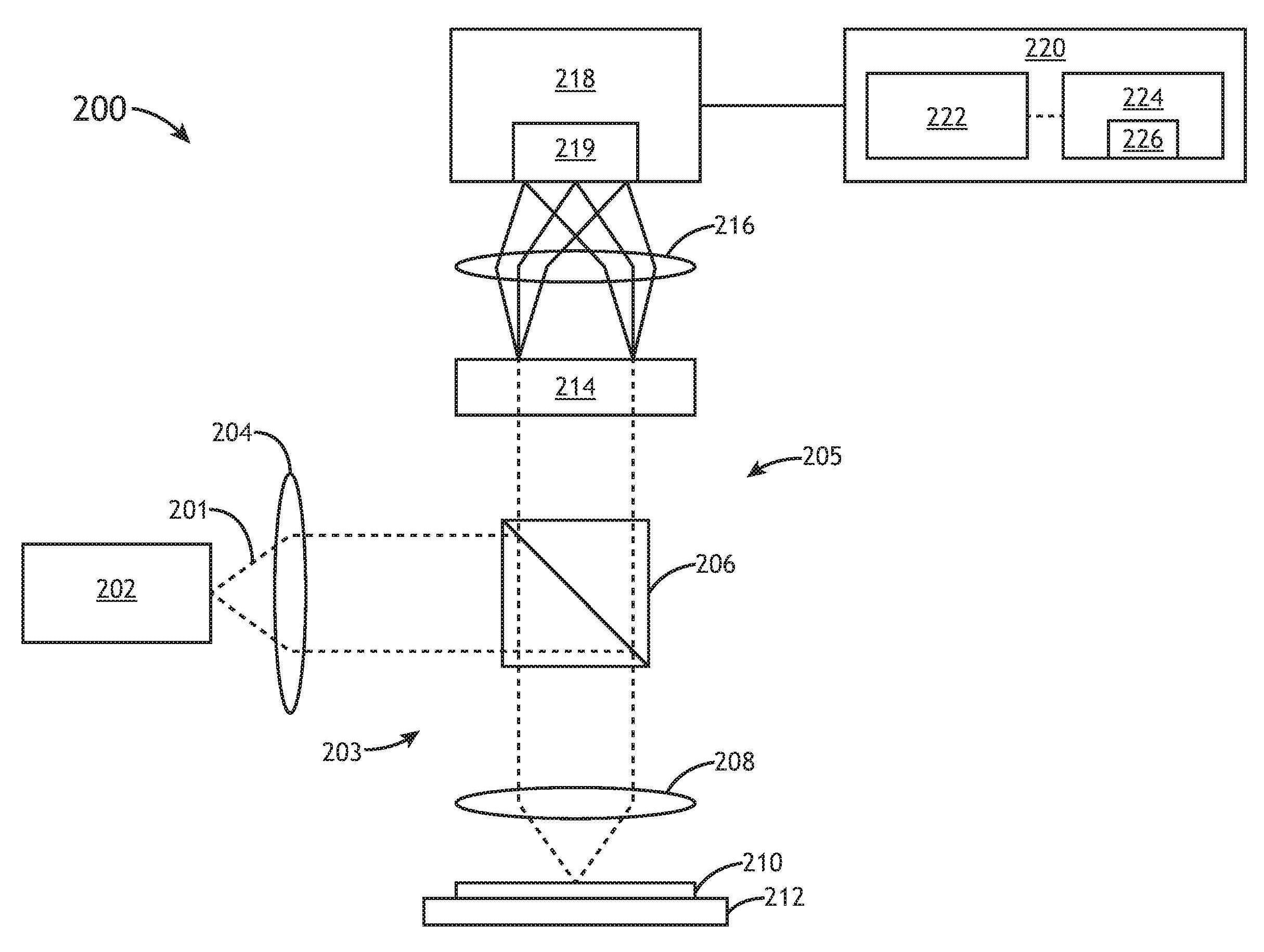
도 2는 본 개시의 하나 이상의 실시예에 따른, 분광 반사계에 기초한 산란측정 시스템(200)의 블록 다이어그램도를 예시한다. 일 실시예에서, 시스템(200)은 조명 광원(202), 조명 암(203), 수집 암(205), 분광계(214), 및 검출기 어셈블리(218)를 포함한다. 본 명세서에서 달리 언급되지 않는 한, 도 1의 시스템(100)과 연관된 설명이 도 2의 시스템(200)에 적용되는 것으로 간주될 수 있다는 점에 본 명세서에서 유의한다.2 illustrates a block diagram diagram of a
일 실시예에서, 시스템(200)은 샘플(210) 상의 다중 층 구조체 내의 적어도 2개의 층 사이의 오버레이 에러를 결정하도록 구성될 수 있다. 샘플(210)은 웨이퍼, 반도체 웨이퍼, 포토마스크 등을 포함하지만 이에 제한되지 않는, 본 기술 분야에서 알려진 임의의 샘플을 포함할 수 있다. 샘플(210) 내의 적어도 2개의 층이 전형적으로 적층된 주기적 구조체(예를 들어, 격자 구조체)를 포함한다는 점에 본 명세서에서 유의한다. 이와 관련하여, 샘플(210)이 샘플(210)의 층에 배치된 복수의 주기적 타깃 구조체(예를 들어, 격자 구조체)를 포함할 수 있으며, 각각의 주기적 타깃 구조체는 제1 층에 제1 구조체를 갖고 제2 층에 제2 구조체를 갖는다는 점에 본 명세서에서 추가로 유의한다. 다른 실시예에서, 샘플(210)은 제1 구조체와 제2 구조체 사이의 미리 정의된 오프셋을 포함할 수 있다.In one embodiment,
분광 반사측정법은 막 두께 및 오버레이와 같은 파라미터를 분석하기 위한 데이터를 획득하기 위해 다중 파장 또는 컬러의 광을 이용한다. 반사측정법은 반사 광의 측정이다. 오버레이 계측의 경우, 가시 영역 내의 파장 스펙트럼이 전형적으로 사용되는데, 그 이유는 가시 광이 반도체 산업에서 흔히 사용되는 재료들 중 다수를 통해 투과하기 때문이다. 막 표면 및 기판으로부터 반사된 광은 컴퓨터 및 알고리즘을 사용하여 분석된다. 분석은 막을 파괴하지 않거나 막과 접촉하지 않으면서 관심 파라미터를 산출한다. 분광 산란측정법은 다수의 파장을 사용하여 고정된 입사각(예를 들어, 수직 입사)에서 회절 응답을 측정하도록 설계된다. 이 메커니즘은, 분광 엘립소미터 및 분광 반사계 시스템과 같은, 박막 계측 장비를 사용하여 주기적 구조체들로부터 토포그래피 프로파일 정보를 정확하게 추출한다.Spectral reflectometry uses light of multiple wavelengths or colors to obtain data for analyzing parameters such as film thickness and overlay. Reflectometry is the measurement of reflected light. For overlay metrology, the wavelength spectrum in the visible region is typically used because visible light transmits through many of the materials commonly used in the semiconductor industry. The light reflected from the film surface and substrate is analyzed using computers and algorithms. The assay yields the parameter of interest without destroying or contacting the membrane. Spectral scatterometry is designed to measure the diffraction response at a fixed angle of incidence (eg, normal incidence) using multiple wavelengths. This mechanism accurately extracts topographic profile information from periodic structures using thin film metrology equipment, such as spectroscopic ellipsometer and spectroreflectometer systems.
일 실시예에서, 시스템(200)은 다수의 파장을 갖는 광학 입사 빔(예를 들어, 조명(201))을 생성하기 위한 조명 광원(202), 조명(201)을 콜리메이팅하기 위한 콜리메이팅 광학장치(204), 빔 스플리터(106), 조명을 샘플(210)로 지향시키고 샘플(210)로부터 반사되고 회절된 조명을 수집하는 대물 렌즈(208), 분광계(214), 및 입사 빔(예를 들어, 조명(201))에 응답하여 샘플(210)로부터 측정된 신호를 감지하기 위한 하나 이상의 센서(219)를 포함하는 검출기 어셈블리(218)를 포함한다.In one embodiment,
시스템(200)의 조명 광원(202)은 본 기술 분야에서 알려진 임의의 조명 광원을 포함할 수 있다. 예를 들어, 조명 광원(202)은 다수의 파장을 갖는 조명(201)을 생성하기 위한 광대역 조명 광원을 포함할 수 있다. 예를 들어, 조명 광원(202)은 백색 광원, 아크 램프, 무전극 램프, LSP(laser sustained plasma) 광원, 초연속체 광원(예를 들어, 광대역 레이저 광원) 등을 포함할 수 있지만, 이에 제한되지 않는다. LSP 광원의 예는 Energetiq Technology, Inc.로부터의 LSP 광원을 포함하지만 이에 제한되지 않는다. 초연속체 광원의 예는 NKT Photonics Inc.로부터의 초연속체 광원을 포함하지만 이에 제한되지 않는다. 조명 광원(202)은 또한 충분한 밝기를 갖는 조명(201)을 제공하도록 구성될 수 있다. 예를 들어, 조명 광원(202)은 대략 1 W/(nm cm2 sr)보다 큰 밝기를 갖는 조명(201)을 방출하도록 구성될 수 있다.The
반도체 계측 툴이 CMOS 제조에서 사용되는 상이한 재료 및 구조의 전부 또는 대부분에 대해 측정할 수 있다면 가장 유용하다는 것이 이해될 수 있다. 상이한 재료 및 구조는 서로 매우 상이한 반사율을 갖는다. 유연성을 갖기 위해, 반도체 계측 툴은 다중 파장 및/또는 다중 각도의 광 조명 및 광 수집을 사용할 수 있다. 이와 관련하여, 조명 광원(200)이 암시야 배향, 명시야 배향 등을 포함하지만 이에 제한되지 않는, 본 기술 분야에서 알려진 임의의 배향으로 구성될 수 있음에 본 명세서에서 유의한다. 게다가, 시스템(200)은 전력, 밝기, 스펙트럼 등을 포함하지만 이에 제한되지 않는, 조명 광원(202)의 하나 이상의 특성을 보정 및/또는 안정화시키기 위해 조명 광원(202)에 대한 빠른 피드백을 부가로 포함할 수 있다. 조명 광원(202)으로부터 방출된 조명(201)이 자유 공간 전파, 광섬유, 광 가이드 등을 포함하지만 이에 제한되지 않는, 본 기술 분야에서 알려진 임의의 수단에 의해 전달될 수 있다는 점에 유의한다.It can be appreciated that a semiconductor metrology tool would be most useful if it could measure for all or most of the different materials and structures used in CMOS fabrication. Different materials and structures have very different reflectivities from one another. For flexibility, semiconductor metrology tools may use multiple wavelengths and/or multiple angles of light illumination and light collection. In this regard, it is noted herein that the
다른 실시예에서, 시스템(200)은 조명(201)을 샘플(210)로 지향시키도록 구성된 조명 암(203)을 포함한다. 조명 암(203)은 본 기술 분야에서 알려진 임의의 수 및 유형의 조명 광학 컴포넌트를 포함할 수 있다. 일 실시예에서, 조명 암(203)은 조명(201)을 콜리메이팅하는 콜리메이팅 광학장치(204), 빔 스플리터(206), 및 조명(201)을 샘플(210)로 지향시키는 대물 렌즈(208)를 포함한다.In another embodiment, the
다른 실시예에서, 시스템(200)은 샘플(210)로부터 반사된, 회절된, 또는 산란된 조명(예를 들어, 방사선, 광)을 수집하도록 구성된 수집 암(205)을 포함한다. 다른 실시예에서, 수집 암(205)은 반사된 및/또는 산란된 조명을 분광계(214)로 지향 및/또는 집속시킬 수 있다. 분광계(214)가 수집된 조명을 복수의 파장으로 분리하고 수집된 조명을 검출기 어셈블리(218)의 복수의 센서(219)로 지향시키도록 구성된 분산 요소(dispersive element)(216)를 포함할 수 있다는 점에 본 명세서에서 유의한다. 이와 관련하여, 검출기 어셈블리(218)는 샘플(210) 상의 조명(201)의 입사 빔(들)에 응답하여 샘플(210)로부터 측정된 신호를 검출하도록 구성될 수 있다. 이와 관련하여, 검출기 어셈블리(218)로부터(예를 들어, 검출기 어셈블리(218)의 센서(219)로부터) 측정된 신호는 복수의 스펙트럼 신호를 포함할 수 있다.In another embodiment, the
다른 실시예에서, 검출기 어셈블리(218)는 하나 이상의 프로세서(222) 및 메모리(224)를 포함하는 제어기(220)에 통신 가능하게 결합된다. 다른 실시예에서, 하나 이상의 프로세서(222)는 메모리(224)에 통신 가능하게 결합될 수 있으며, 여기서 하나 이상의 프로세서(222)는 메모리(224)에 저장된 프로그램 명령어 세트를 실행하도록 구성된다. 일 실시예에서, 하나 이상의 프로세서(222)는 검출기 어셈블리(218)의 출력을 분석하도록 구성될 수 있다. 일 실시예에서, 프로그램 명령어 세트는 하나 이상의 프로세서(222)로 하여금 샘플(210)의 하나 이상의 특성을 분석하게 하도록 구성된다. 다른 실시예에서, 프로그램 명령어 세트는 하나 이상의 프로세서(222)로 하여금 샘플(210), 분광계(214), 및/또는 검출기 어셈블리(218) 상에 초점을 유지하기 위해 시스템(200)의 하나 이상의 특성을 수정하게 하도록 구성된다. 예를 들어, 하나 이상의 프로세서(222)는 조명 광원(202)으로부터의 조명(201)을 샘플(210)의 표면 상으로 집속시키기 위해 대물 렌즈(208) 또는 시스템(200)의 하나 이상의 광학 요소를 조정하도록 구성될 수 있다. 다른 예로서, 하나 이상의 프로세서(222)는 샘플(210)의 표면으로부터 산란된 및/또는 반사된 조명을 수집하고 수집된 조명을 분광계(214) 및/또는 검출기 어셈블리(218) 상에 집속시키기 위해 대물 렌즈(208) 및/또는 하나 이상의 광학 요소를 조정하도록 구성될 수 있다.In another embodiment, the
시스템(200)의 서브시스템들 중 임의의 것(예를 들어, 분광계(214), 센서(219), 검출기 어셈블리(218))에 의해 수행되는 것으로 이전에 설명된 분석 단계들 중 임의의 것이 부가적으로 및/또는 대안적으로 제어기(220)의 하나 이상의 프로세서(222)에 의해 수행될 수 있다는 점에 본 명세서에서 유의한다. 다른 실시예에서, 시스템(200)은 사용자 인터페이스(도시되지 않음)를 포함할 수 있다. 다른 실시예에서, 사용자 인터페이스는 디스플레이를 포함할 수 있다.Any of the analysis steps previously described as being performed by any of the subsystems of the system 200 (eg, the
시스템(200)의 요소가 단지 예시 목적으로 제공된다는 점과 본 개시의 사상 또는 범위를 벗어나지 않으면서 더 적은/부가의 요소가 시스템(200)에 존재할 수 있다는 점에 본 명세서에서 유의한다. 이와 관련하여, 시스템(200)이 하나 이상의 미러, 하나 이상의 렌즈, 하나 이상의 편광기, 하나 이상의 콜리메이터, 하나 이상의 파장판, 하나 이상의 센서, 하나 이상의 부가 검출기, 하나 이상의 카메라, 하나 이상의 개구 등을 포함하지만 이에 제한되지 않는 부가의 광학 요소를 포함할 수 있다는 점에 유의한다.It is noted herein that elements of
일 실시예에서, 산란측정 시스템(200)의 조명 광원(202)은 한번에 샘플(210) 상의 타깃 구조체의 단일 셀을 조명하도록 구성될 수 있다. 이와 관련하여, 인접한 셀들 사이의 신호 오염을 방지하기 위해 조명(201)을 단일 셀로 제한하기 위해 시야 조리개(도시되지 않음)가 조명 경로(예를 들어, 조명 암(203))에 배치될 수 있다. 게다가, 조명 개구 조리개(도시되지 않음)는 계측 신호로서 사용되는 회절 차수와 다른 회절 차수 사이의 중첩을 방지하기 위해 조명(201)을 충분히 작은 개구수(NA)로 제한하는 데 사용될 수 있다. 부가의 및/또는 대안의 실시예에서, 시스템(200)의 조명 광원(202)은 샘플(210) 상의 타깃 구조체의 다수의 셀을 한 번에 하나씩 조명하도록 구성될 수 있다.In one embodiment, the
다른 실시예에서, 조명 광원(202)은 선형 편광된 조명(201)으로 타깃 구조체의 다수의 셀을 조명하도록 구성될 수 있다. 일 실시예에서, 조명(201)이 샘플(210) 표면에 실질적으로 수직으로 입사하도록 조명 암(203)은 조명 광원(202)으로부터의 조명(201)을 샘플(210) 상으로 지향시키도록 구성된다. 이와 관련하여, 0차 회절 방사선이 파장의 함수로서 측정된다. 수직 입사에서, 샘플(210)의 층에 배치된 격자 구조체와 관련하여 다수의 편광각에 대해 다수의 반사율 스펙트럼이 획득될 수 있다는 점에 본 명세서에서 유의한다. 일 실시예에서, 샘플(210)로부터 산란된 조명을 수집하는 수집 암(205)의 요소(예를 들어, 대물 렌즈(208), 빔 스플리터(206) 등)는 수집 암(205)이 계측 조명을 분광계(214)로만 투과시키도록 구성된다.In another embodiment, the
다른 실시예에서, 산란된 조명은 이미징 모드 또는 비-이미징 모드 중 어느 하나에서 분광계(214)에 의해 분석된다. 전형적인 데이터 수집은 TE(transverse electric) 스펙트럼 및 TM(transverse magnetic) 스펙트럼 둘 모두를 포함한다. 이와 관련하여, 편광된 광을 사용하는 것은 TE 스펙트럼과 TM 스펙트럼 사이의 진폭 차이 및 위상 차이 둘 모두가 측정될 수 있기 때문에 향상된 민감도를 가능하게 한다는 점에 유의한다.In another embodiment, the scattered illumination is analyzed by the
도 3 및 도 4는 본 개시의 하나 이상의 실시예에 따른, 모델 기반 오버레이 계측(mOVL)을 위한 알고리즘(300, 400)을 예시한다. 알고리즘(300, 400)이 시스템(100) 및 산란측정 시스템(200)과 관련하여 사용될 수 있다는 점에 본 명세서에서 유의한다. 그렇지만, 부가의 또는 대안의 시스템 레벨 실시예가 알고리즘(300, 400)의 단계들의 전부 또는 일부를 수행할 수 있다는 점에서, 알고리즘(300, 400)이 시스템(100) 및 산란측정 시스템(200)으로 제한되지 않는다는 것이 추가로 인식된다.3 and 4 illustrate
일 실시예에서, 알고리즘(300, 400)의 역할은 측정된 신호(예를 들어, 검출기 어셈블리(218) 상에서 수집된 조명에 응답하여 측정된 신호)로부터 오버레이의 값을 추출하는 것이다. 이에 따라, 알고리즘(300, 400)의 본질이 신호의 속성, 따라서 사용된 특정 기술(예를 들어, 하드웨어, 소프트웨어)에 의존한다는 점에 유의한다.In one embodiment, the role of the
산란측정 시스템(예를 들어, 산란측정 시스템(200))에서, 타깃으로부터 잘 정의된 특정 회절 차수로 반사된 방사선의 강도는 연속 파라미터의 함수로서 측정된다. 분광 산란측정법에서는, 이 연속 파라미터가 반사된 방사선의 파장인 반면, 각도 분해 산란측정법에서는, 그것이 광이 타깃으로부터 회절되는 극각(polar angle) 및 방위각이다. 공간 분해능의 부족으로 인해, 산란측정 툴은 타깃의 다양한 셀을 순차적으로 측정할 수 있다. 이와 관련하여, 각각의 셀의 신호는 작은 스폿을 셀 상으로 집속시키고 강도를 분광계로 이미지면(image plane)에서 판독하는 것(예를 들어, 분광 산란측정법) 또는 CCD 또는 다른 이미지 센서로 동공면(pupil plane)에서 판독하는 것(예를 들어, 각도 분해 산란측정법) 중 어느 하나에 의해 측정될 수 있다. 따라서, 산란측정 신호는 강도를 타깃의 각각의 셀에 대해 개별적으로 측정된 관련 연속 파라미터의 함수로서 표현한다.In a scatterometry system (eg, scatterometry system 200 ), the intensity of radiation reflected from a target with a specific, well-defined diffraction order is measured as a function of a continuous parameter. In spectral scatterometry, this continuous parameter is the wavelength of the reflected radiation, whereas in angle resolved scatterometry, it is the polar angle and azimuth at which light is diffracted from the target. Due to the lack of spatial resolution, scatterometry tools can measure various cells of a target sequentially. In this regard, the signal of each cell can be obtained by focusing a small spot onto the cell and reading the intensity in the image plane with a spectrometer (eg, spectral scatterometry) or the pupil plane with a CCD or other image sensor. (eg, angle resolved scatterometry) in the pupil plane. Thus, the scatterometry signal expresses the intensity as a function of the relevant continuous parameter measured individually for each cell of the target.
오버레이 계측 타깃은 샘플(210)의 하나 이상의 층에 배치된 대용물 타깃 구조체(proxy target structure)이다. 오버레이 계측 타깃은 장치/시스템이 타깃의 적어도 두 번의 노광 사이의 오버레이 에러를 결정할 수 있게 한다. 원칙적으로, 오버레이 계측 타깃의 오버레이 에러의 결정은 다중 노출로부터의 정보를 포함할 수 있다. 오버레이 계측 타깃을 사이드 바이 사이드(side-by-side) 구조체 또는 격자 위 격자 구조체(grating-over-grating) 중 어느 하나로서 분류하는 것이 편리한다. 이들 경우 둘 모두에서, 계측 타깃은 복수의 셀을 포함한다. 사이드 바이 사이드 타깃의 경우에, 개별 셀은 전형적으로 단일 노출로부터의 정보를 포함하는 반면, 격자 위 격자 타깃의 경우에, 두 번의 노출로부터의 정보가 단일 셀에서 중첩된다. 일반적으로, 사이드 바이 사이드 타깃 설계는 이미징 센서와 호환되는 반면, 격자 위 격자 설계는 산란측정 센서와 호환되지만, 예외가 있을 수 있다.The overlay metrology target is a proxy target structure disposed on one or more layers of the
산란측정법 측정은 보통 최대 오버레이 민감도를 보장하기 위해 피치의 대략 25% 내지 35%로 설계된 시프트를 갖는 특수 설계된 타깃에 대해 수행된다. 수직 입사 편광 반사계(normal incident polarized reflectometer)의 경우에, TE 스펙트럼이 전형적으로 TM 스펙트럼보다 오버레이에 더 민감하다. 따라서, 민감도에 영향을 주지 않으면서 측정 시간을 감소시키기 위해, 보통 TE 스펙트럼만이 분석된다.Scatterometry measurements are usually performed on specially designed targets with a shift designed to approximately 25% to 35% of the pitch to ensure maximum overlay sensitivity. In the case of a normal incident polarized reflectometer, the TE spectrum is typically more sensitive to overlay than the TM spectrum. Therefore, in order to reduce the measurement time without affecting the sensitivity, usually only the TE spectrum is analyzed.
오버레이 타깃들 사이의 오버레이가 보통 차동 신호(differential signal) 접근법에 의해 신호(예를 들어, 검출기 어셈블리(218) 상에서 수집된 방사선에 응답하여 생성된 신호)로부터 추출된다는 점에 본 명세서에서 유의한다. 0차 산란측정법이 사용되는지 또는 1차 산란측정법이 사용되는지에 따라 알고리즘 및 타깃 설계가 실질적으로 상이하다는 점에 추가로 유의한다. 0차 산란측정법의 경우, 각각의 셀은 단일 0차 신호를 연속 파라미터의 함수로서 제공하는 반면, 1차 산란측정법(예를 들어, +1차 및 -1차)의 경우, 각각의 셀에 대해 2개의 신호가 연속 파라미터의 함수로서 측정된다. 이와 관련하여, 1차 산란측정법의 경우 더 적은 수의 셀이 요구되어, 잠재적으로 더 작은 타깃을 초래한다. 그렇지만, 1차 산란측정법은 일부 경우에 엄청난 비용이 들 수 있는데, 그 이유는 1차 산란측정법이 고도의 동공 균일성을 요구할 수 있고, 동공 불균일성의 영향을 감소시키는 교정 방법론의 강화된 품질을 요구할 수 있기 때문이다. 잔류 동공 불균일성 영향이 남아 있는 비-이상적인 경우에, 타깃 크기(1차 산란측정법에 유리함)와 성능(0차 산란측정법에 유리함) 사이의 절충이 있다.It is noted herein that the overlay between overlay targets is usually extracted from a signal (eg, a signal generated in response to radiation collected on detector assembly 218 ) by a differential signal approach. It is further noted that the algorithm and target design are substantially different depending on whether zero-order scatterometry or first-order scatterometry is used. For zero-order scatterometry, each cell provides a single zero-order signal as a function of a continuous parameter, whereas for first-order scatterometry (eg, +1 and -1), for each cell Two signals are measured as a function of a continuous parameter. In this regard, fewer cells are required for first order scatterometry, potentially resulting in a smaller target. However, primary scatterometry can be prohibitively expensive in some cases because primary scatterometry may require a high degree of pupil uniformity and will require enhanced quality of calibration methodologies to reduce the effects of pupil nonuniformity. because it can In the non-ideal case where residual pupil non-uniformity effects remain, there is a trade-off between target size (in favor of first-order scatterometry) and performance (in favor of zero-order scatterometry).
mOVL이 오버레이 부정확도 문제를 해결할 수 있다는 것이 본 명세서에서 인식된다. 예를 들어, mOVL은 부가 타깃을 추가할 필요가 없게 하면서 사인 오버레이 모델의 에러를 제거할 수 있다. 이 신규의 방법은 프로세스 변동 및 타깃 비대칭성의 존재에도 불구하고 정확한 오버레이 측정을 달성할 수 있다. 부가적으로, mOVL은 오버레이 정보 이외의 리소그래피/프로세스 정보를 제공할 수 있다. 예를 들어, 샘플(210)에 걸친 레지스트 프로파일의 변동이 mOVL을 사용하여 식별될 수 있다. 게다가, mOVL은 타깃 모델 셋업을 단순화할 수 있다. 이는 공칭 CD 값을 정확하게 추정하고, 민감도를 최적화하며, 파라미터 상관성을 감소시킬 수 있다.It is recognized herein that mOVL can solve the overlay inaccuracy problem. For example, mOVL can eliminate errors in the sine overlay model while eliminating the need to add additional targets. This novel method can achieve accurate overlay measurements despite the presence of process variations and target asymmetry. Additionally, mOVL may provide lithography/process information other than overlay information. For example, variations in resist profile across
2개의 mOVL 알고리즘 실시예가 본 명세서에서 설명된다. 즉, 2개의 mOVL 알고리즘 실시예는 실시간 회귀 및 라이브러리 기술을 포함한다. 이제 특히 도 3이 참조될 것이다.Two mOVL algorithm embodiments are described herein. That is, the two mOVL algorithm embodiments include real-time regression and library techniques. Reference will now be made in particular to FIG. 3 .
도 3은 본 개시의 하나 이상의 실시예에 따른, 산란측정 시스템에서 사용되는 모델 기반 오버레이 계측(mOVL)을 위한 실시간 회귀 기반 알고리즘(300)을 묘사하는 프로세스 흐름 다이어그램을 예시한다. 도 3에 예시된 바와 같이, 알고리즘(300)은 최소 제곱 문제를 다음과 같이 풀며:3 illustrates a process flow diagram depicting a real-time regression-based

여기서 ![]()
![]()
![]()
![]()
![]()
![]()
![]()
![]()
![]()
![]()
![]()
![]()
![]()
![]()
![]()
![]()
![]()
![]()
단계(302)에서, 신호 ![]()
![]()
![]()
![]()
![]()
![]()
단계(304)에서, 측정된 신호 ![]()
![]()
![]()
![]()
![]()
![]()
![]()
![]()
단계(306)에서, ![]()
![]()
단계(308)에서, ![]()
![]()
![]()
![]()
단계(304)로 돌아가서, ![]()
![]()
![]()
![]()
도 3에 묘사된 실시간 회귀 스킴이, 레시피를 셋업하는 데 시간을 거의 소요하지 않기 때문에, 연구 개발 단계에서 선호될 수 있다는 점에 본 명세서에서 유의한다. 반면에, 조사 중인 타깃이 복잡할 때, EM 솔버는 광학 응답을 계산하는 데 더 오랜 시간을 소요할 수 있으며, 도 4에 묘사된 것과 같은 라이브러리 기술 접근법이 더 적절할 수 있다.It is noted herein that the real-time regression scheme depicted in FIG. 3 may be preferred during the research and development phase as it takes little time to set up the recipe. On the other hand, when the target under investigation is complex, the EM solver may take longer to calculate the optical response, and a library description approach such as that depicted in FIG. 4 may be more appropriate.
도 4는 본 개시의 하나 이상의 실시예에 따른, 산란측정 시스템에서 사용되는 모델 기반 오버레이 계측(mOVL)을 위한 라이브러리 기술 기반 알고리즘(400)의 개념도를 예시한다.4 illustrates a conceptual diagram of a library technology-based
라이브러리 기술은 전형적으로 라이브러리 생성, 라이브러리 트레이닝, 및 측정을 포함한다. 예로서, mOVL에 대한 라이브러리 기술 기반 알고리즘은: 오버레이 모델을 셋업하는 것, 각도 분해 또는 스펙트럼 신호를 계산하는 것, 신호 및 오버레이 라이브러리를 생성하는 것, 및 라이브러리를 측정 신호에 적용하여 오버레이를 결정하는 것을 포함할 수 있다. 일 실시예에서, 알고리즘(400)은 라이브러리 생성(410), 라이브러리 트레이닝(420), 및 측정(430)을 포함하지만 이에 제한되지 않는, 라이브러리 기술 기법을 이용한다.Library techniques typically include library creation, library training, and measurement. As an example, library description based algorithms for mOVL include: setting up an overlay model, calculating an angular decomposition or spectral signal, generating a library of signals and overlays, and applying the library to a measurement signal to determine overlay. may include In one embodiment, the
일 실시예에서, 라이브러리 생성(410)은 관심 파라미터(411)의 샘플을 생성하는 것 및 전자기(EM) 솔버(412)를 사용하여 합성 신호(413)를 생성하는 것을 포함한다.In one embodiment,
관심 파라미터(예를 들어, ![]()
![]()
일 실시예에서, 도 4에 묘사된 바와 같이, 관심 파라미터(예를 들어, ![]()
![]()
![]()
![]()
![]()
![]()
다른 실시예에서, 알고리즘(400)은 라이브러리 트레이닝(420)을 포함한다. 라이브러리 트레이닝(420)에서, (411로부터의) 파라미터(423)를 (413으로부터의) 합성 신호(421)에 관련시키기 위해, 신경 네트워크와 같은, 머신 러닝 모델(422)이 사용된다. 이 프로세스는 ![]()
![]()
![]()
![]()
![]()
![]()
![]()
![]()
다른 실시예에서, 알고리즘(400)은 측정(430)을 포함한다. 일 실시예에서, 측정된 신호(431)가 먼저 계측 시스템(예를 들어, 시스템(200))으로부터 획득된다. 이와 관련하여, 측정된 신호(431)가 시스템 노이즈를 포함할 수 있다는 점에 유의한다. 다른 실시예에서, 측정된 신호(431)는 이어서 머신 러닝 모델(432)(예를 들어, 머신 러닝 모델(422)로부터 획득된 머신 러닝 모델(432))에 공급된다. 다른 실시예에서, 머신 러닝 모델(432)의 출력은 오버레이 결과(433)(예를 들어, 측정된 출력 ![]()
![]()
![]()
![]()
![]()
![]()
주성분 분석(principal component analysis)과 같은 차원 축소(dimensionality reduction) 기법이 행렬 ![]()
![]()
![]()
![]()
본 명세서에서 설명된 시스템, 방법, 및 알고리즘의 다양한 실시예가 단지 예시를 위한 것이며, 본 개시의 범위를 설명된 특정 실시예로 제한하는 것으로 의도되지 않는다는 점에 추가로 유의한다. 따라서, 본 명세서에서 설명된 오버레이 계측 시스템, 방법, 및 알고리즘이 도시되고 설명된 특정 실시예로 제한되는 것으로 의도되지 않으며, 본 명세서에서 개시된 원리 및 신규의 특징과 부합하는 가장 넓은 범위를 부여받아야 한다.It is further noted that the various embodiments of the systems, methods, and algorithms described herein are for illustrative purposes only and are not intended to limit the scope of the present disclosure to the specific embodiments described. Accordingly, the overlay metrology systems, methods, and algorithms described herein are not intended to be limited to the specific embodiments shown and described, but are to be accorded the widest scope consistent with the principles and novel features disclosed herein. .
예를 들어, 다음과 같은 기기들의 임의의 조합이 샘플의 제1 층에 형성된 제1 구조체와 제2 층에 형성된 제2 구조체 - 제1 구조체와 제2 구조체 사이에 미리 정의된 오프셋이 있음 - 를 각각 갖는 복수의 주기적 타깃에 대한 광학 신호를 측정하는 데 사용될 수 있다: 이미징 반사계, 이미징 분광 반사계, 편광 분광 이미징 반사계, 스캐닝 반사계 시스템, 병렬 데이터 취득이 가능한 2개 이상의 반사계를 가진 시스템, 병렬 데이터 취득이 가능한 2개 이상의 분광 반사계를 가진 시스템, 병렬 데이터 취득이 가능한 2개 이상의 편광 분광 반사계를 가진 시스템, 스테이지 장치를 이동시키는 일 또는 임의의 광학 요소 또는 반사계 스테이지를 이동시키는 일 없이 직렬 데이터 취득이 가능한 2개 이상의 편광 분광 반사계를 가진 시스템, 이미징 분광계, 파장 필터를 가진 이미징 시스템, 장파장 통과(long-pass) 파장 필터를 가진 이미징 시스템, 단파장 통과(short-pass) 파장 필터를 가진 이미징 시스템, 파장 필터가 없는 이미징 시스템, 간섭측정 이미징 시스템, 이미징 엘립소미터, 이미징 분광 엘립소미터, 스캐닝 엘립소미터 시스템, 병렬 데이터 취득이 가능한 2개 이상의 엘립소미터를 가진 시스템, 웨이퍼 스테이지를 이동시키는 일 또는 임의의 광학 요소 또는 엘립소미터 스테이지를 이동시키는 일 없이 직렬 데이터 취득이 가능한 2개 이상의 엘립소미터를 가진 시스템, Michelson 간섭계, Mach-Zehnder 간섭계, Sagnac 간섭계, 스캐닝 입사각 시스템, 및 스캐닝 방위각 시스템.For example, any combination of the following devices can generate a first structure formed in a first layer and a second structure formed in a second layer of the sample, with a predefined offset between the first structure and the second structure. It can be used to measure optical signals for multiple periodic targets each having: an imaging reflectometer, an imaging spectroreflectometer, a polarization spectroscopic imaging reflectometer, a scanning reflectometer system, with two or more reflectometers capable of parallel data acquisition. system, system with two or more spectroreflectometers capable of parallel data acquisition, system with two or more polarization spectroreflectometers capable of parallel data acquisition, moving the stage device or moving any optical element or reflectometer stage Systems with two or more polarization spectroreflectometers, imaging spectrometers, imaging systems with wavelength filters, imaging systems with long-pass wavelength filters, short-pass Imaging system with wavelength filter, imaging system without wavelength filter, interferometric imaging system, imaging ellipsometer, imaging spectroscopic ellipsometer, scanning ellipsometer system, system with two or more ellipsometers capable of parallel data acquisition , systems with two or more ellipsometers that allow serial data acquisition without moving the wafer stage or moving any optical element or ellipsometer stage, Michelson interferometer, Mach-Zehnder interferometer, Sagnac interferometer, scanning angle of incidence system, and a scanning azimuth system.
도 5는 본 개시의 하나 이상의 실시예에 따른, 고품질 현미경 대물 렌즈(508) 및 튜브 렌즈(516)를 포함하는 오버레이 계측 시스템(500)의 단순화된 개략도를 예시한다. 일 실시예에서, 계측 시스템(500)은 튜브 렌즈(516), 현미경 대물 렌즈(508), 및 검출기 어셈블리(518)를 포함한다. 일 실시예에서, 시스템(500)은 샘플(510)을 측정 또는 검사하도록 구성된다. 본 명세서에서 달리 언급되지 않는 한, 도 1 및 도 2의 시스템(100, 200)과 연관된 설명이 도 5의 계측 시스템(500)에 적용되는 것으로 간주될 수 있다는 점에 본 명세서에서 유의한다.5 illustrates a simplified schematic diagram of an
일 실시예에서, 계측 시스템(500)은 현미경 대물 렌즈(508) 및 튜브 렌즈(516)를 포함하는 에피 조명 현미경(epi-illuminated microscope)과 비슷하다. 샘플(510)의 표면 상의 오버레이 타깃이 대물 렌즈(508)에 의해 검출기 어셈블리(518) 상으로 이미징된다. 검출기 어셈블리(518)는 CCD, 이미지 센서, 및 분광계를 포함하지만 이에 제한되지 않는, 본 기술 분야에서 알려진 임의의 검출기 어셈블리를 포함할 수 있다. 일 실시예에서, 계측 시스템(500)의 광학 요소는 정확한 오버레이 측정을 가능하게 하기 위해 색수차 및 비대칭 수차를 최소화하도록 설계된다.In one embodiment,
일 실시예에서, 조명은 대물 렌즈(508)를 통해 지향되어 샘플(510)의 표면 상으로 집속된다. 다른 실시예에서, 대물 렌즈(508)는 고 개구수(NA) 대물 렌즈(즉, 대략 0.9 이상의 NA를 가짐)이다. 이와 관련하여, 대물 렌즈(508)로부터 샘플(510) 상으로 방출되는 조명 광선은 상대적으로 큰 원추각을 채운다. 0.9 NA는 arcsin(0.90) ![]()
![]()
시스템(500)이 오버레이 계측을 위해 사용될 때, 대물 렌즈(508)는 샘플(510)에서 텔레센트릭(telecentric)일 수 있고, 매우 낮은 배율 색수차(lateral chromatic aberration)(예를 들어, 측정되는 구조체에 대응하는 시야에 걸쳐 대략 20nm 미만의 배율 색수차, 바람직하게는 대략 10nm 미만)를 가질 수 있다. 일 실시예에서, 대물 렌즈(508)의 텔레센트리시티(telecentricity)는 5 mrad(milli-radians) 미만일 수 있다. 예로서, 대물 렌즈(508)의 텔레센트리시티는 의도된 동작의 전체 파장 범위(전형적으로 적어도 400nm 내지 800nm에 걸친 파장 범위)에 걸쳐 대략 2mrad 이하일 수 있다. 오버레이 계측의 경우, 보통 대략 5μm 내지 대략 40μm의 측면 치수를 가진 구조체에 대해 측정이 이루어진다. 이와 관련하여, 10μm 내지 50μm의 측면 치수를 가진 대물 렌즈(508)의 시야의 중앙 부분에 대해 수차 사양이 가장 크리티컬하다. 대물 렌즈(508)의 시야의 이 중앙 부분은 본 명세서에서 "임계 시야(critical field of view)"라고 지칭된다. "임계 시야" 밖에 있는 대물 렌즈(508)의 외부 영역이 덜 크리티컬하고, 이러한 외부 영역에서의 더 큰 수차가 허용될 수 있다는 것이 이해될 수 있다. 대물 렌즈(508)에 대한 더 상세한 설명은 Chuang 등의 미국 특허 제7,245,438호 및 제7,474,461호에서 발견될 수 있다. 이들 특허는 참조에 의해 전체가 본 명세서에 포함된다.When
다른 실시예에서, 샘플(510)에 의해 반사된, 회절된, 또는 산란된 광은 대물 렌즈(508)에 의해 수집되고, 대물 렌즈(508)는 수집된 조명을 빔 스플리터(502 및 504)를 통해 튜브 렌즈(516)로 지향시키도록 구성된다. 이와 관련하여, 2개의 빔 스플리터(502 및 504)는 광학 경로에서 대물 렌즈(508)와 튜브 렌즈(516) 사이의 위치된다. 일 실시예에서, 제1 빔 스플리터(예를 들어, 빔 스플리터(502 또는 504))는 에피 조명(epi-illumination)을 위해 조명 광원(도시되지 않음)으로부터의 조명을 대물 렌즈(508)로 지향시키도록 구성될 수 있다. 다른 실시예에서, 제2 빔 스플리터(예를 들어, 빔 스플리터(502 또는 504))는 Linnik 간섭계의 기준 암을 형성하도록 또는, 대안적으로, 대물 렌즈(508)에 의해 수집된 조명의 일 부분을 오토포커스 센서로 지향시키도록 구성될 수 있다. 빔 스플리터(502, 504)에 대한 더 철저한 설명은 도 1 및 그의 연관된 설명을 참조하면 발견될 수 있다. 도 5에 묘사된 요소는 물론, 그의 부수적 설명이 단지 설명적이고 예시적인 것임에 유의한다. 이와 관련하여, 본 개시의 사상 및 범위를 벗어나지 않으면서 광학 요소의 대안적인 배열이 구현될 수 있다. 예를 들어, 대안의 실시예에서, 단일 빔 스플리터는 빔 스플리터(502 및 504)의 기능을 수행하도록 구성될 수 있다.In another embodiment, the light reflected, diffracted, or scattered by the
일 실시예에서, 샘플(510)로부터 반사된, 회절된, 또는 산란된 조명은 빔 스플리터(502, 504)를 통해 튜브 렌즈(516)로 지향된다. 일 실시예에서, 튜브 렌즈(516)는 샘플(510) 표면의 이미지를 검출기 어셈블리(518) 상에 생성하도록 구성된다. 다른 실시예에서, 튜브 렌즈(516)는 동시에 샘플(510) 표면의 이미지를 검출기 어셈블리(518) 상에 생성하고 대물 렌즈(508)의 동공 조리개의 이미지를 위치(501)에 생성하도록 구성된다. 튜브 렌즈(516)는 대물 렌즈(508)의 배율 색수차와 비교하여 최소한의 배율 색수차를 생성하도록 추가로 구성될 수 있다(즉, 대물 렌즈(508)의 임계 시야에 대해 튜브 렌즈(516)의 배율 색수차는 수 nm 이하임). 일 실시예에서, 튜브 렌즈(516)는 샘플(510) 표면의 이미지의 배율 색수차 및 동공 조리개의 이미지(501)의 배율 색수차가 작도록 구성된다(즉, 대물 렌즈(508)의 임계 시야에 대한 물체면(object plane)에서 샘플(510) 표면의 이미지의 배율 색수차는 수 nm 이하이고, 동공 조리개의 이미지의 배율 색수차는 동공 조리개의 501에서의 이미지의 직경의 몇 퍼센트 미만, 예컨대, 약 1% 이하이다). 다른 실시예에서, 튜브 렌즈(516)는 검출기 어셈블리(518) 상의 이미지 및 위치(501)에서의 동공 조리개의 이미지 둘 모두에 대해 최소(즉, 대략 200μm 미만 또는 대략 100μm 미만)의 축상 색수차(axial chromatic aberration)를 생성하도록 구성된다. 이 실시예에서, 튜브 렌즈(630)는 대물 렌즈(508)의 축상 색수차에, 기껏해야, 약간의 변화를 야기하며, 이는 대물 렌즈(508)가 낮은 축상 색수차를 갖는 경우에 유리하다.In one embodiment, reflected, diffracted, or scattered illumination from
다른 실시예에서, 대물 렌즈(508)는 위치(501)에서의 동공 조리개의 이미지 및 검출기 어셈블리(518) 상의 이미지 둘 모두에 대해 낮은 배율 색수차를 갖도록, 그리고 검출기 어셈블리(518) 상의 이미지에 대해서는 낮은 축상 색수차를 갖지만 위치(501)에서의 동공의 이미지에 대해서는 200μm보다 큰, (튜브 렌즈(516)에 의해 보상되지 않는 경우) 어쩌면 수 mm만큼 큰 축 색수차를 갖도록 구성된다. 이 실시예에서, 튜브 렌즈(516)는 위치(501)에서의 동공 조리개의 이미지 및 검출기 어셈블리(518) 상의 이미지 둘 모두에 대해 낮은 배율 색수차를 갖도록, 그리고 검출기 어셈블리(518) 상의 이미지에 대해서는 낮은 축상 색수차를 갖지만, 동공 조리개의 이미지에 대한 대물 렌즈(508)의 축상 색수차를 실질적으로 제거하는 동공의 이미지에 대한 축상 색수차를 갖도록 구성된다(즉, 대물 렌즈(508)와 튜브 렌즈(516)의 조합으로 인한 위치(501)에서의 동공 조리개의 이미지에 대한 결과적인 축상 색수차는 대략 200μm 미만 또는 대략 100μm 미만임). 이 실시예의 장점은 대물 렌즈(508)가, 대물 렌즈(508)의 동공 조리개의 위치(501)에서의 이미지의 축상 색수차를 또한 동시에 최소화하려고 시도하는 부가의 제약 없이, 검출기 어셈블리(518) 상의 이미지의 배율 색수차 및 축상 색수차와 대물 렌즈(508)의 동공 조리개의 위치(501)에서의 이미지의 배율 색수차를 동시에 최소화하도록 구성될 수 있다는 것이다. 위치(501)에서의 동공 조리개의 이미지가 전형적으로 대략 10mm의 직경을 가질 것이기 때문에, 동공 조리개의 이미지에 대한 배율 색수차는 이 위치에 배치될 수 있는 개구의 제조 공차에 비해 작아야 한다(즉, 10mm 직경 이미지에 대해 100μm 미만, 대략 50μm 미만, 또는 대략 20μm 미만이어야 함). 유리하게도, 이러한 구성은 계측 시스템(500)의 전체적으로 더 낮은 레벨의 색수차를 초래할 수 있다.In another embodiment, the
위에서 설명된 실시예들 둘 모두가 광대역 축상 색 보정(broadband axial chromatic correction)을 가능하게 하면서 동시에 낮은 레벨의 배율 색수차를 달성할 수 있다는 점에 본 명세서에서 유의한다. 부가적으로, 대물 렌즈(508) 및 튜브 렌즈(516)를 포함하는 계측 시스템(500)은 이미지 색수차 및 동공 색수차 둘 모두에 대해 보정된다. 대물 렌즈(508) 및 튜브 렌즈(516)가 본 명세서에서 설명된 바와 같이 구성될 때 상이한 파장에 대해 대물 렌즈(508)의 동공 조리개의 이미지의 위치(501)가 시프트되지 않는다는 점에 추가로 유의한다. 종래의 튜브 렌즈가 축상 색수차를 보정할 수 있지만, 튜브 렌즈(516)의 배율 색수차는 대물 렌즈(508)의 배율 색수차보다 더 나쁠 수 있다. 게다가, 종래의 튜브 렌즈는 검출기 어셈블리(518) 상의 이미지의 배율 수차 및 축상 수차를 보정할 수는 있지만, 동공 조리개의 위치(501)에서의 이미지의 수차를 보정하지는 못한다(또는 수차를 유입시킬 수 있음). 비교해서 말하면, 본 개시의 시스템(500)은, 튜브 렌즈(516)가 배율 색수차를 열화시키지 않으면서 그의 축상 색수차를 보정할 수 있다는 사실로 인해, 이미지 및 동공 중 어느 하나 또는 둘 모두에 대한 수백 μm의 축상 색수차가 허용될 수 있기 때문에, 대물 렌즈(508)의 배율 색수차가 단지 몇 nm 이하로 감소되도록 할 수 있다.It is noted herein that both of the embodiments described above can achieve a low level of chromatic aberration of magnification while enabling broadband axial chromatic correction. Additionally,
일 실시예에서, 대물 렌즈(508)의 동공 조리개(도시되지 않음)의 이미지가 제2 검출기(도시되지 않음)로 지향될 수 있도록 하기 위해, 튜브 렌즈(516)와 검출기 어셈블리(518) 사이에 빔 스플리터 또는 플립인 미러(flip-in mirror)(도시되지 않음)가 배치된다. 다른 실시예에서, 시스템(500)은 하나 이상의 프로세서(도시되지 않음)를 가진 제어기(도시되지 않음)를 포함한다. 이 실시예에서, 하나 이상의 프로세서(도시되지 않음)는 튜브 렌즈(516)와 검출기 어셈블리(518) 사이의 조명 경로 내로의 렌즈(도시되지 않음)의 삽입을 제어할 수 있으며, 렌즈는 대물 렌즈(508)의 동공 조리개의 이미지를 검출기 어셈블리(518) 상에 형성하도록 구성된다.In one embodiment, between the
계속해서 도 5를 참조하면, 도 5는 검출기 어셈블리(518) 상의 샘플(510) 표면의 이미지 및 대물 렌즈(508)의 동공 조리개의 위치(501)에서의 이미지의 낮은 배율 색수차 및 축상 색수차를 동시에 달성하도록 구성된 계측 시스템(500)을 예시한다. 이 실시예에서, 튜브 렌즈(516)는 더블릿(doublet)(524), 렌즈(526, 528, 및 530), 및 트리플릿(triplet)(532)을 포함하는 다수의 렌즈 요소를 포함한다. 일 실시예에서, 더블릿(524), 렌즈(526), 및 렌즈(528)는 샘플(510) 표면의 중간 이미지를 위치(503)에 생성하도록 구성된다. 다른 실시예에서, 렌즈(530) 및 트리플릿(532)은 검출기 어셈블리(518) 상에 최소한의 수차를 갖는 샘플(510) 표면의 이미지를 생성하도록 구성된다(즉, 렌즈(530) 및 트리플릿(532)은 위치(503)에서의 중간 이미지의 임의의 수차를 실질적으로 제거하도록 구성됨). 트리플릿(532)이 튜브 렌즈(516)의 구성에서 추가적인 자유도를 제공하기 위해 작은 에어 갭을 포함할 수 있다는 점에 유의한다.With continued reference to FIG. 5 , FIG. 5 shows simultaneous low magnification chromatic aberration and axial chromatic aberration of an image of the surface of
종래의 튜브 렌즈는 위치(503)에 샘플(510)의 표면의 중간 이미지를 생성하도록 구성된 더블릿 또는 트리플릿(예컨대, 더블릿(524)), 및 위치(503)에서의 중간 이미지의 검출기 어셈블리(518)에서의 이미지를 생성하도록 구성된 다른 더블릿 또는 트리플릿(예컨대, 트리플릿(532))으로 구성될 수 있다. 그렇지만, 종래의 튜브 렌즈는 샘플(510) 표면 및 동공 조리개 둘 모두의 이미지의 낮은 배율 색수차 및 축상 색수차를 동시에 달성하도록 구성되기에 충분한 자유도를 갖지 않는다. 게다가, 종래의 튜브 렌즈는 또한 원하는 위치(501)에 동공 조리개의 이미지를 배치하도록 구성되기에 충분한 자유도를 갖지 않을 수 있다. 이와 관련하여, 검출기 어셈블리(518)에서 이미지의 위치의 최소한의 시프트를 야기하면서 동공 조리개의 이미지의 위치를 변경하기 위해 중간 이미지의 위치(예를 들어, 위치 503)에 시야 렌즈(field lens)가 배치될 수 있다는 것은 잘 알려져 있다. 그렇지만, 시야 렌즈는 그의 표면이 검출기 어셈블리(518) 상에 실질적으로 초점이 맞춰져 있음으로써 그의 표면 상의 임의의 결함이 검출기 어셈블리(518) 상의 이미지의 품질을 열화시킨다는 잘 알려진 단점을 갖는다.A conventional tube lens includes a doublet or triplet (eg, doublet 524) configured to produce an intermediate image of the surface of the
일 실시예에서, 튜브 렌즈(516)는 위치(501)에서의 대물 렌즈(508)의 동공 조리개의 이미지의 위치를 제어하도록 구성된 렌즈(528 및 530)를 포함하는 한편, 다른 렌즈 요소와 조합하여, 위치(501)에서의 동공 이미지 및 검출기 어셈블리(518) 상의 이미지의 낮은 배율 색수차 및 축상 색수차를 보장한다. 일 실시예에서, 도 5에 예시된 바와 같이, 렌즈(530)는 주변 광선과 주 광선이 렌즈(530)와 트리플릿(532)의 실질적으로 대향 측면을 통과하도록 보장하기 위해 네거티브 렌즈(negative lens)로서 구성된다. 이와 관련하여, 예시된 바와 같이, 주 광선은 트리플릿(532) 및 렌즈(530)의 하부 측면을 통과하는 반면, 주변 광선은 트리플릿(532) 및 렌즈(530)의 상부 측면을 통과한다. 비교해서 말하면, 주 광선과 주변 광선 둘 모두가 더블릿(524)과 렌즈(526)의 동일한 측면(즉, 예시된 바와 같이 하부 측면)을 통과한다.In one embodiment,
일 실시예에서, 광선 다발(ray bundle)(520)은 대물 렌즈(508)의 시야의 중심에서 시작되는 광선을 묘사한다. 광선 다발(520) 내의 광선은 검출기 어셈블리(518) 상의 이미지의 중심에 집속될 수 있다. 다른 실시예에서, 광선 다발(520)은, 대물 렌즈(508)의 동공 조리개를 간신히 터치하는 시야의 중심으로부터의 광선인, 주변 광선을 포함한다.In one embodiment,
다른 실시예에서, 광선 다발(522)은 대물 렌즈(508)의 임계 시야의 하나의 에지에서 시작되는 광선을 예시한다. 광선 다발(522) 내의 광선은 검출기 어셈블리(518) 상의 이미지의 중심으로부터 떨어져 있는 지점에 집속될 수 있다. 일 실시예에서, 광선 다발(522)은, 대물 렌즈(508)의 동공의 중심을 통과하는 대물 렌즈(508)의 임계 시야의 에지로부터의 광선인, 주 광선을 포함한다(즉, 주 광선은 예시된 바와 같이 다발(522)의 중심에 있는 광선임). 축상 색수차에 대한 광학 표면의 기여가 주변 광선이 해당 표면을 통과할 때 주변 광선의 높이의 제곱에 비례하는 반면, 배율 색수차에 대한 해당 표면의 기여는 주변 광선 및 주 광선이 해당 표면을 통과할 때 주 광선의 높이와 주변 광선의 높이의 곱에 비례한다는 점에 본 명세서에서 유의한다. 이와 관련하여, 튜브 렌즈(516)가 튜브 렌즈(516) 내의 위치(503)에서의 중간 이미지의 양쪽에 있는 렌즈 요소에서의 주변 광선의 높이와 주 광선의 높이의 곱의 반대 부호로 인해 최소한의 배율 색수차 및 축상 색수차를 갖도록 구성될 수 있다는 점에 추가로 유의한다.In another embodiment, the
계속해서 도 5를 참조하면, 다른 실시예에서, 튜브 렌즈(516)는 주변 광선이 더블릿(524) 및 렌즈(526)의 광학 축(예를 들어, 중심)에 가깝게 통과하는 반면, 주 광선이 광학 축으로부터 상당히 더 멀리 떨어져 통과하도록 추가로 구성될 수 있다. 이 실시예에서, 튜브 렌즈(516)는, 위치(501)에서의 동공 이미지와 검출기 어셈블리(518) 상의 이미지 둘 모두의 낮은 배율 색수차 및 검출기 어셈블리(518) 상의 이미지의 낮은 축상 색수차를 유지하면서, 동공 이미지의 상당한 축상 색수차(예를 들어, 대략 100μm 초과)를 생성하도록 구성될 수 있다. 이 실시예에서, 튜브 렌즈(516)는 그의 동공 축상 색수차가 대물 렌즈(508)의 동공 축상 색수차를 실질적으로 제거하도록(예를 들어, 대략 200μm 미만으로 또는 대략 100μm 미만으로 감소시키도록) 구성된다. 동공 축상 색수차의 이러한 감소가 가능한 이유는 주변 광선의 역할과 주 광선의 역할이 샘플(510) 표면의 이미지와 동공의 이미지 사이에서 상호교환되기 때문이다. 환언하면, 샘플(510) 표면의 이미지의 주변 광선은 동공의 이미지의 주 광선이고, 그 반대의 경우도 마찬가지이다. 이와 관련하여, 이미지 주 광선(즉, 동공 이미지의 주변 광선)이 광학 축으로부터 상당히 변위되어 더블릿(524) 및 렌즈(526)의 표면을 통과하도록 튜브 렌즈(516)가 구성되기 때문에, 다른 수차를 작게 유지하면서 (대물 렌즈(508)의 대응하는 수차를 실질적으로 제거하기 위해) 적절한 양의 동공 축상 색수차가 생성될 수 있다.With continued reference to FIG. 5 , in another embodiment,
다른 실시예에서, 시스템(500)은 수집된 조명의 일 부분을 거부(reject)하도록 구성된, 위치(503)에 있는 시야 조리개를 포함한다. 이 시야 조리개는, 도 1 및 도 2에 도시된 바와 같은, 제어기의 하나 이상의 프로세서를 통해 삽입, 제거, 또는 조정될 수 있다. 이와 관련하여, 위치(503)에 있는 시야 조리개는 계측 시스템의 수집 암(예를 들어, 수집 암(105, 205))에서 사용된다. 산란측정 오버레이 시스템의 경우, 신호 오염과 동공 이미징 분해능 사이에서 절충하기 위해, 샘플(510) 표면의 주어진 타깃 크기에 대해 시야 조리개 크기가 최적화될 수 있다.In another embodiment,
일 실시예에서, 조명 동공에서의 개구는 대물 렌즈(508)의 개구수의 각도들의 하나의 서브세트를 조명하도록 구성될 수 있는 반면, 위치(501)에 있는 수집 동공에서의 다른 개구는 개구수의 각도들의 실질적으로 비-중첩하는 서브세트로부터의 조명을 수집하도록 구성될 수 있다. 이와 관련하여, 회절된 또는 산란된 조명은 경면 반사를 실질적으로 차단하면서 수집될 수 있어, 그에 의해 암시야 이미지를 생성할 수 있다. 예를 들어, 실질적인 차단은 샘플(510) 표면으로부터 경면 반사된 조명 파워(illumination power)의 90% 이상을 차단하는 것을 포함할 수 있다.In one embodiment, the aperture in the illumination pupil may be configured to illuminate one subset of the angles of the numerical aperture of the
도 1을 참조하여 위에서 설명된 바와 같이, 검사 및/또는 계측 시스템(100)의 일 실시예에서, 조명 경로는 튜브 렌즈(516)와 유사한 튜브 렌즈로 구성될 수 있다. 일 실시예에서, 조명 경로 내의 튜브 렌즈는, 제어기(120)의 하나 이상의 프로세서(122)에 의해 추가로 제어될 수 있는, 위치(501 및/또는 503)와 공액인 위치에 있는 개구로 구성될 수 있다. 제어기(120)의 하나 이상의 프로세서(122)는 관심 피처에 대한 검사 또는 계측 시스템(100)의 민감도를 증가시키면서, 막 층의 두께의 변동과 같은, 관심 대상이 아닌 샘플(110)의 다른 피처에 대한 민감도를 감소시키기 위해 조명 경로 및 수집 경로 내의 개구를 제어할 수 있다.As described above with reference to FIG. 1 , in one embodiment of the inspection and/or
도 6은 본 개시의 하나 이상의 실시예에 따른, 다수의 측정 서브시스템을 포함하는 계측 시스템(600)의 단순화된 개략도를 예시한다. 시스템(600)이 본 명세서에서 개시된 시스템, 알고리즘, 또는 실시예 중 하나 이상을 구현하도록 구성될 수 있음이 본 명세서에서 고려된다.6 illustrates a simplified schematic diagram of a
일 실시예에서, 계측 시스템(600)은 빔 프로파일 엘립소미터(Beam Profile Ellipsometer; BPE)(610), 빔 프로파일 반사계(Beam Profile Reflectometer; BPR)(612), 광대역 반사 분광계(Broadband Reflective Spectrometer; BRS)(614), 심자외선 반사 분광계(Deep Ultra Violet Reflective Spectrometer; DUV)(616), 광대역 분광 엘립소미터(Broadband Spectroscopic Ellipsometer; BSE)(618), 및 기준 엘립소미터(602)를 포함한다. 다른 실시예에서, 시스템(600)은 레이저(620), 레이저(690), 및 조명 광원(102)을 포함한다. 다른 실시예에서, 레이저(620)는 프로브 빔(624)을 생성할 수 있고, 조명 광원(102)은 프로브 빔(626)을 생성할 수 있다. 프로브 빔(626)은 렌즈(628)에 의해 콜리메이팅되어 미러(629)에 의해 프로브 빔(624)과 동일한 경로를 따라 지향될 수 있다. 일 실시예에서, 레이저(520)는 670 nm 근방의 파장과 같은 가시 또는 근적외선(near IR) 파장의 선형 편광된 3 mW 빔을 방출하는 솔리드 스테이트 레이저 다이오드를 포함한다. 다른 실시예에서, 조명 광원(102)은 대략 200 nm 내지 800 nm 또는 그 이상의 스펙트럼을 커버하는 다색 빔을 생성하는 광대역 레이저 펌핑 플라스마 램프를 포함한다. 다른 실시예에서, 프로브 빔(624, 626)은 미러(630)에 의해 반사되고, 미러(642)를 통해 샘플(604)로 진행한다.In one embodiment,
일 실시예에서, 프로브 빔(624, 626)은 하나 이상의 대물 렌즈에 의해 샘플(604)의 표면 상으로 집속된다. 예를 들어, 하나 이상의 대물 렌즈는 렌즈(632) 및/또는 렌즈(633)를 포함할 수 있다. 다른 실시예에서, 2개의 렌즈(예를 들어, 렌즈(632, 633))는 터릿(turret)(도시되지 않음)에 장착되고 프로브 빔(624, 626)의 경로 내로 교대로 이동 가능하다. 일 실시예에서, 렌즈(632)는 샘플(604) 표면에 대한 큰 입사각 확산(spread)을 생성하기 위해 높은 개구수(0.90 NA 정도)를 갖는 현미경 대물 렌즈이다. 다른 실시예에서, 렌즈(632)는 직경이 대략 1 미크론인 스폿 크기를 생성하도록 구성된다. 다른 실시예에서, 렌즈(633)는 더 낮은 개구수(0.1 내지 0.4 NA 정도)를 가지며 심자외선 광을 대략 10 내지 15 미크론의 스폿 크기로 집속시킬 수 있는 반사 렌즈이다.In one embodiment, the probe beams 624 , 626 are focused onto the surface of the
빔 프로파일 엘립소미터(BPE)는, 참조에 의해 전체가 본 명세서에 포함되는, 1993년 1월 19일자로 발행된, 미국 특허 제5,181,080호에서 논의된다. 일 실시예에서, BPE(610)는 1/4 파장판(634), 편광기(636), 렌즈(638), 및 쿼드 센서(quad sensor)(640)를 포함한다. 동작 중에, 선형 편광된 프로브 빔(624)은 렌즈(632)에 의해 샘플(604) 상으로 집속된다. 샘플(604) 표면으로부터 반사된 광은 렌즈(632)를 통해, 미러(642, 630, 및 644)를 통해 위로 진행하고, 미러(646)에 의해 BPR(610) 내로 지향된다. 반사된 프로브 빔 내에서의 광선의 위치는 샘플(504) 표면에 대한 특정 입사각에 대응한다. 1/4 파장판(634)은 빔의 편광 상태들 중 하나의 편광 상태의 위상을 90도만큼 지연(retard)시킨다. 선형 편광기(636)는 빔의 2개의 편광 상태가 서로 간섭하게 한다. 최대 신호를 위해, 편광기(636)의 축은 1/4 파장판(634)의 고속축(fast axis) 및 저속축(slow axis)에 대해 45도의 각도로 배향되어야 한다.Beam profile ellipsometers (BPEs) are discussed in US Pat. No. 5,181,080, issued Jan. 19, 1993, which is incorporated herein by reference in its entirety. In one embodiment, the
일 실시예에서, BPE(610)의 센서(640)는 4개의 방사상으로 배치된 사분면을 갖는 쿼드 셀 센서(quad-cell sensor)이고, 각각의 사분면은 프로브 빔의 하나의 사분면을 가로채고(intercept) 해당 사분면에 부딪치는 프로브 빔(624)의 부분의 파워에 비례하는 개별 출력 신호를 생성한다. 다른 실시예에서, 각각의 사분면으로부터의 출력 신호는 하나 이상의 프로세서(648)에 전송된다. 참조에 의해 전체가 본 명세서에 포함되는, 미국 특허 제5,181,080호에서 논의된 바와 같이, 빔의 편광 상태의 변화를 모니터링함으로써, Ψ 및 Δ와 같은 엘립소메트리 정보(ellipsometric information)가 결정될 수 있다.In one embodiment,
일 실시예에서, BPR(612)는 샘플(604)의 반사율을 측정하기 위해 렌즈(650), 빔 스플리터(652), 및 2개의 선형 센서 어레이(654, 656)를 포함한다. 동작 중에, 선형 편광된 프로브 빔(624)이 렌즈(632)에 의해 샘플(604) 상으로 집속되기 때문에, 프로브 빔(624) 내의 다양한 광선은 일정 범위의 입사각으로 샘플(504) 표면에 부딪친다. 샘플(604) 표면으로부터 반사된 광은 렌즈(632)를 통해, 미러(642, 630)를 통해 위로 진행하고, 미러(644)에 의해 BPR(612) 내로 지향된다. 빔 프로파일 반사측정법(BPR)은, 참조에 의해 전체가 본 명세서에 포함되는, 1991년 3월 12일자로 발행된 미국 특허 제4,999,014호에 더욱 상세히 논의되어 있다.In one embodiment, the
일 실시예에서, 반사된 프로브 빔(624) 내에서의 광선의 위치는 샘플(604) 표면에 대한 특정 입사각에 대응한다. 다른 실시예에서, BPR(612)의 렌즈(650)는 빔을 2차원적으로 공간적으로 확산시킨다. 다른 실시예에서, 빔 스플리터(652)는 빔의 s 성분 및 p 성분을 분리시키고, 센서 어레이(654, 656)는 s 편광된 광과 p 편광된 광에 관한 정보를 분리하기 위해 서로 직교로 배향된다. 더 높은 입사각에 대응하는 광선은 센서 어레이(654, 656)의 대향 단부(opposed end)에 더 가깝게 떨어질 것이다. 센서 어레이(654, 656) 내의 각각의 요소로부터의 출력은 상이한 입사각에 대응한다. 센서 어레이(654, 656)는 반사된 프로브 빔(624)에 걸쳐 강도를 샘플(604) 표면에 대한 입사각의 함수로서 측정한다. 일 실시예에서, 센서 어레이(654, 656)는 하나 이상의 라인 센서를 포함할 수 있다.In one embodiment, the position of the ray within the reflected
다른 실시예에서, 하나 이상의 프로세서(648)는 센서 어레이(654, 656)의 출력을 수신하고 각도 의존적 강도 측정치에 기초하여 샘플(604)의 박막 층(608)의 두께 및 굴절률을 도출한다. 다른 실시예에서, 하나 이상의 프로세서(648)는 다양한 유형의 모델링 알고리즘을 이용하여 박막 층(608)의 두께 및 굴절률을 도출한다. 예를 들어, 하나 이상의 프로세서(648)는 최소 제곱 피팅(least square fitting) 루틴과 같은 반복적인 프로세스를 사용하는 최적화 루틴을 이용할 수 있다. 이러한 유형의 최적화 루틴의 일 예는 ["Multiparameter Measurements of Thin Films Using Beam-Profile Reflectivity," Fanton et al., Journal of Applied Physics, Vol. 73, No. 11, p.7035, 1993]에 설명되어 있다. 다른 예는 ["Simultaneous Measurement of Six Layers in a Silicon on Insulator Film Stack Using Spectrophotometry and Beam Profile Reflectometry," Leng et al., Journal of Applied Physics, Vol. 81, No. 8, page 3570, 1997]에 나와 있다. 이들 간행물 둘 모두는 참조에 의해 전체가 본 명세서에 포함된다.In another embodiment, the one or
일 실시예에서, 광대역 반사 분광계(BRS)(614)는 다중 파장의 광으로 샘플(604)을 동시에 프로빙한다. 다른 실시예에서, BRS(614)는 광대역 분광계(658)를 포함한다. 광대역 분광계(658)는 본 기술 분야에서 알려진 임의의 유형의 광대역 분광계를 포함할 수 있다. 다른 실시예에서, 광대역 분광계(658)는 렌즈(660), 개구(662), 분산 요소(664), 및 센서 어레이(666)를 포함한다. 동작 동안, 조명 광원(102)으로부터의 프로브 빔(626)은 렌즈(632)에 의해 샘플(604) 상으로 집속된다. 샘플(604)의 표면으로부터 반사된 광은 렌즈(632)를 통해 위로 진행하고, 미러(642)에 의해 미러(684)를 통해 광대역 분광계(658)로 지향된다. 렌즈(660)는, 분석할 샘플(604) 표면 상의 시야 내의 스폿을 규정하는, 개구(662)를 통해 프로브 빔을 집속시킨다.In one embodiment, a broadband reflection spectrometer (BRS) 614 simultaneously probes the
일 실시예에서, 분산 요소(664)는 파장의 함수로서 빔을 센서 어레이(666)에 포함된 개별 센서 요소로 각도적으로 분산시킨다(angularly disperse). 센서 어레이(666)의 상이한 센서 요소는, 바람직하게는 동시에, 프로브 빔에 포함된 상이한 파장의 광학 강도를 측정할 수 있다. 다른 실시예에서, 센서 어레이(666)는 라인 센서를 포함한다. 분산 요소(664)가 회절 격자, 프리즘, 홀로그램 판(holographic plate) 등을 포함할 수 있지만 이에 제한되지 않는다는 점에 본 명세서에서 유의한다. 일 실시예에서, 파장 및 입사각 둘 모두의 함수로서의 동시 측정이 가능하도록, 분산 요소(564)는 하나의 방향에서는 파장의 함수로서, 그리고 직교 방향에서는 샘플(604) 표면에 대한 입사각의 함수로서 광을 분산시키도록 구성된다. 이 실시예에서, 센서 어레이(666)는 2개 또는 3개의 스펙트럼을 동시에 수집하도록 구성된 라인 센서를 포함할 수 있으며, 각각의 스펙트럼은 상이한 입사각 범위에 대응한다. 다른 실시예에서, 하나 이상의 프로세서(648)는 센서 어레이(666)에 의해 측정된 강도 정보를 프로세싱한다.In one embodiment, the dispersing
일 실시예에서, 시스템(600)은 심자외선 반사 분광측정법(DUV)(616)을 포함한다. 일 실시예에서, DUV(616)는 다중 파장의 자외선 광으로 샘플(604)을 동시에 프로빙한다. DUV(616)가 프로브 빔(626)을 분석하기 위해 BRS(614)와 동일한 광대역 분광계(658)를 사용할 수 있으며, 여기서 DUV(616)는 집속 렌즈(632) 대신 반사 렌즈(633)를 사용한다는 점에 유의한다. 이와 관련하여, DUV(616)를 동작시키기 위해, 렌즈(632, 633)를 포함하는 터릿(도시되지 않음)은 반사 렌즈(633)가 프로브 빔(626)에 정렬되도록 회전될 수 있다. 솔리드 대물 렌즈가 UV 광을 샘플(604) 상으로 충분히 집속시킬 수 없기 때문에 반사 렌즈(633)가 필요할 수 있다는 점에 본 명세서에서 유의한다.In one embodiment,
광대역 분광 엘립소메트리(broadband spectroscopic ellipsometry; BSE)는, 참조에 의해 전체가 본 명세서에 포함되는, 1999년 3월 2일자로 Aspnes 등에게 발행된 미국 특허 제5,877,859호에서 논의된다. 일 실시예에서, BSE(618)는 편광기(670), 집속 미러(672), 콜리메이팅 미러(674), 회전 보상기(rotating compensator)(676) 및 분석기(680)를 포함한다. 동작 중에, 미러(682)는 프로브 빔(626)의 적어도 일부를 편광기(670)로 지향시키고, 편광기(670)는 프로브 빔(626)에 대한 알려진 편광 상태를 생성한다. 다른 실시예에서, 편광기(670)는 선형 편광 상태를 생성한다. 다른 실시예에서, 미러(672)는, 이상적으로는 샘플(604) 표면의 법선(normal)에 대해 70도 정도인, 경사각으로 샘플(604) 표면 상으로 프로브 빔(626)을 집속시킨다.Broadband spectroscopic ellipsometry (BSE) is discussed in US Pat. No. 5,877,859, issued Mar. 2, 1999 to Aspnes et al., which is incorporated herein by reference in its entirety. In one embodiment, the
잘 알려진 엘립소메트리 원리는 물론, 샘플(604)의 막(608) 및 기판(606)의 조성 및 두께에 기초하여, 반사된 빔은 일반적으로 샘플(604)과 상호작용한 후에 선형 및 원형 편광 혼합 상태를 가질 것이다. 다른 실시예에서, 반사된 빔은 미러(674)에 의해 콜리메이팅되고, 미러(674)는 빔을 회전 보상기(676)로 지향시킨다. 보상기(676)는 한 쌍의 상호 직교 편광된 광학 빔 성분 사이에 상대 위상 지연(relative phase delay)(δ)(위상 지연(phase retardation))을 유입시킬 수 있다. 다른 실시예에서, 보상기(676)는, 바람직하게는 전기 모터(678)에 의해, 빔의 전파 방향에 실질적으로 평행한 축을 중심으로 각속도(ω)로 회전된다. 다른 실시예에서, 분석기(680)는 그에 입사하는 편광 상태들을 혼합시킨다. 일 실시예에서, 분석기(680)는 선형 편광기이다. 분석기(680)에 의해 투과된 광을 측정하는 것이 반사된 프로브 빔의 편광 상태가 결정될 수 있게 한다는 점에 본 명세서에서 유의한다. 다른 실시예에서, 미러(684)는 빔을 분광계(658)로 지향시키고, 분광계(658)는 보상기/분석기 조합을 통과하는 반사된 프로브 빔(656) 내의 상이한 파장의 광의 강도를 센서(666) 상에서 동시에 측정한다. 본 명세서에서 이전에 언급된 바와 같이, 센서(666)는 라인 센서를 포함할 수 있다. 다른 실시예에서, 하나 이상의 프로세서(648)는 센서(666)의 출력을 수신하고, 미국 특허 제,877,859호에 설명된 바와 같이, 엘립소메트리 값 Ψ 및 Δ와 같은, 샘플 특성에 대해 풀기 위해 파장의 함수로서 그리고 보상기(676)의 회전축을 중심으로 한 보상기(676)의 방위각(회전각)의 함수로서 센서(666)에 의해 측정된 강도 정보를 프로세싱한다.Based on the well-known ellipsometry principles, as well as the composition and thickness of the film 608 and the substrate 606 of the
다른 실시예에서, 검출기(686)는 미러(646) 위쪽에 위치되고, 정렬 및 집속을 위해 샘플(604)로부터 반사된 빔을 보기 위해 사용될 수 있다.In another embodiment, a
일 실시예에서, BPE(610), BPR(612), BRS(614), DUV(616), 및 BSE(618)를 교정하기 위해, 계측 시스템(600)은 기준 샘플(604)과 관련하여 사용될 수 있는 파장 안정 교정 기준 엘립소미터(wavelength stable calibration reference ellipsometer)(602)를 포함한다. 다른 실시예에서, 엘립소미터(602)는 광원(690), 편광기(692), 렌즈(694, 696), 회전 보상기(698), 분석기(605), 및 검출기(605)를 포함한다.In one embodiment,
일 실시예에서, 광원(690)은 알려진 안정된 파장 및 안정된 강도를 갖는 준단색 프로브 빔(quasi-monochromatic probe beam)(607)을 생성한다. 엘립소미터(602)가 시스템(600) 내의 광학 측정 디바이스를 정확하게 교정할 수 있도록, 알려진 상수 또는 측정된 값인, 빔(607)의 파장이 하나 이상의 프로세서(648)에 제공된다.In one embodiment,
일 실시예에서, 빔(607)은 편광기(692)와 상호작용하여 알려진 편광 상태를 생성한다. 다른 실시예에서, 편광기(692)는 석영 로숑 프리즘으로 제조된 선형 편광기이지만, 일반적으로 편광이 반드시 선형일 필요는 없고 심지어 완전할 필요도 없다. 편광기(692)가 또한 방해석으로 제조될 수 있다는 점에 본 명세서에서 유의한다. 일 실시예에서, 편광기(692)의 방위각은 편광기(692)로부터 출사하는 선형 편광된 빔과 연관된 전기 벡터(electric vector)의 평면이 입사 평면에 대해 알려진 각도로 있도록 배향되고, 여기서 입사 평면은 빔(607)의 전파 방향 및 샘플(604) 표면에 대한 법선에 의해 정의된다. P 편광된 성분과 S 편광된 성분의 반사 강도가 대략 균형을 이룰 때 민감도가 최적화된다는 점에 본 명세서에서 유의한다. 이와 관련하여, 방위각은 30도 정도이도록 선택될 수 있다. 광원(690)이 원하는 알려진 편광 상태를 갖는 광을 방출하는 경우 편광기(692)가 생략될 수 있다는 점에 본 명세서에서 추가로 유의한다.In one embodiment,
일 실시예에서, 빔(607)은 렌즈(694)에 의해 경사각으로 샘플(604) 상으로 집속된다. 샘플(604) 속성에 대한 민감도가 재료의 브루스터 각(Brewster angle) 또는 의사 브루스터 각(pseudo-Brewster angle) 부근에서 최대화된다는 사실로 인해, 빔(607)은 이상적으로는 샘플(604) 표면의 법선에 대해 약 70도 정도의 각도로 샘플(604)에 입사한다. 잘 알려진 엘립소메트리 원리에 기초하여, 반사된 빔은 일반적으로, 들어오는 빔의 선형 편광 상태와 비교하여, 샘플(604)과 상호작용한 후에 선형 및 원형 편광 혼합 상태를 가질 것이다.In one embodiment,
일 실시예에서, 렌즈(696)는 샘플(604)로부터 빔(607)의 반사 후에 빔(607)을 콜리메이팅한다. 빔(607)은 이어서 회전 보상기(지연기(retarder))(698)를 통과하고, 회전 보상기(698)는 한 쌍의 상호 직교 편광된 광학 빔 성분 사이에 상대 위상 지연(δr)(위상 지연)을 유입시킨다. 위상 지연의 양은 파장, 보상기(698)를 형성하는 데 사용된 재료의 분산 특성, 및 보상기(698)의 두께의 함수일 수 있다. 일 실시예에서, 보상기(698)는, 바람직하게는 전기 모터(601)에 의해, 빔(607)의 전파 방향에 실질적으로 평행한 축을 중심으로 각속도(ωr)로 회전된다. 보상기(698)가 종래의 파장판 보상기(wave-plate compensator)를 포함할 수 있다는 점에 본 명세서에서 유의한다. 예를 들어, 보상기(698)는 결정 석영(crystal quartz)으로 제조된 종래의 파장판 보상기를 포함할 수 있다. 다른 실시예에서, 보상기(698)의 두께 및 재료는 빔의 원하는 위상 지연이 유도되도록 선택된다. 약 90도의 위상 지연이 편리하다는 점에 본 명세서에서 유의한다.In one embodiment,
다른 실시예에서, 보상기(698)와의 상호작용 이후에, 빔(607)은 이어서 분석기(603)와 상호작용하며, 분석기(603)는 그에 입사하는 편광 상태를 혼합시키는 역할을 한다. 일 실시예에서, 분석기(603)는, 입사 평면에 대해 45도의 방위각으로 배향된, 다른 선형 편광기이다. 분석기(603)가 들어오는 편광을 적절하게 혼합시키는 역할을 하는 임의의 광학 디바이스를 포함할 수 있다는 점에 본 명세서에서 유의한다. 예를 들어, 분석기(603)는 석영 로숑 프리즘 또는 월라스톤(Wollaston) 프리즘을 포함할 수 있다.In another embodiment, after interaction with
보상기(698)가 샘플(604)과 분석기(603) 사이 또는 샘플(604)과 편광기(692) 사이 중 어느 하나에 위치될 수 있음에 본 명세서에서 유의한다. 편광기(670), 렌즈(694, 696), 보상기(698), 및 편광기(692) 모두가 이들의 구성이 광원(690)에 의해 생성된 특정 파장의 광에 대해 최적화될 수 있으며, 이는 엘립소미터(602)의 정확도를 최대화할 수 있다는 점에 본 명세서에서 추가로 유의한다.It is noted herein that
다른 실시예에서, 빔(607)은 검출기(605)에 진입하고, 검출기(605)는 보상기/분석기 조합을 통과하는 빔(607)의 강도를 측정한다. 다른 실시예에서, 하나 이상의 프로세서(648)는, 분석기(603)와 상호작용한 후의 광의 편광 상태, 따라서 샘플(604)의 엘립소메트리 파라미터를 결정하기 위해, 검출기(605)에 의해 측정된 강도 정보를 프로세싱한다. 하나 이상의 프로세서(648)에 의해 수행되는 이러한 정보 프로세싱은 보상기(698)의 회전축을 중심으로 한 보상기(698)의 방위각(회전각)의 함수로서 빔 강도를 측정하는 것을 포함할 수 있다. 보상기(698) 각속도가 전형적으로 알려져 있고 일정하기 때문에, 보상기(698) 회전각의 함수로서의 강도의 측정이 사실상 시간의 함수로서의 빔(607)의 강도의 측정이라는 점에 본 명세서에서 유의한다.In another embodiment,
계측 시스템(600)은, 참조에 의해 전체가 본 명세서에 포함되는, 2001년 10월 2일자로 Rosencwaig 등에게 발행된 미국 특허 제6,297,880호에 더욱 상세히 설명되어 있다. 2002년 8월 6일자로 Opsal 등에게 발행되고 참조에 의해 전체가 본 명세서에 포함되는, 미국 특허 제6,429,943호는 계측 시스템(600)이 산란측정법 측정을 위해 어떻게 사용될 수 있는지를 설명한다. 1997년 3월 4일자로 Piwonka-Corle 등에게 발행되고 참조에 의해 전체가 본 명세서에 포함되는, 미국 특허 제5,608,526호는 분광 엘립소미터 및 분광광도계(spectrophotometer)를 포함하는 계측 시스템(600)의 대안의 실시예를 설명한다. 분광 엘립소미터 및 분광광도계 중 어느 하나 또는 둘 모두가 본 명세서에서 설명된 샘플을 측정하는 방법에서 사용될 수 있다는 점에 본 명세서에서 추가로 유의한다.
위에서 설명된 본 발명의 구조 및 방법의 다양한 실시예는 본 발명의 원리만을 예시하며, 본 발명의 범위를 설명된 특정 실시예로 제한하는 것으로 의도되지 않는다. 예를 들어, 다음과 같은 기기들의 임의의 조합이 샘플의 제1 층으로부터 형성된 제1 구조체와 제2 층으로부터 형성된 제2 구조체 - 제1 구조체와 제2 구조체 사이에 미리 정의된 오프셋이 있음 - 를 각각 갖는 복수의 주기적 타깃에 대한 광학 신호를 측정하는 데 사용될 수 있다: 이미징 반사계, 이미징 분광 반사계, 편광 분광 이미징 반사계, 스캐닝 반사계 시스템, 병렬 데이터 취득이 가능한 2개 이상의 반사계를 가진 시스템, 병렬 데이터 취득이 가능한 2개 이상의 분광 반사계를 가진 시스템, 병렬 데이터 취득이 가능한 2개 이상의 편광 분광 반사계를 가진 시스템, 웨이퍼 스테이지를 이동시키는 일 또는 임의의 광학 요소 또는 반사계 스테이지를 이동시키는 일 없이 직렬 데이터 취득이 가능한 2개 이상의 편광 분광 반사계를 가진 시스템, 이미징 분광계, 파장 필터를 가진 이미징 시스템, 장파장 통과 파장 필터를 가진 이미징 시스템, 단파장 통과 파장 필터를 가진 이미징 시스템, 파장 필터가 없는 이미징 시스템, 간섭측정 이미징 시스템, 이미징 엘립소미터, 이미징 분광 엘립소미터, 스캐닝 엘립소미터 시스템, 병렬 데이터 취득이 가능한 2개 이상의 엘립소미터를 가진 시스템, 웨이퍼 스테이지를 이동시키는 일 또는 임의의 광학 요소 또는 엘립소미터 스테이지를 이동시키는 일 없이 직렬 데이터 취득이 가능한 2개 이상의 엘립소미터를 가진 시스템, Michelson 간섭계, 및 Mach-Zehnder 간섭계, Sagnac 간섭계, 스캐닝 입사각 시스템, 스캐닝 방위각 시스템. 이어서 주기적 타깃으로부터 측정된 광학 신호를 분석함으로써 제1 구조체와 제2 구조체 사이의 오버레이 에러가 결정된다.The various embodiments of structures and methods of the invention described above are illustrative only of the principles of the invention and are not intended to limit the scope of the invention to the specific embodiments described. For example, any combination of the following devices can generate a first structure formed from a first layer of a sample and a second structure formed from a second layer, with a predefined offset between the first structure and the second structure. It can be used to measure optical signals for multiple periodic targets each having: an imaging reflectometer, an imaging spectroreflectometer, a polarization spectroscopic imaging reflectometer, a scanning reflectometer system, with two or more reflectometers capable of parallel data acquisition. system, system with two or more spectroreflectometers capable of parallel data acquisition, system with two or more polarization spectroreflectometers capable of parallel data acquisition, moving the wafer stage or moving any optical element or reflectometer stage A system having two or more polarization spectroreflectometers, an imaging spectrometer, an imaging system with a wavelength filter, an imaging system with a long-pass wavelength filter, an imaging system with a short-pass wavelength filter, and a wavelength filter Imaging systems without interferometric imaging systems, imaging ellipsometers, imaging spectroscopic ellipsometers, scanning ellipsometer systems, systems with two or more ellipsometers capable of parallel data acquisition, moving the wafer stage or any Systems with two or more ellipsometers that allow serial data acquisition without moving optical elements or ellipsometer stages, Michelson interferometers, and Mach-Zehnder interferometers, Sagnac interferometers, scanning angle of incidence systems, and scanning azimuth systems. An overlay error between the first structure and the second structure is then determined by analyzing the optical signal measured from the periodic target.
하나 이상의 프로세서(122, 222, 648)는 본 기술 분야에서 알려진 임의의 하나 이상의 프로세싱 요소를 포함할 수 있다. 이러한 의미에서, 하나 이상의 프로세서(122, 222, 648)는 소프트웨어 알고리즘 및/또는 명령어를 실행하도록 구성된 임의의 마이크로프로세서형 디바이스(microprocessor-type device)를 포함할 수 있다. 일 실시예에서, 하나 이상의 프로세서(122, 222, 648)는, 본 개시 전반에 걸쳐 설명된 바와 같이, 시스템들(100, 200, 500, 600)을 동작시키도록 구성된 프로그램을 실행하도록 구성된 데스크톱 컴퓨터, 메인프레임 컴퓨터 시스템, 워크스테이션, 이미지 컴퓨터, 병렬 프로세서, 또는 다른 컴퓨터 시스템(예를 들어, 네트워크화된 컴퓨터)로 구성될 수 있다. 본 개시 전반에 걸쳐 설명된 단계가 단일 컴퓨터 시스템 또는, 대안적으로, 다수의 컴퓨터 시스템에 의해 수행될 수 있음이 인식되어야 한다. 게다가, 본 개시 전반에 걸쳐 설명된 단계가 하나 이상의 프로세서(122, 222, 648) 중 임의의 하나 이상에서 수행될 수 있음이 인식되어야 한다. 일반적으로, 용어 "프로세서"는 메모리(124, 224)로부터의 프로그램 명령어를 실행하는, 하나 이상의 프로세싱 요소를 갖는 임의의 디바이스를 포괄하도록 광의적으로 정의될 수 있다. 더욱이, 시스템(100, 200, 500, 600)의 상이한 서브시스템(예를 들어, 검출기 어셈블리(118, 218), 센서(119, 219), 분광계(214), 제어기(120, 220))은 본 개시 전반에 걸쳐 설명된 단계의 적어도 일 부분을 수행하기에 적합한 프로세서 또는 로직 요소를 포함할 수 있다. 따라서, 상기 설명은 본 개시에 대한 제한으로서 해석되어서는 안되며 단지 예시로서 해석되어야 한다.The one or
메모리(124, 224)는 연관된 하나 이상의 프로세서(122, 222, 648)에 의해 실행 가능한 프로그램 명령어를 저장하기에 적합한 본 기술 분야에서 알려진 임의의 저장 매체를 포함할 수 있다. 예를 들어, 메모리(124, 224)는 비일시적 메모리 매체를 포함할 수 있다. 예를 들어, 메모리(124, 224)는 판독 전용 메모리(ROM), 랜덤 액세스 메모리(RAM), 자기 또는 광학 메모리 디바이스(예를 들어, 디스크), 자기 테이프, 솔리드 스테이트 드라이브 등을 포함할 수 있지만, 이에 제한되지 않는다. 메모리(124, 224)가 하나 이상의 프로세서(122, 222, 648)와 함께 공통 제어기 하우징 내에 하우징될 수 있다는 점에 추가로 유의한다. 대안의 실시예에서, 메모리(124, 224)는 프로세서(122, 222, 648) 제어기(120, 220)의 물리적 위치에 대해 원격으로 위치될 수 있다. 다른 실시예에서, 메모리(124, 224)는 하나 이상의 프로세서(122, 222, 648)로 하여금 본 개시 전반에 걸쳐 설명된 다양한 단계를 수행하게 하기 위한 프로그램 명령어를 유지한다.
일 실시예에서, 사용자 인터페이스(도시되지 않음)는 제어기(120, 220)에 통신 가능하게 결합된다. 일 실시예에서, 사용자 인터페이스는 하나 이상의 데스크톱, 태블릿, 스마트 폰, 스마트 워치 등을 포함할 수 있지만 이에 제한되지 않는다. 다른 실시예에서, 사용자 인터페이스는 시스템(100, 200, 500, 600)의 데이터를 사용자에게 디스플레이하는 데 사용되는 디스플레이를 포함한다. 사용자 인터페이스의 디스플레이는 본 기술 분야에서 알려진 임의의 디스플레이를 포함할 수 있다. 예를 들어, 디스플레이는 LCD(liquid crystal display), OLED(organic light-emitting diode) 기반 디스플레이, 또는 CRT 디스플레이를 포함할 수 있지만, 이에 제한되지 않는다. 본 기술 분야의 통상의 기술자라면 사용자 인터페이스와 통합될 수 있는 임의의 디스플레이 디바이스가 본 개시에서의 구현에 적합하다는 것을 인식할 것이다. 다른 실시예에서, 사용자는 사용자 인터페이스를 통해 사용자에게 디스플레이된 데이터에 응답하여 선택 및/또는 지시를 입력할 수 있다.In one embodiment, a user interface (not shown) is communicatively coupled to the
본 기술 분야의 통상의 기술자는 본 명세서에 설명된 컴포넌트(예를 들어, 동작), 디바이스, 객체, 및 이에 부수되는 논의가 개념적 명확성을 위해 예로서 사용된다는 것과 다양한 구성 수정이 고려된다는 것을 인식할 것이다. 결과적으로, 본 명세서에서 사용되는 바와 같이, 기재된 특정 예 및 부수적인 논의는 그의 더 일반적인 부류를 대표하는 것으로 의도된다. 일반적으로, 임의의 특정 예의 사용은 그의 부류를 대표하는 것으로 의도되고, 특정 컴포넌트(예를 들어, 동작), 디바이스, 및 객체의 불포함이 제한하는 것으로 여겨져서는 안된다.Those skilled in the art will appreciate that the components (eg, operations), devices, objects, and accompanying discussion described herein are used as examples for conceptual clarity and that various configuration modifications are contemplated. will be. Consequently, as used herein, the specific examples set forth and the accompanying discussion are intended to be representative of their more general class. In general, use of any particular example is intended to be representative of its class, and the inclusion of particular components (eg, operations), devices, and objects should not be considered limiting.
본 기술 분야의 통상의 기술자는 본 명세서에 설명된 프로세스 및/또는 시스템 및/또는 다른 기술을 실시할 수 있는 다양한 수단(vehicle)(예컨대, 하드웨어, 소프트웨어, 및/또는 펌웨어)이 있다는 것과, 프로세스 및/또는 시스템 및/또는 다른 기술이 전개되는 맥락에 따라 선호된 수단이 달라질 것임을 이해할 것이다. 예를 들어, 구현자가 속도 및 정확도가 가장 중요하다고 결정하는 경우, 구현자는 주로 하드웨어 및/또는 펌웨어인 수단을 선택할 수 있거나; 대안적으로, 유연성이 가장 중요한 경우, 구현자는 주로 소프트웨어인 구현을 선택할 수 있거나; 또는, 또다시 말하지만 대안적으로, 구현자는 하드웨어, 소프트웨어, 및/또는 펌웨어의 어떤 조합을 선택할 수 있다. 따라서, 본 명세서에서 설명된 프로세스 및/또는 디바이스 및/또는 다른 기술을 실시할 수 있는 여러 가능한 수단이 있으며, 이용될 임의의 수단은 수단이 전개될 맥락 및 구현자의 특정 관심사(예를 들어, 속도, 유연성, 또는 예측가능성(predictability)) - 이들 중 임의의 것이 달라질 수 있음 - 에 따른 선택사항이라는 점에서, 이들 중 어떤 것도 다른 것보다 본질적으로 우월한 것은 아니다.Those of ordinary skill in the art will appreciate that there are various vehicles (eg, hardware, software, and/or firmware) capable of implementing the processes and/or systems and/or other techniques described herein; and/or the preferred means will vary depending on the context in which the system and/or other technology is deployed. For example, if an implementer determines that speed and accuracy are paramount, the implementer may choose means that are primarily hardware and/or firmware; Alternatively, where flexibility is paramount, the implementer may choose an implementation that is primarily software; Or, again, alternatively, the implementer may choose any combination of hardware, software, and/or firmware. Accordingly, there are several possible means by which the processes and/or devices and/or other techniques described herein may be practiced, any means being utilized depend upon the context in which the means will be deployed and the particular interests of the implementer (eg, speed , flexibility, or predictability) - any of which may vary - in that none of these is inherently superior to the other.
이전의 설명은 본 기술 분야의 통상의 기술자가 특정 응용 분야 및 그의 요구사항의 맥락에서 제공된 바와 같이 본 발명을 제조 및 사용할 수 있게 하기 위해 제시된다. 본 명세서에서 사용되는 바와 같이, “상단(top)", 하단(bottom)", "위에(over)", "아래에(under)", "상부(upper)", "상향(upward)", "하부(lower)", "아래로(down)", 및 "하향(downward)"과 같은 방향 용어는 설명 목적으로 상대적인 위치를 제공하는 것으로 의도되고, 절대 기준 프레임(absolute frame of reference)을 지정하는 것으로 의도되지 않는다. 설명된 실시예에 대한 다양한 수정이 본 기술 분야의 통상의 기술자에게 명백할 것이고, 본 명세서에서 규정된 일반 원리가 다른 실시예에 적용될 수 있다. 따라서, 본 발명이 도시되고 설명된 특정 실시예로 제한되는 것으로 의도되지 않으며, 개시된 본 명세서에서의 원리 및 신규의 특징과 부합하는 가장 넓은 범위를 부여받아야 한다.The previous description is presented to enable any person skilled in the art to make and use the present invention as provided in the context of a particular application and requirements thereof. As used herein, "top", "bottom", "over", "under", "upper", "upward", Directional terms such as “lower,” “down,” and “downward” are intended to provide relative positions for descriptive purposes, and designate an absolute frame of reference. It is not intended to Various modifications to the described embodiments will be readily apparent to those skilled in the art, and the generic principles defined herein may be applied to other embodiments. Accordingly, the present invention is not intended to be limited to the specific embodiments shown and described, but is to be accorded the widest scope consistent with the principles and novel features disclosed herein.
본 명세서에서의 거의 모든 복수 및/또는 단수 용어의 사용과 관련하여, 본 기술 분야의 통상의 기술자는 문맥 및/또는 응용 분야에 적절한 경우 복수로부터 단수로 그리고/또는 단수로부터 복수로 번역할 수 있다. 다양한 단수/복수 치환이 명확성을 위해 본 명세서에서 명시적으로 기재되지 않는다.With respect to almost all use of plural and/or singular terms herein, those skilled in the art will be able to translate from the plural to the singular and/or from the singular to the plural as appropriate to the context and/or application. The various singular/plural permutations are not explicitly set forth herein for the sake of clarity.
본 명세서에서 설명된 방법들 전부는 방법 실시예의 하나 이상의 단계의 결과를 메모리에 저장하는 것을 포함할 수 있다. 결과는 본 명세서에서 설명된 결과 중 임의의 것을 포함할 수 있으며 본 기술 분야에서 알려진 임의의 방식으로 저장될 수 있다. 메모리는 본 명세서에 설명된 임의의 메모리 또는 본 기술 분야에서 알려진 임의의 다른 적합한 저장 매체를 포함할 수 있다. 결과가 저장된 후에, 결과는 메모리에서 액세스되어 본 명세서에서 설명된 방법 또는 시스템 실시예 중 임의의 것에 의해 사용될 수 있고, 사용자에게 디스플레이하기 위해 포맷팅될 수 있으며, 다른 소프트웨어 모듈, 방법, 또는 시스템에 의해 사용될 수 있고, 기타 등등일 수 있다. 게다가, 결과는 "영구적으로", "반영구적으로", "일시적으로" 또는 어떤 시간 기간 동안 저장될 수 있다. 예를 들어, 메모리는 랜덤 액세스 메모리(RAM)일 수 있고, 결과가 반드시 메모리에 무한정으로 존속되는 것은 아닐 수 있다.All of the methods described herein may include storing the results of one or more steps of a method embodiment in a memory. Results may include any of the results described herein and may be stored in any manner known in the art. Memory may include any memory described herein or any other suitable storage medium known in the art. After the results are stored, the results can be accessed from memory and used by any of the method or system embodiments described herein, formatted for display to a user, and by other software modules, methods, or systems. may be used, and so forth. Furthermore, results may be stored “permanently”, “semi-permanently”, “temporarily” or for any period of time. For example, the memory may be random access memory (RAM), and the results may not necessarily persist in memory indefinitely.
위에서 설명된 방법의 실시예들 각각이 본 명세서에서 설명된 임의의 다른 방법(들)의 임의의 다른 단계(들)를 포함할 수 있음이 추가로 고려된다. 그에 부가하여, 위에서 설명된 방법의 실시예들 각각은 본 명세서에 설명된 시스템들 중 임의의 것에 의해 수행될 수 있다.It is further contemplated that each of the embodiments of the method described above may include any other step(s) of any other method(s) described herein. In addition, each of the embodiments of the method described above may be performed by any of the systems described herein.
본 명세서에 설명된 주제는 때때로 다른 컴포넌트 내에 포함되거나 다른 컴포넌트와 연결되는 상이한 컴포넌트를 예시한다. 그러한 묘사된 아키텍처가 단지 예시적인 것이라는 것과, 실제로, 동일한 기능성을 달성하는 많은 다른 아키텍처가 구현될 수 있다는 것이 이해되어야 한다. 개념적 의미에서, 동일한 기능성을 달성하기 위한 컴포넌트들의 임의의 배열은 원하는 기능성이 달성되도록 효과적으로 "연관"된다. 따라서, 특정 기능성을 달성하도록 조합되는 본 명세서에서의 임의의 2개의 컴포넌트는, 아키텍처 또는 매개 컴포넌트(intermedial component)와 관계없이, 원하는 기능성이 달성되도록 서로 "연관"되는 것처럼 보일 수 있다. 마찬가지로, 그렇게 연관된 임의의 2개의 컴포넌트는 원하는 기능성을 달성하도록 서로 "연결된" 또는 "결합된" 것으로 또한 보일 수 있고, 그렇게 연관될 수 있는 임의의 2개의 컴포넌트는 원하는 기능성을 달성하도록 서로 "결합 가능한" 것으로 또한 보일 수 있다. 결합 가능한(couplable)의 특정 예는 물리적으로 정합 가능한(physically mateable) 및/또는 물리적으로 상호작용하는 컴포넌트 그리고/또는 무선으로 상호작용 가능한 및/또는 무선으로 상호작용하는 컴포넌트 그리고/또는 논리적으로 상호작용하는 및/또는 논리적으로 상호작용 가능한 컴포넌트를 포함하지만 이에 제한되지 않는다.The subject matter described herein sometimes exemplifies different components included within or coupled to other components. It should be understood that such a depicted architecture is exemplary only, and that, in fact, many other architectures may be implemented that achieve the same functionality. In a conceptual sense, any arrangement of components to achieve the same functionality is effectively "associated" such that the desired functionality is achieved. Thus, any two components herein that are combined to achieve a particular functionality may appear "associated with" each other such that the desired functionality is achieved, regardless of architecture or intermediate component. Likewise, any two components so associated can also be viewed as “connected” or “coupled” to each other to achieve a desired functionality, and any two components that may be so associated are “combinable” with each other to achieve the desired functionality. " can also be seen as Specific examples of couplable are physically mateable and/or physically interacting components and/or wirelessly interactable and/or wirelessly interacting components and/or logically interacting components. and/or logically interactable components.
게다가, 본 발명이 첨부된 청구항에 의해 한정된다는 것이 이해되어야 한다. 일반적으로, 본 명세서에서, 특히 첨부된 청구항(예를 들어, 첨부된 청구항의 본문)에서 사용되는 용어가 일반적으로 "개방형(open)" 용어로서 의도된다는 것이 본 기술 분야의 통상의 기술자에 의해 이해될 것이다(예를 들어, 용어 "포함하는(including)"은 "포함하지만 이에 제한되지 않는(including but not limited to)"으로서 해석되어야 하고, 용어 "갖는(having)"은 "적어도 갖는(having at least)"으로서 해석되어야 하며, 용어 "포함한다(includes)"는 "포함하지만 이에 제한되지 않는다(includes but is not limited to)"로서 해석되어야 하고, 기타 등등이다). 도입 청구항 열거(introduced claim recitation)의 특정 번호가 의도되는 경우, 그러한 의도가 청구항에서 명시적으로 열거될 것이며, 그러한 열거가 없는 경우, 그러한 의도가 존재하지 않는다는 것이 본 기술 분야의 통상의 기술자에 의해 추가로 이해될 것이다. 예를 들어, 이해를 돕기 위해, 이하의 첨부된 청구항은 청구항 열거를 도입하기 위해 도입 문구(introductory phrase) "적어도 하나" 및 "하나 이상"의 사용을 포함할 수 있다. 그렇지만, 동일한 청구항이 도입 문구 "하나 이상" 또는 "적어도 하나" 및 "a" 또는 "an"과 같은 부정 관사(예를 들어, "a" 및/또는 "an"은 전형적으로 "적어도 하나" 또는 "하나 이상"을 의미하는 것으로 해석되어야 함)를 포함할 때에도, 그러한 문구의 사용은 부정관사 "a" 또는 "an"에 의한 청구항 열거의 도입이 그러한 도입된 청구항 열거를 포함하는 임의의 특정 청구항을 단지 하나의 그러한 열거를 포함하는 발명으로 제한한다는 것을 암시하는 것으로 해석되어서는 안되며; 청구항 열거를 도입하는 데 사용되는 정관사의 사용에 대해서도 마찬가지이다. 그에 부가하여, 도입된 청구항 열거의 특정 번호가 명시적으로 열거되더라도, 본 기술 분야의 통상의 기술자는 그러한 열거가 전형적으로 적어도 열거된 번호를 의미하는 것으로 해석되어야 한다는 것을 인식할 것이다(예컨대, 다른 수식어를 갖지 않는 "2개의 열거"의 단순 열거(bare recitation)는 전형적으로 적어도 2개의 열거 또는 2개 이상의 열거를 의미한다). 게다가, "A, B, 및 C 등 중 적어도 하나"와 유사한 관습적 표현(convention)이 사용되는 그 인스턴스에서, 일반적으로, 그러한 구조(construction)는 본 기술 분야의 통상의 기술자가 관습적 표현을 이해하는 의미로 의도된다(예를 들어, "A, B, 및 C 중 적어도 하나를 갖는 시스템"은 A만을, B만을, C만을, A와 B를 함께, A와 C를 함께, B와 C를 함께, 그리고/또는 A, B, 및 C를 함께, 기타 등등을 갖는 시스템을 포함하지만 이에 제한되지 않을 것이다). "A, B, 또는 C 등 중 적어도 하나"와 유사한 관습적 표현이 사용되는 그 인스턴스에서, 일반적으로, 그러한 구조는 본 기술 분야의 통상의 기술자가 관습적 표현을 이해하는 의미로 의도된다(예를 들어, "A, B, 또는 C 중 적어도 하나를 갖는 시스템"은 A만을, B만을, C만을, A와 B를 함께, A와 C를 함께, B와 C를 함께, 그리고/또는 A, B, 및 C를 함께, 기타 등등을 갖는 시스템을 포함하지만 이에 제한되지 않을 것이다). 설명에서든, 청구항에서든, 또는 도면에서든 간에, 2개 이상의 대안적 용어를 제시하는 거의 모든 이접 접속어(disjunctive word) 및/또는 이접 접속구(disjunctive phrase)가 용어들 중 하나, 용어들 중 어느 하나, 또는 용어들 모두를 포함하는 가능성을 고려하는 것으로 이해되어야 한다는 것이 본 기술 분야의 통상의 기술자에 의해 추가로 이해될 것이다. 예를 들어, 문구 "A 또는 B"는 "A" 또는 "B" 또는 "A 및 B"의 가능성을 포함하는 것으로 이해될 것이다.Furthermore, it should be understood that the present invention is limited by the appended claims. In general, it is understood by those skilled in the art that terms used in this specification, and particularly in the appended claims (eg, the text of the appended claims), are generally intended as "open" terms. will be (eg, the term “including” should be construed as “including but not limited to” and the term “having” should be interpreted as “having at least at least)", and the term "includes" should be construed as "includes but is not limited to", and so forth). Where a particular number of introduced claim recitations are intended, it will be recognized by those of ordinary skill in the art that such intent will be expressly recited in the claims, and in the absence of such recitation, no such intent exists. It will be further understood. For example, as an aid to understanding, the following appended claims may contain the use of the introductory phrases "at least one" and "one or more" to introduce claim recitation. However, the same claim includes the introductory phrases “one or more” or “at least one” and indefinite articles such as “a” or “an” (eg, “a” and/or “an” typically refer to “at least one” or (which should be construed to mean "one or more"), the use of such phrases indicates that the introduction of a claim recitation by the indefinite article "a" or "an" includes any particular claim including such incorporated claim recitation. is not to be construed as implying that the invention is limited to inventions containing only one such enumeration; The same is true for the use of definite articles used to introduce claim enumeration. In addition, even if a particular number in an introduced claim recitation is explicitly recited, one of ordinary skill in the art will recognize that such recitation should typically be construed to mean at least the recited number (eg, other A bare recitation of "two recitations" with no modifiers typically means at least two recitations or two or more recitations). Moreover, in instances where a conventional convention similar to “at least one of A, B, and C, etc.” is used, in general, such a construction would be such that one of ordinary skill in the art would use the conventional representation. It is intended to be understood in the sense that (eg, "a system having at least one of A, B, and C" means A only, B only, C only, A and B together, A and C together, B and C and/or systems having A, B, and C together, etc.). In those instances where a conventional expression similar to "at least one of A, B, or C, etc." is used, in general, such structure is intended to mean that one of ordinary skill in the art would understand the conventional expression (e.g. For example, "a system having at least one of A, B, or C" means A only, B only, C only, A and B together, A and C together, B and C together, and/or A, systems having B, and C together, etc.). Almost all disjunctive words and/or disjunctive phrases that present two or more alternative terms, whether in the description, claims, or drawings, refer to one of the terms, any one of the terms, or It will be further understood by one of ordinary skill in the art that the terms should be understood to contemplate the possibility of including both. For example, the phrase “A or B” will be understood to include the possibilities of “A” or “B” or “A and B”.
본 개시 및 그의 부수적 장점들 중 다수가 전술한 설명에 의해 이해될 것으로 생각되며, 개시된 주제를 벗어나지 않으면서 또는 그의 실질적 장점들 전부를 희생시키지 않으면서 컴포넌트의 형태, 구조 및 배열에 다양한 변경이 이루어질 수 있음이 명백할 것이다. 설명된 형태는 단지 설명적인 것이며, 이하의 청구항의 의도는 그러한 변경을 포괄하고 포함하는 것이다. 게다가, 본 발명이 첨부된 청구항에 의해 한정된다는 것이 이해되어야 한다.It is believed that the present disclosure and many of its attendant advantages will be understood from the foregoing description, and various changes may be made in the form, structure and arrangement of components without departing from the disclosed subject matter or sacrificing all of its substantial advantages. It will be clear that it can The form described is illustrative only, and the intention of the following claims is to embrace and embrace such modifications. Furthermore, it should be understood that the present invention is limited by the appended claims.
Claims (38)
광대역 조명을 방출하도록 구성된 광대역 조명 광원;
상기 광대역 조명을 상기 샘플 상에 배치된 타깃으로 지향시키도록 구성된 하나 이상의 광학 요소 - 상기 하나 이상의 광학 요소는 상기 타깃으로부터의 조명을 수집하고 이를 분광계로 지향시키도록 구성되고, 상기 분광계는 상기 샘플로부터 수집된 상기 조명의 다수의 파장을 센서의 다수의 요소로 분산시켜 복수의 신호를 생성하도록 구성됨 -; 및
상기 복수의 신호를 복수의 계산된 신호와 비교함으로써 상기 타깃의 제1 구조체와 제2 구조체 사이의 오버레이 에러를 계산하도록 구성된 제어기
를 포함하고,
상기 제어기는 또한, 제곱 차(square difference)
a broadband illumination source configured to emit broadband illumination;
one or more optical elements configured to direct the broadband illumination to a target disposed on the sample, the one or more optical elements configured to collect illumination from the target and direct it to a spectrometer, wherein the spectrometer is configured to collect illumination from the sample. configured to disperse a plurality of wavelengths of the collected illumination to a plurality of elements of a sensor to generate a plurality of signals; and
a controller configured to calculate an overlay error between a first structure and a second structure of the target by comparing the plurality of signals to a plurality of calculated signals
including,
The controller also provides a square difference
제1 층에 있는 제1 구조체 및 제2 층에 있는 제2 구조체를 각각 갖는 복수의 주기적 타깃을 가진 샘플을 제공하는 단계 - 상기 제1 구조체와 상기 제2 구조체 사이에 적어도 하나의 미리 정의된 오프셋이 있음 -;
조명을 샘플 상으로 지향시켜 집속시키는 단계;
상기 샘플로부터의 조명을 수용하는 단계;
상기 수용된 조명을 분광계로 지향시키는 단계 - 상기 분광계는 상기 수용된 조명을 복수의 파장으로 분산시키며 상기 복수의 파장은 상기 수용된 조명의 상기 복수의 파장에 대응하는 복수의 신호를 생성하는 복수의 센서 요소를 포함하는 센서로 지향됨 -; 및
상기 복수의 신호를 복수의 계산된 신호와 비교함으로써 상기 제1 구조체와 상기 제2 구조체 사이의 오버레이 에러를 계산하는 단계
를 포함하며,
상기 복수의 신호를 복수의 계산된 신호와 비교함으로써 오버레이 에러를 계산하는 단계는, 제곱 차
providing a sample having a plurality of periodic targets each having a first structure in a first layer and a second structure in a second layer, at least one predefined offset between the first structure and the second structure In this -;
directing and focusing the illumination onto the sample;
receiving illumination from the sample;
directing the received illumination to a spectrometer, the spectrometer comprising a plurality of sensor elements that disperse the received illumination into a plurality of wavelengths, the plurality of wavelengths generating a plurality of signals corresponding to the plurality of wavelengths of the received illumination directed to the containing sensor -; and
calculating an overlay error between the first structure and the second structure by comparing the plurality of signals to a plurality of calculated signals;
includes,
Computing the overlay error by comparing the plurality of signals with the plurality of calculated signals comprises: a squared difference
광대역 조명 광원;
상기 샘플 상으로 조명을 집속시키고 상기 샘플로부터의 조명을 수집하도록 구성된 대물 렌즈 - 상기 대물 렌즈는 0.9 이상의 개구수를 가지며, 상기 대물 렌즈는 400nm 미만 내지 800nm 초과의 파장 범위에 걸쳐 동작하도록 구성됨 -;
상기 광대역 조명 광원으로부터의 조명을 상기 대물 렌즈로 지향시키도록 구성된 하나 이상의 조명 광학 요소 - 상기 광대역 조명의 주 광선(chief ray)과 상기 광대역 조명의 주변 광선(marginal ray)이 제1 튜브 렌즈 내에서 교차하지 않도록, 상기 하나 이상의 조명 광학 요소는 상기 제1 튜브 렌즈 내에 제1 중간 이미지(intermediate image)를 형성하도록 구성된 하나 이상의 광학 요소를 포함하는 상기 제1 튜브 렌즈를 포함함 -; 및
상기 샘플로부터의 조명을 검출기 어셈블리로 지향시키도록 구성된 하나 이상의 수집 광학 요소 - 상기 광대역 조명의 상기 주 광선과 상기 광대역 조명의 상기 주변 광선이 제2 튜브 렌즈 내에서 교차하지 않도록, 상기 하나 이상의 수집 광학 요소는 상기 제1 튜브 렌즈 내에 제2 중간 이미지를 형성하도록 구성된 하나 이상의 광학 요소를 포함하는 상기 제2 튜브 렌즈를 포함함 -
를 포함하는, 샘플의 오버레이 에러를 측정하기 위한 계측 시스템.A metrology system for measuring overlay error of a sample, comprising:
broadband illumination source;
an objective lens configured to focus illumination onto the sample and collect illumination from the sample, the objective lens having a numerical aperture of at least 0.9, the objective lens configured to operate over a wavelength range from less than 400 nm to greater than 800 nm;
one or more illumination optical elements configured to direct illumination from the broadband illumination source to the objective lens, a chief ray of the broadband illumination and a marginal ray of the broadband illumination within a first tube lens so as not to intersect, said one or more illumination optical elements comprising said first tube lens comprising one or more optical elements configured to form a first intermediate image within said first tube lens; and
one or more collecting optics elements configured to direct illumination from the sample to a detector assembly, such that the main ray of broadband illumination and the peripheral ray of broadband illumination do not intersect within a second tube lens element comprising said second tube lens comprising one or more optical elements configured to form a second intermediate image within said first tube lens;
A metrology system for measuring overlay error of a sample, comprising:
상기 대물 렌즈의 상기 동공의 제1 부분을 조명하도록 구성된 조명 동공 개구; 및
상기 대물 렌즈의 상기 동공의 제2 부분으로부터의 광을 수집하도록 구성된 수집 동공 개구
를 더 포함하고, 상기 샘플로부터의 경면 반사의 파워의 적어도 90%가 차단되도록 상기 동공의 상기 제1 부분과 상기 제2 부분은 비중첩되는 것인, 샘플의 오버레이 에러를 측정하기 위한 계측 시스템.19. The method of claim 18, wherein the metrology system comprises:
an illumination pupil aperture configured to illuminate a first portion of the pupil of the objective lens; and
a collection pupil opening configured to collect light from a second portion of the pupil of the objective lens
and wherein the first portion and the second portion of the pupil do not overlap such that at least 90% of the power of specular reflection from the sample is blocked.
상기 대물 렌즈의 상기 동공의 제1 부분을 조명하도록 구성된 조명 동공 개구; 및
상기 대물 렌즈의 상기 동공의 제2 부분으로부터의 광을 수집하도록 구성된 수집 동공 개구
를 더 포함하고, 상기 샘플로부터의 경면 반사의 파워의 적어도 90%가 차단되도록 상기 동공의 상기 제1 부분과 상기 제2 부분은 비중첩되는 것인, 샘플의 오버레이 에러를 측정하기 위한 계측 시스템.20. The method of claim 19, wherein the metrology system comprises:
an illumination pupil aperture configured to illuminate a first portion of the pupil of the objective lens; and
a collection pupil opening configured to collect light from a second portion of the pupil of the objective lens
and wherein the first portion and the second portion of the pupil do not overlap such that at least 90% of the power of specular reflection from the sample is blocked.
상기 계측 시스템은 상기 분광계에 연동 가능하게(interoperably) 연결되고 상기 복수의 신호를 복수의 계산된 신호와 비교함으로써 타깃의 제1 구조체와 제2 구조체 사이의 오버레이 에러를 계산하도록 구성된 제어기를 더 포함하는 것인, 샘플의 오버레이 에러를 측정하기 위한 계측 시스템.21. The spectrometer of claim 20, wherein the detector assembly comprises a spectrometer configured to disperse a plurality of wavelengths of the illumination collected from the sample to a plurality of elements of a sensor to generate a plurality of signals, each signal corresponding to a different wavelength. do;
wherein the metrology system further comprises a controller interoperably coupled to the spectrometer and configured to calculate an overlay error between a first structure and a second structure of a target by comparing the plurality of signals to a plurality of calculated signals. wherein the metrology system for measuring the overlay error of the sample.
광대역 조명을 방출하도록 구성된 광대역 조명 광원;
상기 광대역 조명을 상기 샘플 상에 배치된 타깃으로 지향시키도록 구성된 하나 이상의 광학 요소 - 상기 하나 이상의 광학 요소는 상기 타깃으로부터의 조명을 수집하고 이를 분광계로 지향시키도록 구성되고, 상기 분광계는 상기 샘플로부터 수집된 상기 조명의 다수의 파장을 센서의 다수의 요소로 분산시켜 복수의 신호를 생성하도록 구성됨 -; 및
상기 복수의 신호를 복수의 계산된 신호와 비교함으로써 상기 타깃의 제1 구조체와 제2 구조체 사이의 오버레이 에러를 계산하도록 구성된 제어기
를 포함하며,
상기 제어기는 또한, 파라미터들
a broadband illumination source configured to emit broadband illumination;
one or more optical elements configured to direct the broadband illumination to a target disposed on the sample, the one or more optical elements configured to collect illumination from the target and direct it to a spectrometer, wherein the spectrometer is configured to collect illumination from the sample. configured to disperse a plurality of wavelengths of the collected illumination to a plurality of elements of a sensor to generate a plurality of signals; and
a controller configured to calculate an overlay error between a first structure and a second structure of the target by comparing the plurality of signals to a plurality of calculated signals
includes,
The controller also includes parameters
제1 층에 있는 제1 구조체 및 제2 층에 있는 제2 구조체를 각각 갖는 복수의 주기적 타깃을 가진 샘플을 제공하는 단계 - 상기 제1 구조체와 상기 제2 구조체 사이에 적어도 하나의 미리 정의된 오프셋이 있음 -;
조명을 샘플 상으로 지향시켜 집속시키는 단계;
상기 샘플로부터의 조명을 수용하는 단계;
상기 수용된 조명을 분광계로 지향시키는 단계 - 상기 분광계는 상기 수용된 조명을 복수의 파장으로 분산시키며 상기 복수의 파장은 상기 수용된 조명의 상기 복수의 파장에 대응하는 복수의 신호를 생성하는 복수의 센서 요소를 포함하는 센서로 지향됨 -; 및
상기 복수의 신호를 복수의 계산된 신호와 비교함으로써 상기 제1 구조체와 상기 제2 구조체 사이의 오버레이 에러를 계산하는 단계
를 포함하며,
상기 복수의 신호를 복수의 계산된 신호와 비교함으로써 오버레이 에러를 계산하는 단계는, 파라미터들
providing a sample having a plurality of periodic targets each having a first structure in a first layer and a second structure in a second layer, at least one predefined offset between the first structure and the second structure In this -;
directing and focusing the illumination onto the sample;
receiving illumination from the sample;
directing the received illumination to a spectrometer, the spectrometer comprising a plurality of sensor elements that disperse the received illumination into a plurality of wavelengths, the plurality of wavelengths generating a plurality of signals corresponding to the plurality of wavelengths of the received illumination directed to the containing sensor -; and
calculating an overlay error between the first structure and the second structure by comparing the plurality of signals to a plurality of calculated signals;
includes,
Computing the overlay error by comparing the plurality of signals with a plurality of calculated signals comprises:
Applications Claiming Priority (4)
| Application Number | Priority Date | Filing Date | Title |
|---|---|---|---|
| US201862642501P | 2018-03-13 | 2018-03-13 | |
| US15/952,081 US11067389B2 (en) | 2018-03-13 | 2018-04-12 | Overlay metrology system and method |
| US15/952,081 | 2018-04-12 | ||
| PCT/US2018/033061 WO2019199340A1 (en) | 2018-03-13 | 2018-05-17 | An overlay metrology system and method |
Publications (2)
| Publication Number | Publication Date |
|---|---|
| KR20200131908A KR20200131908A (en) | 2020-11-24 |
| KR102353261B1 true KR102353261B1 (en) | 2022-01-18 |
Family
ID=67905319
Family Applications (1)
| Application Number | Title | Priority Date | Filing Date |
|---|---|---|---|
| KR1020207032205A Active KR102353261B1 (en) | 2018-03-13 | 2018-05-17 | Overlay metrology systems and methods |
Country Status (8)
| Country | Link |
|---|---|
| US (1) | US11067389B2 (en) |
| EP (1) | EP3762960A4 (en) |
| JP (2) | JP7004842B2 (en) |
| KR (1) | KR102353261B1 (en) |
| CN (1) | CN112041974B (en) |
| IL (1) | IL277821B2 (en) |
| TW (1) | TWI765043B (en) |
| WO (1) | WO2019199340A1 (en) |
Families Citing this family (32)
| Publication number | Priority date | Publication date | Assignee | Title |
|---|---|---|---|---|
| US11422095B2 (en) * | 2019-01-18 | 2022-08-23 | Kla Corporation | Scatterometry modeling in the presence of undesired diffraction orders |
| US11162897B2 (en) | 2019-05-15 | 2021-11-02 | Onto Innovation Inc. | Optical metrology device using numerical aperture reduction |
| KR102689649B1 (en) * | 2019-09-17 | 2024-07-30 | 삼성전자주식회사 | Apparatus of wafer inspection |
| US11994808B2 (en) * | 2019-09-27 | 2024-05-28 | Asml Holding N.V. | Lithographic apparatus, metrology systems, phased array illumination sources and methods thereof |
| US11933717B2 (en) * | 2019-09-27 | 2024-03-19 | Kla Corporation | Sensitive optical metrology in scanning and static modes |
| CN111061828B (en) * | 2019-11-29 | 2023-08-29 | 华中师范大学 | Digital library knowledge retrieval method and device |
| KR20220123303A (en) * | 2020-01-07 | 2022-09-06 | 노바 엘티디. | Outlier and Anomaly Detection System and Method for OCD Metrology Machine Learning |
| US11309202B2 (en) * | 2020-01-30 | 2022-04-19 | Kla Corporation | Overlay metrology on bonded wafers |
| US11809090B2 (en) * | 2020-01-30 | 2023-11-07 | Kla Corporation | Composite overlay metrology target |
| WO2021199340A1 (en) | 2020-03-31 | 2021-10-07 | 株式会社日立ハイテク | Defect inspection device and defect inspection method |
| KR102817032B1 (en) * | 2020-04-05 | 2025-06-04 | 케이엘에이 코포레이션 | System and method for compensating for the effect of wafer tilt on misalignment measurement |
| US11604149B2 (en) * | 2020-04-23 | 2023-03-14 | Kla Corporation | Metrology methods and optical schemes for measurement of misregistration by using hatched target designs |
| US11417010B2 (en) * | 2020-05-19 | 2022-08-16 | Applied Materials, Inc. | Image based metrology of surface deformations |
| CN111595812B (en) * | 2020-05-29 | 2021-06-22 | 复旦大学 | Measurement method and system of key parameters based on momentum space dispersion relation |
| WO2021259618A1 (en) | 2020-06-23 | 2021-12-30 | Asml Holding N.V. | Lithographic apparatus, metrology systems, illumination switches and methods thereof |
| US12443840B2 (en) * | 2020-10-09 | 2025-10-14 | Kla Corporation | Dynamic control of machine learning based measurement recipe optimization |
| US11300524B1 (en) * | 2021-01-06 | 2022-04-12 | Kla Corporation | Pupil-plane beam scanning for metrology |
| US20220252395A1 (en) * | 2021-02-10 | 2022-08-11 | Kla Corporation | Methods And Systems For Accurate Measurement Of Deep Structures Having Distorted Geometry |
| US12111580B2 (en) * | 2021-03-11 | 2024-10-08 | Kla Corporation | Optical metrology utilizing short-wave infrared wavelengths |
| US12422376B2 (en) | 2021-03-24 | 2025-09-23 | Kla Corporation | Imaging reflectometry for inline screening |
| US11967535B2 (en) | 2021-04-13 | 2024-04-23 | Kla Corporation | On-product overlay targets |
| US12406891B2 (en) | 2021-09-30 | 2025-09-02 | International Business Machines Corporation | Characterization of asymmetric material deposition for metrology |
| KR20230087755A (en) | 2021-12-10 | 2023-06-19 | 삼성전자주식회사 | Semiconductor measurement apparatus |
| CN114295558B (en) * | 2021-12-31 | 2023-08-22 | 四川启睿克科技有限公司 | Portable Spectrometer |
| US11861824B1 (en) * | 2022-02-03 | 2024-01-02 | Kla Corporation | Reference image grouping in overlay metrology |
| US12487190B2 (en) * | 2022-03-30 | 2025-12-02 | Kla Corporation | System and method for isolation of specific fourier pupil frequency in overlay metrology |
| US12422363B2 (en) | 2022-03-30 | 2025-09-23 | Kla Corporation | Scanning scatterometry overlay metrology |
| US12535744B2 (en) * | 2022-10-31 | 2026-01-27 | Kla Corporation | Overlay estimation based on optical inspection and machine learning |
| US20240280484A1 (en) * | 2023-02-16 | 2024-08-22 | Kla Corporation | Angle resolved reflectometry for thick films and high aspect ratio structures |
| KR102778548B1 (en) | 2023-09-18 | 2025-03-11 | 고려대학교 산학협력단 | Imaging apparatus and method of correcting and reconstructing target image in scattering medium using multiple scattering tracing algorithm based on reflection matrix |
| US20250297955A1 (en) * | 2024-03-25 | 2025-09-25 | Kla Corporation | Scanning diffraction based overlay scatterometry |
| CN119758690B (en) * | 2025-01-21 | 2025-09-30 | 山东理工大学 | Micro-off-axis digital holography method and device based on Mach-Zehnder interference structure |
Citations (4)
| Publication number | Priority date | Publication date | Assignee | Title |
|---|---|---|---|---|
| US20070105029A1 (en) | 2003-12-19 | 2007-05-10 | International Business Machines Corporation | Differential critical dimension and overlay metrology apparatus and measurement method |
| US20100091284A1 (en) | 2002-12-05 | 2010-04-15 | Kla-Tencor Technologies Corporation | Apparatus and methods for detecting overlay errors using scatterometry |
| US20160091422A1 (en) | 2014-09-26 | 2016-03-31 | Asml Netherlands B.V. | Inspection Apparatus And Device Manufacturing Method |
| US20170315055A1 (en) | 2016-04-29 | 2017-11-02 | Asml Netherlands B.V. | Method and Apparatus for Determining the Property of a Structure, Device Manufacturing Method |
Family Cites Families (44)
| Publication number | Priority date | Publication date | Assignee | Title |
|---|---|---|---|---|
| US4999014A (en) | 1989-05-04 | 1991-03-12 | Therma-Wave, Inc. | Method and apparatus for measuring thickness of thin films |
| US5181080A (en) | 1991-12-23 | 1993-01-19 | Therma-Wave, Inc. | Method and apparatus for evaluating the thickness of thin films |
| US5608526A (en) | 1995-01-19 | 1997-03-04 | Tencor Instruments | Focused beam spectroscopic ellipsometry method and system |
| JP2842362B2 (en) * | 1996-02-29 | 1999-01-06 | 日本電気株式会社 | Superposition measurement method |
| US5999310A (en) | 1996-07-22 | 1999-12-07 | Shafer; David Ross | Ultra-broadband UV microscope imaging system with wide range zoom capability |
| US5877859A (en) | 1996-07-24 | 1999-03-02 | Therma-Wave, Inc. | Broadband spectroscopic rotating compensator ellipsometer |
| US6278519B1 (en) | 1998-01-29 | 2001-08-21 | Therma-Wave, Inc. | Apparatus for analyzing multi-layer thin film stacks on semiconductors |
| US6429943B1 (en) | 2000-03-29 | 2002-08-06 | Therma-Wave, Inc. | Critical dimension analysis with simultaneous multiple angle of incidence measurements |
| US7046376B2 (en) * | 2002-07-05 | 2006-05-16 | Therma-Wave, Inc. | Overlay targets with isolated, critical-dimension features and apparatus to measure overlay |
| US7957066B2 (en) | 2003-02-21 | 2011-06-07 | Kla-Tencor Corporation | Split field inspection system using small catadioptric objectives |
| US7608468B1 (en) * | 2003-07-02 | 2009-10-27 | Kla-Tencor Technologies, Corp. | Apparatus and methods for determining overlay and uses of same |
| US7230703B2 (en) * | 2003-07-17 | 2007-06-12 | Tokyo Electron Limited | Apparatus and method for measuring overlay by diffraction gratings |
| TWI269870B (en) | 2004-12-30 | 2007-01-01 | Ind Tech Res Inst | Method for deciding structure parameters of a grating |
| US7245438B2 (en) | 2005-05-23 | 2007-07-17 | Kla-Tencor Technologies Corporation | Broad band objective having improved lateral color performance |
| US7345825B2 (en) | 2005-06-30 | 2008-03-18 | Kla-Tencor Technologies Corporation | Beam delivery system for laser dark-field illumination in a catadioptric optical system |
| US7684039B2 (en) * | 2005-11-18 | 2010-03-23 | Kla-Tencor Technologies Corporation | Overlay metrology using the near infra-red spectral range |
| US7705331B1 (en) | 2006-06-29 | 2010-04-27 | Kla-Tencor Technologies Corp. | Methods and systems for providing illumination of a specimen for a process performed on the specimen |
| CN101523294B (en) * | 2006-08-14 | 2012-08-08 | 卡尔蔡司Smt有限责任公司 | Catadioptric projection objective with pupil mirror, projection exposure apparatus and method |
| US7525649B1 (en) | 2007-10-19 | 2009-04-28 | Kla-Tencor Technologies Corporation | Surface inspection system using laser line illumination with two dimensional imaging |
| US7449265B1 (en) * | 2007-11-20 | 2008-11-11 | Tokyo Electron Limited | Scatterometry target for determining CD and overlay |
| US8189202B2 (en) * | 2009-08-04 | 2012-05-29 | Zygo Corporation | Interferometer for determining overlay errors |
| US20110035235A1 (en) | 2009-08-05 | 2011-02-10 | Hale Charles R | System and Method for Processing Radiological Information Utilizing Radiological Domain Ontology |
| US8441639B2 (en) | 2009-09-03 | 2013-05-14 | Kla-Tencor Corp. | Metrology systems and methods |
| CN107082805A (en) | 2010-01-22 | 2017-08-22 | 小利兰·斯坦福大学托管委员会 | The suppression of AXL signal transductions in anti-transfer therapy |
| US20120089365A1 (en) * | 2010-10-08 | 2012-04-12 | Zygo Corporation | Data interpolation methods for metrology of surfaces, films and underresolved structures |
| US20120224176A1 (en) | 2011-03-03 | 2012-09-06 | Nanometrics Incorporated | Parallel Acquisition Of Spectra For Diffraction Based Overlay |
| US9279774B2 (en) | 2011-07-12 | 2016-03-08 | Kla-Tencor Corp. | Wafer inspection |
| US9228943B2 (en) | 2011-10-27 | 2016-01-05 | Kla-Tencor Corporation | Dynamically adjustable semiconductor metrology system |
| US20130110477A1 (en) | 2011-10-31 | 2013-05-02 | Stilian Pandev | Process variation-based model optimization for metrology |
| US9645287B2 (en) | 2012-12-17 | 2017-05-09 | Kla-Tencor Corporation | Flexible optical aperture mechanisms |
| US9512985B2 (en) * | 2013-02-22 | 2016-12-06 | Kla-Tencor Corporation | Systems for providing illumination in optical metrology |
| US9726617B2 (en) | 2013-06-04 | 2017-08-08 | Kla-Tencor Corporation | Apparatus and methods for finding a best aperture and mode to enhance defect detection |
| US9255887B2 (en) | 2013-06-19 | 2016-02-09 | Kla-Tencor Corporation | 2D programmable aperture mechanism |
| US9723703B2 (en) | 2014-04-01 | 2017-08-01 | Kla-Tencor Corporation | System and method for transverse pumping of laser-sustained plasma |
| WO2015185166A1 (en) | 2014-06-02 | 2015-12-10 | Asml Netherlands B.V. | Method of designing metrology targets, substrates having metrology targets, method of measuring overlay, and device manufacturing method |
| US9709510B2 (en) | 2014-06-26 | 2017-07-18 | Kla-Tencor Corp. | Determining a configuration for an optical element positioned in a collection aperture during wafer inspection |
| US9726615B2 (en) * | 2014-07-22 | 2017-08-08 | Kla-Tencor Corporation | System and method for simultaneous dark field and phase contrast inspection |
| US9891177B2 (en) | 2014-10-03 | 2018-02-13 | Kla-Tencor Corporation | TDI sensor in a darkfield system |
| US10210606B2 (en) * | 2014-10-14 | 2019-02-19 | Kla-Tencor Corporation | Signal response metrology for image based and scatterometry overlay measurements |
| US9470639B1 (en) | 2015-02-03 | 2016-10-18 | Kla-Tencor Corporation | Optical metrology with reduced sensitivity to grating anomalies |
| US9903711B2 (en) * | 2015-04-06 | 2018-02-27 | KLA—Tencor Corporation | Feed forward of metrology data in a metrology system |
| CN107667287B (en) * | 2015-06-03 | 2021-05-25 | 美题隆公司 | Automated Defect Detection and Mapping for Optical Filters |
| US9865447B2 (en) | 2016-03-28 | 2018-01-09 | Kla-Tencor Corporation | High brightness laser-sustained plasma broadband source |
| WO2018202388A1 (en) * | 2017-05-03 | 2018-11-08 | Asml Netherlands B.V. | Metrology parameter determination and metrology recipe selection |
-
2018
- 2018-04-12 US US15/952,081 patent/US11067389B2/en active Active
- 2018-05-17 EP EP18914622.8A patent/EP3762960A4/en active Pending
- 2018-05-17 CN CN201880092279.7A patent/CN112041974B/en active Active
- 2018-05-17 WO PCT/US2018/033061 patent/WO2019199340A1/en not_active Ceased
- 2018-05-17 KR KR1020207032205A patent/KR102353261B1/en active Active
- 2018-05-17 JP JP2020555891A patent/JP7004842B2/en active Active
- 2018-05-18 TW TW107117087A patent/TWI765043B/en active
-
2020
- 2020-10-06 IL IL277821A patent/IL277821B2/en unknown
-
2021
- 2021-10-29 JP JP2021177368A patent/JP7282853B2/en active Active
Patent Citations (4)
| Publication number | Priority date | Publication date | Assignee | Title |
|---|---|---|---|---|
| US20100091284A1 (en) | 2002-12-05 | 2010-04-15 | Kla-Tencor Technologies Corporation | Apparatus and methods for detecting overlay errors using scatterometry |
| US20070105029A1 (en) | 2003-12-19 | 2007-05-10 | International Business Machines Corporation | Differential critical dimension and overlay metrology apparatus and measurement method |
| US20160091422A1 (en) | 2014-09-26 | 2016-03-31 | Asml Netherlands B.V. | Inspection Apparatus And Device Manufacturing Method |
| US20170315055A1 (en) | 2016-04-29 | 2017-11-02 | Asml Netherlands B.V. | Method and Apparatus for Determining the Property of a Structure, Device Manufacturing Method |
Also Published As
| Publication number | Publication date |
|---|---|
| CN112041974B (en) | 2022-08-05 |
| US20190285407A1 (en) | 2019-09-19 |
| IL277821A (en) | 2020-11-30 |
| IL277821B1 (en) | 2023-03-01 |
| IL277821B2 (en) | 2023-07-01 |
| KR20200131908A (en) | 2020-11-24 |
| JP2021521443A (en) | 2021-08-26 |
| US11067389B2 (en) | 2021-07-20 |
| TW202004934A (en) | 2020-01-16 |
| EP3762960A4 (en) | 2021-12-08 |
| EP3762960A1 (en) | 2021-01-13 |
| JP7282853B2 (en) | 2023-05-29 |
| CN112041974A (en) | 2020-12-04 |
| JP2022009729A (en) | 2022-01-14 |
| WO2019199340A1 (en) | 2019-10-17 |
| TWI765043B (en) | 2022-05-21 |
| JP7004842B2 (en) | 2022-01-21 |
Similar Documents
| Publication | Publication Date | Title |
|---|---|---|
| KR102353261B1 (en) | Overlay metrology systems and methods | |
| US10274370B2 (en) | Inspection apparatus and method | |
| US8792096B2 (en) | Inspection apparatus for lithography | |
| US9594310B2 (en) | Inspection method and apparatus, lithographic apparatus, lithographic processing cell and device manufacturing method | |
| US7615752B2 (en) | Apparatus and method for enhanced critical dimension scatterometry | |
| US20130162996A1 (en) | Inspection Method and Apparatus, and Lithographic Apparatus | |
| US11309202B2 (en) | Overlay metrology on bonded wafers | |
| US20100220308A1 (en) | Apparatus for Angular-Resolved Spectroscopic Lithography Characterization and Device Manufacturing Method | |
| US20200278295A1 (en) | Beam Pointing Monitor and Compensation Systems | |
| US20080002207A1 (en) | Apparatus for angular-resolved spectroscopic lithography characterization and device manufacturing method | |
| US7557934B2 (en) | Inspection method and apparatus, lithographic apparatus, lithographic processing cell and device manufacturing method | |
| US20080018897A1 (en) | Methods and apparatuses for assessing overlay error on workpieces |
Legal Events
| Date | Code | Title | Description |
|---|---|---|---|
| PA0105 | International application |
St.27 status event code: A-0-1-A10-A15-nap-PA0105 |
|
| PG1501 | Laying open of application |
St.27 status event code: A-1-1-Q10-Q12-nap-PG1501 |
|
| A201 | Request for examination | ||
| A302 | Request for accelerated examination | ||
| E13-X000 | Pre-grant limitation requested |
St.27 status event code: A-2-3-E10-E13-lim-X000 |
|
| P11-X000 | Amendment of application requested |
St.27 status event code: A-2-2-P10-P11-nap-X000 |
|
| P13-X000 | Application amended |
St.27 status event code: A-2-2-P10-P13-nap-X000 |
|
| PA0201 | Request for examination |
St.27 status event code: A-1-2-D10-D11-exm-PA0201 |
|
| PA0302 | Request for accelerated examination |
St.27 status event code: A-1-2-D10-D17-exm-PA0302 St.27 status event code: A-1-2-D10-D16-exm-PA0302 |
|
| E902 | Notification of reason for refusal | ||
| PE0902 | Notice of grounds for rejection |
St.27 status event code: A-1-2-D10-D21-exm-PE0902 |
|
| P11-X000 | Amendment of application requested |
St.27 status event code: A-2-2-P10-P11-nap-X000 |
|
| P13-X000 | Application amended |
St.27 status event code: A-2-2-P10-P13-nap-X000 |
|
| E90F | Notification of reason for final refusal | ||
| PE0902 | Notice of grounds for rejection |
St.27 status event code: A-1-2-D10-D21-exm-PE0902 |
|
| E13-X000 | Pre-grant limitation requested |
St.27 status event code: A-2-3-E10-E13-lim-X000 |
|
| P11-X000 | Amendment of application requested |
St.27 status event code: A-2-2-P10-P11-nap-X000 |
|
| P13-X000 | Application amended |
St.27 status event code: A-2-2-P10-P13-nap-X000 |
|
| E701 | Decision to grant or registration of patent right | ||
| PE0701 | Decision of registration |
St.27 status event code: A-1-2-D10-D22-exm-PE0701 |
|
| GRNT | Written decision to grant | ||
| PR0701 | Registration of establishment |
St.27 status event code: A-2-4-F10-F11-exm-PR0701 |
|
| PR1002 | Payment of registration fee |
St.27 status event code: A-2-2-U10-U12-oth-PR1002 Fee payment year number: 1 |
|
| PG1601 | Publication of registration |
St.27 status event code: A-4-4-Q10-Q13-nap-PG1601 |
|
| PR1001 | Payment of annual fee |
St.27 status event code: A-4-4-U10-U11-oth-PR1001 Fee payment year number: 4 |
|
| P22-X000 | Classification modified |
St.27 status event code: A-4-4-P10-P22-nap-X000 |