KR102330087B1 - Semiconductor device and method for fabricating the same - Google Patents
Semiconductor device and method for fabricating the same Download PDFInfo
- Publication number
- KR102330087B1 KR102330087B1 KR1020170043207A KR20170043207A KR102330087B1 KR 102330087 B1 KR102330087 B1 KR 102330087B1 KR 1020170043207 A KR1020170043207 A KR 1020170043207A KR 20170043207 A KR20170043207 A KR 20170043207A KR 102330087 B1 KR102330087 B1 KR 102330087B1
- Authority
- KR
- South Korea
- Prior art keywords
- fin
- shaped pattern
- trench
- sidewall
- gate electrode
- Prior art date
- Legal status (The legal status is an assumption and is not a legal conclusion. Google has not performed a legal analysis and makes no representation as to the accuracy of the status listed.)
- Active
Links
Images


Classifications
-
- H—ELECTRICITY
- H10—SEMICONDUCTOR DEVICES; ELECTRIC SOLID-STATE DEVICES NOT OTHERWISE PROVIDED FOR
- H10D—INORGANIC ELECTRIC SEMICONDUCTOR DEVICES
- H10D84/00—Integrated devices formed in or on semiconductor substrates that comprise only semiconducting layers, e.g. on Si wafers or on GaAs-on-Si wafers
- H10D84/80—Integrated devices formed in or on semiconductor substrates that comprise only semiconducting layers, e.g. on Si wafers or on GaAs-on-Si wafers characterised by the integration of at least one component covered by groups H10D12/00 or H10D30/00, e.g. integration of IGFETs
- H10D84/82—Integrated devices formed in or on semiconductor substrates that comprise only semiconducting layers, e.g. on Si wafers or on GaAs-on-Si wafers characterised by the integration of at least one component covered by groups H10D12/00 or H10D30/00, e.g. integration of IGFETs of only field-effect components
- H10D84/83—Integrated devices formed in or on semiconductor substrates that comprise only semiconducting layers, e.g. on Si wafers or on GaAs-on-Si wafers characterised by the integration of at least one component covered by groups H10D12/00 or H10D30/00, e.g. integration of IGFETs of only field-effect components of only insulated-gate FETs [IGFET]
- H10D84/834—Integrated devices formed in or on semiconductor substrates that comprise only semiconducting layers, e.g. on Si wafers or on GaAs-on-Si wafers characterised by the integration of at least one component covered by groups H10D12/00 or H10D30/00, e.g. integration of IGFETs of only field-effect components of only insulated-gate FETs [IGFET] comprising FinFETs
-
- H—ELECTRICITY
- H10—SEMICONDUCTOR DEVICES; ELECTRIC SOLID-STATE DEVICES NOT OTHERWISE PROVIDED FOR
- H10D—INORGANIC ELECTRIC SEMICONDUCTOR DEVICES
- H10D30/00—Field-effect transistors [FET]
- H10D30/60—Insulated-gate field-effect transistors [IGFET]
- H10D30/611—Insulated-gate field-effect transistors [IGFET] having multiple independently-addressable gate electrodes influencing the same channel
-
- H—ELECTRICITY
- H10—SEMICONDUCTOR DEVICES; ELECTRIC SOLID-STATE DEVICES NOT OTHERWISE PROVIDED FOR
- H10D—INORGANIC ELECTRIC SEMICONDUCTOR DEVICES
- H10D30/00—Field-effect transistors [FET]
- H10D30/60—Insulated-gate field-effect transistors [IGFET]
- H10D30/62—Fin field-effect transistors [FinFET]
- H10D30/6212—Fin field-effect transistors [FinFET] having fin-shaped semiconductor bodies having non-rectangular cross-sections
-
- H01L29/7853—
-
- H01L29/0649—
-
- H01L29/42372—
-
- H—ELECTRICITY
- H10—SEMICONDUCTOR DEVICES; ELECTRIC SOLID-STATE DEVICES NOT OTHERWISE PROVIDED FOR
- H10D—INORGANIC ELECTRIC SEMICONDUCTOR DEVICES
- H10D30/00—Field-effect transistors [FET]
- H10D30/01—Manufacture or treatment
- H10D30/021—Manufacture or treatment of FETs having insulated gates [IGFET]
- H10D30/023—Manufacture or treatment of FETs having insulated gates [IGFET] having multiple independently-addressable gate electrodes influencing the same channel
-
- H—ELECTRICITY
- H10—SEMICONDUCTOR DEVICES; ELECTRIC SOLID-STATE DEVICES NOT OTHERWISE PROVIDED FOR
- H10D—INORGANIC ELECTRIC SEMICONDUCTOR DEVICES
- H10D30/00—Field-effect transistors [FET]
- H10D30/01—Manufacture or treatment
- H10D30/021—Manufacture or treatment of FETs having insulated gates [IGFET]
- H10D30/024—Manufacture or treatment of FETs having insulated gates [IGFET] of fin field-effect transistors [FinFET]
-
- H—ELECTRICITY
- H10—SEMICONDUCTOR DEVICES; ELECTRIC SOLID-STATE DEVICES NOT OTHERWISE PROVIDED FOR
- H10D—INORGANIC ELECTRIC SEMICONDUCTOR DEVICES
- H10D30/00—Field-effect transistors [FET]
- H10D30/60—Insulated-gate field-effect transistors [IGFET]
- H10D30/62—Fin field-effect transistors [FinFET]
- H10D30/6212—Fin field-effect transistors [FinFET] having fin-shaped semiconductor bodies having non-rectangular cross-sections
- H10D30/6213—Fin field-effect transistors [FinFET] having fin-shaped semiconductor bodies having non-rectangular cross-sections having rounded corners
-
- H—ELECTRICITY
- H10—SEMICONDUCTOR DEVICES; ELECTRIC SOLID-STATE DEVICES NOT OTHERWISE PROVIDED FOR
- H10D—INORGANIC ELECTRIC SEMICONDUCTOR DEVICES
- H10D62/00—Semiconductor bodies, or regions thereof, of devices having potential barriers
- H10D62/10—Shapes, relative sizes or dispositions of the regions of the semiconductor bodies; Shapes of the semiconductor bodies
- H10D62/113—Isolations within a component, i.e. internal isolations
- H10D62/115—Dielectric isolations, e.g. air gaps
-
- H—ELECTRICITY
- H10—SEMICONDUCTOR DEVICES; ELECTRIC SOLID-STATE DEVICES NOT OTHERWISE PROVIDED FOR
- H10D—INORGANIC ELECTRIC SEMICONDUCTOR DEVICES
- H10D64/00—Electrodes of devices having potential barriers
- H10D64/20—Electrodes characterised by their shapes, relative sizes or dispositions
- H10D64/27—Electrodes not carrying the current to be rectified, amplified, oscillated or switched, e.g. gates
- H10D64/311—Gate electrodes for field-effect devices
- H10D64/411—Gate electrodes for field-effect devices for FETs
- H10D64/511—Gate electrodes for field-effect devices for FETs for IGFETs
- H10D64/517—Gate electrodes for field-effect devices for FETs for IGFETs characterised by the conducting layers
-
- H—ELECTRICITY
- H10—SEMICONDUCTOR DEVICES; ELECTRIC SOLID-STATE DEVICES NOT OTHERWISE PROVIDED FOR
- H10D—INORGANIC ELECTRIC SEMICONDUCTOR DEVICES
- H10D84/00—Integrated devices formed in or on semiconductor substrates that comprise only semiconducting layers, e.g. on Si wafers or on GaAs-on-Si wafers
- H10D84/01—Manufacture or treatment
- H10D84/0123—Integrating together multiple components covered by H10D12/00 or H10D30/00, e.g. integrating multiple IGBTs
- H10D84/0126—Integrating together multiple components covered by H10D12/00 or H10D30/00, e.g. integrating multiple IGBTs the components including insulated gates, e.g. IGFETs
- H10D84/0158—Integrating together multiple components covered by H10D12/00 or H10D30/00, e.g. integrating multiple IGBTs the components including insulated gates, e.g. IGFETs the components including FinFETs
-
- H—ELECTRICITY
- H10—SEMICONDUCTOR DEVICES; ELECTRIC SOLID-STATE DEVICES NOT OTHERWISE PROVIDED FOR
- H10D—INORGANIC ELECTRIC SEMICONDUCTOR DEVICES
- H10D84/00—Integrated devices formed in or on semiconductor substrates that comprise only semiconducting layers, e.g. on Si wafers or on GaAs-on-Si wafers
- H10D84/01—Manufacture or treatment
- H10D84/02—Manufacture or treatment characterised by using material-based technologies
- H10D84/03—Manufacture or treatment characterised by using material-based technologies using Group IV technology, e.g. silicon technology or silicon-carbide [SiC] technology
- H10D84/038—Manufacture or treatment characterised by using material-based technologies using Group IV technology, e.g. silicon technology or silicon-carbide [SiC] technology using silicon technology, e.g. SiGe
-
- H—ELECTRICITY
- H10—SEMICONDUCTOR DEVICES; ELECTRIC SOLID-STATE DEVICES NOT OTHERWISE PROVIDED FOR
- H10D—INORGANIC ELECTRIC SEMICONDUCTOR DEVICES
- H10D86/00—Integrated devices formed in or on insulating or conducting substrates, e.g. formed in silicon-on-insulator [SOI] substrates or on stainless steel or glass substrates
- H10D86/01—Manufacture or treatment
- H10D86/011—Manufacture or treatment comprising FinFETs
-
- H—ELECTRICITY
- H10—SEMICONDUCTOR DEVICES; ELECTRIC SOLID-STATE DEVICES NOT OTHERWISE PROVIDED FOR
- H10D—INORGANIC ELECTRIC SEMICONDUCTOR DEVICES
- H10D86/00—Integrated devices formed in or on insulating or conducting substrates, e.g. formed in silicon-on-insulator [SOI] substrates or on stainless steel or glass substrates
- H10D86/201—Integrated devices formed in or on insulating or conducting substrates, e.g. formed in silicon-on-insulator [SOI] substrates or on stainless steel or glass substrates the substrates comprising an insulating layer on a semiconductor body, e.g. SOI
- H10D86/215—Integrated devices formed in or on insulating or conducting substrates, e.g. formed in silicon-on-insulator [SOI] substrates or on stainless steel or glass substrates the substrates comprising an insulating layer on a semiconductor body, e.g. SOI comprising FinFETs
-
- H10P50/693—
-
- H10P76/408—
-
- H—ELECTRICITY
- H10—SEMICONDUCTOR DEVICES; ELECTRIC SOLID-STATE DEVICES NOT OTHERWISE PROVIDED FOR
- H10D—INORGANIC ELECTRIC SEMICONDUCTOR DEVICES
- H10D30/00—Field-effect transistors [FET]
- H10D30/60—Insulated-gate field-effect transistors [IGFET]
- H10D30/62—Fin field-effect transistors [FinFET]
- H10D30/6219—Fin field-effect transistors [FinFET] characterised by the source or drain electrodes
-
- H—ELECTRICITY
- H10—SEMICONDUCTOR DEVICES; ELECTRIC SOLID-STATE DEVICES NOT OTHERWISE PROVIDED FOR
- H10D—INORGANIC ELECTRIC SEMICONDUCTOR DEVICES
- H10D62/00—Semiconductor bodies, or regions thereof, of devices having potential barriers
- H10D62/10—Shapes, relative sizes or dispositions of the regions of the semiconductor bodies; Shapes of the semiconductor bodies
- H10D62/117—Shapes of semiconductor bodies
Landscapes
- Engineering & Computer Science (AREA)
- Physics & Mathematics (AREA)
- Condensed Matter Physics & Semiconductors (AREA)
- General Physics & Mathematics (AREA)
- Manufacturing & Machinery (AREA)
- Computer Hardware Design (AREA)
- Microelectronics & Electronic Packaging (AREA)
- Power Engineering (AREA)
- Insulated Gate Type Field-Effect Transistor (AREA)
- Chemical & Material Sciences (AREA)
- Inorganic Chemistry (AREA)
- Metal-Oxide And Bipolar Metal-Oxide Semiconductor Integrated Circuits (AREA)
Abstract
테이퍼진(tapered) 핀형 패턴과 액티브 영역의 경계에 얕은 트렌치를 형성함으로써, 동작 성능 및 신뢰성을 개선할 수 있는 반도체 장치를 제공하는 것이다. 상기 반도체 장치는 제1 방향으로 연장되는 제1 장변과, 상기 제1 방향과 다른 제2 방향으로 연장되는 제1 단변을 포함하는 제1 핀형 패턴, 상기 제1 핀형 패턴과 나란하게 배치되고, 상기 제1 방향으로 연장되는 제2 장변을 포함하는 제2 핀형 패턴으로, 상기 제2 핀형 패턴의 제2 장변은 상기 제1 핀형 패턴의 제1 장변과 마주보는 제2 핀형 패턴, 및 상기 제1 핀형 패턴 및 상기 제2 핀형 패턴과 교차하는 제1 게이트 전극을 포함하고, 상기 제2 핀형 패턴은 상기 제1 핀형 패턴의 제1 단변보다 상기 제1 방향으로 더 돌출된 부분을 포함하고, 상기 제1 게이트 전극은 상기 제1 핀형 패턴의 제1 단변을 포함하는 제1 핀형 패턴의 종단과 중첩되고, 상기 제1 핀형 패턴의 제1 단변을 정의하는 상기 제1 핀형 패턴의 제1 측벽의 적어도 일부는 제1 깊이의 제1 트렌치에 의해 정의되고, 상기 제1 트렌치는 상기 제1 깊이보다 큰 제2 깊이의 제2 트렌치와 바로 인접한다.To provide a semiconductor device capable of improving operational performance and reliability by forming a shallow trench at a boundary between a tapered fin-type pattern and an active region. wherein the semiconductor device includes a first fin-shaped pattern including a first long side extending in a first direction and a first short side extending in a second direction different from the first direction, and disposed in parallel with the first fin-shaped pattern; a second fin-shaped pattern including a second long side extending in a first direction, wherein a second long side of the second fin-shaped pattern faces a first long side of the first fin-shaped pattern; and a second fin-shaped pattern facing the first long side of the first fin-shaped pattern; a first gate electrode intersecting a pattern and the second fin-shaped pattern, wherein the second fin-shaped pattern includes a portion protruding more in the first direction than a first short side of the first fin-shaped pattern, wherein the first The gate electrode overlaps the end of the first fin-shaped pattern including the first short side of the first fin-shaped pattern, and at least a portion of the first sidewall of the first fin-shaped pattern defining the first short side of the first fin-shaped pattern defined by a first trench of a first depth, wherein the first trench is immediately adjacent to a second trench of a second depth greater than the first depth.
Description
본 발명은 반도체 장치 및 이의 제조 방법에 관한 것이다.The present invention relates to a semiconductor device and a method for manufacturing the same.
반도체 장치의 밀도를 높이기 위한 스케일링(scaling) 기술 중 하나로서, 기판 상에 핀(fin) 형상의 실리콘 바디(body)를 형성하고 실리콘 바디의 표면 위에 게이트를 형성하는 멀티-게이트(multi-gate) 트랜지스터가 제안되었다. As one of the scaling techniques for increasing the density of a semiconductor device, a multi-gate method in which a fin-shaped silicon body is formed on a substrate and a gate is formed on the surface of the silicon body A transistor has been proposed.
이러한 멀티 게이트 트랜지스터는 3차원의 채널을 이용하기 때문에, 스케일링하는 것이 용이하다. 또한, 멀티 게이트 트랜지스터의 게이트 길이를 증가시키지 않아도, 전류 제어 능력을 향상시킬 수 있다. 뿐만 아니라, 드레인 전압에 의해 채널 영역의 전위가 영향을 받는 SCE(short channel effect)를 효과적으로 억제할 수 있다.Since such a multi-gate transistor uses a three-dimensional channel, it is easy to scale. In addition, the current control capability can be improved without increasing the gate length of the multi-gate transistor. In addition, it is possible to effectively suppress a short channel effect (SCE) in which the potential of the channel region is affected by the drain voltage.
본 발명이 해결하려는 과제는, 테이퍼진(tapered) 핀형 패턴과 액티브 영역의 경계에 얕은 트렌치를 형성함으로써, 동작 성능 및 신뢰성을 개선할 수 있는 반도체 장치를 제공하는 것이다. SUMMARY OF THE INVENTION An object of the present invention is to provide a semiconductor device capable of improving operational performance and reliability by forming a shallow trench at a boundary between a tapered fin-type pattern and an active region.
본 발명이 해결하려는 다른 과제는, 테이퍼진 핀형 패턴과 액티브 영역의 경계에 얕은 트렌치를 형성함으로써, 동작 성능 및 신뢰성을 개선할 수 있는 반도체 장치를 제공하는 것이다. Another object of the present invention is to provide a semiconductor device capable of improving operational performance and reliability by forming a shallow trench at a boundary between a tapered fin-shaped pattern and an active region.
본 발명이 해결하려는 과제들은 이상에서 언급한 과제들로 제한되지 않으며, 언급되지 않은 또 다른 과제들은 아래의 기재로부터 당업자에게 명확하게 이해될 수 있을 것이다. The problems to be solved by the present invention are not limited to the above-mentioned problems, and other problems not mentioned will be clearly understood by those skilled in the art from the following description.
상기 과제를 해결하기 위한 본 발명의 반도체 장치의 일 태양(aspect)은 제1 방향으로 연장되는 제1 장변과, 상기 제1 방향과 다른 제2 방향으로 연장되는 제1 단변을 포함하는 제1 핀형 패턴; 상기 제1 핀형 패턴과 나란하게 배치되고, 상기 제1 방향으로 연장되는 제2 장변을 포함하는 제2 핀형 패턴으로, 상기 제2 핀형 패턴의 제2 장변은 상기 제1 핀형 패턴의 제1 장변과 마주보는 제2 핀형 패턴; 및 상기 제1 핀형 패턴 및 상기 제2 핀형 패턴과 교차하는 제1 게이트 전극을 포함하고, 상기 제2 핀형 패턴은 상기 제1 핀형 패턴의 제1 단변보다 상기 제1 방향으로 더 돌출된 부분을 포함하고, 상기 제1 게이트 전극은 상기 제1 핀형 패턴의 제1 단변을 포함하는 제1 핀형 패턴의 종단과 중첩되고, 상기 제1 핀형 패턴의 제1 단변을 정의하는 상기 제1 핀형 패턴의 제1 측벽의 적어도 일부는 제1 깊이의 제1 트렌치에 의해 정의되고, 상기 제1 트렌치는 상기 제1 깊이보다 큰 제2 깊이의 제2 트렌치와 바로 인접한다.One aspect of a semiconductor device of the present invention for solving the above problems is a first fin type including a first long side extending in a first direction and a first short side extending in a second direction different from the first direction pattern; A second fin-shaped pattern disposed in parallel with the first fin-shaped pattern and including a second long side extending in the first direction, wherein a second long side of the second fin-shaped pattern is disposed parallel to the first long side of the first fin-shaped pattern a second fin-shaped pattern facing each other; and a first gate electrode intersecting the first fin-shaped pattern and the second fin-shaped pattern, wherein the second fin-shaped pattern includes a portion that protrudes more in the first direction than the first short side of the first fin-shaped pattern and the first gate electrode overlaps an end of a first fin-shaped pattern including a first short side of the first fin-shaped pattern and defines a first short side of the first fin-shaped pattern. At least a portion of the sidewall is defined by a first trench of a first depth, the first trench immediately adjacent a second trench of a second depth greater than the first depth.
상기 과제를 해결하기 위한 본 발명의 반도체 장치의 다른 태양은 제1 방향으로 연장되는 제1 장변과, 상기 제1 방향과 다른 제2 방향으로 연장되는 단변을 포함하는 제1 핀형 패턴; 상기 제1 핀형 패턴과 나란하게 배치되고, 상기 제1 방향으로 연장되는 제2 장변을 포함하는 제2 핀형 패턴으로, 상기 제2 핀형 패턴의 제2 장변은 상기 제1 핀형 패턴의 제1 장변과 마주보는 제2 핀형 패턴; 및 상기 제1 핀형 패턴의 일부 및 상기 제2 핀형 패턴의 일부를 감싸는 필드 절연막을 포함하고, 상기 제2 핀형 패턴은 상기 제1 핀형 패턴의 단변보다 상기 제1 방향으로 더 돌출된 부분을 포함하고, 상기 제1 핀형 패턴의 단변을 정의하는 상기 제1 핀형 패턴의 측벽은 제1 깊이의 제1 트렌치에 의해 정의되고, 상기 제1 트렌치의 측벽은 상기 제1 깊이보다 큰 제2 깊이의 제2 트렌치의 측벽과 연결되고, 상기 제1 핀형 패턴의 상면을 기준으로, 상기 제1 트렌치의 측벽과 상기 제2 트렌치의 측벽이 연결되는 지점은 상기 필드 절연막의 상면보다 낮게 위치한다.Another aspect of the semiconductor device of the present invention for solving the above problems is a first fin-shaped pattern including a first long side extending in a first direction and a short side extending in a second direction different from the first direction; A second fin-shaped pattern disposed in parallel with the first fin-shaped pattern and including a second long side extending in the first direction, wherein a second long side of the second fin-shaped pattern is disposed parallel to the first long side of the first fin-shaped pattern a second fin-shaped pattern facing each other; and a field insulating film surrounding a portion of the first fin-shaped pattern and a portion of the second fin-shaped pattern, wherein the second fin-shaped pattern includes a portion protruding more in the first direction than a short side of the first fin-shaped pattern, , a sidewall of the first fin-shaped pattern defining a short side of the first fin-shaped pattern is defined by a first trench having a first depth, and a sidewall of the first trench is a second depth having a second depth greater than the first depth. A point connected to the sidewall of the trench and connected to the sidewall of the first trench and the sidewall of the second trench with respect to the top surface of the first fin-shaped pattern is located lower than the top surface of the field insulating layer.
상기 과제를 해결하기 위한 본 발명의 반도체 장치의 또 다른 태양은 제1 깊이의 제1 트렌치에 의해 정의되는 액티브 영역; 상기 액티브 영역 내에, 제1 방향으로 연장되는 제1 장변과, 상기 제1 방향과 다른 제2 방향으로 연장되는 단변을 포함하는 제1 핀형 패턴; 상기 액티브 영역 내에, 상기 제1 핀형 패턴과 나란하게 배치되고, 상기 제1 방향으로 연장되는 제2 장변을 포함하는 제2 핀형 패턴으로, 상기 제2 핀형 패턴의 제2 장변은 상기 제1 핀형 패턴의 제1 장변과 마주보는 제2 핀형 패턴; 상기 제1 핀형 패턴의 일부 및 상기 제2 핀형 패턴의 일부를 감싸는 필드 절연막; 및 상기 제1 핀형 패턴 및 상기 제2 핀형 패턴과 교차하는 게이트 전극을 포함하고, 상기 제2 핀형 패턴은 상기 제1 핀형 패턴의 단변보다 상기 제1 방향으로 더 돌출된 부분을 포함하고, 상기 게이트 전극은 상기 제1 핀형 패턴의 단변을 포함하는 제1 핀형 패턴의 종단과 중첩되고, 상기 제1 핀형 패턴의 제1 장변 및 상기 제2 핀형 패턴의 제2 장변은 상기 제1 깊이보다 작은 제2 깊이의 제2 트렌치에 의해 정의되고, 상기 제1 핀형 패턴의 단변을 정의하는 상기 제1 핀형 패턴의 측벽의 적어도 일부는 제3 깊이의 제3 트렌치에 의해 정의되고, 상기 제3 트렌치의 측벽은 상기 제1 트렌치의 측벽과 연결되고, 상기 제3 깊이는 상기 제1 깊이보다 작고, 상기 제2 깊이와 같거나 작다.Another aspect of the semiconductor device of the present invention for solving the above problems is an active region defined by a first trench having a first depth; a first fin-shaped pattern including, in the active region, a first long side extending in a first direction and a short side extending in a second direction different from the first direction; In the active region, a second fin-shaped pattern is disposed parallel to the first fin-shaped pattern and includes a second long side extending in the first direction, wherein a second long side of the second fin-shaped pattern is the first fin-shaped pattern a second fin-shaped pattern facing the first long side of the; a field insulating layer surrounding a portion of the first fin-shaped pattern and a portion of the second fin-shaped pattern; and a gate electrode intersecting the first fin-shaped pattern and the second fin-shaped pattern, wherein the second fin-shaped pattern includes a portion protruding more in the first direction than a short side of the first fin-shaped pattern, the gate The electrode overlaps with an end of a first fin-shaped pattern including a short side of the first fin-shaped pattern, and a first long side of the first fin-shaped pattern and a second long side of the second fin-shaped pattern are smaller than the first depth. at least a portion of a sidewall of the first fin-shaped pattern defining a short side of the first fin-shaped pattern is defined by a second trench of a third depth, wherein the sidewall of the third trench is defined by a third trench of a third depth, It is connected to the sidewall of the first trench, and the third depth is smaller than the first depth and equal to or smaller than the second depth.
상기 다른 과제를 해결하기 위한 본 발명의 반도체 장치 제조 방법의 일 태양은 기판 상에, 제1 방향으로 길게 연장되고, 상기 제1 방향과 다른 제2 방향으로 배열되는 제1 핀 마스크 패턴 및 제2 핀 마스크 패턴을 형성하고, 상기 제1 핀 마스크 패턴의 일부를 제거하여, 상기 제2 방향으로 연장되는 단변을 포함하는 테이퍼진 핀 마스크 패턴을 형성하되, 상기 제2 핀 마스크 패턴은 상기 테이퍼진 핀 마스크 패턴의 단변보다 상기 제1 방향으로 돌출된 부분을 포함하고, 상기 테이퍼진 핀 마스크 패턴을 이용하여 제1 프리 핀형 패턴을 형성하고, 상기 제2 핀 마스크 패턴을 이용하여 제2 프리 핀형 패턴을 형성하되, 상기 제1 프리 핀형 패턴의 단변은 제1 깊이의 제1 트렌치에 의해 정의되고, 상기 제1 트렌치의 일부, 상기 제1 프리 핀형 패턴 및 상기 제2 프리 핀형 패턴과 중첩되는 활성 영역 마스크 패턴을 형성하고, 상기 활성 영역 마스크 패턴을 이용하여, 제1 깊이보다 깊은 제2 깊이의 제2 트렌치를 형성하는 것을 포함하고, 상기 제2 트렌치를 형성하는 것은 상기 제2 프리 핀형 패턴의 일부와, 상기 제1 프리 핀형 패턴의 일부를 식각하는 것을 포함한다.In one aspect of the method of manufacturing a semiconductor device of the present invention for solving the above another problem, a first fin mask pattern and a second extending in a first direction and arranged in a second direction different from the first direction on a substrate A fin mask pattern is formed and a portion of the first fin mask pattern is removed to form a tapered fin mask pattern including a short side extending in the second direction, wherein the second fin mask pattern is the tapered fin a portion protruding in the first direction from the short side of the mask pattern, a first pre-fin pattern is formed using the tapered fin mask pattern, and a second free fin pattern is formed using the second fin mask pattern an active region mask formed, wherein a short side of the first pre-fin-shaped pattern is defined by a first trench having a first depth, and overlaps a portion of the first trench, the first pre-fin-shaped pattern, and the second pre-fin-shaped pattern forming a pattern and using the active region mask pattern to form a second trench having a second depth greater than a first depth, wherein forming the second trench includes a portion of the second pre-fin pattern and , and etching a portion of the first free fin-shaped pattern.
상기 다른 과제를 해결하기 위한 본 발명의 반도체 장치 제조 방법의 다른 태양은 기판 상에, 제1 방향으로 길게 연장되고, 상기 제1 방향과 다른 제2 방향으로 배열되는 제1 핀 마스크 패턴 및 제2 핀 마스크 패턴을 형성하고, 상기 제1 핀 마스크 패턴의 일부를 제거하여, 상기 제2 방향으로 연장되는 단변을 포함하는 테이퍼진 핀 마스크 패턴을 형성하되, 상기 제2 핀 마스크 패턴은 상기 테이퍼진 핀 마스크 패턴의 단변보다 상기 제1 방향으로 돌출된 부분을 포함하고, 상기 테이퍼진 핀 마스크 패턴을 이용하여 제1 프리 핀형 패턴을 형성하고, 상기 제2 핀 마스크 패턴을 이용하여 제2 프리 핀형 패턴을 형성하되, 상기 제1 프리 핀형 패턴의 단변은 제1 깊이의 제1 트렌치에 의해 정의되고, 상기 제1 트렌치의 일부, 상기 제1 프리 핀형 패턴 및 상기 제2 프리 핀형 패턴과 중첩되는 활성 영역 마스크 패턴을 형성하고, 상기 활성 영역 마스크 패턴을 이용하여, 제1 깊이보다 깊은 제2 깊이의 제2 트렌치를 형성하는 것을 포함하고, 상기 제2 트렌치를 형성하는 것은 상기 제2 프리 핀형 패턴의 일부를 식각하는 것을 포함한다.Another aspect of the method of manufacturing a semiconductor device of the present invention for solving the above other object is a first fin mask pattern extending in a first direction and arranged in a second direction different from the first direction on a substrate, and a second A fin mask pattern is formed and a portion of the first fin mask pattern is removed to form a tapered fin mask pattern including a short side extending in the second direction, wherein the second fin mask pattern is the tapered fin a portion protruding in the first direction from the short side of the mask pattern, a first pre-fin pattern is formed using the tapered fin mask pattern, and a second free fin pattern is formed using the second fin mask pattern an active region mask formed, wherein a short side of the first pre-fin-shaped pattern is defined by a first trench having a first depth, and overlaps a portion of the first trench, the first pre-fin-shaped pattern, and the second pre-fin-shaped pattern forming a pattern and using the active region mask pattern to form a second trench having a second depth greater than a first depth, wherein forming the second trench includes removing a portion of the second pre-fin pattern including etching.
본 발명의 기타 구체적인 사항들은 상세한 설명 및 도면들에 포함되어 있다. Other specific details of the invention are included in the detailed description and drawings.
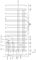
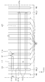
도 1은 본 발명의 몇몇 실시예들에 따른 반도체 장치를 설명하기 위한 레이아웃도이다.
도 2 내지 도 5는 각각 도 1의 A - A, B - B, C - C 및 D - D를 따라서 절단한 단면도이다.
도 6 내지 도 8은 각각 본 발명의 몇몇 실시예들에 따른 반도체 장치를 설명하기 위한 도면이다.
도 9a 및 도 9b는 각각 본 발명의 몇몇 실시예들에 따른 반도체 장치를 설명하기 위한 도면이다.
도 10은 본 발명의 몇몇 실시예들에 따른 반도체 장치를 설명하기 위한 레이아웃도이다.
도 11은 도 10의 A - A를 따라서 절단한 단면도이다.
도 12 내지 도 14는 각각 본 발명의 몇몇 실시예들에 따른 반도체 장치를 설명하기 위한 도면이다.
도 15 및 도 16은 각각 본 발명의 몇몇 실시예들에 따른 반도체 장치를 설명하기 위한 도면이다.
도 17은 본 발명의 몇몇 실시예들에 따른 반도체 장치를 설명하기 위한 레이아웃도이다.
도 18은 도 17의 E - E를 따라 절단한 단면도이다.
도 19는 본 발명의 몇몇 실시예들에 따른 반도체 장치를 설명하기 위한 도면이다.
도 20은 본 발명의 몇몇 실시예들에 따른 반도체 장치를 설명하기 위한 레이아웃도이다.
도 21은 도 20의 F - F를 따라 절단한 단면도이다.
도 22는 본 발명의 몇몇 실시예들에 따른 반도체 장치를 설명하기 위한 레이아웃도이다.
도 23은 본 발명의 몇몇 실시예들에 따른 반도체 장치를 설명하기 위한 레이아웃도이다.
도 24는 도 23의 F - F를 따라서 절단한 단면도이다.
도 25는 본 발명의 몇몇 실시예들에 따른 반도체 장치를 설명하기 위한 레이아웃도이다.
도 26은 도 25의 A - A를 따라서 절단한 단면도이다.
도 27은 본 발명의 몇몇 실시예들에 따른 반도체 장치를 설명하기 위한 평면도이다.
도 28 내지 도 35는 본 발명의 몇몇 실시예들에 따른 반도체 장치 제조 방법을 설명하기 위한 중간단계 도면들이다.1 is a layout diagram illustrating a semiconductor device according to some embodiments of the present invention.
2 to 5 are cross-sectional views taken along lines A - A, B - B, C - C and D - D of FIG. 1, respectively.
6 to 8 are diagrams for explaining a semiconductor device according to some embodiments of the present invention, respectively.
9A and 9B are diagrams for explaining a semiconductor device according to some embodiments of the present invention, respectively.
10 is a layout diagram illustrating a semiconductor device according to some embodiments of the present invention.
11 is a cross-sectional view taken along line A - A of FIG. 10 .
12 to 14 are diagrams for explaining a semiconductor device according to some embodiments of the present invention, respectively.
15 and 16 are diagrams for explaining a semiconductor device according to some embodiments of the present invention, respectively.
17 is a layout diagram illustrating a semiconductor device according to some embodiments of the present invention.
18 is a cross-sectional view taken along line E - E of FIG. 17 .
19 is a diagram for describing a semiconductor device according to some embodiments of the present invention.
20 is a layout diagram illustrating a semiconductor device according to some embodiments of the present invention.
21 is a cross-sectional view taken along line F - F of FIG. 20 .
22 is a layout diagram illustrating a semiconductor device according to some embodiments of the present invention.
23 is a layout diagram illustrating a semiconductor device according to some embodiments of the present invention.
24 is a cross-sectional view taken along line F - F of FIG. 23 .
25 is a layout diagram illustrating a semiconductor device according to some embodiments of the present invention.
26 is a cross-sectional view taken along line A - A of FIG. 25 .
27 is a plan view illustrating a semiconductor device according to some embodiments of the present invention.
28 to 35 are intermediate steps for explaining a method of manufacturing a semiconductor device according to some embodiments of the present invention.
도 1은 본 발명의 몇몇 실시예들에 따른 반도체 장치를 설명하기 위한 레이아웃도이다. 도 2 내지 도 5는 각각 도 1의 A - A, B - B, C - C 및 D - D를 따라서 절단한 단면도이다. 1 is a layout diagram illustrating a semiconductor device according to some embodiments of the present invention. 2 to 5 are cross-sectional views taken along lines A - A, B - B, C - C and D - D of FIG. 1, respectively.
도 1 내지 도 5를 참고하면, 본 발명의 몇몇 실시예들에 따른 반도체 장치는 제1 테이퍼진(tapered) 핀형 패턴(110)과, 제1 노말(normal) 핀형 패턴(210)과, 노말 게이트 전극(120)과, 종단(terminal) 게이트 전극(160_1, 160_2, 160_3)과, 더미 게이트 전극(140)을 포함할 수 있다. 1 to 5 , a semiconductor device according to some embodiments of the present invention includes a first tapered fin-
기판(100)은 예를 들어, 벌크 실리콘 또는 SOI(silicon-on-insulator)일 수 있다. 이와 달리, 기판(100)은 실리콘 기판일 수도 있고, 또는 다른 물질, 예를 들어, 실리콘게르마늄, SGOI(silicon germanium on insulator), 안티몬화 인듐, 납 텔루르 화합물, 인듐 비소, 인듐 인화물, 갈륨 비소 또는 안티몬화 갈륨을 포함할 수 있다. 또는, 기판(100)은 베이스 기판 상에 에피층이 형성된 것일 수도 있지만, 이에 제한되는 것은 아니다.The
제1 테이퍼진 핀형 패턴(110)은 액티브 영역(ACT) 내에 형성될 수 있다. 제1 테이퍼진 핀형 패턴(110)은 제1 방향(X)으로 연장되는 장변(112)과, 제2 방향(Y)으로 연장되는 단변(111a, 111b)을 포함할 수 있다. 제1 테이퍼진 핀형 패턴의 장변(112)은 제1 테이퍼진 핀형 패턴의 제1 단변(111a)과, 제1 테이퍼진 핀형 패턴의 제2 단변(111b)을 연결할 수 있다. 제1 테이퍼진 핀형 패턴의 제1 단변(111a)은 제1 테이퍼진 핀형 패턴의 제2 단변(111b)과 마주본다.The first tapered fin-
제1 노말 핀형 패턴(210)은 액티브 영역(ACT) 내에 형성될 수 있다. 액티브 영역(ACT) 내에, 제1 노말 핀형 패턴(210)은 적어도 하나 이상이 형성될 수 있다. 제1 노말 핀형 패턴(210)은 제1 방향(X)으로 연장되는 장변(212)과, 제2 방향(Y)으로 연장되는 단변(211a, 211b)을 포함할 수 있다. 제1 노말 핀형 패턴의 장변(212)은 제1 노말 핀형 패턴의 제1 단변(211a)과, 제1 노말 핀형 패턴의 제2 단변(211b)을 연결할 수 있다. 제1 노말 핀형 패턴의 제1 단변(211a)은 제1 노말 핀형 패턴의 제2 단변(211b)과 마주본다. The first
제1 노말 핀형 패턴(210)은 제1 테이퍼진 핀형 패턴(110)과 나란하게 배치될 수 있다. 예를 들어, 제1 노말 핀형 패턴의 장변(212)은 제1 테이퍼진 핀형 패턴의 장변(112)과 마주보고 있을 수 있다. 즉, 제1 테이퍼진 핀형 패턴(110)과 제1 노말 핀형 패턴(210)은 제2 방향(Y)으로 배열되어 있을 수 있다. The first normal fin-
제1 노말 핀형 패턴(210)은 제1 테이퍼진 핀형 패턴의 제1 단변(111a)보다 제1 방향(X)으로 돌출된 부분을 포함한다. 즉, 제2 방향(Y)에서 바라볼 때, 제1 노말 핀형 패턴(210)의 일부는 제1 테이퍼진 핀형 패턴(110)과 중첩되고, 제1 노말 핀형 패턴(210)의 나머지는 제1 테이퍼진 핀형 패턴(110)과 중첩되지 않는다. The first normal fin-
예를 들어, 제1 노말 핀형 패턴의 제2 단변(211b) 및 제1 테이퍼진 핀형 패턴의 제2 단변(111b)은 제2 방향(Y)으로 정렬되어 있을 수 있다. For example, the second
본 발명의 몇몇 실시예들에 따른 반도체 장치에서, 제1 노말 핀형 패턴(210)과, 제1 테이퍼진 핀형 패턴(110) 사이에, 추가적인 테이퍼진 핀형 패턴은 형성되지 않을 수 있다. In the semiconductor device according to some embodiments of the present invention, an additional tapered fin-shaped pattern may not be formed between the first normal fin-
제1 테이퍼진 핀형 패턴(110) 및 제1 노말 핀형 패턴(210)은 기판(100)의 일부일 수도 있고, 기판(100)으로부터 성장된 에피층(epitaxial layer)을 포함할 수 있다. 제1 테이퍼진 핀형 패턴(110) 및 제1 노말 핀형 패턴(210)은 서로 동일한 물질을 포함할 수 있다. 각각의 제1 테이퍼진 핀형 패턴(110) 및 제1 노말 핀형 패턴(210)은 예를 들어, 원소 반도체 물질인 실리콘 또는 게르마늄을 포함할 수 있다. 또한, 각각의 제1 테이퍼진 핀형 패턴(110) 및 제1 노말 핀형 패턴(210)은 화합물 반도체를 포함할 수 있고, 예를 들어, IV-IV족 화합물 반도체 또는 III-V족 화합물 반도체를 포함할 수 있다.The first tapered fin-
구체적으로, IV-IV족 화합물 반도체를 예로 들면, 각각의 제1 테이퍼진 핀형 패턴(110) 및 제1 노말 핀형 패턴(210)은 탄소(C), 규소(Si), 게르마늄(Ge), 주석(Sn) 중 적어도 2개 이상을 포함하는 이원계 화합물(binary compound), 삼원계 화합물(ternary compound) 또는 이들에 IV족 원소가 도핑된 화합물일 수 있다. Specifically, taking the group IV-IV compound semiconductor as an example, each of the first tapered fin-shaped
III-V족 화합물 반도체를 예로 들면, 각각의 제1 테이퍼진 핀형 패턴(110) 및 제1 노말 핀형 패턴(210)은 III족 원소로 알루미늄(Al), 갈륨(Ga) 및 인듐(In) 중 적어도 하나와 V족 원소인 인(P), 비소(As) 및 안티모늄(Sb) 중 하나가 결합되어 형성되는 이원계 화합물, 삼원계 화합물 또는 사원계 화합물 중 하나일 수 있다.Taking the group III-V compound semiconductor as an example, each of the first tapered fin-shaped
본 발명의 몇몇 실시예들에 따른 반도체 장치에서, 제1 테이퍼진 핀형 패턴(110) 및 제1 노말 핀형 패턴(210)은 실리콘을 포함하는 실리콘 핀형 패턴인 것으로 설명한다.In the semiconductor device according to some embodiments of the present invention, the first tapered fin-shaped
제1 테이퍼진 핀형 패턴(110) 및 제1 노말 핀형 패턴(210)이 형성되는 액티브 영역(ACT)은 제1 깊이(D1)의 깊은 트렌치(deep trench)(DT)에 의해 정의될 수 있다. The active region ACT in which the first tapered fin-shaped
제1 테이퍼진 핀형 패턴(110) 및 제1 노말 핀형 패턴(210)은 제3 깊이(D3)의 핀 트렌치(FT)에 의해 정의될 수 있다. 핀 트렌치(FT)의 깊이(D3)는 깊은 트렌치(DT)의 깊이(D1)보다 작다. 예를 들어, 제1 테이퍼진 핀형 패턴의 장변(112) 및 제1 노말 핀형 패턴의 장변(212)은 핀 트렌치(FT)에 의해 정의될 수 있다. 제1 테이퍼진 핀형 패턴의 장변(112)을 정의하는 제1 테이퍼진 핀형 패턴의 장측벽(112s)과, 제1 노말 핀형 패턴의 장변(212)을 정의하는 제1 노말 핀형 패턴의 장측벽(212s)은 핀 트렌치(FT)에 의해 정의될 수 있다.The first tapered fin-shaped
제1 테이퍼진 핀형 패턴의 제1 단측벽(111as)은 제1 테이퍼진 핀형 패턴의 제1 단변(111a)을 정의할 수 있다. 제1 테이퍼진 핀형 패턴의 제1 단측벽(111as)의 적어도 일부는 제2 깊이(D2)의 제1 얕은 트렌치(shallow trench)(ST1)에 의해 정의될 수 있다. 제1 테이퍼진 핀형 패턴의 제1 단측벽(111as)은 제1 얕은 트렌치(ST1)의 측벽을 포함할 수 있다.The first short side wall 111as of the first tapered fin-shaped pattern may define a first
제1 얕은 트렌치(ST1)의 깊이(D2)는 깊은 트렌치(DT)의 깊이(D1)보다 작다. 제1 얕은 트렌치(ST1)의 깊이(D2)는 핀 트렌치(FT)의 깊이(D3)와 동일하거나, 작을 수 있다. 예를 들어, 깊은 트렌치(DT)의 깊이(D1), 제1 얕은 트렌치(ST1)의 깊이(D2) 및 핀 트렌치(FT)의 깊이(D3)는 제1 테이퍼진 핀형 패턴(110)의 상면을 기준으로 정의될 수 있다.A depth D2 of the first shallow trench ST1 is smaller than a depth D1 of the deep trench DT. A depth D2 of the first shallow trench ST1 may be equal to or smaller than a depth D3 of the fin trench FT. For example, the depth D1 of the deep trench DT, the depth D2 of the first shallow trench ST1, and the depth D3 of the fin trench FT are the upper surface of the first tapered fin-shaped
도 2 및 도 5에서, 제1 얕은 트렌치(ST1)의 깊이(D2) 및 핀 트렌치(FT)의 깊이(D3)는 동일할 수 있다. 2 and 5 , the depth D2 of the first shallow trench ST1 and the depth D3 of the fin trench FT may be the same.
제1 테이퍼진 핀형 패턴의 제1 단측벽(111as)을 정의하는 제1 얕은 트렌치(ST1)는 깊은 트렌치(DT)와 바로 인접할 수 있다. 여기서, 바로 인접한다는 의미는, 깊은 트렌치(DT)와 제1 얕은 트렌치(ST1) 사이에, 다른 제2 깊이(D2)의 트렌치(즉, shallow trench)가 배치되지 않는다는 것을 의미이다. The first shallow trench ST1 defining the first short sidewall 111as of the first tapered fin-shaped pattern may be directly adjacent to the deep trench DT. Here, the immediate proximity means that a trench (ie, a shallow trench) of a second depth D2 is not disposed between the deep trench DT and the first shallow trench ST1 .
깊은 트렌치(DT)의 측벽과, 제1 얕은 트렌치(ST1)의 측벽은 서로 연결될 수 있다. 깊은 트렌치(DT)의 측벽과, 제1 얕은 트렌치(ST1)의 측벽 사이에, 제1 연결 부분(TCP1)이 배치될 수 있다. 깊은 트렌치(DT)의 측벽과, 제1 얕은 트렌치(ST1)의 측벽은 제1 연결 부분(TCP1)을 매개로 연결될 수 있다. 제1 연결 부분(TCP1)은 제1 테이퍼진 핀형 패턴의 제1 단측벽(111as)과, 깊은 트렌치(DT)의 측벽을 연결할 수 있다. The sidewall of the deep trench DT and the sidewall of the first shallow trench ST1 may be connected to each other. A first connection portion TCP1 may be disposed between the sidewall of the deep trench DT and the sidewall of the first shallow trench ST1 . The sidewall of the deep trench DT and the sidewall of the first shallow trench ST1 may be connected via the first connection portion TCP1 . The first connection portion TCP1 may connect the first short sidewall 111as of the first tapered fin-shaped pattern and the sidewall of the deep trench DT.
깊은 트렌치(DT)의 측벽과, 제1 얕은 트렌치(ST1)의 측벽이 연결되는 지점에, 제1 연결 부분(TCP1)이 형성될 수 있다. 제1 연결 부분(TCP1)은 제1 얕은 트렌치(ST1)에 의해 정의될 수 있다. 제1 연결 부분(TCP1)은 제1 얕은 트렌치(ST1)의 바닥면을 포함할 수 있다. 도 2 및 도 5에서, 제1 연결 부분(TCP1)의 깊이(D2) 및 핀 트렌치(FT)의 깊이(D3)는 동일할 수 있다.A first connection portion TCP1 may be formed at a point where the sidewall of the deep trench DT and the sidewall of the first shallow trench ST1 are connected. The first connection portion TCP1 may be defined by the first shallow trench ST1 . The first connection portion TCP1 may include a bottom surface of the first shallow trench ST1 . 2 and 5 , the depth D2 of the first connection portion TCP1 and the depth D3 of the fin trench FT may be the same.
예를 들어, 제1 연결 부분(TCP1)과 깊은 트렌치(DT)의 측벽이 연결되는 부분은 각진 형상을 가질 수 있다. 제1 얕은 트렌치(ST1)의 바닥면과 깊은 트렌치(DT)의 측벽이 연결되는 부분은 라운딩되어 있지 않을 수 있다. For example, a portion where the first connection portion TCP1 and the sidewall of the deep trench DT are connected may have an angular shape. A portion where the bottom surface of the first shallow trench ST1 and the sidewall of the deep trench DT are connected may not be rounded.
깊은 트렌치(DT)의 바닥면을 기준으로, 제1 연결 부분(TCP1)의 높이는 D1 - D2일 수 있다. 깊은 트렌치(DT)의 측벽과, 제1 얕은 트렌치(ST1)의 측벽이 연결되는 지점의 높이는 D1 - D2일 수 있다. Based on the bottom surface of the deep trench DT, the height of the first connection portion TCP1 may be D1 - D2. The height of the point where the sidewall of the deep trench DT and the sidewall of the first shallow trench ST1 are connected may be D1 - D2.
깊은 트렌치(DT)의 측벽의 기울기는 제1 얕은 트렌치(ST1)의 측벽의 기울기와 동일할 수도 있고, 서로 다를 수도 있다. The slope of the sidewall of the deep trench DT may be the same as or different from the slope of the sidewall of the first shallow trench ST1 .
제1 테이퍼진 핀형 패턴의 제2 단측벽(111bs)은 제1 테이퍼진 핀형 패턴의 제2 단변(111b)을 정의할 수 있다. 제1 테이퍼진 핀형 패턴의 제2 단측벽(111bs)은 깊은 트렌치(DT)에 의해 정의될 수 있다. 제1 테이퍼진 핀형 패턴의 제2 단측벽(111bs)은 깊은 트렌치(DT)의 측벽을 포함할 수 있다. The second short sidewall 111bs of the first tapered fin-shaped pattern may define a second
제1 노말 핀형 패턴의 제2 단변(211b)을 정의하는 제1 노말 핀형 패턴의 단측벽(211bs)은 깊은 트렌치(DT)에 의해 정의될 수 있다. 제1 노말 핀형 패턴의 단측벽(211bs)은 깊은 트렌치(DT)의 측벽을 포함할 수 있다. 도시되지 않았지만, 제1 노말 핀형 패턴의 제1 단변(211a)을 정의하는 제1 노말 핀형 패턴(210)의 단측벽도 깊은 트렌치(DT)에 의해 정의될 수 있다. The short sidewall 211bs of the first normal fin-shaped pattern defining the second
도 4 및 도 5에서, 제1 테이퍼진 핀형 패턴(110)이 위치할 영역에 깊은 트렌치(DT)가 형성될 수 있다.4 and 5 , a deep trench DT may be formed in a region where the first tapered fin-shaped
필드 절연막(105)은 기판(100) 상에 형성될 수 있다. 필드 절연막(105)은 깊은 트렌치(DT)의 일부, 제1 얕은 트렌치(ST1)의 일부 및 핀 트렌치(FT)의 일부를 채울 수 있다. 필드 절연막(105)은 제1 테이퍼진 핀형 패턴(110)의 일부 및 제1 노말 핀형 패턴(210)의 일부를 감쌀 수 있다. 필드 절연막(105)은 제1 테이퍼진 핀형 패턴의 장측벽(112s)의 일부, 제1 테이퍼진 핀형 패턴의 제1 단측벽(111as)의 일부, 제1 테이퍼진 핀형 패턴의 제2 단측벽(111bs)의 일부, 제1 노말 핀형 패턴의 장측벽(212s)의 일부 및 제1 노말 핀형 패턴의 단측벽(211bs)의 일부를 덮을 수 있다. The
제1 테이퍼진 핀형 패턴(110)의 상면과, 제1 노말 핀형 패턴(210)의 상면은 제1 테이퍼진 핀형 패턴의 장측벽(112s) 및 제1 노말 핀형 패턴의 장측벽(212s) 상에 형성된 필드 절연막(105)의 상면보다 위로 돌출되어 있을 수 있다. 제1 테이퍼진 핀형 패턴(110) 및 제1 노말 핀형 패턴(210)은 필드 절연막(105)에 의해 정의될 수 있다.The upper surface of the first tapered fin-shaped
제1 테이퍼진 핀형 패턴(110)의 상면을 기준으로, 필드 절연막(105)의 상면은 깊은 트렌치(DT)의 측벽과, 제1 얕은 트렌치(ST1)의 측벽이 연결되는 지점보다 높게 위치한다. 예를 들어, 제1 테이퍼진 핀형 패턴(110)의 상면으로부터 필드 절연막(105)의 상면까지의 거리는 제1 얕은 트렌치(ST1)의 깊이(D2)보다 작을 수 있다.Based on the top surface of the first tapered fin-shaped
제1 테이퍼진 핀형 패턴의 제1 단측벽(111as)에 포함된 제1 연결 부분(TCP1)은 필드 절연막(105)에 의해 덮여 있을 수 있다. The first connection portion TCP1 included in the first short sidewall 111as of the first tapered fin-shaped pattern may be covered by the
필드 절연막(105)은 예를 들어, 실리콘 산화물, 실리콘 질화물, 실리콘 산질화물, FOX(Flowable Oxide), TOSZ(Tonen SilaZene), USG(Undoped Silica Glass), BSG(Borosilica Glass), PSG(PhosphoSilica Glass), BPSG(BoroPhosphoSilica Glass), PETEOS(Plasma Enhanced Tetra Ethyl Ortho Silicate), FSG(Fluoride Silicate Glass), CDO(Carbon Doped silicon Oxide), Xerogel, Aerogel, Amorphous Fluorinated Carbon, OSG(Organo Silicate Glass), Parylene, BCB(bis-benzocyclobutenes), SiLK, polyimide, porous polymeric material 또는 이들의 조합을 포함할 수 있으나, 이에 제한되는 것은 아니다. The
필드 절연막(105)은 제1 테이퍼진 핀형 패턴(110) 및 필드 절연막(105) 사이와, 제1 노말 핀형 패턴(210) 및 필드 절연막(105)에 형성되는 적어도 하나 이상의 필드 라이너막을 더 포함할 수도 있다. 필드 절연막(105)이 필드 라이너막을 더 포함할 경우, 필드 라이너막은 폴리 실리콘, 비정질 실리콘, 실리콘 산질화물, 실리콘 질화물, 실리콘 산화물 중 적어도 하나를 포함할 수 있다.The
도 2 및 도 4에서, 깊은 트렌치(DT)의 일부를 채우는 필드 절연막(105)은 제1 얕은 트렌치(ST1)의 일부 및 핀 트렌치(FT)의 일부를 채우는 필드 절연막(105)과 동일한 물질인 것으로 도시하였지만, 이에 제한되는 것은 아니다. 즉, 깊은 트렌치(DT)의 일부를 채우는 필드 절연막(105)은 제1 얕은 트렌치(ST1)의 일부 및 핀 트렌치(FT)의 일부를 채우는 필드 절연막(105)과 다른 물질을 포함할 수 있다.2 and 4 , the
노말 게이트 전극(120)은 필드 절연막(105) 상에서 제2 방향(Y)으로 연장될 수 있다. 노말 게이트 전극(120)은 제1 테이퍼진 핀형 패턴(110) 및 제1 노말 핀형 패턴(210) 상에, 제1 테이퍼진 핀형 패턴(110) 및 제1 노말 핀형 패턴(210)과 교차하도록 형성될 수 있다. 또는, 노말 게이트 전극(120)은 제1 노말 핀형 패턴(210) 상에 제1 노말 핀형 패턴(210)과 교차하도록 형성될 수 있다. The
노말 게이트 전극(120)은 제1 테이퍼진 핀형 패턴의 장변(112) 및/또는 제1 노말 핀형 패턴의 장변(212)과 중첩될 수 있다. 노말 게이트 전극(120)은 제1 테이퍼진 핀형 패턴의 제1 단변(111a) 및 제2 단변(111b)과 중첩되지 않고, 제1 노말 핀형 패턴의 제1 단변(211a) 및 제2 단변(211b)과 중첩되지 않는다. The
종단 게이트 전극(160_1, 160_2, 160_3)은 필드 절연막(105) 상에서 제2 방향(Y)으로 연장될 수 있다. 제1 종단 게이트 전극(160_1) 및 제2 종단 게이트 전극(160_2)은 제1 테이퍼진 핀형 패턴(110) 및 제1 노말 핀형 패턴(210) 상에, 제1 테이퍼진 핀형 패턴(110) 및 제1 노말 핀형 패턴(210)과 교차하도록 형성될 수 있다. 제3 종단 게이트 전극(160_3)은 제1 노말 핀형 패턴(210) 상에 제1 노말 핀형 패턴(210)과 교차하도록 형성될 수 있다. The termination gate electrodes 160_1 , 160_2 , and 160_3 may extend in the second direction Y on the
제1 종단 게이트 전극(160_1)은 제1 테이퍼진 핀형 패턴의 제1 단변(111a)을 포함하는 제1 테이퍼진 핀형 패턴(110)의 제1 종단과 중첩될 수 있다. 제2 종단 게이트 전극(160_2)은 제1 테이퍼진 핀형 패턴의 제2 단변(111b)을 포함하는 제1 테이퍼진 핀형 패턴(110)의 제2 종단과 중첩될 수 있다. 제1 노말 핀형 패턴의 제2 단변(211b) 및 제1 테이퍼진 핀형 패턴의 제2 단변(111b)이 제2 방향(Y)으로 정렬되어 있을 때, 제2 종단 게이트 전극(160_2)은 제1 노말 핀형 패턴의 제2 단변(211b)을 포함하는 제1 노말 핀형 패턴(210)의 제2 종단과 중첩될 수 있다. 제3 종단 게이트 전극(160_3)은 제1 노말 핀형 패턴의 제1 단변(211a)을 포함하는 제1 노말 핀형 패턴(210)의 제1 종단과 중첩될 수 있다. The first termination gate electrode 160_1 may overlap the first termination of the first tapered fin-shaped
도 2 및 도 3에서, 제1 종단 게이트 전극(160_1)은 제1 테이퍼진 핀형 패턴(110)의 제1 종단을 감싸고, 제2 종단 게이트 전극(160_2)은 제1 테이퍼진 핀형 패턴(110)의 제2 종단 및 제1 노말 핀형 패턴(210)의 제2 종단을 감싸고, 제3 종단 게이트 전극(160_3)은 제1 노말 핀형 패턴(210)의 제1 종단을 감싸는 것으로 도시되었지만, 설명의 편의를 위한 것일 뿐, 이에 제한되는 것은 아니다. 즉, 종단 게이트 전극(160_1, 160_2, 160_3)의 적어도 일부는 제1 테이퍼진 핀형 패턴(110)의 상면 및/또는 제1 노말 핀형 패턴(210)의 상면과 중첩되면 충분하다. 2 and 3 , the first termination gate electrode 160_1 surrounds the first end of the first tapered fin-shaped
평면도에서, 제1 종단 게이트 전극(160_1)은 제1 얕은 트렌치(ST1)의 측벽 및 깊은 트렌치(DT)의 측벽이 연결되는 지점과 중첩될 수 있다. 예를 들어, 평면도에서, 제1 종단 게이트 전극(160_1)은 제1 연결 부분(TCP1)의 적어도 일부와 중첩될 수 있다. 평면도에서, 제1 종단 게이트 전극(160_1)은 제1 연결 부분(TCP1) 전체와 중첩되고, 깊은 트렌치(DT)의 측벽의 적어도 일부와 중첩될 수도 있다. In a plan view, the first termination gate electrode 160_1 may overlap a point where the sidewall of the first shallow trench ST1 and the sidewall of the deep trench DT are connected. For example, in a plan view, the first termination gate electrode 160_1 may overlap at least a portion of the first connection portion TCP1 . In a plan view, the first termination gate electrode 160_1 may overlap the entire first connection portion TCP1 and at least a portion of the sidewall of the deep trench DT.
제1 종단 게이트 전극(160_1) 및 제2 종단 게이트 전극(160_2) 사이에 하나의 노말 게이트 전극(120)이 형성되고, 제1 종단 게이트 전극(160_1) 및 제3 종단 게이트 전극(160_3) 사이에 8개의 노말 게이트 전극(120)이 형성되는 것으로 도시하였지만, 이에 제한되는 것은 아니다. 인접하는 종단 게이트 전극 사이에, 노말 게이트 전극이 배치되지 않을 수도 있음은 물론이다. One
더미 게이트 전극(140)은 필드 절연막(105) 상에서 제2 방향(Y)으로 연장될 수 있다. 더미 게이트 전극(140)은 제1 테이퍼진 핀형 패턴(110) 및 제1 노말 핀형 패턴(210)과 교차하지 않을 수 있다. The
노말 게이트 전극(120) 및 종단 게이트 전극(160_1, 160_2, 160_3)은 더미 게이트 전극(140) 사이에 배치될 수 있다. 제1 테이퍼진 핀형 패턴(110) 및 제1 노말 핀형 패턴(210)은 더미 게이트 전극(140) 사이에 배치될 수 있다. The
노말 게이트 전극(120), 종단 게이트 전극(160_1, 160_2, 160_3) 및 더미 게이트 전극(140)은 각각 예를 들어, 티타늄 질화물(TiN), 탄탈륨 탄화물(TaC), 탄탈륨 질화물(TaN), 티타늄 실리콘 질화물(TiSiN), 탄탈륨 실리콘 질화물(TaSiN), 탄탈륨 티타늄 질화물(TaTiN), 티타늄 알루미늄 질화물(TiAlN), 탄탈륨 알루미늄 질화물(TaAlN), 텅스텐 질화물(WN), 루테늄(Ru), 티타늄 알루미늄(TiAl), 티타늄 알루미늄 탄질화물(TiAlC-N), 티타늄 알루미늄 탄화물(TiAlC), 티타늄 탄화물(TiC), 탄탈륨 탄질화물(TaCN), 텅스텐(W), 알루미늄(Al), 구리(Cu), 코발트(Co), 티타늄(Ti), 탄탈륨(Ta), 니켈(Ni), 백금(Pt), 니켈 백금(Ni-Pt), 니오븀(Nb), 니오븀 질화물(NbN), 니오븀 탄화물(NbC), 몰리브덴(Mo), 몰리브덴 질화물(MoN), 몰리브덴 탄화물(MoC), 텅스텐 탄화물(WC), 로듐(Rh), 팔라듐(Pd), 이리듐(Ir), 오스뮴(Os), 은(Ag), 금(Au), 아연(Zn), 바나듐(V) 및 이들의 조합 중 적어도 하나를 포함할 수 있다. The
노말 게이트 전극(120), 종단 게이트 전극(160_1, 160_2, 160_3) 및 더미 게이트 전극(140)은 예를 들어, 리플레이스먼트 공정(replacement process)(또는 게이트 라스트 공정(gate last process))을 통해서 형성될 수 있으나, 이에 한정되는 것은 아니다. The
노말 스페이서(135)는 노말 게이트 전극(120)의 측벽 상에 형성될 수 있다. 노말 스페이서(135)는 노말 게이트 트렌치(135t)를 정의할 수 있다. 노말 게이트 전극(120)은 노말 게이트 트렌치(135t) 내에 형성된다. 종단 스페이서(175)는 종단 게이트 전극(160_1, 160_2, 160_3)의 측벽 상에 형성될 수 있다. 종단 스페이서(175)는 종단 게이트 트렌치(175t)를 정의할 수 있다. 각각의 종단 게이트 전극(160_1, 160_2, 160_3)은 종단 게이트 트렌치(175t) 내에 형성된다. 더미 스페이서(145)는 더미 게이트 전극(140)의 측벽 상에 형성될 수 있다. 더미 스페이서(145)는 더미 게이트 트렌치(145t)를 정의할 수 있다. 더미 게이트 전극(140)은 더미 게이트 트렌치(145t) 내에 형성된다. 각각의 노말 스페이서(135), 더미 스페이서(145) 및 종단 스페이서(175)는 예를 들어, 실리콘 질화물(SiN), 실리콘 산질화물(SiON), 실리콘 산화물(SiO2), 및 실리콘 산탄질화물(SiOCN) 중 적어도 하나를 포함할 수 있다.The
경우에 따라, 평면도에서, 종단 스페이서(175)는 제1 연결 부분(TCP1)의 일부와 중첩될 수 있다. 또는, 종단 스페이서(175)는 깊은 트렌치(DT)의 측벽의 적어도 일부와 중첩될 수도 있다.In some cases, in a plan view, the
노말 게이트 절연막(130) 및 종단 게이트 절연막(170)은 제1 테이퍼진 핀형 패턴(110)과, 제1 노말 핀형 패턴(210)과, 필드 절연막(105) 상에 형성될 수 있다. 노말 게이트 절연막(130)은 노말 게이트 트렌치(135t)의 측벽 및 바닥면을 따라 형성될 수 있다. 종단 게이트 절연막(170)은 종단 게이트 트렌치(175t)의 측벽 및 바닥면을 따라 형성될 수 있다. 노말 게이트 절연막(130) 및 종단 게이트 절연막(170)은 각각 필드 절연막(105)보다 위로 돌출된 제1 테이퍼진 핀형 패턴(110)의 프로파일 및/또는 제1 노말 핀형 패턴(210)의 프로파일을 따라 형성될 수 있다. 노말 게이트 전극(120)은 노말 게이트 절연막(130) 상에 형성되고, 종단 게이트 전극(160_1, 160_2, 160_3)은 종단 게이트 절연막(170) 상에 형성될 수 있다. 더미 게이트 절연막(142)은 필드 절연막(105)의 상면을 따라 형성될 수 있다. 더미 게이트 절연막(142)은 더미 게이트 트렌치(145t)의 측벽 및 바닥면을 따라 형성될 수 있다.The normal
도 2 및 도 3에서 도시한 것과 달리, 노말 게이트 절연막(130) 및 제1 테이퍼진 핀형 패턴(110) 사이와, 노말 게이트 절연막(130) 및 제1 노말 핀형 패턴(210) 사이와, 종단 게이트 절연막(170) 및 제1 테이퍼진 핀형 패턴(110) 사이와, 종단 게이트 절연막(170) 및 제1 노말 핀형 패턴(210) 사이에, 계면막(interfacial layer)이 더 형성될 수 있다. 제1 테이퍼진 핀형 패턴(110) 및 제1 노말 핀형 패턴(210)이 실리콘 핀형 패턴일 경우, 계면막은 예를 들어, 실리콘 산화물을 포함할 수 있다. 2 and 3 , between the normal
노말 게이트 절연막(130), 더미 게이트 절연막(142) 및 종단 게이트 절연막(170)은 실리콘 산화막보다 높은 유전 상수를 갖는 고유전체 물질을 포함할 수 있다. 예를 들어, 고유전체 물질은 하프늄 산화물(hafnium oxide), 하프늄 실리콘 산화물(hafnium silicon oxide), 하프늄 알루미늄 산화물(hafnium aluminum oxide), 란타늄 산화물(lanthanum oxide), 란타늄 알루미늄 산화물(lanthanum aluminum oxide), 지르코늄 산화물(zirconium oxide), 지르코늄 실리콘 산화물(zirconium silicon oxide), 탄탈륨 산화물(tantalum oxide), 티타늄 산화물(titanium oxide), 바륨 스트론튬 티타늄 산화물(barium strontium titanium oxide), 바륨 티타늄 산화물(barium titanium oxide), 스트론튬 티타늄 산화물(strontium titanium oxide), 이트륨 산화물(yttrium oxide), 알루미늄 산화물(aluminum oxide), 납 스칸듐 탄탈륨 산화물(lead scandium tantalum oxide), 또는 납 아연 니오브산염(lead zinc niobate) 중에서 하나 이상을 포함할 수 있다.The normal
제1 에피택셜 패턴(150)은 노말 게이트 전극(120)과 종단 게이트 전극(160_1, 160_2) 사이 또는 노말 게이트 전극(120) 사이에 형성될 수 있다. 제1 에피택셜 패턴(150)은 제1 테이퍼진 핀형 패턴(110) 상에 형성될 수 있다. 제2 에피택셜 패턴(250)은 노말 게이트 전극(120)과 종단 게이트 전극(160_1, 160_2) 사이 또는, 노말 게이트 전극(120) 사이에 형성될 수 있다. 제2 에피택셜 패턴(250)은 제1 노말 핀형 패턴(210) 상에 형성될 수 있다. 제1 에피택셜 패턴(150)은 제1 테이퍼진 핀형 패턴(110)을 채널 영역으로 사용하는 트랜지스터의 소오스/드레인에 포함되고, 제2 에피택셜 패턴(250)은 제1 노말 핀형 패턴(210)을 채널 영역으로 사용하는 트랜지스터의 소오스/드레인에 포함될 수 있다. 도 4에서, 인접하는 제1 노말 핀형 패턴(210) 상에 형성된 제2 에피택셜 패턴(250)은 서로 간에 접촉하는 것으로 도시하였지만, 이에 제한되는 것은 아니다. The first
층간 절연막(190)은 하부 층간 절연막(191)과 상부 층간 절연막(192)을 포함할 수 있다. 하부 층간 절연막(191)은 제1 에피택셜 패턴(150) 및 제2 에피택셜 패턴(250)을 덮을 수 있다. 예를 들어, 하부 층간 절연막(191)의 상면은 노말 게이트 전극(120)의 상면, 더미 게이트 전극(140)의 상면 및 종단 게이트 전극(160_1, 160_2, 160_3)의 상면과 코플래너(coplanar)할 수 있다. 상부 층간 절연막(192)은 하부 층간 절연막(191) 상에 형성된다. 상부 층간 절연막(192)는 노말 게이트 전극(120)의 상면, 더미 게이트 전극(140)의 상면 및 종단 게이트 전극(160_1, 160_2, 160_3) 상에 형성된다. The interlayer insulating
하부 층간 절연막(191) 및 상부 층간 절연막(192)은 각각 예를 들어, 실리콘 산화물, 실리콘 질화물, 실리콘 산질화물, FOX(Flowable Oxide), TOSZ(Tonen SilaZene), USG(Undoped Silica Glass), BSG(Borosilica Glass), PSG(PhosphoSilica Glass), BPSG(BoroPhosphoSilica Glass), PETEOS(Plasma Enhanced Tetra Ethyl Ortho Silicate), FSG(Fluoride Silicate Glass), CDO(Carbon Doped silicon Oxide), Xerogel, Aerogel, Amorphous Fluorinated Carbon, OSG(Organo Silicate Glass), Parylene, BCB(bis-benzocyclobutenes), SiLK, polyimide, porous polymeric material 또는 이들의 조합을 포함할 수 있으나, 이에 제한되는 것은 아니다.The lower
도 6 내지 도 8은 각각 본 발명의 몇몇 실시예들에 따른 반도체 장치를 설명하기 위한 도면이다. 설명의 편의상, 도 1 내지 도 5를 이용하여 설명한 것과 다른 점을 중심으로 설명한다.6 to 8 are diagrams for explaining a semiconductor device according to some embodiments of the present invention, respectively. For convenience of description, points different from those described with reference to FIGS. 1 to 5 will be mainly described.
도 6을 참고하면, 본 발명의 몇몇 실시예들에 따른 반도체 장치에서, 제1 테이퍼진 핀형 패턴의 제1 단측벽(111as)의 제1 연결 부분(TCP1)은 라운딩되어 있을 수 있다.Referring to FIG. 6 , in the semiconductor device according to some embodiments of the present disclosure, the first connection portion TCP1 of the first short side wall 111as of the first tapered fin-shaped pattern may be rounded.
즉, 제1 연결 부분(TCP1)과 깊은 트렌치(DT)의 측벽이 연결되는 부분은 라운딩된 형상을 가질 수 있다. 제1 얕은 트렌치(ST1)의 바닥면과 깊은 트렌치(DT)의 측벽이 연결되는 부분은 라운딩되어 있을 수 있다.That is, the portion where the first connection portion TCP1 and the sidewall of the deep trench DT are connected may have a rounded shape. A portion where the bottom surface of the first shallow trench ST1 and the sidewall of the deep trench DT are connected may be rounded.
도 7 및 도 8을 참고하면, 본 발명의 몇몇 실시예들에 따른 반도체 장치에서, 깊은 트렌치(DT)의 측벽은 제1 얕은 트렌치(ST1)의 측벽과 직접 연결될 수 있다. 7 and 8 , in the semiconductor device according to some embodiments of the present disclosure, the sidewall of the deep trench DT may be directly connected to the sidewall of the first shallow trench ST1 .
서로 직접 연결된 깊은 트렌치(DT)의 측벽의 기울기(α1)와 제1 얕은 트렌치(ST1)의 측벽의 기울기(α2)는 서로 다르다. The slope α1 of the sidewall of the deep trench DT directly connected to each other and the slope α2 of the sidewall of the first shallow trench ST1 are different from each other.
깊은 트렌치(DT)의 측벽과 제1 얕은 트렌치(ST1)의 측벽 사이에, 제1 연결 부분(TCP1)은 형성되지 않는다. 깊은 트렌치(DT)의 측벽과 제1 얕은 트렌치(ST1)의 측벽 사이에 제1 연결 부분(TCP1)이 형성되지 않지만, 제1 테이퍼진 핀형 패턴(110)의 상면을 기준으로, 필드 절연막(105)의 상면은 깊은 트렌치(DT)의 측벽과, 제1 얕은 트렌치(ST1)의 측벽이 연결되는 지점보다 높게 위치한다. The first connection portion TCP1 is not formed between the sidewall of the deep trench DT and the sidewall of the first shallow trench ST1 . Although the first connection portion TCP1 is not formed between the sidewall of the deep trench DT and the sidewall of the first shallow trench ST1 , the
도 5, 도 7 및 도 8에서, 제1 테이퍼진 핀형 패턴(110)의 상면을 기준으로, 깊은 트렌치(DT)의 측벽과 제1 얕은 트렌치(ST1)의 측벽이 직접 만나는 지점의 깊이는 핀 트렌치(FT)의 바닥면의 깊이(D3)보다 작을 수 있지만, 이에 제한되는 것은 아니다. 5, 7 and 8 , based on the upper surface of the first tapered fin-shaped
깊은 트렌치(DT)의 측벽과 제1 얕은 트렌치(ST1)의 측벽이 직접 만나는 지점이 핀 트렌치(FT)의 바닥면보다 높을 경우, 제1 테이퍼진 핀형 패턴의 제1 단측벽(111as)은 깊은 트렌치(DT)의 측벽의 일부와, 제1 얕은 트렌치(ST1)의 측벽을 포함할 수 있다.When the point where the sidewall of the deep trench DT and the sidewall of the first shallow trench ST1 directly meet is higher than the bottom surface of the fin trench FT, the first short sidewall 111as of the first tapered fin-shaped pattern is a deep trench A portion of the sidewall of the DT and the sidewall of the first shallow trench ST1 may be included.
도 7에서, 깊은 트렌치(DT)의 측벽의 기울기(α1)는 제1 얕은 트렌치(ST1)의 측벽의 기울기(α2)보다 크다. 도 8에서, 깊은 트렌치(DT)의 측벽의 기울기(α1)는 제1 얕은 트렌치(ST1)의 측벽의 기울기(α2)보다 작다. In FIG. 7 , the slope α1 of the sidewall of the deep trench DT is greater than the slope α2 of the sidewall of the first shallow trench ST1 . In FIG. 8 , the slope α1 of the sidewall of the deep trench DT is smaller than the slope α2 of the sidewall of the first shallow trench ST1 .
도 9a 및 도 9b는 각각 본 발명의 몇몇 실시예들에 따른 반도체 장치를 설명하기 위한 도면이다. 설명의 편의상, 도 1 내지 도 5를 이용하여 설명한 것과 다른 점을 중심으로 설명한다.9A and 9B are diagrams for explaining a semiconductor device according to some embodiments of the present invention, respectively. For convenience of description, points different from those described with reference to FIGS. 1 to 5 will be mainly described.
도 9a를 참고하면, 본 발명의 몇몇 실시예들에 따른 반도체 장치에서, 제1 테이퍼진 핀형 패턴의 제2 단변(111b)을 정의하는 제1 테이퍼진 핀형 패턴의 제2 단측벽(111bs)의 적어도 일부는 제4 깊이(D4)의 제2 얕은 트렌치(ST2)에 의해 정의될 수 있다. 제1 테이퍼진 핀형 패턴의 제2 단측벽(111bs)은 제2 얕은 트렌치(ST2)의 측벽을 포함할 수 있다. 제1 테이퍼진 핀형 패턴의 제2 단측벽(111bs)을 정의하는 제2 얕은 트렌치(ST2)는 깊은 트렌치(DT)와 바로 인접할 수 있다.Referring to FIG. 9A , in the semiconductor device according to some embodiments of the present invention, the second short side wall 111bs of the first tapered fin-shaped pattern defining the second
제2 얕은 트렌치(ST2)의 깊이(D4)는 깊은 트렌치(DT)의 깊이(D1)보다 작다. 제2 얕은 트렌치(ST2)의 깊이(D4)는 제1 테이퍼진 핀형 패턴(110)의 상면을 기준으로 정의될 수 있다. A depth D4 of the second shallow trench ST2 is smaller than a depth D1 of the deep trench DT. The depth D4 of the second shallow trench ST2 may be defined based on the upper surface of the first tapered fin-shaped
제조 공정 중, 제2 얕은 트렌치(ST2)는 제1 얕은 트렌치(ST1)와 동시에 형성될 수 있다. 제2 얕은 트렌치(ST2)의 깊이(D4)는 제1 얕은 트렌치(ST1)의 깊이(D2)와 실질적으로 동일할 수 있다. During the manufacturing process, the second shallow trench ST2 may be formed simultaneously with the first shallow trench ST1 . A depth D4 of the second shallow trench ST2 may be substantially equal to a depth D2 of the first shallow trench ST1 .
깊은 트렌치(DT)의 측벽과, 제2 얕은 트렌치(ST2)의 측벽은 서로 연결될 수 있다. 깊은 트렌치(DT)의 측벽과, 제2 얕은 트렌치(ST2)의 측벽 사이에, 제2 연결 부분(TCP2)이 배치될 수 있다. 깊은 트렌치(DT)의 측벽과, 제2 얕은 트렌치(ST2)의 측벽은 제2 연결 부분(TCP2)을 매개로 연결될 수 있다. The sidewall of the deep trench DT and the sidewall of the second shallow trench ST2 may be connected to each other. A second connection portion TCP2 may be disposed between the sidewall of the deep trench DT and the sidewall of the second shallow trench ST2 . The sidewall of the deep trench DT and the sidewall of the second shallow trench ST2 may be connected via the second connection portion TCP2 .
제2 연결 부분(TCP2)은 제1 테이퍼진 핀형 패턴의 제2 단측벽(111bs)과, 깊은 트렌치(DT)의 측벽을 연결할 수 있다. 깊은 트렌치(DT)의 측벽과, 제2 얕은 트렌치(ST2)의 측벽이 연결되는 지점에, 제2 연결 부분(TCP2)이 형성될 수 있다. 제2 연결 부분(TCP2)은 제2 얕은 트렌치(ST2)의 바닥면을 포함할 수 있다.The second connection portion TCP2 may connect the second short sidewall 111bs of the first tapered fin-shaped pattern and the sidewall of the deep trench DT. A second connection portion TCP2 may be formed at a point where the sidewall of the deep trench DT and the sidewall of the second shallow trench ST2 are connected. The second connection portion TCP2 may include a bottom surface of the second shallow trench ST2 .
제1 방향(X)으로 제2 연결 부분(TCP2)의 폭은 제1 방향(X)으로 제1 연결 부분(TCP1)의 폭과 다를 수 있지만, 이에 제한되는 것은 아니다. 제2 연결 부분(TCP2)의 폭이 제1 연결 부분(TCP1)의 폭과 다를 때, 제1 방향(X)으로 제2 연결 부분(TCP2)의 폭은 제1 방향(X)으로 제1 연결 부분(TCP1)의 폭보다 클 수 있다. The width of the second connection portion TCP2 in the first direction X may be different from the width of the first connection portion TCP1 in the first direction X, but is not limited thereto. When the width of the second connection part TCP2 is different from the width of the first connection part TCP1 , the width of the second connection part TCP2 in the first direction X is the first connection part in the first direction X It may be larger than the width of the portion TCP1 .
평면도에서, 제2 종단 게이트 전극(160_2)은 제2 얕은 트렌치(ST2)의 측벽과 중첩될 수 있다. 평면도에서, 제2 종단 게이트 전극(160_2)은 제2 연결 부분(TCP2)의 일부와 중첩될 수 있다. In a plan view, the second termination gate electrode 160_2 may overlap a sidewall of the second shallow trench ST2 . In a plan view, the second termination gate electrode 160_2 may overlap a portion of the second connection portion TCP2 .
평면도에서, 제2 종단 게이트 전극(160_2)은 깊은 트렌치(DT)의 측벽과 중첩되지 않는다. 평면도에서, 깊은 트렌치(DT)의 측벽의 적어도 일부는 제1 테이퍼진 핀형 패턴의 제2 단변(111b)에 인접하는 더미 게이트 전극(140)과 중첩될 수 있다.In the plan view, the second termination gate electrode 160_2 does not overlap the sidewall of the deep trench DT. In a plan view, at least a portion of a sidewall of the deep trench DT may overlap the
도 9a에서, 깊은 트렌치(DT)의 측벽과, 제2 얕은 트렌치(ST2)의 측벽을 연결하는 제2 연결 부분(TCP2)이 형성되는 것으로 도시하였지만, 이에 제한되는 것은 아니다. 즉, 깊은 트렌치(DT)의 측벽과, 제2 얕은 트렌치(ST2)의 측벽이 직접 연결되어 형성될 수도 있다. Although it is illustrated in FIG. 9A that the second connection portion TCP2 connecting the sidewall of the deep trench DT and the sidewall of the second shallow trench ST2 is formed, the present invention is not limited thereto. That is, the sidewall of the deep trench DT and the sidewall of the second shallow trench ST2 may be directly connected to each other.
도시하지 않았지만, 제1 노말 핀형 패턴의 제2 단변(211b)을 정의하는 제1 노말 핀형 패턴의 단측벽도 제4 깊이(D4)의 제2 얕은 트렌치(ST2)에 의해 정의될 수 있다.Although not illustrated, a short sidewall of the first normal fin-shaped pattern defining the second
제1 테이퍼진 핀형 패턴(110)의 상면을 기준으로, 필드 절연막(105)의 상면은 깊은 트렌치(DT)의 측벽과, 제2 얕은 트렌치(ST2)의 측벽이 연결되는 지점보다 높게 위치한다. 제1 테이퍼진 핀형 패턴(110)의 상면으로부터 필드 절연막(105)의 상면까지의 거리는 제2 얕은 트렌치(ST2)의 깊이(D4)보다 작을 수 있다.Based on the top surface of the first tapered fin-shaped
도 9b를 참고하면, 본 발명의 몇몇 실시예들에 따른 반도체 장치에서, 제1 얕은 트렌치(ST1)의 깊이(D2)는 핀 트렌치(FT)의 깊이(도 5의 D3)보다 작을 수 있다. Referring to FIG. 9B , in the semiconductor device according to some embodiments of the present disclosure, a depth D2 of the first shallow trench ST1 may be smaller than a depth D3 of the fin trench FT (D3 of FIG. 5 ).
제1 테이퍼진 핀형 패턴의 제1 단측벽(111as)은 깊은 트렌치(DT)의 측벽과, 제1 얕은 트렌치(ST1)의 측벽을 포함할 수 있다. 제1 테이퍼진 핀형 패턴의 제1 단측벽(111as)은 깊은 트렌치(DT)의 측벽과, 제1 얕은 트렌치(ST1)의 측벽이 연결되어 형성될 수 있다. The first short sidewall 111as of the first tapered fin-shaped pattern may include a sidewall of the deep trench DT and a sidewall of the first shallow trench ST1 . The first short sidewall 111as of the first tapered fin-shaped pattern may be formed by connecting the sidewall of the deep trench DT and the sidewall of the first shallow trench ST1 .
깊은 트렌치(DT)의 측벽과, 제1 얕은 트렌치(ST1)의 측벽이 연결되는 지점인 제1 연결 부분(TCP1)의 깊이(D2)는 핀 트렌치(FT)의 깊이(D3) 및 깊은 트렌치(DT)의 깊이(D1)보다 작을 수 있다.The depth D2 of the first connection portion TCP1, which is a point where the sidewall of the deep trench DT and the sidewall of the first shallow trench ST1 are connected, is the depth D3 of the fin trench FT and the depth of the deep trench ST1. It may be smaller than the depth D1 of DT).
도 10은 본 발명의 몇몇 실시예들에 따른 반도체 장치를 설명하기 위한 레이아웃도이다. 도 11은 도 10의 A - A를 따라서 절단한 단면도이다. 설명의 편의상, 도 1 내지 도 5를 이용하여 설명한 것과 다른 점을 중심으로 설명한다. 10 is a layout diagram illustrating a semiconductor device according to some embodiments of the present invention. 11 is a cross-sectional view taken along line A - A of FIG. 10 . For convenience of description, points different from those described with reference to FIGS. 1 to 5 will be mainly described.
도 10 및 도 11을 참고하면, 본 발명의 몇몇 실시예들에 따른 반도체 장치에서, 제2 방향(Y)으로 정렬된 제1 테이퍼진 핀형 패턴의 제2 단변(111b) 및 제1 노말 핀형 패턴의 제2 단변(211b)을 따라 깊은 트렌치(DT)가 형성되지 않을 수 있다.10 and 11 , in the semiconductor device according to some embodiments of the present invention, the second
제1 테이퍼진 핀형 패턴의 제2 단변(111b)을 정의하는 제1 테이퍼진 핀형 패턴의 제2 단측벽(111bs)은 제4 깊이(D4)의 제2 얕은 트렌치(ST2)에 의해 정의될 수 있다. 제1 테이퍼진 핀형 패턴의 제2 단측벽(111bs)은 제2 얕은 트렌치(ST2)의 측벽을 포함할 수 있다. 제1 노말 핀형 패턴의 제2 단변(211b)을 정의하는 제1 노말 핀형 패턴의 단측벽(211bs)은 제2 얕은 트렌치(ST2)에 의해 정의될 수 있다. 제1 노말 핀형 패턴의 단측벽(211bs)은 제2 얕은 트렌치(ST2)의 측벽을 포함할 수 있다.The second short sidewall 111bs of the first tapered fin-shaped pattern defining the second
제2 얕은 트렌치(ST2)의 깊이(D4)는 깊은 트렌치(DT)의 깊이(D1)보다 작다. 제조 공정 중, 제2 얕은 트렌치(ST2)는 제1 얕은 트렌치(ST1)와 동시에 형성될 수 있다. 제2 얕은 트렌치(ST2)의 깊이(D4)는 제1 얕은 트렌치(ST1)의 깊이(D2)와 실질적으로 동일할 수 있다. A depth D4 of the second shallow trench ST2 is smaller than a depth D1 of the deep trench DT. During the manufacturing process, the second shallow trench ST2 may be formed simultaneously with the first shallow trench ST1 . A depth D4 of the second shallow trench ST2 may be substantially equal to a depth D2 of the first shallow trench ST1 .
도 12 내지 도 14는 각각 본 발명의 몇몇 실시예들에 따른 반도체 장치를 설명하기 위한 도면이다. 설명의 편의상, 도 1 내지 도 5를 이용하여 설명한 것과 다른 점을 중심으로 설명한다.12 to 14 are diagrams for explaining a semiconductor device according to some embodiments of the present invention, respectively. For convenience of description, points different from those described with reference to FIGS. 1 to 5 will be mainly described.
도 12를 참고하면, 본 발명의 몇몇 실시예들에 따른 반도체 장치는 노말 게이트 캡핑 패턴(121)과, 더미 게이트 캡핑 패턴(141)과, 종단 게이트 캡핑 패턴(161)을 더 포함할 수 있다.Referring to FIG. 12 , the semiconductor device according to some exemplary embodiments may further include a normal
노말 게이트 전극(120)은 노말 게이트 트렌치(135t)의 일부를 채울 수 있다. 노말 게이트 캡핑 패턴(121)은 노말 게이트 전극(120) 상에 형성될 수 있다. 노말 게이트 캡핑 패턴(121)은 노말 게이트 트렌치(135t)의 나머지를 채울 수 있다. 종단 게이트 전극(160_1, 160_2)은 종단 게이트 트렌치(175t)의 일부를 채울 수 있다. 종단 게이트 캡핑 패턴(161)은 종단 게이트 전극(160_1, 160_2) 상에 형성될 수 있다. 종단 게이트 캡핑 패턴(161)은 종단 게이트 트렌치(175t)의 나머지를 채울 수 있다. 더미 게이트 캡핑 패턴(141)은 더미 게이트 트렌치(145t)의 일부를 채울 수 있다.The
노말 게이트 절연막(130)은 노말 스페이서(135) 및 노말 게이트 캡핑 패턴(121) 사이에 형성되지 않고, 종단 게이트 절연막(170)은 종단 스페이서(175) 및 종단 게이트 캡핑 패턴(161) 사이에 형성되지 않는 것으로 도시하였지만, 설명의 편의성을 위한 것일 뿐, 이에 제한되는 것은 아니다. The normal
노말 게이트 캡핑 패턴(121)의 상면과, 종단 게이트 캡핑 패턴(161)의 상면과, 더미 게이트 캡핑 패턴(141)의 상면은 각각 하부 층간 절연막(191)의 상면과 동일 평면에 놓일 수 있다. 노말 게이트 캡핑 패턴(121)과 종단 게이트 캡핑 패턴(161)과, 더미 게이트 캡핑 패턴(141)은 예를 들어, 하부 층간 절연막(191)에 대한 식각 선택비를 갖는 물질을 포함할 수 있다. 노말 게이트 캡핑 패턴(121)과, 더미 게이트 캡핑 패턴(141)과, 종단 게이트 캡핑 패턴(161)은 예를 들어, 실리콘 질화물(SiN), 실리콘 산질화물(SiON), 실리콘 산화물(SiO2), 실리콘 탄질화물(SiCN), 실리콘 산탄질화물(SiOCN) 및 이들의 조합 중 적어도 하나를 포함할 수 있다.The top surface of the normal
도 13을 참고하면, 본 발명의 몇몇 실시예들에 따른 반도체 장치에서, 깊은 트렌치(DT)는 깊은 트렌치(DT)의 측벽 및 깊은 트렌치(DT)의 바닥면이 만나는 지점에 형성된 리세스된(recessed) 부분(DT_RP)을 포함할 수 있다.Referring to FIG. 13 , in the semiconductor device according to some embodiments of the present invention, the deep trench DT is recessed ( ) formed at a point where a sidewall of the deep trench DT and a bottom surface of the deep trench DT meet. recessed) part (DT_RP).
리세스된 부분(DT_RP)은 제1 테이퍼진 핀형 패턴(110)의 상면을 기준으로 깊이가 증가했다가 감소할 수 있다. A depth of the recessed portion DT_RP may increase and then decrease with respect to the upper surface of the first tapered fin-shaped
도 14를 참고하면, 본 발명의 몇몇 실시예들에 따른 반도체 장치는 돌출 구조(protrusion structure)(PRT)를 더 포함할 수 있다. 돌출 구조(PRT)는 제1 노말 핀형 패턴(210) 중 제1 테이퍼진 핀형 패턴(110)에서 더 멀리 떨어진 제1 노말 핀형 패턴(210)에 인접하여 형성될 수 있다. Referring to FIG. 14 , the semiconductor device according to some exemplary embodiments may further include a protrusion structure (PRT). The protrusion structure PRT may be formed adjacent to the first normal fin-shaped
돌출 구조(PRT)는 제1 방향(X)으로 연장되는 제1 노말 핀형 패턴(210)의 장변과 깊은 트렌치(DT) 사이에 형성될 수 있다. 돌출 구조(PRT)는 제1 노말 핀형 패턴(210)의 일측에 형성된 핀 트렌치(FT)와 깊은 트렌치(DT)의 경계에 위치할 수 있다. 돌출 구조(PRT)는 액티브 영역(ACT)의 경계 영역에 형성될 수 있다. The protrusion structure PRT may be formed between the long side of the first normal fin-shaped
돌출 구조(PRT)는 핀 트렌치(FT)의 바닥에서 돌출되어 형성될 수 있다. 돌출 구조(PRT)는 필드 절연막(105)의 상면보다 낮게 형성될 수 있다. The protrusion structure PRT may be formed to protrude from the bottom of the fin trench FT. The protrusion structure PRT may be formed to be lower than the top surface of the
도 15 및 도 16은 각각 본 발명의 몇몇 실시예들에 따른 반도체 장치를 설명하기 위한 도면이다. 설명의 편의상, 도 1 내지 도 5를 이용하여 설명한 것과 다른 점을 중심으로 설명한다. 15 and 16 are diagrams for explaining a semiconductor device according to some embodiments of the present invention, respectively. For convenience of description, points different from those described with reference to FIGS. 1 to 5 will be mainly described.
도 15 및 도 16을 참고하면, 본 발명의 몇몇 실시예들에 따른 반도체 장치는 컨택(280)을 더 포함할 수 있다. 컨택(280)은 층간 절연막(190) 내에 형성될 수 있다. 컨택(280)은 제2 에피택셜 패턴(250)과 전기적으로 연결될 수 있다. 제2 에피택셜 패턴(250)의 일부가 식각된 상태에서, 제2 에피택셜 패턴(250)과 컨택(280)이 연결되는 것으로 도시하였지만, 이에 제한되는 것은 아니다.15 and 16 , the semiconductor device according to some embodiments of the present invention may further include a
도 15에서, 컨택(280)은 제2 에피택셜 패턴(250) 상에 형성될 수 있다. 컨택(280)은 필드 절연막(105)와 접촉하지 않을 수 있다. 컨택(280)은 제1 테이퍼진 핀형 패턴의 제1 단변(111a)과 제1 방향(X)으로 중첩되는 부분을 포함하지 않을 수 있다. 도 16에서, 컨택(280)의 일부는 필드 절연막(105)과 접촉할 수 있다. 즉, 컨택(280)은 제1 테이퍼진 핀형 패턴의 제1 단변(111a)과 제1 방향(X)으로 중첩되는 부분을 포함할 수 있다. 15 , a
도 17은 본 발명의 몇몇 실시예들에 따른 반도체 장치를 설명하기 위한 레이아웃도이다. 도 18은 도 17의 E - E를 따라 절단한 단면도이다. 설명의 편의상, 도 1 내지 도 5를 이용하여 설명한 것과 다른 점을 중심으로 설명한다.17 is a layout diagram illustrating a semiconductor device according to some embodiments of the present invention. 18 is a cross-sectional view taken along line E - E of FIG. 17 . For convenience of description, points different from those described with reference to FIGS. 1 to 5 will be mainly described.
도 17 및 도 18을 참고하면, 본 발명의 몇몇 실시예들에 따른 반도체 장치는 제2 테이퍼진 핀형 패턴(310)을 더 포함할 수 있다. 17 and 18 , the semiconductor device according to some embodiments of the present invention may further include a second tapered fin-shaped
제2 테이퍼진 핀형 패턴(310)은 액티브 영역(ACT) 내에 형성될 수 있다. 제2 테이퍼진 핀형 패턴(310)은 제1 방향(X)으로 연장되는 장변(312)과, 제2 방향(Y)으로 연장되는 단변(311a, 311b)을 포함할 수 있다. 제2 테이퍼진 핀형 패턴의 장변(312)은 제2 테이퍼진 핀형 패턴의 제1 단변(311a)과, 제2 테이퍼진 핀형 패턴의 제2 단변(311b)을 연결할 수 있다. 제2 테이퍼진 핀형 패턴의 제1 단변(311a)은 제2 테이퍼진 핀형 패턴의 제2 단변(311b)과 마주본다. The second tapered fin-shaped
제2 테이퍼진 핀형 패턴(310)은 제1 테이퍼진 핀형 패턴(110) 및 제1 노말 핀형 패턴(210)과 나란하게 배치될 수 있다. 제2 테이퍼진 핀형 패턴의 장변(312)은 제1 테이퍼진 핀형 패턴의 장변(112) 및 제1 노말 핀형 패턴의 장변(212)과 마주보고 있을 수 있다. 제1 테이퍼진 핀형 패턴(110)은 제1 노말 핀형 패턴(210)과 제2 테이퍼진 핀형 패턴(310) 사이에 배치될 수 있다. The second tapered fin-shaped
제1 노말 핀형 패턴(210)은 제2 테이퍼진 핀형 패턴의 제1 단변(311a)보다 제1 방향(X)으로 돌출된 부분을 포함한다. 즉, 제2 방향(Y)에서 바라볼 때, 제1 노말 핀형 패턴(210)의 일부는 제2 테이퍼진 핀형 패턴(310)과 중첩되고, 제1 노말 핀형 패턴(210)의 나머지는 제2 테이퍼진 핀형 패턴(310)과 중첩되지 않는다. 제2 테이퍼진 핀형 패턴의 장변(312)은 핀 트렌치(FT)에 의해 정의될 수 있다.The first normal fin-shaped
제2 테이퍼진 핀형 패턴의 제1 단측벽(311as)은 제2 테이퍼진 핀형 패턴의 제1 단변(311a)을 정의할 수 있다. 제2 테이퍼진 핀형 패턴의 제1 단측벽(311as)의 적어도 일부는 제2 깊이(D2)의 제1 얕은 트렌치(ST1)에 의해 정의될 수 있다. The first short sidewall 311as of the second tapered fin-shaped pattern may define a first
제2 테이퍼진 핀형 패턴의 제1 단측벽(311as)은 제1 얕은 트렌치(ST1)의 측벽을 포함할 수 있다. 제2 테이퍼진 핀형 패턴의 제1 단측벽(311as)은 깊은 트렌치(DT)의 측벽과 연결될 수 있다. 제2 테이퍼진 핀형 패턴의 제1 단측벽(311as)을 정의하는 제1 얕은 트렌치(ST1)는 깊은 트렌치(DT)와 바로 인접할 수 있다.The first short sidewall 311as of the second tapered fin-shaped pattern may include a sidewall of the first shallow trench ST1 . The first short sidewall 311as of the second tapered fin-shaped pattern may be connected to the sidewall of the deep trench DT. The first shallow trench ST1 defining the first short sidewall 311as of the second tapered fin-shaped pattern may be directly adjacent to the deep trench DT.
깊은 트렌치(DT)의 측벽과, 제2 테이퍼진 핀형 패턴의 제1 단측벽(311as)을 정의하는 제1 얕은 트렌치(ST1)의 측벽 사이에, 제1 연결 부분(TCP1)이 형성될 수 있다. 본 발명의 몇몇 실시예들에 따른 반도체 장치에서, 제2 테이퍼진 핀형 패턴의 제1 단측벽(311as)은 제1 테이퍼진 핀형 패턴의 제1 단측벽(111as)과 동시에 형성될 수 있다. A first connection portion TCP1 may be formed between the sidewall of the deep trench DT and the sidewall of the first shallow trench ST1 defining the first short sidewall 311as of the second tapered fin-shaped pattern. . In the semiconductor device according to some embodiments of the present disclosure, the first short sidewall 311as of the second tapered fin-shaped pattern may be simultaneously formed with the first short sidewall 111as of the first tapered fin-shaped pattern.
제2 테이퍼진 핀형 패턴의 제2 단변(311b)을 정의하는 제2 테이퍼진 핀형 패턴의 제2 단측벽(311bs)은 깊은 트렌치(DT)에 의해 정의될 수 있다. 제2 테이퍼진 핀형 패턴의 제2 단측벽(311bs)은 깊은 트렌치(DT)의 측벽을 포함할 수 있다.The second short sidewall 311bs of the second tapered fin-shaped pattern defining the second
제1 종단 게이트 전극(160_1) 및 제2 종단 게이트 전극(160_2)은 제1 테이퍼진 핀형 패턴(110), 제2 테이퍼진 핀형 패턴(310) 및 제1 노말 핀형 패턴(210) 상에 형성될 수 있다. 제1 종단 게이트 전극(160_1) 및 제2 종단 게이트 전극(160_2)은 제1 테이퍼진 핀형 패턴(110), 제2 테이퍼진 핀형 패턴(310) 및 제1 노말 핀형 패턴(210)과 교차하도록 형성될 수 있다. 제1 종단 게이트 전극(160_1)은 제2 테이퍼진 핀형 패턴의 제1 단변(311a)을 포함하는 제2 테이퍼진 핀형 패턴(310)의 제1 종단과도 중첩될 수 있다. 제2 종단 게이트 전극(160_2)은 제2 테이퍼진 핀형 패턴의 제2 단변(311b)을 포함하는 제2 테이퍼진 핀형 패턴(310)의 제2 종단과도 중첩될 수 있다.The first termination gate electrode 160_1 and the second termination gate electrode 160_2 may be formed on the first tapered fin-shaped
도 18에서, 제1 종단 게이트 전극(160_1)은 제2 테이퍼진 핀형 패턴(310)의 제1 종단을 감싸고, 제2 종단 게이트 전극(160_2)은 제2 테이퍼진 핀형 패턴(310)의 제2 종단을 감싸는 것으로 도시되었지만, 설명의 편의를 위한 것일 뿐, 이에 제한되는 것은 아니다. 종단 게이트 전극(160_1, 160_2)의 적어도 일부는 제2 테이퍼진 핀형 패턴(310)의 상면과 중첩되면 충분하다.In FIG. 18 , the first termination gate electrode 160_1 surrounds the first end of the second tapered fin-shaped
평면도에서, 제1 종단 게이트 전극(160_1)은 제2 테이퍼진 핀형 패턴의 제1 단측벽(311as)을 정의하는 제1 얕은 트렌치(ST1)의 측벽 및 깊은 트렌치(DT)의 측벽이 연결되는 지점과 중첩될 수 있다. 예를 들어, 평면도에서, 제1 종단 게이트 전극(160_1)은 제2 테이퍼진 핀형 패턴의 제1 단측벽(311as)과 연결되는 제1 연결 부분(TCP1)의 적어도 일부와 중첩될 수 있다. 평면도에서, 제1 종단 게이트 전극(160_1)은 제2 테이퍼진 핀형 패턴의 제1 단측벽(311as)과 연결되는 제1 연결 부분(TCP1) 전체와 중첩되고, 깊은 트렌치(DT)의 측벽의 적어도 일부와 중첩될 수도 있다.In a plan view, the first termination gate electrode 160_1 is a point at which the sidewall of the first shallow trench ST1 defining the first short sidewall 311as of the second tapered fin-shaped pattern and the sidewall of the deep trench DT are connected. can be overlapped with For example, in a plan view, the first termination gate electrode 160_1 may overlap at least a portion of the first connection portion TCP1 connected to the first end wall 311as of the second tapered fin-shaped pattern. In a plan view, the first termination gate electrode 160_1 overlaps the entire first connection portion TCP1 connected to the first short sidewall 311as of the second tapered fin-shaped pattern, and at least a sidewall of the deep trench DT. Some may overlap.
더미 게이트 전극(140)은 제2 테이퍼진 핀형 패턴(310)과 교차하지 않을 수 있다. 제2 테이퍼진 핀형 패턴(310)은 더미 게이트 전극(140) 사이에 배치될 수 있다.The
제3 에피택셜 패턴(350)은 노말 게이트 전극(120)과 종단 게이트 전극(160_1, 160_2) 사이 또는 노말 게이트 전극(120) 사이에 형성될 수 있다. 제3 에피택셜 패턴(350)은 제2 테이퍼진 핀형 패턴(310) 상에 형성될 수 있다. The third
도 19는 본 발명의 몇몇 실시예들에 따른 반도체 장치를 설명하기 위한 도면이다. 설명의 편의상, 도 17 및 도 18을 이용하여 설명한 것과 다른 점을 중심으로 설명한다. 19 is a diagram for describing a semiconductor device according to some embodiments of the present invention. For convenience of description, points different from those described with reference to FIGS. 17 and 18 will be mainly described.
도 19를 참고하면, 본 발명의 몇몇 실시예들에 따른 반도체 장치에서, 제2 테이퍼진 핀형 패턴의 제1 단변(311a)을 정의하는 제2 테이퍼진 핀형 패턴의 제1 단측벽(311as)은 깊은 트렌치(DT)에 의해 정의될 수 있다. 제2 테이퍼진 핀형 패턴의 제1 단측벽(311as)은 깊은 트렌치(DT)의 측벽을 포함할 수 있다. Referring to FIG. 19 , in the semiconductor device according to some embodiments of the present disclosure, the first short sidewall 311as of the second tapered fin-shaped pattern defining the first
제1 테이퍼진 핀형 패턴의 제1 단측벽(도 2의 111as)은 제1 얕은 트렌치(ST1)를 형성하는 공정 및 깊은 트렌치(DT)를 형성하는 공정에 의해 형성될 수 있다. 하지만, 제2 테이퍼진 핀형 패턴의 제1 단측벽(311as)은 제1 얕은 트렌치(ST1)를 형성하는 공정 없이, 깊은 트렌치(DT)를 형성하는 공정에 의해 형성될 수 있다. The first end wall ( 111as of FIG. 2 ) of the first tapered fin-shaped pattern may be formed by a process of forming the first shallow trench ST1 and a process of forming the deep trench DT. However, the first end wall 311as of the second tapered fin-shaped pattern may be formed by a process of forming the deep trench DT without the process of forming the first shallow trench ST1 .
도 17에서, 일 예로, 테이퍼진 핀형 패턴이 3개 이상일 경우, 제1 종단 게이트 전극(160_1)과 중첩되는 테이퍼진 핀형 패턴의 단측벽은 제1 얕은 트렌치(ST1)의 측벽에 의해 정의될 수 있다. 제1 종단 게이트 전극(160_1)과 중첩되는 테이퍼진 핀형 패턴의 단측벽은 깊은 트렌치(DT)의 측벽과 연결될 수 있다. In FIG. 17 , for example, when there are three or more tapered fin-shaped patterns, a short sidewall of the tapered fin-shaped pattern overlapping the first termination gate electrode 160_1 may be defined by a sidewall of the first shallow trench ST1. have. A short sidewall of the tapered fin-shaped pattern overlapping the first termination gate electrode 160_1 may be connected to a sidewall of the deep trench DT.
다른 예로, 제1 노말 핀형 패턴(210)에 인접하는 일부의 테이퍼진 핀형 패턴의 단측벽의 적어도 일부는 제1 얕은 트렌치(ST1)의 측벽에 의해 정의될 수 있다. 하지만, 제1 노말 핀형 패턴(210)에서 멀리 떨어진 나머지의 테이퍼진 핀형 패턴의 단측벽은 깊은 트렌치(DT)에 의해 정의될 수 있다. As another example, at least a portion of a short sidewall of the portion of the tapered fin-shaped pattern adjacent to the first normal fin-shaped
도 20은 본 발명의 몇몇 실시예들에 따른 반도체 장치를 설명하기 위한 레이아웃도이다. 도 21은 도 20의 F - F를 따라 절단한 단면도이다. 설명의 편의상, 도 1 내지 도 5를 이용하여 설명한 것과 다른 점을 중심으로 설명한다.20 is a layout diagram illustrating a semiconductor device according to some embodiments of the present invention. 21 is a cross-sectional view taken along line F - F of FIG. 20 . For convenience of description, points different from those described with reference to FIGS. 1 to 5 will be mainly described.
도 20 및 도 21을 참고하면, 본 발명의 몇몇 실시예들에 따른 반도체 장치는 제3 테이퍼진 핀형 패턴(410)과 제4 종단 게이트 전극(160_4)을 더 포함할 수 있다. 20 and 21 , the semiconductor device according to some embodiments of the present invention may further include a third tapered fin-shaped
제3 테이퍼진 핀형 패턴(410)은 액티브 영역(ACT) 내에 형성될 수 있다. 제3 테이퍼진 핀형 패턴(410)은 제1 방향(X)으로 연장되는 장변(412)과, 제2 방향(Y)으로 연장되는 단변(411a, 411b)을 포함할 수 있다. 제3 테이퍼진 핀형 패턴의 장변(412)은 제3 테이퍼진 핀형 패턴의 제1 단변(411a)과, 제3 테이퍼진 핀형 패턴의 제2 단변(411b)을 연결할 수 있다. 제3 테이퍼진 핀형 패턴의 제1 단변(411a)은 제3 테이퍼진 핀형 패턴의 제2 단변(411b)과 마주본다. 제3 테이퍼진 핀형 패턴의 장변(412)은 제1 노말 핀형 패턴의 장변(212)과 마주볼 수 있다. 제3 테이퍼진 핀형 패턴의 제1 단변(411a)은 제1 테이퍼진 핀형 패턴의 제1 단변(111a)과 마주볼 수 있다. The third tapered fin-shaped
제1 노말 핀형 패턴(210)은 제3 테이퍼진 핀형 패턴의 제1 단변(411a)보다 제1 방향(X)으로 돌출된 부분을 포함한다. 즉, 제2 방향(Y)에서 바라볼 때, 제1 노말 핀형 패턴(210)의 일부는 제3 테이퍼진 핀형 패턴(410)과 중첩되고, 제1 노말 핀형 패턴(210)의 나머지는 제3 테이퍼진 핀형 패턴(410)과 중첩되지 않는다. The first normal fin-shaped
도 20에서, 제1 노말 핀형 패턴의 제1 단변(211a) 및 제3 테이퍼진 핀형 패턴의 제2 단변(411b)은 제2 방향(Y)으로 정렬되어 있을 수 있다. 제3 테이퍼진 핀형 패턴의 장변(412)은 핀 트렌치(FT)에 의해 정의될 수 있다. In FIG. 20 , the first
본 발명의 몇몇 실시예들에 따른 반도체 장치에서, 제1 노말 핀형 패턴(210)과, 제3 테이퍼진 핀형 패턴(410) 사이에, 추가적인 테이퍼진 핀형 패턴은 형성되지 않을 수 있다. In the semiconductor device according to some embodiments of the present invention, an additional tapered fin-shaped pattern may not be formed between the first normal fin-shaped
제3 테이퍼진 핀형 패턴의 제1 단측벽(411as)은 제3 테이퍼진 핀형 패턴의 제1 단변(411a)을 정의할 수 있다. 제3 테이퍼진 핀형 패턴의 제1 단측벽(411as)의 적어도 일부는 제5 깊이(D5)의 제3 얕은 트렌치(ST3)에 의해 정의될 수 있다. 제3 테이퍼진 핀형 패턴의 제1 단측벽(411as)은 제3 얕은 트렌치(ST3)의 측벽을 포함할 수 있다. The first short sidewall 411as of the third tapered fin-shaped pattern may define a first
제3 얕은 트렌치(ST3)의 깊이(D5)는 깊은 트렌치(DT)의 깊이(D1)보다 작다. 제3 얕은 트렌치(ST3)의 깊이(D5)는 제3 테이퍼진 핀형 패턴(410)의 상면을 기준으로 정의될 수 있다.A depth D5 of the third shallow trench ST3 is smaller than a depth D1 of the deep trench DT. A depth D5 of the third shallow trench ST3 may be defined based on a top surface of the third tapered fin-shaped
제3 테이퍼진 핀형 패턴의 제1 단측벽(411as)을 정의하는 제3 얕은 트렌치(ST3)는 깊은 트렌치(DT)와 바로 인접할 수 있다. 제조 공정 중, 제3 얕은 트렌치(ST3)는 제1 얕은 트렌치(ST1)와 동시에 형성될 수 있다. 제3 얕은 트렌치(ST3)의 깊이(D5)는 제1 얕은 트렌치(ST1)의 깊이(D2)와 실질적으로 동일할 수 있다.The third shallow trench ST3 defining the first short sidewall 411as of the third tapered fin-shaped pattern may be directly adjacent to the deep trench DT. During the manufacturing process, the third shallow trench ST3 may be formed simultaneously with the first shallow trench ST1 . A depth D5 of the third shallow trench ST3 may be substantially the same as a depth D2 of the first shallow trench ST1 .
깊은 트렌치(DT)의 측벽과, 제3 얕은 트렌치(ST3)의 측벽은 서로 연결될 수 있다. 깊은 트렌치(DT)의 측벽과, 제3 얕은 트렌치(ST3)의 측벽 사이에, 제3 연결 부분(TCP3)이 배치될 수 있다. 깊은 트렌치(DT)의 측벽과, 제3 얕은 트렌치(ST3)의 측벽은 제3 연결 부분(TCP3)을 매개로 연결될 수 있다. 제3 연결 부분(TCP3)은 제3 테이퍼진 핀형 패턴의 제1 단측벽(411as)과, 깊은 트렌치(DT)의 측벽을 연결할 수 있다. The sidewall of the deep trench DT and the sidewall of the third shallow trench ST3 may be connected to each other. A third connection portion TCP3 may be disposed between the sidewall of the deep trench DT and the sidewall of the third shallow trench ST3 . The sidewall of the deep trench DT and the sidewall of the third shallow trench ST3 may be connected via the third connection portion TCP3 . The third connection portion TCP3 may connect the first short sidewall 411as of the third tapered fin-shaped pattern and the sidewall of the deep trench DT.
도시된 것과 달리, 제3 테이퍼진 핀형 패턴의 제1 단측벽(411as)을 정의하는 제3 옅은 트렌치(ST3)의 측벽은 깊은 트렌치(DT)의 측벽과 직접 연결될 수도 있다. Unlike the drawings, the sidewall of the third thin trench ST3 defining the first short sidewall 411as of the third tapered fin-shaped pattern may be directly connected to the sidewall of the deep trench DT.
제3 옅은 트렌치(ST3)의 측벽과 깊은 트렌치(DT)의 측벽 사이에 제3 연결 부분(TCP3)이 형성될 때, 제3 연결 부분(TCP3)은 깊은 트렌치(DT)의 측벽과, 제3 얕은 트렌치(ST3)의 측벽이 연결되는 지점에 형성될 수 있다. 제3 연결 부분(TCP3)은 제3 얕은 트렌치(ST3)의 바닥면을 포함할 수 있다. 제3 테이퍼진 핀형 패턴의 제2 단변(411b)을 정의하는 제3 테이퍼진 핀형 패턴의 제2 단측벽(411bs)은 깊은 트렌치(DT)에 의해 정의될 수 있다. 제3 테이퍼진 핀형 패턴의 제2 단측벽(411bs)은 깊은 트렌치(DT)의 측벽을 포함할 수 있다.When the third connection portion TCP3 is formed between the sidewall of the third thin trench ST3 and the sidewall of the deep trench DT, the third connection portion TCP3 is connected to the sidewall of the deep trench DT and the third It may be formed at a point where sidewalls of the shallow trench ST3 are connected. The third connection portion TCP3 may include a bottom surface of the third shallow trench ST3 . The second short sidewall 411bs of the third tapered fin-shaped pattern defining the second
필드 절연막(105)은 깊은 트렌치(DT)의 일부, 제3 얕은 트렌치(ST3)의 일부를 채울 수 있다. 필드 절연막(105)은 제3 테이퍼진 핀형 패턴(410)의 일부를 감쌀 수 있다. 제3 테이퍼진 핀형 패턴(410)의 상면을 기준으로, 필드 절연막(105)의 상면은 깊은 트렌치(DT)의 측벽과, 제3 얕은 트렌치(ST3)의 측벽이 연결되는 지점보다 높게 위치한다. 예를 들어, 제3 연결 부분(TCP3)은 필드 절연막(105)에 의해 덮여 있을 수 있다. The
제3 종단 게이트 전극(160_3) 및 제4 종단 게이트 전극(160_4)은 제3 테이퍼진 핀형 패턴(410) 및 제1 노말 핀형 패턴(210) 상에, 제3 테이퍼진 핀형 패턴(410) 및 제1 노말 핀형 패턴(210)과 교차하도록 형성될 수 있다. 제3 종단 게이트 전극(160_3)은 제3 테이퍼진 핀형 패턴의 제2 단변(411b)을 포함하는 제3 테이퍼진 핀형 패턴(410)의 제1 종단과 중첩될 수 있다. 제4 종단 게이트 전극(160_4)은 제3 테이퍼진 핀형 패턴의 제1 단변(411a)을 포함하는 제3 테이퍼진 핀형 패턴(410)의 제2 종단과 중첩될 수 있다. The third termination gate electrode 160_3 and the fourth termination gate electrode 160_4 are formed on the third tapered fin-shaped
평면도에서, 제4 종단 게이트 전극(160_4)은 제3 얕은 트렌치(ST3)의 측벽 및 깊은 트렌치(DT)의 측벽이 연결되는 지점과 중첩될 수 있다. 예를 들어, 평면도에서, 제4 종단 게이트 전극(160_4)은 제3 연결 부분(TCP3)의 적어도 일부와 중첩될 수 있다. 평면도에서, 제4 종단 게이트 전극(160_4)은 제3 연결 부분(TCP3) 전체와 중첩되고, 깊은 트렌치(DT)의 측벽의 적어도 일부와 중첩될 수도 있다.In a plan view, the fourth termination gate electrode 160_4 may overlap a point where the sidewall of the third shallow trench ST3 and the sidewall of the deep trench DT are connected. For example, in a plan view, the fourth termination gate electrode 160_4 may overlap at least a portion of the third connection portion TCP3 . In a plan view, the fourth termination gate electrode 160_4 may overlap the entire third connection portion TCP3 and at least a portion of the sidewall of the deep trench DT.
더미 게이트 전극(140)은 제3 테이퍼진 핀형 패턴(410)과 교차하지 않을 수 있다. The
제4 에피택셜 패턴(450)은 노말 게이트 전극(120)과 종단 게이트 전극(160_3, 160_4) 사이 또는 노말 게이트 전극(120) 사이에 형성될 수 있다. 제4 에피택셜 패턴(450)은 제3 테이퍼진 핀형 패턴(410) 상에 형성될 수 있다. The fourth
도 22는 본 발명의 몇몇 실시예들에 따른 반도체 장치를 설명하기 위한 레이아웃도이다. 설명의 편의상, 도 20 및 도 21을 이용하여 설명한 것과 다른 점을 중심으로 설명한다. 22 is a layout diagram illustrating a semiconductor device according to some embodiments of the present invention. For convenience of description, points different from those described with reference to FIGS. 20 and 21 will be mainly described.
도 22를 참고하면, 본 발명의 몇몇 실시예들에 따른 반도체 장치는 제2 노말 핀형 패턴(260)과, 제5 종단 게이트 전극(160_5)과, 제6 종단 게이트 전극(160_6)을 더 포함할 수 있다. Referring to FIG. 22 , the semiconductor device according to some embodiments of the present disclosure may further include a second
제2 노말 핀형 패턴(260)은 액티브 영역(ACT) 내에 적어도 하나 이상 형성될 수 있다. 제2 노말 핀형 패턴(260)은 제1 방향(X)으로 연장되는 장변(262)과, 제2 방향(Y)으로 연장되는 단변(261a, 261b)을 포함할 수 있다. 제3 테이퍼진 핀형 패턴(410)은 제2 노말 핀형 패턴(260)과 나란하게 배치될 수 있다. 제2 노말 핀형 패턴의 장변(262)은 제3 테이퍼진 핀형 패턴의 장변(412)과 마주볼 수 있다. At least one second
제2 노말 핀형 패턴의 제1 단변(261a)은 제1 노말 핀형 패턴의 제1 단변(211a)과 마주볼 수 있다. 제1 노말 핀형 패턴(210)과 제2 노말 핀형 패턴(260) 사이에, 제4 얕은 트렌치(ST4)가 형성될 수 있다. 즉, 제1 노말 핀형 패턴(210)과 제2 노말 핀형 패턴(260)은 제4 얕은 트렌치(ST4)에 의해 분리될 수 있다. The first
제조 공정 중, 제4 얕은 트렌치(ST4)는 제1 얕은 트렌치(ST1) 및 제3 얕은 트렌치(ST3)와 동시에 형성될 수 있다. 제1 노말 핀형 패턴의 제1 단변(211a)을 정의하는 제1 노말 핀형 패턴(210)의 측벽은 제3 얕은 트렌치(ST3)의 깊이와 같은 제4 얕은 트렌치(ST4)에 의해 정의될 수 있다. 제2 노말 핀형 패턴의 제1 단변(261a)을 정의하는 제2 노말 핀형 패턴(260)의 측벽은 제3 얕은 트렌치(ST3)의 깊이와 같은 제4 얕은 트렌치(ST4)에 의해 정의될 수 있다. During the manufacturing process, the fourth shallow trench ST4 may be formed simultaneously with the first shallow trench ST1 and the third shallow trench ST3 . A sidewall of the first normal fin-shaped
제3 종단 게이트 전극(160_3)은 제3 테이퍼진 핀형 패턴의 제2 단변(411b)을 포함하는 제3 테이퍼진 핀형 패턴(410)의 제1 종단과, 제2 노말 핀형 패턴의 제2 단변(261b)을 포함하는 제2 노말 핀형 패턴(260)의 제1 종단과 중첩될 수 있다. 제4 종단 게이트 전극(160_4)은 제2 노말 핀형 패턴(260)과 교차할 수 있다. The third termination gate electrode 160_3 includes a first end of the third tapered fin-shaped
제5 종단 게이트 전극(160_5)은 제1 노말 핀형 패턴의 제1 단변(211a)을 포함하는 제1 노말 핀형 패턴(210)의 제1 종단과 중첩될 수 있다. 제6 종단 게이트 전극(160_6)은 제2 노말 핀형 패턴의 제1 단변(261a)을 포함하는 제2 노말 핀형 패턴(260)의 제2 종단과 중첩될 수 있다. The fifth termination gate electrode 160_5 may overlap the first termination of the first normal fin-shaped
본 발명의 몇몇 실시예들에 따른 반도체 장치에서, 제4 종단 게이트 전극(160_4) 및 제6 종단 게이트 전극(160_6) 사이와, 제1 종단 게이트 전극(160_1) 및 제5 종단 게이트 전극(160_5) 사이에, 적어도 2개 이상의 노말 게이트 전극(120)이 형성될 수 있다. In the semiconductor device according to some embodiments of the present invention, between the fourth termination gate electrode 160_4 and the sixth termination gate electrode 160_6 and the first termination gate electrode 160_1 and the fifth termination gate electrode 160_5 Between them, at least two or more
하나의 마스크를 이용하여, 제1 얕은 트렌치(ST1), 제3 얕은 트렌치(ST3) 및 제4 얕은 트렌치(ST4)가 동시에 형성되기 위해, 제4 종단 게이트 전극(160_4) 및 제6 종단 게이트 전극(160_6) 사이와, 제1 종단 게이트 전극(160_1) 및 제5 종단 게이트 전극(160_5) 사이에, 적어도 2개 이상의 노말 게이트 전극(120)이 형성될 필요가 있다. In order to simultaneously form the first shallow trench ST1 , the third shallow trench ST3 , and the fourth shallow trench ST4 using one mask, the fourth termination gate electrode 160_4 and the sixth termination gate electrode At least two
도 22에서, 제1 노말 핀형 패턴(210), 제2 노말 핀형 패턴(260), 제1 테이퍼진 핀형 패턴(110) 및 제3 테이퍼진 핀형 패턴(410)은 동일한 액티브 영역(ACT) 내에 배치되는 것으로 설명하였지만, 이에 제한되는 것은 아니다. 즉, 제1 노말 핀형 패턴(210) 및 제1 테이퍼진 핀형 패턴(110)이 형성되는 액티브 영역과, 제2 노말 핀형 패턴(260) 및 제3 테이퍼진 핀형 패턴(410)이 형성되는 액티브 영역이 서로 달라도 무방하다. 이와 같은 경우, 서로 마주보는 제1 노말 핀형 패턴의 제1 단변(211a)와 제2 노말 핀형 패턴의 제1 단변(261a) 사이에 깊은 트렌치가 형성될 수 있다.In FIG. 22 , the first normal fin-shaped
도 23은 본 발명의 몇몇 실시예들에 따른 반도체 장치를 설명하기 위한 레이아웃도이다. 도 24는 도 23의 F - F를 따라서 절단한 단면도이다. 설명의 편의상, 도 20 내지 도 22를 이용하여 설명한 것과 다른 점을 중심으로 설명한다. 23 is a layout diagram illustrating a semiconductor device according to some embodiments of the present invention. 24 is a cross-sectional view taken along line F - F of FIG. 23 . For convenience of description, the description will be focused on points different from those described with reference to FIGS. 20 to 22 .
도 23 및 도 24를 참고하면, 본 발명의 몇몇 실시예들에 따른 반도체 장치에서, 제4 종단 게이트 전극(160_4) 및 제6 종단 게이트 전극(160_6) 사이에 하나의 노말 게이트 전극(120)이 형성될 수 있다. 23 and 24 , in the semiconductor device according to some embodiments of the present invention, one
제4 종단 게이트 전극(160_4) 및 제6 종단 게이트 전극(160_6) 사이에 하나의 노말 게이트 전극(120)이 있는 레이아웃에서는, 하나의 마스크를 이용하여 제3 얕은 트렌치(ST3) 및 제4 얕은 트렌치(ST4)가 동시에 형성되기 어렵다. 즉, 제3 얕은 트렌치(ST3) 및 제4 얕은 트렌치(ST4) 중 하나는 형성될 수 없다.In a layout in which one
도 23에서, 제3 얕은 트렌치(ST3)가 형성되지 않는 것으로 설명한다. 제3 테이퍼진 핀형 패턴의 제1 단측벽(411as)은 얕은 트렌치를 형성하는 공정 없이, 깊은 트렌치(DT)를 형성하는 공정에 의해 형성될 수 있다.In FIG. 23 , it will be described that the third shallow trench ST3 is not formed. The first end wall 411as of the third tapered fin-shaped pattern may be formed by a process of forming a deep trench DT without a process of forming a shallow trench.
도 25는 본 발명의 몇몇 실시예들에 따른 반도체 장치를 설명하기 위한 레이아웃도이다. 도 26은 도 25의 A - A를 따라서 절단한 단면도이다. 설명의 편의상, 도 1 내지 도 5를 이용하여 설명한 것과 다른 점을 중심으로 설명한다.25 is a layout diagram illustrating a semiconductor device according to some embodiments of the present invention. 26 is a cross-sectional view taken along line A - A of FIG. 25 . For convenience of description, points different from those described with reference to FIGS. 1 to 5 will be mainly described.
도 25 및 도 26을 참고하면, 본 발명의 몇몇 실시예들에 따른 반도체 장치는 종단 에피택셜 패턴(155)을 더 포함할 수 있다. 25 and 26 , the semiconductor device according to some embodiments of the present invention may further include a
제1 테이퍼진 핀형 패턴의 제1 단변(111a)은 종단 게이트 전극(160_2, 160_3)과 중첩되지 않을 수 있다. 평면도에서, 제1 테이퍼진 핀형 패턴의 제1 단변(111a)은 인접하는 노말 게이트 전극(120) 사이에 위치할 수 있다. The first
종단 에피택셜 패턴(155)은 제1 테이퍼진 핀형 패턴(110) 상에 형성된다. 종단 에피택셜 패턴(155)은 제1 테이퍼진 핀형 패턴의 제1 단변(111a)을 포함하는 제1 테이퍼진 핀형 패턴(110)의 제1 종단에 형성될 수 있다. The
도 27은 본 발명의 몇몇 실시예들에 따른 반도체 장치를 설명하기 위한 평면도이다. 설명의 편의상, 도 1 내지 도 5를 이용하여 설명한 것과 다른 점을 중심으로 설명한다.27 is a plan view illustrating a semiconductor device according to some embodiments of the present invention. For convenience of description, points different from those described with reference to FIGS. 1 to 5 will be mainly described.
도 27을 참고하면, 본 발명의 몇몇 실시예들에 따른 반도체 장치에서, 제1 얕은 트렌치(ST1)에 의해 정의되는 제1 연결 지점(TCP1)은 제2 방향(Y)으로의 폭이 줄어드는 부분을 포함할 수 있다.Referring to FIG. 27 , in the semiconductor device according to some embodiments of the present disclosure, the first connection point TCP1 defined by the first shallow trench ST1 has a reduced width in the second direction Y. may include.
제1 연결 지점(TCP1)의 제2 방향(Y)으로의 폭은 제1 테이퍼진 핀형 패턴의 제1 단변(111a)에서 멀어짐에 따라 줄어든다. The width of the first connection point TCP1 in the second direction Y decreases as it moves away from the first
도 28 내지 도 35는 본 발명의 몇몇 실시예들에 따른 반도체 장치 제조 방법을 설명하기 위한 중간단계 도면들이다. 도 32은 도 31의 G - G를 따라 절단한 단면도이다. 도 35는 도 33의 H - H를 따라 절단한 단면도이다. 28 to 35 are intermediate steps for explaining a method of manufacturing a semiconductor device according to some embodiments of the present invention. 32 is a cross-sectional view taken along line G - G of FIG. 31 . FIG. 35 is a cross-sectional view taken along line H - H of FIG. 33 .
도 28을 참고하면, 기판(100) 상에, 제1 프리(pre) 핀 마스크 패턴(PF_MASK1) 및 제2 프리 핀 마스크 패턴(PF_MASK2)이 형성될 수 있다.Referring to FIG. 28 , a first pre fin mask pattern PF_MASK1 and a second pre fin mask pattern PF_MASK2 may be formed on the
제1 프리 핀 마스크 패턴(PF_MASK1) 및 제2 프리 핀 마스크 패턴(PF_MASK2)은 제1 방향(X)으로 길게 연장될 수 있다. 제1 프리 핀 마스크 패턴(PF_MASK1) 및 제2 프리 핀 마스크 패턴(PF_MASK2)은 제2 방향(Y)으로 배열될 수 있다. 제1 프리 핀 마스크 패턴(PF_MASK1)의 장변은 제2 프리 핀 마스크 패턴(PF_MASK2)의 장변과 마주볼 수 있다.The first pre-fin mask pattern PF_MASK1 and the second pre-fin mask pattern PF_MASK2 may extend long in the first direction (X). The first pre-fin mask pattern PF_MASK1 and the second pre-fin mask pattern PF_MASK2 may be arranged in the second direction (Y). A long side of the first pre-fin mask pattern PF_MASK1 may face a long side of the second pre-fin mask pattern PF_MASK2.
도 29a 내지 도 29c를 참고하면, 기판(100) 상에, 제1 개구부(M_OA)를 포함하는 제1 마스크(MASK1)가 형성될 수 있다. 29A to 29C , a first mask MASK1 including a first opening M_OA may be formed on the
제1 개구부(M_OA)는 제1 프리 핀 마스크 패턴(PF_MASK1)의 일부를 노출시킬 수 있다. 하지만, 제1 개구부(M_OA)는 제2 프리 핀 마스크 패턴(PF_MASK2)을 노출시키지 않을 수 있다.The first opening M_OA may expose a portion of the first pre-fin mask pattern PF_MASK1 . However, the first opening M_OA may not expose the second pre-fin mask pattern PF_MASK2 .
도 29a 및 제29b에서, 제1 마스크(MASK1)는 제1 프리 핀 마스크 패턴(PF_MASK1)의 일부를 노출시키는 제1 개구부(M_OA)의 예시적인 모양을 나타낼 수 있다.29A and 29B , the first mask MASK1 may represent an exemplary shape of the first opening M_OA exposing a portion of the first pre-fin mask pattern PF_MASK1 .
도 29c에서, 제1 마스크(MASK1)은 제1 개구부(M_OA)뿐만 아니라, 제1 프리 핀 마스크 패턴(PF_MASK1) 및 제2 프리 핀 마스크 패턴(PF_MASK2)의 일부를 노출시키는 제2 개구부(M_OB)를 포함할 수 있다. In FIG. 29C , the first mask MASK1 has a second opening M_OB that exposes not only the first opening M_OA, but also portions of the first pre-fin mask pattern PF_MASK1 and the second pre-fin mask pattern PF_MASK2. may include.
이 후의 설명은 도 29a에서 도시되는 제1 마스크(MASK1)를 이용하는 것으로 설명한다.The following description will be described using the first mask MASK1 shown in FIG. 29A .
도 30을 참고하면, 제1 마스크(MASK1)를 이용하여, 제1 프리 핀 마스크 패턴(PF_MASK1)의 일부가 제거될 수 있다. Referring to FIG. 30 , a portion of the first pre-fin mask pattern PF_MASK1 may be removed using the first mask MASK1 .
제1 프리 핀 마스크 패턴(PF_MASK1)의 일부가 제거됨으로써, 기판(100) 상에, 제1 테이퍼진 핀 마스크 패턴(F_MASK1A) 및 제2 테이퍼진 핀 마스크 패턴(F_MASK1B)이 형성될 수 있다. 제1 마스크(MASK1)를 이용한 식각 공정을 통해, 서로 이격된 제1 테이퍼진 핀 마스크 패턴(F_MASK1A) 및 제2 테이퍼진 핀 마스크 패턴(F_MASK1B)이 형성될 수 있다. As a portion of the first pre-fin mask pattern PF_MASK1 is removed, a first tapered fin mask pattern F_MASK1A and a second tapered fin mask pattern F_MASK1B may be formed on the
덧붙여, 제2 프리 핀 마스크 패턴(PF_MASK2)은 제2 핀 마스크 패턴(F_MASK2)이 될 수 있다.In addition, the second pre-fin mask pattern PF_MASK2 may be the second fin mask pattern F_MASK2.
예를 들어, 제1 테이퍼진 핀 마스크 패턴(F_MASK1A)은 제2 방향(Y)으로 연장되는 단변(F_MASK1AA)을 포함할 수 있다. 제2 테이퍼진 핀 마스크 패턴(F_MASK1B)도 제1 테이퍼진 핀 마스크 패턴의 단변(F_MASK1AA)과 마주보는 단변을 포함할 수 있다.For example, the first tapered fin mask pattern F_MASK1A may include a short side F_MASK1AA extending in the second direction Y. The second tapered fin mask pattern F_MASK1B may also include a short side facing the short side F_MASK1AA of the first tapered fin mask pattern.
제1 테이퍼진 핀 마스크 패턴(F_MASK1A) 및 제2 테이퍼진 핀 마스크 패턴(F_MASK1B)이 분리된 지점에 대응되는 제2 프리 핀 마스크 패턴(PF_MASK2)은 제1 마스크(MASK1)을 이용하여 제거되지 않는다. 따라서, 제2 핀 마스크 패턴(F_MASK2)은 제1 테이퍼진 핀 마스크 패턴의 단변(F_MASK1AA)보다 제1 방향(X)으로 돌출된 부분을 포함한다.The second free fin mask pattern PF_MASK2 corresponding to the point where the first tapered fin mask pattern F_MASK1A and the second tapered fin mask pattern F_MASK1B are separated is not removed using the first mask MASK1 . . Accordingly, the second fin mask pattern F_MASK2 includes a portion that protrudes in the first direction X than the short side F_MASK1AA of the first tapered fin mask pattern.
도 31 및 도 32를 참고하면, 제1 테이퍼진 핀 마스크 패턴(F_MASK1A) 및 제2 테이퍼진 핀 마스크 패턴(F_MASK1B)을 이용하여, 제1 프리 핀형 패턴(PF1_1, PF1_2)이 형성될 수 있다. 제2 핀 마스크 패턴(F_MASK2)을 이용하여, 제2 프리 핀형 패턴(도 32의 PF2)이 형성될 수 있다.31 and 32 , first pre-finned patterns PF1_1 and PF1_2 may be formed using the first tapered fin mask pattern F_MASK1A and the second tapered fin mask pattern F_MASK1B. A second free fin pattern (PF2 of FIG. 32 ) may be formed using the second fin mask pattern F_MASK2 .
제1 프리 핀형 패턴(PF1_1, PF1_2)은 제6 깊이(D21)의 제1 얕은 트렌치(ST1)에 의해 분리되는 제1 프리 핀형 패턴의 제1 부분(PF1_1)과, 제1 프리 핀형 패턴의 제2 부분(PF1_2)을 포함할 수 있다. 제1 얕은 트렌치(ST1)의 깊이(D21)은 도 2의 제2 깊이(D2)와 동일할 수 있지만, 이에 제한되는 것은 아니다. 채널 영역으로 사용하기 위해 프리 핀형 패턴(PF1_1, PF1_2, PF2)의 모양을 변경(modify)하는 과정에서, 제6 깊이(D21)가 도 2의 제2 깊이(D2)와 동일해 질 수 있기 때문이다.The first pre-fin-shaped patterns PF1_1 and PF1_2 include a first portion PF1_1 of the first free fin-shaped pattern separated by a first shallow trench ST1 having a sixth depth D21, and a first portion of the first free fin-shaped pattern. Two parts PF1_2 may be included. The depth D21 of the first shallow trench ST1 may be the same as the second depth D2 of FIG. 2 , but is not limited thereto. This is because, in the process of modifying the shapes of the free fin patterns PF1_1 , PF1_2 , and PF2 to be used as the channel region, the sixth depth D21 may be the same as the second depth D2 of FIG. 2 . am.
제1 프리 핀형 패턴의 제1 부분(PF1_1)의 단변 및 제1 프리 핀형 패턴의 제2 부분(PF1_2)의 단변은 제1 얕은 트렌치(ST1)에 의해 정의될 수 있다.A short side of the first portion PF1_1 of the first pre-fin-shaped pattern and a short side of the second portion PF1_2 of the first pre-fin-shaped pattern may be defined by the first shallow trench ST1 .
제1 프리 핀형 패턴의 제1 부분(PF1_1)의 장변 및 제2 프리 핀형 패턴(PF2)의 장변 사이와, 제1 프리 핀형 패턴의 제2 부분(PF1_2)의 장변 및 제2 프리 핀형 패턴(PF2)의 장변 사이에, 핀 트렌치(FT)가 형성될 수 있다.Between the long side of the first portion PF1_1 of the first free fin pattern and the long side of the second free fin pattern PF2, the long side of the second portion PF1_2 of the first free fin pattern, and the second free fin pattern PF2 ) between the long sides, a fin trench FT may be formed.
도 33을 참고하면, 기판(100) 상에, 제1 얕은 트렌치(ST1)의 일부, 제1 프리 핀형 패턴의 제1 부분(PF1_1)의 일부 및 제2 프리 핀형 패턴(PF2)의 일부와 중첩되는 제2 마스크(MASK2)가 형성될 수 있다. 제2 마스크(MASK2)는 도 1의 액티브 영역(ACT)을 정의하는데 사용되는 마스크일 수 있다. Referring to FIG. 33 , a portion of the first shallow trench ST1 , a portion of the first portion PF1_1 of the first pre-fin pattern, and a portion of the second pre-fin pattern PF2 overlap on the
제2 마스크(MASK2)를 형성하기 전에, 기판(100) 상에 제1 얕은 트렌치(ST1) 및 핀 트렌치(FT)를 채우는 필드 절연막의 제1 부분(105_1)이 형성될 수 있다. 또한, 제1 테이퍼진 핀 마스크 패턴(F_MASK1A), 제2 테이퍼진 핀 마스크 패턴(F_MASK1B) 및 제2 핀 마스크 패턴(F_MASK2)이 제거될 수 있다.Before forming the second mask MASK2 , a first portion 105_1 of a field insulating layer filling the first shallow trench ST1 and the fin trench FT may be formed on the
도 34 및 도 35를 참고하면, 제2 마스크(MASK2)를 이용하여, 제1 얕은 트렌치(ST1)의 깊이(D21)보다 깊은 제7 깊이(D11)의 깊은 트렌치(DT)가 형성될 수 있다. 깊은 트렌치(DT)의 깊이(D11)은 제1 얕은 트렌치(ST1)의 깊이(D21)보다 깊다.34 and 35 , a deep trench DT having a seventh depth D11 deeper than a depth D21 of the first shallow trench ST1 may be formed using the second mask MASK2. . A depth D11 of the deep trench DT is greater than a depth D21 of the first shallow trench ST1.
깊은 트렌치(DT)의 깊이(D11)은 도 2의 제1 깊이(D1)와 동일할 수 있지만, 이에 제한되는 것은 아니다.The depth D11 of the deep trench DT may be the same as the first depth D1 of FIG. 2 , but is not limited thereto.
제2 마스크(MASK2)를 이용하여 깊은 트렌치(DT)가 형성되는 동안, 제2 프리 핀형 패턴(PF2)의 일부와, 제1 프리 핀형 패턴의 제2 부분(PF1_2)의 적어도 일부와, 제1 프리 핀형 패턴의 제1 부분(PF1_1)의 일부가 식각될 수 있다. While the deep trench DT is formed using the second mask MASK2, a portion of the second pre-fin pattern PF2, at least a portion of the second portion PF1_2 of the first pre-fin pattern, and the first A portion of the first portion PF1_1 of the free fin pattern may be etched.
이를 통해, 제1 테이퍼진 핀형 패턴(110) 및 제1 노말 핀형 패턴(210)이 형성될 수 있다.Through this, the first tapered fin-shaped
또한, 제1 얕은 트렌치(ST1) 및 핀 트렌치(FT)를 채우는 필드 절연막의 제1 부분(105_1)의 일부가 식각되어 제거될 수 있다. Also, a portion of the first portion 105_1 of the field insulating layer filling the first shallow trench ST1 and the fin trench FT may be etched and removed.
이어서, 깊은 트렌치(DT)를 채우는 필드 절연막의 제2 부분(105_2)이 형성될 수 있다. 필드 절연막(105)는 깊은 트렌치(DT)를 채우는 필드 절연막의 제2 부분(105_2)과 제1 얕은 트렌치(ST1) 및 핀 트렌치(FT)를 채우는 필드 절연막의 제1 부분(105_1)을 포함할 수 있다.Subsequently, a second portion 105_2 of the field insulating layer filling the deep trench DT may be formed. The
이상 첨부된 도면을 참조하여 본 발명의 실시예를 설명하였지만, 본 발명이 속하는 기술분야에서 통상의 지식을 가진 자는 본 발명이 그 기술적 사상이나 필수적인 특징을 변경하지 않고서 다른 구체적인 형태로 실시될 수 있다는 것을 이해할 수 있을 것이다. 그러므로 이상에서 기술한 실시예들은 모든 면에서 예시적인 것이며 한정적이 아닌 것으로 이해해야만 한다.Although the embodiments of the present invention have been described above with reference to the accompanying drawings, those of ordinary skill in the art to which the present invention pertains can realize that the present invention can be embodied in other specific forms without changing its technical spirit or essential features. you will be able to understand Therefore, it should be understood that the embodiments described above are illustrative in all respects and not restrictive.
100: 기판 105: 필드 절연막
110, 210, 310, 410: 핀형 패턴 120, 140, 160: 게이트 전극
150, 250, 350, 450: 에피택셜 패턴 ACT: 액티브 영역
DT: 깊은 트렌치 ST1, ST2, ST3, ST4: 얕은 트렌치100: substrate 105: field insulating film
110, 210, 310, 410: fin-shaped
150, 250, 350, 450: epitaxial pattern ACT: active region
DT: deep trench ST1, ST2, ST3, ST4: shallow trench
Claims (20)
상기 제1 핀형 패턴과 나란하게 배치되고, 상기 제1 방향으로 연장되는 제2 장변을 포함하는 제2 핀형 패턴으로, 상기 제2 핀형 패턴의 제2 장변은 상기 제1 핀형 패턴의 제1 장변과 마주보는 제2 핀형 패턴; 및
상기 제1 핀형 패턴 및 상기 제2 핀형 패턴과 교차하고, 상기 제2 방향으로 연장되고, 금속을 포함하는 제1 게이트 전극을 포함하고,
상기 제2 핀형 패턴은 상기 제1 핀형 패턴의 제1 단변보다 상기 제1 방향으로 더 돌출된 부분을 포함하고,
상기 제1 게이트 전극은 상기 제1 핀형 패턴의 제1 단변을 포함하는 제1 핀형 패턴의 종단과 상기 제1 방향으로 중첩되고,
상기 제1 핀형 패턴의 제1 단변을 정의하는 상기 제1 핀형 패턴의 제1 측벽의 적어도 일부는, 상기 제1 방향 및 상기 제2 방향과 수직인 제3 방향으로 제1 깊이의 제1 트렌치에 의해 정의되고,
상기 제1 트렌치는, 상기 제3 방향으로 상기 제1 깊이보다 큰 제2 깊이의 제2 트렌치와 바로 인접하는 반도체 장치.a first fin-shaped pattern including a first long side extending in a first direction and a first short side extending in a second direction different from the first direction, the first fin-shaped pattern extending in the first direction;
A second fin-shaped pattern disposed in parallel with the first fin-shaped pattern and including a second long side extending in the first direction, wherein a second long side of the second fin-shaped pattern is formed with a first long side of the first fin-shaped pattern and a second long side of the first fin-shaped pattern a second fin-shaped pattern facing each other; and
a first gate electrode intersecting the first fin-shaped pattern and the second fin-shaped pattern, extending in the second direction, and including a metal;
The second fin-shaped pattern includes a portion more protruding in the first direction than the first short side of the first fin-shaped pattern,
the first gate electrode overlaps with an end of a first fin-shaped pattern including a first short side of the first fin-shaped pattern in the first direction;
At least a portion of a first sidewall of the first fin-shaped pattern defining a first short side of the first fin-shaped pattern is in a first trench having a first depth in the first direction and a third direction perpendicular to the second direction is defined by
The first trench may be directly adjacent to a second trench having a second depth greater than the first depth in the third direction.
상기 제1 핀형 패턴의 제1 장변 및 상기 제2 핀형 패턴의 제2 장변은 제3 깊이의 제3 트렌치에 의해 정의되고,
상기 제3 깊이는 상기 제1 깊이보다 크거나 같고, 상기 제2 깊이보다 작은 반도체 장치.According to claim 1,
A first long side of the first fin-shaped pattern and a second long side of the second fin-shaped pattern are defined by a third trench having a third depth,
The third depth is greater than or equal to the first depth and smaller than the second depth.
상기 제1 트렌치의 측벽은 상기 제2 트렌치의 측벽과 직접 연결되는 반도체 장치.According to claim 1,
A sidewall of the first trench is directly connected to a sidewall of the second trench.
상기 제1 트렌치의 측벽과, 상기 제2 트렌치의 측벽을 연결하는 연결 부분을 더 포함하는 반도체 장치.According to claim 1,
and a connecting portion connecting the sidewall of the first trench and the sidewall of the second trench.
상기 제1 트렌치의 일부 및 상기 제2 트렌치의 일부를 채우는 필드 절연막을 더 포함하고,
상기 제1 핀형 패턴의 상면으로부터 상기 필드 절연막의 상면까지의 거리는 상기 제2 깊이보다 작은 반도체 장치.According to claim 1,
Further comprising a field insulating layer filling a portion of the first trench and a portion of the second trench,
A distance from an upper surface of the first fin-shaped pattern to an upper surface of the field insulating layer is smaller than the second depth.
상기 제1 장변을 마주보는 제3 장변과, 상기 제2 방향으로 연장되는 제2 단변을 포함하는 제3 핀형 패턴을 더 포함하고,
상기 제1 핀형 패턴은 상기 제2 핀형 패턴과 상기 제3 핀형 패턴 사이에 배치되고,
상기 제2 핀형 패턴은 상기 제3 핀형 패턴의 제2 단변보다 상기 제1 방향으로 더 돌출된 부분을 포함하고,
상기 제1 게이트 전극은 상기 제3 핀형 패턴의 제2 단변을 포함하는 제3 핀형 패턴의 종단과 중첩되는 반도체 장치.According to claim 1,
Further comprising a third fin-shaped pattern including a third long side facing the first long side and a second short side extending in the second direction,
The first fin-shaped pattern is disposed between the second fin-shaped pattern and the third fin-shaped pattern,
The second fin-shaped pattern includes a portion more protruding in the first direction than the second short side of the third fin-shaped pattern,
The first gate electrode overlaps an end of a third fin-shaped pattern including a second short side of the third fin-shaped pattern.
상기 제3 핀형 패턴의 제2 단변을 정의하는 상기 제3 핀형 패턴의 측벽은 상기 제2 트렌치에 의해 정의되는 반도체 장치.7. The method of claim 6,
A sidewall of the third fin-shaped pattern defining a second short side of the third fin-shaped pattern is defined by the second trench.
상기 제3 핀형 패턴의 제2 단변을 정의하는 상기 제3 핀형 패턴의 측벽의 적어도 일부는 상기 제1 트렌치에 의해 정의되는 반도체 장치.7. The method of claim 6,
At least a portion of a sidewall of the third fin-shaped pattern defining a second short side of the third fin-shaped pattern is defined by the first trench.
상기 제1 핀형 패턴은 상기 제1 단변과 마주보는 제2 단변을 포함하고,
상기 제1 핀형 패턴의 제2 단변을 정의하는 상기 제1 핀형 패턴의 제2 측벽의 적어도 일부는 제3 깊이의 제3 트렌치에 의해 정의되고,
상기 제3 깊이는 상기 제1 깊이와 실질적으로 동일하고,
상기 제3 트렌치는 상기 제2 트렌치와 바로 인접하는 반도체 장치.According to claim 1,
The first fin-shaped pattern includes a second short side facing the first short side,
At least a portion of a second sidewall of the first fin-shaped pattern defining a second short side of the first fin-shaped pattern is defined by a third trench having a third depth;
the third depth is substantially equal to the first depth;
The third trench is immediately adjacent to the second trench.
상기 제1 트렌치의 측벽 및 상기 제2 트렌치의 측벽을 연결하는 제1 연결 부분과, 상기 제3 트렌치의 측벽 및 상기 제2 트렌치의 측벽을 연결하는 제2 연결 부분을 더 포함하고,
상기 제1 방향으로 상기 제1 연결 부분의 폭은 상기 제1 방향으로 상기 제2 연결 부분의 폭보다 작은 반도체 장치.10. The method of claim 9,
Further comprising a first connection portion connecting the sidewall of the first trench and the sidewall of the second trench, and a second connection portion connecting the sidewall of the third trench and the sidewall of the second trench,
A width of the first connection portion in the first direction is smaller than a width of the second connection portion in the first direction.
상기 제1 핀형 패턴은 상기 제1 단변과 마주보는 제2 단변을 포함하고,
상기 제1 핀형 패턴의 제2 단변을 정의하는 상기 제1 핀형 패턴의 제2 측벽은 상기 제2 트렌치에 의해 정의되는 반도체 장치.According to claim 1,
The first fin-shaped pattern includes a second short side facing the first short side,
A second sidewall of the first fin-shaped pattern defining a second short side of the first fin-shaped pattern is defined by the second trench.
상기 제1 방향으로 연장되는 제3 장변과, 상기 제2 방향으로 연장되는 제2 단변을 포함하는 제3 핀형 패턴을 더 포함하고,
상기 제3 핀형 패턴의 제2 단변은 상기 제1 핀형 패턴의 제1 단변과 마주보고,
상기 제3 핀형 패턴의 제2 단변을 정의하는 상기 제3 핀형 패턴의 제2 측벽의 적어도 일부는 상기 제2 깊이보다 얕은 제3 깊이의 제3 트렌치에 의해 정의되고,
상기 제3 깊이는 상기 제1 깊이와 실질적으로 동일한 반도체 장치.According to claim 1,
Further comprising a third fin-shaped pattern including a third long side extending in the first direction and a second short side extending in the second direction,
The second short side of the third fin-shaped pattern faces the first short side of the first fin-shaped pattern,
At least a portion of a second sidewall of the third fin-shaped pattern defining a second short side of the third fin-shaped pattern is defined by a third trench having a third depth that is shallower than the second depth,
The third depth is substantially equal to the first depth.
상기 제1 방향으로 연장되는 제3 장변과, 상기 제2 방향으로 연장되는 제2 단변을 포함하는 제3 핀형 패턴을 더 포함하고,
상기 제3 핀형 패턴의 제2 단변은 상기 제1 핀형 패턴의 제1 단변과 마주보고,
상기 제3 핀형 패턴의 제2 단변을 정의하는 상기 제3 핀형 패턴의 제2 측벽은 상기 제2 트렌치에 의해 정의되는 반도체 장치.According to claim 1,
Further comprising a third fin-shaped pattern including a third long side extending in the first direction and a second short side extending in the second direction,
The second short side of the third fin-shaped pattern faces the first short side of the first fin-shaped pattern,
A second sidewall of the third fin-shaped pattern defining a second short side of the third fin-shaped pattern is defined by the second trench.
상기 기판 상에 배치되고, 제1 핀 및 제2 핀을 포함하는 복수의 핀;
제1 게이트 전극, 제2 게이트 전극 및 제3 게이트 전극을 포함하는 복수의 게이트 전극으로, 상기 제2 게이트 전극은 상기 제1 게이트 전극과 상기 제3 게이트 전극 사이에 배치되는 복수의 게이트 전극;
상기 기판 상에 배치되고, 상기 제1 게이트 전극 및 상기 제1 핀과 접촉하는 제1 필드 절연막;
상기 제1 게이트 전극과 상기 제2 게이트 전극 사이에 배치된 제1 에피택셜 패턴; 및
상기 제1 에피택셜 패턴 상에 배치되고, 상기 제1 에피택셜 패턴과 전기적으로 연결된 컨택 패턴을 포함하고,
상기 제1 게이트 전극은, 상기 제1 핀 및 상기 제2 핀 상에 배치되고 상기 제1 핀 및 상기 제2 핀과 접촉하고,
상기 제2 게이트 전극은, 상기 제1 핀 및 상기 제2 핀 상에 배치되고 상기 제1 핀 및 상기 제2 핀과 접촉하고,
상기 제3 게이트 전극은, 상기 제2 핀 상에 배치되고 상기 제2 핀과 접촉하며, 상기 제1 핀 상에 배치되지 않고 상기 제1 핀과 접촉하지 않고,
상기 제1 핀의 제1 측벽은, 제1 깊이를 갖는 제1 트렌치에 의해 정의되고,
제2 트렌치는, 상기 제1 트렌치에 인접하고 상기 제1 깊이보다 깊은 제2 깊이를 갖고,
상기 제1 필드 절연막은, 상기 제1 트렌치의 적어도 일부를 채우고 상기 제2 트렌치의 적어도 일부를 채우고,
상기 컨택 패턴은, 상기 제1 필드 절연막과 접촉하는 반도체 장치.Board;
a plurality of fins disposed on the substrate and including a first fin and a second fin;
a plurality of gate electrodes including a first gate electrode, a second gate electrode, and a third gate electrode, the second gate electrode comprising: a plurality of gate electrodes disposed between the first gate electrode and the third gate electrode;
a first field insulating layer disposed on the substrate and in contact with the first gate electrode and the first fin;
a first epitaxial pattern disposed between the first gate electrode and the second gate electrode; and
a contact pattern disposed on the first epitaxial pattern and electrically connected to the first epitaxial pattern;
the first gate electrode is disposed on the first fin and the second fin and is in contact with the first fin and the second fin;
the second gate electrode is disposed on the first fin and the second fin and is in contact with the first fin and the second fin;
the third gate electrode is disposed on the second fin and in contact with the second fin, is not disposed on the first fin and does not contact the first fin;
a first sidewall of the first fin is defined by a first trench having a first depth;
the second trench has a second depth adjacent to the first trench and deeper than the first depth;
the first field insulating layer fills at least a portion of the first trench and fills at least a portion of the second trench;
The contact pattern is in contact with the first field insulating layer.
상기 제2 게이트 전극과 상기 제3 게이트 전극 사이에 배치되고, 상기 제1 에피택셜 패턴과 접촉하는 제2 에피택셜 패턴을 더 포함하는 반도체 장치.15. The method of claim 14,
and a second epitaxial pattern disposed between the second gate electrode and the third gate electrode and in contact with the first epitaxial pattern.
상기 제1 에피택셜 패턴은, 상기 제1 게이트 전극 및 상기 제2 게이트 전극과 접촉하는 반도체 장치.15. The method of claim 14,
The first epitaxial pattern is in contact with the first gate electrode and the second gate electrode.
상기 제2 트렌치는, 상기 제2 트렌치의 밑면과 상기 제2 트렌치의 측벽과 만나는 부분에 리세스를 포함하는 반도체 장치.17. The method of claim 16,
The second trench may include a recess in a portion where a bottom surface of the second trench meets a sidewall of the second trench.
상기 제1 핀의 제2 측벽은, 제3 트렌치에 의해 정의되는 반도체 장치.17. The method of claim 16,
A second sidewall of the first fin is defined by a third trench.
상기 제1 핀의 수평 길이는, 상기 제2 핀의 수평 길이보다 작은 반도체 장치.17. The method of claim 16,
A horizontal length of the first fin is smaller than a horizontal length of the second fin.
상기 기판 상에 배치되고, 제1 핀 및 제2 핀을 포함하는 복수의 핀;
제1 게이트 전극, 제2 게이트 전극 및 제3 게이트 전극을 포함하는 복수의 게이트 전극으로, 상기 제2 게이트 전극은 상기 제1 게이트 전극과 상기 제3 게이트 전극 사이에 배치되는 복수의 게이트 전극;
상기 기판 상에 배치되고, 상기 제1 게이트 전극 및 상기 제1 핀과 접촉하는 제1 필드 절연막; 및
상기 기판 상에 배치되고, 상기 제2 게이트 전극 및 상기 제1 핀과 접촉하는 제2 필드 절연막을 포함하고,
상기 제1 게이트 전극은, 상기 제1 핀 및 상기 제2 핀 상에 배치되고 상기 제1 핀 및 상기 제2 핀과 접촉하고,
상기 제2 게이트 전극은, 상기 제1 핀 및 상기 제2 핀 상에 배치되고 상기 제1 핀 및 상기 제2 핀과 접촉하고,
상기 제3 게이트 전극은, 상기 제2 핀 상에 배치되고 상기 제2 핀과 접촉하되, 상기 제1 핀 상에 배치되지 않고 상기 제1 핀과 접촉하지 않고,
상기 제1 핀의 제1 측벽은, 상기 제1 필드 절연막과 접촉하고,
상기 제1 핀의 제2 측벽은, 상기 제2 필드 절연막과 접촉하고, 상부, 하부, 및 상기 상부와 상기 하부 사이에 배치되는 연결 부분을 포함하고,
상기 제1 핀의 상기 제2 측벽의 상기 연결 부분의 기울기는, 상기 제1 핀의 상기 제2 측벽의 상기 상부의 기울기와 다르고, 상기 제1 핀의 상기 제2 측벽의 상기 하부의 기울기와 다르고,
상기 제1 필드 절연막의 모양은, 상기 제2 필드 절연막의 모양과 다른 반도체 장치.Board;
a plurality of fins disposed on the substrate and including a first fin and a second fin;
a plurality of gate electrodes including a first gate electrode, a second gate electrode, and a third gate electrode, the second gate electrode comprising: a plurality of gate electrodes disposed between the first gate electrode and the third gate electrode;
a first field insulating layer disposed on the substrate and in contact with the first gate electrode and the first fin; and
a second field insulating layer disposed on the substrate and in contact with the second gate electrode and the first fin;
the first gate electrode is disposed on the first fin and the second fin and is in contact with the first fin and the second fin;
the second gate electrode is disposed on the first fin and the second fin and is in contact with the first fin and the second fin;
the third gate electrode is disposed on the second fin and in contact with the second fin, but is not disposed on the first fin and does not contact the first fin;
a first sidewall of the first fin is in contact with the first field insulating layer;
a second sidewall of the first fin is in contact with the second field insulating layer and includes an upper portion, a lower portion, and a connecting portion disposed between the upper portion and the lower portion;
a slope of the connecting portion of the second sidewall of the first fin is different from a slope of the upper portion of the second sidewall of the first fin, and a slope of the lower portion of the second sidewall of the first fin is different; ,
The shape of the first field insulating film is different from that of the second field insulating film.
Priority Applications (5)
| Application Number | Priority Date | Filing Date | Title |
|---|---|---|---|
| KR1020170043207A KR102330087B1 (en) | 2017-04-03 | 2017-04-03 | Semiconductor device and method for fabricating the same |
| US15/837,310 US10475789B2 (en) | 2017-04-03 | 2017-12-11 | Semiconductor device having first and second fin-type patterns and method of fabricating the same |
| CN201810288244.2A CN108695391B (en) | 2017-04-03 | 2018-04-03 | Semiconductor device with a semiconductor layer having a plurality of semiconductor layers |
| US16/593,058 US10643998B2 (en) | 2017-04-03 | 2019-10-04 | Semiconductor device having first and second fin-type patterns and method of fabricating the same |
| US16/840,764 US10991692B2 (en) | 2017-04-03 | 2020-04-06 | Semiconductor device having a plurality of fins and method of fabricating the same |
Applications Claiming Priority (1)
| Application Number | Priority Date | Filing Date | Title |
|---|---|---|---|
| KR1020170043207A KR102330087B1 (en) | 2017-04-03 | 2017-04-03 | Semiconductor device and method for fabricating the same |
Publications (2)
| Publication Number | Publication Date |
|---|---|
| KR20180112372A KR20180112372A (en) | 2018-10-12 |
| KR102330087B1 true KR102330087B1 (en) | 2021-11-22 |
Family
ID=63669924
Family Applications (1)
| Application Number | Title | Priority Date | Filing Date |
|---|---|---|---|
| KR1020170043207A Active KR102330087B1 (en) | 2017-04-03 | 2017-04-03 | Semiconductor device and method for fabricating the same |
Country Status (3)
| Country | Link |
|---|---|
| US (3) | US10475789B2 (en) |
| KR (1) | KR102330087B1 (en) |
| CN (1) | CN108695391B (en) |
Families Citing this family (3)
| Publication number | Priority date | Publication date | Assignee | Title |
|---|---|---|---|---|
| US11901190B2 (en) * | 2017-11-30 | 2024-02-13 | Taiwan Semiconductor Manufacturing Company, Ltd. | Method of patterning |
| DE102020113993A1 (en) | 2019-10-29 | 2021-04-29 | Taiwan Semiconductor Manufacturing Co., Ltd. | FIN ENDGATE STRUCTURES AND THEIR MANUFACTURING PROCESS |
| US11532723B2 (en) | 2019-10-29 | 2022-12-20 | Taiwan Semiconductor Manufacturing Company, Ltd. | Fin-end gate structures and method forming same |
Citations (3)
| Publication number | Priority date | Publication date | Assignee | Title |
|---|---|---|---|---|
| US20150021710A1 (en) * | 2013-07-19 | 2015-01-22 | Taiwan Semiconductor Manufacturing Company, Ltd. | Methods for Forming STI Regions in Integrated Circuits |
| US20150294976A1 (en) | 2014-04-10 | 2015-10-15 | GLOBALFOUNDIES Inc. | Methods of forming finfet devices in different regions of an integrated circuit product |
| US20160013183A1 (en) | 2014-07-08 | 2016-01-14 | International Business Machines Corporation | Selective removal of semiconductor fins |
Family Cites Families (79)
| Publication number | Priority date | Publication date | Assignee | Title |
|---|---|---|---|---|
| JP4391741B2 (en) * | 2002-12-05 | 2009-12-24 | 富士雄 舛岡 | Semiconductor memory device and manufacturing method thereof |
| US20070018239A1 (en) * | 2005-07-20 | 2007-01-25 | International Business Machines Corporation | Sea-of-fins structure on a semiconductor substrate and method of fabrication |
| US8637135B2 (en) | 2009-11-18 | 2014-01-28 | Taiwan Semiconductor Manufacturing Company, Ltd. | Non-uniform semiconductor device active area pattern formation |
| US8937353B2 (en) * | 2010-03-01 | 2015-01-20 | Taiwan Semiconductor Manufacturing Co., Ltd. | Dual epitaxial process for a finFET device |
| US9190261B2 (en) | 2011-08-25 | 2015-11-17 | Taiwan Semiconductor Manufacturing Company, Ltd. | Layer alignment in FinFET fabrication |
| US9355209B2 (en) | 2011-11-17 | 2016-05-31 | Taiwan Semiconductor Manufacturing Company, Ltd. | Revising layout design through OPC to reduce corner rounding effect |
| US8881066B2 (en) | 2011-12-29 | 2014-11-04 | Taiwan Semiconductor Manufacturing Company, Ltd. | Mandrel modification for achieving single fin fin-like field effect transistor (FinFET) device |
| US9236267B2 (en) | 2012-02-09 | 2016-01-12 | Taiwan Semiconductor Manufacturing Company, Ltd. | Cut-mask patterning process for fin-like field effect transistor (FinFET) device |
| US8779517B2 (en) * | 2012-03-08 | 2014-07-15 | Taiwan Semiconductor Manufacturing Company, Ltd. | FinFET-based ESD devices and methods for forming the same |
| US8860148B2 (en) | 2012-04-11 | 2014-10-14 | Taiwan Semiconductor Manufacturing Company, Ltd. | Structure and method for FinFET integrated with capacitor |
| US9041115B2 (en) * | 2012-05-03 | 2015-05-26 | Taiwan Semiconductor Manufacturing Company, Ltd. | Structure for FinFETs |
| US9583398B2 (en) * | 2012-06-29 | 2017-02-28 | Taiwan Semiconductor Manufacturing Company, Ltd. | Integrated circuit having FinFETS with different fin profiles |
| US8501607B1 (en) * | 2012-11-07 | 2013-08-06 | Globalfoundries Inc. | FinFET alignment structures using a double trench flow |
| US8822320B2 (en) * | 2012-11-20 | 2014-09-02 | International Business Machines Corporation | Dense finFET SRAM |
| US8772117B2 (en) * | 2012-12-05 | 2014-07-08 | Globalfoundries Inc. | Combination FinFET and planar FET semiconductor device and methods of making such a device |
| US9041125B2 (en) * | 2013-03-11 | 2015-05-26 | Taiwan Semiconductor Manufacturing Company, Ltd. | Fin shape for fin field-effect transistors and method of forming |
| US9275890B2 (en) * | 2013-03-15 | 2016-03-01 | Globalfoundries Inc. | Methods of forming alignment marks and overlay marks on integrated circuit products employing FinFET devices and the resulting alignment/overlay mark |
| US9087724B2 (en) * | 2013-03-21 | 2015-07-21 | International Business Machines Corporation | Method and structure for finFET CMOS |
| US8703557B1 (en) * | 2013-04-15 | 2014-04-22 | Globalfoundries Inc. | Methods of removing dummy fin structures when forming finFET devices |
| US8853015B1 (en) * | 2013-04-16 | 2014-10-07 | United Microelectronics Corp. | Method of forming a FinFET structure |
| US9082739B2 (en) | 2013-05-16 | 2015-07-14 | Samsung Electronics Co., Ltd. | Semiconductor device having test structure |
| KR102054302B1 (en) * | 2013-06-21 | 2019-12-10 | 삼성전자 주식회사 | Semiconductor device and method for fabricating the same |
| KR102073967B1 (en) * | 2013-07-30 | 2020-03-02 | 삼성전자주식회사 | Semiconductor device including field effect transistor |
| KR102068980B1 (en) * | 2013-08-01 | 2020-01-22 | 삼성전자 주식회사 | Semiconductor device and method for fabricating the same |
| US9054218B2 (en) * | 2013-08-07 | 2015-06-09 | International Business Machines Corporation | Method of manufacturing a FinFET device using a sacrificial epitaxy region for improved fin merge and FinFET device formed by same |
| CN104425371B (en) * | 2013-08-28 | 2017-09-22 | 中芯国际集成电路制造(上海)有限公司 | The forming method of semiconductor structure |
| US9219002B2 (en) | 2013-09-17 | 2015-12-22 | Globalfoundries Inc. | Overlay performance for a fin field effect transistor device |
| US9105724B2 (en) * | 2013-09-18 | 2015-08-11 | Broadcom Corporation | Field effect transistor structure having one or more fins |
| KR102109793B1 (en) * | 2013-11-04 | 2020-05-13 | 삼성전자주식회사 | Semiconductor device |
| US9502408B2 (en) * | 2013-11-14 | 2016-11-22 | Globalfoundries Inc. | FinFET device including fins having a smaller thickness in a channel region, and a method of manufacturing same |
| US9177963B2 (en) | 2013-11-18 | 2015-11-03 | Globalfoundries Inc. | Forming a low votage antifuse device and resulting device |
| US9190466B2 (en) * | 2013-12-27 | 2015-11-17 | International Business Machines Corporation | Independent gate vertical FinFET structure |
| US9190496B2 (en) * | 2014-01-23 | 2015-11-17 | Taiwan Semiconductor Manufacturing Company, Ltd. | Method of making a FinFET device |
| KR102236560B1 (en) * | 2014-03-26 | 2021-04-06 | 삼성전자주식회사 | Semiconductor device and method for fabricating the same |
| US9704973B2 (en) * | 2014-04-01 | 2017-07-11 | Globalfoundries Inc. | Methods of forming fins for FinFET semiconductor devices and the selective removal of such fins |
| US9524908B2 (en) * | 2014-04-01 | 2016-12-20 | Globalfoundries Inc. | Methods of removing portions of fins by preforming a selectively etchable material in the substrate |
| CN104979362B (en) * | 2014-04-10 | 2019-11-19 | 三星电子株式会社 | Semiconductor device with finned active pattern and gate node |
| US9257428B2 (en) * | 2014-04-24 | 2016-02-09 | Taiwan Semiconductor Manufacturing Company, Ltd. | Structure and method for FinFET device |
| US9472572B2 (en) * | 2014-05-06 | 2016-10-18 | Globalfoundries Inc. | Fin field effect transistor (finFET) device including a set of merged fins formed adjacent a set of unmerged fins |
| KR102158962B1 (en) * | 2014-05-08 | 2020-09-24 | 삼성전자 주식회사 | Semiconductor device and method for fabricating the same |
| US9659827B2 (en) * | 2014-07-21 | 2017-05-23 | Samsung Electronics Co., Ltd. | Methods of manufacturing semiconductor devices by forming source/drain regions before gate electrode separation |
| KR102235614B1 (en) * | 2014-09-17 | 2021-04-02 | 삼성전자주식회사 | Integrated circuit device and method of manufacturing the same |
| CN105428361B (en) * | 2014-09-19 | 2019-02-01 | 中国科学院微电子研究所 | CMOS device and method of making the same |
| KR102245133B1 (en) * | 2014-10-13 | 2021-04-28 | 삼성전자 주식회사 | Semiconductor device comprising finFETs(fin Field Effect Transistors) of different gate structures and method for fabricating the same |
| KR102264656B1 (en) * | 2014-10-17 | 2021-06-14 | 삼성전자주식회사 | Semiconductor Devices Having Gate Cores and a Fin Active Core and Method of Fabricating the Same |
| US9543416B2 (en) * | 2014-11-07 | 2017-01-10 | Globalfoundries Inc. | Methods of forming products with FinFET semiconductor devices without removing fins in certain areas of the product |
| US9508719B2 (en) * | 2014-11-26 | 2016-11-29 | Taiwan Semiconductor Manufacturing Company, Ltd. | Fin field effect transistor (FinFET) device with controlled end-to-end critical dimension and method for forming the same |
| KR102150942B1 (en) | 2014-12-01 | 2020-09-03 | 삼성전자주식회사 | Semiconductor device including fin FET |
| US9337101B1 (en) * | 2014-12-05 | 2016-05-10 | Globalfoundries Inc. | Methods for selectively removing a fin when forming FinFET devices |
| US9455198B1 (en) * | 2014-12-08 | 2016-09-27 | Globalfoundries Inc. | Methods of removing fins so as to form isolation structures on products that include FinFET semiconductor devices |
| KR102291571B1 (en) * | 2015-01-13 | 2021-08-18 | 삼성전자주식회사 | Semiconductor device and the fabricating method thereof |
| KR102284888B1 (en) * | 2015-01-15 | 2021-08-02 | 삼성전자주식회사 | Semiconductor device |
| KR102274750B1 (en) * | 2015-01-27 | 2021-07-07 | 삼성전자주식회사 | Method for fabricating semiconductor device |
| KR102312346B1 (en) * | 2015-02-23 | 2021-10-14 | 삼성전자주식회사 | Methods of Fabricating Semiconductor Devices |
| KR102259917B1 (en) * | 2015-02-23 | 2021-06-03 | 삼성전자주식회사 | Semiconductor device and method for fabricating the same |
| KR102320820B1 (en) * | 2015-02-24 | 2021-11-02 | 삼성전자주식회사 | Integrated circuit device and method of manufacturing the same |
| US9589849B2 (en) * | 2015-02-27 | 2017-03-07 | Globalfoundries Inc. | Methods of modulating strain in PFET and NFET FinFET semiconductor devices |
| KR102269415B1 (en) * | 2015-03-16 | 2021-06-24 | 삼성전자주식회사 | Semiconductor device |
| KR102307467B1 (en) * | 2015-03-20 | 2021-09-29 | 삼성전자주식회사 | Semiconductor device comprising active fin |
| KR102340329B1 (en) * | 2015-03-25 | 2021-12-21 | 삼성전자주식회사 | Semiconductor device |
| KR102365305B1 (en) * | 2015-03-27 | 2022-02-22 | 삼성전자주식회사 | Semiconductor device |
| KR102316119B1 (en) * | 2015-04-02 | 2021-10-21 | 삼성전자주식회사 | Semiconductor device |
| KR20160118523A (en) * | 2015-04-02 | 2016-10-12 | 삼성전자주식회사 | Semiconductor device |
| KR20160132523A (en) * | 2015-05-11 | 2016-11-21 | 삼성전자주식회사 | Semiconductor device |
| KR102373622B1 (en) * | 2015-05-11 | 2022-03-11 | 삼성전자주식회사 | Semiconductor device |
| US9437496B1 (en) * | 2015-06-01 | 2016-09-06 | Globalfoundries Inc. | Merged source drain epitaxy |
| KR102448597B1 (en) * | 2015-06-24 | 2022-09-27 | 삼성전자주식회사 | semiconductor device |
| KR102393321B1 (en) * | 2015-06-25 | 2022-04-29 | 삼성전자주식회사 | Semiconductor device and method for fabricating the same |
| US10396000B2 (en) * | 2015-07-01 | 2019-08-27 | International Business Machines Corporation | Test structure macro for monitoring dimensions of deep trench isolation regions and local trench isolation regions |
| US20170018623A1 (en) * | 2015-07-17 | 2017-01-19 | Samsung Electronics Co., Ltd. | Semiconductor device and method of fabricating the same |
| KR20170021060A (en) * | 2015-08-17 | 2017-02-27 | 삼성전자주식회사 | Semiconductor device |
| US20170084454A1 (en) * | 2015-09-17 | 2017-03-23 | International Business Machines Corporation | Uniform height tall fins with varying silicon germanium concentrations |
| US9397006B1 (en) * | 2015-12-04 | 2016-07-19 | International Business Machines Corporation | Co-integration of different fin pitches for logic and analog devices |
| US10438948B2 (en) * | 2016-01-29 | 2019-10-08 | Taiwan Semiconductor Manufacturing Co., Ltd. | Method and device of preventing merging of resist-protection-oxide (RPO) between adjacent structures |
| US9722024B1 (en) * | 2016-06-09 | 2017-08-01 | Globalfoundries Inc. | Formation of semiconductor structures employing selective removal of fins |
| US9876077B1 (en) * | 2016-06-30 | 2018-01-23 | Globalfoundries Inc. | Methods of forming a protection layer on an isolation region of IC products comprising FinFET devices |
| US10032869B2 (en) * | 2016-08-17 | 2018-07-24 | Taiwan Semiconductor Manufacturing Company, Ltd. | Fin field effect transistor (FinFET) device having position-dependent heat generation and method of making the same |
| KR102552949B1 (en) * | 2016-09-02 | 2023-07-06 | 삼성전자주식회사 | Semiconductor device |
| US9859421B1 (en) * | 2016-09-21 | 2018-01-02 | International Business Machines Corporation | Vertical field effect transistor with subway etch replacement metal gate |
-
2017
- 2017-04-03 KR KR1020170043207A patent/KR102330087B1/en active Active
- 2017-12-11 US US15/837,310 patent/US10475789B2/en active Active
-
2018
- 2018-04-03 CN CN201810288244.2A patent/CN108695391B/en active Active
-
2019
- 2019-10-04 US US16/593,058 patent/US10643998B2/en active Active
-
2020
- 2020-04-06 US US16/840,764 patent/US10991692B2/en active Active
Patent Citations (3)
| Publication number | Priority date | Publication date | Assignee | Title |
|---|---|---|---|---|
| US20150021710A1 (en) * | 2013-07-19 | 2015-01-22 | Taiwan Semiconductor Manufacturing Company, Ltd. | Methods for Forming STI Regions in Integrated Circuits |
| US20150294976A1 (en) | 2014-04-10 | 2015-10-15 | GLOBALFOUNDIES Inc. | Methods of forming finfet devices in different regions of an integrated circuit product |
| US20160013183A1 (en) | 2014-07-08 | 2016-01-14 | International Business Machines Corporation | Selective removal of semiconductor fins |
Also Published As
| Publication number | Publication date |
|---|---|
| US20200235097A1 (en) | 2020-07-23 |
| KR20180112372A (en) | 2018-10-12 |
| US10643998B2 (en) | 2020-05-05 |
| US10991692B2 (en) | 2021-04-27 |
| US20180286859A1 (en) | 2018-10-04 |
| CN108695391A (en) | 2018-10-23 |
| CN108695391B (en) | 2024-04-02 |
| US20200043922A1 (en) | 2020-02-06 |
| US10475789B2 (en) | 2019-11-12 |
Similar Documents
| Publication | Publication Date | Title |
|---|---|---|
| KR102549340B1 (en) | Semiconductor device and method for fabricating the same | |
| US12261201B2 (en) | Semiconductor device | |
| KR102469885B1 (en) | Semiconductor device | |
| KR102552696B1 (en) | Semiconductor device | |
| US11521900B2 (en) | Semiconductor device and method of fabricating the same | |
| US11552167B2 (en) | Semiconductor device including an element separation structure | |
| KR20170087634A (en) | Semiconductor device and method for fabricating the same | |
| KR102291538B1 (en) | Semiconductor device | |
| KR20180055065A (en) | Semiconductor device and method for fabricating the same | |
| KR102836756B1 (en) | Semiconductor device | |
| CN107546258A (en) | Semiconductor devices and the method for manufacturing it | |
| KR102330087B1 (en) | Semiconductor device and method for fabricating the same | |
| KR102875614B1 (en) | Semiconductor device and Manufacturing method of semiconductor device |
Legal Events
| Date | Code | Title | Description |
|---|---|---|---|
| PA0109 | Patent application |
Patent event code: PA01091R01D Comment text: Patent Application Patent event date: 20170403 |
|
| PG1501 | Laying open of application | ||
| A201 | Request for examination | ||
| PA0201 | Request for examination |
Patent event code: PA02012R01D Patent event date: 20200317 Comment text: Request for Examination of Application Patent event code: PA02011R01I Patent event date: 20170403 Comment text: Patent Application |
|
| E902 | Notification of reason for refusal | ||
| PE0902 | Notice of grounds for rejection |
Comment text: Notification of reason for refusal Patent event date: 20210524 Patent event code: PE09021S01D |
|
| E701 | Decision to grant or registration of patent right | ||
| PE0701 | Decision of registration |
Patent event code: PE07011S01D Comment text: Decision to Grant Registration Patent event date: 20211116 |
|
| GRNT | Written decision to grant | ||
| PR0701 | Registration of establishment |
Comment text: Registration of Establishment Patent event date: 20211118 Patent event code: PR07011E01D |
|
| PR1002 | Payment of registration fee |
Payment date: 20211118 End annual number: 3 Start annual number: 1 |
|
| PG1601 | Publication of registration | ||
| PR1001 | Payment of annual fee |
Payment date: 20241024 Start annual number: 4 End annual number: 4 |