KR102327785B1 - Resist underlayer film-forming composition containing novolac polymer having secondary amino group - Google Patents
Resist underlayer film-forming composition containing novolac polymer having secondary amino group Download PDFInfo
- Publication number
- KR102327785B1 KR102327785B1 KR1020167015213A KR20167015213A KR102327785B1 KR 102327785 B1 KR102327785 B1 KR 102327785B1 KR 1020167015213 A KR1020167015213 A KR 1020167015213A KR 20167015213 A KR20167015213 A KR 20167015213A KR 102327785 B1 KR102327785 B1 KR 102327785B1
- Authority
- KR
- South Korea
- Prior art keywords
- group
- underlayer film
- resist underlayer
- resist
- forming
- Prior art date
- Legal status (The legal status is an assumption and is not a legal conclusion. Google has not performed a legal analysis and makes no representation as to the accuracy of the status listed.)
- Active
Links
Images


Classifications
-
- G—PHYSICS
- G03—PHOTOGRAPHY; CINEMATOGRAPHY; ANALOGOUS TECHNIQUES USING WAVES OTHER THAN OPTICAL WAVES; ELECTROGRAPHY; HOLOGRAPHY
- G03F—PHOTOMECHANICAL PRODUCTION OF TEXTURED OR PATTERNED SURFACES, e.g. FOR PRINTING, FOR PROCESSING OF SEMICONDUCTOR DEVICES; MATERIALS THEREFOR; ORIGINALS THEREFOR; APPARATUS SPECIALLY ADAPTED THEREFOR
- G03F7/00—Photomechanical, e.g. photolithographic, production of textured or patterned surfaces, e.g. printing surfaces; Materials therefor, e.g. comprising photoresists; Apparatus specially adapted therefor
- G03F7/004—Photosensitive materials
- G03F7/09—Photosensitive materials characterised by structural details, e.g. supports, auxiliary layers
- G03F7/11—Photosensitive materials characterised by structural details, e.g. supports, auxiliary layers having cover layers or intermediate layers, e.g. subbing layers
-
- C—CHEMISTRY; METALLURGY
- C08—ORGANIC MACROMOLECULAR COMPOUNDS; THEIR PREPARATION OR CHEMICAL WORKING-UP; COMPOSITIONS BASED THEREON
- C08G—MACROMOLECULAR COMPOUNDS OBTAINED OTHERWISE THAN BY REACTIONS ONLY INVOLVING UNSATURATED CARBON-TO-CARBON BONDS
- C08G12/00—Condensation polymers of aldehydes or ketones with only compounds containing hydrogen attached to nitrogen
- C08G12/02—Condensation polymers of aldehydes or ketones with only compounds containing hydrogen attached to nitrogen of aldehydes
- C08G12/04—Condensation polymers of aldehydes or ketones with only compounds containing hydrogen attached to nitrogen of aldehydes with acyclic or carbocyclic compounds
- C08G12/06—Amines
- C08G12/08—Amines aromatic
-
- C—CHEMISTRY; METALLURGY
- C08—ORGANIC MACROMOLECULAR COMPOUNDS; THEIR PREPARATION OR CHEMICAL WORKING-UP; COMPOSITIONS BASED THEREON
- C08G—MACROMOLECULAR COMPOUNDS OBTAINED OTHERWISE THAN BY REACTIONS ONLY INVOLVING UNSATURATED CARBON-TO-CARBON BONDS
- C08G8/00—Condensation polymers of aldehydes or ketones with phenols only
- C08G8/04—Condensation polymers of aldehydes or ketones with phenols only of aldehydes
- C08G8/08—Condensation polymers of aldehydes or ketones with phenols only of aldehydes of formaldehyde, e.g. of formaldehyde formed in situ
- C08G8/16—Condensation polymers of aldehydes or ketones with phenols only of aldehydes of formaldehyde, e.g. of formaldehyde formed in situ with amino- or nitrophenols
-
- C—CHEMISTRY; METALLURGY
- C09—DYES; PAINTS; POLISHES; NATURAL RESINS; ADHESIVES; COMPOSITIONS NOT OTHERWISE PROVIDED FOR; APPLICATIONS OF MATERIALS NOT OTHERWISE PROVIDED FOR
- C09D—COATING COMPOSITIONS, e.g. PAINTS, VARNISHES OR LACQUERS; FILLING PASTES; CHEMICAL PAINT OR INK REMOVERS; INKS; CORRECTING FLUIDS; WOODSTAINS; PASTES OR SOLIDS FOR COLOURING OR PRINTING; USE OF MATERIALS THEREFOR
- C09D161/00—Coating compositions based on condensation polymers of aldehydes or ketones; Coating compositions based on derivatives of such polymers
- C09D161/20—Condensation polymers of aldehydes or ketones with only compounds containing hydrogen attached to nitrogen
- C09D161/22—Condensation polymers of aldehydes or ketones with only compounds containing hydrogen attached to nitrogen of aldehydes with acyclic or carbocyclic compounds
-
- G—PHYSICS
- G03—PHOTOGRAPHY; CINEMATOGRAPHY; ANALOGOUS TECHNIQUES USING WAVES OTHER THAN OPTICAL WAVES; ELECTROGRAPHY; HOLOGRAPHY
- G03F—PHOTOMECHANICAL PRODUCTION OF TEXTURED OR PATTERNED SURFACES, e.g. FOR PRINTING, FOR PROCESSING OF SEMICONDUCTOR DEVICES; MATERIALS THEREFOR; ORIGINALS THEREFOR; APPARATUS SPECIALLY ADAPTED THEREFOR
- G03F7/00—Photomechanical, e.g. photolithographic, production of textured or patterned surfaces, e.g. printing surfaces; Materials therefor, e.g. comprising photoresists; Apparatus specially adapted therefor
- G03F7/004—Photosensitive materials
- G03F7/09—Photosensitive materials characterised by structural details, e.g. supports, auxiliary layers
- G03F7/091—Photosensitive materials characterised by structural details, e.g. supports, auxiliary layers characterised by antireflection means or light filtering or absorbing means, e.g. anti-halation, contrast enhancement
-
- G—PHYSICS
- G03—PHOTOGRAPHY; CINEMATOGRAPHY; ANALOGOUS TECHNIQUES USING WAVES OTHER THAN OPTICAL WAVES; ELECTROGRAPHY; HOLOGRAPHY
- G03F—PHOTOMECHANICAL PRODUCTION OF TEXTURED OR PATTERNED SURFACES, e.g. FOR PRINTING, FOR PROCESSING OF SEMICONDUCTOR DEVICES; MATERIALS THEREFOR; ORIGINALS THEREFOR; APPARATUS SPECIALLY ADAPTED THEREFOR
- G03F7/00—Photomechanical, e.g. photolithographic, production of textured or patterned surfaces, e.g. printing surfaces; Materials therefor, e.g. comprising photoresists; Apparatus specially adapted therefor
- G03F7/004—Photosensitive materials
- G03F7/09—Photosensitive materials characterised by structural details, e.g. supports, auxiliary layers
- G03F7/094—Multilayer resist systems, e.g. planarising layers
-
- G—PHYSICS
- G03—PHOTOGRAPHY; CINEMATOGRAPHY; ANALOGOUS TECHNIQUES USING WAVES OTHER THAN OPTICAL WAVES; ELECTROGRAPHY; HOLOGRAPHY
- G03F—PHOTOMECHANICAL PRODUCTION OF TEXTURED OR PATTERNED SURFACES, e.g. FOR PRINTING, FOR PROCESSING OF SEMICONDUCTOR DEVICES; MATERIALS THEREFOR; ORIGINALS THEREFOR; APPARATUS SPECIALLY ADAPTED THEREFOR
- G03F7/00—Photomechanical, e.g. photolithographic, production of textured or patterned surfaces, e.g. printing surfaces; Materials therefor, e.g. comprising photoresists; Apparatus specially adapted therefor
- G03F7/20—Exposure; Apparatus therefor
- G03F7/2051—Exposure without an original mask, e.g. using a programmed deflection of a point source, by scanning, by drawing with a light beam, using an addressed light or corpuscular source
- G03F7/2059—Exposure without an original mask, e.g. using a programmed deflection of a point source, by scanning, by drawing with a light beam, using an addressed light or corpuscular source using a scanning corpuscular radiation beam, e.g. an electron beam
-
- G—PHYSICS
- G03—PHOTOGRAPHY; CINEMATOGRAPHY; ANALOGOUS TECHNIQUES USING WAVES OTHER THAN OPTICAL WAVES; ELECTROGRAPHY; HOLOGRAPHY
- G03F—PHOTOMECHANICAL PRODUCTION OF TEXTURED OR PATTERNED SURFACES, e.g. FOR PRINTING, FOR PROCESSING OF SEMICONDUCTOR DEVICES; MATERIALS THEREFOR; ORIGINALS THEREFOR; APPARATUS SPECIALLY ADAPTED THEREFOR
- G03F7/00—Photomechanical, e.g. photolithographic, production of textured or patterned surfaces, e.g. printing surfaces; Materials therefor, e.g. comprising photoresists; Apparatus specially adapted therefor
- G03F7/26—Processing photosensitive materials; Apparatus therefor
- G03F7/30—Imagewise removal using liquid means
- G03F7/32—Liquid compositions therefor, e.g. developers
-
- H—ELECTRICITY
- H01—ELECTRIC ELEMENTS
- H01L—SEMICONDUCTOR DEVICES NOT COVERED BY CLASS H10
- H01L21/00—Processes or apparatus adapted for the manufacture or treatment of semiconductor or solid state devices or of parts thereof
- H01L21/02—Manufacture or treatment of semiconductor devices or of parts thereof
- H01L21/027—Making masks on semiconductor bodies for further photolithographic processing not provided for in group H01L21/18 or H01L21/34
- H01L21/033—Making masks on semiconductor bodies for further photolithographic processing not provided for in group H01L21/18 or H01L21/34 comprising inorganic layers
- H01L21/0332—Making masks on semiconductor bodies for further photolithographic processing not provided for in group H01L21/18 or H01L21/34 comprising inorganic layers characterised by their composition, e.g. multilayer masks, materials
-
- H—ELECTRICITY
- H01—ELECTRIC ELEMENTS
- H01L—SEMICONDUCTOR DEVICES NOT COVERED BY CLASS H10
- H01L21/00—Processes or apparatus adapted for the manufacture or treatment of semiconductor or solid state devices or of parts thereof
- H01L21/02—Manufacture or treatment of semiconductor devices or of parts thereof
- H01L21/04—Manufacture or treatment of semiconductor devices or of parts thereof the devices having potential barriers, e.g. a PN junction, depletion layer or carrier concentration layer
- H01L21/18—Manufacture or treatment of semiconductor devices or of parts thereof the devices having potential barriers, e.g. a PN junction, depletion layer or carrier concentration layer the devices having semiconductor bodies comprising elements of Group IV of the Periodic Table or AIIIBV compounds with or without impurities, e.g. doping materials
- H01L21/30—Treatment of semiconductor bodies using processes or apparatus not provided for in groups H01L21/20 - H01L21/26
- H01L21/31—Treatment of semiconductor bodies using processes or apparatus not provided for in groups H01L21/20 - H01L21/26 to form insulating layers thereon, e.g. for masking or by using photolithographic techniques; After treatment of these layers; Selection of materials for these layers
- H01L21/3205—Deposition of non-insulating-, e.g. conductive- or resistive-, layers on insulating layers; After-treatment of these layers
- H01L21/321—After treatment
- H01L21/3213—Physical or chemical etching of the layers, e.g. to produce a patterned layer from a pre-deposited extensive layer
- H01L21/32139—Physical or chemical etching of the layers, e.g. to produce a patterned layer from a pre-deposited extensive layer using masks
-
- H10P50/692—
-
- H10P50/71—
-
- H10P76/405—
Landscapes
- Chemical & Material Sciences (AREA)
- Engineering & Computer Science (AREA)
- Physics & Mathematics (AREA)
- General Physics & Mathematics (AREA)
- Organic Chemistry (AREA)
- Structural Engineering (AREA)
- Architecture (AREA)
- Health & Medical Sciences (AREA)
- Polymers & Plastics (AREA)
- Chemical Kinetics & Catalysis (AREA)
- Medicinal Chemistry (AREA)
- Life Sciences & Earth Sciences (AREA)
- Materials Engineering (AREA)
- Wood Science & Technology (AREA)
- Toxicology (AREA)
- Materials For Photolithography (AREA)
- Condensed Matter Physics & Semiconductors (AREA)
- Manufacturing & Machinery (AREA)
- Computer Hardware Design (AREA)
- Microelectronics & Electronic Packaging (AREA)
- Power Engineering (AREA)
- Inorganic Chemistry (AREA)
- Photosensitive Polymer And Photoresist Processing (AREA)
- Phenolic Resins Or Amino Resins (AREA)
- Exposure Of Semiconductors, Excluding Electron Or Ion Beam Exposure (AREA)
Abstract
[과제] 양호한 하드마스크 기능을 갖고, 양호한 패턴형상을 형성할 수 있는 레지스트 하층막을 제공한다.
[해결수단] 제2 아미노기를 갖는 방향족 화합물과 알데히드 화합물의 반응에 의해 얻어지는 노볼락폴리머를 포함하는, 리소그래피 공정에 이용하는 레지스트 하층막 형성 조성물.
노볼락폴리머가 식(1):

로 표시되는 단위구조를 포함하는 것이다. 반도체기판에 본 발명의 레지스트 하층막 형성 조성물에 의해 레지스트 하층막을 형성하는 공정, 그 위에 하드마스크를 형성하는 공정, 다시 그 위에 레지스트막을 형성하는 공정, 광 또는 전자선의 조사와 현상에 의해 레지스트패턴을 형성하는 공정, 형성된 레지스트패턴에 의해 하드마스크를 에칭하는 공정, 패턴화된 하드마스크에 의해 이 레지스트 하층막을 에칭하는 공정, 및 패턴화된 레지스트 하층막에 의해 반도체기판을 가공하는 공정을 포함하는 반도체장치의 제조방법.[Problem] To provide a resist underlayer film having a good hard mask function and capable of forming a good pattern shape.
[Solution] A composition for forming a resist underlayer film for use in a lithography process, comprising a novolac polymer obtained by reaction of an aromatic compound having a second amino group and an aldehyde compound.
The novolac polymer has the formula (1):
It includes a unit structure represented by . A step of forming a resist underlayer film on a semiconductor substrate with the resist underlayer film forming composition of the present invention, a step of forming a hard mask thereon, a step of forming a resist film thereon again, a resist pattern by irradiation with light or electron beam and development A semiconductor comprising the steps of: forming, etching a hard mask with the formed resist pattern; etching the resist underlayer film with a patterned hard mask; and processing a semiconductor substrate with the patterned resist underlayer film. A method of manufacturing the device.
Description
본 발명은, 반도체기판 가공시에 유효한 리소그래피용 레지스트 하층막 형성 조성물, 그리고 이 레지스트 하층막 형성 조성물을 이용하는 레지스트 패턴 형성법, 및 반도체장치의 제조방법에 관한 것이다.The present invention relates to a resist underlayer film forming composition for lithography effective in processing a semiconductor substrate, a resist pattern forming method using the resist underlayer film forming composition, and a semiconductor device manufacturing method.
종래부터 반도체디바이스의 제조에 있어서, 포토레지스트 조성물을 이용한 리소그래피에 의한 미세가공이 행해지고 있다. 상기 미세가공은 실리콘웨이퍼 등의 피가공기판 상에 포토레지스트 조성물의 박막을 형성하고, 그 위에 반도체디바이스의 패턴이 그려진 마스크패턴을 개재하여 자외선 등의 활성광선을 조사하고, 현상하여, 얻어진 포토레지스트패턴을 보호막으로 하여 실리콘웨이퍼 등의 피가공기판을 에칭처리하는 가공법이다. 그런데, 최근, 반도체디바이스의 고집적도화가 진행되고, 사용되는 활성광선도 KrF엑시머레이저(248nm)로부터 ArF엑시머레이저(193nm)로 단파장화되는 경향이 있다. 이에 수반하여 활성광선의 기판으로부터의 난반사나 정재파의 영향이 큰 문제였다. 이에 포토레지스트와 피가공기판의 사이에 반사방지막(Bottom Anti-Reflective Coating, BARC)을 마련하는 방법이 널리 검토되고 있다.
Conventionally, in the manufacture of semiconductor devices, microfabrication by lithography using a photoresist composition is performed. The microfabrication is a photoresist obtained by forming a thin film of a photoresist composition on a substrate to be processed such as a silicon wafer, irradiating actinic rays such as ultraviolet rays through a mask pattern on which a pattern of a semiconductor device is drawn, and developing. It is a processing method in which a substrate to be processed, such as a silicon wafer, is etched by using the pattern as a protective film. However, in recent years, as semiconductor devices have become highly integrated, the active light used tends to have a shorter wavelength from a KrF excimer laser (248 nm) to an ArF excimer laser (193 nm). In connection with this, diffuse reflection from the substrate of actinic light or the influence of standing waves was a big problem. Accordingly, a method of providing a bottom anti-reflective coating (BARC) between a photoresist and a substrate to be processed has been widely studied.
향후, 레지스트패턴의 미세화가 진행되면, 해상도의 문제나 레지스트패턴이 현상 후에 무너진다는 문제가 발생하여, 레지스트의 박막화가 요구되고 있다. 이에 따라, 기판가공에 충분한 레지스트 패턴 막두께를 얻는 것이 어렵고, 레지스트패턴뿐만 아니라, 레지스트와 가공하는 반도체기판의 사이에 작성되는 레지스트 하층막에도 기판가공시의 마스크로서의 기능을 갖게 하는 프로세스가 필요하게 되었다. 이러한 프로세스용 레지스트 하층막으로서 종래의 고에칭레이트성(에칭속도가 빠름) 레지스트 하층막과는 달리, 레지스트에 가까운 드라이에칭속도의 선택비를 갖는 리소그래피용 레지스트 하층막, 레지스트에 비해 작은 드라이에칭속도의 선택비를 갖는 리소그래피용 레지스트 하층막이나 반도체기판에 비해 작은 드라이에칭속도의 선택비를 갖는 리소그래피용 레지스트 하층막이 요구되고 있다.
In the future, if the resist pattern is miniaturized, problems of resolution and the problem of the resist pattern collapsing after development occur, and thinning of the resist is required. Accordingly, it is difficult to obtain a resist pattern film thickness sufficient for substrate processing, and a process is required for not only the resist pattern but also the resist underlayer film created between the resist and the semiconductor substrate to be processed to function as a mask during substrate processing. became As a resist underlayer film for this process, unlike the conventional high etching rate (fast etching rate) resist underlayer film, the resist underlayer film for lithography has a selectivity of a dry etching rate close to that of resist, and a dry etching rate smaller than that of resist There is a demand for a resist underlayer film for lithography having a selectivity of
상기 레지스트 하층막용 폴리머로서 예를 들어 이하의 것이 예시되어 있다.
As said polymer for resist underlayer films, the following are illustrated, for example.
폴리비닐카바졸을 이용한 레지스트 하층막 형성 조성물이 예시되어 있다(특허문헌 1을 참조).
A resist underlayer film forming composition using polyvinylcarbazole is exemplified (refer to Patent Document 1).
카바졸노볼락의 단위구조와 나프탈렌노볼락의 단위구조를 갖는 수지를 이용한 레지스트 하층막 형성 조성물이 개시되어 있다(예를 들어, 특허문헌 2를 참조).
A composition for forming a resist underlayer film using a resin having a unit structure of carbazole novolac and a unit structure of naphthalene novolac is disclosed (for example, refer to Patent Document 2).
페닐나프틸아민노볼락수지를 이용한 레지스트 하층막 형성 조성물이 개시되어 있다(예를 들어, 특허문헌 3을 참조).
A resist underlayer film forming composition using a phenylnaphthylamine novolak resin is disclosed (for example, refer to Patent Document 3).
나프탈렌노볼락수지를 이용한 레지스트 하층막 형성 조성물이 개시되어 있다(예를 들어, 특허문헌 4를 참조).
A resist underlayer film forming composition using a naphthalene novolak resin is disclosed (for example, refer to Patent Document 4).
플루오렌나프톨노볼락수지를 이용한 레지스트 하층막 형성 조성물이 개시되어 있다(예를 들어, 특허문헌 5를 참조).
A resist underlayer film forming composition using a fluorene naphthol novolak resin is disclosed (see, for example, Patent Document 5).
플루오렌페놀과 아릴알킬렌을 반복단위로 하는 수지를 포함하는 레지스트 하층막 형성 조성물이 개시되어 있다(예를 들어, 특허문헌 6, 특허문헌 7을 참조).A resist underlayer film forming composition comprising a resin having fluorenephenol and arylalkylene as repeating units is disclosed (for example, refer to Patent Documents 6 and 7).
본 발명은, 반도체장치 제조의 리소그래피 프로세스에 이용하기 위한 레지스트 하층막 형성 조성물을 제공하는 것이다. 또한 본 발명은, 레지스트층과의 인터믹싱이 일어나지 않고, 우수한 레지스트패턴이 얻어지며, 레지스트에 가까운 드라이에칭속도의 선택비를 갖는 리소그래피용 레지스트 하층막, 레지스트에 비해 작은 드라이에칭속도의 선택비를 갖는 리소그래피용 레지스트 하층막이나 반도체기판에 비해 작은 드라이에칭속도의 선택비를 갖는 리소그래피용 레지스트 하층막을 제공하는 것에 있다. 또한 본 발명은, 248nm, 193nm, 157nm 등의 파장의 조사광을 미세가공에 사용할 때에 기판으로부터의 반사광을 효과적으로 흡수하는 성능을 부여할 수도 있다. 나아가, 본 발명은 레지스트 하층막 형성 조성물을 이용한 레지스트패턴의 형성법을 제공하는 것에 있다. 그리고, 내열성도 겸비한 레지스트 하층막을 형성하기 위한 레지스트 하층막 형성 조성물을 제공한다.An object of the present invention is to provide a resist underlayer film forming composition for use in a lithography process of semiconductor device manufacturing. In addition, in the present invention, intermixing with the resist layer does not occur, an excellent resist pattern is obtained, and a resist underlayer film for lithography having a selectivity of a dry etching rate close to that of a resist, a selectivity of a dry etching rate smaller than that of a resist An object of the present invention is to provide a resist underlayer film for lithography having a selectivity ratio of a dry etching rate smaller than that of a resist underlayer film for lithography or a semiconductor substrate. In addition, the present invention can provide the ability to effectively absorb reflected light from the substrate when irradiated light having a wavelength of 248 nm, 193 nm, 157 nm, or the like is used for microfabrication. Furthermore, this invention is providing the formation method of the resist pattern using the resist underlayer film forming composition. And the resist underlayer film forming composition for forming the resist underlayer film which also has heat resistance is provided.
본 발명은 제1 관점으로서, 제2 아미노기를 갖는 방향족 화합물과 알데히드 화합물의 반응에 의해 얻어지는 노볼락폴리머를 포함하는, 리소그래피 공정에 이용하는 레지스트 하층막 형성 조성물,The present invention provides a composition for forming a resist underlayer film for use in a lithography process, comprising a novolac polymer obtained by reaction of an aldehyde compound with an aromatic compound having a second amino group as a first aspect;
제2 관점으로서, 노볼락폴리머가 식(1):In a second aspect, the novolac polymer has the formula (1):
[화학식 1][Formula 1]
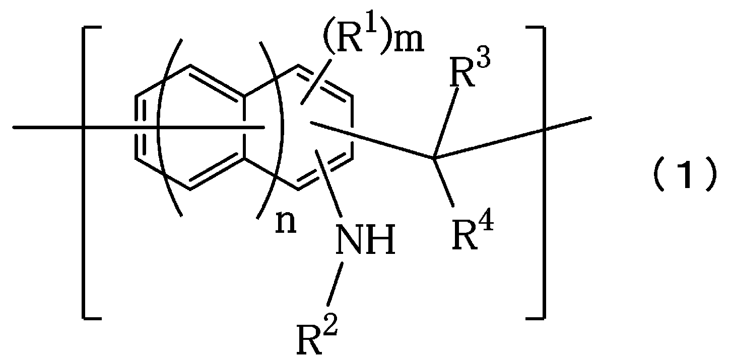
(식(1) 중, R1은 수소원자의 치환기로서, 할로겐기, 니트로기, 아미노기, 하이드록시기, 탄소수 1 내지 10의 알킬기, 탄소수 2 내지 10의 알케닐기, 탄소수 6 내지 40의 아릴기, 또는 에테르결합, 케톤결합, 혹은 에스테르결합을 포함할 수도 있는 이들의 조합이며, R2는 탄소수 1 내지 10의 알킬기, 탄소수 2 내지 10의 알케닐기, 탄소수 6 내지 40의 아릴기, 또는 에테르결합, 케톤결합, 혹은 에스테르결합을 포함할 수도 있는 이들의 조합이며, R3은 수소원자, 또는 할로겐기, 니트로기, 아미노기, 포밀기, 카르복실기, 카르본산알킬에스테르기, 하이드록시기로 치환될 수도 있는 탄소수 6 내지 40의 아릴기, 또는 복소환기이며, R4는 수소원자, 또는 할로겐기, 니트로기, 아미노기, 포밀기, 카르복실기, 카르본산알킬에스테르기, 하이드록시기로 치환될 수도 있는 탄소수 1 내지 10의 알킬기, 탄소수 6 내지 40의 아릴기, 또는 복소환기이며, R3과 R4는 이들이 결합하는 탄소원자와 함께 환을 형성할 수도 있다. n은 0 또는 1의 정수이며, m은 n이 0일 때 0 내지 3까지의 정수이며, n이 1일 때 0 내지 5까지의 정수이다.)로 표시되는 단위구조를 포함하는 것인 제1 관점에 기재된 레지스트 하층막 형성 조성물,(In formula (1), R 1 is a substituent of a hydrogen atom, and is a halogen group, a nitro group, an amino group, a hydroxy group, an alkyl group having 1 to 10 carbon atoms, an alkenyl group having 2 to 10 carbon atoms, or an aryl group having 6 to 40 carbon atoms. , or a combination thereof which may contain an ether bond, a ketone bond, or an ester bond, and R 2 is an alkyl group having 1 to 10 carbon atoms, an alkenyl group having 2 to 10 carbon atoms, an aryl group having 6 to 40 carbon atoms, or an ether bond. , a ketone bond, or a combination thereof that may contain an ester bond, and R 3 is a hydrogen atom, or a halogen group, a nitro group, an amino group, a formyl group, a carboxyl group, an alkyl carboxylate group, which may be substituted with a hydroxy group an aryl group having 6 to 40 carbon atoms or a heterocyclic group, and R 4 is a hydrogen atom, or a halogen group, a nitro group, an amino group, a formyl group, a carboxyl group, a carboxylate alkyl ester group, or a hydroxy group having 1 to 10 carbon atoms which may be substituted of an alkyl group, an aryl group having 6 to 40 carbon atoms, or a heterocyclic group, and R 3 and R 4 may form a ring together with the carbon atom to which they are bonded, n is an integer of 0 or 1, m is n is 0 is an integer from 0 to 3 when n is an integer from 0 to 5 when n is 1. The resist underlayer film forming composition according to the first aspect comprising a unit structure represented by);
제3 관점으로서, n 및 m이 제로이며, R2가 메틸기 또는 벤질기인 제2 관점에 기재된 레지스트 하층막 형성 조성물,As a 3rd viewpoint, n and m are zero, and R<2> is a methyl group or a benzyl group, The resist underlayer film forming composition of a 2nd viewpoint,
제4 관점으로서, R3이 페닐기, 나프틸기, 안트릴기, 또는 피레닐기이며, R4가 수소원자인 제2 관점 또는 제3 관점에 기재된 레지스트 하층막 형성 조성물,As a fourth aspect, R 3 is a phenyl group, a naphthyl group, an anthryl group, or a pyrenyl group, and R 4 is a hydrogen atom. The composition for forming a resist underlayer film according to the second or third aspect;
제5 관점으로서, 추가로 가교제를 함유하는 제1 관점 내지 제4 관점 중 어느 하나에 기재된 레지스트 하층막 형성 조성물,As a 5th viewpoint, the resist underlayer film forming composition in any one of 1st viewpoint thru|or 4th viewpoint which further contains a crosslinking agent;
제6 관점으로서, 추가로 산 및/또는 산발생제를 포함하는 제1 관점 내지 제5 관점 중 어느 하나에 기재된 레지스트 하층막 형성 조성물,As a sixth aspect, the resist underlayer film forming composition according to any one of the first to fifth aspects, further comprising an acid and/or an acid generator;
제7 관점으로서, 제1 관점 내지 제6 관점 중 어느 하나에 기재된 레지스트 하층막 형성 조성물을 반도체기판 상에 도포하고 소성함으로써 얻어지는 레지스트 하층막,As a seventh aspect, a resist underlayer film obtained by applying the resist underlayer film forming composition according to any one of the first to sixth aspects on a semiconductor substrate and baking it;
제8 관점으로서, 반도체기판 상에 제1 관점 내지 제6 관점 중 어느 하나에 기재된 레지스트 하층막 형성 조성물에 의해 하층막을 형성하는 공정, 그 위에 레지스트막을 형성하는 공정, 광 또는 전자선의 조사와 현상에 의해 레지스트패턴을 형성하는 공정, 형성된 레지스트패턴에 의해 이 하층막을 에칭하는 공정, 및 패턴화된 하층막에 의해 반도체기판을 가공하는 공정을 포함하는 반도체장치의 제조방법, 및As an eighth aspect, a step of forming an underlayer film on a semiconductor substrate with the resist underlayer film forming composition according to any one of the first to sixth aspects, a step of forming a resist film thereon, irradiation and development of light or electron beams A method of manufacturing a semiconductor device comprising a step of forming a resist pattern by means of a resist pattern, a step of etching the underlayer film with the formed resist pattern, and a step of processing a semiconductor substrate with the patterned underlayer film, and
제9 관점으로서, 반도체기판 상에 제1 관점 내지 제6 관점 중 어느 하나에 기재된 레지스트 하층막 형성 조성물에 의해 레지스트 하층막을 형성하는 공정, 그 위에 하드마스크를 형성하는 공정, 다시 그 위에 레지스트막을 형성하는 공정, 광 또는 전자선의 조사와 현상에 의해 레지스트패턴을 형성하는 공정, 형성된 레지스트패턴에 의해 하드마스크를 에칭하는 공정, 패턴화된 하드마스크에 의해 이 레지스트 하층막을 에칭하는 공정, 및 패턴화된 레지스트 하층막에 의해 반도체기판을 가공하는 공정을 포함하는 반도체장치의 제조방법이다.As a ninth aspect, a step of forming a resist underlayer film with the resist underlayer film forming composition according to any one of the first to sixth aspects on a semiconductor substrate, a step of forming a hard mask thereon, and further forming a resist film thereon a step of forming a resist pattern by irradiation and development of light or electron beams, a step of etching a hard mask with the formed resist pattern, a step of etching the resist underlayer film with a patterned hard mask, and It is a manufacturing method of a semiconductor device including the process of processing a semiconductor substrate with a resist underlayer film.
본 발명의 레지스트 하층막 형성 조성물에 의해, 레지스트 하층막의 상층부와 그 위에 피복되는 층의 인터믹싱을 일으키지 않고, 양호한 레지스트의 패턴형상을 형성할 수 있다.
With the resist underlayer film forming composition of the present invention, a good resist pattern can be formed without causing intermixing of the upper layer portion of the resist underlayer film and the layer coated thereon.
본 발명의 레지스트 하층막 형성 조성물에는 기판으로부터의 반사를 효율적으로 억제하는 성능을 부여하는 것도 가능하며, 노광광의 반사방지막으로서의 효과를 겸비할 수도 있다.
The composition for forming a resist underlayer film of the present invention can also be imparted with the ability to efficiently suppress reflection from the substrate, and can also have an effect as an antireflection film of exposure light.
본 발명의 레지스트 하층막 형성 조성물에 의해, 레지스트에 가까운 드라이에칭속도의 선택비, 레지스트에 비해 작은 드라이에칭속도의 선택비나 반도체기판에 비해 작은 드라이에칭속도의 선택비를 갖는, 우수한 레지스트 하층막을 제공할 수 있다.
The resist underlayer film forming composition of the present invention provides an excellent resist underlayer film having a selectivity of a dry etching rate close to that of a resist, a selectivity of a dry etching rate smaller than that of a resist, or a selectivity of a dry etching rate smaller than that of a semiconductor substrate can do.
레지스트패턴의 미세화에 수반하여 레지스트패턴이 현상 후에 무너지는 것을 방지하기 위하여 레지스트의 박막화가 행해지고 있다. 이러한 박막레지스트에서는, 레지스트패턴을 에칭프로세스에서 그 하층막에 전사하고, 그 하층막을 마스크로 하여 기판가공을 행하는 프로세스나, 레지스트패턴을 에칭프로세스에서 그 하층막에 전사하고, 다시 하층막에 전사된 패턴을 상이한 가스조성을 이용하여 그 하층막에 전사한다는 행정을 반복하여, 최종적으로 기판가공을 행하는 프로세스가 있다. 본 발명의 레지스트 하층막 및 그 형성조성물은 이 프로세스에 유효하며, 본 발명의 레지스트 하층막을 이용하여 기판을 가공할 때는, 가공기판(예를 들어, 기판상의 열산화규소막, 질화규소막, 폴리실리콘막 등)에 대하여 충분히 에칭내성을 갖는 것이다.
With the miniaturization of the resist pattern, thinning of the resist is performed in order to prevent the resist pattern from collapsing after development. In such a thin film resist, a resist pattern is transferred to the lower layer film in an etching process, and a substrate processing is performed using the lower layer film as a mask, or a resist pattern is transferred to the lower layer film in an etching process and transferred to the lower layer film again. There is a process in which the process of transferring a pattern to the underlayer film using different gas compositions is repeated, and finally substrate processing is performed. The resist underlayer film of the present invention and its formation composition are effective for this process, and when a substrate is processed using the resist underlayer film of the present invention, a processed substrate (eg, thermal silicon oxide film on a substrate, silicon nitride film, polysilicon film, etc.) has sufficient etching resistance.
그리고, 본 발명의 레지스트 하층막은, 평탄화막, 레지스트 하층막, 레지스트층의 오염방지막, 드라이에칭선택성을 갖는 막으로서 이용할 수 있다. 이에 따라, 반도체제조의 리소그래피 프로세스에 있어서의 레지스트패턴 형성을, 용이하게, 정도(精度) 좋게 행할 수 있게 된다.
The resist underlayer film of the present invention can be used as a planarization film, a resist underlayer film, a resist layer anti-contamination film, and a film having dry etching selectivity. This makes it possible to easily and accurately form a resist pattern in a lithography process for semiconductor manufacturing.
본 발명에 의한 레지스트 하층막 형성 조성물에 의해 레지스트 하층막을 기판 상에 형성하고, 그 위에 하드마스크를 형성하고, 그 위에 레지스트막을 형성하고, 노광과 현상에 의해 레지스트패턴을 형성하고, 레지스트패턴을 하드마스크에 전사하고, 하드마스크에 전사된 레지스트패턴을 레지스트 하층막에 전사하고, 그 레지스트 하층막으로 반도체기판의 가공을 행하는 프로세스가 있다. 이 프로세스에서 하드마스크는 유기폴리머나 무기폴리머와 용제를 포함하는 도포형의 조성물에 의해 행해지는 경우와, 무기물의 진공증착에 의해 행해지는 경우가 있다. 무기물(예를 들어, 질화산화규소)의 진공증착에서는 증착물이 레지스트 하층막 표면에 퇴적되는데, 이 때 레지스트 하층막 표면의 온도가 400℃ 전후로 상승한다. 본 발명에서는 이용되는 폴리머가 식(1)로 표시되는 단위구조를 포함하는 폴리머이므로 매우 내열성이 높고, 증착물의 퇴적에 의해서도 열열화를 발생시키지 않는다.A resist underlayer film is formed on a substrate with the resist underlayer film forming composition according to the present invention, a hard mask is formed thereon, a resist film is formed thereon, a resist pattern is formed by exposure and development, and the resist pattern is hard There is a process of transferring a mask to a resist pattern transferred to a hard mask, transferring the resist pattern to a resist underlayer film, and processing a semiconductor substrate with the resist underlayer film. In this process, a hard mask may be performed by the coating type composition containing an organic polymer or an inorganic polymer, and a solvent, and may be performed by vacuum deposition of an inorganic material. In vacuum deposition of an inorganic material (eg, silicon nitride oxide), a deposit is deposited on the surface of the resist underlayer, at which time the temperature of the resist underlayer surface rises to around 400°C. In the present invention, since the polymer used is a polymer having a unit structure represented by formula (1), it has very high heat resistance and does not cause thermal deterioration even by deposition of deposits.
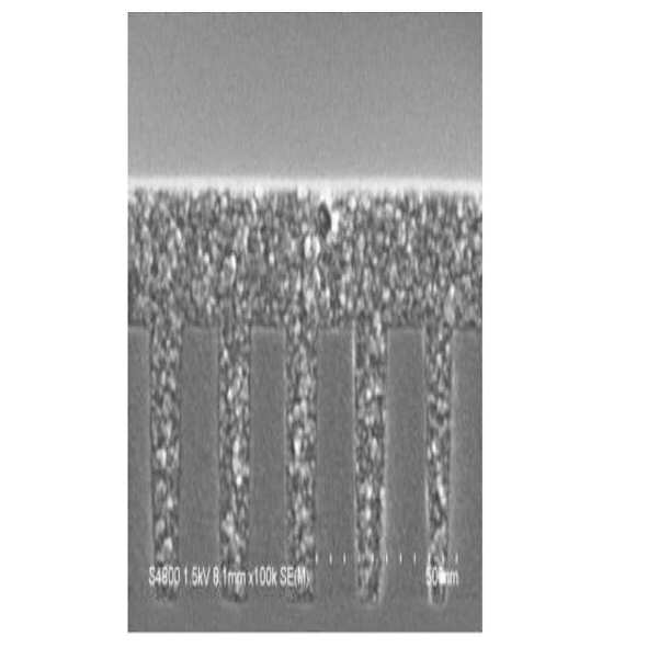
도 1은 실시예 1에서 조제된 레지스트 하층막 형성 조성물의 용액을, 스핀코터를 이용하여 홀웨이퍼 상에 도포하고, 400℃ 2분간의 소성을 행한 후의 기판의 단면을 전자현미경으로 관찰한 사진이다(배율은 10만배).
도 2는 실시예 2에서 조제된 레지스트 하층막 형성 조성물의 용액을, 스핀코터를 이용하여 홀웨이퍼 상에 도포하고, 400℃ 2분간의 소성을 행한 후의 기판의 단면을 전자현미경으로 관찰한 사진이다(배율은 10만배).
도 3은 실시예 3에서 조제된 레지스트 하층막 형성 조성물의 용액을, 스핀코터를 이용하여 홀웨이퍼 상에 도포하고, 400℃ 2분간의 소성을 행한 후의 기판의 단면을 전자현미경으로 관찰한 사진이다(배율은 10만배).
도 4는 실시예 4에서 조제된 레지스트 하층막 형성 조성물의 용액을, 스핀코터를 이용하여 홀웨이퍼 상에 도포하고, 400℃ 2분간의 소성을 행한 후의 기판의 단면을 전자현미경으로 관찰한 사진이다(배율은 10만배).
도 5는 비교예 2에서 조제된 레지스트 하층막 형성 조성물의 용액을, 스핀코터를 이용하여 홀웨이퍼 상에 도포하고, 400℃ 2분간의 소성을 행한 후의 기판의 단면을 전자현미경으로 관찰한 사진이다(배율은 10만배).1 is a photograph of a cross-section of a substrate after applying a solution of a resist underlayer film forming composition prepared in Example 1 on a hole wafer using a spin coater, and baking at 400° C. for 2 minutes, observed with an electron microscope. (The magnification is 100,000 times).
FIG. 2 is a photograph of a cross-section of a substrate after applying the solution of the resist underlayer film forming composition prepared in Example 2 on a hole wafer using a spin coater and baking at 400° C. for 2 minutes with an electron microscope. (The magnification is 100,000 times).
3 is a photograph of a cross-section of the substrate after applying the solution of the resist underlayer film forming composition prepared in Example 3 on the hole wafer using a spin coater, and baking at 400° C. for 2 minutes, observed with an electron microscope. (The magnification is 100,000 times).
4 is a photograph of a cross-section of the substrate after applying the solution of the resist underlayer film forming composition prepared in Example 4 on the hole wafer using a spin coater, and baking at 400° C. for 2 minutes, observed with an electron microscope. (The magnification is 100,000 times).
5 is a photograph of a cross-section of a substrate after applying a solution of a resist underlayer film forming composition prepared in Comparative Example 2 on a hole wafer using a spin coater and baking at 400° C. for 2 minutes with an electron microscope. (The magnification is 100,000 times).
본 발명은 제2 아미노기를 갖는 방향족 화합물과 알데히드 화합물의 반응에 의해 얻어지는 노볼락수지를 포함하는, 리소그래피 공정에 이용하는 레지스트 하층막 형성 조성물이다.
The present invention is a composition for forming a resist underlayer film for use in a lithography process, comprising a novolak resin obtained by reaction of an aromatic compound having a second amino group and an aldehyde compound.
또한, 본 발명은 식(1)로 표시되는 단위구조를 포함하는 노볼락수지를 포함하는 리소그래피 공정에 이용하는 레지스트 하층막 형성 조성물이다.Further, the present invention is a resist underlayer film forming composition for use in a lithography process containing a novolak resin having a unit structure represented by formula (1).
본 발명에 있어서 상기의 리소그래피용 레지스트 하층막 형성 조성물은 상기 폴리머와 용제를 포함한다. 그리고, 가교제와 산을 포함할 수 있고, 필요에 따라 산발생제, 계면활성제 등의 첨가제를 포함할 수 있다. 이 조성물의 고형분은 0.1 내지 70질량%, 또는 0.1 내지 60질량%이다. 여기서, 고형분은 레지스트 하층막 형성 조성물로부터 용제를 제거한 전체 성분의 함유비율이다. 고형분 중에 상기 폴리머를 1 내지 100질량%, 또는 1 내지 99.9질량%, 또는 50 내지 99.9질량%, 또는 50 내지 95질량%, 또는 50 내지 90질량%의 비율로 함유할 수 있다.In the present invention, the composition for forming a resist underlayer film for lithography includes the polymer and the solvent. And, it may include a crosslinking agent and an acid, and may include additives such as an acid generator and a surfactant if necessary. Solid content of this composition is 0.1-70 mass %, or 0.1-60 mass %. Here, the solid content is the content ratio of the total components obtained by removing the solvent from the resist underlayer film forming composition. The polymer may be contained in a proportion of 1 to 100% by mass, or 1 to 99.9% by mass, or 50 to 99.9% by mass, or 50 to 95% by mass, or 50 to 90% by mass in the solid content.
본 발명에 이용되는 폴리머는, 중량평균 분자량이 600 내지 1000000, 또는 600 내지 200000이다.The polymer used in the present invention has a weight average molecular weight of 600 to 1000000, or 600 to 200000.
식(1) 중, R1은 수소원자의 치환기로서, 할로겐기, 니트로기, 아미노기, 하이드록시기, 탄소수 1 내지 10의 알킬기, 탄소수 2 내지 10의 알케닐기, 탄소수 6 내지 40의 아릴기, 또는 에테르결합, 케톤결합, 혹은 에스테르결합을 포함할 수도 있는 이들의 조합이며, R2는 탄소수 1 내지 10의 알킬기, 탄소수 2 내지 10의 알케닐기, 탄소수 6 내지 40의 아릴기, 또는 에테르결합, 케톤결합, 혹은 에스테르결합을 포함할 수도 있는 이들의 조합이며, R3은 수소원자, 또는 할로겐기, 니트로기, 아미노기, 포밀기, 카르복실기, 카르본산알킬에스테르기, 하이드록시기로 치환될 수도 있는 탄소수 6 내지 40의 아릴기, 또는 복소환기이며, R4는 수소원자, 또는 할로겐기, 니트로기, 아미노기, 포밀기, 카르복실기, 카르본산알킬에스테르기, 하이드록시기로 치환될 수도 있는 탄소수 1 내지 10의 알킬기, 탄소수 6 내지 40의 아릴기, 또는 복소환기이며, R3과 R4는 이들이 결합하는 탄소원자와 함께 환을 형성할 수도 있다. n은 0 또는 1의 정수이며, m은 n이 0일 때 0 내지 3까지의 정수이며, n이 1일 때 0 내지 5까지의 정수이다.
In formula (1), R 1 is a substituent of a hydrogen atom, and is a halogen group, a nitro group, an amino group, a hydroxy group, an alkyl group having 1 to 10 carbon atoms, an alkenyl group having 2 to 10 carbon atoms, an aryl group having 6 to 40 carbon atoms, or a combination thereof which may contain an ether bond, a ketone bond, or an ester bond, R 2 is an alkyl group having 1 to 10 carbon atoms, an alkenyl group having 2 to 10 carbon atoms, an aryl group having 6 to 40 carbon atoms, or an ether bond; A ketone bond or a combination thereof which may contain an ester bond, and R 3 is a hydrogen atom, or a number of carbon atoms that may be substituted with a halogen group, a nitro group, an amino group, a formyl group, a carboxyl group, an alkyl carboxylic acid ester group, or a hydroxy group. 6 to 40 aryl group, or a heterocyclic group, R 4 is a hydrogen atom, or a halogen group, a nitro group, an amino group, a formyl group, a carboxyl group, a carboxylic acid alkyl ester group, a hydroxy group having 1 to 10 carbon atoms which may be substituted an alkyl group, an aryl group having 6 to 40 carbon atoms, or a heterocyclic group, and R 3 and R 4 may form a ring together with the carbon atom to which they are bonded. n is an integer of 0 or 1, m is an integer from 0 to 3 when n is 0, and an integer from 0 to 5 when n is 1.
여기서, 상기 탄소수 1 내지 10의 알킬기로는 메틸기, 에틸기, n-프로필기, i-프로필기, 시클로프로필기, n-부틸기, i-부틸기, s-부틸기, t-부틸기, 시클로부틸기, 1-메틸-시클로프로필기, 2-메틸-시클로프로필기, n-펜틸기, 1-메틸-n-부틸기, 2-메틸-n-부틸기, 3-메틸-n-부틸기, 1,1-디메틸-n-프로필기, 1,2-디메틸-n-프로필기, 2,2-디메틸-n-프로필기, 1-에틸-n-프로필기, 시클로펜틸기, 1-메틸-시클로부틸기, 2-메틸-시클로부틸기, 3-메틸-시클로부틸기, 1,2-디메틸-시클로프로필기, 2,3-디메틸-시클로프로필기, 1-에틸-시클로프로필기, 2-에틸-시클로프로필기, n-헥실기, 1-메틸-n-펜틸기, 2-메틸-n-펜틸기, 3-메틸-n-펜틸기, 4-메틸-n-펜틸기, 1,1-디메틸-n-부틸기, 1,2-디메틸-n-부틸기, 1,3-디메틸-n-부틸기, 2,2-디메틸-n-부틸기, 2,3-디메틸-n-부틸기, 3,3-디메틸-n-부틸기, 1-에틸-n-부틸기, 2-에틸-n-부틸기, 1,1,2-트리메틸-n-프로필기, 1,2,2-트리메틸-n-프로필기, 1-에틸-1-메틸-n-프로필기, 1-에틸-2-메틸-n-프로필기, 시클로헥실기, 1-메틸-시클로펜틸기, 2-메틸-시클로펜틸기, 3-메틸-시클로펜틸기, 1-에틸-시클로부틸기, 2-에틸-시클로부틸기, 3-에틸-시클로부틸기, 1,2-디메틸-시클로부틸기, 1,3-디메틸-시클로부틸기, 2,2-디메틸-시클로부틸기, 2,3-디메틸-시클로부틸기, 2,4-디메틸-시클로부틸기, 3,3-디메틸-시클로부틸기, 1-n-프로필-시클로프로필기, 2-n-프로필-시클로프로필기, 1-i-프로필-시클로프로필기, 2-i-프로필-시클로프로필기, 1,2,2-트리메틸-시클로프로필기, 1,2,3-트리메틸-시클로프로필기, 2,2,3-트리메틸-시클로프로필기, 1-에틸-2-메틸-시클로프로필기, 2-에틸-1-메틸-시클로프로필기, 2-에틸-2-메틸-시클로프로필기 및 2-에틸-3-메틸-시클로프로필기 등을 들 수 있다.
Here, the alkyl group having 1 to 10 carbon atoms is a methyl group, ethyl group, n-propyl group, i-propyl group, cyclopropyl group, n-butyl group, i-butyl group, s-butyl group, t-butyl group, cyclo Butyl group, 1-methyl-cyclopropyl group, 2-methyl-cyclopropyl group, n-pentyl group, 1-methyl-n-butyl group, 2-methyl-n-butyl group, 3-methyl-n-butyl group , 1,1-dimethyl-n-propyl group, 1,2-dimethyl-n-propyl group, 2,2-dimethyl-n-propyl group, 1-ethyl-n-propyl group, cyclopentyl group, 1-methyl -Cyclobutyl group, 2-methyl-cyclobutyl group, 3-methyl-cyclobutyl group, 1,2-dimethyl-cyclopropyl group, 2,3-dimethyl-cyclopropyl group, 1-ethyl-cyclopropyl group, 2 -Ethyl-cyclopropyl group, n-hexyl group, 1-methyl-n-pentyl group, 2-methyl-n-pentyl group, 3-methyl-n-pentyl group, 4-methyl-n-pentyl group, 1, 1-dimethyl-n-butyl group, 1,2-dimethyl-n-butyl group, 1,3-dimethyl-n-butyl group, 2,2-dimethyl-n-butyl group, 2,3-dimethyl-n- Butyl group, 3,3-dimethyl-n-butyl group, 1-ethyl-n-butyl group, 2-ethyl-n-butyl group, 1,1,2-trimethyl-n-propyl group, 1,2,2 -Trimethyl-n-propyl group, 1-ethyl-1-methyl-n-propyl group, 1-ethyl-2-methyl-n-propyl group, cyclohexyl group, 1-methyl-cyclopentyl group, 2-methyl- Cyclopentyl group, 3-methyl-cyclopentyl group, 1-ethyl-cyclobutyl group, 2-ethyl-cyclobutyl group, 3-ethyl-cyclobutyl group, 1,2-dimethyl-cyclobutyl group, 1,3- Dimethyl-cyclobutyl group, 2,2-dimethyl-cyclobutyl group, 2,3-dimethyl-cyclobutyl group, 2,4-dimethyl-cyclobutyl group, 3,3-dimethyl-cyclobutyl group, 1-n- Propyl-cyclopropyl group, 2-n-propyl-cyclopropyl group, 1-i-propyl-cyclopropyl group, 2-i-propyl-cyclopropyl group, 1,2,2-trimethyl-cyclopropyl group, 1, 2,3-trimethyl-cyclopropyl group, 2,2,3-trimethyl-cyclopropyl group, 1-ethyl-2-methyl-cyclopropyl group, 2-ethyl-1-methyl-cyclopropyl group, 2-ethyl- 2-methyl-cyclopropyl group, 2-ethyl-3-methyl-cyclopropyl group, etc. are mentioned.
상기 탄소수 2 내지 10의 알케닐기로는 에테닐기, 1-프로페닐기, 2-프로페닐기, 1-메틸-1-에테닐기, 1-부테닐기, 2-부테닐기, 3-부테닐기, 2-메틸-1-프로페닐기, 2-메틸-2-프로페닐기, 1-에틸에테닐기, 1-메틸-1-프로페닐기, 1-메틸-2-프로페닐기, 1-펜테닐기, 2-펜테닐기, 3-펜테닐기, 4-펜테닐기, 1-n-프로필에테닐기, 1-메틸-1-부테닐기, 1-메틸-2-부테닐기, 1-메틸-3-부테닐기, 2-에틸-2-프로페닐기, 2-메틸-1-부테닐기, 2-메틸-2-부테닐기, 2-메틸-3-부테닐기, 3-메틸-1-부테닐기, 3-메틸-2-부테닐기, 3-메틸-3-부테닐기, 1,1-디메틸-2-프로페닐기, 1-i-프로필에테닐기, 1,2-디메틸-1-프로페닐기, 1,2-디메틸-2-프로페닐기, 1-시클로펜테닐기, 2-시클로펜테닐기, 3-시클로펜테닐기, 1-헥세닐기, 2-헥세닐기, 3-헥세닐기, 4-헥세닐기, 5-헥세닐기, 1-메틸-1-펜테닐기, 1-메틸-2-펜테닐기, 1-메틸-3-펜테닐기, 1-메틸-4-펜테닐기, 1-n-부틸에테닐기, 2-메틸-1-펜테닐기, 2-메틸-2-펜테닐기, 2-메틸-3-펜테닐기, 2-메틸-4-펜테닐기, 2-n-프로필-2-프로페닐기, 3-메틸-1-펜테닐기, 3-메틸-2-펜테닐기, 3-메틸-3-펜테닐기, 3-메틸-4-펜테닐기, 3-에틸-3-부테닐기, 4-메틸-1-펜테닐기, 4-메틸-2-펜테닐기, 4-메틸-3-펜테닐기, 4-메틸-4-펜테닐기, 1,1-디메틸-2-부테닐기, 1,1-디메틸-3-부테닐기, 1,2-디메틸-1-부테닐기, 1,2-디메틸-2-부테닐기, 1,2-디메틸-3-부테닐기, 1-메틸-2-에틸-2-프로페닐기, 1-s-부틸에테닐기, 1,3-디메틸-1-부테닐기, 1,3-디메틸-2-부테닐기, 1,3-디메틸-3-부테닐기, 1-i-부틸에테닐기, 2,2-디메틸-3-부테닐기, 2,3-디메틸-1-부테닐기, 2,3-디메틸-2-부테닐기, 2,3-디메틸-3-부테닐기, 2-i-프로필-2-프로페닐기, 3,3-디메틸-1-부테닐기, 1-에틸-1-부테닐기, 1-에틸-2-부테닐기, 1-에틸-3-부테닐기, 1-n-프로필-1-프로페닐기, 1-n-프로필-2-프로페닐기, 2-에틸-1-부테닐기, 2-에틸-2-부테닐기, 2-에틸-3-부테닐기, 1,1,2-트리메틸-2-프로페닐기, 1-t-부틸에테닐기, 1-메틸-1-에틸-2-프로페닐기, 1-에틸-2-메틸-1-프로페닐기, 1-에틸-2-메틸-2-프로페닐기, 1-i-프로필-1-프로페닐기, 1-i-프로필-2-프로페닐기, 1-메틸-2-시클로펜테닐기, 1-메틸-3-시클로펜테닐기, 2-메틸-1-시클로펜테닐기, 2-메틸-2-시클로펜테닐기, 2-메틸-3-시클로펜테닐기, 2-메틸-4-시클로펜테닐기, 2-메틸-5-시클로펜테닐기, 2-메틸렌-시클로펜틸기, 3-메틸-1-시클로펜테닐기, 3-메틸-2-시클로펜테닐기, 3-메틸-3-시클로펜테닐기, 3-메틸-4-시클로펜테닐기, 3-메틸-5-시클로펜테닐기, 3-메틸렌-시클로펜틸기, 1-시클로헥세닐기, 2-시클로헥세닐기 및 3-시클로헥세닐기 등을 들 수 있다.
Examples of the alkenyl group having 2 to 10 carbon atoms include ethenyl group, 1-propenyl group, 2-propenyl group, 1-methyl-1-ethenyl group, 1-butenyl group, 2-butenyl group, 3-butenyl group, and 2-methyl group. -1-propenyl group, 2-methyl-2-propenyl group, 1-ethylethenyl group, 1-methyl-1-propenyl group, 1-methyl-2-propenyl group, 1-pentenyl group, 2-pentenyl group, 3-pentenyl group, 4-pentenyl group, 1-n-propylethenyl group, 1-methyl-1-butenyl group, 1-methyl-2-butenyl group, 1-methyl-3-butenyl group, 2-ethyl- 2-propenyl group, 2-methyl-1-butenyl group, 2-methyl-2-butenyl group, 2-methyl-3-butenyl group, 3-methyl-1-butenyl group, 3-methyl-2-butenyl group, 3-methyl-3-butenyl group, 1,1-dimethyl-2-propenyl group, 1-i-propylethenyl group, 1,2-dimethyl-1-propenyl group, 1,2-dimethyl-2-propenyl group , 1-cyclopentenyl group, 2-cyclopentenyl group, 3-cyclopentenyl group, 1-hexenyl group, 2-hexenyl group, 3-hexenyl group, 4-hexenyl group, 5-hexenyl group, 1 -Methyl-1-pentenyl group, 1-methyl-2-pentenyl group, 1-methyl-3-pentenyl group, 1-methyl-4-pentenyl group, 1-n-butylethenyl group, 2-methyl-1- Pentenyl group, 2-methyl-2-pentenyl group, 2-methyl-3-pentenyl group, 2-methyl-4-pentenyl group, 2-n-propyl-2-propenyl group, 3-methyl-1-pentenyl group, 3-methyl-2-pentenyl group, 3-methyl-3-pentenyl group, 3-methyl-4-pentenyl group, 3-ethyl-3-butenyl group, 4-methyl-1-pentenyl group, 4-methyl-2 -pentenyl group, 4-methyl-3-pentenyl group, 4-methyl-4-pentenyl group, 1,1-dimethyl-2-butenyl group, 1,1-dimethyl-3-butenyl group, 1,2-dimethyl- 1-butenyl group, 1,2-dimethyl-2-butenyl group, 1,2-dimethyl-3-butenyl group, 1-methyl-2-ethyl-2-propenyl group, 1-s-butylethenyl group, 1 ,3-dimethyl-1-butenyl group, 1,3-dimethyl-2-butenyl group, 1,3-dimethyl-3-butenyl group, 1-i-butylethenyl group, 2,2-dimethyl-3-bute Nyl group, 2,3-dimethyl-1-butenyl group, 2,3-dimethyl-2-butenyl group, 2,3-dimethyl-3-butenyl group, 2-i-propyl-2-propenyl group, 3,3- Dimethyl-1-butenyl group, 1-ethyl-1-butenyl group, 1-ethyl-2 -Butenyl group, 1-ethyl-3-butenyl group, 1-n-propyl-1-propenyl group, 1-n-propyl-2-propenyl group, 2-ethyl-1-butenyl group, 2-ethyl-2- Butenyl group, 2-ethyl-3-butenyl group, 1,1,2-trimethyl-2-propenyl group, 1-t-butylethenyl group, 1-methyl-1-ethyl-2-propenyl group, 1-ethyl -2-methyl-1-propenyl group, 1-ethyl-2-methyl-2-propenyl group, 1-i-propyl-1-propenyl group, 1-i-propyl-2-propenyl group, 1-methyl-2 -Cyclopentenyl group, 1-methyl-3-cyclopentenyl group, 2-methyl-1-cyclopentenyl group, 2-methyl-2-cyclopentenyl group, 2-methyl-3-cyclopentenyl group, 2-methyl-4 -Cyclopentenyl group, 2-methyl-5-cyclopentenyl group, 2-methylene-cyclopentyl group, 3-methyl-1-cyclopentenyl group, 3-methyl-2-cyclopentenyl group, 3-methyl-3-cyclo Pentenyl group, 3-methyl-4-cyclopentenyl group, 3-methyl-5-cyclopentenyl group, 3-methylene-cyclopentyl group, 1-cyclohexenyl group, 2-cyclohexenyl group and 3-cyclohexenyl group and the like.
상기 탄소수 6 내지 40의 아릴기로는 페닐기, o-메틸페닐기, m-메틸페닐기, p-메틸페닐기, o-클로르페닐기, m-클로르페닐기, p-클로르페닐기, o-플루오로페닐기, p-플루오로페닐기, o-메톡시페닐기, p-메톡시페닐기, p-니트로페닐기, p-시아노페닐기, α-나프틸기, β-나프틸기, o-비페닐릴기, m-비페닐릴기, p-비페닐릴기, 1-안트릴기, 2-안트릴기, 9-안트릴기, 1-페난트릴기, 2-페난트릴기, 3-페난트릴기, 4-페난트릴기, 9-페난트릴기, 및 피레닐기를 들 수 있다.
The aryl group having 6 to 40 carbon atoms includes a phenyl group, o-methylphenyl group, m-methylphenyl group, p-methylphenyl group, o-chlorophenyl group, m-chlorophenyl group, p-chlorophenyl group, o-fluorophenyl group, p-fluoro lophenyl group, o-methoxyphenyl group, p-methoxyphenyl group, p-nitrophenyl group, p-cyanophenyl group, α-naphthyl group, β-naphthyl group, o-biphenylyl group, m-biphenylyl group, p- Biphenylyl group, 1-anthryl group, 2-anthryl group, 9-anthryl group, 1-phenanthryl group, 2-phenanthryl group, 3-phenanthryl group, 4-phenanthryl group, 9-phenanthryl group group, and a pyrenyl group.
상기 복소환기로는 질소, 황, 산소를 포함하는 5 내지 6원환의 복소환으로 이루어진 유기기가 바람직하고, 예를 들어 피롤기, 푸란기, 티오펜기, 이미다졸기, 옥사졸기, 티아졸기, 피라졸기, 이소옥사졸기, 이소티아졸기, 피리딘기 등을 들 수 있다.
The heterocyclic group is preferably an organic group consisting of a 5- to 6-membered heterocyclic ring containing nitrogen, sulfur, and oxygen, for example, a pyrrole group, a furan group, a thiophene group, an imidazole group, an oxazole group, a thiazole group, A pyrazole group, an isoxazole group, an isothiazole group, a pyridine group, etc. are mentioned.
상기 하이드록시기로 치환될 수도 있는 탄소수 6 내지 40의 아릴기로는 예를 들어 페놀, 디하이드록시벤젠, 트리하이드록시벤젠, 나프톨, 디하이드록시나프탈렌, 트리하이드록시나프탈렌, 하이드록시안트라센, 디하이드록시안트라센, 트리하이드록시안트라센 등을 들 수 있다.
Examples of the aryl group having 6 to 40 carbon atoms that may be substituted with the hydroxyl group include phenol, dihydroxybenzene, trihydroxybenzene, naphthol, dihydroxynaphthalene, trihydroxynaphthalene, hydroxyanthracene, dihydroxy Anthracene, trihydroxy anthracene, etc. are mentioned.
상기 카르본산알킬에스테르기의 알킬기로는 상기 탄소수 1 내지 10의 알킬기를 들 수 있다.
As an alkyl group of the said carboxylic acid alkylester group, the said C1-C10 alkyl group is mentioned.
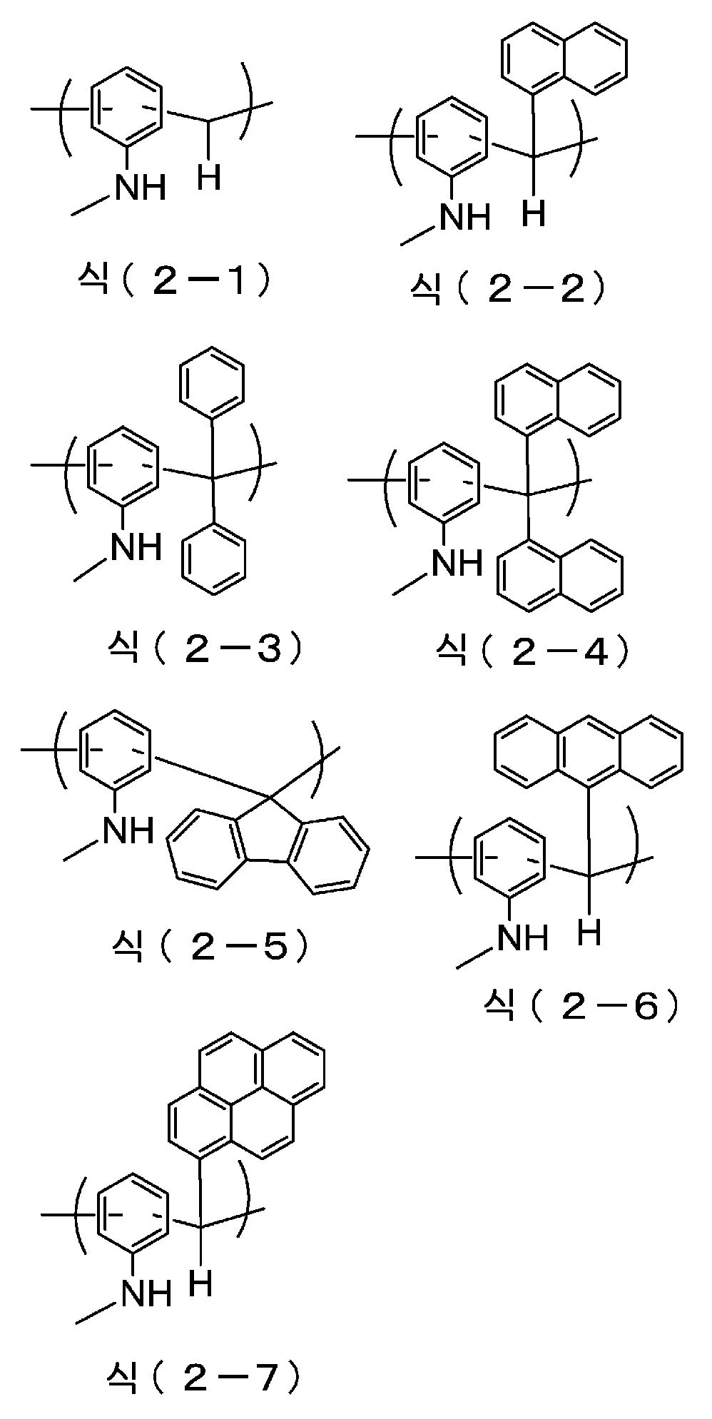
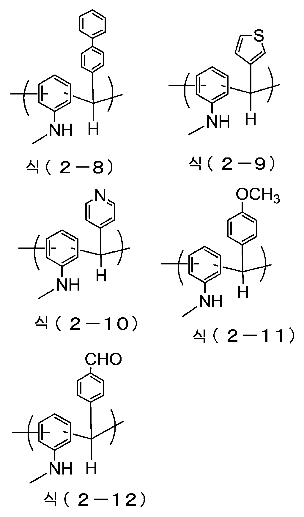
식(1)에 있어서, n 및 m이 제로이며, R2가 메틸기 또는 벤질기인 경우의 단위구조를 이용할 수 있다. 또한, 식(1)에 있어서, R2가 상기 알킬기와 아릴기의 조합에 의해 아랄킬기를 선택할 수 있다. 아랄킬기로는 벤질기, 페네틸기 등을 들 수 있다.In the formula (1), a unit structure in the case where n and m are zero and R 2 is a methyl group or a benzyl group can be used. Moreover, in Formula (1), R<2> can select an aralkyl group by the combination of the said alkyl group and an aryl group. A benzyl group, a phenethyl group, etc. are mentioned as an aralkyl group.
그리고, R3이 페닐기, 나프틸기, 안트릴기, 또는 피레닐기이며, R4가 수소원자인 경우의 단위구조를 이용할 수 있다. 나아가, R3과 R4에 있어서, 이들이 결합하는 탄소원자와 함께 형성하는 환은, 예를 들어 플루오렌환을 들 수 있다.
In addition, a unit structure in the case where R 3 is a phenyl group, a naphthyl group, an anthryl group, or a pyrenyl group and R 4 is a hydrogen atom may be used. Further, in R 3 and R 4 , the ring formed together with the carbon atom to which they are bonded includes, for example, a fluorene ring.
본 발명에 있어서의 노볼락수지는, 제2 아미노기를 갖는 방향족 화합물과, 알데히드류 또는 케톤류의 사이의 축합반응에 의해, 식(1)로 표시되는 단위구조가 형성되어 얻어진다.
The novolak resin in the present invention is obtained by forming a unit structure represented by Formula (1) by a condensation reaction between an aromatic compound having a second amino group and aldehydes or ketones.
제2 아미노기를 갖는 방향족 화합물로는, 벤젠유도체, 나프탈렌유도체이며, 상기 서술에 예시되는 치환기를 가질 수 있다.
Examples of the aromatic compound having a second amino group include a benzene derivative and a naphthalene derivative, and may have a substituent exemplified in the above description.
본 발명의 폴리머의 제조에 이용되는 알데히드류로는 포름알데히드, 파라포름알데히드, 아세트알데히드, 프로필알데히드, 부틸알데히드, 이소부틸알데히드, 발레르알데히드, 카프론알데히드, 2-메틸부틸알데히드, 헥실알데히드, 운데칸알데히드, 7-메톡시-3,7-디메틸옥틸알데히드, 시클로헥산알데히드, 3-메틸-2-부틸알데히드, 글리옥살, 말론알데히드, 석신알데히드, 글루타르알데히드, 글루타르알데히드, 아디프알데히드 등의 포화지방족 알데히드류, 아크롤레인, 메타크롤레인 등의 불포화지방족 알데히드류, 푸르푸랄, 피리딘알데히드 등의 헤테로환식 알데히드류, 벤즈알데히드, 나프틸알데히드, 안트릴알데히드, 페난트릴알데히드, 살리실알데히드, 페닐아세트알데히드, 3-페닐프로피온알데히드, 톨릴알데히드, (N,N-디메틸아미노)벤즈알데히드, 아세톡시벤즈알데히드, 1-피렌카르복시알데히드, 아니스알데히드, 테레프탈알데히드 등의 방향족 알데히드류 등을 들 수 있다. 특히 방향족 알데히드를 바람직하게 이용할 수 있다.The aldehydes used in the preparation of the polymer of the present invention include formaldehyde, paraformaldehyde, acetaldehyde, propylaldehyde, butyraldehyde, isobutylaldehyde, valeraldehyde, capronaldehyde, 2-methylbutylaldehyde, hexylaldehyde, and unde. Canaldehyde, 7-methoxy-3,7-dimethyloctylaldehyde, cyclohexanealdehyde, 3-methyl-2-butylaldehyde, glyoxal, malonaldehyde, succinaldehyde, glutaraldehyde, glutaraldehyde, adiphaldehyde, etc. Saturated aliphatic aldehydes of and aromatic aldehydes such as aldehyde, 3-phenylpropionaldehyde, tolylaldehyde, (N,N-dimethylamino)benzaldehyde, acetoxybenzaldehyde, 1-pyrenecarboxyaldehyde, anisaldehyde and terephthalaldehyde. In particular, an aromatic aldehyde can be preferably used.
또한, 본 발명의 폴리머의 제조에 이용되는 케톤류로는 디아릴케톤류이며, 예를 들어 디페닐케톤, 페닐나프틸케톤, 디나프틸케톤, 페닐톨릴케톤, 디톨릴케톤, 9-플루오레논 등을 들 수 있다.
The ketones used in the production of the polymer of the present invention are diaryl ketones, for example, diphenyl ketone, phenylnaphthyl ketone, dinaphthyl ketone, phenyltolyl ketone, ditolyl ketone, 9-fluorenone, etc. can be heard
이 축합반응에서는 1몰의 제2 아미노기를 갖는 방향족 화합물에 대하여, 알데히드류 또는 케톤류를 0.1 내지 10몰의 비율로 이용할 수 있다.In this condensation reaction, 0.1 to 10 moles of aldehydes or ketones can be used with respect to 1 mole of the aromatic compound having the second amino group.
상기 축합반응에서 이용되는 산촉매로는, 예를 들어 황산, 인산, 과염소산 등의 무기산류, p-톨루엔설폰산, p-톨루엔설폰산일수화물 등의 유기설폰산류, 포름산, 옥살산 등의 카르본산류가 사용된다. 산촉매의 사용량은, 사용하는 산류의 종류에 따라 다양하게 선택된다.Examples of the acid catalyst used in the condensation reaction include inorganic acids such as sulfuric acid, phosphoric acid and perchloric acid, organic sulfonic acids such as p-toluenesulfonic acid and p-toluenesulfonic acid monohydrate, and carboxylic acids such as formic acid and oxalic acid. used The amount of the acid catalyst to be used is variously selected depending on the type of acid to be used.
통상, 제2 아미노기를 갖는 방향족 화합물 100질량부에 대하여, 산촉매를 0.001 내지 10000질량부, 바람직하게는, 0.01 내지 1000질량부, 보다 바람직하게는 0.1 내지 100질량부의 비율로 첨가할 수 있다.
Usually, it is 0.001-10000 mass parts of an acid catalyst with respect to 100 mass parts of aromatic compounds which have a 2nd amino group, Preferably it is 0.01-1000 mass parts, More preferably, it can add in the ratio of 0.1-100 mass parts.
상기의 축합반응은 무용제로도 행해지나, 통상 용제를 이용하여 행해진다. 용제로는 반응을 저해하지 않는 것이면 전부 사용할 수 있다. 예를 들어 테트라하이드로퓨란, 디옥산 등의 환상에테르류를 들 수 있다. 또한, 사용하는 산촉매가 예를 들어 포름산과 같은 액상인 것이면 용제로서의 역할을 겸할 수도 있다.Although the above-mentioned condensation reaction is carried out also without a solvent, it is usually carried out using a solvent. As the solvent, any solvent that does not inhibit the reaction can be used. For example, cyclic ethers, such as tetrahydrofuran and a dioxane, are mentioned. In addition, as long as the acid catalyst to be used is liquid, for example, formic acid, it can also serve as a solvent.
축합시의 반응온도는 통상 40℃ 내지 200℃이다. 반응시간은 반응온도에 따라 다양하게 선택되나, 통상 30분 내지 50시간 정도이다.The reaction temperature at the time of condensation is usually 40°C to 200°C. The reaction time is variously selected depending on the reaction temperature, but is usually about 30 minutes to 50 hours.
이상과 같이 하여 얻어지는 중합체의 중량평균 분자량Mw은, 통상 500 내지 1000000, 또는 600 내지 200000이다.
The weight average molecular weight Mw of the polymer obtained by making it above is 500-1000000 normally, or 600-20000.
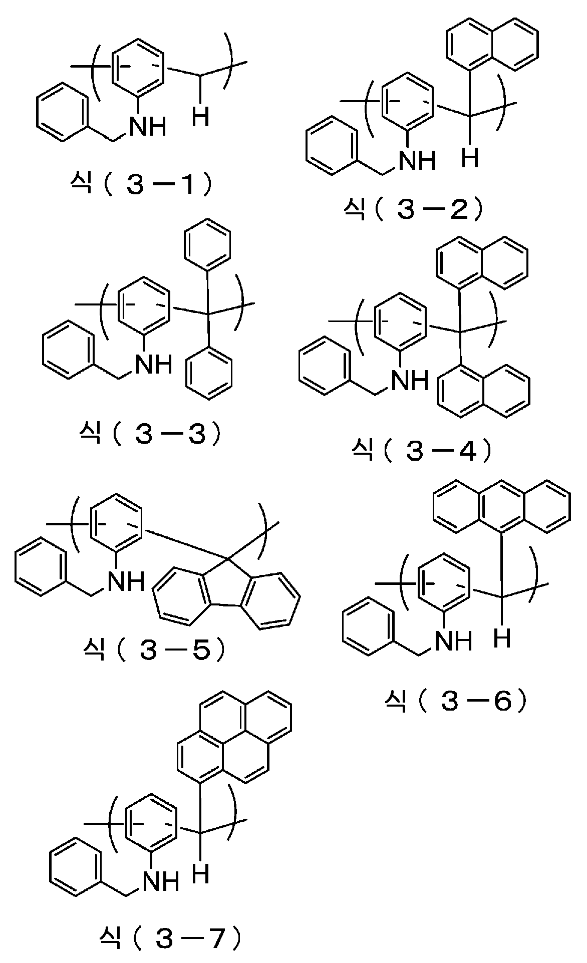
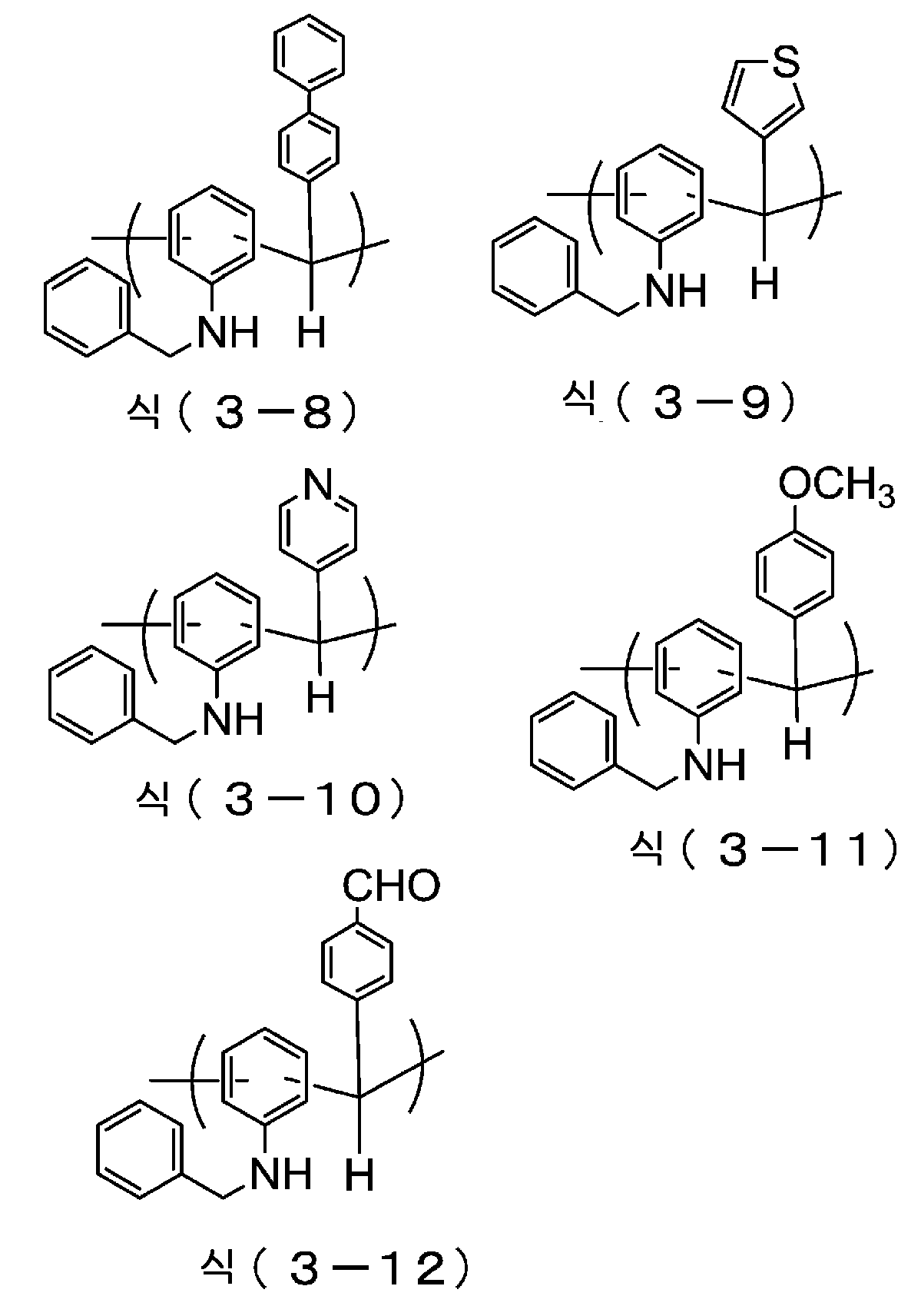
식(1)로 표시되는 단위구조를 포함하는 폴리머는 예를 들어 이하에 예시하는 식(2-1) 내지 식(2-12), 및 식(3-1) 내지 식(3-12)에 나타낼 수 있다.The polymer containing the unit structure represented by Formula (1) is, for example, represented by Formulas (2-1) to (2-12) and Formulas (3-1) to (3-12) illustrated below. can indicate
[화학식 2][Formula 2]
[화학식 3][Formula 3]
[화학식 4][Formula 4]
[화학식 5][Formula 5]
상기 폴리머는 다른 폴리머를 전체 폴리머 중에 30질량% 이내로 혼합하여 이용할 수 있다.
The polymer may be used by mixing other polymers within 30% by mass of the total polymer.
이들 폴리머로는 폴리아크릴산에스테르 화합물, 폴리메타크릴산에스테르 화합물, 폴리아크릴아미드 화합물, 폴리메타크릴아미드 화합물, 폴리비닐 화합물, 폴리스티렌 화합물, 폴리말레이미드 화합물, 폴리말레산무수물, 및 폴리아크릴로니트릴 화합물을 들 수 있다.
Examples of these polymers include polyacrylic acid ester compounds, polymethacrylic acid ester compounds, polyacrylamide compounds, polymethacrylamide compounds, polyvinyl compounds, polystyrene compounds, polymaleimide compounds, polymaleic anhydride, and polyacrylonitrile compounds. can be heard
폴리아크릴산에스테르 화합물의 원료모노머로는, 메틸아크릴레이트, 에틸아크릴레이트, 이소프로필아크릴레이트, 벤질아크릴레이트, 나프틸아크릴레이트, 안트릴아크릴레이트, 안트릴메틸아크릴레이트, 페닐아크릴레이트, 2-하이드록시에틸아크릴레이트, 2-하이드록시프로필아크릴레이트, 2,2,2-트리플루오로에틸아크릴레이트, 4-하이드록시부틸아크릴레이트, 이소부틸아크릴레이트, tert-부틸아크릴레이트, 시클로헥실아크릴레이트, 이소보닐아크릴레이트, 2-메톡시에틸아크릴레이트, 메톡시트리에틸렌글리콜아크릴레이트, 2-에톡시에틸아크릴레이트, 테트라하이드로푸르푸릴아크릴레이트, 3-메톡시부틸아크릴레이트, 2-메틸-2-아다만틸아크릴레이트, 2-에틸-2-아다만틸아크릴레이트, 2-프로필-2-아다만틸아크릴레이트, 2-메톡시부틸-2-아다만틸아크릴레이트, 8-메틸-8-트리시클로데실아크릴레이트, 8-에틸-8-트리시클로데실아크릴레이트, 및 5-아크릴로일옥시-6-하이드록시노보넨-2-카르복실릭-6-락톤 등을 들 수 있다.
Examples of the raw material monomer for the polyacrylic acid ester compound include methyl acrylate, ethyl acrylate, isopropyl acrylate, benzyl acrylate, naphthyl acrylate, anthryl acrylate, anthryl methyl acrylate, phenyl acrylate, and 2-hydride. hydroxyethyl acrylate, 2-hydroxypropyl acrylate, 2,2,2-trifluoroethyl acrylate, 4-hydroxybutyl acrylate, isobutyl acrylate, tert-butyl acrylate, cyclohexyl acrylate, Isobornyl acrylate, 2-methoxyethyl acrylate, methoxytriethylene glycol acrylate, 2-ethoxyethyl acrylate, tetrahydrofurfuryl acrylate, 3-methoxybutyl acrylate, 2-methyl-2- Adamantyl acrylate, 2-ethyl-2-adamantyl acrylate, 2-propyl-2-adamantyl acrylate, 2-methoxybutyl-2-adamantyl acrylate, 8-methyl-8- and tricyclodecyl acrylate, 8-ethyl-8-tricyclodecyl acrylate, and 5-acryloyloxy-6-hydroxynorbornene-2-carboxylic-6-lactone.
폴리메타크릴산에스테르 화합물의 원료모노머로는, 에틸메타크릴레이트, 노말프로필메타크릴레이트, 노말펜틸메타크릴레이트, 시클로헥실메타크릴레이트, 벤질메타크릴레이트, 나프틸메타크릴레이트, 안트릴메타크릴레이트, 안트릴메틸메타크릴레이트, 페닐메타크릴레이트, 2-페닐에틸메타크릴레이트, 2-하이드록시에틸메타크릴레이트, 2-하이드록시프로필메타크릴레이트, 2,2,2-트리플루오로에틸메타크릴레이트, 2,2,2-트리클로로에틸메타크릴레이트, 메틸아크릴레이트, 이소부틸메타크릴레이트, 2-에틸헥실메타크릴레이트, 이소데실메타크릴레이트, 노말라우릴메타크릴레이트, 노말스테아릴메타크릴레이트, 메톡시디에틸렌글리콜메타크릴레이트, 메톡시폴리에틸렌글리콜메타크릴레이트, 테트라하이드로푸르푸릴메타크릴레이트, 이소보닐메타크릴레이트, tert-부틸메타크릴레이트, 이소스테아릴메타크릴레이트, 노말부톡시에틸메타크릴레이트, 3-클로로-2-하이드록시프로필메타크릴레이트, 2-메틸-2-아다만틸메타크릴레이트, 2-에틸-2-아다만틸메타크릴레이트, 2-프로필-2-아다만틸메타크릴레이트, 2-메톡시부틸-2-아다만틸메타크릴레이트, 8-메틸-8-트리시클로데실메타크릴레이트, 8-에틸-8-트리시클로데실메타크릴레이트, 5-메타크릴로일옥시-6-하이드록시노보넨-2-카르복실릭-6-락톤, 및 2,2,3,3,4,4,4-헵타플루오로부틸메타크릴레이트 등을 들 수 있다.
Examples of the raw material monomer for the polymethacrylic acid ester compound include ethyl methacrylate, normal propyl methacrylate, normal pentyl methacrylate, cyclohexyl methacrylate, benzyl methacrylate, naphthyl methacrylate, and anthryl methacrylate. Late, anthrylmethyl methacrylate, phenyl methacrylate, 2-phenylethyl methacrylate, 2-hydroxyethyl methacrylate, 2-hydroxypropyl methacrylate, 2,2,2-trifluoroethyl Methacrylate, 2,2,2-trichloroethyl methacrylate, methyl acrylate, isobutyl methacrylate, 2-ethylhexyl methacrylate, isodecyl methacrylate, normal lauryl methacrylate, normal Ste Aryl methacrylate, methoxydiethylene glycol methacrylate, methoxy polyethylene glycol methacrylate, tetrahydrofurfuryl methacrylate, isobornyl methacrylate, tert-butyl methacrylate, isostearyl methacrylate, normal Butoxyethyl methacrylate, 3-chloro-2-hydroxypropyl methacrylate, 2-methyl-2-adamantyl methacrylate, 2-ethyl-2-adamantyl methacrylate, 2-propyl- 2-adamantyl methacrylate, 2-methoxybutyl-2-adamantyl methacrylate, 8-methyl-8-tricyclodecyl methacrylate, 8-ethyl-8-tricyclodecyl methacrylate, 5-methacryloyloxy-6-hydroxynorbornene-2-carboxylic-6-lactone, and 2,2,3,3,4,4,4-heptafluorobutyl methacrylate can
폴리아크릴아미드 화합물의 원료모노머로는, 아크릴아미드, N-메틸아크릴아미드, N-에틸아크릴아미드, N-벤질아크릴아미드, N-페닐아크릴아미드, 및 N,N-디메틸아크릴아미드 등을 들 수 있다.
Examples of the raw material monomer for the polyacrylamide compound include acrylamide, N-methylacrylamide, N-ethylacrylamide, N-benzylacrylamide, N-phenylacrylamide, and N,N-dimethylacrylamide. .
폴리메타크릴아미드 화합물의 원료모노머로는, 메타크릴아미드, N-메틸메타크릴아미드, N-에틸메타크릴아미드, N-벤질메타크릴아미드, N-페닐메타크릴아미드, 및 N,N-디메틸메타크릴아미드 등을 들 수 있다.
Examples of the raw material monomer of the polymethacrylamide compound include methacrylamide, N-methylmethacrylamide, N-ethylmethacrylamide, N-benzylmethacrylamide, N-phenylmethacrylamide, and N,N-dimethylmethacrylamide. Crylamide etc. are mentioned.
폴리비닐 화합물의 원료모노머로는, 비닐에테르, 메틸비닐에테르, 벤질비닐에테르, 2-하이드록시에틸비닐에테르, 페닐비닐에테르, 및 프로필비닐에테르 등을 들 수 있다.
Examples of the raw material monomer for the polyvinyl compound include vinyl ether, methyl vinyl ether, benzyl vinyl ether, 2-hydroxyethyl vinyl ether, phenyl vinyl ether, and propyl vinyl ether.
폴리스티렌 화합물의 원료모노머로는, 스티렌, 메틸스티렌, 클로로스티렌, 브로모스티렌, 및 하이드록시스티렌 등을 들 수 있다.
Examples of the raw material monomer for the polystyrene compound include styrene, methylstyrene, chlorostyrene, bromostyrene, and hydroxystyrene.
폴리말레이미드 화합물의 원료모노머로는, 말레이미드, N-메틸말레이미드, N-페닐말레이미드, 및 N-시클로헥실말레이미드 등을 들 수 있다.
Examples of the raw material monomer for the polymaleimide compound include maleimide, N-methylmaleimide, N-phenylmaleimide, and N-cyclohexylmaleimide.
이들 폴리머의 제조는, 유기용제에 부가중합성 모노머 및 필요에 따라 첨가되는 연쇄이동제(모노머의 질량에 대하여 10% 이하)를 용해한 후, 중합개시제를 첨가하여 중합반응을 행하고, 그 후, 중합정지제를 첨가함으로써 제조할 수 있다. 중합개시제의 첨가량으로는 모노머의 질량에 대하여 1 내지 10%이며, 중합정지제의 첨가량으로는 0.01 내지 0.2질량%이다. 사용되는 유기용제로는 프로필렌글리콜모노메틸에테르, 프로필렌글리콜모노프로필에테르, 유산에틸, 시클로헥사논, 메틸에틸케톤, 및 디메틸포름아미드 등을, 연쇄이동제로는 도데칸티올 및 도데실티올 등을, 중합개시제로는 아조비스이소부티로니트릴 및 아조비스시클로헥산카르보니트릴 등을, 그리고, 중합정지제로는 4-메톡시페놀 등을 들 수 있다. 반응온도로는 30 내지 100℃, 반응시간으로는 1 내지 48시간에서 적당히 선택된다.
In the production of these polymers, an addition polymerizable monomer and optionally added chain transfer agent (10% or less with respect to the mass of the monomer) are dissolved in an organic solvent, a polymerization initiator is added to carry out a polymerization reaction, and then the polymerization is stopped. It can be prepared by adding an agent. The addition amount of the polymerization initiator is 1 to 10% with respect to the mass of the monomer, and the addition amount of the polymerization terminator is 0.01 to 0.2% by mass. The organic solvent used is propylene glycol monomethyl ether, propylene glycol monopropyl ether, ethyl lactate, cyclohexanone, methyl ethyl ketone, and dimethylformamide, and the chain transfer agent is dodecanethiol and dodecyl thiol. Azobisisobutyronitrile, azobiscyclohexanecarbonitrile, etc. are mentioned as a polymerization initiator, and 4-methoxyphenol etc. are mentioned as a polymerization terminator. The reaction temperature is appropriately selected from 30 to 100° C., and the reaction time is selected from 1 to 48 hours.
본 발명의 레지스트 하층막 형성 조성물은 가교제 성분을 포함할 수 있다. 그 가교제로는, 멜라민계, 치환요소계, 또는 이들 폴리머계 등을 들 수 있다. 바람직하게는, 적어도 2개의 가교형성치환기를 갖는 가교제이며, 메톡시메틸화글리콜우릴, 부톡시메틸화글리콜우릴, 메톡시메틸화멜라민, 부톡시메틸화멜라민, 메톡시메틸화벤조구아나민, 부톡시메틸화벤조구아나민, 메톡시메틸화요소, 부톡시메틸화요소, 메톡시메틸화티오요소, 또는 메톡시메틸화티오요소 등의 화합물이다. 또한, 이들 화합물의 축합체도 사용할 수 있다.
The resist underlayer film forming composition of the present invention may contain a crosslinking agent component. As the crosslinking agent, a melamine type, a substituted urea type, or these polymer types are mentioned. Preferably, it is a crosslinking agent having at least two crosslinking substituents, methoxymethylated glycoluril, butoxymethylated glycoluril, methoxymethylated melamine, butoxymethylated melamine, methoxymethylated benzoguanamine, butoxymethylated benzoguanamine , methoxymethylated urea, butoxymethylated urea, methoxymethylated thiourea, or methoxymethylated thiourea. Condensates of these compounds can also be used.
또한, 상기 가교제로는 내열성이 높은 가교제를 이용할 수 있다. 내열성이 높은 가교제로는 분자내에 방향족환(예를 들어, 벤젠환, 나프탈렌환)을 갖는 가교형성치환기를 함유하는 화합물을 바람직하게 이용할 수 있다.
In addition, as the crosslinking agent, a crosslinking agent having high heat resistance may be used. As a crosslinking agent with high heat resistance, a compound containing a crosslinking substituent having an aromatic ring (for example, a benzene ring or a naphthalene ring) in the molecule can be preferably used.
이 화합물은 하기 식(4)로 표시되는 부분구조를 갖는 화합물이나, 하기 식(5)로 표시되는 반복단위를 갖는 폴리머 또는 올리고머를 들 수 있다.Examples of the compound include a compound having a partial structure represented by the following formula (4), and a polymer or oligomer having a repeating unit represented by the following formula (5).
[화학식 6][Formula 6]

식(4) 중, R10 및 R11은 각각 수소원자, 탄소수 1 내지 10의 알킬기, 또는 탄소수 6 내지 20의 아릴기이며, n10은 1 내지 4의 정수이며, n11은 1 내지 (5-n10)의 정수이며, (n10+n11)은 2 내지 5의 정수를 나타낸다.In formula (4), R 10 and R 11 are each a hydrogen atom, an alkyl group having 1 to 10 carbon atoms, or an aryl group having 6 to 20 carbon atoms, n10 is an integer of 1 to 4, n11 is 1 to (5-n10) ), and (n10+n11) represents an integer of 2 to 5.
식(5) 중, R12는 수소원자 또는 탄소수 1 내지 10의 알킬기이며, R13은 탄소수 1 내지 10의 알킬기이며, n12는 1 내지 4의 정수이며, n13은 0 내지 (4-n12)이며, (n12+n13)은 1 내지 4의 정수를 나타낸다. 올리고머 및 폴리머는 반복단위구조의 수가 2 내지 100, 또는 2 내지 50의 범위에서 이용할 수 있다.In formula (5), R 12 is a hydrogen atom or an alkyl group having 1 to 10 carbon atoms, R 13 is an alkyl group having 1 to 10 carbon atoms, n12 is an integer of 1 to 4, n13 is 0 to (4-n12), , (n12+n13) represents an integer of 1 to 4. The oligomer and polymer can be used in the range of 2 to 100, or 2 to 50, in the number of repeating unit structures.
이들 알킬기 및 아릴기는, 상기 알킬기 및 아릴기를 예시할 수 있다.
These alkyl groups and aryl groups can illustrate the said alkyl group and aryl group.
식(4), 식(5)로 표시되는 화합물, 폴리머, 올리고머는 이하에 예시된다.The compound, polymer, and oligomer represented by Formula (4) and Formula (5) are illustrated below.
[화학식 7][Formula 7]
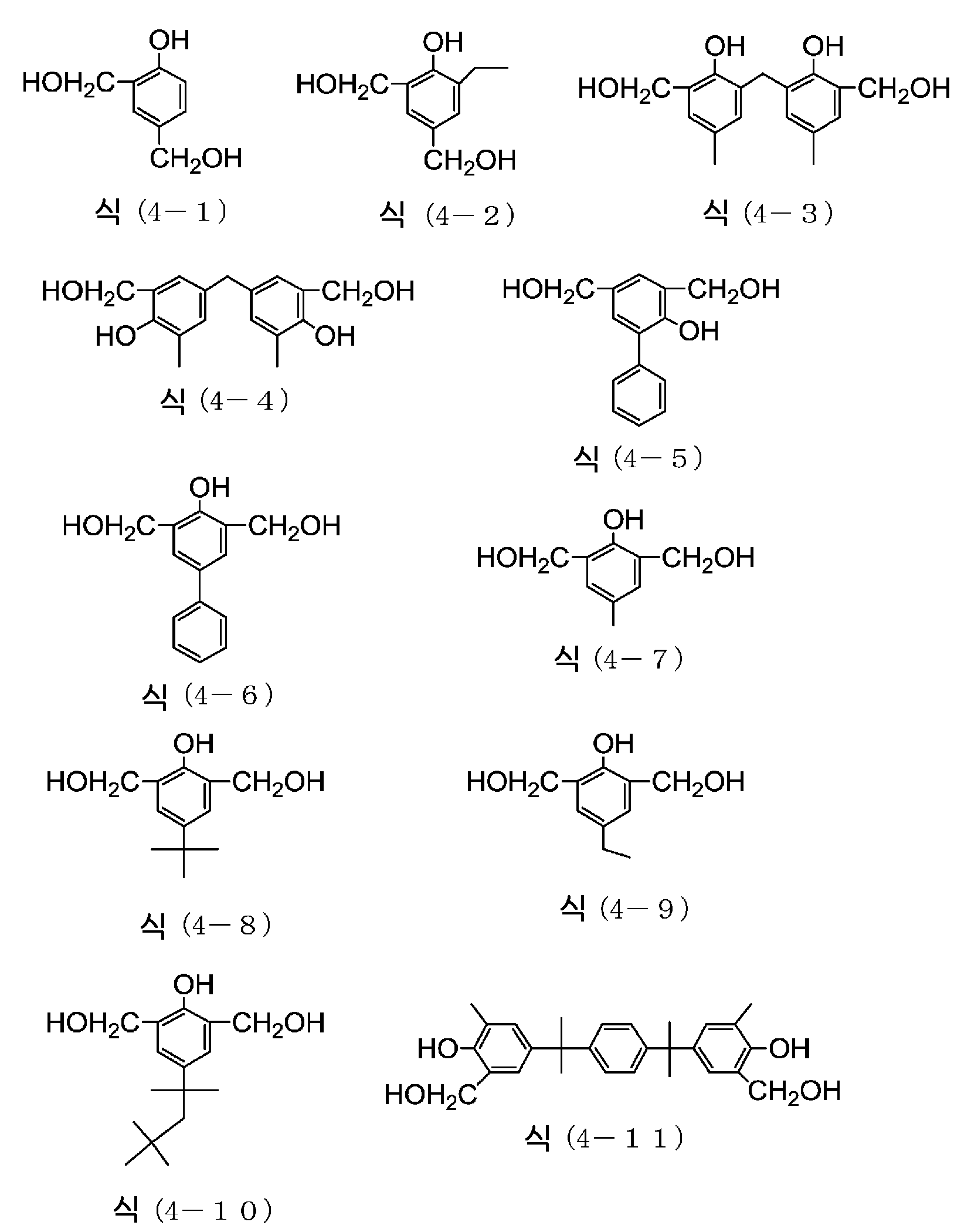
[화학식 8][Formula 8]
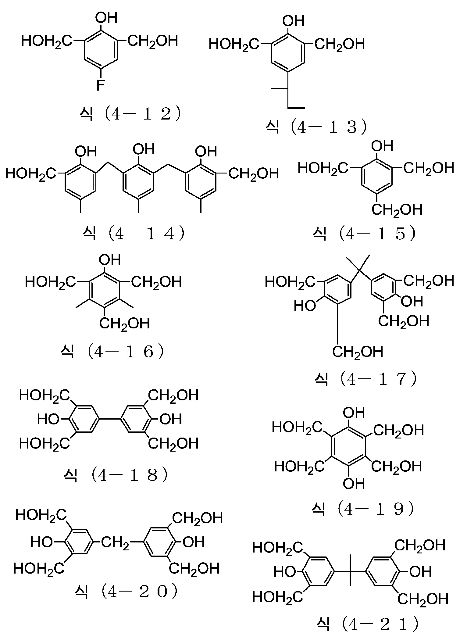
[화학식 9][Formula 9]
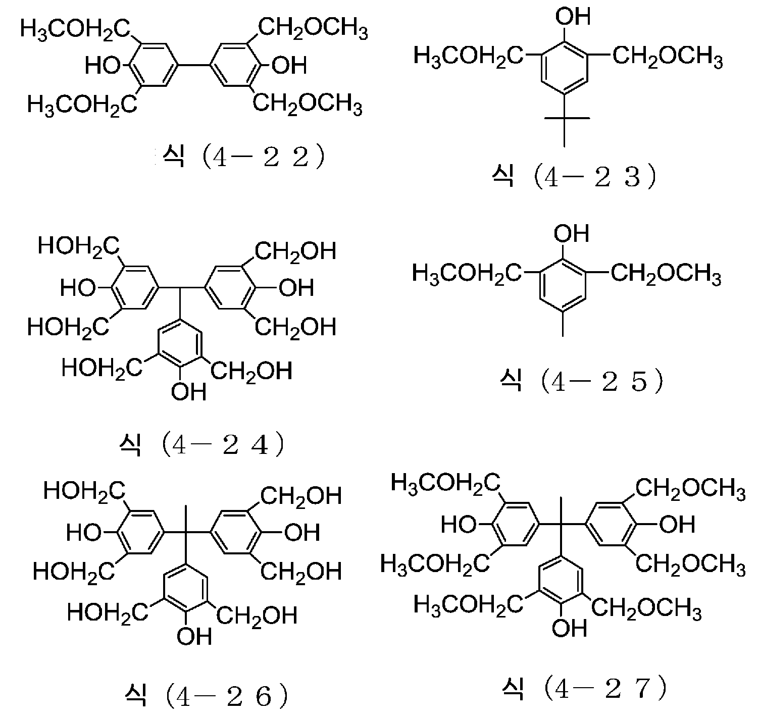
상기 화합물은 Asahi Yukizai Corporation, Honshu Chemical Industry Co.,Ltd.의 제품으로서 입수할 수 있다. 예를 들어 상기 가교제 중에서 식(4-21)로 표시되는 화합물은 Asahi Yukizai Corporation, 상품명 TM-BIP-A로서 입수할 수 있다. 또한, 식(4-22)로 표시되는 화합물은 Honshu Chemical Industry Co.,Ltd., 상품명 TMOM-BP로서 입수할 수 있다.The compound can be obtained as a product of Asahi Yukizai Corporation, Honshu Chemical Industry Co., Ltd. For example, the compound represented by Formula (4-21) among the said crosslinking agents can be obtained as Asahi Yukizai Corporation, brand name TM-BIP-A. In addition, the compound represented by Formula (4-22) can be obtained as Honshu Chemical Industry Co., Ltd., a brand name TMOM-BP.
가교제의 첨가량은, 사용하는 도포용제, 사용하는 하지기판, 요구되는 용액점도, 요구되는 막형상 등에 따라 변동되나, 전체 고형분에 대하여 0.001 내지 80질량%, 바람직하게는 0.01 내지 50질량%, 더욱 바람직하게는 0.05 내지 40질량%이다. 이들 가교제는 자기축합에 의한 가교반응을 일으키는 경우도 있는데, 본 발명의 상기의 폴리머 중에 가교성 치환기가 존재하는 경우는, 이들 가교성 치환기와 가교반응을 일으킬 수 있다.
The amount of the crosslinking agent added varies depending on the coating solvent used, the underlying substrate used, the required solution viscosity, the required film shape, etc., but is 0.001 to 80 mass%, preferably 0.01 to 50 mass%, more preferably based on the total solid content. Preferably it is 0.05-40 mass %. Although these crosslinking agents may cause a crosslinking reaction by self-condensation, when a crosslinkable substituent is present in the polymer of the present invention, it may cause a crosslinking reaction with these crosslinkable substituents.
본 발명에서는 상기 가교반응을 촉진하기 위한 촉매로서, p-톨루엔설폰산, 트리플루오로메탄설폰산, 피리디늄p-톨루엔설폰산, 살리실산, 설포살리실산, 구연산, 안식향산, 하이드록시안식향산, 나프탈렌카르본산 등의 산성 화합물 또는/및 2,4,4,6-테트라브로모시클로헥사디에논, 벤조인토실레이트, 2-니트로벤질토실레이트, 기타 유기설폰산알킬에스테르, 트리플루오로메탄설폰산의 제4급 암모늄염, 등의 열산발생제를 배합할 수 있다. 배합량은 전체 고형분에 대하여, 0.0001 내지 20질량%, 바람직하게는 0.0005 내지 10질량%, 바람직하게는 0.01 내지 3질량%이다.
In the present invention, as a catalyst for promoting the crosslinking reaction, p-toluenesulfonic acid, trifluoromethanesulfonic acid, pyridinium p-toluenesulfonic acid, salicylic acid, sulfosalicylic acid, citric acid, benzoic acid, hydroxybenzoic acid, naphthalenecarboxylic acid Preparation of acidic compounds such as, and/or 2,4,4,6-tetrabromocyclohexadienone, benzointosylate, 2-nitrobenzyltosylate, other organic sulfonic acid alkyl esters, and trifluoromethanesulfonic acid Thermal acid generators, such as a quaternary ammonium salt, can be mix|blended. A compounding quantity is 0.0001-20 mass % with respect to total solid, Preferably it is 0.0005-10 mass %, Preferably it is 0.01-3 mass %.
본 발명의 리소그래피용 레지스트 하층막 형성 조성물은, 리소그래피 공정에서 상층에 피복되는 포토레지스트와의 산성도를 일치시키기 위하여, 광산발생제를 첨가할 수 있다. 바람직한 광산발생제로는, 예를 들어, 비스(4-t-부틸페닐)요오드늄트리플루오로메탄설포네이트, 트리페닐설포늄트리플루오로메탄설포네이트 등의 오늄염계 광산발생제류, 페닐-비스(트리클로로메틸)-s-트리아진 등의 할로겐함유화합물계 광산발생제류, 벤조인토실레이트, N-하이드록시석신이미드트리플루오로메탄설포네이트 등의 설폰산계 광산발생제류 등을 들 수 있다. 상기 광산발생제는 전체 고형분에 대하여, 0.2 내지 10질량%, 바람직하게는0.4 내지 5질량%이다.
In the resist underlayer film forming composition for lithography of the present invention, a photoacid generator may be added in order to match the acidity with the photoresist coated on the upper layer in the lithography process. Preferred photoacid generators include, for example, onium salt-based photoacid generators such as bis(4-t-butylphenyl)iodonium trifluoromethanesulfonate and triphenylsulfonium trifluoromethanesulfonate, phenyl-bis( and halogen-containing compound-based photoacid generators such as trichloromethyl)-s-triazine, and sulfonic acid-based photoacid generators such as benzointosylate and N-hydroxysuccinimide trifluoromethanesulfonate. The said photo-acid generator is 0.2-10 mass % with respect to total solid, Preferably it is 0.4-5 mass %.
본 발명의 리소그래피용 레지스트 하층막재료에는, 상기 이외에 필요에 따라 추가적인 흡광제, 레올로지 조정제, 접착보조제, 계면활성제 등을 첨가할 수 있다.
In addition to the above, additional light absorbers, rheology modifiers, adhesion aids, surfactants, etc. may be added to the resist underlayer film material for lithography of the present invention as needed.
추가적인 흡광제로는 예를 들어, 「공업용 색소의 기술과 시장」(CMC출판)이나 「염료편람」(유기합성화학협회편)에 기재된 시판의 흡광제, 예를 들어, C.I. Disperse Yellow 1, 3, 4, 5, 7, 8, 13, 23, 31, 49, 50, 51, 54, 60, 64, 66, 68, 79, 82, 88, 90, 93, 102, 114 및 124; C.I. Disperse Orange 1, 5, 13, 25, 29, 30, 31, 44, 57, 72 및 73; C.I. Disperse Red 1, 5, 7, 13, 17, 19, 43, 50, 54, 58, 65, 72, 73, 88, 117, 137, 143, 199 및 210; C.I. Disperse Violet 43; C.I. Disperse Blue 96; C.I. Fluorescent Brightening Agent 112, 135 및 163; C.I. Solvent Orange 2 및 45; C.I. Solvent Red 1, 3, 8, 23, 24, 25, 27 및 49; C.I. Pigment Green 10; C.I. Pigment Brown 2 등을 호적하게 이용할 수 있다. 상기 흡광제는 통상, 리소그래피용 레지스트 하층막재료의 전체 고형분에 대하여 10질량% 이하, 바람직하게는 5질량% 이하의 비율로 배합된다.
Additional light absorbers include, for example, commercially available light absorbers described in "Technology and Market of Industrial Dyes" (CMC Publishing) or "Dye Handbook" (Organic Synthetic Chemistry Association edition), for example, CI Disperse Yellow 1, 3, 4, 5, 7, 8, 13, 23, 31, 49, 50, 51, 54, 60, 64, 66, 68, 79, 82, 88, 90, 93, 102, 114 and 124; CI Disperse Orange 1, 5, 13, 25, 29, 30, 31, 44, 57, 72 and 73; CI Disperse Red 1, 5, 7, 13, 17, 19, 43, 50, 54, 58, 65, 72, 73, 88, 117, 137, 143, 199 and 210; CI Disperse Violet 43; CI Disperse Blue 96; CI Fluorescent Brightening Agents 112, 135 and 163; CI Solvent Orange 2 and 45; CI Solvent Red 1, 3, 8, 23, 24, 25, 27 and 49; CI Pigment Green 10; CI Pigment Brown 2 etc. can be used suitably. The light absorber is usually blended in an amount of 10 mass % or less, preferably 5 mass % or less, with respect to the total solid content of the resist underlayer film material for lithography.
레올로지 조정제는, 주로 레지스트 하층막 형성 조성물의 유동성을 향상시키고, 특히 베이킹공정에 있어서, 레지스트 하층막의 막두께균일성의 향상이나 홀 내부로의 레지스트 하층막 형성 조성물의 충전성을 높이는 목적으로 첨가된다. 구체예로는, 디메틸프탈레이트, 디에틸프탈레이트, 디이소부틸프탈레이트, 디헥실프탈레이트, 부틸이소데실프탈레이트 등의 프탈산유도체, 디노말부틸아디페이트, 디이소부틸아디페이트, 디이소옥틸아디페이트, 옥틸데실아디페이트 등의 아디프산유도체, 디노말부틸말레이트, 디에틸말레이트, 디노닐말레이트 등의 말레산유도체, 메틸올레이트, 부틸올레이트, 테트라하이드로푸르푸릴올레이트 등의 올레산유도체, 또는 노말부틸스테아레이트, 글리세릴스테아레이트 등의 스테아르산유도체를 들 수 있다. 이들 레올로지 조정제는, 리소그래피용 레지스트 하층막재료의 전체 고형분에 대하여 통상 30질량% 미만의 비율로 배합된다.
The rheology modifier is mainly added for the purpose of improving the fluidity of the resist underlayer film forming composition, particularly in the baking process, improving the film thickness uniformity of the resist underlayer film and enhancing the filling properties of the resist underlayer film forming composition into the hole. . Specific examples include phthalic acid derivatives such as dimethyl phthalate, diethyl phthalate, diisobutyl phthalate, dihexyl phthalate, butyl isodecyl phthalate, dinormal butyl adipate, diisobutyl adipate, diisooctyl adipate, and octyldecyl. Adipic acid derivatives such as adipate, maleic acid derivatives such as dinormal butyl maleate, diethyl maleate and dinonyl maleate, oleic acid derivatives such as methyl oleate, butyl oleate and tetrahydrofurfuryl oleate, or normal and stearic acid derivatives such as butyl stearate and glyceryl stearate. These rheology modifiers are mix|blended in the ratio of less than 30 mass % normally with respect to the total solid of the resist underlayer film material for lithography.
접착보조제는, 주로 기판 혹은 레지스트와 레지스트 하층막 형성 조성물의 밀착성을 향상시키고, 특히 현상에 있어서 레지스트가 박리되지 않도록 하기 위한 목적으로 첨가된다. 구체예로는, 트리메틸클로로실란, 디메틸비닐클로로실란, 메틸디페닐클로로실란, 클로로메틸디메틸클로로실란 등의 클로로실란류, 트리메틸메톡시실란, 디메틸디에톡시실란, 메틸디메톡시실란, 디메틸비닐에톡시실란, 디페닐디메톡시실란, 페닐트리에톡시실란 등의 알콕시실란류, 헥사메틸디실라잔, N,N'-비스(트리메틸실릴)우레아, 디메틸트리메틸실릴아민, 트리메틸실릴이미다졸 등의 실라잔류, 비닐트리클로로실란, γ-클로로프로필트리메톡시실란, γ-아미노프로필트리에톡시실란, γ-글리시독시프로필트리메톡시실란 등의 실란류, 벤조트리아졸, 벤즈이미다졸, 인다졸, 이미다졸, 2-메르캅토벤즈이미다졸, 2-메르캅토벤조티아졸, 2-메르캅토벤조옥사졸, 우라졸, 티오우라실, 메르캅토이미다졸, 메르캅토피리미딘 등의 복소환식 화합물이나, 1,1-디메틸우레아, 1,3-디메틸우레아 등의 요소, 또는 티오요소 화합물을 들 수 있다. 이들 접착보조제는, 리소그래피용 레지스트 하층막재료의 전체 고형분에 대하여 통상 5질량% 미만, 바람직하게는 2질량% 미만의 비율로 배합된다.
The adhesion auxiliary agent is mainly added for the purpose of improving the adhesion between the substrate or the resist and the resist underlayer film forming composition, and in particular preventing the resist from peeling off during development. Specific examples include chlorosilanes such as trimethylchlorosilane, dimethylvinylchlorosilane, methyldiphenylchlorosilane, and chloromethyldimethylchlorosilane, trimethylmethoxysilane, dimethyldiethoxysilane, methyldimethoxysilane, and dimethylvinylethoxy. Alkoxysilanes such as silane, diphenyldimethoxysilane, and phenyltriethoxysilane, sila such as hexamethyldisilazane, N,N'-bis(trimethylsilyl)urea, dimethyltrimethylsilylamine, and trimethylsilylimidazole Residue, silanes such as vinyltrichlorosilane, γ-chloropropyltrimethoxysilane, γ-aminopropyltriethoxysilane, γ-glycidoxypropyltrimethoxysilane, benzotriazole, benzimidazole, and indazole , imidazole, 2-mercaptobenzimidazole, 2-mercaptobenzothiazole, 2-mercaptobenzooxazole, urazole, thiouracil, mercaptoimidazole, heterocyclic compounds such as mercaptopyrimidine However, urea, such as 1, 1- dimethyl urea and 1, 3- dimethyl urea, or a thiourea compound is mentioned. These adhesion aids are usually blended in an amount of less than 5% by mass, preferably less than 2% by mass based on the total solid content of the resist underlayer film material for lithography.
본 발명의 리소그래피용 레지스트 하층막재료에는, 핀홀이나 스트리에이션 등의 발생이 없고, 표면얼룩에 대한 도포성을 더욱 향상시키기 위하여, 계면활성제를 배합할 수 있다. 계면활성제로는, 예를 들어 폴리옥시에틸렌라우릴에테르, 폴리옥시에틸렌스테아릴에테르, 폴리옥시에틸렌세틸에테르, 폴리옥시에틸렌올레일에테르 등의 폴리옥시에틸렌알킬에테르류, 폴리옥시에틸렌옥틸페놀에테르, 폴리옥시에틸렌노닐페놀에테르 등의 폴리옥시에틸렌알킬알릴에테르류, 폴리옥시에틸렌·폴리옥시프로필렌블록코폴리머류, 솔비탄모노라우레이트, 솔비탄모노팔미테이트, 솔비탄모노스테아레이트, 솔비탄모노올레이트, 솔비탄트리올레이트, 솔비탄트리스테아레이트 등의 솔비탄지방산에스테르류, 폴리옥시에틸렌솔비탄모노라우레이트, 폴리옥시에틸렌솔비탄모노팔미테이트, 폴리옥시에틸렌솔비탄모노스테아레이트, 폴리옥시에틸렌솔비탄트리올레이트, 폴리옥시에틸렌솔비탄트리스테아레이트 등의 폴리옥시에틸렌솔비탄지방산에스테르류 등의 비이온계 계면활성제, EFTOP EF301, EF303, EF352(Tochem Products Co., Ltd.제, 상품명), MEGAFAC F171, F173, R-30, R-30N, R-40LM(Dainippon Ink and Chemicals, Inc.제, 상품명), FLUORAD FC430, FC431(Sumitomo 3M Limited제, 상품명), Asahi Guard AG710, SURFLON S-382, SC101, SC102, SC103, SC104, SC105, SC106(Asahi Glass Co., Ltd.제, 상품명) 등의 불소계 계면활성제, 오가노실록산폴리머 KP341(Shin-Etsu Chemical Co., Ltd.제) 등을 들 수 있다. 이들 계면활성제의 배합량은, 본 발명의 리소그래피용 레지스트 하층막재료의 전체 고형분에 대하여 통상 2.0질량% 이하, 바람직하게는 1.0질량% 이하이다. 이들 계면활성제는 단독으로 첨가할 수도 있고, 또한 2종 이상의 조합으로 첨가할 수도 있다.
In the resist underlayer film material for lithography of the present invention, there is no occurrence of pinholes or striation, and in order to further improve the applicability to surface unevenness, a surfactant can be blended. Examples of the surfactant include polyoxyethylene alkyl ethers such as polyoxyethylene lauryl ether, polyoxyethylene stearyl ether, polyoxyethylene cetyl ether, and polyoxyethylene oleyl ether; polyoxyethylene octyl phenol ether; Polyoxyethylene alkyl allyl ethers such as polyoxyethylene nonyl phenol ether, polyoxyethylene/polyoxypropylene block copolymers, sorbitan monolaurate, sorbitan monopalmitate, sorbitan monostearate, sorbitan monool Sorbitan fatty acid esters such as lactate, sorbitan trioleate, and sorbitan tristearate, polyoxyethylene sorbitan monolaurate, polyoxyethylene sorbitan monopalmitate, polyoxyethylene sorbitan monostearate, and polyoxyethylene sorbitan monostearate. Nonionic surfactants, such as polyoxyethylene sorbitan fatty acid esters such as ethylene sorbitan trioleate and polyoxyethylene sorbitan tristearate, EFTOP EF301, EF303, EF352 (manufactured by Tochem Products Co., Ltd., trade names) ), MEGAFAC F171, F173, R-30, R-30N, R-40LM (manufactured by Dainippon Ink and Chemicals, Inc., trade name), FLUORAD FC430, FC431 (manufactured by Sumitomo 3M Limited, trade name), Asahi Guard AG710, SURFLON S Fluorine surfactants such as -382, SC101, SC102, SC103, SC104, SC105, SC106 (manufactured by Asahi Glass Co., Ltd., trade name), organosiloxane polymer KP341 (manufactured by Shin-Etsu Chemical Co., Ltd.), etc. can be heard The compounding quantity of these surfactant is 2.0 mass % or less normally with respect to the total solid of the resist underlayer film material for lithography of this invention, Preferably it is 1.0 mass % or less. These surfactants may be added alone, or may be added in combination of two or more.
본 발명에서, 상기의 폴리머 및 가교제성분, 가교촉매 등을 용해시키는 용제로는, 에틸렌글리콜모노메틸에테르, 에틸렌글리콜모노에틸에테르, 에틸렌글리콜모노부틸에테르, 에틸렌글리콜모노이소프로필에테르, 에틸렌글리콜메틸에테르아세테이트, 에틸렌글리콜에틸에테르아세테이트, 메틸셀로솔브아세테이트, 에틸셀로솔브아세테이트, 디에틸렌글리콜, 디에틸렌글리콜모노메틸에테르, 디에틸렌글리콜모노에틸에테르, 디에틸렌글리콜디메틸에테르, 디에틸렌글리콜디에틸에테르, 디에틸렌글리콜모노에틸에테르아세테이트, 프로필렌글리콜, 프로필렌글리콜모노메틸에테르, 프로필렌글리콜모노부틸에테르, 프로필렌글리콜모노메틸에테르아세테이트, 프로필렌글리콜모노에틸에테르, 프로필렌글리콜모노에틸에테르아세테이트, 프로필렌글리콜프로필에테르아세테이트, 디프로필렌글리콜모노메틸에테르, 디프로필렌글리콜모노에틸에테르, 트리에틸렌글리콜디메틸에테르, 톨루엔, 자일렌, 스티렌, 메틸에틸케톤, 시클로펜탄온, 시클로헥사논, 2-하이드록시프로피온산에틸, 2-하이드록시-2-메틸프로피온산에틸, 에톡시아세트산에틸, 하이드록시아세트산에틸, 2-하이드록시-3-메틸부탄산메틸, 3-메톡시프로피온산메틸, 3-메톡시프로피온산에틸, 3-에톡시프로피온산에틸, 3-에톡시프로피온산메틸, 피루브산메틸, 피루브산에틸, 아세트산에틸, 아세트산부틸, 유산에틸, 유산부틸, 1-옥탄올, 에틸렌글리콜, 헥실렌글리콜, 트리메틸렌글리콜, 1-메톡시-2-부탄올, 시클로헥산올, 디아세톤알코올, 푸르푸릴알코올, 테트라하이드로푸르푸릴알코올, 프로필렌글리콜, 벤질알코올, 1,3-부탄디올, 1,4-부탄디올, 2,3-부탄디올, γ-부틸락톤, 아세톤, 메틸이소프로필케톤, 디에틸케톤, 메틸이소부틸케톤, 메틸노말부틸케톤, 아세트산이소프로필케톤, 아세트산노말프로필, 아세트산이소부틸, 메탄올, 에탄올, 이소프로판올, tert-부탄올, 알릴알코올, 노말프로판올, 2-메틸-2-부탄올, 이소부탄올, 노말부탄올, 2-메틸-1-부탄올, 1-펜탄올, 2-메틸-1-펜탄올, 2-에틸헥산올, 1-옥탄올, 에틸렌글리콜, 헥실렌글리콜, 트리메틸렌글리콜, 1-메톡시-2-부탄올, 디아세톤알코올, 푸르푸릴알코올, 테트라하이드로푸르푸릴알코올, 프로필렌글리콜, 벤질알코올, 이소프로필에테르, 1,4-디옥산, N,N-디메틸포름아미드, N,N-디메틸아세트아미드, N-메틸피롤리돈, 1,3-디메틸-2-이미다졸리디논, 디메틸설폭사이드, N-시클로헥실-2-피롤리디논 등을 이용할 수 있다. 이들 유기용제는 단독으로, 또는 2종 이상의 조합으로 사용된다.In the present invention, as a solvent for dissolving the polymer, crosslinking agent component, crosslinking catalyst, etc., ethylene glycol monomethyl ether, ethylene glycol monoethyl ether, ethylene glycol monobutyl ether, ethylene glycol monoisopropyl ether, ethylene glycol methyl ether, etc. Acetate, ethylene glycol ethyl ether acetate, methyl cellosolve acetate, ethyl cellosolve acetate, diethylene glycol, diethylene glycol monomethyl ether, diethylene glycol monoethyl ether, diethylene glycol dimethyl ether, diethylene glycol diethyl ether , Diethylene glycol monoethyl ether acetate, propylene glycol, propylene glycol monomethyl ether, propylene glycol monobutyl ether, propylene glycol monomethyl ether acetate, propylene glycol monoethyl ether, propylene glycol monoethyl ether acetate, propylene glycol propyl ether acetate, Dipropylene glycol monomethyl ether, dipropylene glycol monoethyl ether, triethylene glycol dimethyl ether, toluene, xylene, styrene, methyl ethyl ketone, cyclopentanone, cyclohexanone, 2-hydroxyethyl propionate, 2-hydroxy -2-methylpropionate, ethyl ethoxyacetate, ethyl hydroxyacetate, methyl 2-hydroxy-3-methylbutanoate, methyl 3-methoxypropionate, ethyl 3-methoxypropionate, ethyl 3-ethoxypropionate, 3-ethoxy methyl propionate, methyl pyruvate, ethyl pyruvate, ethyl acetate, butyl acetate, ethyl lactate, butyl lactate, 1-octanol, ethylene glycol, hexylene glycol, trimethylene glycol, 1-methoxy-2-butanol, Cyclohexanol, diacetone alcohol, furfuryl alcohol, tetrahydrofurfuryl alcohol, propylene glycol, benzyl alcohol, 1,3-butanediol, 1,4-butanediol, 2,3-butanediol, γ-butyllactone, acetone, methyl Isopropyl ketone, diethyl ketone, methyl isobutyl ketone, methyl normal butyl ketone, isopropyl ketone acetate, normal propyl acetate, isobutyl acetate, methanol, ethanol, isopropanol, tert-butanol, allyl alcohol, normal propanol, 2-methyl -2-butanol, isobutanol, n-butanol, 2-methyl-1-butanol, 1-pentanol, 2-methyl-1-pentanol, 2-ethylhexanol, 1-octanol, ethylene glycol, hexylene glycol , Trimethylene glycol, 1-methoxy-2-butanol, diacetone alcohol, furfuryl alcohol, tetrahydrofurfuryl alcohol, propylene glycol, benzyl alcohol, isopropyl ether, 1,4-dioxane, N,N-dimethylform Amide, N,N-dimethylacetamide, N-methylpyrrolidone, 1,3-dimethyl-2-imidazolidinone, dimethyl sulfoxide, N-cyclohexyl-2-pyrrolidinone and the like can be used. These organic solvents are used individually or in combination of 2 or more types.
나아가, 프로필렌글리콜모노부틸에테르, 프로필렌글리콜모노부틸에테르아세테이트 등의 고비점용제를 혼합하여 사용할 수 있다. 이들 용제 중에서 프로필렌글리콜모노메틸에테르, 프로필렌글리콜모노메틸에테르아세테이트, 프로필렌글리콜모노부틸에테르, 유산에틸, 유산부틸, 및 시클로헥사논 등이 레벨링성의 향상에 대하여 바람직하다.
Furthermore, high boiling point solvents, such as propylene glycol monobutyl ether and propylene glycol monobutyl ether acetate, can be mixed and used. Among these solvents, propylene glycol monomethyl ether, propylene glycol monomethyl ether acetate, propylene glycol monobutyl ether, ethyl lactate, butyl lactate, cyclohexanone and the like are preferable for improving leveling properties.
본 발명에 이용되는 레지스트란 포토레지스트나 전자선 레지스트이다.The resist used in the present invention is a photoresist or an electron beam resist.
본 발명에 있어서의 리소그래피용 레지스트 하층막의 상부에 도포되는 포토레지스트로는 네가티브형, 포지티브형 모두 사용할 수 있고, 노볼락수지와 1,2-나프토퀴논디아지드설폰산에스테르로 이루어진 포지티브형 포토레지스트, 산에 의해 분해되어 알칼리용해속도를 상승시키는 기를 갖는 바인더와 광산발생제로 이루어진 화학증폭형 포토레지스트, 알칼리가용성 바인더와 산에 의해 분해되어 포토레지스트의 알칼리용해속도를 상승시키는 저분자 화합물과 광산발생제로 이루어진 화학증폭형 포토레지스트, 산에 의해 분해되어 알칼리용해속도를 상승시키는 기를 갖는 바인더와 산에 의해 분해되어 포토레지스트의 알칼리용해속도를 상승시키는 저분자 화합물과 광산발생제로 이루어진 화학증폭형 포토레지스트, 골격에 Si원자를 갖는 포토레지스트 등이 있고, 예를 들어, Rohm and Haas Electronic Materials K.K.제, 상품명 APEX-E를 들 수 있다.
As the photoresist applied to the upper portion of the resist underlayer for lithography in the present invention, both a negative type and a positive type may be used, and a positive type photoresist composed of a novolak resin and 1,2-naphthoquinonediazidesulfonic acid ester. , chemically amplified photoresist consisting of a binder and a photoacid generator having a group that is decomposed by acid to increase the alkali dissolution rate, a low molecular weight compound that is decomposed by an alkali-soluble binder and acid to increase the alkali dissolution rate of the photoresist, and a photoacid generator Chemically amplified photoresist consisting of a chemically amplified photoresist consisting of a binder having a group that increases the alkali dissolution rate by decomposition by acid, a low molecular weight compound and a photoacid generator that is decomposed by acid to increase the alkali dissolution rate of the photoresist, a skeleton There exist a photoresist etc. which have Si atoms, for example, the product made from Rohm and Haas Electronic Materials KK, brand name APEX-E is mentioned.
또한 본 발명에 있어서의 리소그래피용 레지스트 하층막의 상부에 도포되는 전자선 레지스트로는, 예를 들어 주쇄에 Si-Si결합을 포함하고 말단에 방향족환을 포함한 수지와 전자선의 조사에 의해 산을 발생시키는 산발생제로 이루어진 조성물, 또는 하이드록시기가 N-카르복시아민을 포함한 유기기로 치환된 폴리(p-하이드록시스티렌)과 전자선의 조사에 의해 산을 발생시키는 산발생제로 이루어진 조성물 등을 들 수 있다. 후자의 전자선 레지스트 조성물에서는, 전자선 조사에 의해 산발생제로부터 발생한 산이 폴리머측쇄의 N-카르복시아미녹시기와 반응하고, 폴리머측쇄가 하이드록시기에 분해되어 알칼리가용성을 나타내고 알칼리현상액에 용해되고, 레지스트패턴을 형성하는 것이다. 이 전자선의 조사에 의해 산을 발생시키는 산발생제는 1,1-비스[p-클로로페닐]-2,2,2-트리클로로에탄, 1,1-비스[p-메톡시페닐]-2,2,2-트리클로로에탄, 1,1-비스[p-클로로페닐]-2,2-디클로로에탄, 2-클로로-6-(트리클로로메틸)피리딘 등의 할로겐화유기화합물, 트리페닐설포늄염, 디페닐요오드늄염 등의 오늄염, 니트로벤질토실레이트, 디니트로벤질토실레이트 등의 설폰산에스테르를 들 수 있다.
In the present invention, as the electron beam resist applied to the upper portion of the resist underlayer film for lithography, for example, a resin containing a Si-Si bond in the main chain and an aromatic ring at the terminal thereof, and an acid generating acid upon irradiation with an electron beam and a composition comprising a generator or poly(p-hydroxystyrene) in which a hydroxyl group is substituted with an organic group including N-carboxyamine, and a composition comprising an acid generator that generates an acid upon irradiation with an electron beam. In the latter electron beam resist composition, the acid generated from the acid generator by electron beam irradiation reacts with the N-carboxyamino group of the polymer side chain, and the polymer side chain is decomposed to a hydroxyl group to exhibit alkali solubility and dissolve in an alkali developer, and the resist to form a pattern. The acid generator that generates an acid by irradiation with this electron beam is 1,1-bis[p-chlorophenyl]-2,2,2-trichloroethane, 1,1-bis[p-methoxyphenyl]-2 Halogenated organic compounds such as ,2,2-trichloroethane, 1,1-bis[p-chlorophenyl]-2,2-dichloroethane, 2-chloro-6-(trichloromethyl)pyridine, triphenylsulfonium salt and onium salts such as diphenyliodonium salt, sulfonic acid esters such as nitrobenzyltosylate and dinitrobenzyltosylate.
본 발명의 리소그래피용 레지스트 하층막재료를 사용하여 형성한 레지스트 하층막을 갖는 레지스트의 현상액으로는, 수산화나트륨, 수산화칼륨, 탄산나트륨, 규산나트륨, 메타규산나트륨, 암모니아수 등의 무기알칼리류, 에틸아민, n-프로필아민 등의 제1 아민류, 디에틸아민, 디-n-부틸아민 등의 제2 아민류, 트리에틸아민, 메틸디에틸아민 등의 제3 아민류, 디메틸에탄올아민, 트리에탄올아민 등의 알코올아민류, 테트라메틸암모늄하이드록시드, 테트라에틸암모늄하이드록시드, 콜린 등의 제4급 암모늄염, 피롤, 피페리딘 등의 환상아민류, 등의 알칼리류의 수용액을 사용할 수 있다. 나아가, 상기 알칼리류의 수용액에 이소프로필알코올 등의 알코올류, 비이온계 등의 계면활성제를 적당량 첨가하여 사용할 수도 있다. 이들 중에서 바람직한 현상액은 제4급 암모늄염, 더욱 바람직하게는 테트라메틸암모늄하이드록시드 및 콜린이다.
As a developer solution for a resist having a resist underlayer film formed using the resist underlayer film material for lithography of the present invention, inorganic alkalis such as sodium hydroxide, potassium hydroxide, sodium carbonate, sodium silicate, sodium metasilicate, aqueous ammonia, ethylamine, n - Primary amines such as propylamine, secondary amines such as diethylamine and di-n-butylamine, tertiary amines such as triethylamine and methyldiethylamine, alcohol amines such as dimethylethanolamine and triethanolamine; Aqueous solutions of alkalis, such as quaternary ammonium salts, such as tetramethylammonium hydroxide, tetraethylammonium hydroxide, and choline, cyclic amines, such as pyrrole and piperidine, can be used. Furthermore, an appropriate amount of an alcohol such as isopropyl alcohol or a surfactant such as a nonionic surfactant may be added to the aqueous alkali solution. Among these, preferred developing solutions are quaternary ammonium salts, more preferably tetramethylammonium hydroxide and choline.
이어서 본 발명의 레지스트 패턴 형성법에 대하여 설명하면, 정밀집적 회로소자의 제조에 사용되는 기판(예를 들어 실리콘/이산화실리콘피복, 유리기판, ITO기판 등의 투명기판) 상에 스피너, 코터 등의 적당한 도포방법에 의해 레지스트 하층막 형성 조성물을 도포 후, 베이크하여 경화시켜 도포형 하층막을 작성한다. 여기서, 레지스트 하층막의 막두께로는 0.01 내지 3.0μm가 바람직하다. 또한 도포후 베이킹하는 조건으로는 80 내지 350℃에서 0.5 내지 120분간이다. 그 후 레지스트 하층막 상에 직접, 또는 필요에 따라 1층 내지 수층의 도막재료를 도포형 하층막 상에 성막한 후, 레지스트를 도포하고, 소정의 마스크를 통과하여 광 또는 전자선의 조사를 행하고, 현상, 린스, 건조함으로써 양호한 레지스트패턴을 얻을 수 있다. 필요에 따라 광 또는 전자선의 조사후 가열(PEB: Post Exposure Bake)을 행할 수도 있다. 그리고, 레지스트가 상기 공정에 의해 현상제거된 부분의 레지스트 하층막을 드라이에칭에 의해 제거하고, 원하는 패턴을 기판 상에 형성할 수 있다.
Next, the resist pattern formation method of the present invention will be described, on a substrate used for manufacturing a precision integrated circuit device (for example, a transparent substrate such as silicon/silicon dioxide coating, glass substrate, ITO substrate), a spinner, a coater, etc. After the resist underlayer film forming composition is applied by the coating method, it is baked and cured to prepare a coating type underlayer film. Here, as a film thickness of a resist underlayer film, 0.01-3.0 micrometers is preferable. In addition, the conditions for baking after application are 0.5 to 120 minutes at 80 to 350°C. After that, directly on the resist underlayer, or if necessary, one to several layers of a coating material are formed on the application-type underlayer, then the resist is applied, and light or electron beams are irradiated through a predetermined mask, A good resist pattern can be obtained by developing, rinsing and drying. Heating after irradiation of light or an electron beam (PEB:Post Exposure Bake) can also be performed as needed. Then, the resist underlayer film in the portion where the resist is developed and removed by the above process is removed by dry etching, and a desired pattern can be formed on the substrate.
상기 포토레지스트에서의 노광광은, 근자외선, 원자외선, 또는 극단자외선(예를 들어, EUV, 파장 13.5nm) 등의 화학선이며, 예를 들어 248nm(KrF레이저광), 193nm(ArF레이저광), 157nm(F2레이저광) 등의 파장의 광이 이용된다. 광조사에는, 광산발생제로부터 산을 발생시킬 수 있는 방법이면, 특별히 제한 없이 사용할 수 있고, 노광량 1 내지 2000mJ/cm2, 또는 10 내지 1500mJ/cm2, 또는 50 내지 1000mJ/cm2에 따른다.
The exposure light in the photoresist is actinic radiation such as near ultraviolet, far ultraviolet, or extreme ultraviolet (eg, EUV, wavelength 13.5 nm), for example, 248 nm (KrF laser light), 193 nm (ArF laser light). ), light having a wavelength such as 157 nm (F 2 laser light) is used. In the light irradiation, is a method capable of generating an acid from a photo-acid generating agent, it can be used without particular limitation, be in accordance with the exposure amount of 1 to 2000mJ / cm 2, or 10 to 1500mJ / cm 2, or 50 to 1000mJ / cm 2.
또한 전자선 레지스트의 전자선 조사는, 예를 들어 전자선 조사장치를 이용하여 조사할 수 있다.In addition, electron beam irradiation of an electron beam resist can be irradiated using an electron beam irradiation apparatus, for example.
본 발명에서는, 반도체기판 상에 본 발명의 레지스트 하층막 형성 조성물에 의해 이 레지스트 하층막을 형성하는 공정, 그 위에 레지스트막을 형성하는 공정, 광 또는 전자선 조사와 현상에 의해 레지스트패턴을 형성하는 공정, 형성된 레지스트패턴에 의해 이 레지스트 하층막을 에칭하는 공정, 및 패턴화된 레지스트 하층막에 의해 반도체기판을 가공하는 공정을 거쳐 반도체장치를 제조할 수 있다.
In the present invention, a step of forming the resist underlayer film on a semiconductor substrate with the resist underlayer film forming composition of the present invention, a step of forming a resist film thereon, a step of forming a resist pattern by light or electron beam irradiation and development, the formed A semiconductor device can be manufactured through the process of etching this resist underlayer film with a resist pattern, and processing a semiconductor substrate with the patterned resist underlayer film.
향후, 레지스트패턴의 미세화가 진행되면, 해상도의 문제나 레지스트패턴이 현상 후에 무너진다는 문제가 생겨, 레지스트의 박막화가 요구되고 있다. 이에 따라, 기판가공에 충분한 레지스트패턴 막두께를 얻는 것이 어렵고, 레지스트패턴뿐만 아니라, 레지스트와 가공하는 반도체기판의 사이에 작성되는 레지스트 하층막에도 기판가공시의 마스크로서의 기능을 갖게 하는 프로세스가 필요하게 되었다. 이러한 프로세스용 레지스트 하층막으로서 종래의 고에칭레이트성 레지스트 하층막과는 달리, 레지스트에 가까운 드라이에칭속도의 선택비를 갖는 리소그래피용 레지스트 하층막, 레지스트에 비해 작은 드라이에칭속도의 선택비를 갖는 리소그래피용 레지스트 하층막이나 반도체기판에 비해 작은 드라이에칭속도의 선택비를 갖는 리소그래피용 레지스트 하층막이 요구되고 있다. 또한, 이러한 레지스트 하층막에는 반사방지능을 부여하는 것도 가능하며, 종래의 반사방지막의 기능을 겸비할 수 있다.
In the future, if the resist pattern is miniaturized, a problem of resolution and a problem that the resist pattern collapses after development arises, and thinning of the resist is required. Accordingly, it is difficult to obtain a resist pattern film thickness sufficient for substrate processing, and a process is required for not only the resist pattern but also the resist underlayer film created between the resist and the semiconductor substrate to be processed to function as a mask during substrate processing. became As a resist underlayer film for this process, unlike the conventional high etching rate resist underlayer film, the resist underlayer film for lithography has a selectivity of a dry etching rate close to that of resist, and lithography having a selectivity of a dry etching rate smaller than that of resist. There is a demand for a resist underlayer film for lithography, which has a selectivity ratio of a dry etching rate smaller than that of a resist underlayer film or a semiconductor substrate. In addition, it is possible to impart antireflection ability to such a resist underlayer film, and it is possible to combine the functions of a conventional antireflection film.
한편, 미세한 레지스트패턴을 얻기 위하여, 레지스트 하층막의 드라이에칭시에 레지스트패턴과 레지스트 하층막을 레지스트현상시의 패턴폭보다 얇게 하는 프로세스도 사용되기 시작하고 있다. 이러한 프로세스용 레지스트 하층막으로서 종래의 고에칭레이트성 반사방지막과는 달리, 레지스트에 가까운 드라이에칭속도의 선택비를 갖는 레지스트 하층막이 요구되고 있다. 또한, 이러한 레지스트 하층막에는 반사방지능을 부여하는 것도 가능하며, 종래의 반사방지막의 기능을 겸비할 수 있다.
On the other hand, in order to obtain a fine resist pattern, a process of making the resist pattern and the resist underlayer film thinner than the pattern width at the time of resist development during dry etching of the resist underlayer film is also beginning to be used. As a resist underlayer film for such a process, a resist underlayer film having a selectivity ratio of a dry etching rate close to that of a resist is required, unlike the conventional high etching rate antireflection film. In addition, it is possible to impart antireflection ability to such a resist underlayer film, and it is possible to combine the functions of a conventional antireflection film.
본 발명에서는 기판 상에 본 발명의 레지스트 하층막을 성막한 후, 레지스트 하층막 상에 직접, 또는 필요에 따라 1층 내지 수층의 도막재료를 레지스트 하층막 상에 성막한 후, 레지스트를 도포할 수 있다. 이에 따라 레지스트의 패턴폭이 좁아지고, 패턴무너짐을 방지하기 위하여 레지스트를 얇게 피복한 경우에도, 적절한 에칭가스를 선택함으로써 기판의 가공이 가능해진다.
In the present invention, after the resist underlayer film of the present invention is formed on the substrate, the resist can be applied directly on the resist underlayer film or after forming one to several layers of coating material on the resist underlayer film as needed. . Accordingly, the pattern width of the resist becomes narrow, and even when the resist is thinly coated to prevent pattern collapse, processing of the substrate becomes possible by selecting an appropriate etching gas.
즉, 반도체기판 상에 본 발명의 레지스트 하층막 형성 조성물에 의해 이 레지스트 하층막을 형성하는 공정, 그 위에 규소성분 등을 함유하는 도막재료에 의한 하드마스크 또는 증착에 의한 하드마스크(예를 들어, 질화산화규소)를 형성하는 공정, 추가로 그 위에 레지스트막을 형성하는 공정, 광 또는 전자선의 조사와 현상에 의해 레지스트패턴을 형성하는 공정, 형성된 레지스트패턴에 의해 하드마스크를 할로겐계 가스로 에칭하는 공정, 패턴화된 하드마스크에 의해 이 레지스트 하층막을 산소계 가스 또는 수소계 가스로 에칭하는 공정, 및 패턴화된 레지스트 하층막에 의해 할로겐계 가스로 반도체기판을 가공하는 공정을 거쳐 반도체장치를 제조할 수 있다.
That is, a step of forming the resist underlayer film on a semiconductor substrate with the resist underlayer film forming composition of the present invention, a hard mask using a coating film material containing a silicon component thereon, or a hard mask by vapor deposition (e.g., nitriding) silicon oxide), further forming a resist film thereon; A semiconductor device can be manufactured through a process of etching the resist underlayer film with an oxygen-based gas or a hydrogen-based gas using a patterned hard mask, and processing a semiconductor substrate with a halogen-based gas using the patterned resist underlayer film. .
본 발명의 리소그래피용 레지스트 하층막 형성 조성물은, 반사방지막으로서의 효과를 고려한 경우, 광흡수부위가 골격에 취입되므로, 가열건조시에 포토레지스트 중으로의 확산물이 없고, 또한, 광흡수부위는 충분히 큰 흡광성능을 갖고 있으므로 반사광 방지효과가 높다.
In the resist underlayer film forming composition for lithography of the present invention, when the effect as an antireflection film is considered, the light absorbing site is blown into the skeleton, so there is no diffusion into the photoresist during heating and drying, and the light absorbing site is sufficiently large Because it has light absorption performance, it has a high anti-reflection effect.
본 발명의 리소그래피용 레지스트 하층막 형성 조성물에서는, 열안정성이 높고, 소성시의 분해물에 의한 상층막에 대한 오염이 방지되고, 또한, 소성공정의 온도마진에 여유를 가질 수 있는 것이다.
In the resist underlayer film forming composition for lithography of the present invention, thermal stability is high, contamination of the upper layer film by decomposition products during firing is prevented, and a temperature margin in the firing process can be afforded.
나아가, 본 발명의 리소그래피용 레지스트 하층막재료는, 프로세스 조건에 따라서는, 광의 반사를 방지하는 기능과, 더 나아가 기판과 포토레지스트의 상호작용의 방지 혹은 포토레지스트에 이용되는 재료 또는 포토레지스트에 대한 노광시에 생성되는 물질의 기판에 대한 악작용을 방지하는 기능을 갖는 막으로서의 사용이 가능하다.
Furthermore, the resist underlayer film material for lithography of the present invention has a function of preventing reflection of light, furthermore, preventing interaction between a substrate and a photoresist, or a material or photoresist used for a photoresist depending on process conditions. It can be used as a film having a function of preventing an adverse action on a substrate of a material generated during exposure.
실시예Example
합성예 1Synthesis Example 1
100mL 4구 플라스크에 N-메틸아닐린(4.50g, 0.042mol, Tokyo Chemical Industry Co., Ltd.제), 1-나프토알데히드(6.56g, 0.042mol, Tokyo Chemical Industry Co., Ltd.제), 메탄설폰산(1.21g, 0.0126mol, Kanto Chemical Co., Inc.제)을 첨가하고, 프로필렌글리콜모노메틸에테르(18.41g, Kanto Chemical Co., Inc.제)를 투입 교반하고, 120℃까지 승온하여 용해시켜 중합을 개시하였다. 30시간 후 실온까지 방랭 후, 메탄올(800g, Kanto Chemical Co., Inc.제)에 재침전시켰다. 얻어진 침전물을 여과하고, 감압건조기로 80℃, 10시간 건조하여, 목적으로 하는 폴리머(식(2-2), 이하 PMA-NA라 약칭함) 4.2g을 얻었다.In a 100 mL four-necked flask, N-methylaniline (4.50 g, 0.042 mol, manufactured by Tokyo Chemical Industry Co., Ltd.), 1-naphthoaldehyde (6.56 g, 0.042 mol, manufactured by Tokyo Chemical Industry Co., Ltd.), Methanesulfonic acid (1.21 g, 0.0126 mol, manufactured by Kanto Chemical Co., Inc.) was added, propylene glycol monomethyl ether (18.41 g, manufactured by Kanto Chemical Co., Inc.) was added and stirred, and the temperature was raised to 120°C. was dissolved to initiate polymerization. After standing to cool to room temperature after 30 hours, it was reprecipitated in methanol (800 g, manufactured by Kanto Chemical Co., Inc.). The resulting precipitate was filtered and dried at 80°C for 10 hours in a vacuum dryer to obtain 4.2 g of the target polymer (formula (2-2), hereinafter abbreviated as PMA-NA).
PMA-NA의 GPC에 의한 폴리스티렌 환산으로 측정되는 중량평균 분자량Mw은 1800, 다분산도Mw/Mn는 1.48이었다.
The weight average molecular weight Mw measured in terms of polystyrene by GPC of PMA-NA was 1800, and the polydispersity Mw/Mn was 1.48.
합성예 2Synthesis Example 2
100mL 4구 플라스크에 N-메틸아닐린(3.50g, 0.033mol, Tokyo Chemical Industry Co., Ltd.제), 1-피렌카르복시알데히드(7.52g, 0.033mol, Tokyo Chemical Industry Co., Ltd.제), 메탄설폰산(0.94g, 0.0098mol, Kanto Chemical Co., Inc.제)을 첨가하고, 프로필렌글리콜모노메틸에테르(17.95g, Kanto Chemical Co., Inc.제)를 투입 교반하고, 120℃까지 승온하여 용해시켜 중합을 개시하였다. 30시간 후 실온까지 방랭 후, 메탄올(800g, Kanto Chemical Co., Inc.제)에 재침전시켰다. 얻어진 침전물을 여과하고, 감압건조기로 80℃, 10시간 건조하여, 목적으로 하는 폴리머(식(2-7), 이하 PMA-PcA라 약칭함) 7.6g을 얻었다.In a 100 mL four-necked flask, N-methylaniline (3.50 g, 0.033 mol, manufactured by Tokyo Chemical Industry Co., Ltd.), 1-pyrenecarboxyaldehyde (7.52 g, 0.033 mol, manufactured by Tokyo Chemical Industry Co., Ltd.), Methanesulfonic acid (0.94 g, 0.0098 mol, manufactured by Kanto Chemical Co., Inc.) was added, propylene glycol monomethyl ether (17.95 g, manufactured by Kanto Chemical Co., Inc.) was added and stirred, and the temperature was raised to 120°C. was dissolved to initiate polymerization. After standing to cool to room temperature after 30 hours, it was reprecipitated in methanol (800 g, manufactured by Kanto Chemical Co., Inc.). The resulting precipitate was filtered and dried at 80° C. for 10 hours with a vacuum dryer to obtain 7.6 g of the target polymer (formula (2-7), hereinafter abbreviated as PMA-PcA).
PMA-PcA의 GPC에 의한 폴리스티렌 환산으로 측정되는 중량평균 분자량Mw은 1100, 다분산도Mw/Mn는 1.43이었다.
The weight average molecular weight Mw measured in terms of polystyrene by GPC of PMA-PcA was 1100, and the polydispersity Mw/Mn was 1.43.
합성예 3Synthesis Example 3
100mL 4구 플라스크에 N-벤질아닐린(8.00g, 0.044mol, Tokyo Chemical Industry Co., Ltd.제), 1-나프토알데히드(6.82g, 0.044mol, Tokyo Chemical Industry Co., Ltd.제), 메탄설폰산(1.26g, 0.0131mol, Kanto Chemical Co., Inc.제)을 첨가하고, 프로필렌글리콜모노메틸에테르아세테이트(24.12g, Kanto Chemical Co., Inc.제)를 투입 교반하고, 120℃까지 승온하여 용해시켜 중합을 개시하였다. 30시간 후 실온까지 방랭 후, 메탄올(800g, Kanto Chemical Co., Inc.제)에 재침전시켰다. 얻어진 침전물을 여과하고, 감압건조기로 80℃, 10시간 건조하여, 목적으로 하는 폴리머(식(3-2), 이하 PPBA-NA라 약칭함) 6.8g을 얻었다.In a 100 mL four-necked flask, N-benzylaniline (8.00 g, 0.044 mol, manufactured by Tokyo Chemical Industry Co., Ltd.), 1-naphthoaldehyde (6.82 g, 0.044 mol, manufactured by Tokyo Chemical Industry Co., Ltd.), Methanesulfonic acid (1.26 g, 0.0131 mol, manufactured by Kanto Chemical Co., Inc.) was added, propylene glycol monomethyl ether acetate (24.12 g, manufactured by Kanto Chemical Co., Inc.) was added and stirred, and the mixture was stirred until 120°C. Polymerization was initiated by dissolution by raising the temperature. After standing to cool to room temperature after 30 hours, it was reprecipitated in methanol (800 g, manufactured by Kanto Chemical Co., Inc.). The resulting precipitate was filtered and dried at 80° C. for 10 hours with a vacuum dryer to obtain 6.8 g of the target polymer (formula (3-2), hereinafter abbreviated as PPBA-NA).
PPBA-NA의 GPC에 의한 폴리스티렌 환산으로 측정되는 중량평균 분자량Mw은 1400, 다분산도Mw/Mn는 1.25였다.
The weight average molecular weight Mw measured in terms of polystyrene by GPC of PPBA-NA was 1400, and the polydispersity Mw/Mn was 1.25.
합성예 4Synthesis Example 4
100mL 4구 플라스크에 N-벤질아닐린(8.00g, 0.044mol, Tokyo Chemical Industry Co., Ltd.제), 1-피렌카르복시알데히드(10.05g, 0.044mol, Tokyo Chemical Industry Co., Ltd.제), 메탄설폰산(1.26g, 0.0131mol, Kanto Chemical Co., Inc.제)을 첨가하고, 프로필렌글리콜모노메틸에테르아세테이트(28.97g, Kanto Chemical Co., Inc.제)를 투입 교반하고, 120℃까지 승온하여 용해시켜 중합을 개시하였다. 30시간 후 실온까지 방랭 후, 메탄올(800g, Kanto Chemical Co., Inc.제)에 재침전시켰다. 얻어진 침전물을 여과하고, 감압건조기로 80℃, 10시간 건조하여, 목적으로 하는 폴리머(식(3-7), 이하 PPBA-PcA라 약칭함) 10.8g을 얻었다.In a 100 mL four-neck flask, N-benzylaniline (8.00 g, 0.044 mol, manufactured by Tokyo Chemical Industry Co., Ltd.), 1-pyrenecarboxyaldehyde (10.05 g, 0.044 mol, manufactured by Tokyo Chemical Industry Co., Ltd.), Methanesulfonic acid (1.26 g, 0.0131 mol, manufactured by Kanto Chemical Co., Inc.) was added, propylene glycol monomethyl ether acetate (28.97 g, manufactured by Kanto Chemical Co., Inc.) was added and stirred, followed by stirring to 120°C. Polymerization was initiated by dissolution by raising the temperature. After standing to cool to room temperature after 30 hours, it was reprecipitated in methanol (800 g, manufactured by Kanto Chemical Co., Inc.). The resulting precipitate was filtered and dried at 80°C for 10 hours with a vacuum dryer to obtain 10.8 g of the target polymer (formula (3-7), hereinafter abbreviated as PPBA-PcA).
PPBA-PcA의 GPC에 의한 폴리스티렌 환산으로 측정되는 중량평균 분자량Mw은 1300, 다분산도Mw/Mn는 1.25였다.
The weight average molecular weight Mw of PPBA-PcA measured in terms of polystyrene by GPC was 1300, and the polydispersity Mw/Mn was 1.25.
비교합성예 1Comparative Synthesis Example 1
질소하, 100mL 4구 플라스크에 카바졸(6.69g, 0.040mol, Tokyo Chemical Industry Co., Ltd.제), 9-플루오레논(7.28g, 0.040mol, Tokyo Chemical Industry Co., Ltd.제), 파라톨루엔설폰산일수화물(0.76g, 0.0040mol, Tokyo Chemical Industry Co., Ltd.제)을 첨가하고, 1,4-디옥산(6.69g, Kanto Chemical Co., Inc.제)을 투입 교반하고, 100℃까지 승온하여 용해시켜 중합을 개시하였다. 24시간 후 60℃까지 방랭 후, 클로로포름(34g, Kanto Chemical Co., Inc.제)을 첨가하여 희석하고, 메탄올(168g, Kanto Chemical Co., Inc.제)에 재침전시켰다. 얻어진 침전물을 여과하고, 감압건조기로 80℃, 24시간 건조하여, 목적으로 하는 폴리머(식(6-1), 이하 PCzFL이라 약칭함) 9.37g을 얻었다.Carbazole (6.69 g, 0.040 mol, manufactured by Tokyo Chemical Industry Co., Ltd.), 9-fluorenone (7.28 g, 0.040 mol, manufactured by Tokyo Chemical Industry Co., Ltd.) in a 100 mL four-necked flask under nitrogen; Paratoluenesulfonic acid monohydrate (0.76 g, 0.0040 mol, manufactured by Tokyo Chemical Industry Co., Ltd.) was added, 1,4-dioxane (6.69 g, manufactured by Kanto Chemical Co., Inc.) was added and stirred, Polymerization was initiated by dissolution by raising the temperature to 100°C. After standing to cool to 60°C after 24 hours, chloroform (34 g, manufactured by Kanto Chemical Co., Inc.) was added to dilute, and reprecipitation was performed in methanol (168 g, manufactured by Kanto Chemical Co., Inc.). The resulting precipitate was filtered and dried at 80° C. for 24 hours with a vacuum dryer to obtain 9.37 g of the target polymer (formula (6-1), hereinafter abbreviated as PCzFL).
PCzFL의 GPC에 의한 폴리스티렌 환산으로 측정되는 중량평균 분자량Mw은 2800, 다분산도Mw/Mn는 1.77이었다.The weight average molecular weight Mw of PCzFL measured in terms of polystyrene by GPC was 2800, and the polydispersity Mw/Mn was 1.77.
[화학식 10][Formula 10]
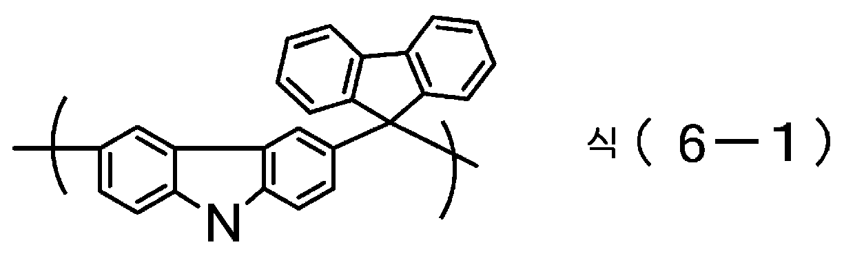
실시예 1Example 1
합성예 1에서 얻은 수지 2g에, 계면활성제로서 MEGAFAC R-30(Dainippon Ink And Chenicals, Inc.제, 상품명) 0.006g을 혼합하고, 시클로헥사논 8g에 용해시켜 용액으로 하였다. 그 후, 구멍직경 0.10μm의 폴리에틸렌제 마이크로필터를 이용하여 여과하고, 다시, 구멍직경 0.05μm의 폴리에틸렌제 마이크로필터를 이용하여 여과해서, 다층막에 의한 리소그래피 프로세스에 이용하는 레지스트 하층막 형성 조성물의 용액을 조제하였다.
To 2 g of the resin obtained in Synthesis Example 1, 0.006 g of MEGAFAC R-30 (manufactured by Dainippon Ink And Chenicals, Inc., trade name) as a surfactant was mixed and dissolved in 8 g of cyclohexanone to obtain a solution. Thereafter, the solution is filtered using a polyethylene microfilter having a pore diameter of 0.10 μm, and then filtered using a polyethylene microfilter having a pore diameter of 0.05 μm to obtain a solution of the resist underlayer film forming composition used in a lithography process using a multilayer film. prepared.
실시예 2Example 2
합성예 2에서 얻은 수지 2g에, 계면활성제로서 MEGAFAC R-30(Dainippon Ink And Chenicals, Inc.제, 상품명) 0.006g을 혼합하고, 시클로헥사논 8g에 용해시켜 용액으로 하였다. 그 후, 구멍직경 0.10μm의 폴리에틸렌제 마이크로필터를 이용하여 여과하고, 다시, 구멍직경 0.05μm의 폴리에틸렌제 마이크로필터를 이용하여 여과해서, 다층막에 의한 리소그래피 프로세스에 이용하는 레지스트 하층막 형성 조성물의 용액을 조제하였다.
To 2 g of the resin obtained in Synthesis Example 2, 0.006 g of MEGAFAC R-30 (manufactured by Dainippon Ink And Chenicals, Inc., trade name) as a surfactant was mixed and dissolved in 8 g of cyclohexanone to obtain a solution. Thereafter, the solution is filtered using a polyethylene microfilter having a pore diameter of 0.10 μm, and then filtered using a polyethylene microfilter having a pore diameter of 0.05 μm to obtain a solution of the resist underlayer film forming composition used in a lithography process using a multilayer film. prepared.
실시예 3Example 3
합성예 3에서 얻은 수지 2g에, 계면활성제로서 MEGAFAC R-30(Dainippon Ink And Chenicals, Inc.제, 상품명) 0.006g을 혼합하고, 프로필렌글리콜모노메틸에테르아세테이트 8g에 용해시켜 용액으로 하였다. 그 후, 구멍직경 0.10μm의 폴리에틸렌제 마이크로필터를 이용하여 여과하고, 다시, 구멍직경 0.05μm의 폴리에틸렌제 마이크로필터를 이용하여 여과해서, 다층막에 의한 리소그래피 프로세스에 이용하는 레지스트 하층막 형성 조성물의 용액을 조제하였다.
In 2 g of the resin obtained in Synthesis Example 3, 0.006 g of MEGAFAC R-30 (manufactured by Dainippon Ink And Chenicals, Inc., trade name) as a surfactant was mixed, and dissolved in 8 g of propylene glycol monomethyl ether acetate to obtain a solution. Thereafter, the solution is filtered using a polyethylene microfilter having a pore diameter of 0.10 μm, and then filtered using a polyethylene microfilter having a pore diameter of 0.05 μm to obtain a solution of the resist underlayer film forming composition used in a lithography process using a multilayer film. prepared.
실시예 4Example 4
합성예 4에서 얻은 수지 2g에, 계면활성제로서 MEGAFAC R-30(Dainippon Ink And Chenicals, Inc.제, 상품명) 0.006g을 혼합하고, 시클로헥사논 8g에 용해시켜 용액으로 하였다. 그 후, 구멍직경 0.10μm의 폴리에틸렌제 마이크로필터를 이용하여 여과하고, 다시, 구멍직경 0.05μm의 폴리에틸렌제 마이크로필터를 이용하여 여과해서, 다층막에 의한 리소그래피 프로세스에 이용하는 레지스트 하층막 형성 조성물의 용액을 조제하였다.
To 2 g of the resin obtained in Synthesis Example 4, 0.006 g of MEGAFAC R-30 (manufactured by Dainippon Ink And Chenicals, Inc., trade name) as a surfactant was mixed and dissolved in 8 g of cyclohexanone to obtain a solution. Thereafter, it is filtered using a polyethylene microfilter having a pore diameter of 0.10 μm, and again filtered using a polyethylene microfilter having a pore diameter of 0.05 μm to obtain a solution of the resist underlayer film forming composition used in a lithography process using a multilayer film. prepared.
비교예 1Comparative Example 1
시판의 크레졸노볼락수지(크레졸과 포름알데히드를 이용하여 얻어진 노볼락수지) 2g에, 계면활성제로서 MEGAFAC R-30(Dainippon Ink And Chenicals, Inc.제, 상품명) 0.006g을 혼합하고, 프로필렌글리콜모노메틸에테르아세테이트 8g에 용해시켜 용액으로 하였다. 그 후, 구멍직경 0.10μm의 폴리에틸렌제 마이크로필터를 이용하여 여과하고, 다시, 구멍직경 0.05μm의 폴리에틸렌제 마이크로필터를 이용하여 여과해서, 다층막에 의한 리소그래피 프로세스에 이용하는 레지스트 하층막 형성 조성물의 용액을 조제하였다.
0.006 g of MEGAFAC R-30 (manufactured by Dainippon Ink And Chenicals, Inc., trade name) as a surfactant is mixed with 2 g of a commercially available cresol novolak resin (a novolak resin obtained by using cresol and formaldehyde), and propylene glycol mono It was dissolved in 8 g of methyl ether acetate to obtain a solution. Thereafter, the solution is filtered using a polyethylene microfilter having a pore diameter of 0.10 μm, and then filtered using a polyethylene microfilter having a pore diameter of 0.05 μm to obtain a solution of the resist underlayer film forming composition used in a lithography process using a multilayer film. prepared.
비교예 2Comparative Example 2
비교합성예 1에서 얻은 수지 2g에, 계면활성제로서 MEGAFAC R-30(Dainippon Ink And Chenicals, Inc.제, 상품명) 0.006g을 혼합하고, 프로필렌글리콜모노메틸에테르아세테이트 8g에 용해시켜 용액으로 하였다. 그 후, 구멍직경 0.10μm의 폴리에틸렌제 마이크로필터를 이용하여 여과하고, 다시, 구멍직경 0.05μm의 폴리에틸렌제 마이크로필터를 이용하여 여과해서, 다층막에 의한 리소그래피 프로세스에 이용하는 레지스트 하층막 형성 조성물의 용액을 조제하였다.
To 2 g of the resin obtained in Comparative Synthesis Example 1, 0.006 g of MEGAFAC R-30 (manufactured by Dainippon Ink And Chenicals, Inc., trade name) as a surfactant was mixed and dissolved in 8 g of propylene glycol monomethyl ether acetate to obtain a solution. Thereafter, the solution is filtered using a polyethylene microfilter having a pore diameter of 0.10 μm, and then filtered using a polyethylene microfilter having a pore diameter of 0.05 μm to obtain a solution of the resist underlayer film forming composition used in a lithography process using a multilayer film. prepared.
(포토레지스트용제에 대한 용출시험)(Dissolution test for photoresist solvent)
실시예 1 내지 4 및 비교예 1에서 조제한 레지스트 하층막 형성 조성물의 용액을, 각각 스핀코터를 이용하여 실리콘웨이퍼 상에 도포하였다. 핫플레이트 상에서 400℃ 2분간 소성하고, 레지스트 하층막(막두께 0.30μm)을 형성하였다. 이 레지스트 하층막을 레지스트에 사용하는 용제, 예를 들어 유산에틸, 그리고 프로필렌글리콜모노메틸에테르, 프로필렌글리콜모노메틸에테르아세테이트, 시클로헥사논에 침지하고, 이들 용제에 불용인 것을 확인하였다.
The solutions of the resist underlayer film forming compositions prepared in Examples 1 to 4 and Comparative Example 1 were respectively applied onto a silicon wafer using a spin coater. It baked for 2 minutes at 400 degreeC on the hotplate, and the resist underlayer film (film thickness 0.30 micrometer) was formed. This resist underlayer film was immersed in the solvent used for a resist, for example, ethyl lactate, propylene glycol monomethyl ether, propylene glycol monomethyl ether acetate, and cyclohexanone, and it was confirmed that it is insoluble in these solvents.
(드라이에칭속도의 측정)(Measurement of dry etching rate)
드라이에칭속도의 측정에 이용한 에처 및 에칭가스는 이하의 것을 이용하였다.As the etcher and etching gas used for the measurement of the dry etching rate, the following were used.
ES401(Nippon Scientific Co., Ltd.제): CF4 ES401 (manufactured by Nippon Scientific Co., Ltd.): CF 4
실시예 1 내지 4 및 비교예 1에서 조제한 레지스트 하층막 형성 조성물의 용액을, 각각 스핀코터를 이용하여 실리콘웨이퍼 상에 도포하였다. 핫플레이트 상에서 240℃ 1분간, 또는 400℃ 2분간 소성하고, 레지스트 하층막(막두께 0.30μm)을 형성하였다. 에칭가스로서 CF4가스를 사용하여 드라이에칭속도를 측정하였다.The solutions of the resist underlayer film forming compositions prepared in Examples 1 to 4 and Comparative Example 1 were respectively applied onto a silicon wafer using a spin coater. It baked on a hotplate for 1 minute at 240 degreeC, or 400 degreeC for 2 minutes, and the resist underlayer film (film thickness 0.30 micrometer) was formed. Dry etching rate was measured using CF 4 gas as an etching gas.
또한, 마찬가지로 페놀노볼락수지(시판품, GPC에 의한 폴리스티렌 환산으로 측정되는 중량평균 분자량Mw은 2000, 다분산도Mw/Mn는 2.5)용액을, 스핀코터를 이용하여 실리콘웨이퍼 상에 도포하고, 205℃ 1분간 소성하여 도막을 형성하였다. 에칭가스로서 CF4가스를 사용하여 드라이에칭속도를 측정하였다. 205℃ 1분간 소성하여 얻어진 페놀노볼락수지막(막두께 0.2μm)의 에칭속도를 1.00으로 했을 때의 실시예 1 내지 4 및 비교예 1의 레지스트 하층막의 드라이에칭속도의 비교를 행하였다. 결과를 표 1에 나타냈다. 속도비는 (레지스트 하층막)/(페놀노볼락수지막)의 드라이에칭속도비이다.Similarly, a solution of a phenol novolak resin (commercial product, weight average molecular weight Mw measured in terms of polystyrene by GPC is 2000, polydispersity Mw/Mn is 2.5) is applied on a silicon wafer using a spin coater, 205 The coating film was formed by baking at ℃ for 1 minute. Dry etching rate was measured using CF 4 gas as an etching gas. The dry etching rates of the resist underlayer films of Examples 1 to 4 and Comparative Example 1 were compared when the etching rate of the phenol novolak resin film (film thickness 0.2 µm) obtained by baking at 205°C for 1 minute was set to 1.00. The results are shown in Table 1. The rate ratio is a dry etching rate ratio of (resist underlayer film)/(phenol novolak resin film).
[표 1][Table 1]
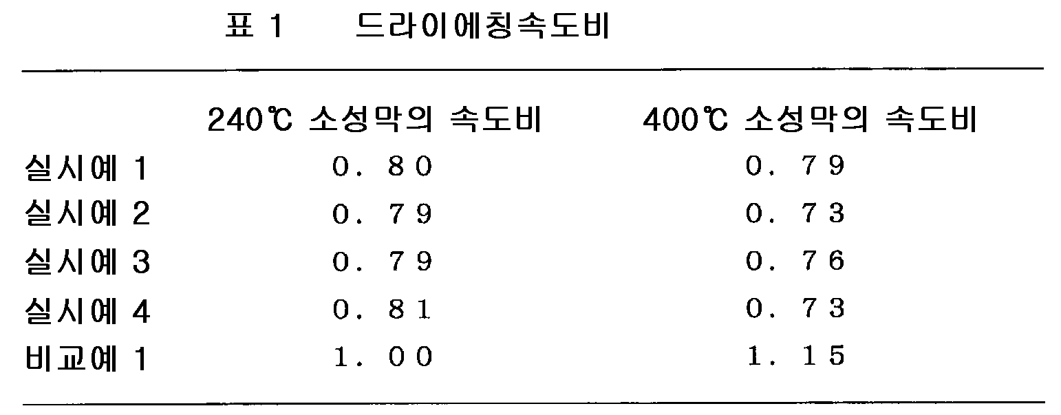
(홀웨이퍼에 대한 매립성 시험)(Filling test on whole wafer)
실시예 1 내지 4 및 비교예 2에서 조제한 레지스트 하층막 형성 조성물의 용액을, 각각 스핀코터를 이용하여 홀웨이퍼 상에 도포하였다. 핫플레이트 상에서 400℃ 2분간 소성하고, 레지스트 하층막(막두께 0.25μm)을 형성하였다. 홀웨이퍼로서 직경 100nm, 높이 400nm의 홀패턴을 이용하였다.The solutions of the resist underlayer film forming compositions prepared in Examples 1 to 4 and Comparative Example 2 were respectively applied onto the hole wafer using a spin coater. It baked for 2 minutes at 400 degreeC on the hotplate, and the resist underlayer film (thickness 0.25 micrometer) was formed. A hole pattern having a diameter of 100 nm and a height of 400 nm was used as a hole wafer.
실시예 1 내지 4에서 조제된 레지스트 하층막 형성 조성물의 용액을, 스핀코터를 이용하여 홀웨이퍼 상에 도포하고, 400℃ 2분간의 소성을 행한 후의 기판을 절단해서, 전자현미경으로 관찰한 도 1 내지 4의 사진에서는, 홀 내부까지 충분히 충전되어 있는 것을 알 수 있다.The solution of the resist underlayer film forming composition prepared in Examples 1 to 4 was applied on a hole wafer using a spin coater, and the substrate after baking at 400° C. for 2 minutes was cut and observed with an electron microscope. In the photographs of to 4, it can be seen that the interior of the hole is sufficiently filled.
한편, 비교예 2에서 조제된 레지스트 하층막 형성 조성물의 용액을, 스핀코터를 이용하여 홀웨이퍼 상에 도포하고, 400℃ 2분간의 소성을 행한 후의 기판을 절단해서, 전자현미경으로 관찰한 도 5의 사진에서는, 홀 내부에 약간이지만 부분적으로 공동이 존재하였다.
On the other hand, the solution of the resist underlayer film forming composition prepared in Comparative Example 2 was applied on the hole wafer using a spin coater, and the substrate after baking at 400° C. for 2 minutes was cut and observed with an electron microscope. In the photo of , there was a slight but partial void inside the hall.
[산업상의 이용가능성][Industrial Applicability]
본 발명의 다층막에 의한 리소그래피 프로세스에 이용하는 레지스트 하층막재료는, 종래의 고에칭레이트성 반사방지막과는 달리, 포토레지스트에 가깝거나 또는 포토레지스트에 비해 작은 드라이에칭속도의 선택비, 반도체기판에 비해 작은 드라이에칭속도의 선택비를 갖고, 나아가 반사방지막으로서의 효과도 겸비할 수 있는 레지스트 하층막을 제공할 수 있다. 또한, 본 발명의 하층막 재료는 상층에 증착으로 하드마스크를 형성가능한 내열성을 갖는다.
The resist underlayer film material used in the lithography process using the multilayer film of the present invention, unlike the conventional high etching rate antireflection film, has a dry etching rate selectivity close to or smaller than that of photoresist, compared to semiconductor substrates. It is possible to provide a resist underlayer film having a small dry etching rate selectivity and further having an effect as an antireflection film. Further, the underlayer film material of the present invention has heat resistance capable of forming a hard mask by vapor deposition on the upper layer.
Claims (9)
상기 노볼락폴리머가 식(1):

(식(1) 중, R1은 수소원자의 치환기로서, 할로겐기, 니트로기, 아미노기, 하이드록시기, 탄소수 1 내지 10의 알킬기, 탄소수 2 내지 10의 알케닐기, 탄소수 6 내지 40의 아릴기, 또는 에테르결합, 케톤결합, 혹은 에스테르결합을 포함할 수도 있는 이들의 조합이며, R2는 메틸기 또는 벤질기이며, R3은 수소원자, 또는 할로겐기, 니트로기, 아미노기, 포밀기, 카르복실기, 카르본산알킬에스테르기, 하이드록시기로 치환될 수도 있는 탄소수 6 내지 40의 아릴기, 또는 복소환기이며, R4는 수소원자, 또는 할로겐기, 니트로기, 아미노기, 포밀기, 카르복실기, 카르본산알킬에스테르기, 하이드록시기로 치환될 수도 있는 탄소수 1 내지 10의 알킬기, 탄소수 6 내지 40의 아릴기, 또는 복소환기이며, R3과 R4는 이들이 결합하는 탄소원자와 함께 환을 형성할 수도 있다. n은 0이며, m은 0이다.)로 표시되는 단위구조를 포함하는 것인, 리소그래피 공정에 이용하는 레지스트 하층막 형성 조성물.A novolac polymer obtained by reaction of an aromatic compound having a second amino group and an aldehyde compound,
The novolac polymer has formula (1):
(In formula (1), R 1 is a substituent of a hydrogen atom, and is a halogen group, a nitro group, an amino group, a hydroxy group, an alkyl group having 1 to 10 carbon atoms, an alkenyl group having 2 to 10 carbon atoms, or an aryl group having 6 to 40 carbon atoms. , or a combination thereof which may contain an ether bond, a ketone bond, or an ester bond, R 2 is a methyl group or a benzyl group, R 3 is a hydrogen atom, or a halogen group, nitro group, amino group, formyl group, carboxyl group, A carboxylic acid alkyl ester group, an aryl group having 6 to 40 carbon atoms optionally substituted with a hydroxy group, or a heterocyclic group, R 4 is a hydrogen atom, or a halogen group, a nitro group, an amino group, a formyl group, a carboxyl group, a carboxylate alkyl ester a group, an alkyl group having 1 to 10 carbon atoms, an aryl group having 6 to 40 carbon atoms, or a heterocyclic group optionally substituted with a hydroxy group, and R 3 and R 4 may form a ring together with the carbon atom to which they are bonded. is 0, and m is 0.) A composition for forming a resist underlayer film for use in a lithography process, comprising a unit structure represented by
R3이 페닐기, 나프틸기, 안트릴기, 또는 피레닐기이며, R4가 수소원자인 레지스트 하층막 형성 조성물.According to claim 1,
A composition for forming a resist underlayer film , wherein R 3 is a phenyl group, a naphthyl group, an anthryl group, or a pyrenyl group, and R 4 is a hydrogen atom.
추가로 가교제를 함유하는 레지스트 하층막 형성 조성물.According to claim 1,
A resist underlayer film forming composition further comprising a crosslinking agent.
추가로 산 및 산발생제 중 적어도 하나를 포함하는 레지스트 하층막 형성 조성물.According to claim 1,
A resist underlayer film forming composition further comprising at least one of an acid and an acid generator.
Applications Claiming Priority (3)
| Application Number | Priority Date | Filing Date | Title |
|---|---|---|---|
| JPJP-P-2013-269765 | 2013-12-26 | ||
| JP2013269765 | 2013-12-26 | ||
| PCT/JP2014/083130 WO2015098594A1 (en) | 2013-12-26 | 2014-12-15 | Resist underlayer film-forming composition containing novolac polymer having secondary amino group |
Publications (2)
| Publication Number | Publication Date |
|---|---|
| KR20160102985A KR20160102985A (en) | 2016-08-31 |
| KR102327785B1 true KR102327785B1 (en) | 2021-11-17 |
Family
ID=53478458
Family Applications (1)
| Application Number | Title | Priority Date | Filing Date |
|---|---|---|---|
| KR1020167015213A Active KR102327785B1 (en) | 2013-12-26 | 2014-12-15 | Resist underlayer film-forming composition containing novolac polymer having secondary amino group |
Country Status (6)
| Country | Link |
|---|---|
| US (1) | US11199777B2 (en) |
| JP (1) | JP6583630B2 (en) |
| KR (1) | KR102327785B1 (en) |
| CN (1) | CN105874386B (en) |
| TW (1) | TWI713445B (en) |
| WO (1) | WO2015098594A1 (en) |
Families Citing this family (20)
| Publication number | Priority date | Publication date | Assignee | Title |
|---|---|---|---|---|
| JP7176844B2 (en) * | 2015-10-19 | 2022-11-22 | 日産化学株式会社 | Composition for forming resist underlayer film containing long-chain alkyl group-containing novolak |
| KR101852457B1 (en) | 2015-11-12 | 2018-04-26 | 삼성에스디아이 주식회사 | The resin composition included novel polymer and organic film using the same |
| WO2018043410A1 (en) * | 2016-09-01 | 2018-03-08 | 日産化学工業株式会社 | Resist underlayer film forming composition containing triaryldiamine-containing novolac resin |
| WO2018131562A1 (en) * | 2017-01-13 | 2018-07-19 | 日産化学工業株式会社 | Amide solvent-containing resist underlayer film-forming composition |
| CN108628102B (en) * | 2017-03-21 | 2021-07-27 | 东友精细化工有限公司 | Composition for hard mask |
| TWI770204B (en) * | 2017-06-23 | 2022-07-11 | 日商日產化學工業股份有限公司 | Resist underlayer film forming composition having improved flattening property |
| JP7092132B2 (en) * | 2017-07-27 | 2022-06-28 | 日産化学株式会社 | A composition for forming a release layer and a release layer |
| JP6726142B2 (en) | 2017-08-28 | 2020-07-22 | 信越化学工業株式会社 | Organic film forming composition, semiconductor device manufacturing substrate, organic film forming method, pattern forming method, and polymer |
| JP6940335B2 (en) | 2017-08-30 | 2021-09-29 | 信越化学工業株式会社 | Organic film forming composition, semiconductor device manufacturing substrate, organic film forming method, pattern forming method, and polymer |
| JP7331699B2 (en) * | 2017-12-22 | 2023-08-23 | 日産化学株式会社 | Protective film-forming composition having acetal structure |
| KR102358171B1 (en) * | 2018-01-30 | 2022-02-03 | 동우 화인켐 주식회사 | Composition for hard mask |
| KR20210036863A (en) * | 2018-08-01 | 2021-04-05 | 니폰 가야꾸 가부시끼가이샤 | Aromatic amine resin having an N-alkyl group, curable resin composition, and cured product thereof |
| JP7161451B2 (en) | 2019-07-05 | 2022-10-26 | 信越化学工業株式会社 | Composition for forming organic film, substrate for manufacturing semiconductor device, method for forming organic film, and method for forming pattern |
| WO2021039843A1 (en) * | 2019-08-27 | 2021-03-04 | 三菱瓦斯化学株式会社 | Composition for forming film for lithography, resist pattern forming method, circuit pattern forming method and purification method |
| US11567408B2 (en) * | 2019-10-15 | 2023-01-31 | Rohm And Haas Electronic Materials Korea Ltd. | Coating composition for use with an overcoated photoresist |
| JP7349887B2 (en) * | 2019-10-31 | 2023-09-25 | 東京応化工業株式会社 | Composition for forming hard mask and method for producing electronic components |
| CN115427891A (en) * | 2020-03-30 | 2022-12-02 | 日产化学株式会社 | Composition for forming resist underlayer film |
| JP7768131B2 (en) * | 2020-08-05 | 2025-11-12 | 日産化学株式会社 | Resist underlayer film-forming composition |
| JP2023101149A (en) * | 2022-01-07 | 2023-07-20 | 東京応化工業株式会社 | Composition for forming resist underlayer film, method for forming resist pattern, method for forming pattern of resist underlayer film, and method for forming pattern |
| CN116554444B (en) * | 2023-06-15 | 2024-03-29 | 嘉庚创新实验室 | Polymers for use in photolithographic media compositions and photolithographic media compositions |
Citations (4)
| Publication number | Priority date | Publication date | Assignee | Title |
|---|---|---|---|---|
| JP2004205676A (en) | 2002-12-24 | 2004-07-22 | Shin Etsu Chem Co Ltd | Pattern forming method and underlayer film forming material |
| US20050003202A1 (en) * | 2002-09-05 | 2005-01-06 | Gerber Arthur H. | N-substituted arylamino-phenol-formaldehyde condensates |
| JP2005114921A (en) | 2003-10-06 | 2005-04-28 | Shin Etsu Chem Co Ltd | Resist underlayer film material and pattern forming method |
| WO2013047516A1 (en) * | 2011-09-29 | 2013-04-04 | 日産化学工業株式会社 | Diarylamine novolac resin |
Family Cites Families (16)
| Publication number | Priority date | Publication date | Assignee | Title |
|---|---|---|---|---|
| JP2793251B2 (en) | 1989-05-09 | 1998-09-03 | 株式会社東芝 | Pattern formation method |
| JPH04268559A (en) | 1991-02-22 | 1992-09-24 | Konica Corp | Damping waterless |
| JP4213876B2 (en) * | 2001-04-13 | 2009-01-21 | 富士フイルム株式会社 | Photosensitive composition and negative planographic printing plate |
| JP2004198632A (en) | 2002-12-17 | 2004-07-15 | Nippon Zeon Co Ltd | Radiation-sensitive resin composition |
| JP2004198812A (en) | 2002-12-19 | 2004-07-15 | Nippon Zeon Co Ltd | Radiation-sensitive resin composition |
| JP4895049B2 (en) | 2005-06-10 | 2012-03-14 | 日産化学工業株式会社 | Lithographic coating-type underlayer film forming composition containing naphthalene resin derivative |
| KR100665758B1 (en) | 2005-09-15 | 2007-01-09 | 제일모직주식회사 | Hard mask composition having antireflection |
| JP4421566B2 (en) | 2005-12-26 | 2010-02-24 | チェイル インダストリーズ インコーポレイテッド | Hard mask composition for photoresist underlayer film and method of manufacturing semiconductor integrated circuit device using the same |
| JP4659678B2 (en) | 2005-12-27 | 2011-03-30 | 信越化学工業株式会社 | Photoresist underlayer film forming material and pattern forming method |
| JP5641253B2 (en) | 2009-06-19 | 2014-12-17 | 日産化学工業株式会社 | Carbazole novolac resin |
| JP5867732B2 (en) | 2010-12-09 | 2016-02-24 | 日産化学工業株式会社 | Resist underlayer film forming composition containing hydroxyl group-containing carbazole novolak resin |
| WO2013115097A1 (en) | 2012-02-01 | 2013-08-08 | 日産化学工業株式会社 | Resist underlayer film forming composition containing copolymer resin having heterocyclic ring |
| WO2013146670A1 (en) * | 2012-03-27 | 2013-10-03 | 日産化学工業株式会社 | Resist underlayer film-forming composition which contains phenylindole-containing novolac resin |
| JP6119669B2 (en) | 2013-06-11 | 2017-04-26 | 信越化学工業株式会社 | Underlayer film material and pattern forming method |
| JP6476857B2 (en) * | 2014-12-29 | 2019-03-06 | 日亜化学工業株式会社 | Light emitting device |
| CN107378217A (en) | 2017-08-24 | 2017-11-24 | 安徽苏立科技股份有限公司 | A kind of full-automatic nut-welding system for special-shaped heating tube production line balance |
-
2014
- 2014-12-15 KR KR1020167015213A patent/KR102327785B1/en active Active
- 2014-12-15 WO PCT/JP2014/083130 patent/WO2015098594A1/en not_active Ceased
- 2014-12-15 JP JP2015554753A patent/JP6583630B2/en active Active
- 2014-12-15 CN CN201480070504.9A patent/CN105874386B/en active Active
- 2014-12-15 US US15/108,350 patent/US11199777B2/en active Active
- 2014-12-19 TW TW103144520A patent/TWI713445B/en active
Patent Citations (4)
| Publication number | Priority date | Publication date | Assignee | Title |
|---|---|---|---|---|
| US20050003202A1 (en) * | 2002-09-05 | 2005-01-06 | Gerber Arthur H. | N-substituted arylamino-phenol-formaldehyde condensates |
| JP2004205676A (en) | 2002-12-24 | 2004-07-22 | Shin Etsu Chem Co Ltd | Pattern forming method and underlayer film forming material |
| JP2005114921A (en) | 2003-10-06 | 2005-04-28 | Shin Etsu Chem Co Ltd | Resist underlayer film material and pattern forming method |
| WO2013047516A1 (en) * | 2011-09-29 | 2013-04-04 | 日産化学工業株式会社 | Diarylamine novolac resin |
Also Published As
| Publication number | Publication date |
|---|---|
| JPWO2015098594A1 (en) | 2017-03-23 |
| KR20160102985A (en) | 2016-08-31 |
| US11199777B2 (en) | 2021-12-14 |
| CN105874386A (en) | 2016-08-17 |
| JP6583630B2 (en) | 2019-10-02 |
| TWI713445B (en) | 2020-12-21 |
| WO2015098594A1 (en) | 2015-07-02 |
| TW201538609A (en) | 2015-10-16 |
| US20160326396A1 (en) | 2016-11-10 |
| CN105874386B (en) | 2019-12-06 |
Similar Documents
| Publication | Publication Date | Title |
|---|---|---|
| KR102327785B1 (en) | Resist underlayer film-forming composition containing novolac polymer having secondary amino group | |
| KR102072490B1 (en) | Resist underlayer film-forming composition which contains phenylindole-containing novolac resin | |
| JP5641253B2 (en) | Carbazole novolac resin | |
| JP6004172B2 (en) | Lithographic resist underlayer film forming composition containing carbonyl group-containing carbazole novolak | |
| JP6137486B2 (en) | Resist underlayer film forming composition containing copolymer resin containing heterocycle | |
| JP6734569B2 (en) | Resist underlayer film forming composition containing pinol novolac resin | |
| JP6066092B2 (en) | Diarylamine novolac resin | |
| US9263285B2 (en) | Composition for forming a resist underlayer film including hydroxyl group-containing carbazole novolac resin | |
| KR102155115B1 (en) | Resist underlayer film-forming composition comprising carbonyl-containing polyhydroxy aromatic ring novolac resin | |
| KR102432622B1 (en) | A composition for forming a resist underlayer film comprising a triaryldiamine-containing novolak resin | |
| JP6338048B2 (en) | Iminostilbene polymer and resist underlayer film forming composition containing the same |
Legal Events
| Date | Code | Title | Description |
|---|---|---|---|
| PA0105 | International application |
St.27 status event code: A-0-1-A10-A15-nap-PA0105 |
|
| PG1501 | Laying open of application |
St.27 status event code: A-1-1-Q10-Q12-nap-PG1501 |
|
| R18-X000 | Changes to party contact information recorded |
St.27 status event code: A-3-3-R10-R18-oth-X000 |
|
| P11-X000 | Amendment of application requested |
St.27 status event code: A-2-2-P10-P11-nap-X000 |
|
| P13-X000 | Application amended |
St.27 status event code: A-2-2-P10-P13-nap-X000 |
|
| PA0201 | Request for examination |
St.27 status event code: A-1-2-D10-D11-exm-PA0201 |
|
| D13-X000 | Search requested |
St.27 status event code: A-1-2-D10-D13-srh-X000 |
|
| D14-X000 | Search report completed |
St.27 status event code: A-1-2-D10-D14-srh-X000 |
|
| E902 | Notification of reason for refusal | ||
| PE0902 | Notice of grounds for rejection |
St.27 status event code: A-1-2-D10-D21-exm-PE0902 |
|
| T11-X000 | Administrative time limit extension requested |
St.27 status event code: U-3-3-T10-T11-oth-X000 |
|
| T11-X000 | Administrative time limit extension requested |
St.27 status event code: U-3-3-T10-T11-oth-X000 |
|
| T11-X000 | Administrative time limit extension requested |
St.27 status event code: U-3-3-T10-T11-oth-X000 |
|
| T11-X000 | Administrative time limit extension requested |
St.27 status event code: U-3-3-T10-T11-oth-X000 |
|
| E13-X000 | Pre-grant limitation requested |
St.27 status event code: A-2-3-E10-E13-lim-X000 |
|
| P11-X000 | Amendment of application requested |
St.27 status event code: A-2-2-P10-P11-nap-X000 |
|
| P13-X000 | Application amended |
St.27 status event code: A-2-2-P10-P13-nap-X000 |
|
| E701 | Decision to grant or registration of patent right | ||
| PE0701 | Decision of registration |
St.27 status event code: A-1-2-D10-D22-exm-PE0701 |
|
| PR0701 | Registration of establishment |
St.27 status event code: A-2-4-F10-F11-exm-PR0701 |
|
| PR1002 | Payment of registration fee |
St.27 status event code: A-2-2-U10-U12-oth-PR1002 Fee payment year number: 1 |
|
| PG1601 | Publication of registration |
St.27 status event code: A-4-4-Q10-Q13-nap-PG1601 |
|
| PR1001 | Payment of annual fee |
St.27 status event code: A-4-4-U10-U11-oth-PR1001 Fee payment year number: 4 |
|
| P22-X000 | Classification modified |
St.27 status event code: A-4-4-P10-P22-nap-X000 |