KR102326518B1 - Wear Leveling for Random Access and Ferroelectric Memory - Google Patents
Wear Leveling for Random Access and Ferroelectric Memory Download PDFInfo
- Publication number
- KR102326518B1 KR102326518B1 KR1020207008659A KR20207008659A KR102326518B1 KR 102326518 B1 KR102326518 B1 KR 102326518B1 KR 1020207008659 A KR1020207008659 A KR 1020207008659A KR 20207008659 A KR20207008659 A KR 20207008659A KR 102326518 B1 KR102326518 B1 KR 102326518B1
- Authority
- KR
- South Korea
- Prior art keywords
- data
- section
- latches
- memory cells
- row
- Prior art date
- Legal status (The legal status is an assumption and is not a legal conclusion. Google has not performed a legal analysis and makes no representation as to the accuracy of the status listed.)
- Active
Links
Images


Classifications
-
- G—PHYSICS
- G11—INFORMATION STORAGE
- G11C—STATIC STORES
- G11C11/00—Digital stores characterised by the use of particular electric or magnetic storage elements; Storage elements therefor
- G11C11/21—Digital stores characterised by the use of particular electric or magnetic storage elements; Storage elements therefor using electric elements
- G11C11/22—Digital stores characterised by the use of particular electric or magnetic storage elements; Storage elements therefor using electric elements using ferroelectric elements
- G11C11/225—Auxiliary circuits
- G11C11/2273—Reading or sensing circuits or methods
-
- G—PHYSICS
- G11—INFORMATION STORAGE
- G11C—STATIC STORES
- G11C11/00—Digital stores characterised by the use of particular electric or magnetic storage elements; Storage elements therefor
- G11C11/21—Digital stores characterised by the use of particular electric or magnetic storage elements; Storage elements therefor using electric elements
- G11C11/22—Digital stores characterised by the use of particular electric or magnetic storage elements; Storage elements therefor using electric elements using ferroelectric elements
- G11C11/225—Auxiliary circuits
- G11C11/2253—Address circuits or decoders
-
- G—PHYSICS
- G06—COMPUTING OR CALCULATING; COUNTING
- G06F—ELECTRIC DIGITAL DATA PROCESSING
- G06F11/00—Error detection; Error correction; Monitoring
- G06F11/07—Responding to the occurrence of a fault, e.g. fault tolerance
- G06F11/08—Error detection or correction by redundancy in data representation, e.g. by using checking codes
- G06F11/10—Adding special bits or symbols to the coded information, e.g. parity check, casting out 9's or 11's
- G06F11/1008—Adding special bits or symbols to the coded information, e.g. parity check, casting out 9's or 11's in individual solid state devices
- G06F11/1048—Adding special bits or symbols to the coded information, e.g. parity check, casting out 9's or 11's in individual solid state devices using arrangements adapted for a specific error detection or correction feature
-
- G—PHYSICS
- G11—INFORMATION STORAGE
- G11C—STATIC STORES
- G11C11/00—Digital stores characterised by the use of particular electric or magnetic storage elements; Storage elements therefor
- G11C11/21—Digital stores characterised by the use of particular electric or magnetic storage elements; Storage elements therefor using electric elements
- G11C11/22—Digital stores characterised by the use of particular electric or magnetic storage elements; Storage elements therefor using electric elements using ferroelectric elements
- G11C11/221—Digital stores characterised by the use of particular electric or magnetic storage elements; Storage elements therefor using electric elements using ferroelectric elements using ferroelectric capacitors
-
- G—PHYSICS
- G11—INFORMATION STORAGE
- G11C—STATIC STORES
- G11C11/00—Digital stores characterised by the use of particular electric or magnetic storage elements; Storage elements therefor
- G11C11/21—Digital stores characterised by the use of particular electric or magnetic storage elements; Storage elements therefor using electric elements
- G11C11/22—Digital stores characterised by the use of particular electric or magnetic storage elements; Storage elements therefor using electric elements using ferroelectric elements
- G11C11/225—Auxiliary circuits
- G11C11/2275—Writing or programming circuits or methods
-
- G—PHYSICS
- G11—INFORMATION STORAGE
- G11C—STATIC STORES
- G11C11/00—Digital stores characterised by the use of particular electric or magnetic storage elements; Storage elements therefor
- G11C11/21—Digital stores characterised by the use of particular electric or magnetic storage elements; Storage elements therefor using electric elements
- G11C11/22—Digital stores characterised by the use of particular electric or magnetic storage elements; Storage elements therefor using electric elements using ferroelectric elements
- G11C11/225—Auxiliary circuits
- G11C11/2277—Verifying circuits or methods
-
- G—PHYSICS
- G11—INFORMATION STORAGE
- G11C—STATIC STORES
- G11C29/00—Checking stores for correct operation ; Subsequent repair; Testing stores during standby or offline operation
- G11C29/52—Protection of memory contents; Detection of errors in memory contents
Landscapes
- Engineering & Computer Science (AREA)
- Computer Hardware Design (AREA)
- Theoretical Computer Science (AREA)
- Quality & Reliability (AREA)
- Physics & Mathematics (AREA)
- General Engineering & Computer Science (AREA)
- General Physics & Mathematics (AREA)
- Power Engineering (AREA)
- For Increasing The Reliability Of Semiconductor Memories (AREA)
- Dram (AREA)
- Detection And Correction Of Errors (AREA)
- Memory System (AREA)
Abstract
랜덤 액세스 및 강유전체 메모리를 위한 웨어 레벨링과 관련된 방법들, 시스템들 및 디바이스들이 설명된다. 비휘발성 메모리 디바이스들, 예를 들어, 강유전체 랜덤 액세스 메모리(FeRAM)는 제한된 사이클링으로 인한 안전성 이슈들을 회피함으로써 메모리 디바이스들의 수명을 연장시키기 위해 웨어 레벨링을 이용할 수 있다. 웨어 레벨링 풀 또는웨어 레벨링 적용에 사용되는 셀들 수는 메모리 어레이의 동일한 섹션 내 소스 페이지와 대상 페이지에 대한 제한을 완화하거나 회피함으로써 확장될 수 있다. 또한, 소스 페이지로부터 대상 페이지로 데이터를 이동시킬 때 소스 페이지에 존재하는 중복 오류를 회피하기 위해 오류 정정 코드가 적용될 수있다.Methods, systems and devices related to wear leveling for random access and ferroelectric memory are described. Non-volatile memory devices, such as ferroelectric random access memory (FeRAM), may use wear leveling to extend the life of memory devices by avoiding safety issues due to limited cycling. The wear leveling pool or number of cells used for wear leveling application can be expanded by relaxing or avoiding restrictions on source and destination pages within the same section of the memory array. In addition, error correction codes may be applied to avoid duplicate errors present in the source page when moving data from the source page to the target page.
Description
상호 참조cross reference
본 특허 출원은 2017년 8월 30일자로 출원된 "Wear Leveling for Random Access and Ferroelectric Memory(랜덤 액세스 및 강유전체 메모리를 위한 웨어 레벨링)"라는 명칭의 Fackenthal 외의 미국 특허 출원 15/691,454호의 우선권을 주장하는, 2018년 8월 23일자로 출원된 "Wear Leveling for Random Access and Ferroelectric Memory"라는 명칭의 Fackenthal 외의 PCT 출원 PCT/US2018/047790호의 우선권을 주장하며, 이의 각각은 본 출원의 양수인에게 양도되고 이의 각각은 그 전문이 참고로 본 출원에 명확히 포함된다.This patent application claims priority to U.S. Patent Application Serial No. 15/691,454 to Fackenthal et al., entitled "Wear Leveling for Random Access and Ferroelectric Memory," filed on August 30, 2017. , claim priority to Fackenthal et al. PCT Application No. PCT/US2018/047790, filed Aug. 23, 2018, entitled "Wear Leveling for Random Access and Ferroelectric Memory," each of which is assigned to the assignee of this application and its respective is expressly incorporated herein by reference in its entirety.
다음은 개괄적으로 메모리 어레이, 보다 구체적으로는 랜덤 액세스 및 강유전체 메모리를 위한 웨어 레벨링에 관한 것이다.The following relates generally to memory arrays, and more specifically to wear leveling for random access and ferroelectric memories.
메모리 디바이스들은 컴퓨터들, 무선 통신 디바이스들, 카메라들, 디지털 디스플레이들 등과 같은 다양한 전자 디바이스에 정보를 저장하기 위해 널리 사용된다. 정보는 메모리 셀의 상이한 상태들을 프로그래밍함으로써 저장된다. 예를 들어, 2진 메모리 셀들은 보통 논리 "1" 또는 논리 "0"으로 표기되는 두 개의 상태를 갖는다. 그 외 다른 시스템들에서는, 세 개 이상의 상태가 저장될 수 있다. 저장된 정보에 액세스하기 위해, 전자 기기의 구성요소는 메모리 셀에 저장된 상태를 판독 또는 감지할 수 있다. 정보를 저장하기 위해, 전자 기기의 구성요소는 메모리 셀에 상태를 기록 또는 프로그래밍할 수 있다.BACKGROUND Memory devices are widely used for storing information in a variety of electronic devices, such as computers, wireless communication devices, cameras, digital displays, and the like. Information is stored by programming different states of the memory cell. For example, binary memory cells have two states, usually denoted as a logic "1" or a logic "0". In other systems, more than two states may be stored. To access the stored information, a component of the electronic device can read or sense the state stored in the memory cell. To store information, a component of an electronic device may write or program a state to a memory cell.
자기 하드 디스크들, 랜덤 액세스 메모리(RAM), 판독 전용 메모리(ROM), 동적 RAM(DRAM), 동기식 동적 RAM(SDRAM), 강유전 RAM(FeRAM), 자기 RAM(MRAM), 저항 RAM(RRAM), 플래시 메모리, 상 변화 메모리(PCM), 3-차원(3D) 크로스-포인트 메모리(3D XPoint™ 메모리), 3D 부정-곱(NAND) 메모리 등을 비롯하여, 다양한 유형의 메모리 디바이스가 존재한다. 메모리 디바이스들은 휘발성 또는 비휘발성일 수 있다. 비휘발성 메모리 디바이스들, 예를 들어, FeRAM은 외부 전원이 없을 때에도 장시간 그것들의 저장된 로직 상태를 유지할 수 있다. 휘발성 메모리 디바이스들, 예를 들어, DRAM은 외부 전원에 의해 주기적으로 리프레시되지 않는 한 시간이 지남에 따라 그것들의 저장된 상태를 잃을 수 있다. FeRAM은 유사한 디바이스 아키텍처들을 휘발성 메모리로서 사용할 수 있으나 강유전 커패시터를 저장 디바이스로서 사용함으로 인해 비휘발성 속성들을 가질 수 있다. 그에 따라 FeRAM 디바이스들은 그 외 다른 비휘발성 및 휘발성 메모리 디바이스들에 비해 개선된 성능을 가질 수 있다.magnetic hard disks, random access memory (RAM), read only memory (ROM), dynamic RAM (DRAM), synchronous dynamic RAM (SDRAM), ferroelectric RAM (FeRAM), magnetic RAM (MRAM), resistive RAM (RRAM), Various types of memory devices exist, including flash memory, phase change memory (PCM), three-dimensional (3D) cross-point memory (3D XPoint™ memory), 3D negative-product (NAND) memory, and the like. Memory devices may be volatile or non-volatile. Non-volatile memory devices, such as FeRAM, can retain their stored logic state for extended periods of time even in the absence of an external power source. Volatile memory devices, for example DRAM, can lose their stored state over time unless periodically refreshed by an external power source. FeRAM may use similar device architectures as volatile memory but may have non-volatile properties due to the use of a ferroelectric capacitor as a storage device. Accordingly, FeRAM devices may have improved performance compared to other non-volatile and volatile memory devices.
메모리 소자들을 개선하는 것은 일반적으로 그 외 다른 지표들 중에서도, 메모리 셀 밀도를 증가시키는 것, 판독/기록 속도를 증가시키는 것, 신뢰성을 증가시키는 것, 데이터 보존을 증가시키는 것, 전력 소모를 감소시키는 것 또는 제조 비용을 감소시키는 것을 포함할 수 있다. 그러나, 경우에 따라, 제한된 프로그램 및 소거 사이클링 내구성으로 인해 메모리 셀의 안정성이 제한되면 고객들이 경험하는 메모리 디바이스들의 성능과 수명에 부정적인 영향을 줄 수 있다.Improving memory devices generally results in increasing memory cell density, increasing read/write speed, increasing reliability, increasing data retention, reducing power consumption, among other indicators. or to reduce manufacturing costs. However, in some cases, when the stability of a memory cell is limited due to limited program and erase cycling endurance, it can negatively affect the performance and lifespan of memory devices that customers experience.
본 개시는 이하의 도면들을 참조하고 포함한다:
도 1은 본 개시의 실시 예들에 따른 랜덤 액세스 및 강유전체 메모리를 위한 웨어 레벨링을 지원하는 메모리 셀들의 어레이를 갖는 메모리 디바이스의 도해의 일례를 도시한다.
도 2는 본 개시의 실시 예들에 따른 랜덤 액세스 및 강유전체 메모리를 위한 웨어 레벨링을 지원하는 강유전체 메모리 셀 및 회로 구성요소들의 일례를 도시한다.
도 3은 본 개시의 실시 예들에 따른 랜덤 액세스 및 강유전체 메모리를 위한 웨어 레벨링을 지원하는 강유전체 메모리 셀에 대한 히스테리시트 곡선들로 비-선형 전기적 속성들의 일례를 도시한다.
도 4는 본 개시의 실시 예들에 따른 랜덤 액세스 및 강유전체 메모리를 위한 웨어 레벨링을 지원하는 동작들의 도해들을 도시한다.
도 5a 및 도 5b는 본 개시의 실시 예들에 따른 랜덤 액세스 및 강유전체 메모리를 위한 웨어 레벨링을 지원하는 동작들의 도시한다.
도 6은 본 개시의 실시 예들에 따른 랜덤 액세스 및 강유전체 메모리를 위한 웨어 레벨링을 지원하는 메모리 디바이스의 블록도를 도시한다.
도 7은 본 개시의 실시 예들에 따른 랜덤 액세스 및 강유전체 메모리를 위한 웨어 레벨링 방법을 도시하는 흐름도를 도시한다.
도 8은 본 개시의 실시 예들에 따른 랜덤 액세스 및 강유전체 메모리를 위한 웨어 레벨링 방법을 도시하는 흐름도를 도시한다.The present disclosure refers to and includes the following drawings:
1 shows an example of a schematic diagram of a memory device having an array of memory cells supporting wear leveling for random access and ferroelectric memory in accordance with embodiments of the present disclosure.
2 illustrates an example of a ferroelectric memory cell and circuit components supporting wear leveling for random access and ferroelectric memory according to embodiments of the present disclosure.
3 illustrates an example of non-linear electrical properties with hysteresis curves for a ferroelectric memory cell supporting wear leveling for random access and ferroelectric memory according to embodiments of the present disclosure;
4 illustrates diagrams of operations supporting wear leveling for random access and ferroelectric memory according to embodiments of the present disclosure.
5A and 5B illustrate operations supporting wear leveling for random access and ferroelectric memory according to embodiments of the present disclosure.
6 is a block diagram of a memory device supporting wear leveling for random access and ferroelectric memory according to embodiments of the present disclosure.
7 is a flowchart illustrating a wear leveling method for random access and ferroelectric memory according to embodiments of the present disclosure.
8 is a flowchart illustrating a wear leveling method for a random access and a ferroelectric memory according to embodiments of the present disclosure.
웨어 레벨링은 제한된 사이클링 성능을 보일 수 있는 비휘발성 메모리 디바이스들, 예를 들어, FeRAM의 사용 가능한 수명을 연장시킬 수 있다. 웨어 레벨링은 논리적 어드레스에 대응하는 메모리 셀들의 특정 부분 집합이 나머지 메모리 셀들과 비교할 때 증가된 수의 프로그램 및 소거 사이클을 거치게 하는 것을 회피하기 위해 상이한 메모리 셀 집합(즉,웨어 레벨링 풀)에 걸쳐 다수의 프로그램 및 소거 사이클을 분배할 수 있다.Wear leveling may extend the usable life of non-volatile memory devices that may exhibit limited cycling performance, eg, FeRAM. Wear leveling is performed by multiple across different sets of memory cells (i.e., wear leveling pools) to avoid having a particular subset of memory cells corresponding to a logical address undergo an increased number of program and erase cycles when compared to the rest of the memory cells. of program and erase cycles can be distributed.
웨어 레벨링 적용시,웨어 레벨링 풀이 클수록 웨어 레벨링이 더 효율적일 수 있다. 웨어 레벨링 풀은 데이터가 순환하는 어레이의 다수의 페이지를 지칭할 수 있다. 페이지는 다양한 인터페이스에서 하나의 유닛으로 취급되는 다수의 데이터를 지칭할 수 있고 메모리 어레이의 섹션에 공통인 워드 라인과 연관된 데이터 그룹과 관련될 수 있다. 예를 들어, FeRAM에서 페이지의 통상적인 크기는 64 바이트일 수 있다. 예를 들어, 128, 256, 512 바이트 등의 다른 크기의 페이지도 가능할 수 있다. 예로서, 웨어 레벨링 풀이 1,000 페이지이고, 고객이 하나의 논리적 페이지를 연속적으로 적중하는 경우, 그러한 고객 사이클들은 웨어 레벨링 풀 내 1,000 페이지에 걸쳐 분산될 수 있고 그에 따라 각 페이지가 거치는 물리적 사이클 수는 1,000배 감소될 수 있다. 반면에, 웨어 레벨링 풀이 32,000 페이지라면, 각 페이지가 거치는 물리적 사이클 수는 32,000배 감소될 수 있다. 그로 인해, 비휘발성 메모리 디바이스들이 나타낼 수 있는 제한된 사이클링 성능과 연관된 위험을 완화하기 위해 보다 큰 크기의 웨어 레벨링 풀에 대한 웨어 레벨링을 가능하게 하기 위한 동기가 있을 수 있다.When wear leveling is applied, the larger the wear leveling pool, the more efficient wear leveling may be. A wear leveling pool may refer to multiple pages of an array through which data rotates. A page may refer to a number of data treated as a unit in various interfaces and may be associated with a group of data associated with a word line common to a section of a memory array. For example, a typical size of a page in FeRAM may be 64 bytes. Other size pages may be possible, for example 128, 256, 512 bytes, etc. As an example, if the wear leveling pool is 1,000 pages, and a customer hits one logical page consecutively, those customer cycles can be spread across 1,000 pages in the wear leveling pool, so that the number of physical cycles each page goes through is 1,000 can be reduced by a factor of two. On the other hand, if the wear leveling pool is 32,000 pages, the number of physical cycles each page goes through can be reduced by 32,000 times. As such, there may be an incentive to enable wear leveling for larger sized wear leveling pools to mitigate risks associated with limited cycling performance that non-volatile memory devices may exhibit.
웨어 레벨링 적용시, 하나의 페이지(즉, 소스 페이지)의 컨텐츠가 메모리 어레이의 섹션으로부터 복사되어 다른 페이지(즉, 대상 페이지)로 이동되는 페이지 복사 동작이 수행될 수 있다. 페이지 복사 동작 동안 소스 및 대상 페이지들에 공통인 감지 구성요소 및 래치 집합이 사용될 수 있으며, 이것들은 소스 및 대상 페이지들이 공통 감지 구성요소 및 래치 집합으로 구성된 동일한 섹션에 존재하도록 제한될 필요가 있을 수 있다. 그러한 제한은 웨어 레벨링 풀의 크기를 제한함으로써 보다 큰 사이즈의 웨어 레벨링 풀이 갖는 이점을 저해할 수 있다.When wear leveling is applied, a page copy operation in which content of one page (ie, a source page) is copied from a section of the memory array and moved to another page (ie, a target page) may be performed. A set of sense elements and latches common to the source and destination pages may be used during a page copy operation, which may need to be constrained so that the source and destination pages reside in the same section consisting of a common sense element and set of latches. have. Such restrictions may undermine the advantages of a larger size wear leveling pool by limiting the size of the wear leveling pool.
웨어 레벨링 적용시 다른 고려 사항은 소스 페이지의 컨텐츠에 존재할 수 있는 하나 이상의 오류 비트에 관한 것일 수 있다. 오류 비트들을 포함하는 소스 페이지의 컨텐츠가 대상 페이지로 복사될 때, 대상 페이지의 컨텐츠는 복제된 오류 비트들을 포함할 수 있으며, 이는 결과적으로 대상 페이지에 할당된 오류 정정 용량을 감소시킬 수 있다. 이러한 문제는 오류 전파 문제로 지칭될 수 있다. 페이지와 연관된 특정 수의 오류 비트는 오류 정정 코드(ECC, error correction code) 로직을 통해 페이지의 컨텐츠를 스크러빙함으로써 정정될 수 있다. ECC 로직은 메모리 어레이를 갖는 칩 상에 존재할 수 있다. 경우에 따라, ECC 로직은 메모리 어레이의 뱅크-레벨 로직 내 임의의 섹션으로부터의 데이터 집합들에 대한 ECC 기능을 수행하도록 구성될 수 있다. 그로 인해, 소스 페이지의 컨텐츠는 ECC 로직이 소스 페이지의 컨텐츠에 존재할 수 있는 오류 비트를 정정하여 오류 전파 문제를 회피하기 위해 메모리 어레이의 섹션과 연관된 감지 구성요소 및 래치 집합을 넘어설 수 있다.Another consideration when applying wear leveling may relate to one or more erroneous bits that may be present in the content of the source page. When the content of the source page including error bits is copied to the target page, the content of the target page may include the copied error bits, which in turn may reduce the error correction capacity allocated to the target page. This problem may be referred to as an error propagation problem. A certain number of error bits associated with a page may be corrected by scrubbing the content of the page through error correction code (ECC) logic. The ECC logic may reside on a chip with a memory array. Optionally, the ECC logic may be configured to perform an ECC function on data sets from any section within the bank-level logic of the memory array. As such, the content of the source page may exceed the set of sense elements and latches associated with the section of the memory array for ECC logic to correct error bits that may be present in the content of the source page to avoid error propagation issues.
랜덤 액세스 및 강유전체 메모리를 위한 웨어 레벨링을 지원하는 기술들이 본 출원에서 설명되며, 이는 전력을 적게 소비하고 특정 지연 시간, 예를 들어, 로우 리프레시 시간(tRFC)을 감소시키면서 웨어 레벨링 풀의 크기를 확장시키는 이점을 제공할 수 있다. 또한, 웨어 레벨링 적용 동안 페이지의 컨텐츠를 소스 페이지로부터 대상 페이지로 이동시키면서 오류 정정이 이루어질 수 있다. 본 출원에서 사용될 때, 기술들은 다른 지원 회로 구성요소들(예를 들어, 감지 구성요소들, 래치들, ECC 로직, 내부 로직 회로 등)과 함께 세 개의 액세스 라인, 즉 플레이트 라인, 디지트 라인 및 워드 라인을 갖는 강유전체 메모리 셀들을 사용하여 설명된다. 일부 예에서, 지원 회로 구성요소들 중 일부는 강유전체 메모리 셀들의 어레이의 다중 데크 아래에, 즉 어레이 아래 상보적 금속 산화물 반도체(CMOS)의 일부로서 배치될 수 있다.Techniques supporting wear leveling for random access and ferroelectric memory are described in this application, which consumes less power and reduces the size of the wear leveling pool while reducing a specific delay time, e.g., the low refresh time (t RFC ). It can provide the advantage of scalability. In addition, error correction may be performed while moving the content of the page from the source page to the target page during wear leveling application. As used herein, the techniques describe three access lines along with other supporting circuit components (eg, sense components, latches, ECC logic, internal logic circuitry, etc.): a plate line, a digit line, and a word. It is described using ferroelectric memory cells with lines. In some examples, some of the support circuit components may be disposed under multiple decks of an array of ferroelectric memory cells, ie, as part of a complementary metal oxide semiconductor (CMOS) under the array.
위에서 소개된 본 개시의 특징들이 메모리 디바이스의 상황에서 더 후술된다. 그 다음, 랜덤 액세스 및 강유전체 메모리를 위한 웨어 레벨링에 관한 메모리 어레이들 및 메모리 부분들에 대한 구체적인 예들이 설명된다. 또한 본 개시의 이러한 그리고 다른 특징들은 랜덤 액세스 및 강유전체 메모리를 위한 웨어 레벨링과 연관된 장치도들, 시스템도들 및 흐름도들에 의해 도시되고 그것들을 참조하여 설명된다.The features of the present disclosure introduced above are further described below in the context of a memory device. Next, specific examples of memory arrays and memory portions related to wear leveling for random access and ferroelectric memory are described. Also these and other features of the present disclosure are illustrated by and described with reference to apparatus diagrams, system diagrams and flow diagrams associated with wear leveling for random access and ferroelectric memory.
도 1은 본 개시의 실시 예들에 따른 랜덤 액세스 및 강유전체 메모리를 위한 웨어 레벨링을 지원하는 메모리 셀들의 어레이를 갖는 메모리 디바이스(100)의 도해의 일례를 도시한다. 도 1은 메모리 디바이스(100)의 다양한 구성요소 및 특징부의 실례가 되는 개략도이고, 그에 따라 다른 구성요소들은 도시되지 않을 수 있다. 그에 따라, 메모리 디바이스(100)의 구성요소들 및 특징부가 메모리 디바이스(100) 내 그것들의 실제 물리적 위치들이 아니라, 랜덤 액세스 및 강유전체 메모리를 위한 웨어 레벨링을 지원하는 기능적 상호 관계들을 도시하도록 도시되는 것으로 이해되어야 한다. 메모리 디바이스(100)는 전자 메모리 장치로도 지칭될 수 있다. 메모리 디바이스(100)는 상이한 상태들을 저장하도록 프로그램 가능한 메모리 셀들(105)을 포함한다. 메모리 셀들(105)의 어레이는 메모리 어레이, 메모리 코어 등으로 지칭될 수 있다. 경우에 따라, 메모리 셀(105)은 강유전체 물질을 절연 물질로서 갖는 커패시터를 포함할 수 있는 강유전체 메모리 셀일 수 있다. 경우에 따라, 커패시터는 강유전체 컨테이너로 지칭될 수 있다. 각 메모리 셀(105)은 로직 0 및 로직 1로 표기되는 두 개의 상태를 저장하도록 프로그램 가능할 수 있다. 각 메모리 셀(105)은 서로의 상부에 적층되어 2 덱의 메모리 셀(145)을 생성할 수 있다. 그로 인해, 도 1의 예는 단지 예시적인 목적으로 2 덱의 메모리 어레이를 도시하는 일례일 수 있다. 일부 예에서, 단일 덱의 메모리 어레이는 본 개시의 실시 예들에 따른 랜덤 액세스 및 강유전체 메모리를 위한 웨어 레벨링을 지원할 수 있다. 1 shows an example diagram of a
경우에 따라, 메모리 셀(105)은 두 개보다 많은 로직 상태를 저장하도록 구성된다. 메모리 셀(105)은 커패시터에 프로그램 가능한 상태들을 나타내는 전하를 저장할 수 있다; 예를 들어, 충전된 그리고 충전되지 않은 커패시터가 각각 두 로직 상태를 나타낼 수 있다. DRAM 아키텍처들이 통상적으로 그러한 설계를 사용할 수 있고, 채용되는 커패시터는 상유전체 또는 선형 전기 분극 속성들을 갖는 유전체 물질을 절연체로서 포함할 수 있다. 그에 반해, 강유전체 메모리 셀은 절연 물질로서 강유전체 물질을 갖는 커패시터를 포함할 수 있다. 강유전체 커패시터의 전하들의 상이한 레벨들은 상이한 로직 상태들을 나타낼 수 있다. 강유전체 물질들은 비선형 분극 속성들을 갖는다; 강유전체 메모리 셀(105)의 일부 세부 사항 및 이점이 후술된다.In some cases,
액세스 동작들로 지칭될 수 있는 판독 및 기록과 같은 동작들은 워드 라인(110) 및 디지트 라인(115)을 활성화 또는 선택함으로써 메모리 셀들(105)에 관해 수행될 수 있다. 워드 라인들(110)은 로우 라인들, 감지 라인들 또는 액세스 라인들로 알려져 있을 수도 있다. 디지트 라인들(115)은 비트 라인들, 컬럼 라인들 또는 액세스 라인들로 알려져 있을 수도 있다. 워드 라인들 및 디지트 라인들, 또는 그것들의 유사체들에 대한 언급은 이해 또는 논리적 운용을 잃지 않고 호환 가능하다. 워드 라인들(110) 및 디지트 라인들(115)은 서로 수직(또는 거의 수직)하여 메모리 셀들의 어레이를 생성할 수 있다. 메모리 셀의 유형(예를 들어, FeRAM, RRAM 등)에 따라, 예를 들어, 플레이트 라인들과 같은 다른 액세스 라인들이 존재할 수 있다(도시되지 않음). 메모리 디바이스의 정확한 동작은 메모리 셀 및/또는 메모리 디바이스에 사용되는 특정 액세스 라인들의 유형에 기초하여 대체될 수 있는 것으로 이해되어야 한다.Operations such as read and write, which may be referred to as access operations, may be performed on
워드 라인(110) 또는 디지트 라인(115)을 활성화 또는 선택하는 것은 각각의 라인에 전압을 인가하는 것을 포함할 수 있다. 워드 라인들(110) 및 디지트 라인들(115)은 금속들(예를 들어, 구리 (Cu), 알루미늄 (Al), 금 (Au), 텅스텐 (W) 등), 금속 합금들, 탄소, 도전성으로 도핑된 반도체들 또는 다른 도전성 물질들, 합금들, 화합물들 등과 같은 도전성 물질들로 구성될 수 있다.Activating or selecting the
도 1의 예에 따르면, 메모리 셀들(105)의 각 로우는 단일 워드 라인(110)에 연결되고, 메모리 셀들(105)의 각 컬럼은 단일 디지트 라인(115)에 연결된다. 하나의 워드 라인(110) 및 하나의 디지트 라인(115)을 활성화시킴(예를 들어, 워드 라인(110) 또는 디지트 라인(115)에 전압을 인가함)으로써, 그것들의 교차점에서 단일 메모리 셀(105)에 액세스될 수 있다. 메모리 셀(105)에 액세스하는 것은 메모리 셀(105)을 판독 또는 기록하는 것을 포함할 수 있다. 워드 라인(110) 및 디지트 라인(115)의 교차점은 메모리 셀의 어드레스로 지칭될 수 있다.1 , each row of
일부 아키텍처에서, 셀의 논리 저장 소자, 예를 들어, 커패시터는 선택 디바이스에 의해 디지트 라인과 전기적으로 분리될 수 있다. 워드 라인(110)은 선택 디바이스에 연결될 수 있고 그것을 제어할 수 있다. 예를 들어, 선택 디바이스는 트랜지스터(예를 들어, 박막 트랜지스터(TFT) 또는 금속-산화물-반도체 (MOS) 트랜지스터) 일 수 있고 워드 라인(110)은 트랜지스터의 게이트에 연결될 수 있다. 워드 라인(110)을 활성화시키면 메모리 셀(105)의 커패시터와 그것의 대응하는 디지트 라인(115) 사이가 전기적으로 연결되거나 폐쇄된 회로가 된다. 그 다음, 메모리 셀(105)을 판독 또는 기록하기 위해 디지트 라인이 액세스될 수 있다. 또한, 도 2에서 후술될 바와 같이, 강유전체 메모리 셀들의 액세스 동작은 플레이트 라인을 통한 강유전체 메모리 셀의 노드, 즉 셀 플레이트 (CP) 노드에 대한 추가 연결이 필요할 수 있다.In some architectures, the logical storage element of the cell, eg, a capacitor, may be electrically isolated from the digit line by a select device. The
메모리 셀들(105)에 액세스하는 것은 로우 디코더(120) 및 컬럼 디코더(130)를 통해 제어될 수 있다. 예를 들어, 로우 디코더(120)는 메모리 제어기(140)로부터 로우 어드레스를 수신하고 수신된 로우 어드레스에 기초하여 적절한 워드 라인(110)을 활성화시킬 수 있다. 유사하게, 컬럼 디코더(130)는 메모리 제어기(140)로부터 컬럼 어드레스를 수신하고 적절한 디지트 라인(115)을 활성화시킨다. 예를 들어, 메모리 디바이스(100)는 WL_1 내지 WL_M으로 라벨링된 다수의 워드 라인(110) 및 DL_1 내지 DL_N으로 라벨링된 다수의 디지트 라인(115)을 포함할 수 있다(여기서 M 및 N은 어레이 크기에 따른다). 그에 따라, 워드 라인(110) 및 디지트 라인(115), 예를 들어, WL_2 및 DL_3를 활성화시킴으로써 그것들의 교차점에서 메모리 셀(105)이 액세스될 수 있다. 또한, 강유전체 메모리 셀들의 액세스 동작은 플레이트 라인 디코더(도시되지 않음)와 연관된 메모리 셀(105)에 대한 대응하는 플레이트 라인을 활성화시킬 필요가있을 수 있다.Accessing the
액세스시, 메모리 셀(105)은 메모리 셀 (105)의 저장된 상태를 결정하도록 감지 구성요소(125)에 의해 판독, 또는 감지될 수 있다. 예를 들어, 메모리 셀(105)에 액세스한 후, 메모리 셀(105)의 강유전체 커패시터들은 그것의 대응하는 디지트 라인(115) 상으로 방전할 수 있다. 강유전체 커패시터를 방전하는 것은 강유전체 커패시터를 바이어싱하는 것 또는 그것에 전압을 인가하는 것에 인할 수 있다. 방전은 감지 구성요소(125)가 메모리 셀(105)의 저장된 상태를 결정하기 위해 기준 전압(도시되지 않음)과 비교할 수 있는 디지트 라인(115)의 전압을 변화시킬 수 있다. 예를 들어, 디지트 라인(115)이 기준 전압보다 높은 전압을 갖는다면, 감지 구성요소(125)는 메모리 셀(105)에 저장된 상태가 로직 1이었음을 결정할 수 있고 반대의 경우도 마찬가지이다. 감지 구성요소(125)는 다양한 트랜지스터 또는 증폭기를 포함하여 신호들의 차이를 검출 및 증폭할 수 있으며, 이는 래칭(latching)으로 지칭될 수 있다. 경우에 따라, 래치(127)는 본 개시의 실시 예들에 따른 웨어 레벨링 동작들 동안 감지 구성요소가 검출하는 메모리 셀 (105)의 로직 상태를 저장할 수있다. 그 다음, 메모리 셀(105)의 검출된 로직 상태가 컬럼 디코더(130)를 통해 출력(135)으로서 출력될 수 있다. 일부 경우에, 감지 구성요소(125)는 컬럼 디코더 (130) 또는 로우 디코더 (120)의 일부일 수 있다. 또는, 감지 구성요소(125)는 컬럼 디코더(130) 또는 로우 디코더 (120)에 연결되거나 그것과 전자 통신할 수 있다.Upon access, the
메모리 셀(105)은 관련 워드 라인(110) 및 디지트 라인(115)을 유사하게 활성화시킴으로써 설정 또는 기록될 수 있다―즉, 메모리 셀(105)에 로직 값이 저장될 수 있다. 컬럼 디코더(130) 또는 로우 디코더(120)는 메모리 셀들(105)에 기록될 데이터, 예를 들어 입력/출력(135)을 받아들일 수 있다. 강유전체 메모리 셀(105)은 강유전체 커패시터 양단에 전압을 인가함으로써 기록될 수 있다. 이 프로세스는 더 상세하게 후술된다.
일부 메모리 아키텍처에서, 메모리 셀(105)에 액세스하는 것은 저장된 로직 상태를 저하 또는 훼손시킬 수 있고 원래 로직 상태를 메모리 셀(105)에 복귀시키기 위해 재기록 또는 리프레시 동작들이 수행될 수 있다. DRAM에서, 예를 들어, 커패시터는 감지 동작 동안 부분적으로 또는 완전히 방전되어, 저장된 로직 상태에 오류를 일으킬 수 있다. 따라서 로직 상태는 감지 동작 후 재기록될 수 있다. 경우에 따라, 로직 상태를 다시 메모리 셀들(105)에 기록하는 것이 사전 충전(pre-charging)으로 지칭될 수 있다. 또한, 단일 워드 라인(110)을 활성화하는 것은 로우의 모든 메모리 셀을 방전시킬 수 있다; 그에 따라, 로우의 여러 또는 모든 메모리 셀(105)이 재기록 또는 사전 충전될 필요가 있을 수 있다.In some memory architectures, accessing the
DRAM을 비롯한 일부 메모리 아키텍처에서, 메모리 셀들은 외부 전원에 의해 주기적으로 리프레시되지 않는 한 시간이 지남에 따라 그것들의 저장된 상태를 잃을 수 있다. 예를 들어, 충전된 커패시터는 누설 전류를 통해 시간이 지남에 따라 방전되게 되어, 저장된 정보를 잃을 수 있다. 이러한 이른바 휘발성 메모리 디바이스들의 리프레시율은 예를 들어, DRAM 어레이들의 경우 초당 10 리프레시 동작으로 비교적 높을 수 있으며, 이는 상당한 전력 소비를 야기할 수 있다. 메모리 어레이들이 점점 더 커지면서, 증가되는 전력 소비는 특히 배터리와 같은 유한 전원에 의존하는 모바일 디바이스들의 경우, 메모리 어레이들의 전개 또는 동작을 저해할 수 있다(예를 들어, 전원 공급, 열 발생, 물질 제한 등). 후술될 바와 같이, 강유전체 메모리 셀들(105)은 다른 메모리 아키텍처들에 비해 성능이 개선될 수 있는 유익한 속성들을 가질 수 있다.In some memory architectures, including DRAM, memory cells can lose their stored state over time unless they are periodically refreshed by an external power source. For example, a charged capacitor may become discharged over time through leakage current, resulting in loss of stored information. The refresh rate of these so-called volatile memory devices can be relatively high, for example, 10 refresh operations per second for DRAM arrays, which can result in significant power consumption. As memory arrays become larger and larger, increased power consumption may impede the deployment or operation of memory arrays (eg, power supply, heat generation, material limitations, especially for mobile devices that rely on finite power sources such as batteries). etc). As will be described below,
메모리 제어기(140)는 다양한 구성요소, 예를 들어, 로우 디코더(120), 컬럼 디코더(130), 감지 구성요소(125) 및 래치(127)를 통해 메모리 셀들(105)의 동작(예를 들어, 판독, 기록, 재기록, 리프레시, 방전, 사전 충전 등)을 제어할 수 있다. 또한 메모리 제어기(140)는 본 개시의 실시 예들에 따른 웨어 레벨링 동작 동안 ECC 로직과 함께 웨어 레벨링 및 ECC 기능과 연관된 동작들을 제어할 수 있다. 메모리 제어기(140)는 메모리 어레이와 동일한 기판 상에 존재하는 내부 로직 회로일 수 있다. 경우에 따라, 로우 디코더(120), 컬럼 디코더(130), 감지 구성요소(125) 및 래치(127) 중 하나 이상이 제어기(140)와 함께 위치될 수 있다. 메모리 제어기(140)는 목적하는 워드 라인(110) 및 디지트 라인(115)을 활성화시키기 위한 로우 및 컬럼 어드레스 신호들을 생성할 수 있다. 또한 메모리 제어기(140)는 메모리 디바이스(100)의 동작 동안 사용되는 다양한 전압 또는 전류를 생성 및 제어할 수 있다. 예를 들어, 그것은 하나 이상의 메모리 셀(105)에 액세스한 후 워드 라인(110) 또는 디지트 라인(115)에 방전 전압들을 인가할 수 있다.The
일반적으로, 본 출원에서 논의되는 인가된 전압 또는 전류의 진폭, 형상 또는 지속 시간은 조절되거나 달라질 수 있고 메모리 디바이스(100)를 동작시키는 것에서 논의되는 다양한 동작마다 상이할 수 있다. 또한, 메모리 디바이스(100) 내 하나의, 다수의 또는 모든 메모리 셀(105)은 동시에 액세스될 수 있다; 예를 들어, 모든 메모리 셀(105), 또는 메모리 셀들(105)의 그룹이 단일 로직 상태로 설정되는 리셋되는 동작 동안 메모리 디바이스(100)의 다수의 또는 모든 셀이 동시에 액세스될 수 있다. 메모리 디바이스의 정확한 동작은 메모리 셀 및/또는 메모리 디바이스에 사용되는 특정 액세스 라인들의 유형에 기초하여 대체될 수 있는 것으로 이해되어야 한다. 다른 액세스 라인들, 예를 들어, 플레이트 라인들이 존재할 수 있는(도시되지 않음) 일부 예에서, 메모리 어레이의 특정 메모리 셀(105)에 액세스하기 위해서는 워드 라인 및 디지트 라인과 협력하는 대응하는 플레이트 라인이 활성화될 필요가 있을 수 있다. 메모리 디바이스의 정확한 동작은 메모리 셀 및/또는 메모리 디바이스에 사용되는 특정 액세스 라인들의 유형에 기초하여 달라질 수 있는 것으로 이해되어야 한다.In general, the amplitude, shape, or duration of the applied voltage or current discussed herein may be adjusted or varied and may be different for the various operations discussed in operating the
도 2는 본 개시의 실시 예들에 따른 랜덤 액세스 및 강유전체 메모리를 위한 웨어 레벨링을 지원하는 강유전체 메모리 셀 및 회로 구성요소들의 일례를 도시한다. 회로(200)는 메모리 셀(105-a), 워드 라인(110-a), 디지트 라인(115-a), 감지 구성요소(125-a), ISO 디바이스(295) 및 래치(127-a)를 포함하며, 이것들은 도 1을 참조하여 설명된 바와 같은, 각각, 메모리 셀(105), 워드 라인(110), 디지트 라인(115), 감지 구성요소(125) 및 래치(127)의 예들일 수 있다. 메모리 셀(105-a)은 로직 저장 구성요소, 이를테면 제1 플레이트, 셀 플레이트(230), 및 제2 플레이트, 셀 하부(215)를 갖는 커패시터(205)를 포함할 수 있다. 셀 플레이트(230) 및 셀 하부(215)는 그것들 사이에 위치된 강유전체 물질을 통해 용량성 결합될 수 있다. 셀 플레이트(230) 및 셀 하부(215)의 배향은 메모리 셀(105-a)의 동작을 변경하지 않고 뒤집힐 수 있다. 회로(200)는 또한 선택 디바이스(220) 및 기준선(225)을 포함한다. 셀 플레이트(230)는 플레이트 라인(210)(PL)을 통해 액세스될 수 있고 셀 하부(215)는 디지트 라인(115-a) (DL)을 통해 액세스될 수 있다. 상술한 바와 같이, 커패시터(205)를 충전 또는 방전시킴으로써 다양한 상태가 저장될 수 있다. 2 illustrates an example of a ferroelectric memory cell and circuit components supporting wear leveling for random access and ferroelectric memory according to embodiments of the present disclosure.
커패시터(205)의 저장된 상태는 회로(200)에 나타낸 다양한 요소를 동작시킴으로써 판독 또는 감지될 수 있다. 커패시터(205)는 디지트 라인(115-a)과 전자 통신할 수 있다. 예를 들어, 커패시터(205)는 선택 디바이스(220)가 비활성화될 때 디지트 라인(115-a)과 분리될 수 있고, 커패시터(205)는 선택 디바이스(220)가 활성하될 때 디지트 라인(115-a)에 연결될 수 있다. 선택 디바이스(220)를 활성화시키는 것은 메모리 셀(105-a)을 선택하는 것으로 지칭될 수 있다. 경우에 따라, 선택 디바이스(220)는 트랜지스터(예를 들어, 박막 트랜지스터(TFT) 또는 금속-산화물-반도체 (MOS) 트랜지스터)이고 그것의 동작은 전압 크기가 트랜지스터의 임계 전압 크기보다 큰 전압을 트랜지스터 게이트에 인가함으로써 제어된다. 워드 라인(110-a)(WL)은 선택 디바이스(220)를 활성화시킬 수 있다; 예를 들어, 워드 라인(110-a)에 인가되는 전압이 트랜지스터 게이트에 인가되어, 커패시터(205)를 디지트 라인(115-a)과 연결시킨다.The stored state of capacitor 205 may be read or sensed by operating the various elements shown in
다른 예들에서, 선택 디바이스(220) 및 커패시터(205)의 위치들은 선택 디바이스(220)가 플레이트(210)와 셀 플레이트(230) 사이에 연결되도록 그리고 커패시터(205)가 디지트 라인(115-a)과 선택 디바이스(220)의 다른 단자 사이에 있도록 전환될 수 있다. 이러한 실시 예에서, 선택 디바이스(220)는 커패시터(205)를 통해 디지트 라인(115-a)과 전자 통신하게 유지될 수 있다. 이러한 구성은 판독 및 기록 동작들에 대한 대안적인 타이밍 및 바이어싱과 연관될 수 있다.In other examples, the locations of
보다 상세하게 후술될 바와 같이, 커패시터(205)의 플레이트들 간 강유전체 물질에 기인하여, 커패시터(205)는 디지트 라인(115-a)에 연결시 방전될 수 있다. 하나의 방식으로, 강유전체 커패시터(205)에 의해 저장된 로직 상태를 감지하기 위해서는, 워드 라인(110-a)이 바이어싱되어 메모리 셀(105-a)이 선택될 수 있고 플레이트 라인(210)에 전압이 인가될 수 있다. 경우에 따라, 플레이트 라인(210) 및 워드 라인(110-a)이 바이어싱되기 전에, 디지트 라인(115-a)은 가상 접지된 다음 가상 접지로부터 분리되며, 이는 "플로팅(floating)"으로 지칭될 수 있다. 플레이트 라인(210)이 바이어싱되면 커패시터(205) 양단에 전압 차(예를 들어, 플레이트 라인(210) 전압 마이너스 디지트 라인(115-a) 전압)가 생성될 수 있다. 전압 차는 커패시터(205) 상에 저장된 전하를 변화시킬 수 있으며, 이때 저장된 전하 변화의 크기는 커패시터(205)의 초기 상태―예를 들어, 초기 상태가 로직 1을 저장했는지 로직 0를 저장했는지―에 따를 수 있다. 이는 커패시터(205)에 저장된 전하에 기초하여 디지트 라인(115-a)의 전압을 변화시킬 수 있다. 셀 플레이트(230)로의 전압을 변화시키는 것에 의한 메모리 셀(105-a)의 동작은 "셀 플레이트 이동(moving cell plate)"으로 지칭될 수 있다.As will be described in more detail below, due to the ferroelectric material between the plates of the capacitor 205, the capacitor 205 may be discharged when connected to the digit line 115 - a. In one way, to sense the logic state stored by the ferroelectric capacitor 205 , the word line 110 - a is biased so that the memory cell 105 - a can be selected and the voltage across the
디지트 라인(115-a)의 전압 변화는 그것의 고유 커패시턴스에 따를 수 있다. 즉, 전하가 디지트 라인(115-a)을 통해 흐를 때, 일부 유한 전하가 디지트 라인(115-a)에 저장될 수 있고 그로 인해 생성되는 전압은 고유 커패시턴스에 따를 수 있다. 고유 커패시턴스는 디지트 라인(115-a)의 치수들을 비롯한 물리적 특성들에 따를 수 있다. 디지트 라인(115-a)은 많은 메모리 셀(105)에 연결될 수 있으며 그에 따라 디지트 라인(115-a)은 무시할 수 없는 커패시턴스(예를 들어, 대략 피코패럿(pF))를 초래하는 길이를 가질 수 있다. 그 다음, 그 결과로 생성되는 디지트 라인(115-a)의 전압은 메모리 셀(105-a)에 저장된 로직 상태를 결정하기 위해 감지 구성요소(125-a)에 의해 기준(예를 들어, 기준선(225)의 전압)과 비교될 수 있다. 다른 감지 프로세스들도 사용될 수 있다.The voltage change of digit line 115 - a may depend on its intrinsic capacitance. That is, when charge flows through the digit line 115 - a, some finite charge may be stored in the digit line 115 - a and the resulting voltage may depend on the intrinsic capacitance. The intrinsic capacitance may depend on physical properties, including dimensions of the digit line 115 - a. Digit line 115 - a may be coupled to
감지 구성요소(125-a)는 다양한 트랜지스터 또는 증폭기를 포함하여 신호들의 차이를 검출 및 증폭할 수 있으며, 이는 래칭으로 지칭될 수 있다. 감지 구성요소(125-a)는 디지트 라인(115-a)의 전압을 수신하고 그것을 기준 전압일 수 있는 기준선(225)과 비교하는 감지 증폭기를 포함할 수 있다. 비교에 기초하여 감지 증폭기 출력은 보다 하이이거나(예를 들어, 양의) 보다 로우인(예를 들어, 음의 또는 접지) 공급 전압으로 유도될 수 있다. 예를 들어, 디지트 라인(115-a)이 기준선(225)보다 높은 전압을 가지면, 감지 증폭기 출력은 양의 공급 전압으로 유도될 수 있다. 경우에 따라, 감지 증폭기는 또한 디지트 라인(115-a)을 공급 전압으로 유도할 수 있다. 그 다음, 감지 구성요소(125-a)는 감지 증폭기의 출력 및/또는 디지트 라인(115-a)의 전압을 래칭할 수 있으며, 이를 사용하여 메모리 셀(105-a)에 저장된 상태, 예를 들어, 로직 1을 결정할 수 있다. 대안적으로, 디지트 라인(115-a)이 기준선(225)보다 낮은 전압을 가지면, 감지 증폭기 출력은 음의 또는 접지 전압으로 유도될 수 있다. 감지 구성요소(125-a)는 감지 증폭기 출력을 유사하게 래칭하여 메모리 셀(105-a)에 저장된 상태를 예를 들어, 로직 '0'으로 결정할 수 있다. 그 다음, 메모리 셀(105-a)의 래칭된 로직 상태가 예를 들어, 도 1을 참조하면 컬럼 디코더(130)를 통해 출력(135)으로 출력될 수 있다. 경우에 따라, 래치(127-a)는 감지 구성요소(125-a)가 검출하는 메모리 셀(105)의 로직 상태를 저장하기 위한 다양한 트랜지스터 및 다른 회로 요소를 포함할 수 있다.Sensing component 125 - a may include various transistors or amplifiers to detect and amplify differences in signals, which may be referred to as latching. Sense component 125 - a may include a sense amplifier that receives the voltage on digit line 115 - a and compares it to a
ISO 디바이스(295)는 본 개시의 실시 예들에 따른 랜덤 액세스 및 강유전체 메모리를 위한 웨어 레벨링동작 동안, 감지 구성요소(125)의 디지트 라인 노드들을 메모리 셀(105-a)의 디지트 라인(115-a(DL))으로부터 분리시킬 수 있다. 감지 구성요소(125)가 메모리 셀(105-a)로부터 분리될 때, 메모리 셀들은 다른 동작들이 진행되고 있는 동안 로직 상태로 프로그램 또는 사전 기록될 수 있다. 그로 인해, 페이지와 연관된 메모리 셀들이 분리될 때, 웨어 레벨링 적용 동안 페이지의 전체 메모리 셀은 단일 로직 상태로 사전 기록될 수 있다. 메모리 셀들은 셀 또는 셀들의 그룹을 기록할 때 수반되는 시간 지연을 감소시키기 위해 (또는 적어도 부분적으로 "숨기기 위해") 단일 로직 상태로 사전 기록될 수 있다. 시간 지연 감소는 셀 프로그래밍의 고유 비대칭 성질 또는 프로그램될 순 데이터량 감소, 또는 둘 다의 조합으로 인해 달성될 수 있다. 예를 들어, 로직 상태 0를 프로그램하는 것이 강유전체 메모리 셀들에 로직 상태 1을 프로그램하는 것보다 빠를 수있다. 또한, 메모리 셀에 저장될 데이터(예를 들어, 로직 상태 0)가 사전 기록된 데이터(예를 들어, 로직 상태 1)와 상이한 때에만 메모리 셀이 프로그램될 필요가 있을 수 있다. ISO 디바이스(295)는 후술될 바와 같이 웨어 레벨링 동작 동안 적어도 두 개 이상의 단계가 병렬로 동작할 수 있게 한다.The
메모리 셀(105-a)에 기록하기 위해, 전압이 커패시터(205) 양단에 인가될 수 있다. 다양한 방법이 사용될 수 있다. 일례로, 워드 라인(110-a)을 통해 선택 디바이스(220)가 활성화되어 커패시터(205)가 디지트 라인(115-a)에 전기적으로 연결될 수 있다. 전압은 CP 드라이버(235)(플레이트 라인(210)을 통해) 및 셀 하부(215)(예를 들어, 디지트 라인(115-a)을 통해)에 의해 셀 플레이트(230)의 전압을 제어함으로써 커패시터(205) 양단에 인가될 수 있다. 로직 0를 기록하기 위해, 셀 플레이트(230)는 하이로 취해질 수 있고(즉, CP 드라이버(235)(플레이트 라인(210)을 통해)에 의해 플레이트 라인(210)에 양의 전압이 인가될 수 있다), 셀 하부(215)는 로우로 취해질 수 있다(예를 들어, 디지트 라인(115-a)을 가상 접지시키거나 그것에 음의 전압을 인가). 로직 "1"을 기록하기 위해서는 셀 플레이트(230)가 로우로 취해지고 셀 하부(215)가 하이로 취해지는 반대 프로세스가 수행된다.To write to memory cell 105 - a, a voltage may be applied across capacitor 205 . Various methods can be used. In one example,
도 3은 본 개시의 실시 예들에 따른 랜덤 액세스 및 강유전체 메모리를 위한 웨어 레벨링을 지원하는 강유전체 메모리 셀에 대한 히스테리시트 곡선들(300-a 및 300-b)로 비-선형 전기적 속성들의 일례를 도시한다. 히스테리시스 곡선들(300-a 및 300-b)은 각각, 예시적인 강유전체 메모리 셀 기록 및 판독 프로세스를 도시한다. 히스테리시스 곡선들(300)은 강유전체 커패시터(예를 들어, 도 2의 커패시터(205)) 상에 저장된 전하(Q)를 강유전체 커패시터 양단의 전압 차(V)의 함수로서 도시한다. 3 illustrates an example of non-linear electrical properties with hysteresis curves 300-a and 300-b for a ferroelectric memory cell supporting wear leveling for random access and ferroelectric memory in accordance with embodiments of the present disclosure; do. Hysteresis curves 300-a and 300-b illustrate an exemplary ferroelectric memory cell write and read process, respectively. Hysteresis curves 300 plot the charge Q stored on a ferroelectric capacitor (eg, capacitor 205 in FIG. 2 ) as a function of the voltage difference V across the ferroelectric capacitor.
강유전체 물질은 자발 전기 분극으로 특징지어진다, 즉 그것은 전기장이 없을 때 제로가 아닌 전기 분극을 유지한다. 예시적인 강유전체 물질은 티탄산 바륨(BaTiO3), 티탄산 납(PbTiO3), 티탄산 납 지르코늄(PZT) 및 탄탈산 스트론튬 비스무트(SBT)를 포함한다. 본 출원에 설명되는 강유전체 커패시터들은 이러한 또는 다른 강유전체 물질들을 포함할 수 있다. 강유전체 커패시터 내 전기 분극은 강유전체 물질의 표면에 순전하를 생성하고 커패시터 단자들을 통해 반대 전하를 끌어당긴다. 그에 따라, 전하가 강유전체 물질 및 커패시터 단자들의 계면에 저장된다. 전기 분극은 외부에서 인가되는 전기장이 없을 때 비교적 긴 시간, 더 정확히 말하면 무기한으로도 유지될 수 있기 때문에, 예를 들어, DRAM 어레이들에 채용되는 커패시터들과 비교하여 전하 누설이 상당히 감소될 수 있다. 이는 일부 DRAM 아키텍처에 대해 상술한 바와 같이 리프레시 동작들을 수행해야 할 필요를 감소시킬 수 있다.Ferroelectric materials are characterized by spontaneous electrical polarization, that is, they maintain a non-zero electrical polarization in the absence of an electric field. Exemplary ferroelectric materials include barium titanate (BaTiO 3 ), lead titanate (PbTiO 3 ), lead zirconium titanate (PZT), and strontium bismuth tantalate (SBT). The ferroelectric capacitors described herein may include these or other ferroelectric materials. Electrical polarization in a ferroelectric capacitor creates a net charge on the surface of the ferroelectric material and attracts an opposite charge through the capacitor terminals. Accordingly, an electric charge is stored at the interface of the ferroelectric material and the capacitor terminals. Because electrical polarization can be maintained for a relatively long time, or more precisely indefinitely, in the absence of an externally applied electric field, charge leakage can be significantly reduced compared to capacitors employed in, for example, DRAM arrays. . This may reduce the need to perform refresh operations as described above for some DRAM architectures.
히스테리시스 곡선들(300)은 커패시터의 단일 단자의 관점에서 이해될 수 있다. 예로서, 강유전체 물질이 음으로 분극화될 경우, 단자에는 양의 전하가 축적된다. 마찬가지로, 강유전체 물질이 양으로 분극화될 경우, 단자에는 음의 전하가 축적된다. 또한, 히스테리시스 곡선들(300)에서의 전압들은 커패시터 양단의 전압 차를 나타내고 방향성을 갖는다는 것이 이해되어야 한다. 예를 들어, 양의 전압은 문제의 단자(예를 들어, 셀 플레이트(230))에 양의 전압을 인가하고 제2 단자(예를 들어, 셀 하부(215))를 접지(또는 대략 제로 볼트(0V))로 유지시킴으로써 실현될 수 있다. 음의 전압은 문제의 단자를 접지로 유지시키고 제2 단자에 양의 전압을 인가함으로써―즉, 양의 전압이 인가되어 해당 단자를 음으로 분극시킴으로써 인가될 수 있다. 유사하게, 두 개의 양의 전압, 두 개의 음의 전압 또는 양 및 음의 전압들의 임의의 조합이 적절한 커패시터 단자들에 인가되어 히스테리시스 곡선들(300)에 도시된 전압 차를 생성할 수 있다.The hysteresis curves 300 may be understood in terms of a single terminal of a capacitor. For example, when a ferroelectric material is negatively polarized, a positive charge is accumulated at the terminals. Likewise, when a ferroelectric material is positively polarized, a negative charge is accumulated at the terminals. It should also be understood that the voltages in the hysteresis curves 300 represent the voltage difference across the capacitor and are directional. For example, a positive voltage applies a positive voltage to the terminal in question (eg, cell plate 230 ) and connects a second terminal (eg, cell bottom 215 ) to ground (or approximately zero volts). (0V)) can be realized. A negative voltage can be applied by holding the terminal in question to ground and applying a positive voltage to the second terminal - that is, a positive voltage is applied to negatively polarize that terminal. Similarly, two positive voltages, two negative voltages, or any combination of positive and negative voltages may be applied to the appropriate capacitor terminals to produce the voltage difference shown in hysteresis curves 300 .
히스테리시스 곡선(300)에 도시된 바와 같이, 강유전체 물질은 제로 전압 차로 양의 또는 음의 분극을 유지시켜, 두 가능한 충전 상태: 충전 상태(305) 및 충전 상태(310)를 초래할 수 있다. 도 3의 예에 따르면, 충전 상태(305)는 로직 0를 나타내고 충전 상태(310)는 로직 1을 나타낸다. 일부 예에서, 각각의 전하 상태들의 로직 값들은 메모리 셀을 동작시키기 위한 다른 방식들을 수용하기 위해 반대로 될 수도 있다.As shown in
전압을 인가함으로써, 강유전체 물질의 전기 분극, 그리고 그에 따라 커패시터 단자들 상의 전하를 제어함으로써 로직 0 또는 1이 메모리 셀에 기록될 수 있다. 예를 들어, 커패시터 양단에 양의 순전압(315)을 인가하면 충전 상태(305-a)에 도달될 때까지 전하가 축적된다. 전압(315)을 제거하면, 전하 상태(305-a)가 제로 전압의 충전 상태(305)에 도달할 때까지 경로(320)를 따른다. 유사하게, 전하 상태(310)는 전하 상태(310-a)를 생성하는 음의 순전압(325)을 인가함으로써 기록된다. 음의 전압(325)을 제거한 후, 전하 상태(310-a)는 제로 전압의 전하 상태(310)에 도달할 때까지 경로(330)를 따른다. 전하 상태들(305-a 및 310-a)은 잔류 분극(Pr) 값들, 즉 외부 바이어스(예를 들어, 전압)를 제거시 유지되는 분극(또는 전하)으로 지칭될 수도 있다. 전하(또는 분극)가 제로인 전압은 보자 전압(coercive voltage)이다.By applying a voltage, a
강유전체 커패시터의 저장된 상태를 판독 또는 감지하기 위해, 전압이 커패시터 양단에 인가될 수 있다. 이에 반응하여, 저장된 전하(Q)가 변화하고, 그 변화도는 초기 전하 상태에 따른다 ― 즉, 최종 저장된 전하(Q)는 초기에 전하 상태(305-b)가 저장되었었는지 또는 전하 상태(310-b)가 저장되었었는지에 따른다. 예를 들어, 히스테리시스 곡선(300-b)은 두 가능한 저장된 전하 상태(305-b 및 310-b)를 도시한다. 도 2를 참조하여 논의된 바와 같이 커패시터 양단에 전압(335)이 인가될 수 있다. 다른 경우들에서는, 셀 플레이트에 고정 전압이 인가될 수 있고, 전압(335)은 양의 전압으로 도시되었지만 음일 수 있다. 전압(335)에 반응하여, 전하 상태(305-b)가 경로(340)를 따를 수 있다. 마찬가지로, 초기에 전하 상태(310-b)가 저장되었다면, 그것은 경로(345)를 따른다. 전하 상태(305-c) 및 전하 상태(310-c) 의 최종 위치는 특정 감지 방식 및 회로를 비롯한 다수의 인에 따른다.To read or sense the stored state of the ferroelectric capacitor, a voltage may be applied across the capacitor. In response, the stored charge Q changes, the gradient of which depends on the initial charge state - that is, the final stored charge Q determines whether the charge state 305 - b was initially stored or the
경우에 따라, 최종 전하는 메모리 셀에 연결되는 디지트 라인의 고유 커패시턴스에 따를 수 있다. 예를 들어, 커패시터가 디지트 라인에 전기적으로 연결되고 전압(335)이 인가될 경우, 디지트 라인의 전압은 그것의 고유 커패시턴스에 기인하여 상승할 수 있다. 따라서 감지 구성요소에서 측정되는 전압은 전압(335)과 동일한 것이 아니라 디지트 라인의 전압에 따를 수 있다. 그에 따라 이력 곡선(300-b) 상의 최종 전하 상태들(305-c 및 310-c)의 위치는 디지트 라인의 캐패시턴스에 따를 수 있고 로드선 분석을 통해 결정될 수 있다 ―즉, 충전 상태들(305-c 및 310-c)은 디지트 라인 커패시턴스에 대하여 획정될 수 있다. 결과적으로, 커패시터의 전압, 전압(350) 또는 전압(355)은 상이할 수 있고 커패시터의 초기 상태에 따를 수 있다.In some cases, the final charge may depend on the intrinsic capacitance of the digit line connected to the memory cell. For example, when a capacitor is electrically connected to a digit line and
커패시터의 초기 상태는 디지트 라인 전압을 기준 전압과 비교함으로써, 결정될 수 있다. 디지트 라인 전압은 전압(335)과 커패시터 양단의 최종 전압(전압(350) 또는 전압(355)) 간 차이―즉, (전압(355) - 전압(350)) 또는 (전압(335) - 전압(355))일 수 있다. 저장된 로직 상태―즉, 디지트 라인 전압이 기준 전압보다 높은지 낮은지―를 결정하기 위해 그 크기가 두 가능한 디지트 라인 전압 사이에 있도록 기준 전압이 생성될 수 있다. 예를 들어, 기준 전압은 두 가지 양((전압(355) - 전압(350)) 또는 (전압(335) - 전압(355)))의 평균일 수 있다. 감지 구성요소에 의한 비교시, 감지된 디지트 라인 전압은 기준 전압보다 높거나 낮은 것으로 결정될 수 있고, 강유전체 메모리 셀의 저장된 로직 값(즉, 로직 0 또는 1)이 결정될 수 있다.The initial state of the capacitor may be determined by comparing the digit line voltage to a reference voltage. The digit line voltage is the difference between
상술된 바와 같이, 강유전체 커패시터를 사용하지 않는 메모리 셀을 판독하는 것은 저장된 로직 상태가 저하 또는 훼손시킬 수 있다. 그러나, 강유전체 메모리 셀은 판독 동작 후 초기 로직 상태를 유지할 수 있다. 예를 들어, 전하 상태(305-b)가 저장될 경우, 판독 동작 동안 전하 상태는 경로(340)를 따라 전하 상태(305-c)가 될 수 있고, 전압(335)을 제거한 후, 전하 상태는 반대 방향으로 경로(340)를 따름으로써 초기 전하 상태(305-b)로 복귀할 수 있다. 본 개시의 실시 예들에 따른 웨어 레벨링 동작 동안, FeRAM 메모리 셀들은 셀 또는 셀들의 그룹에 기록할 때 수반되는 시간 지연을 감소시키기 위해 (또는 호스트 또는 어플리케이션에 "숨기기 위해") 단일 로직 상태로 사전 기록될 수 있다. 일부 예에서, 목적 페이지의 FeRAM 메모리 셀들은 로직 상태 1로 사전 기록될 수 있다. 그 후, 목적 페이지의 FeRAM 메모리 셀은 FeRAM 메모리 셀에 저장될 데이터(예를 들어, 0의 로직 상태)가 사전 기록된 데이터(예를 들어, 1의 로직 상태)와 상이한 때에만 프로그램될 필요가 있어 웨어 레벨링 동작의 빠른 실행을 실현하며 에너지 소비를 감소시킬 수 있다.As mentioned above, reading a memory cell that does not use a ferroelectric capacitor can degrade or corrupt the stored logic state. However, the ferroelectric memory cell can maintain its initial logic state after a read operation. For example, if charge state 305 - b is stored, then during a read operation the state of charge may become charge state 305 - c along
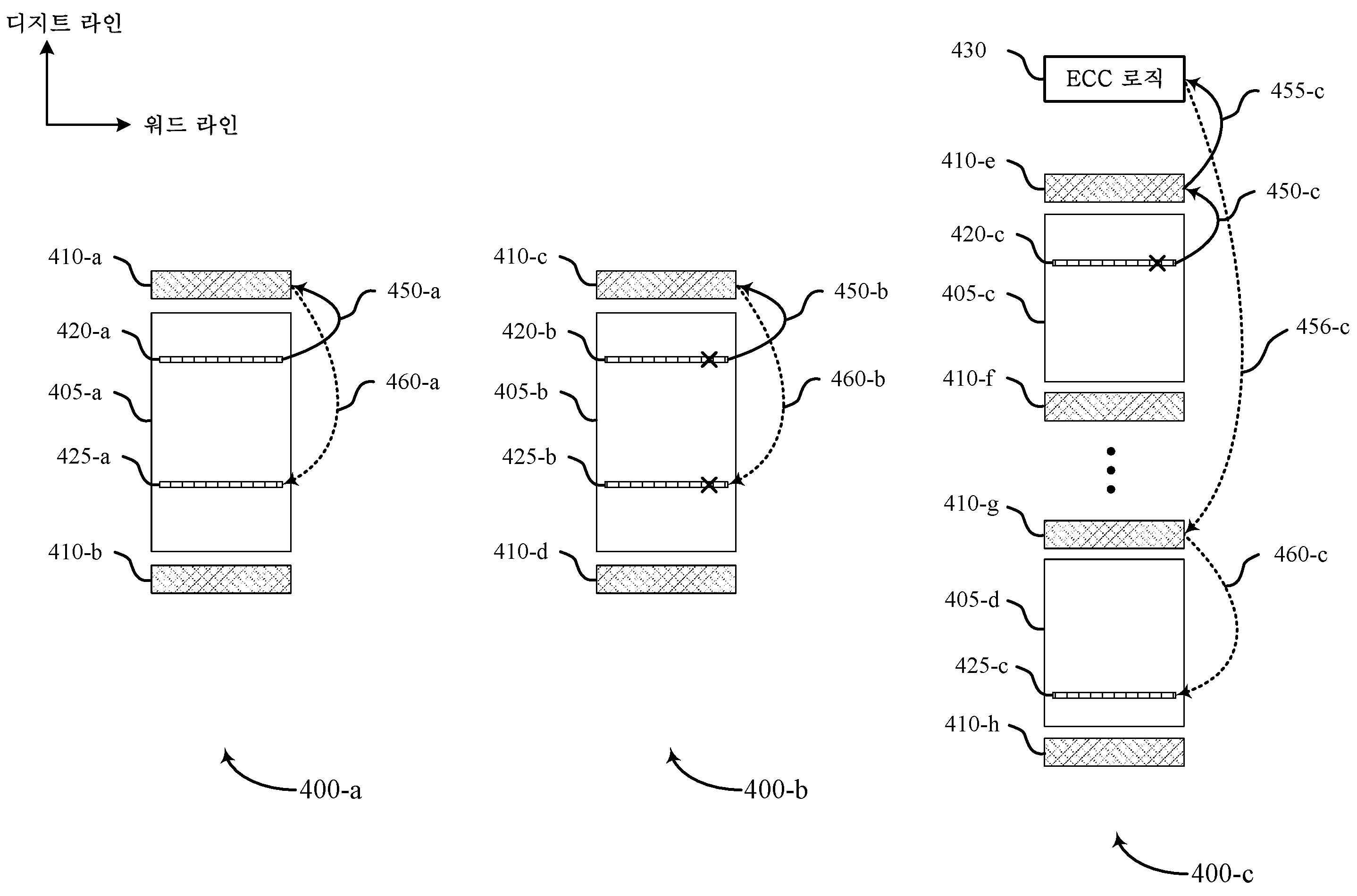
도 4는 본 개시의 실시 예들에 따른 랜덤 액세스 및 강유전체 메모리를 위한 웨어 레벨링을 지원하는 동작들의 도해들을 도시한다. 도해들(400)은 메모리 타일(405), 감지부(410), 소스 페이지(420), 대상 페이지(425) 및 오류 정정 코드(ECC) 로직(430)을 포함한다. 소스 페이지(420)와 대상 페이지(425)는 동일한 메모리 타일에 존재할 수도 존재하지 않을 수도 있다. 4 illustrates diagrams of operations supporting wear leveling for random access and ferroelectric memory according to embodiments of the present disclosure. The diagrams 400 include a
메모리 타일(405)은 다양한 수의 메모리 셀을 포함하도록 구성될 수 있다. 경우에 따라, 메모리 타일(405)은 2-차원 매트릭스로 배열된 1024 x 1024개의 메모리 셀을 포함할 수 있다. 메모리 타일의 다른 구성들, 예를 들어, 2048 x 2048 또는 1024 x 2048개의 메모리 셀도 가능할 수 있다. 경우에 따라, 메모리 타일(405)의 수평 배열은 메모리 어레이의 섹션으로 지칭될 수 있다(도시되지 않음). 경우에 따라, 수평 방향은 워드 라인 방향일 수 있다. 경우에 따라, 섹션들의 수직 배열(즉, 타일들의 2-차원 배열)은 메모리 어레이의 뱅크로 지칭될 수 있다(도시되지 않음). 경우에 따라, 수직 방향은 디지트 라인 방향일 수 있다.
감지부(410)는 감지 구성요소 및 래치를 포함할 수 있다. 감지부(410)의 감지 구성요소는 도 1 및 도 2를 참조하여 설명된 감지 구성요소(125)의 일례일 수 있다. 감지부(410)의 래치는 도 1 및 도 2를 참조하여 설명한 바와 같은 래치(127)의 일례일 수 있다. 경우에 따라, 감지부(410)는 메모리 어레이의 섹션과 연관될 수 있다. 일례로, 감지부(410-e)는 메모리 타일(405-c)과 연관된 섹션을 감지하도록 구성될 수 있고 메모리 어레이의 다른 섹션들(예를 들어, 메모리 타일(405-d))은 감지하도록 구성되지 않을 수 있다. 감지부(410)는 메모리 타일(405)의 일측 또는 양측에 수직 또는 디지트 라인 방향으로 위치될 수 있다.The
ECC 로직(430)은 메모리 어레이를 갖는 칩 상에 위치될 수 있다. ECC 로직(430)은 데이터 집합에 존재할 수 있는 특정 수의 오류를 검출 및 정정하도록 구성된 다양한 트랜지스터 및 다른 회로 요소를 포함할 수 있다. ECC 로직(430)은 메모리 어레이(예를 들어, 메모리 타일(405-c) 또는 메모리 타일(405-d))의 뱅크-레벨 로직의 임의의 섹션으로부터의 데이터 집합에 관해 ECC 기능을 수행하도록 구성될 수 있다. 경우에 따라, ECC 로직(430)은 데이터의 페이지로부터 데이터의 부분 집합에 관해 ECC 기능을 수행하도록 구성될 수 있다. ECC 로직(430)이 ECC 기능을 수행하는 데이터의 부분 집합은 코드-워드로 지칭될 수 있다.
도해(400-a 및 400-b)에 도시된 바와 같이, 소스 페이지(420) 및 대상 페이지(425)는 둘 다 동일한 타일(예를 들어, 메모리 타일(405-a 또는 405-b)), 그로 인해 메모리 어레이의 동일한 섹션(도시되지 않음) 내에 위치될 수 있다. 소스 페이지(420)는 메모리 셀들에 공통인 워드 라인과 연관된 메모리 셀들(즉,웨어 레벨링 동작 동안 데이터가 복사되는 메모리 셀들)을 포함할 수 있다. 경우에 따라, 소스 페이지(420)는 도 1 및 도 2를 참조하여 설명된 바와 같이 워드 라인에 연결되는 1024개의 메모리 셀의 로우를 포함할 수 있다. 1024개의 메모리 셀들의 각각은 도 1 및 도 2를 참조하여 설명된 바와 같이 감지부(410)에 연결될 수 있는 디지트 라인과 연관될 수 있다. 대상 페이지(425)는 메모리 셀들에 대해 공통으로 구성된 다른 워드 라인과 연관된 소스 페이지(예를 들어, 1024개의 메모리 셀의 로우)와 동일한 수의 메모리 셀(즉,웨어 레벨링 동작 동안 데이터가 복사되는 메모리 셀)을 포함할 수 있다. 소스 페이지(420)의 메모리 셀들 및 대상 페이지(425)의 메모리 셀들은 도 1 및 도 2를 참조하여 설명된 바와 같이 공통 비트 라인들과 연관될 수 있다.As shown in diagrams 400-a and 400-b,
도해(400-a)는 웨어 레벨링 동작 동안 수행되는 페이지 복사 동작의 일례를 도시할 수 있다. 소스 페이지(420-a)는 감지부(410-a 및/또는 410-b)에서 소스 페이지(420-a)에 저장된 데이터를 캡처하도록 활성화될 수 있다(즉, 소스 페이지(420-a)와 연관된 워드 라인 및 디지트 라인들이 선택 또는 턴 온된다). 데이터의 디코딩, 감지 및 캡처는 도 1 내지 도 3을 참조하여 상술된 바와 같은 절차들에 따라 수행될 수 있다. 소스 페이지(420-a)로부터 감지부(410-a)로의 데이터의 캡처는 경로(450-a)로 도시될 수 있다. 소스 페이지(420-a)로부터 감지부(410-b)로의 데이터 캡처는 도시의 간략화를 위해 생략된다.The diagram 400 - a may illustrate an example of a page copy operation performed during a wear leveling operation. The source page 420 - a may be activated by the sensing unit 410 - a and/or 410 - b to capture data stored in the source page 420 - a (ie, the source page 420 - a and the associated word line and digit lines are selected or turned on). Decoding, sensing and capturing of data may be performed according to procedures as described above with reference to FIGS. 1 to 3 . The capture of data from the source page 420 - a to the sensing unit 410 - a may be illustrated as a path 450 - a. Data capture from the source page 420 - a to the sensing unit 410 - b is omitted for simplicity of illustration.
예를 들어, 감지부(410-a 및/또는 410-b)에서 소스 페이지(420-a)로부터의 데이터의 캡처에 기초하여, 소스 페이지(420-a)와 연관된 워드 라인 및 디지트 라인들은 선택 해제 또는 턴 오프될 수 있다. 소스 페이지(420-a)와 연관된 워드 라인 및 디지트 라인들을 턴 오프하는 것에 기초하여, 대상 페이지(425-a)와 연관된 워드 라인 및 디지트 라인들은 선택 또는 턴 온될 수 있다. 대상 페이지(425-a)와 연관된 워드 라인 및 디지트 라인들을 턴 온하는 것, 즉 대상 페이지(425-a)가 인에이블되는 것에 기초하여, 감지부(410-a 및/또는 410-b)에서 저장 또는 캡처된 데이터가 대상 페이지(425-a)의 메모리 셀들에 기록될 수 있다. 경우에 따라, 감지부(410-a 및/또는 410-b)로부터 대상 페이지(425-a)로 데이터를 기록하는 것은 대상 페이지(425-a)를 사전 충전하는 것으로 지칭될 수 있다. 감지부(410-a)로부터 대상 페이지(425-a)로의 데이터의 기록, 즉 대상 페이지(425-a)의 사전 충전은 경로(460-a)로 도시될 수 있다. 감지부(410-b)로부터 대상 페이지(425-a)로의 데이터의 기록은 도시의 간략화를 위해 생략된다.For example, based on the capture of data from the source page 420 - a in the sensing unit 410 - a and/or 410 - b , the word lines and digit lines associated with the source page 420 - a are selected. It can be turned off or turned off. Based on turning off the word line and digit lines associated with the source page 420 - a, the word line and digit lines associated with the destination page 425 - a may be selected or turned on. Based on turning on the word line and digit lines associated with the target page 425-a, that is, the target page 425-a is enabled, the sensing unit 410-a and/or 410-b The stored or captured data may be written to memory cells of the target page 425 - a. In some cases, writing data from the sensing unit 410 - a and/or 410 - b to the target page 425 - a may be referred to as pre-charging the target page 425 - a . The writing of data from the sensing unit 410 - a to the target page 425 - a , ie, pre-charging of the target page 425 - a may be illustrated as a path 460 - a. The writing of data from the sensing unit 410 - b to the target page 425 - a is omitted for simplicity of illustration.
상술된 시퀀스는 웨어 레벨링 동작 동안 소스 페이지(420-a)로부터 대상 페이지(425-a)로 데이터를 이동시킬 수 있다. 감지부(410-a 및/또는 410-b)는 데이터의 이동 시퀀스를 용이하게 할 수 있다. 시퀀스는 특정 물리적 페이지(예를 들어, 소스 페이지(420-a))가 반복적으로 사이클링되는 것(예를 들어, 소스 페이지(420-a)의 메모리 셀들의 프로그래밍 및 소거)을, 다른 물리적 페이지(예를 들어, 대상 페이지(425-a)의 메모리 셀들)를 이용하여 웨어 레벨링 풀(예를 들어, 1024개의 상이한 물리적 페이지 위치)에서의 다수의 페이지에 걸쳐 사이클링 이벤트를 효율적으로 확산시킴으로써, 회피한다. 데이터의 논리적 주소는 데이터가 실제로 웨어 레벨링 풀 내에 존재하는 페이지의 물리적 위치에 관계없이 동일하게 유지될 수 있다. 소스 페이지(420-a)로부터 데이터를 캡처한 후에는 그것의 사전 충전이 없기 때문에, 소스 페이지(420-a)에 존재하는 데이터는 더 이상 유효하지 않거나 신뢰할 수 없다. 웨어-레벨링 적용시, 소스 페이지(420-a)는 새로운 예비 페이지, 즉 대상 페이지의 역할을 할 수 있는 메모리 페이지가 될 수 있다.The above-described sequence may move data from the source page 420 - a to the target page 425 - a during the wear leveling operation. The sensing unit 410 - a and/or 410 - b may facilitate a movement sequence of data. The sequence is that a particular physical page (e.g., source page 420-a) is cycled repeatedly (e.g., programming and erasing memory cells of source page 420-a) and another physical page (e.g., Avoid, e.g., by efficiently spreading a cycling event across multiple pages in a wear leveling pool (eg, 1024 different physical page locations) using the memory cells of the target page 425 - a). . The logical address of the data can remain the same regardless of the physical location of the page where the data actually resides within the wear leveling pool. Since there is no pre-filling of it after capturing data from the source page 420-a, the data present in the source page 420-a is no longer valid or unreliable. When wear-leveling is applied, the source page 420 - a may become a new spare page, that is, a memory page that can serve as a target page.
도해(400-a)에 도시된 바와 같이, 감지부(410-a 및/또는 410-b)를 이용하면 섹션 내에서의 웨어 레벨링 동작을 가능하게 할 수 있지만 감지부(410)가 섹션의 메모리 셀들 전용으로 구성되기 때문에 웨어 레벨링 풀이 섹션 내에 존재하는 페이지들(예를 들어, 1024개의 페이지) 중에 제한될 수 있다.As shown in the diagram 400-a, the use of the sensing units 410-a and/or 410-b may enable wear leveling operations within a section, but the
도해(400-b)는 소스 페이지(420-b)에 오류(들)가 존재할 수 있을 때 웨어-레벨링 동작 동안 상술된 시퀀스에 수반되는 데이터의 이동을 도시할 수 있다. 오류(들)는 결함이 있거나 잘못된 페이지의 메모리 셀(들)의 컨텐츠와 연관될 수 있다. 오류(들)는 도해(400-b)에서 심볼 X로 도시되어 있다. 웨어 레벨링 동작은 도해(400-a)를 참조하여 상술된 시퀀스와 동일한 시퀀스를 수반한다. 소스 페이지(420-b)로부터 감지부(410-c)로의 오류(들)를 포함하는 데이터의 캡처는 경로(450-b)로 도시될 수 있다. 감지부(410-c)로부터 대상 페이지(425-b)로의 오류(들)를 포함하는 데이터의 기록, 즉 대상 페이지(425-b)의 사전 충전은 경로(460-b)로 도시될 수 있다. 도해(400-b)의 예에서, 오류(들)는 소스 페이지(420-b)로부터 대상 페이지(425-b)로 데이터의 일부로서 복사될 수 있다. 그러한 오류의 전파는 대상 페이지(425-b)가 결함이 있거나 잘못된 메모리 셀(들)로 인해 자체 오류(들)를 가질 수 있기 때문에 대상 페이지(425-b)와 연관된 오류 정정 성능을 소비할 수 있다. 오류 정정 동작은 소스 페이지(420-b)의 컨텐츠를 대상 페이지(425-b)에 저장하기 전에 소스 페이지(420-b)에서 결함이 있거나 잘못된 메모리 셀(들)의 컨텐츠를 정정했을 수 있다.The diagram 400 - b may illustrate the movement of data that accompanies the above-described sequence during a wear-leveling operation when an error(s) may exist in the source page 420 - b . The error(s) may be associated with the contents of the memory cell(s) of a defective or erroneous page. The error(s) are shown by symbol X in diagram 400-b. The wear leveling operation involves the same sequence as the sequence described above with reference to the diagram 400 - a. The capture of data including error(s) from the source page 420 - b to the sensing unit 410 - c may be illustrated by path 450 - b . The writing of data including error(s) from the sensing unit 410 - c to the target page 425 - b , ie, pre-charging of the target page 425 - b , may be illustrated by a path 460 - b . . In the example of diagram 400 - b , the error(s) may be copied as part of the data from source page 420 - b to destination page 425 - b . Propagation of such errors may consume error correction performance associated with destination page 425-b as destination page 425-b may have its own error(s) due to defective or faulty memory cell(s). have. The error correction operation may correct the contents of defective or incorrect memory cell(s) in the source page 420 - b before storing the contents of the source page 420 - b in the target page 425 - b .
도해(400-c)는 심볼 X로 표기된 바와 같이, 소스 페이지(420-c)에 존재할 수 있는 오류(들)를 정정하기 위해 ECC 로직(430)과 함께 웨어 레벨링 동작 동안 다른 시퀀스에 수반되는 데이터의 이동을 도시할 수 있다. 소스 페이지(420-c)로부터의 오류(들)를 포함하는 데이터가 경로(450-c)로 표기된 바와 같이, 감지부(410-e)에서 감지 및 캡처된 후, 소스 페이지(420-c)로부터의 데이터의 부분 집합이 차례로, 감지부(410-e)로부터 ECC 로직(430)으로 송신되고 ECC 로직(430)에 의해 "스크러빙(scrubbing)"될 수 있다. 경우에 따라, 부분 집합은 코드-워드(예를 들어, 페이지의 일부)일 수 있다. 스크러빙은 경로(455-c)로 표기된 바와 같이, ECC 로직(430)을 통해 각 코드-워드를 처리하고 코드-워드에 존재할 수 있는 오류들을 정정하는 것을 의미할 수 있다. 예로서, 페이지당 여덟(8) 개의 코드-워드가 있다면, 각 코드-워드는 감지부(410-e)로부터 나와, ECC 로직(430)을 통해 처리될 수 있다. 그로 인해, ECC 로직(430)을 통해 ECC 기능을 수행하는 시퀀스의 이러한 부분은 여덟 개의 시퀀스 또는 동작의 루프로 수행될 수 있다.Illustrated 400-c shows data accompanying another sequence during a wear leveling operation in conjunction with
감지부(410-e)에서 캡처된 데이터를 스크러빙하는 것은 ECC 로직(430)을 통해 각 코드-워드를 처리하는 것을 수반할 수 있다. 이는 메모리 어레이의 뱅크-레벨 로직에 존재할 수 있는 ECC 로직(430)에 도달하기 위해 섹션 레벨을 넘어서는 데이터 트래픽 동작들로 인해 도해들(400-a 및 400-b)에 도시된 바와 같이 소스 페이지(420) 및 대상 페이지(425)를 동일한 섹션(예를 들어, 타일(405)) 내에 유지하는 것과 연관된 이점들을 제한할 수 있다. 그러나, 웨어 레벨링 풀이 클수록 웨어 레벨링이 더 효율적일 수 있기 때문에 상이한 섹션들에 걸쳐 페이지 복사 동작이 이루어질 때 웨어 레벨링 풀의 크기가 증가될 수 있다. 따라서, ECC 로직(430)을 통해 각 코드-워드를 처리함으로써 스크러빙이 수행될 수 있으면서, ECC 로직(430)에 의해 스크러빙된 각 코드-워드는 경로(456-c)로 표기된 바와 같이 타일(405-d)과 연관된 감지부(410-g)에 저장될 수 있다.Scrubbing the captured data in the sensing unit 410 - e may involve processing each code-word via the
타일(405-d)은 대상 페이지(425-c)를 포함하는 상이한 타일이고 감지부(410-g 또는 410-h)와 연관될 수 있다. 그 후, ECC 로직(430)에 의해 스크러빙된 감지부(410-g)의 데이터는 경로(460-c)로 표기된 바와 같이, 타일(405-d)의 대상 페이지(425-c)에 저장될 수 있다. 결과적으로, ECC 로직(430)을 통해 오류가 정정된 소스 페이지(420-c)의 컨텐츠는 메모리 어레이의 상이한 섹션에 존재할 수 있는 대상 페이지(425-c)로 전달될 수 있다. ECC 로직(430)에 의해 수행된 오류 정정 기능으로 인해, 대상 페이지(425-c)에 심볼 X가 없는 것으로 표기된 바와 같이, 대상 페이지(425-c)에 저장되는 데이터의 컨텐츠에는 오류가 없을 수 있다. 본 개시의 실시 예들에 따른 도해(400-c)을 참조하여 설명된 바와 같은 웨어 레벨링 동작들의 보다 세부 사항들은 도 5a 및 도 5b에서 후술된다.The tile 405 - d is a different tile including the target page 425 - c and may be associated with the sensing unit 410 - g or 410 - h. Thereafter, the data of the sensing unit 410 - g scrubbed by the
도 5a 및 도 5b는 본 개시의 실시 예들에 따른 랜덤 액세스 및 강유전체 메모리를 위한 웨어 레벨링을 지원하는 동작들의 도시한다. 도해(500)는 메모리 타일들(505), 감지부들(510), 소스 페이지(520), 대상 페이지(525) 및 ECC 로직(530)을 포함한다. 5A and 5B illustrate operations supporting wear leveling for random access and ferroelectric memory according to embodiments of the present disclosure. The diagram 500 includes
메모리 타일들(505)은 도 4를 참조하여 설명된 바와 같은 메모리 타일들(405)의 일례일 수 있다. 상술된 바와 같이, 경우에 따라, 메모리 타일들(505)의 수평 배열은 메모리 어레이의 섹션으로 지칭될 수 있다(도시되지 않음). 경우에 따라, 수평 방향은 워드 라인 방향일 수 있다. 경우에 따라, 섹션들의 수직 배열(즉, 타일들의 2-차원 배열)은 메모리 어레이의 뱅크로 지칭될 수 있다. 경우에 따라, 수직 방향은 디지트 라인 방향일 수 있다. 도 5a 및 도 5b를 참조하여 설명된 시퀀스가 메모리 어레이의 동일한 섹션 내의 소스 및 대상 페이지들로 제한되지 않을 수 있기 때문에 메모리 어레이의 섹션으로부터 다른 섹션으로 데이터를 이동하는 것을 도시하기 위해 다수의 메모리 타일(505)이 도 5a 및 도 5b에 도시되어 있다.The
감지부(510)는 도 4를 참조하여 설명된 바와 같은 감지부(410)의 일례일 수 있다. 경우에 따라, 감지부(510-a 및/또는 510-b)는 감지부(510-a 및/또는 510-b)가 505-b, 505-c 또는 505-d와 같은 메모리 어레이의 상이한 섹션의 다른 타일들을 감지하는 데 이용되지 않을 수 있도록 메모리 어레이의 타일(505-a)(또는 타일(505-a)을 포함하는 섹션, 도시되지 않음)과 연관될 수 있다. 감지부들(510)은 도 4를 참조하여 상술된 바와 같이, 메모리 타일들(505)의 일측 또는 양측에 수직 또는 디지트 라인 방향으로 위치될 수 있다.The
ECC 로직(530)은 도 4를 참조하여 설명된 바와 같은 ECC 로직(430)의 일례일 수 있다. ECC 로직(530)은 메모리 어레이의 뱅크-레벨 내 임의의 섹션들로부터의 데이터 집합들에 대한 ECC 기능을 수행하도록 구성될 수 있다. 그로 인해, ECC 로직(530)은 타일들(505-a, 505-b, 505-c 또는 505-d)로부터의 데이터 집합에 대한 ECC 기능을 수행할 수 있다.The
도해(500-a)의 단계 1은 활성화(ACT) 단계를 나타낼 수 있다. ACT 단계 동안, 소스 페이지(520-a)는 감지부(510-a 및/또는 510-b)에서 소스 페이지(520-a)에 저장된 데이터를 감지 및 캡처하도록 활성화될 수 있다(즉, 소스 페이지(520-a)와 연관된 워드 라인 및 디지트 라인들이 선택 또는 턴 온된다). 소스 페이지(520-a)의 심볼 X는 소스 페이지(520-a)의 데이터의 컨텐츠에 존재하는 오류(들)를 나타낼 수 있다. 소스 페이지(520-a)로부터 감지부(510-a 및/또는 510-b)로의 데이터의 캡처는 경로(550-a 및/또는 550-b)로 도시될 수 있다.
도해(500-a)의 단계 2는 유지(HOLD) 단계를 나타낼 수 있다. 유지 단계 동안, 감지부(510-a 및 510-b)의 감지 구성요소들은 셧 다운(shut down)될 수 있다. 또한, 소스 페이지(520-a)로부터의 데이터가 여전히 감지부(510-a 및 510-b)의 래치들에 유지될 수 있는 것을 제외하고, 워드 라인들 및 디지트 라인들에 대한 선택 회로 및 메모리 어레이와 연관된 다른 제어 회로들이 비활성화될 수 있다. 그로 인해, 유지 단계는 감지부(510-a 및 510-b)의 래치들이 그 안에 데이터를 보유할 수 있는 것을 제외하고는 유휴 상태로 보여질 수 있다. 감지부(510-b)의 심볼 X는 소스 페이지(520-a)로부터 전파된 데이터의 컨텐츠에 존재하는 오류(들)를 나타낼 수 있다. 또한, 소스 페이지(520-a)의 데이터는 그 안에서 데이터를 사전 충전하지 않기 때문에 더 이상 유효하거나 신뢰할 수 없다. 상술된 바와 같이, 소스 페이지(520-a)는 웨어 레벨링 적용 동안 새로운 예비 페이지, 즉 대상 페이지의 역할을 할 수 있는 메모리 페이지가 될 수 있다.Step 2 of the diagram 500 - a may represent a HOLD phase. During the maintenance phase, the sensing components of the sensing units 510 - a and 510 - b may be shut down. Also, select circuitry and memory for word lines and digit lines, except that data from source page 520 - a may still be held in latches of sense units 510 - a and 510 - b . Other control circuits associated with the array may be deactivated. As such, the holding phase may be viewed as idle except that the latches of the sensing units 510-a and 510-b may hold data therein. The symbol X of the sensing unit 510 - b may indicate error(s) existing in content of data propagated from the source page 520 - a. Also, the data in the source page 520 - a is no longer valid or reliable because it does not pre-fill the data therein. As described above, the source page 520 - a may be a new spare page, that is, a memory page that may serve as a target page during wear leveling application.
도해(500-a)의 단계 3은 사전 설정(Pre-Set) 단계를 나타낼 수 있다. 사전 설정 단계 동안, 상이한 섹션에 위치된 타일인 타일(555-d)의 대상 페이지(525-a)의 일부 또는 모든 메모리 셀은 특정 로직 상태로 프로그래밍될 수 있다. 경우에 따라, 로직 상태는 로직 1에 대응할 수 있다. 대상 페이지(525-a)는 소스 페이지(520-a)가 위치되는 타일(또는 섹션)과 상이한 타일(또는 섹션)에 존재함으로써, 웨어 레벨링 풀 크기를 확장할 수 있는 것으로 이해되어야 한다. 사전 설정 단계 동안, 대상 페이지(525-a)와 연관된 ISO 디바이스들은 비활성화될 수 있다. 도 2를 참조하여 상술된 바와 같이, ISO 디바이스는 비활성화될 때, 감지 구성요소들의 디지트 라인 노드들을 메모리 어레이의 디지트 라인들로부터 분리할 수 있다. 대상 페이지(525-a)와 연관된 ISO 디바이스들이 비활성화되는 동안 대상 페이지(525-a)의 메모리 셀들은 단일 로직 상태로 사전 기록될 수 있다. 경우에 따라, 사전 기록된 로직 상태는 1의 로직 상태에 대응할 수 있다.Step 3 of the diagram 500 - a may represent a preset (Pre-Set) step. During the preset phase, some or all of the memory cells of the target page 525 - a of the tile 555 - d, which are tiles located in different sections, may be programmed to a particular logic state. In some cases, the logic state may correspond to a logic one. It should be understood that the target page 525 - a may extend the wear leveling pool size by being in a tile (or section) different from the tile (or section) in which the source page 520 - a is located. During the preset phase, ISO devices associated with the target page 525 - a may be deactivated. As described above with reference to FIG. 2 , the ISO device, when deactivated, may isolate the digit line nodes of the sense components from the digit lines of the memory array. Memory cells of target page 525 - a may be pre-written to a single logic state while ISO devices associated with target page 525 - a are deactivated. In some cases, the pre-written logic state may correspond to a logic state of 1.
도 4b의 도해(500-b)의 단계 4는 소스 페이지(520-a)의 컨텐츠를 스크러빙하기 위해 ECC 로직(530)을 통해 감지부(510-a 및/또는 510-b)의 래치들에 저장된 소스 페이지(520-a)의 모든 코드-워드를 통한 처리 동작을 나타낼 수 있다. 감지부(510-a 및/또는 510-b)로부터 ECC 로직(530)으로 코드-워드들을 전송함으로써 그것들을 스크러빙하는 것은 경로들(555-a 및/또는 555-b)로서 도시될 수 있다. 각 코드-워드는 대상 페이지(525-a)와 연관된 감지부(510-c 및/또는 510-d)의 래치들에 저장될 수 있다. ECC 로직(530)으로부터 감지부(510-c 및/또는 510-d)의 래치로의 코드-워드들의 저장은 경로들(560-a 및/또는 560-b)로서 도시될 수 있다. 대상 페이지(525-a)와 연관된 감지부(510-c 및/또는 510-d)에 저장된 데이터의 컨텐츠에 심볼 X가 없는 것은 ECC 기능을 수행하는 ECC 로직(530)으로 인해 데이터에 소스 페이지(520-a)의 컨텐츠의 오류(들)가 없다는 것을 나타낸다.Step 4 of the diagram 500-b of FIG. 4B connects the latches of the sensing unit 510-a and/or 510-b via the
단계 4에서의 동작들은 단계 3에서의 동작들과 동시에 수행될 수 있는 것으로 이해되어야 한다. 타일(505-d)과 연관된 ISO 디바이스들은 비활성화될 때, 감지부(510-c 및/또는 510-d)를 타일(505-d)의 메모리 셀들, 그로 인해 대상 페이지(525-a)의 메모리 셀들로부터 분리시킨다. 단계 3 및 단계 4에서의 동작들은 단계 3에서의 동작들(예를 들어, 대상 페이지(525-a)의 메모리 셀들에 대한 사전 설정 단계)이 비활성화된 ISO 디바이스들로 인해 단계 4에서의 동작들(예를 들어, ECC 로직을 통한 코드-워드들의 처리 및 감지부(510-c 및/또는 510-d)의 래치들에의 스크러빙된 코드-워드들의 저장)에서 독립적일 수 있기 때문에 동시에 수행될 수 있다. 단계 3 및 단계 4의 동시 병행 동작은 웨어 레벨링 동작과 연관된 전체 시간을 감소시킬(또는 적어도 부분적으로 "숨길") 수 있다.It should be understood that the operations in step 4 may be performed concurrently with the operations in step 3 . When the ISO devices associated with the tile 505-d are deactivated, the sensing unit 510-c and/or 510-d transfers the memory cells of the tile 505-d, thereby the memory of the target page 525-a. separate from the cells. The operations in Step 3 and Step 4 are the operations in Step 4 due to ISO devices in which the operations in Step 3 (eg, a preset step for memory cells of the target page 525 - a) are deactivated. (e.g., processing of code-words via ECC logic and storage of scrubbed code-words in latches of sensing unit 510-c and/or 510-d) can The concurrent concurrent operation of steps 3 and 4 may reduce (or at least partially “hide”) the overall time associated with the wear leveling operation.
도해(500-b)의 단계 5는 소스 페이지(520-a)를 사전 충전하지 않는 감지부(510-a 및/또는 510-b)의 래치들의 폐쇄와 연관된 동작들을 나타낼 수 있다. 단계 5의 완료, 즉 감지부(510-a 및/또는 510-b)의 래치들의 폐쇄시, 감지부(510-a 및/또는 510-b)는 더 이상 소스 페이지(520-a)로부터의 유효 데이터를 나타내지 않는다. 또한, 소스 페이지(520-a)가 웨어 레벨링 동작 동안 예비 페이지로서 의 역할을 할 수 있기 때문에 할 수 있기 때문에 소스 페이지(520-a)의 사전 충전은 필요하지 않을 수 있다. 소스 페이지(520-a)의 사전 충전 생략은 웨어 레벨링 적용과 연관된 전체 시간 및 에너지를 감소시킬 수 있다.Step 5 of the diagram 500 - b may represent operations associated with closing the latches of the sensing units 510 - a and/or 510 - b that do not pre-fill the source page 520 - a. Upon completion of step 5, i.e., closing of the latches of sensing unit 510-a and/or 510-b, sensing unit 510-a and/or 510-b no longer releases from source page 520-a. Does not represent valid data. Also, since the source page 520 - a may serve as a spare page during the wear leveling operation, pre-charging of the source page 520 - a may not be necessary. Omitting the pre-charging of the source page 520 - a may reduce the overall time and energy associated with applying wear leveling.
도해(500-b)의 단계 6은 감지부(510-c 및/또는 510-d)에 저장된 데이터를 기록 대상 페이지(525-a)에 기록하는 것을 나타낼 수 있다. 경우에 따라, 대상 페이지(525-a)에 기록하는 것은 대상 페이지(525-a)를 사전 충전하는 것으로 지칭될 수 있다. 감지부(510-c 및/또는 510-d)로부터 대상 페이지(525-a)로 데이터를 사전 충전하는 것은 경로(565-a 및/또는 565-b)로 도시될 수 있다. 대상 페이지(525-a)에 데이터를 사전 충전하는 것은 상술된 바와 같이 단계 3에서 설정된 사전 기록된 로직 상태와 상이한 로직 상태를 저장하는 대상 페이지(525-a)의 메모리 셀들에만 데이터의 부분 집합을 기록하는 것은 포함할 수 있는 것으로 이해되어야 한다. 예를 들어, 단지 메모리 셀들이 로직 상태 "1"로 사전 기록될 때 로직 "0"을 저장하기 위한 대상 페이지(525-a)의 메모리 셀들만 논리 "0"으로 프로그래밍될 필요가 있을 수 있다. 대상 페이지(525-a)를 사전 충전하는 동안 메모리 셀들의 수를 감소시키는 것은 웨어 레벨링 적용과 연관된 전체 시간 및 에너지를 감소시킬 수 있다.Step 6 of the diagram 500 - b may represent writing the data stored in the sensing units 510 - c and/or 510 - d to the recording target page 525 - a . In some cases, writing to the target page 525 - a may be referred to as pre-filling the target page 525 - a . The pre-charging of data from the sensing unit 510 - c and/or 510 - d to the target page 525 - a may be illustrated by paths 565 - a and/or 565 - b . Pre-charging data into target page 525-a only sub-sets the data to memory cells of target page 525-a that store a logic state different from the pre-written logic state set in step 3 as described above. It should be understood that recording may include. For example, only the memory cells of target page 525 - a to store a logic “0” may need to be programmed to a logic “0” when the memory cells are pre-written to a logic state “1”. Reducing the number of memory cells while pre-charging the target page 525 - a may reduce the overall time and energy associated with applying wear leveling.
도 5a 및 도 5b를 참조하여 상술된 단계 1 내지 단계 6은 소스 및 대상 페이지들 둘 다가 메모리 어레이의 동일한 섹션 내에 있어야 하는 제한을 회피함으로써 더 큰 웨어 레벨링 풀 크기로 웨어 레벨링을 가능하게 한다. 또한, 오류 정정이 오류 전파 문제로 인한 대상 페이지의 오류 정정 용량의 소비를 회피하기 위해 소스 페이지의 컨텐츠를 스크러빙하도록 수행될 수 있다. 또한, 효율적인 웨어 레벨링 동작을 실현하기 위한 전체 시간 및 에너지 소비가 감소될 수 있다.
도 6은 본 개시의 실시 예들에 따른 랜덤 액세스 및 강유전체 메모리를 위한 웨어 레벨링을 지원하는 메모리 디바이스(100-a)의 블록도(600)를 도시한다. 메모리 디바이스(100-a)는 전자 메모리 장치로 지칭될 수 있고 메모리 제어기(140-a) 및 메모리 셀들(105-b)을 포함하며, 이것들은 도 1을 참조하여 설명된 메모리 제어기(140) 및 메모리 셀(105)의 예들일 수 있다. 메모리 제어기(140-a)는 메모리 셀들(105-b)의 어레이와 동일한 기판 상에 존재하는 내부 로직 회로일 수 있다. 또한 메모리 제어기(140-a)는 본 개시의 실시 예들에 따른 웨어 레벨링 동작 동안 ECC 로직과 함께 웨어 레벨링 및 ECC 기능과 연관된 동작들을 제어할 수 있다. 메모리 제어기(140-a)는 바이어싱 구성요소(610) 및 타이밍 구성요소(615)를 포함할 수 있고 도 1을 참조하여 설명된 바와 같이 메모리 디바이스(100-a)를 동작시킬 수 있다. 메모리 제어기(140-a)는 워드 라인(110-b), 플레이트 라인(210-a) 및 감지 구성요소(125-b)와 전자 통신할 수 있으며, 이것들은 도 1 및 도 2를 참조하여 설명된 워드 라인(110), 디지트 라인(115), 플레이트 라인(210) 및 감지 구성요소(125)의 예들일 수 있다. 6 is a block diagram 600 of a memory device 100 - a supporting wear leveling for random access and ferroelectric memory according to embodiments of the present disclosure. The memory device 100 - a may be referred to as an electronic memory device and includes a memory controller 140 - a and memory cells 105 - b , which include the
또한 메모리 디바이스(100-a)는 기준 구성요소(620), 래치(625) 및 ECC 로직(630)을 포함할 수 있다. 감지부(640)는 감지 구성요소(125-b) 및 래치(625)를 포함할 수 있다. 래치(625)는 도 1 및 도 2를 참조하여 설명된 래치(127)의 일례일 수 있다. 또한, 메모리 디바이스(100-a)는 도 2를 참조하여 설명된 ISO 디바이스(295)의 일례일 수 있는 ISO 디바이스(695)를 포함할 수 있다. 본 개시의 실시 예들에 따른 웨어 레벨링 동작 동안, ISO 디바이스(695)는 감지 구성요소(125-b)의 디지트 라인 노드들을 메모리 셀(105-b)의 디지트 라인(DL)으로부터 분리시킬 수 있다. ISO 디바이스(695)는 본 개시의 실시 예들에 따라 도 5a 및 도 5b를 참조하여 상술된 바와 같이 단계 3 및 단계 4의 동시 실행을 가능하게 한다. 메모리 디바이스(100-a)의 구성요소들은 서로 전자 통신할 수 있고 도 1 내지 도 5를 참조하여 설명된 기능들을 수행할 수 있다. 경우에 따라, 기준 구성요소(620), 감지 구성요소(125-b) 및 래치(625)는 메모리 제어기(140-a)의 구성요소들일 수 있다.The memory device 100 - a may also include a
메모리 제어기(140-a)는 그러한 다양한 노드에 전압들을 인가함으로써 워드 라인(110-b), 플레이트 라인(210-a) 또는 디지트 라인(115-b)을 활성화시키도록 구성될 수 있다. 예를 들어, 바이어싱 구성요소(610)는 상술된 바와 같이 메모리 셀(105-b)을 동작시켜 메모리 셀(105-b)을 판독, 기록 또는 사전 충전하기 위해 전압을 인가하도록 구성될 수 있다. 경우에 따라, 메모리 제어기(140-a)는 도 1을 참조하여 설명된 바와 같이, 로우 디코더, 컬럼 디코더 또는 둘 다를 포함할 수 있다. 이는 메모리 제어기(140-a)가 하나 이상의 메모리 셀(105-c)에 액세스할 수 있게 할 수 있다. 또한 바이어싱 구성요소(610)는 감지 구성요소(125-b)에 대한 기준 신호를 생성하기 위해 기준 구성요소(620)에 전압 전위들을 제공할 수 있다. 또한, 바이어싱 구성요소(610)는 감지 구성요소(125-b)의 동작을 위한 전압 전위들을 제공할 수도 있다.Memory controller 140 - a may be configured to activate word line 110 - b , plate line 210 - a or digit line 115 - b by applying voltages to such various nodes. For example, the
경우에 따라, 메모리 제어기(140-a)는 타이밍 구성요소(615)를 사용하여 그것의 동작들을 수행할 수 있다. 예를 들어, 타이밍 구성요소(615)는 본 출원에서 논의된 판독, 기록 또는 사전 충전과 같은 메모리 기능들을 수행하기 위한 스위칭 및 전압 인가를 위한 타이밍을 비롯하여, 다양한 워드 라인 선택 또는 플레이트 라인 바이어싱의 타이밍을 제어할 수 있다. 경우에 따라, 타이밍 구성요소(615)는 바이어싱 구성요소(610)의 동작들을 제어할 수 있다.Optionally, memory controller 140 - a may use
기준 구성요소(620)는 감지 구성요소(125-b)에 대한 참조 신호를 생성하기 위한 다양한 구성요소를 포함할 수 있다. 기준 구성요소(620)는 참조 신호들을 생성하도록 구성된 회로를 포함할 수 있다. 경우에 따라, 기준 구성요소(620)는 다른 강유전체 메모리 셀들(105)을 포함할 수 있다. 일부 예에서, 기준 구성요소(620)는 도 3을 참조하여 설명된 바와 같이, 두 개의 감지 전압 간 값을 갖는 전압을 출력하도록 구성될 수 있다. 또는 기준 구성요소(620)는 가상 접지 전압(즉, 대략 0V)을 출력하도록 설계될 수 있다.The
감지 구성요소(125-b)는 메모리 셀(105-b)로부터의 신호(디지트 라인(115-b)를 통한)를 기준 구성요소(620)로부터의 기준 신호와 비교할 수 있다. 로직 상태를 결정시, 그 다음 감지 구성요소는 메모리 디바이스(100-a)가 일부인 전자 디바이스의 동작들에 따라 사용될 수 있는 래치(625)에 출력을 저장할 수 있다.Sense component 125 - b may compare the signal from memory cell 105 - b (via digit line 115 - b ) to a reference signal from
경우에 따라, 전자 메모리 디바이스는 강유전체 메모리 셀들의 복수의 섹션을 포함하는 메모리 어레이로서, 상기 복수의 섹션의 각 섹션은 감지 구성요소 집합 및 래치 집합과 연관되는, 상기 메모리 어레이, 상기 메모리 어레이 외측 주변의 오류 정정 회로, 및 상기 메모리 어레이, 상기 감지 구성요소 집합, 상기 래치 집합 및 상기 오류 정정 회로와 전자 통신하는 제어기를 포함할 수 있으며, 상기 제어기는 상기 메모리 어레이의 제1 섹션과 연관된 제1 래치 집합이 상기 메모리 어레이의 상기 제1 섹션으로부터 제1 데이터 집합을 수신하게 하도록, 상기 오류 정정 회로를 통해 상기 메모리 어레이의 제2 섹션과 연관된 제2 래치 집합으로 상기 제1 데이터 집합을 송신하게 하도록, 그리고 상기 오류 정정 회로를 통해 상기 메모리 어레이의 제2 섹션과 연관된 제2 래치 집합으로 상기 제1 데이터 집합을 송신하게 하도록, 그리고 상기 메모리 어레이의 상기 제2 섹션에 상기 제1 데이터 집합을 저장하게 하도록 작동 가능할 수 있다.Optionally, the electronic memory device is a memory array comprising a plurality of sections of ferroelectric memory cells, each section of the plurality of sections associated with a set of sensing elements and a set of latches; an error correction circuit, and a controller in electronic communication with the memory array, the set of sense components, the set of latches, and the error correction circuit, the controller comprising a first set of latches associated with a first section of the memory array receive a first set of data from the first section of the memory array, transmit the first set of data via the error correction circuitry to a second set of latches associated with a second section of the memory array; and transmit the first set of data to a second set of latches associated with a second section of the memory array through the error correction circuitry, and store the first set of data in the second section of the memory array. It may be possible.
경우에 따라, 상기 제어기는 상기 제1 섹션의 상기 제1 데이터 집합에 대응하는 메모리 셀들의 로우를 활성화시키도록, 상기 제1 섹션과 연관된 제1 감지 구성요소 집합을 사용하여 활성화된 상기 메모리 셀들의 로우로부터 상기 제1 데이터 집합을 감지하도록, 그리고 상기 제1 래치 집합에 상기 제1 데이터 집합을 저장하도록 작동 가능할 수 있다. 경우에 따라, 상기 제어기는 상기 제1 래치 집합에 상기 제1 데이터 집합을 유지시키면서 상기 제1 섹션의 상기 메모리 셀들의 로우를 비활성화시키도록 작동 가능할 수 있다. 경우에 따라, 상기 제어기는 상기 제2 섹션과 연관된 분리 디바이스들을 비활성화하는 것에 기초하여 상기 메모리 어레이의 상기 제2 섹션의 메모리 셀들을 분리시키도록, 그리고 분리된 상기 제2 섹션의 상기 메모리 셀들의 로우를 제1 로직 상태로 사전 기록하도록 작동 가능할 수 있다.Optionally, the controller is configured to activate a row of memory cells that are activated using a first set of sensing components associated with the first section to activate a row of memory cells corresponding to the first set of data in the first section. be operable to sense the first set of data from a row and to store the first set of data in the first set of latches. Optionally, the controller may be operable to deactivate the row of the memory cells of the first section while maintaining the first set of data in the first set of latches. Optionally, the controller is configured to detach the memory cells of the second section of the memory array based on deactivating isolation devices associated with the second section, and to detach the row of the memory cells of the second section that are separated. may be operable to pre-write to the first logic state.
경우에 따라, 상기 제어기는 상기 제1 데이터 집합을 상기 제1 래치 집합으로부터 상기 오류 정정 회로로 전달하도록, 상기 오류 정정 회로가 상기 제1 데이터 집합에 관해 오류 정정을 수행하게 하도록, 그리고 상기 오류 정정 회로로부터 상기 제2 래치 집합으로 상기 제1 데이터 집합을 전달하도록 작동 가능할 수 있다. 경우에 따라, 상기 제어기는 상기 제1 데이터 집합을 복수의 데이터 부분 집합으로 나누도록 그리고 상기 복수의 데이터 부분 집합의 각 부분 집합을 상기 오류 정정 회로를 통해 순차적으로 상기 제2 래치 집합으로 송신하도록 작동 가능할 수 있다.Optionally, the controller passes the first data set from the first set of latches to the error correction circuitry, causes the error correction circuitry to perform error correction on the first data set, and the error correction may be operable to pass the first set of data from circuitry to the second set of latches. Optionally, the controller is operative to divide the first data set into a plurality of data subsets and to transmit each subset of the plurality of data subsets to the second set of latches sequentially through the error correction circuitry. It may be possible.
경우에 따라, 상기 제어기는 동시에 상기 제1 데이터 집합을 송신하고 상기 제2 섹션의 분리된 상기 메모리 셀들의 로우를 사전 기록하도록 작동 가능할 수 있다. 경우에 따라, 상기 제어기는 상기 메모리 어레이의 상기 제1 섹션의 상기 로우를 사전 충전하지 않고 상기 제1 래치 집합을 폐쇄시키도록 작동 가능할 수 있다. 경우에 따라, 상기 제어기는 상기 제2 래치 집합에서의 상기 제1 데이터 집합으로 사전 기록된 상기 메모리 어레이의 상기 제2 섹션의 로우를 사전 충전하도록 작동 가능할 수 있다.Optionally, the controller may be operable to simultaneously transmit the first data set and pre-write the separated rows of memory cells in the second section. Optionally, the controller may be operable to close the first set of latches without pre-charging the row of the first section of the memory array. Optionally, the controller may be operable to pre-charge rows of the second section of the memory array that have been pre-written with the first set of data in the second set of latches.
일부 실시 예에서, 장치가 설명된다. 상기 장치는 메모리 어레이의 제1 섹션과 연관된 제1 래치 집합이 상기 메모리 어레이의 상기 제1 섹션으로부터 제1 데이터 집합을 수신하게 하는 수단, 오류 정정 회로를 통해 상기 메모리 어레이의 제2 섹션과 연관된 제2 래치 집합으로 상기 제1 데이터 집합을 송신하는 수단, 및 상기 메모리 어레이의 상기 제2 섹션에 상기 제1 데이터 집합을 수단을 포함할 수 있다. 경우에 따라, 상기 장치는 상기 제1 섹션의 상기 제1 데이터 집합에 대응하는 메모리 셀들의 로우를 활성화시키는 수단, 상기 제1 섹션과 연관된 제1 감지 구성요소 집합을 사용하여 활성화된 상기 메모리 셀들의 로우로부터 상기 제1 데이터 집합을 감지하는 수단, 및 상기 제1 래치 집합에 상기 제1 데이터 집합을 저장하는 수단을 더 포함할 수 있다. 경우에 따라, 상기 장치는 상기 제1 래치 집합에 상기 제1 데이터 집합을 유지시키면서 상기 제1 섹션의 상기 메모리 셀들의 로우를 비활성화시키는 수단을 더 포함할 수 있다.In some embodiments, an apparatus is described. The apparatus includes means for causing a first set of latches associated with a first section of a memory array to receive a first set of data from the first section of the memory array, a second set of latches associated with a second section of the memory array via an error correction circuit means for transmitting the first set of data in two sets of latches; and means for sending the first set of data to the second section of the memory array. Optionally, the device comprises means for activating a row of memory cells corresponding to the first data set of the first section, the memory cells activated using a first set of sensing components associated with the first section. The method may further include means for sensing the first set of data from a row, and means for storing the first set of data in the first set of latches. Optionally, the apparatus may further include means for deactivating the row of the memory cells of the first section while maintaining the first set of data in the first set of latches.
경우에 따라, 상기 장치는 상기 제2 섹션과 연관된 분리 디바이스들을 비활성화하는 것에 기초하여 상기 메모리 어레이의 상기 제2 섹션의 메모리 셀들을 분리시키는 수단 및 분리된 상기 제2 섹션의 상기 메모리 셀들의 로우를 제1 로직 상태로 사전 기록하는 수단을 더 포함할 수 있다. 경우에 따라, 상기 장치는 상기 제1 데이터 집합을 상기 제1 래치 집합으로부터 상기 오류 정정 회로로 전달하는 수단, 상기 오류 정정 회로가 상기 제1 데이터 집합에 관해 오류 정정을 수행하게 하는 수단, 및 상기 오류 정정 회로로부터 상기 제2 래치 집합으로 상기 제1 데이터 집합을 전달하는 수단을 더 포함할 수 있다.Optionally, the apparatus further comprises means for isolating the memory cells of the second section of the memory array based on deactivating isolation devices associated with the second section and disengaging the row of the memory cells of the second section to be separated. It may further include means for pre-writing to the first logic state. Optionally, the apparatus includes means for passing the first data set from the first set of latches to the error correction circuitry, means for causing the error correction circuitry to perform error correction on the first data set, and The method may further include means for passing the first set of data from the error correction circuit to the second set of latches.
경우에 따라, 상기 장치는 상기 제1 데이터 집합을 복수의 데이터 부분 집합으로 나누는 수단 및 상기 복수의 데이터 부분 집합의 각 부분 집합을 상기 오류 정정 회로를 통해 순차적으로 상기 제2 래치 집합으로 송신하는 수단을 더 포함할 수 있다. 경우에 따라, 상기 장치는 동시에 상기 제1 데이터 집합을 송신하고 상기 제2 섹션의 분리된 상기 메모리 셀들의 로우를 사전 기록하는 수단을 더 포함할 수 있다. 경우에 따라, 상기 장치는 상기 메모리 어레이의 상기 제1 섹션의 상기 로우를 사전 충전하지 않고 상기 제1 래치 집합을 폐쇄시키는 수단을 더 포함할 수 있다. 경우에 따라, 상기 장치는 상기 제2 래치 집합에서의 상기 제1 데이터 집합으로 사전 기록된 상기 메모리 어레이의 상기 제2 섹션의 로우를 사전 충전하는 수단을 더 포함할 수 있다.Optionally, the apparatus includes means for dividing the first data set into a plurality of data subsets and means for transmitting each subset of the plurality of data subsets to the second set of latches sequentially through the error correction circuitry may further include. Optionally, the apparatus may further include means for simultaneously transmitting the first data set and pre-writing the separated rows of memory cells in the second section. Optionally, the apparatus may further comprise means for closing the first set of latches without pre-charging the row of the first section of the memory array. Optionally, the apparatus can further include means for pre-charging rows of the second section of the memory array that have been pre-written with the first set of data in the second set of latches.
경우에 따라, 전자 메모리 디바이스는 강유전체 메모리 셀들의 복수의 섹션을 포함하는 메모리 어레이로서, 상기 복수의 섹션의 각 섹션은 감지 구성요소 집합 및 래치 집합과 연관되는, 상기 메모리 어레이, 상기 메모리 어레이 외측 주변의 오류 정정 회로, 및 상기 메모리 어레이, 상기 감지 구성요소 집합, 상기 래치 집합 및 상기 오류 정정 회로와 전자 통신하는 제어기를 포함할 수 있으며, 상기 제어기는 제1 데이터 집합에 대응하는 메모리 셀들의 로우를 활성화시켜 상기 메모리 셀들의 로우를 포함하는 상기 메모리 어레이의 제1 섹션과 연관된 제1 래치 집합에서 상기 제1 데이터 집합을 수신하도록, 상기 제1 래치 집합에 상기 제1 데이터 집합을 유지시키면서 상기 제1 섹션의 상기 메모리 셀들의 로우를 비활성화시키도록, 상기 제2 섹션과 연관된 분리 디바이스들을 비활성화하는 것에 기초하여 상기 제2 섹션의 메모리 셀들을 분리시킨 후 상기 메모리 어레이의 제2 섹션의 메모리 셀들의 로우를 제1 로직 상태로 사전 기록하도록, 상기 오류 정정 회로를 통해 상기 제2 섹션과 연관된 제2 래치 집합으로 상기 제1 데이터 집합을 송신하도록, 상기 제1 섹션의 상기 메모리 셀들의 로우를 사전 충전하지 않고 상기 제1 래치 집합을 폐쇄시키도록, 그리고 상기 제2 래치 집합에서의 상기 제1 데이터 집합으로 사전 기록된 상기 제2 섹션의 상기 메모리 셀들의 로우를 사전 충전하도록 작동 가능할 수 있다.Optionally, the electronic memory device is a memory array comprising a plurality of sections of ferroelectric memory cells, each section of the plurality of sections associated with a set of sensing elements and a set of latches; an error correction circuit, and a controller in electronic communication with the memory array, the set of sense components, the set of latches, and the error correction circuit, wherein the controller activates a row of memory cells corresponding to a first set of data. to receive the first set of data in a first set of latches associated with a first section of the memory array including the row of memory cells, maintaining the first set of data in the first set of latches. removing the row of memory cells of the second section of the memory array after isolating the memory cells of the second section based on deactivating isolation devices associated with the second section to inactivate the row of memory cells of transmit the first set of data through the error correction circuit to a second set of latches associated with the second section to pre-write to one logic state without pre-charging the row of memory cells in the first section be operable to close a first set of latches and to pre-charge the row of memory cells of the second section that have been pre-written with the first set of data in the second set of latches.
일부 실시 예에서, 장치가 설명된다. 장치는 제1 데이터 집합에 대응하는 메모리 셀들의 로우를 활성화시켜 상기 메모리 셀들의 로우를 포함하는 메모리 어레이의 제1 섹션과 연관된 제1 래치 집합에서 상기 제1 데이터 집합을 수신하는 수단, 상기 제1 래치 집합에 상기 제1 데이터 집합을 유지시키면서 상기 제1 섹션의 상기 메모리 셀들의 로우를 비활성화시키는 수단, 상기 제2 섹션과 연관된 분리 디바이스들을 비활성화하는 것에 기초하여 상기 제2 섹션의 메모리 셀들을 분리시킨 후 상기 메모리 어레이의 제2 섹션의 메모리 셀들의 로우를 제1 로직 상태로 사전 기록하는 수단, 오류 정정 회로를 통해 상기 제2 섹션과 연관된 제2 래치 집합으로 상기 제1 데이터 집합을 송신하는 수단, 상기 제1 섹션의 상기 메모리 셀들의 로우를 사전 충전하지 않고 상기 제1 래치 집합을 폐쇄시키는 수단, 및 상기 제2 래치 집합에서의 상기 제1 데이터 집합으로 사전 기록된 상기 제2 섹션의 상기 메모리 셀들의 로우를 사전 충전하는 수단을 포함할 수 있다.In some embodiments, an apparatus is described. an apparatus comprising: means for activating a row of memory cells corresponding to a first data set to receive the first set of data in a first set of latches associated with a first section of a memory array including the row of memory cells; means for deactivating the row of memory cells of the first section while maintaining the first set of data in a latch set, which isolates the memory cells of the second section based on deactivating isolation devices associated with the second section means for later prewriting a row of memory cells in a second section of the memory array to a first logic state, means for transmitting the first set of data via error correction circuitry to a second set of latches associated with the second section; means for closing the first set of latches without pre-charging the row of memory cells of the first section; and the memory cell of the second section pre-written with the first set of data in the second set of latches. means for pre-charging the row of
도 7은 본 개시의 실시 예들에 따른 랜덤 액세스 및 강유전체 메모리를 위한 웨어 레벨링 방법(700)을 도시하는 흐름도를 도시한다. 방법(700)의 동작들은 본 출원에 설명된 바와 같은 메모리 제어기(140) 또는 그것의 구성요소들에 의해 구현될 수 있다. 일부 예에서, 메모리 제어기(140)는 디바이스의 기능적 요소들을 제어하여 후술될 기능들을 수행하기 위한 코드 집합을 실행할 수 있다. 추가적으로 또는 대안적으로, 메모리 제어기(140)는 전용 하드웨어를 사용하여 후술될 기능들 중 일부 또는 전부를 수행할 수 있다. 7 is a flowchart illustrating a
블록(705)에서 메모리 제어기(140)는 메모리 어레이의 제1 섹션과 연관된 제1 래치 집합에서, 메모리 어레이의 제1 섹션으로부터 제1 데이터 집합을 수신할 수 있다. 블록(705)의 동작들은 도 1 내지 도 6을 참조하여 설명된 방법들에 따라 수행될 수 있다.At
블록(710)에서 메모리 제어기(140)는 메모리 어레이 외측 주변의 오류 정정 회로를 통해 메모리 어레이의 제2 섹션과 연관된 제2 래치 집합으로 제1 데이터 집합을 송신할 수 있다. 블록(710)의 동작들은 도 1 내지 도 6을 참조하여 설명된 방법들에 따라 수행될 수 있다.In
블록(715)에서 메모리 제어기(140)는 메모리 어레이의 제2 섹션에 제1 데이터 집합을 저장할 수 있다. 블록(715)의 동작들은 도 1 내지 도 6을 참조하여 설명된 방법들에 따라 수행될 수 있다.At
일부 실시 예에서, 랜덤 액세스 및 강유전체 메모리를 위한 웨어 레벨링 방법, 이를테면 방법(700)이 개시된다. 상기 방법은 메모리 어레이의 제1 섹션과 연관된 제1 래치 집합에서, 메모리 어레이의 제1 섹션으로부터 제1 데이터 집합을 수신하는 단계, 메모리 어레이 외측 주변의 오류 정정 회로를 통해 메모리 어레이의 제2 섹션과 연관된 제2 래치 집합으로 제1 데이터 집합을 송신하는 단계, 및 메모리 어레이의 제2 섹션에 제1 데이터 집합을 저장하는 단계를 포함할 수 있다.In some embodiments, a wear leveling method, such as
방법(700)과 같은 방법 또는 방법들을 수행하기 위한 장치가 설명된다. 상기 장치는 메모리 어레이의 제1 섹션과 연관된 제1 래치 집합에서, 메모리 어레이의 제1 섹션으로부터 제1 데이터 집합을 수신하는 수단, 메모리 어레이 외측 주변의 오류 정정 회로를 통해 메모리 어레이의 제2 섹션과 연관된 제2 래치 집합으로 제1 데이터 집합을 송신하는 수단, 및 메모리 어레이의 제2 섹션에 제1 데이터 집합을 수단을 포함할 수 있다.An apparatus for performing a method or methods such as
방법(700)과 같은 방법 또는 방법들을 수행하기 위한 다른 장치가 설명된다. 장치는 메모리 어레이 및 메모리 어레이와 전자 통신하는 메모리 제어기를 포함할 수 있으며, 상기 메모리 제어기는 메모리 어레이의 제1 섹션과 연관된 제1 래치 집합에서, 메모리 어레이의 제1 섹션으로부터 제1 데이터 집합을 수신하도록, 메모리 어레이 외측 주변의 오류 정정 회로를 통해 메모리 어레이의 제2 섹션과 연관된 제2 래치 집합으로 제1 데이터 집합을 송신하도록, 그리고 메모리 어레이의 제2 섹션에 제1 데이터 집합을 저장하도록 작동 가능할 수 있다.Another apparatus for performing a method or methods such as
여기에 설명된 방법(700) 및 장치들의 일부 예에서, 수신은 제1 데이터 집합에 대응하는 제1 섹션의 메모리 셀들의 로우를 활성화하고, 상기 제1 섹션과 연관된 제1 감지 구성요소 집합을 사용하여 활성화된 상기 메모리 셀들의 로우로부터 상기 제1 데이터 집합을 감지하며, 상기 제1 래치 집합에 상기 제1 데이터 집합을 저장하는 프로세스, 특징부, 수단 또는 명령을 더 포함할 수 있다. 여기에 설명된 방법(700) 및 장치들의 일부 예는 제1 래치 집합에 제1 데이터 집합을 유지시키면서 제1 섹션의 메모리 셀들의 로우를 비활성화시키는 프로세스, 특징부, 수단 또는 명령을 더 포함할 수 있다.In some examples of the
여기에 설명된 방법(700) 및 장치들의 일부 예는 제2 섹션과 연관된 분리 디바이스들을 비활성화하는 것에 기초하여 메모리 어레이의 제2 섹션의 메모리 셀들을 분리시키고 분리된 제2 섹션의 메모리 셀들의 로우를 제1 로직 상태로 사전 기록하는 프로세스, 특징부, 수단 또는 명령을 더 포함할 수 있다. 여기에 설명된 방법(700) 및 장치들의 일부 예에서, 제1 로직 상태는 일(1)의 로직 상태에 대응할 수 있다. 여기에 설명된 방법(700) 및 장치들의 일부 예는 제1 데이터 집합을 제1 래치 집합으로부터 오류 정정 회로로 전달하고, 오류 정정 회로가 제1 데이터 집합에 관해 오류 정정을 수행하게 하며, 오류 정정 회로로부터 제2 래치 집합으로 제1 데이터 집합을 전달하는 프로세스, 특징부, 수단 또는 명령을 더 포함할 수 있다.Some examples of the
여기에 설명된 방법(700) 및 장치들의 일부 예는 제1 데이터 집합을 복수의 데이터 부분 집합으로 나누고 복수의 데이터 부분 집합의 각 부분 집합을 오류 정정 회로를 통해 순차적으로 제2 래치 집합으로 송신하는 프로세스, 특징부, 수단 또는 명령을 더 포함할 수 있다. 여기에 설명된 방법(700) 및 장치들의 일부 예에서, 제1 데이터 집합의 송신 및 제2 섹션의 분리된 메모리 셀들의 로우의 사전 기록은 동시에 발생할 수 있다. 여기에 설명된 방법(700) 및 장치들의 일부 예는 메모리 어레이의 제1 섹션의 로우를 사전 충전하지 않고 제1 래치 집합을 폐쇄시키는 프로세스, 특징부, 수단 또는 명령을 더 포함할 수 있다. 여기에 설명된 방법(700) 및 장치들의 일부 예는 제2 래치 집합에서의 제1 데이터 집합으로 사전 기록된 메모리 어레이의 제2 섹션의 로우를 사전 충전하는 프로세스, 특징부, 수단 또는 명령을 더 포함할 수 있다. 여기에 설명된 방법(700) 및 장치들의 일부 예는 제1 데이터 집합이 사전 기록된 제1 로직 상태와 상이할 때 제2 로직 상태를 기록하는 프로세스, 특징부, 수단 또는 명령을 더 포함할 수 있다. 여기에 설명된 방법(700) 및 장치들의 일부 예에서, 제2 로직 상태는 제로(0)의 로직 상태에 대응할 수 있다.Some examples of the
도 8은 본 개시의 실시 예들에 따른 랜덤 액세스 및 강유전체 메모리를 위한 웨어 레벨링 방법(800)을 도시하는 흐름도를 도시한다. 방법(800)의 동작들은 본 출원에 설명된 바와 같은 메모리 제어기(140) 또는 그것의 구성요소들에 의해 구현될 수 있다. 일부 예에서, 메모리 제어기(140)는 디바이스의 기능적 요소들을 제어하여 후술될 기능들을 수행하기 위한 코드 집합을 실행할 수 있다. 추가적으로 또는 대안적으로, 메모리 제어기(140)는 전용 하드웨어를 사용하여 후술될 기능들 중 일부 또는 전부를 수행할 수 있다. 8 is a flowchart illustrating a
블록(805)에서 메모리 제어기(140)는 제1 데이터 집합에 대응하는 메모리 셀들의 로우를 활성화시켜 상기 메모리 셀들의 로우를 포함하는 메모리 어레이의 제1 섹션과 연관된 제1 래치 집합에서 상기 제1 데이터 집합을 수신할 수 있다. 블록(805)의 동작들은 도 1 내지 도 6을 참조하여 설명된 방법들에 따라 수행될 수 있다.In
블록(810)에서 메모리 제어기(140)는 제1 래치 집합에 제1 데이터 집합을 유지시키면서 제1 섹션의 메모리 셀들의 로우를 비활성화시킬 수 있다. 블록(810)의 동작들은 도 1 내지 도 6을 참조하여 설명된 방법들에 따라 수행될 수 있다. In
블록(815)에서 메모리 제어기(140)는 제2 섹션과 연관된 분리 디바이스들을 비활성화하는 것에 기초하여 제2 섹션의 메모리 셀들을 분리시킨 후 메모리 어레이의 제2 섹션의 메모리 셀들의 로우를 제1 로직 상태로 사전 기록할 수 있다. 블록(815)의 동작들은 도 1 내지 도 6을 참조하여 설명된 방법들에 따라 수행될 수 있다.At
블록(820)에서 메모리 제어기(140)는 메모리 어레이 외측 주변의 오류 정정 회로를 통해 제2 섹션과 연관된 제2 래치 집합으로 제1 데이터 집합을 송신할 수 있다. 블록(820)의 동작들은 도 1 내지 도 6을 참조하여 설명된 방법들에 따라 수행될 수 있다.In
블록(825)에서 메모리 제어기(140)는 제1 섹션의 메모리 셀들의 로우를 사전 충전하지 않고 제1 래치 집합을 폐쇄시킬 수 있다. 블록(825)의 동작들은 도 1 내지 도 6을 참조하여 설명된 방법들에 따라 수행될 수 있다.At
블록(830)에서 메모리 제어기(140)는 제2 래치 집합에서의 제1 데이터 집합으로 사전 기록된 제2 섹션의 메모리 셀들의 로우를 사전 충전할 수 있다. 블록(830)의 동작들은 도 1 내지 도 6을 참조하여 설명된 방법들에 따라 수행될 수 있다.At
일부 실시 예에서, 랜덤 액세스 및 강유전체 메모리를 위한 웨어 레벨링 방법, 이를테면 방법(800)이 개시된다. 방법은 제1 데이터 집합에 대응하는 메모리 셀들의 로우를 활성화시켜 상기 메모리 셀들의 로우를 포함하는 메모리 어레이의 제1 섹션과 연관된 제1 래치 집합에서 상기 제1 데이터 집합을 수신하는 단계, 상기 제1 래치 집합에 상기 제1 데이터 집합을 유지시키면서 상기 제1 섹션의 상기 메모리 셀들의 로우를 비활성화시키는 단계, 상기 제2 섹션과 연관된 분리 디바이스들을 비활성화하는 것에 기초하여 상기 제2 섹션의 메모리 셀들을 분리시킨 후 상기 메모리 어레이의 제2 섹션의 메모리 셀들의 로우를 제1 로직 상태로 사전 기록하는 단계, 상기 메모리 어레이 외측 주변의 오류 정정 회로를 통해 제2 래치 집합으로 상기 제1 데이터 집합을 송신하는 단계로서, 상기 제2 래치 집합은 상기 제2 섹션과 연관되는, 상기 제1 데이터 집합을 송신하는 단계, 상기 제1 섹션의 상기 메모리 셀들의 로우를 사전 충전하지 않고 상기 제1 래치 집합을 폐쇄시키는 단계, 및 상기 제2 래치 집합에서의 상기 제1 데이터 집합으로 사전 기록된 상기 제2 섹션의 상기 메모리 셀들의 로우를 사전 충전하는 단계를 포함할 수 있다.In some embodiments, a wear leveling method, such as
방법(800)과 같은 방법 또는 방법들을 수행하기 위한 장치가 설명된다. 장치는 제1 데이터 집합에 대응하는 메모리 셀들의 로우를 활성화시켜 상기 메모리 셀들의 로우를 포함하는 메모리 어레이의 제1 섹션과 연관된 제1 래치 집합에서 상기 제1 데이터 집합을 수신하는 수단, 상기 제1 래치 집합에 상기 제1 데이터 집합을 유지시키면서 상기 제1 섹션의 상기 메모리 셀들의 로우를 비활성화시키는 수단, 상기 제2 섹션과 연관된 분리 디바이스들을 비활성화하는 것에 기초하여 상기 제2 섹션의 메모리 셀들을 분리시킨 후 상기 메모리 어레이의 제2 섹션의 메모리 셀들의 로우를 제1 로직 상태로 사전 기록하는 수단, 상기 메모리 어레이 외측 주변의 오류 정정 회로를 통해 상기 제2 섹션과 연관된 제2 래치 집합으로 상기 제1 데이터 집합을 송신하는 수단, 상기 제1 섹션의 상기 메모리 셀들의 로우를 사전 충전하지 않고 상기 제1 래치 집합을 폐쇄시키는 수단, 및 상기 제2 래치 집합에서의 상기 제1 데이터 집합으로 사전 기록된 상기 제2 섹션의 상기 메모리 셀들의 로우를 사전 충전하는 수단을 포함할 수 있다.An apparatus for performing a method or methods such as
방법(800)과 같은 방법 또는 방법들을 수행하기 위한 다른 장치가 설명된다. 장치는 메모리 어레이 및 메모리 어레이와 전자 통신하는 메모리 제어기를 포함할 수 있으며, 메모리 제어기는 제1 데이터 집합에 대응하는 메모리 셀들의 로우를 활성화시켜 상기 메모리 셀들의 로우를 포함하는 메모리 어레이의 제1 섹션과 연관된 제1 래치 집합에서 상기 제1 데이터 집합을 수신하도록, 상기 제1 래치 집합에 상기 제1 데이터 집합을 유지시키면서 상기 제1 섹션의 상기 메모리 셀들의 로우를 비활성화시키도록, 상기 제2 섹션과 연관된 분리 디바이스들을 비활성화하는 것에 기초하여 상기 제2 섹션의 메모리 셀들을 분리시킨 후 상기 메모리 어레이의 제2 섹션의 메모리 셀들의 로우를 제1 로직 상태로 사전 기록하도록, 상기 메모리 어레이 외측 주변의 오류 정정 회로를 통해 상기 제2 섹션과 연관된 제2 래치 집합으로 상기 제1 데이터 집합을 송신하도록, 상기 제1 섹션의 상기 메모리 셀들의 로우를 사전 충전하지 않고 상기 제1 래치 집합을 폐쇄시키도록, 그리고 상기 제2 래치 집합에서의 상기 제1 데이터 집합으로 사전 기록된 상기 제2 섹션의 상기 메모리 셀들의 로우를 사전 충전하도록 작동 가능하다.Another apparatus for performing a method or methods such as
여기에 설명된 방법(800) 및 장치들의 일부 예에서, 활성화는 상기 제1 섹션과 연관된 제1 감지 구성요소 집합을 사용하여 활성화된 상기 메모리 셀들의 로우로부터 상기 제1 데이터 집합을 감지하고 상기 제1 래치 집합에 상기 제1 데이터 집합을 저장하는 프로세스, 특징부, 수단 또는 명령을 포함할 수 있다. 경우에 따라, 송신은 상기 제1 데이터 집합을 복수의 데이터 부분 집합으로 나누고, 상기 복수의 데이터 부분 집합의 각 부분 집합을 순차적으로 상기 오류 정정 회로로 전달하고, 상기 오류 정정 회로가 상기 복수의 데이터 부분 집합의 각 부분 집합에 관해 오류 정정을 수행하게 하며, 상기 오류 정정 회로로부터 상기 제2 래치 집합으로 상기 복수의 데이터 부분 집합의 각 부분 집합을 전달하는 프로세스, 특징부, 수단 또는 명령을 더 포함할 수 있다.In some examples of the
본 출원에서 설명된 정보 및 신호들은 다양한 상이한 기술 및 기법 중 임의의 기술 및 기법을 사용하여 표현될 수 있다. 예를 들어, 상기한 설명 전반에 걸쳐 언급될 수 있는 데이터, 지시들, 명령들, 정보, 신호들, 비트들, 기호들 및 칩들은 전압, 전류, 전자기파, 자기장 또는 입자, 광학장 또는 입자 또는 이들의 임의의 조합으로 표현될 수 있다. 일부 도면은 신호들을 하나의 신호로 도시할 수 있으나; 해당 기술분야의 통상의 기술자는 신호가 신호들의 버스를 표현할 수 있으며, 이때 버스는 다양한 비트 폭을 가질 수 있다는 것을 이해될 수 있다.The information and signals described herein may be represented using any of a variety of different technologies and techniques. For example, data, instructions, instructions, information, signals, bits, symbols, and chips that may be referred to throughout the foregoing description are voltage, current, electromagnetic wave, magnetic field or particle, optical field or particle or It can be expressed in any combination thereof. Some figures may show signals as a single signal; One of ordinary skill in the art may understand that a signal may represent a bus of signals, wherein the bus may have various bit widths.
본 출원에서 사용될 때, "가상 접지"라는 용어는 대략 제로 볼트(0V)의 전압으로 유지되지만 접지와 직접 연결되지는 않는 전기 회로의 노드를 지칭한다. 그에 따라, 가상 접지의 전압은 일시적으로 변동하고 정상 상태에서 대략 0V로 복귀할 수 있다. 가상 접지는 연산 증폭기들 및 저항기들로 이루어지는 전압 분배기와 같은 다양한 전자 회로 요소를 사용하여 구현될 수 있다. 그 외 다른 구현 예들도 또한 가능하다. "가상 접지시키는 것" 또는 "가상 접지되는"은 대략 0V에 연결됨을 의미한다.As used herein, the term "virtual ground" refers to a node in an electrical circuit that is maintained at a voltage of approximately zero volts (0V) but is not directly connected to ground. Accordingly, the voltage of the virtual ground may fluctuate temporarily and return to approximately 0V in the steady state. Virtual ground can be implemented using various electronic circuit elements, such as voltage dividers made up of operational amplifiers and resistors. Other implementations are also possible. "Virtually grounded" or "virtually grounded" means connected to approximately 0V.
"전자 통신" 및 "접속된"이라는 용어들은 구성요소들 간 전자 흐름을 지원하는 구성요소들 간 관계를 지칭한다. 이는 구성요소들 간 직접 연결이 포함할 수도 있고 중간 구성요소들을 포함할 수도 있다. 서로 전자 통신하거나 접속되는 구성요소들은 전자들 또는 신호들을 능동적으로 교환할 수 있거나(예를 들어, 여자된 회로에서) 전자들 또는 신호들을 능동적으로 교환하지 않을 수 있지만(예를 들어, 여자되지 않은 회로에서) 회로가 여자될 시 전자들 또는 신호들을 교환하도록 구성되고 동작 가능할 수 있다. 예로서, 스위치(예를 들어, 트랜지스터)를 통해 물리적으로 연결된 두 개의 구성요소는 스위치의 상태 (즉, 개방 또는 폐쇄)에 관계없이 전자 통신하거나 접속될 수 있다.The terms “electronic communication” and “connected” refer to a relationship between components that support the flow of electrons between the components. This may include a direct connection between components or may include intermediate components. Components that are in electronic communication with or connected to each other may be actively exchanging electrons or signals (eg, in an excited circuit) or not actively exchanging electrons or signals (eg, unexcited). in a circuit) may be configured and operable to exchange electrons or signals when the circuit is energized. For example, two components physically connected through a switch (eg, a transistor) may be connected or in electronic communication regardless of the state (ie, open or closed) of the switch.
본 출원에서 사용된 용어 "실질적으로"는 수정된 특성(예를 들어, 실질적으로 용어에 의해 수정된 동사 또는 형용사)이 절대적일 필요는 없지만 특성의 이점들을 달성하기에 충분히 가까워야 함을 의미한다.As used herein, the term “substantially” means that the modified characteristic (eg, a verb or adjective modified by the term substantially) need not be absolute, but must be close enough to achieve the benefits of the characteristic. .
"분리된"이라는 용어는 전자들이 현재 흐를 수 없는 구성요소들 간 관계를 지칭한다; 구성요소들은 그것들 간에 개방 회로가 있을 경우 서로 분리된다. 예를 들어, 스위치에 의해 물리적으로 연결되는 두 개의 구성요소는 스위치가 개방될 때 서로 분리될 수 있다.The term “separated” refers to a relationship between components through which electrons cannot currently flow; Components are isolated from each other if there is an open circuit between them. For example, two components that are physically connected by a switch may be separated from each other when the switch is opened.
메모리 디바이스(100)를 비롯한 본 출원에서 논의된 장치들은 실리콘, 게르마늄, 실리콘-게르마늄 합금, 갈륨 비소, 질화 갈륨 등과 같은 반도체 기판 상에 형성될 수 있다. 몇몇 경우, 기판은 반도체 웨이퍼이다. 다른 경우들에서, 기판은 실리콘-온-글래스(SOG) 또는 실리콘-온-사파이어(SOS)와 같은 실리콘-온-절연체(SOI) 기판, 또는 다른 기판 상 반도체 물질들의 에피택셜 층들일 수 있다. 기판 또는 기판의 부분 영역들의 도전성은 인, 붕소 또는 비소를 비롯한 다양한 화학 종을 사용하는 도핑을 통해 제어될 수 있지만, 이에 제한되지는 않는다. 도핑은 기판의 초기 형성 또는 성장 동안, 이온 주입에 의해 또는 임의의 그 외 다른 도핑 수단에 의해 수행될 수 있다.The apparatuses discussed herein, including
본 출원에서 논의된 트랜지스터 또는 트랜지스터들은 전계 효과 트랜지스터(FET)를 나타내고 소스, 드레인 및 게이트를 포함하는 3 단자 디바이스를 포함할 수 있다. 단자들은 도전체들, 예를 들어, 금속들을 통해 그 외 다른 전자 요소들에 연결될 수 있다. 소스 및 드레인은 도전성일 수 있고 과도핑된, 예를 들어, 축퇴 반도체 영역을 포함할 수 있다. 소스 및 드레인은 저도핑된 반도체 영역 또는 채널에 의해 분리될 수 있다. 채널이 n-형(즉, 대부분 캐리어가 전자)이면, FET는 n-형 FET로 지칭될 수 있다. 채널이 p-형(즉, 대부분 캐리어가 홀)이면, FET는 p-형 FET로 지칭될 수 있다. 채널은 절연 게이트 산화물로 캡핑될 수 있다. 채널 도전성은 게이트에 전압을 인가함으로써 제어될 수 있다. 예를 들어, 양의 전압 또는 음의 전압을 각각, n-형 FET 또는 p-형 FET에 인가하면 채널이 도통될 수 있다. 트랜지스터는 트랜지스터의 임계 전압 이상의 전압이 트랜지스터 게이트에 인가될 때 "온" 또는 "활성화"될 수 있다. 트랜지스터는 트랜지스터의 임계 전압보다 미만의 전압이 트랜지스터 게이트에 인가될 때 "오프" 또는 "비활성화"될 수 있다.Transistor or transistors discussed in this application refer to a field effect transistor (FET) and may include a three terminal device comprising a source, a drain, and a gate. The terminals may be connected to other electronic elements via conductors, for example metals. The source and drain may be conductive and may include heavily doped, eg, degenerate semiconductor regions. The source and drain may be separated by a lightly doped semiconductor region or channel. If the channel is n-type (ie, the majority of carriers are electrons), the FET may be referred to as an n-type FET. If the channel is p-type (ie, mostly carriers are holes), the FET may be referred to as a p-type FET. The channel may be capped with an insulating gate oxide. The channel conductivity can be controlled by applying a voltage to the gate. For example, applying a positive voltage or a negative voltage to an n-type FET or a p-type FET, respectively, may cause the channel to conduct. A transistor may be “on” or “activated” when a voltage above the threshold voltage of the transistor is applied to the transistor gate. A transistor may be “off” or “deactivated” when a voltage less than the threshold voltage of the transistor is applied to the transistor gate.
첨부된 도면들과 관련하여, 본 출원에 제시된 설명은 예시적인 구성들을 설명하는 것이고 구현될 수 있거나 본 청구범위의 범위 내에 있는 모든 예를 나타내지는 않는다. 본 출원에서 사용된 "대표적인"이라는 용어는 "예, 사례 또는 예시로서의 역할을 하는"을 의미하고 "바람직한" 또는 "그 외 다른 예들에 비해 유리한"을 의미하지는 않는다. 발명을 실시하기 위한 구체적인 내용은 설명된 기술들에 대한 이해를 제공하기 위해 구체적인 세부 사항들을 포함한다. 그러나, 이러한 기술들은 이러한 구체적인 세부 사항들 없이도 실시될 수 있다. 일부 사례에서, 주지된 구조들 및 장치들은 설명된 예들의 개념을 모호하게 하는 것을 피하기 위해 블록도 형태로 도시된다.DETAILED DESCRIPTION OF THE PREFERRED EMBODIMENTS The description presented herein, in connection with the appended drawings, describes exemplary configurations and does not represent all examples that may be implemented or fall within the scope of the claims. As used herein, the term “representative” means “serving as an example, instance, or illustration” and does not mean “preferred” or “advantageous over other examples.” The specific details for carrying out the invention include specific details to provide an understanding of the described techniques. However, these techniques may be practiced without these specific details. In some instances, well-known structures and devices are shown in block diagram form in order to avoid obscuring the concepts of the described examples.
첨부된 도면들에서, 유사한 구성요소들 또는 특징들은 동일한 참조 라벨을 가질 수 있다. 또한, 동일한 유형의 다양한 구성요소는 참조 라벨 다음 유사한 구성요소들을 구별하는 대시 기호 및 제2 라벨이 뒤따르는 것에 의해 구별될 수 있다. 본 명세서에서 제1 참조 라벨이 사용될 경우, 제2 참조 라벨과 무관하게 동일한 제1 참조 라벨을 갖는 유사한 구성요소들 중 임의의 구성요소에 설명이 적용 가능하다.In the accompanying drawings, similar components or features may have the same reference label. In addition, various components of the same type may be distinguished by a reference label followed by a second label and a dash that distinguishes similar components. When a first reference label is used herein, the description is applicable to any of the similar elements having the same first reference label irrespective of the second reference label.
본 출원에서 설명된 정보 및 신호들은 다양한 상이한 기술 및 기법 중 임의의 기술 및 기법을 사용하여 표현될 수 있다. 예를 들어, 상기한 설명 전반에 걸쳐 언급될 수 있는 데이터, 지시들, 명령들, 정보, 신호들, 비트들, 기호들 및 칩들은 전압, 전류, 전자기파, 자기장 또는 입자, 광학장 또는 입자 또는 이들의 임의의 조합으로 표현될 수 있다.The information and signals described herein may be represented using any of a variety of different technologies and techniques. For example, data, instructions, instructions, information, signals, bits, symbols, and chips that may be referred to throughout the foregoing description are voltage, current, electromagnetic wave, magnetic field or particle, optical field or particle or It can be expressed in any combination thereof.
본 출원에서의 개시와 관련되어 설명된 다양한 예시적인 블록 및 모듈은 본 출원에서 설명된 기능들을 수행하도록 설계된 범용 프로세서, DSP, ASIC, FPGA 또는 그 외 다른 프로그램 가능 논리 소자, 별개의 게이트 또는 트랜지스터 논리, 별개의 하드웨어 구성요소들 또는 이들의 임의의 조합으로 구현 또는 수행될 수 있다. 범용 프로세서는 마이크로 프로세서일 수 있지만, 대안적으로, 프로세서는 임의의 통상적인 프로세서, 제어기, 마이크로 제어기 또는 상태 기계일 수 있다. 프로세서는 또한 컴퓨팅 장치들의 조합(예를 들어, 디지털 신호 프로세서(DSP) 및 마이크로 프로세서의 조합, 다수의 마이크로 프로세서, DSP 코어와 관련되는 하나 이상의 마이크로 프로세서 또는 임의의 그 외 다른 그러한 구성)으로 구현될 수도 있다.The various illustrative blocks and modules described in connection with the disclosure herein may be a general purpose processor, DSP, ASIC, FPGA or other programmable logic element, discrete gate or transistor logic designed to perform the functions described herein. , may be implemented or performed as separate hardware components or any combination thereof. A general purpose processor may be a microprocessor, but in the alternative, the processor may be any conventional processor, controller, microcontroller, or state machine. A processor may also be implemented as a combination of computing devices (eg, a combination of a digital signal processor (DSP) and a microprocessor, multiple microprocessors, one or more microprocessors in association with a DSP core, or any other such configuration). may be
본 출원에서 설명된 기능들은 하드웨어, 프로세서에 의해 실행되는 소프트웨어, 펌웨어 또는 이들의 임의의 조합으로 구현될 수 있다. 프로세서에 의해 실행되는 소프트웨어로 구현되는 경우, 기능들은 컴퓨터 판독 가능 매체 상에 하나 이상의 지시 또는 코드로서 저장되거나 전송될 수 있다. 그 외 다른 예들 및 구현 예들이 본 발명 및 첨부된 청구범위의 범위 내이다. 예를 들어, 소프트웨어의 성질에 기인하여, 상술한 기능들은 프로세서, 하드웨어, 펌웨어, 배선 또는 이들의 임의의 조합들에 의해 실행되는 소프트웨어를 사용하여 구현될 수 있다. 기능들을 구현하는 특징부들은 또한 기능들의 부분들이 상이한 물리적 위치들에서 구현되도록 분산되는 것을 비롯하여 다양한 위치에 물리적으로 위치될 수 있다. 또한, 청구범위를 비롯하여 본 출원에서 사용될 때, 항목들의 리스트에 사용되는 "또는"(예를 들어, "~ 중 적어도 하나" 또는 "~ 중 하나 이상"과 같은 구로 끝나는 항목들의 리스트)은 예를 들어, A, B 또는 C 중 적어도 하나의 리스트가 A 또는 B 또는 C 또는 AB 또는 AC 또는 BC 또는 ABC(즉, A 및 B 및 C)를 의미하도록 포괄적인 리스트를 나타낸다. 또한, 본 출원에서 사용될 때, "~에 기초하여"라는 구는 조건들의 폐집합의 언급으로 간주될 수 없다. 예를 들어, "조건 A에 기초하여"로서 설명되는 대표적인 단계는 본 개시의 범위에서 벗어나지 않고 조건 A 및 조건 B 양자에 기초할 수 있다. 다시 말해, 본 출원에서 사용될 때, "~에 기초하여"라는 구는 "~에 적어도 부분적으로 기초하여"라는 구와 동일한 방식으로 간주될 수 있다.The functions described in this application may be implemented in hardware, software executed by a processor, firmware, or any combination thereof. If implemented in software executed by a processor, the functions may be stored on or transmitted over as one or more instructions or code on a computer-readable medium. Other examples and implementations are within the scope of the invention and the appended claims. For example, due to the nature of software, the functions described above may be implemented using software executed by a processor, hardware, firmware, wiring, or any combinations thereof. Features implementing functions may also be physically located in various locations, including distributed such that portions of functions are implemented in different physical locations. Also, when used in this application, including in the claims, an "or" used in a list of items (e.g., a list of items ending in a phrase such as "at least one of" or "one or more of") means, for example, For example, it represents an inclusive list such that a list of at least one of A, B or C means A or B or C or AB or AC or BC or ABC (ie, A and B and C). Also, as used in this application, the phrase “based on” cannot be regarded as a reference to a closed set of conditions. For example, representative steps described as “based on condition A” may be based on both condition A and condition B without departing from the scope of the present disclosure. In other words, as used in this application, the phrase “based on” may be regarded in the same way as the phrase “based at least in part on”.
컴퓨터 판독 가능 매체는 컴퓨터 프로그램을 한 장소에서 다른 장소로 전달하는 것을 가능하게 하는 임의의 매체를 비롯하여 비일시적 컴퓨터 저장 매체 및 통신 매체 양자를 포함한다. 비일시적 저장 매체는 범용 또는 전용 컴퓨터에 의해 액세스될 수 있는 임의의 이용 가능한 매체일 수 있다. 예로서, 그리고 제한 없이, 비일시적 컴퓨터 판독 가능 매체는 지시들 또는 데이터 구조들의 형태로 원하는 프로그램 코드 수단을 수송 또는 저장하는 데 사용될 수 있고 범용 또는 전용 컴퓨터 또는 범용 또는 전용 프로세서에 의해 액세스될 수 있는 RAM, ROM, 전기적 소거 가능 프로그램 가능 판독 전용 메모리(EEPROM), 컴팩트 디스크(CD) ROM 또는 그 외 다른 광학 디스크 저장 장치, 자기 디스크 저장 장치 또는 그 외 다른 자기 저장 장치들 또는 임의의 그 외 다른 비일시적인 매체를 포함할 수 있다. 또한, 임의의 연결은 적절하게 컴퓨터 판독 가능 매체로 칭해진다. 예를 들어, 동축 케이블, 광섬유 케이블, 연선, 디지털 가입자 회선(DSL) 또는 적외선, 라디오 및 마이크로파와 같은 무선 기술들을 사용하여 웹 사이트, 서버 또는 그 외 다른 원격 소스에서 소프트웨어가 전송된다면, 동축 케이블, 광섬유 케이블, 연선, 디지털 가입자 회선 (DSL) 또는 적외선, 라디오 및 마이크로파와 같은 무선 기술들이 매체의 정의에 포함된다. 본 출원에서 사용될 때, 디스크(disk) 및 디스크(disc)는 CD, 레이저 디스크, 광 디스크, 디지털 다기능 디스크(DVD), 플로피 디스크 및 블루-레이 디스크를 포함하며 이때 디스크들(disks)은 일반적으로 데이터를 자기적으로 재생하는 한편 디스크들(discs)은 데이터를 레이저로 광학적으로 재생한다. 상기의 조합들 또한 컴퓨터 판독 가능 매체의 범위 내에 포함된다.Computer-readable media includes both non-transitory computer storage media and communication media, including any medium that enables transfer of a computer program from one place to another. A non-transitory storage medium may be any available medium that can be accessed by a general purpose or special purpose computer. By way of example, and not limitation, non-transitory computer readable media can be used to transport or store desired program code means in the form of instructions or data structures and can be accessed by a general purpose or special purpose computer or general purpose or special purpose processor. RAM, ROM, electrically erasable programmable read-only memory (EEPROM), compact disk (CD) ROM or any other optical disk storage device, magnetic disk storage device or other magnetic storage devices, or any other non It may include transitory media. Also, any connection is properly termed a computer-readable medium. If the Software is transmitted from a website, server or other remote source using, for example, coaxial cable, fiber optic cable, twisted pair, digital subscriber line (DSL) or wireless technologies such as infrared, radio and microwave, coaxial cable; Fiber optic cables, twisted pair, digital subscriber line (DSL) or wireless technologies such as infrared, radio and microwave are included in the definition of a medium. As used herein, disk and disk include CD, laser disk, optical disk, digital versatile disk (DVD), floppy disk and Blu-ray disk, where disks are generally Discs reproduce data optically with a laser while reproducing data magnetically. Combinations of the above are also included within the scope of computer-readable media.
본 출원에서의 설명은 해당 기술분야의 통상의 기술자가 본 발명을 제조 또는 사용할 수 있게 하기 위해 제공된다. 해당 기술분야의 통상의 기술자는 본 발명에 대한 다양한 변형을 쉽게 이해할 수 있고, 본 명세서에 정의된 일반적인 원리들은 본 개시의 범위에서 벗어나지 않고 그 외 다른 변형 예들에 적용될 수 있다. 따라서, 본 개시는 본 출원에서 설명된 예들 및 설계들로 제한되지 않고, 본 출원에서 개시된 원리들 및 신규한 특징들과 일치하는 가장 넓은 범위에 따른다.The description in this application is provided to enable any person skilled in the art to make or use the present invention. Various modifications to the present invention may be readily understood by those skilled in the art, and the generic principles defined herein may be applied to other modifications without departing from the scope of the present disclosure. Accordingly, the present disclosure is not to be limited to the examples and designs described herein, but is to be accorded the widest scope consistent with the principles and novel features disclosed herein.
Claims (47)
제1 래치 집합에서, 메모리 어레이의 제1 섹션으로부터 제1 데이터 집합을 수신하는 단계로서, 상기 제1 래치 집합은 상기 메모리 어레이의 상기 제1 섹션과 연관되는, 상기 제1 데이터 집합을 수신하는 단계;
상기 메모리 어레이 외측 주변의 오류 정정 회로를 통해 제2 래치 집합으로 상기 제1 데이터 집합을 송신하는 단계로서, 상기 제2 래치 집합은 상기 메모리 어레이의 제2 섹션과 연관되는, 상기 제1 데이터 집합을 송신하는 단계; 및
상기 메모리 어레이의 상기 제2 섹션에 상기 제1 데이터 집합을 저장하는 단계를 포함하는, 방법.As a method,
receiving, in a first set of latches, a first set of data from a first section of a memory array, wherein the first set of latches is associated with the first section of the memory array; ;
transmitting the first set of data to a second set of latches via error correction circuitry outside the memory array, the set of second latches being associated with a second section of the memory array. transmitting; and
storing the first set of data in the second section of the memory array.
상기 제1 섹션의 메모리 셀들의 로우를 활성화시키는 단계로서, 상기 메모리 셀들의 로우는 상기 제1 데이터 집합에 대응하는, 상기 제1 섹션의 메모리 셀들의 로우를 활성화시키는 단계;
상기 제1 섹션과 연관된 제1 감지 구성요소 집합을 사용하여 활성화된 상기 메모리 셀들의 로우로부터 상기 제1 데이터 집합을 감지하는 단계; 및
상기 제1 래치 집합에 상기 제1 데이터 집합을 저장하는 단계를 포함하는, 방법.The method of claim 1, wherein the receiving comprises:
activating a row of memory cells of the first section, wherein the row of memory cells corresponds to the first data set;
sensing the first set of data from the row of activated memory cells using a first set of sensing elements associated with the first section; and
storing the first set of data in the first set of latches.
상기 제1 래치 집합에 상기 제1 데이터 집합을 유지시키면서 상기 제1 섹션의 상기 메모리 셀들의 로우를 비활성화시키는 단계를 더 포함하는, 방법.3. The method according to claim 2,
and deactivating the row of memory cells of the first section while maintaining the first set of data in the first set of latches.
상기 제2 섹션과 연관된 분리 디바이스들을 비활성화하는 것에 적어도 부분적으로 기초하여 상기 메모리 어레이의 상기 제2 섹션의 메모리 셀들을 분리시키는 단계; 및
분리된 상기 제2 섹션의 상기 메모리 셀들의 로우를 제1 로직 상태로 사전 기록하는 단계를 더 포함하는, 방법.4. The method according to claim 3,
isolating memory cells of the second section of the memory array based at least in part on deactivating isolation devices associated with the second section; and
and pre-writing the row of memory cells of the separated second section to a first logic state.
상기 제1 데이터 집합을 상기 제1 래치 집합으로부터 상기 오류 정정 회로로 전달하는 단계;
상기 오류 정정 회로가 상기 제1 데이터 집합에 관해 오류 정정을 수행하게 하는 단계; 및
상기 오류 정정 회로로부터 상기 제2 래치 집합으로 상기 제1 데이터 집합을 전달하는 단계를 포함하는, 방법.5. The method of claim 4, wherein the transmitting comprises:
passing the first data set from the first set of latches to the error correction circuit;
causing the error correction circuitry to perform error correction on the first data set; and
passing the first set of data from the error correction circuit to the second set of latches.
상기 제1 데이터 집합을 복수의 데이터 부분 집합으로 나누는 단계; 및
상기 복수의 데이터 부분 집합의 각 부분 집합을 상기 오류 정정 회로를 통해 순차적으로 상기 제2 래치 집합으로 송신하는 단계를 더 포함하는, 방법.7. The method of claim 6,
dividing the first data set into a plurality of data subsets; and
transmitting each subset of the plurality of data subsets sequentially through the error correction circuitry to the second set of latches.
상기 제1 데이터 집합을 송신하는 단계 및 상기 제2 섹션의 분리된 상기 메모리 셀들의 로우를 사전 기록하는 단계는 동시에 발생하는, 방법.7. The method of claim 6,
and transmitting the first set of data and prewriting the separated row of memory cells of the second section occur concurrently.
상기 메모리 어레이의 상기 제1 섹션의 상기 로우를 사전 충전하지 않고 상기 제1 래치 집합을 폐쇄시키는 단계를 더 포함하는, 방법.7. The method of claim 6,
and closing the first set of latches without pre-charging the row of the first section of the memory array.
상기 제2 래치 집합에서의 상기 제1 데이터 집합으로 사전 기록된 상기 메모리 어레이의 상기 제2 섹션의 로우를 사전 충전하는 단계를 더 포함하는, 방법.10. The method of claim 9,
and pre-charging rows in the second section of the memory array that have been pre-written with the first set of data in the second set of latches.
상기 제1 데이터 집합이 사전 기록된 상기 제1 로직 상태와 상이할 때 제2 로직 상태를 기록하는 단계를 포함하는, 방법.11. The method of claim 10, wherein pre-filling the pre-recorded rows of the second section comprises:
and writing a second logical state when the first set of data is different from the pre-written first logical state.
강유전체 메모리 셀들의 복수의 섹션을 포함하는 메모리 어레이로서, 상기 복수의 섹션의 각 섹션은 감지 구성요소 집합 및 래치 집합과 연관되는, 상기 메모리 어레이;
상기 메모리 어레이 외측 주변의 오류 정정 회로; 및
상기 메모리 어레이, 상기 감지 구성요소 집합, 상기 래치 집합 및 상기 오류 정정 회로와 전자 통신하는 제어기로서:
상기 메모리 어레이의 제1 섹션과 연관된 제1 래치 집합이 상기 메모리 어레이의 상기 제1 섹션으로부터 제1 데이터 집합을 수신하게 하도록;
상기 오류 정정 회로를 통해 상기 메모리 어레이의 제2 섹션과 연관된 제2 래치 집합으로 상기 제1 데이터 집합을 송신하게 하도록; 그리고
상기 메모리 어레이의 상기 제2 섹션에 상기 제1 데이터 집합을 저장하게 하도록 작동 가능한, 상기 제어기를 포함하는, 전자 메모리 디바이스.An electronic memory device comprising:
a memory array comprising a plurality of sections of ferroelectric memory cells, each section of the plurality of sections associated with a set of sensing elements and a set of latches;
an error correction circuit outside the memory array; and
a controller in electronic communication with said memory array, said set of sensing components, said set of latches, and said error correction circuitry;
cause a first set of latches associated with the first section of the memory array to receive a first set of data from the first section of the memory array;
send the first set of data to a second set of latches associated with a second section of the memory array through the error correction circuitry; and
and the controller operable to store the first set of data in the second section of the memory array.
상기 제1 섹션의 상기 제1 데이터 집합에 대응하는 메모리 셀들의 로우를 활성화시키도록;
상기 제1 섹션과 연관된 제1 감지 구성요소 집합을 사용하여 활성화된 상기 메모리 셀들의 로우로부터 상기 제1 데이터 집합을 감지하도록; 그리고
상기 제1 래치 집합에 상기 제1 데이터 집합을 저장하도록 작동 가능한, 전자 메모리 디바이스.14. The method of claim 13, wherein the controller comprises:
activate a row of memory cells corresponding to the first set of data in the first section;
sense the first set of data from the row of memory cells activated using a first set of sensing elements associated with the first section; and
operable to store the first set of data in the first set of latches.
상기 제1 래치 집합에 상기 제1 데이터 집합을 유지시키면서 상기 제1 섹션의 상기 메모리 셀들의 로우를 비활성화시키도록 작동 가능한, 전자 메모리 디바이스.15. The method of claim 14, wherein the controller comprises:
operable to deactivate the row of memory cells of the first section while maintaining the first set of data in the first set of latches.
상기 제2 섹션과 연관된 분리 디바이스들을 비활성화하는 것에 적어도 부분적으로 기초하여 상기 메모리 어레이의 상기 제2 섹션의 메모리 셀들을 분리시키도록; 그리고
분리된 상기 제2 섹션의 상기 메모리 셀들의 로우를 제1 로직 상태로 사전 기록하도록 작동 가능한, 전자 메모리 디바이스.16. The method of claim 15, wherein the controller comprises:
isolating memory cells of the second section of the memory array based at least in part on deactivating isolation devices associated with the second section; and
operable to pre-write the row of memory cells of the separated second section to a first logic state.
상기 제1 데이터 집합을 상기 제1 래치 집합으로부터 상기 오류 정정 회로로 전달하도록;
상기 오류 정정 회로가 상기 제1 데이터 집합에 관해 오류 정정을 수행하게 하도록; 그리고
상기 오류 정정 회로로부터 상기 제2 래치 집합으로 상기 제1 데이터 집합을 전달하도록 작동 가능한, 전자 메모리 디바이스.17. The method of claim 16, wherein the controller comprises:
pass the first set of data from the first set of latches to the error correction circuit;
cause the error correction circuitry to perform error correction on the first data set; and
and pass the first set of data from the error correction circuitry to the second set of latches.
상기 제1 데이터 집합을 복수의 데이터 부분 집합으로 나누도록; 그리고
상기 복수의 데이터 부분 집합의 각 부분 집합을 상기 오류 정정 회로를 통해 순차적으로 상기 제2 래치 집합으로 송신하도록 작동 가능한, 전자 메모리 디바이스.18. The method of claim 17, wherein the controller comprises:
divide the first data set into a plurality of data subsets; and
and transmit each subset of the plurality of data subsets sequentially through the error correction circuitry to the second set of latches.
동시에 상기 제1 데이터 집합을 송신하고 상기 제2 섹션의 분리된 상기 메모리 셀들의 로우를 사전 기록하도록 작동 가능한, 전자 메모리 디바이스.18. The method of claim 17, wherein the controller comprises:
operable to simultaneously transmit the first set of data and pre-write the separated rows of memory cells of the second section.
상기 메모리 어레이의 상기 제1 섹션의 상기 로우를 사전 충전하지 않고 상기 제1 래치 집합을 폐쇄시키도록 작동 가능한, 전자 메모리 디바이스.18. The method of claim 17, wherein the controller comprises:
operable to close the first set of latches without pre-charging the row of the first section of the memory array.
상기 제2 래치 집합에서의 상기 제1 데이터 집합으로 사전 기록된 상기 메모리 어레이의 상기 제2 섹션의 로우를 사전 충전하도록 작동 가능한, 전자 메모리 디바이스.21. The method of claim 20, wherein the controller comprises:
operable to pre-charge a row in the second section of the memory array that has been pre-written with the first set of data in the second set of latches.
제1 데이터 집합에 대응하는 메모리 셀들의 로우를 활성화시켜 제1 래치 집합에서 상기 제1 데이터 집합을 수신하는 단계로서, 상기 제1 래치 집합은 메모리 어레이의 제1 섹션과 연관되고, 상기 제1 섹션은 상기 메모리 셀들의 로우를 포함하는, 상기 제1 데이터 집합을 수신하는 단계;
상기 제1 래치 집합에 상기 제1 데이터 집합을 유지시키면서 상기 제1 섹션의 상기 메모리 셀들의 로우를 비활성화시키는 단계;
제2 섹션과 연관된 분리 디바이스들을 비활성화하는 것에 적어도 부분적으로 기초하여 상기 제2 섹션의 메모리 셀들을 분리시킨 후 상기 메모리 어레이의 제2 섹션의 메모리 셀들의 로우를 제1 로직 상태로 사전 기록하는 단계;
상기 메모리 어레이 외측 주변의 오류 정정 회로를 통해 제2 래치 집합으로 상기 제1 데이터 집합을 송신하는 단계로서, 상기 제2 래치 집합은 상기 제2 섹션과 연관되는, 상기 제1 데이터 집합을 송신하는 단계;
상기 제1 섹션의 상기 메모리 셀들의 로우를 사전 충전하지 않고 상기 제1 래치 집합을 폐쇄시키는 단계; 및
상기 제2 래치 집합에서의 상기 제1 데이터 집합으로 사전 기록된 상기 제2 섹션의 상기 메모리 셀들의 로우를 사전 충전하는 단계를 포함하는, 방법.As a method,
receiving the first set of data in a first set of latches by activating a row of memory cells corresponding to a first set of data, the set of first latches being associated with a first section of a memory array, the first section of the first set of latches being associated with a first section of a memory array receiving the first set of data comprising the row of memory cells;
deactivating the row of the memory cells of the first section while maintaining the first data set in the first set of latches;
pre-writing a row of memory cells of a second section of the memory array to a first logic state after isolating the memory cells of the second section based at least in part on deactivating isolation devices associated with the second section;
transmitting the first set of data to a second set of latches via error correction circuitry outside the memory array, the second set of latches being associated with the second section; ;
closing the first set of latches without pre-charging the row of memory cells in the first section; and
and pre-charging the row of memory cells of the second section that has been pre-written with the first set of data in the second set of latches.
상기 제1 섹션과 연관된 제1 감지 구성요소 집합을 사용하여 활성화된 상기 메모리 셀들의 로우로부터 상기 제1 데이터 집합을 감지하는 단계; 및
상기 제1 래치 집합에 상기 제1 데이터 집합을 저장하는 단계를 포함하는, 방법.23. The method of claim 22, wherein activating comprises:
sensing the first set of data from the row of activated memory cells using a first set of sensing elements associated with the first section; and
storing the first set of data in the first set of latches.
상기 제1 데이터 집합을 복수의 데이터 부분 집합으로 나누는 단계;
상기 복수의 데이터 부분 집합의 각 부분 집합을 순차적으로 상기 오류 정정 회로로 전달하는 단계;
상기 오류 정정 회로가 상기 복수의 데이터 부분 집합의 각 부분 집합에 관해 오류 정정을 수행하게 하는 단계; 및
상기 오류 정정 회로로부터 상기 제2 래치 집합으로 상기 복수의 데이터 부분 집합의 각 부분 집합을 전달하는 단계를 포함하는, 방법.23. The method of claim 22, wherein the transmitting comprises:
dividing the first data set into a plurality of data subsets;
sequentially passing each subset of the plurality of data subsets to the error correction circuit;
causing the error correction circuitry to perform error correction on each subset of the plurality of data subsets; and
passing each subset of the plurality of data subsets from the error correction circuitry to the second set of latches.
상기 메모리 어레이 외측 주변의 오류 정정 회로; 및
상기 메모리 어레이, 상기 감지 구성요소 집합, 상기 래치 집합 및 상기 오류 정정 회로와 전자 통신하는 제어기로서:
제1 데이터 집합에 대응하는 메모리 셀들의 로우를 활성화시켜 상기 메모리 셀들의 로우를 포함하는 상기 메모리 어레이의 제1 섹션과 연관된 제1 래치 집합에서 상기 제1 데이터 집합을 수신하도록;
상기 제1 래치 집합에 상기 제1 데이터 집합을 유지시키면서 상기 제1 섹션의 상기 메모리 셀들의 로우를 비활성화시키도록;
제2 섹션과 연관된 분리 디바이스들을 비활성화하는 것에 적어도 부분적으로 기초하여 상기 제2 섹션의 메모리 셀들을 분리시킨 후 상기 메모리 어레이의 제2 섹션의 메모리 셀들의 로우를 제1 로직 상태로 사전 기록하도록;
상기 오류 정정 회로를 통해 상기 제2 섹션과 연관된 제2 래치 집합으로 상기 제1 데이터 집합을 송신하도록;
상기 제1 섹션의 상기 메모리 셀들의 로우를 사전 충전하지 않고 상기 제1 래치 집합을 폐쇄시키도록; 그리고
상기 제2 래치 집합에서의 상기 제1 데이터 집합으로 사전 기록된 상기 제2 섹션의 상기 메모리 셀들의 로우를 사전 충전하도록 작동 가능한, 상기 제어기를 포함하는, 전자 메모리 디바이스.a memory array comprising a plurality of sections of ferroelectric memory cells, each section of the plurality of sections associated with a set of sensing elements and a set of latches;
an error correction circuit outside the memory array; and
a controller in electronic communication with said memory array, said set of sensing components, said set of latches, and said error correction circuitry;
activating a row of memory cells corresponding to a first data set to receive the first set of data in a first set of latches associated with a first section of the memory array that includes the row of memory cells;
deactivating the row of memory cells of the first section while maintaining the first set of data in the first set of latches;
pre-write a row of memory cells of a second section of the memory array to a first logic state after isolating the memory cells of the second section based at least in part on deactivating isolation devices associated with the second section;
transmit the first set of data to a second set of latches associated with the second section through the error correction circuitry;
close the first set of latches without pre-charging the row of memory cells of the first section; and
and the controller operable to pre-charge the row of memory cells of the second section that has been pre-written with the first set of data in the second set of latches.
메모리 어레이의 제1 섹션과 연관된 제1 래치 집합에서, 상기 메모리 어레이의 상기 제1 섹션으로부터 제1 데이터 집합을 수신하는 수단;
상기 메모리 어레이 외측 주변의 오류 정정 회로를 통해 상기 메모리 어레이의 제2 섹션과 연관된 제2 래치 집합으로 상기 제1 데이터 집합을 송신하는 수단; 및
상기 메모리 어레이의 상기 제2 섹션에 상기 제1 데이터 집합을 저장하는 수단을 포함하는, 장치.As a device,
means for receiving, at a first set of latches associated with a first section of a memory array, a first set of data from the first section of the memory array;
means for transmitting the first set of data to a second set of latches associated with a second section of the memory array via error correction circuitry outside the memory array; and
means for storing the first set of data in the second section of the memory array.
상기 제1 섹션의 상기 제1 데이터 집합에 대응하는 메모리 셀들의 로우를 활성화시키는 수단;
상기 제1 섹션과 연관된 제1 감지 구성요소 집합을 사용하여 활성화된 상기 메모리 셀들의 로우로부터 상기 제1 데이터 집합을 감지하는 수단; 및
상기 제1 래치 집합에 상기 제1 데이터 집합을 저장하는 수단을 더 포함하는, 장치.27. The method of claim 26,
means for activating a row of memory cells corresponding to the first set of data in the first section;
means for sensing the first set of data from the row of memory cells activated using a first set of sensing elements associated with the first section; and
and means for storing the first set of data in the first set of latches.
상기 제1 래치 집합에 상기 제1 데이터 집합을 유지시키면서 상기 제1 섹션의 상기 메모리 셀들의 로우를 비활성화시키는 수단을 더 포함하는, 장치.28. The method of claim 27,
and means for deactivating the row of memory cells in the first section while maintaining the first set of data in the first set of latches.
상기 제2 섹션과 연관된 분리 디바이스들을 비활성화하는 것에 적어도 부분적으로 기초하여 상기 메모리 어레이의 상기 제2 섹션의 메모리 셀들을 분리시키는 수단; 및
분리된 상기 제2 섹션의 상기 메모리 셀들의 로우를 제1 로직 상태로 사전 기록하는 수단을 더 포함하는, 장치.29. The method of claim 28,
means for isolating memory cells of the second section of the memory array based at least in part on deactivating isolation devices associated with the second section; and
and means for prewriting the row of memory cells of the separated second section to a first logic state.
상기 제1 데이터 집합을 상기 제1 래치 집합으로부터 상기 오류 정정 회로로 전달하는 수단;
상기 오류 정정 회로가 상기 제1 데이터 집합에 관해 오류 정정을 수행하게 하는 수단; 및
상기 오류 정정 회로로부터 상기 제2 래치 집합으로 상기 제1 데이터 집합을 전달하는 수단을 더 포함하는, 장치.30. The method of claim 29,
means for passing the first set of data from the first set of latches to the error correction circuit;
means for causing the error correction circuit to perform error correction on the first set of data; and
and means for passing the first set of data from the error correction circuitry to the second set of latches.
상기 제1 데이터 집합을 복수의 데이터 부분 집합으로 나누는 수단; 및
상기 복수의 데이터 부분 집합의 각 부분 집합을 상기 오류 정정 회로를 통해 순차적으로 상기 제2 래치 집합으로 송신하는 수단을 더 포함하는, 장치.31. The method of claim 30,
means for dividing the first data set into a plurality of data subsets; and
and means for transmitting each subset of the plurality of data subsets sequentially through the error correction circuitry to the second set of latches.
상기 메모리 어레이의 상기 제1 섹션의 상기 로우를 사전 충전하지 않고 상기 제1 래치 집합을 폐쇄시키는 수단을 더 포함하는, 장치.31. The method of claim 30,
and means for closing the first set of latches without pre-charging the row of the first section of the memory array.
상기 제2 래치 집합에서의 상기 제1 데이터 집합으로 사전 기록된 상기 메모리 어레이의 상기 제2 섹션의 로우를 사전 충전하는 수단을 더 포함하는, 장치.33. The method of claim 32,
and means for pre-charging rows in the second section of the memory array that have been pre-written with the first set of data in the second set of latches.
상기 제1 데이터 집합이 사전 기록된 상기 제1 로직 상태와 상이할 때 제2 로직 상태를 기록하는 수단을 더 포함하는, 장치.34. The method of claim 33,
and means for recording a second logical state when the first set of data is different from the pre-written first logical state.
메모리 어레이의 제1 섹션과 연관된 제1 래치 집합이 상기 메모리 어레이의 상기 제1 섹션으로부터 제1 데이터 집합을 수신하게 하는 수단;
오류 정정 회로를 통해 상기 메모리 어레이의 제2 섹션과 연관된 제2 래치 집합으로 상기 제1 데이터 집합을 송신하는 수단; 및
상기 메모리 어레이의 상기 제2 섹션에 상기 제1 데이터 집합을 저장하는 수단을 포함하는, 장치.As a device,
means for causing a first set of latches associated with a first section of a memory array to receive a first set of data from the first section of the memory array;
means for transmitting the first set of data via error correction circuitry to a second set of latches associated with a second section of the memory array; and
means for storing the first set of data in the second section of the memory array.
상기 제1 섹션의 상기 제1 데이터 집합에 대응하는 메모리 셀들의 로우를 활성화시키는 수단;
상기 제1 섹션과 연관된 제1 감지 구성요소 집합을 사용하여 활성화된 상기 메모리 셀들의 로우로부터 상기 제1 데이터 집합을 감지하는 수단; 및
상기 제1 래치 집합에 상기 제1 데이터 집합을 저장하는 수단을 더 포함하는, 장치.36. The method of claim 35,
means for activating a row of memory cells corresponding to the first set of data in the first section;
means for sensing the first set of data from the row of memory cells activated using a first set of sensing elements associated with the first section; and
and means for storing the first set of data in the first set of latches.
상기 제1 래치 집합에 상기 제1 데이터 집합을 유지시키면서 상기 제1 섹션의 상기 메모리 셀들의 로우를 비활성화시키는 수단을 더 포함하는, 장치.37. The method of claim 36,
and means for deactivating the row of memory cells in the first section while maintaining the first set of data in the first set of latches.
상기 제2 섹션과 연관된 분리 디바이스들을 비활성화하는 것에 적어도 부분적으로 기초하여 상기 메모리 어레이의 상기 제2 섹션의 메모리 셀들을 분리시키는 수단; 및
분리된 상기 제2 섹션의 상기 메모리 셀들의 로우를 제1 로직 상태로 사전 기록하는 수단을 더 포함하는, 장치.38. The method of claim 37,
means for isolating memory cells of the second section of the memory array based at least in part on deactivating isolation devices associated with the second section; and
and means for prewriting the row of memory cells of the separated second section to a first logic state.
상기 제1 데이터 집합을 상기 제1 래치 집합으로부터 상기 오류 정정 회로로 전달하는 수단;
상기 오류 정정 회로가 상기 제1 데이터 집합에 관해 오류 정정을 수행하게 하는 수단; 및
상기 오류 정정 회로로부터 상기 제2 래치 집합으로 상기 제1 데이터 집합을 전달하는 수단을 더 포함하는, 장치.39. The method of claim 38,
means for passing the first set of data from the first set of latches to the error correction circuit;
means for causing the error correction circuit to perform error correction on the first set of data; and
and means for passing the first set of data from the error correction circuitry to the second set of latches.
상기 제1 데이터 집합을 복수의 데이터 부분 집합으로 나누는 수단; 및
상기 복수의 데이터 부분 집합의 각 부분 집합을 상기 오류 정정 회로를 통해 순차적으로 상기 제2 래치 집합으로 송신하는 수단을 더 포함하는, 장치.40. The method of claim 39,
means for dividing the first data set into a plurality of data subsets; and
and means for transmitting each subset of the plurality of data subsets sequentially through the error correction circuitry to the second set of latches.
동시에 상기 제1 데이터 집합을 송신하고 상기 제2 섹션의 분리된 상기 메모리 셀들의 로우를 사전 기록하는 수단을 더 포함하는, 장치.40. The method of claim 39,
and means for simultaneously transmitting the first data set and pre-writing the separated rows of memory cells in the second section.
상기 메모리 어레이의 상기 제1 섹션의 상기 로우를 사전 충전하지 않고 상기 제1 래치 집합을 폐쇄시키는 수단을 더 포함하는, 장치.40. The method of claim 39,
and means for closing the first set of latches without pre-charging the row of the first section of the memory array.
상기 제2 래치 집합에서의 상기 제1 데이터 집합으로 사전 기록된 상기 메모리 어레이의 상기 제2 섹션의 로우를 사전 충전하는 수단을 더 포함하는, 장치.43. The method of claim 42,
and means for pre-charging rows in the second section of the memory array that have been pre-written with the first set of data in the second set of latches.
제1 데이터 집합에 대응하는 메모리 셀들의 로우를 활성화시켜 상기 메모리 셀들의 로우를 포함하는 메모리 어레이의 제1 섹션과 연관된 제1 래치 집합에서 상기 제1 데이터 집합을 수신하는 수단;
상기 제1 래치 집합에 상기 제1 데이터 집합을 유지시키면서 상기 제1 섹션의 상기 메모리 셀들의 로우를 비활성화시키는 수단;
제2 섹션과 연관된 분리 디바이스들을 비활성화하는 것에 적어도 부분적으로 기초하여 상기 제2 섹션의 메모리 셀들을 분리시킨 후 상기 메모리 어레이의 제2 섹션의 메모리 셀들의 로우를 제1 로직 상태로 사전 기록하는 수단;
상기 메모리 어레이 외측 주변의 오류 정정 회로를 통해 상기 제2 섹션과 연관된 제2 래치 집합으로 상기 제1 데이터 집합을 송신하는 수단;
상기 제1 섹션의 상기 메모리 셀들의 로우를 사전 충전하지 않고 상기 제1 래치 집합을 폐쇄시키는 수단; 및
상기 제2 래치 집합에서의 상기 제1 데이터 집합으로 사전 기록된 상기 제2 섹션의 상기 메모리 셀들의 로우를 사전 충전하는 수단을 포함하는, 장치.As a device,
means for activating a row of memory cells corresponding to a first data set to receive the first set of data in a first set of latches associated with a first section of a memory array including the row of memory cells;
means for deactivating the row of memory cells in the first section while maintaining the first set of data in the first set of latches;
means for pre-writing a row of memory cells of a second section of the memory array to a first logic state after isolating the memory cells of the second section based at least in part on deactivating isolation devices associated with the second section;
means for transmitting the first set of data to a second set of latches associated with the second section through error correction circuitry outside the memory array;
means for closing the first set of latches without pre-charging the row of memory cells in the first section; and
means for pre-charging the row of memory cells of the second section that has been pre-written with the first set of data in the second set of latches.
상기 제1 섹션과 연관된 제1 감지 구성요소 집합을 사용하여 활성화된 상기 메모리 셀들의 로우로부터 상기 제1 데이터 집합을 감지하는 수단; 및
상기 제1 래치 집합에 상기 제1 데이터 집합을 저장하는 수단을 더 포함하는, 장치.45. The method of claim 44,
means for sensing the first set of data from the row of memory cells activated using a first set of sensing elements associated with the first section; and
and means for storing the first set of data in the first set of latches.
상기 제1 데이터 집합을 복수의 데이터 부분 집합으로 나누는 수단;
상기 복수의 데이터 부분 집합의 각 부분 집합을 순차적으로 상기 오류 정정 회로로 전달하는 수단;
상기 오류 정정 회로가 상기 복수의 데이터 부분 집합의 각 부분 집합에 관해 오류 정정을 수행하게 하는 수단; 및
상기 오류 정정 회로로부터 상기 제2 래치 집합으로 상기 복수의 데이터 부분 집합의 각 부분 집합을 전달하는 수단을 더 포함하는, 장치.45. The method of claim 44,
means for dividing the first data set into a plurality of data subsets;
means for sequentially passing each subset of the plurality of data subsets to the error correction circuitry;
means for causing the error correction circuitry to perform error correction on each subset of the plurality of data subsets; and
and means for passing each subset of the plurality of data subsets from the error correction circuitry to the second set of latches.
제1 데이터 집합에 대응하는 메모리 셀들의 로우를 활성화시켜 상기 메모리 셀들의 로우를 포함하는 메모리 어레이의 제1 섹션과 연관된 제1 래치 집합에서 상기 제1 데이터 집합을 수신하는 수단;
상기 제1 래치 집합에 상기 제1 데이터 집합을 유지시키면서 상기 제1 섹션의 상기 메모리 셀들의 로우를 비활성화시키는 수단;
제2 섹션과 연관된 분리 디바이스들을 비활성화하는 것에 적어도 부분적으로 기초하여 상기 제2 섹션의 메모리 셀들을 분리시킨 후 상기 메모리 어레이의 제2 섹션의 메모리 셀들의 로우를 제1 로직 상태로 사전 기록하는 수단;
오류 정정 회로를 통해 상기 제2 섹션과 연관된 제2 래치 집합으로 상기 제1 데이터 집합을 송신하는 수단;
상기 제1 섹션의 상기 메모리 셀들의 로우를 사전 충전하지 않고 상기 제1 래치 집합을 폐쇄시키는 수단; 및
상기 제2 래치 집합에서의 상기 제1 데이터 집합으로 사전 기록된 상기 제2 섹션의 상기 메모리 셀들의 로우를 사전 충전하는 수단을 포함하는, 장치.As a device,
means for activating a row of memory cells corresponding to a first data set to receive the first set of data in a first set of latches associated with a first section of a memory array including the row of memory cells;
means for deactivating the row of memory cells in the first section while maintaining the first set of data in the first set of latches;
means for pre-writing a row of memory cells of a second section of the memory array to a first logic state after isolating the memory cells of the second section based at least in part on deactivating isolation devices associated with the second section;
means for transmitting the first set of data to a second set of latches associated with the second section via error correction circuitry;
means for closing the first set of latches without pre-charging the row of memory cells in the first section; and
means for pre-charging the row of memory cells of the second section that has been pre-written with the first set of data in the second set of latches.
Applications Claiming Priority (3)
| Application Number | Priority Date | Filing Date | Title |
|---|---|---|---|
| US15/691,454 | 2017-08-30 | ||
| US15/691,454 US10388351B2 (en) | 2017-08-30 | 2017-08-30 | Wear leveling for random access and ferroelectric memory |
| PCT/US2018/047790 WO2019046104A1 (en) | 2017-08-30 | 2018-08-23 | Wear leveling for random access and ferroelectric memory |
Publications (2)
| Publication Number | Publication Date |
|---|---|
| KR20200036040A KR20200036040A (en) | 2020-04-06 |
| KR102326518B1 true KR102326518B1 (en) | 2021-11-16 |
Family
ID=65434296
Family Applications (1)
| Application Number | Title | Priority Date | Filing Date |
|---|---|---|---|
| KR1020207008659A Active KR102326518B1 (en) | 2017-08-30 | 2018-08-23 | Wear Leveling for Random Access and Ferroelectric Memory |
Country Status (6)
| Country | Link |
|---|---|
| US (3) | US10388351B2 (en) |
| EP (1) | EP3676837B1 (en) |
| JP (1) | JP7023351B2 (en) |
| KR (1) | KR102326518B1 (en) |
| CN (1) | CN111149165B (en) |
| WO (1) | WO2019046104A1 (en) |
Families Citing this family (7)
| Publication number | Priority date | Publication date | Assignee | Title |
|---|---|---|---|---|
| US10388351B2 (en) * | 2017-08-30 | 2019-08-20 | Micron Technology, Inc. | Wear leveling for random access and ferroelectric memory |
| FR3074317B1 (en) * | 2017-11-27 | 2019-11-22 | Idemia Identity & Security France | METHOD FOR ACCESSING A FLASH TYPE NON-VOLATILE MEMORY ZONE OF A SECURE ELEMENT, SUCH AS A CHIP CARD |
| US10606743B2 (en) * | 2017-12-05 | 2020-03-31 | Micron Technology, Inc. | Data movement operations in non-volatile memory |
| KR102492033B1 (en) * | 2018-03-26 | 2023-01-26 | 에스케이하이닉스 주식회사 | Memory device and memory system having the same |
| US10636469B2 (en) * | 2018-05-09 | 2020-04-28 | Micron Technology, Inc. | Cell voltage accumulation discharge |
| US11322218B2 (en) * | 2020-06-08 | 2022-05-03 | Micron Technology, Inc. | Error control for memory device |
| US20250078894A1 (en) * | 2023-08-31 | 2025-03-06 | Taiwan Semiconductor Manufacturing Company, Ltd. | Memory device and operation method thereof |
Citations (1)
| Publication number | Priority date | Publication date | Assignee | Title |
|---|---|---|---|---|
| WO2009009303A2 (en) * | 2007-07-06 | 2009-01-15 | Micron Technology, Inc. | Data storage with an outer block code and a stream-based inner code |
Family Cites Families (16)
| Publication number | Priority date | Publication date | Assignee | Title |
|---|---|---|---|---|
| US5835436A (en) * | 1995-07-03 | 1998-11-10 | Mitsubishi Denki Kabushiki Kaisha | Dynamic type semiconductor memory device capable of transferring data between array blocks at high speed |
| NO315959B1 (en) * | 2002-04-16 | 2003-11-17 | Thin Film Electronics Asa | Procedures for storing data in a non-volatile memory |
| JP4156985B2 (en) * | 2003-06-30 | 2008-09-24 | 株式会社東芝 | Semiconductor memory device |
| JP4237648B2 (en) | 2004-01-30 | 2009-03-11 | 株式会社東芝 | Nonvolatile semiconductor memory device |
| US7409473B2 (en) * | 2004-12-21 | 2008-08-05 | Sandisk Corporation | Off-chip data relocation |
| JP4746390B2 (en) | 2005-09-15 | 2011-08-10 | 株式会社東芝 | Semiconductor memory device |
| US8296628B2 (en) * | 2009-03-06 | 2012-10-23 | Texas Instruments Incorporated | Data path read/write sequencing for reduced power consumption |
| US8880977B2 (en) | 2011-07-22 | 2014-11-04 | Sandisk Technologies Inc. | Systems and methods of storing data |
| KR101893145B1 (en) * | 2011-12-06 | 2018-10-05 | 삼성전자주식회사 | Memory systems and block copy methods thereof |
| US9329948B2 (en) * | 2012-09-15 | 2016-05-03 | Seagate Technology Llc | Measuring cell damage for wear leveling in a non-volatile memory |
| JP2015036995A (en) * | 2013-08-12 | 2015-02-23 | マイクロン テクノロジー, インク. | Semiconductor device and error correction information writing method |
| KR102140784B1 (en) | 2013-12-03 | 2020-08-03 | 삼성전자주식회사 | Method for writing data of nonvolatile memory device |
| US9875156B2 (en) | 2015-10-01 | 2018-01-23 | Sandisk Technologies Llc | Data storage device with a memory die that includes an interleaver |
| US9721639B1 (en) | 2016-06-21 | 2017-08-01 | Micron Technology, Inc. | Memory cell imprint avoidance |
| KR102648774B1 (en) * | 2016-11-10 | 2024-03-19 | 에스케이하이닉스 주식회사 | Semiconductor memory device performing randomize operation |
| US10388351B2 (en) * | 2017-08-30 | 2019-08-20 | Micron Technology, Inc. | Wear leveling for random access and ferroelectric memory |
-
2017
- 2017-08-30 US US15/691,454 patent/US10388351B2/en active Active
-
2018
- 2018-08-23 WO PCT/US2018/047790 patent/WO2019046104A1/en not_active Ceased
- 2018-08-23 KR KR1020207008659A patent/KR102326518B1/en active Active
- 2018-08-23 EP EP18850887.3A patent/EP3676837B1/en active Active
- 2018-08-23 JP JP2020511805A patent/JP7023351B2/en active Active
- 2018-08-23 CN CN201880063585.8A patent/CN111149165B/en active Active
-
2019
- 2019-07-08 US US16/504,837 patent/US10971203B2/en active Active
-
2021
- 2021-03-09 US US17/196,650 patent/US11605412B2/en active Active
Patent Citations (1)
| Publication number | Priority date | Publication date | Assignee | Title |
|---|---|---|---|---|
| WO2009009303A2 (en) * | 2007-07-06 | 2009-01-15 | Micron Technology, Inc. | Data storage with an outer block code and a stream-based inner code |
Also Published As
| Publication number | Publication date |
|---|---|
| US20190392882A1 (en) | 2019-12-26 |
| EP3676837A4 (en) | 2021-05-12 |
| US10388351B2 (en) | 2019-08-20 |
| JP2020532791A (en) | 2020-11-12 |
| US11605412B2 (en) | 2023-03-14 |
| CN111149165B (en) | 2023-09-08 |
| KR20200036040A (en) | 2020-04-06 |
| US20190066752A1 (en) | 2019-02-28 |
| WO2019046104A1 (en) | 2019-03-07 |
| US10971203B2 (en) | 2021-04-06 |
| JP7023351B2 (en) | 2022-02-21 |
| US20210264960A1 (en) | 2021-08-26 |
| EP3676837A1 (en) | 2020-07-08 |
| CN111149165A (en) | 2020-05-12 |
| EP3676837B1 (en) | 2025-04-30 |
Similar Documents
| Publication | Publication Date | Title |
|---|---|---|
| KR102326518B1 (en) | Wear Leveling for Random Access and Ferroelectric Memory | |
| KR102225264B1 (en) | Multi-level storage in ferroelectric memory | |
| US11475934B2 (en) | Ferroelectric memory cell sensing | |
| KR102188584B1 (en) | Offset compensation for detection of ferroelectric memory cells | |
| KR102220990B1 (en) | Memory cell imprint prevention | |
| US10770126B2 (en) | Parallel access techniques within memory sections through section independence | |
| KR102166352B1 (en) | Sensing of memory cells in isolation from storage components |
Legal Events
| Date | Code | Title | Description |
|---|---|---|---|
| P11-X000 | Amendment of application requested |
St.27 status event code: A-2-2-P10-P11-nap-X000 |
|
| P13-X000 | Application amended |
St.27 status event code: A-2-2-P10-P13-nap-X000 |
|
| PA0105 | International application |
St.27 status event code: A-0-1-A10-A15-nap-PA0105 |
|
| PA0201 | Request for examination |
St.27 status event code: A-1-2-D10-D11-exm-PA0201 |
|
| PG1501 | Laying open of application |
St.27 status event code: A-1-1-Q10-Q12-nap-PG1501 |
|
| E902 | Notification of reason for refusal | ||
| PE0902 | Notice of grounds for rejection |
St.27 status event code: A-1-2-D10-D21-exm-PE0902 |
|
| P11-X000 | Amendment of application requested |
St.27 status event code: A-2-2-P10-P11-nap-X000 |
|
| P13-X000 | Application amended |
St.27 status event code: A-2-2-P10-P13-nap-X000 |
|
| E701 | Decision to grant or registration of patent right | ||
| PE0701 | Decision of registration |
St.27 status event code: A-1-2-D10-D22-exm-PE0701 |
|
| GRNT | Written decision to grant | ||
| PR0701 | Registration of establishment |
St.27 status event code: A-2-4-F10-F11-exm-PR0701 |
|
| PR1002 | Payment of registration fee |
St.27 status event code: A-2-2-U10-U12-oth-PR1002 Fee payment year number: 1 |
|
| PG1601 | Publication of registration |
St.27 status event code: A-4-4-Q10-Q13-nap-PG1601 |
|
| PR1001 | Payment of annual fee |
St.27 status event code: A-4-4-U10-U11-oth-PR1001 Fee payment year number: 4 |
|
| PR1001 | Payment of annual fee |
St.27 status event code: A-4-4-U10-U11-oth-PR1001 Fee payment year number: 5 |
|
| U11 | Full renewal or maintenance fee paid |
Free format text: ST27 STATUS EVENT CODE: A-4-4-U10-U11-OTH-PR1001 (AS PROVIDED BY THE NATIONAL OFFICE) Year of fee payment: 5 |