KR102297206B1 - Optical sensor and method for manufacturing the same - Google Patents
Optical sensor and method for manufacturing the same Download PDFInfo
- Publication number
- KR102297206B1 KR102297206B1 KR1020150050426A KR20150050426A KR102297206B1 KR 102297206 B1 KR102297206 B1 KR 102297206B1 KR 1020150050426 A KR1020150050426 A KR 1020150050426A KR 20150050426 A KR20150050426 A KR 20150050426A KR 102297206 B1 KR102297206 B1 KR 102297206B1
- Authority
- KR
- South Korea
- Prior art keywords
- semiconductor layer
- thin film
- film transistor
- light
- pass filter
- Prior art date
- Legal status (The legal status is an assumption and is not a legal conclusion. Google has not performed a legal analysis and makes no representation as to the accuracy of the status listed.)
- Active
Links
Images


Classifications
-
- H—ELECTRICITY
- H10—SEMICONDUCTOR DEVICES; ELECTRIC SOLID-STATE DEVICES NOT OTHERWISE PROVIDED FOR
- H10F—INORGANIC SEMICONDUCTOR DEVICES SENSITIVE TO INFRARED RADIATION, LIGHT, ELECTROMAGNETIC RADIATION OF SHORTER WAVELENGTH OR CORPUSCULAR RADIATION
- H10F39/00—Integrated devices, or assemblies of multiple devices, comprising at least one element covered by group H10F30/00, e.g. radiation detectors comprising photodiode arrays
- H10F39/80—Constructional details of image sensors
- H10F39/806—Optical elements or arrangements associated with the image sensors
-
- H—ELECTRICITY
- H10—SEMICONDUCTOR DEVICES; ELECTRIC SOLID-STATE DEVICES NOT OTHERWISE PROVIDED FOR
- H10F—INORGANIC SEMICONDUCTOR DEVICES SENSITIVE TO INFRARED RADIATION, LIGHT, ELECTROMAGNETIC RADIATION OF SHORTER WAVELENGTH OR CORPUSCULAR RADIATION
- H10F30/00—Individual radiation-sensitive semiconductor devices in which radiation controls the flow of current through the devices, e.g. photodetectors
- H10F30/20—Individual radiation-sensitive semiconductor devices in which radiation controls the flow of current through the devices, e.g. photodetectors the devices having potential barriers, e.g. phototransistors
- H10F30/21—Individual radiation-sensitive semiconductor devices in which radiation controls the flow of current through the devices, e.g. photodetectors the devices having potential barriers, e.g. phototransistors the devices being sensitive to infrared, visible or ultraviolet radiation
- H10F30/28—Individual radiation-sensitive semiconductor devices in which radiation controls the flow of current through the devices, e.g. photodetectors the devices having potential barriers, e.g. phototransistors the devices being sensitive to infrared, visible or ultraviolet radiation the devices being characterised by field-effect operation, e.g. junction field-effect phototransistors
- H10F30/282—Insulated-gate field-effect transistors [IGFET], e.g. MISFET [metal-insulator-semiconductor field-effect transistor] phototransistors
-
- G—PHYSICS
- G02—OPTICS
- G02F—OPTICAL DEVICES OR ARRANGEMENTS FOR THE CONTROL OF LIGHT BY MODIFICATION OF THE OPTICAL PROPERTIES OF THE MEDIA OF THE ELEMENTS INVOLVED THEREIN; NON-LINEAR OPTICS; FREQUENCY-CHANGING OF LIGHT; OPTICAL LOGIC ELEMENTS; OPTICAL ANALOGUE/DIGITAL CONVERTERS
- G02F1/00—Devices or arrangements for the control of the intensity, colour, phase, polarisation or direction of light arriving from an independent light source, e.g. switching, gating or modulating; Non-linear optics
- G02F1/01—Devices or arrangements for the control of the intensity, colour, phase, polarisation or direction of light arriving from an independent light source, e.g. switching, gating or modulating; Non-linear optics for the control of the intensity, phase, polarisation or colour
- G02F1/13—Devices or arrangements for the control of the intensity, colour, phase, polarisation or direction of light arriving from an independent light source, e.g. switching, gating or modulating; Non-linear optics for the control of the intensity, phase, polarisation or colour based on liquid crystals, e.g. single liquid crystal display cells
- G02F1/133—Constructional arrangements; Operation of liquid crystal cells; Circuit arrangements
- G02F1/1333—Constructional arrangements; Manufacturing methods
- G02F1/13338—Input devices, e.g. touch panels
-
- G—PHYSICS
- G02—OPTICS
- G02F—OPTICAL DEVICES OR ARRANGEMENTS FOR THE CONTROL OF LIGHT BY MODIFICATION OF THE OPTICAL PROPERTIES OF THE MEDIA OF THE ELEMENTS INVOLVED THEREIN; NON-LINEAR OPTICS; FREQUENCY-CHANGING OF LIGHT; OPTICAL LOGIC ELEMENTS; OPTICAL ANALOGUE/DIGITAL CONVERTERS
- G02F1/00—Devices or arrangements for the control of the intensity, colour, phase, polarisation or direction of light arriving from an independent light source, e.g. switching, gating or modulating; Non-linear optics
- G02F1/01—Devices or arrangements for the control of the intensity, colour, phase, polarisation or direction of light arriving from an independent light source, e.g. switching, gating or modulating; Non-linear optics for the control of the intensity, phase, polarisation or colour
- G02F1/13—Devices or arrangements for the control of the intensity, colour, phase, polarisation or direction of light arriving from an independent light source, e.g. switching, gating or modulating; Non-linear optics for the control of the intensity, phase, polarisation or colour based on liquid crystals, e.g. single liquid crystal display cells
- G02F1/133—Constructional arrangements; Operation of liquid crystal cells; Circuit arrangements
- G02F1/136—Liquid crystal cells structurally associated with a semi-conducting layer or substrate, e.g. cells forming part of an integrated circuit
- G02F1/1362—Active matrix addressed cells
-
- G—PHYSICS
- G06—COMPUTING OR CALCULATING; COUNTING
- G06F—ELECTRIC DIGITAL DATA PROCESSING
- G06F3/00—Input arrangements for transferring data to be processed into a form capable of being handled by the computer; Output arrangements for transferring data from processing unit to output unit, e.g. interface arrangements
- G06F3/01—Input arrangements or combined input and output arrangements for interaction between user and computer
- G06F3/03—Arrangements for converting the position or the displacement of a member into a coded form
- G06F3/041—Digitisers, e.g. for touch screens or touch pads, characterised by the transducing means
- G06F3/0412—Digitisers structurally integrated in a display
-
- G—PHYSICS
- G06—COMPUTING OR CALCULATING; COUNTING
- G06F—ELECTRIC DIGITAL DATA PROCESSING
- G06F3/00—Input arrangements for transferring data to be processed into a form capable of being handled by the computer; Output arrangements for transferring data from processing unit to output unit, e.g. interface arrangements
- G06F3/01—Input arrangements or combined input and output arrangements for interaction between user and computer
- G06F3/03—Arrangements for converting the position or the displacement of a member into a coded form
- G06F3/041—Digitisers, e.g. for touch screens or touch pads, characterised by the transducing means
- G06F3/042—Digitisers, e.g. for touch screens or touch pads, characterised by the transducing means by opto-electronic means
- G06F3/0421—Digitisers, e.g. for touch screens or touch pads, characterised by the transducing means by opto-electronic means by interrupting or reflecting a light beam, e.g. optical touch-screen
-
- H—ELECTRICITY
- H10—SEMICONDUCTOR DEVICES; ELECTRIC SOLID-STATE DEVICES NOT OTHERWISE PROVIDED FOR
- H10D—INORGANIC ELECTRIC SEMICONDUCTOR DEVICES
- H10D30/00—Field-effect transistors [FET]
- H10D30/60—Insulated-gate field-effect transistors [IGFET]
- H10D30/67—Thin-film transistors [TFT]
- H10D30/6704—Thin-film transistors [TFT] having supplementary regions or layers in the thin films or in the insulated bulk substrates for controlling properties of the device
- H10D30/6723—Thin-film transistors [TFT] having supplementary regions or layers in the thin films or in the insulated bulk substrates for controlling properties of the device having light shields
-
- H—ELECTRICITY
- H10—SEMICONDUCTOR DEVICES; ELECTRIC SOLID-STATE DEVICES NOT OTHERWISE PROVIDED FOR
- H10D—INORGANIC ELECTRIC SEMICONDUCTOR DEVICES
- H10D30/00—Field-effect transistors [FET]
- H10D30/60—Insulated-gate field-effect transistors [IGFET]
- H10D30/67—Thin-film transistors [TFT]
- H10D30/6729—Thin-film transistors [TFT] characterised by the electrodes
- H10D30/673—Thin-film transistors [TFT] characterised by the electrodes characterised by the shapes, relative sizes or dispositions of the gate electrodes
- H10D30/6733—Multi-gate TFTs
- H10D30/6734—Multi-gate TFTs having gate electrodes arranged on both top and bottom sides of the channel, e.g. dual-gate TFTs
-
- H—ELECTRICITY
- H10—SEMICONDUCTOR DEVICES; ELECTRIC SOLID-STATE DEVICES NOT OTHERWISE PROVIDED FOR
- H10D—INORGANIC ELECTRIC SEMICONDUCTOR DEVICES
- H10D30/00—Field-effect transistors [FET]
- H10D30/60—Insulated-gate field-effect transistors [IGFET]
- H10D30/67—Thin-film transistors [TFT]
- H10D30/674—Thin-film transistors [TFT] characterised by the active materials
- H10D30/6741—Group IV materials, e.g. germanium or silicon carbide
-
- H—ELECTRICITY
- H10—SEMICONDUCTOR DEVICES; ELECTRIC SOLID-STATE DEVICES NOT OTHERWISE PROVIDED FOR
- H10D—INORGANIC ELECTRIC SEMICONDUCTOR DEVICES
- H10D86/00—Integrated devices formed in or on insulating or conducting substrates, e.g. formed in silicon-on-insulator [SOI] substrates or on stainless steel or glass substrates
- H10D86/40—Integrated devices formed in or on insulating or conducting substrates, e.g. formed in silicon-on-insulator [SOI] substrates or on stainless steel or glass substrates characterised by multiple TFTs
- H10D86/441—Interconnections, e.g. scanning lines
-
- H—ELECTRICITY
- H10—SEMICONDUCTOR DEVICES; ELECTRIC SOLID-STATE DEVICES NOT OTHERWISE PROVIDED FOR
- H10D—INORGANIC ELECTRIC SEMICONDUCTOR DEVICES
- H10D86/00—Integrated devices formed in or on insulating or conducting substrates, e.g. formed in silicon-on-insulator [SOI] substrates or on stainless steel or glass substrates
- H10D86/40—Integrated devices formed in or on insulating or conducting substrates, e.g. formed in silicon-on-insulator [SOI] substrates or on stainless steel or glass substrates characterised by multiple TFTs
- H10D86/60—Integrated devices formed in or on insulating or conducting substrates, e.g. formed in silicon-on-insulator [SOI] substrates or on stainless steel or glass substrates characterised by multiple TFTs wherein the TFTs are in active matrices
-
- H—ELECTRICITY
- H10—SEMICONDUCTOR DEVICES; ELECTRIC SOLID-STATE DEVICES NOT OTHERWISE PROVIDED FOR
- H10F—INORGANIC SEMICONDUCTOR DEVICES SENSITIVE TO INFRARED RADIATION, LIGHT, ELECTROMAGNETIC RADIATION OF SHORTER WAVELENGTH OR CORPUSCULAR RADIATION
- H10F39/00—Integrated devices, or assemblies of multiple devices, comprising at least one element covered by group H10F30/00, e.g. radiation detectors comprising photodiode arrays
- H10F39/011—Manufacture or treatment of image sensors covered by group H10F39/12
-
- H—ELECTRICITY
- H10—SEMICONDUCTOR DEVICES; ELECTRIC SOLID-STATE DEVICES NOT OTHERWISE PROVIDED FOR
- H10F—INORGANIC SEMICONDUCTOR DEVICES SENSITIVE TO INFRARED RADIATION, LIGHT, ELECTROMAGNETIC RADIATION OF SHORTER WAVELENGTH OR CORPUSCULAR RADIATION
- H10F71/00—Manufacture or treatment of devices covered by this subclass
- H10F71/10—Manufacture or treatment of devices covered by this subclass the devices comprising amorphous semiconductor material
- H10F71/103—Manufacture or treatment of devices covered by this subclass the devices comprising amorphous semiconductor material including only Group IV materials
- H10F71/1035—Manufacture or treatment of devices covered by this subclass the devices comprising amorphous semiconductor material including only Group IV materials having multiple Group IV elements, e.g. SiGe or SiC
-
- H—ELECTRICITY
- H10—SEMICONDUCTOR DEVICES; ELECTRIC SOLID-STATE DEVICES NOT OTHERWISE PROVIDED FOR
- H10F—INORGANIC SEMICONDUCTOR DEVICES SENSITIVE TO INFRARED RADIATION, LIGHT, ELECTROMAGNETIC RADIATION OF SHORTER WAVELENGTH OR CORPUSCULAR RADIATION
- H10F77/00—Constructional details of devices covered by this subclass
- H10F77/10—Semiconductor bodies
- H10F77/16—Material structures, e.g. crystalline structures, film structures or crystal plane orientations
- H10F77/162—Non-monocrystalline materials, e.g. semiconductor particles embedded in insulating materials
- H10F77/166—Amorphous semiconductors
- H10F77/1662—Amorphous semiconductors including only Group IV materials
- H10F77/1665—Amorphous semiconductors including only Group IV materials including Group IV-IV materials, e.g. SiGe or SiC
-
- H—ELECTRICITY
- H10—SEMICONDUCTOR DEVICES; ELECTRIC SOLID-STATE DEVICES NOT OTHERWISE PROVIDED FOR
- H10F—INORGANIC SEMICONDUCTOR DEVICES SENSITIVE TO INFRARED RADIATION, LIGHT, ELECTROMAGNETIC RADIATION OF SHORTER WAVELENGTH OR CORPUSCULAR RADIATION
- H10F77/00—Constructional details of devices covered by this subclass
- H10F77/20—Electrodes
- H10F77/206—Electrodes for devices having potential barriers
-
- H—ELECTRICITY
- H10—SEMICONDUCTOR DEVICES; ELECTRIC SOLID-STATE DEVICES NOT OTHERWISE PROVIDED FOR
- H10F—INORGANIC SEMICONDUCTOR DEVICES SENSITIVE TO INFRARED RADIATION, LIGHT, ELECTROMAGNETIC RADIATION OF SHORTER WAVELENGTH OR CORPUSCULAR RADIATION
- H10F77/00—Constructional details of devices covered by this subclass
- H10F77/30—Coatings
- H10F77/306—Coatings for devices having potential barriers
- H10F77/331—Coatings for devices having potential barriers for filtering or shielding light, e.g. multicolour filters for photodetectors
-
- G—PHYSICS
- G02—OPTICS
- G02F—OPTICAL DEVICES OR ARRANGEMENTS FOR THE CONTROL OF LIGHT BY MODIFICATION OF THE OPTICAL PROPERTIES OF THE MEDIA OF THE ELEMENTS INVOLVED THEREIN; NON-LINEAR OPTICS; FREQUENCY-CHANGING OF LIGHT; OPTICAL LOGIC ELEMENTS; OPTICAL ANALOGUE/DIGITAL CONVERTERS
- G02F1/00—Devices or arrangements for the control of the intensity, colour, phase, polarisation or direction of light arriving from an independent light source, e.g. switching, gating or modulating; Non-linear optics
- G02F1/01—Devices or arrangements for the control of the intensity, colour, phase, polarisation or direction of light arriving from an independent light source, e.g. switching, gating or modulating; Non-linear optics for the control of the intensity, phase, polarisation or colour
- G02F1/13—Devices or arrangements for the control of the intensity, colour, phase, polarisation or direction of light arriving from an independent light source, e.g. switching, gating or modulating; Non-linear optics for the control of the intensity, phase, polarisation or colour based on liquid crystals, e.g. single liquid crystal display cells
- G02F1/133—Constructional arrangements; Operation of liquid crystal cells; Circuit arrangements
- G02F1/13306—Circuit arrangements or driving methods for the control of single liquid crystal cells
- G02F1/13312—Circuits comprising photodetectors for purposes other than feedback
-
- G—PHYSICS
- G06—COMPUTING OR CALCULATING; COUNTING
- G06F—ELECTRIC DIGITAL DATA PROCESSING
- G06F2203/00—Indexing scheme relating to G06F3/00 - G06F3/048
- G06F2203/041—Indexing scheme relating to G06F3/041 - G06F3/045
- G06F2203/04103—Manufacturing, i.e. details related to manufacturing processes specially suited for touch sensitive devices
Landscapes
- Engineering & Computer Science (AREA)
- Physics & Mathematics (AREA)
- Theoretical Computer Science (AREA)
- General Engineering & Computer Science (AREA)
- General Physics & Mathematics (AREA)
- Nonlinear Science (AREA)
- Human Computer Interaction (AREA)
- Crystallography & Structural Chemistry (AREA)
- Optics & Photonics (AREA)
- Chemical & Material Sciences (AREA)
- Mathematical Physics (AREA)
- Microelectronics & Electronic Packaging (AREA)
- Solid State Image Pick-Up Elements (AREA)
- Light Receiving Elements (AREA)
Abstract
본 발명은 기판; 상기 기판 위에 형성되어 적외선 영역의 빛에 의해 동작하는 제1 반도체층 및 적외선 영역의 빛을 통과시키는 밴드패스필터를 포함하는 적외선 감지 박막 트랜지스터; 상기 기판 위에 형성되어 가시광선 영역의 빛에 의해 동작하는 제2 반도체층을 포함하는 가시광선 감지 박막 트랜지스터; 그리고 상기 기판 위에 형성되는 제3 반도체층을 포함하는 스위칭 박막 트랜지스터;를 포함하며, 상기 밴드패스필터는 금속으로 이루어지고, 일정한 주기를 갖는 선형 패턴이 형성되어 가시광선 영역의 빛을 차단하는 광 감지 센서에 대한 것이다.The present invention is a substrate; an infrared sensing thin film transistor formed on the substrate and including a first semiconductor layer operated by infrared light and a bandpass filter passing infrared light; a visible ray sensing thin film transistor formed on the substrate and including a second semiconductor layer operated by light in a visible ray region; and a switching thin film transistor including a third semiconductor layer formed on the substrate, wherein the band-pass filter is made of metal, and a linear pattern having a predetermined period is formed to block light in the visible ray region. It's about the sensor.
Description
본 발명은 광 감지 센서 및 광 감지 센서의 제조 방법에 관한 것으로, 보다 상세하게는 센서의 오동작을 방지할 수 있는 광 감지 센서 및 광 감지 센서의 제조 방법에 관한 것이다.The present invention relates to a photo-sensing sensor and a method of manufacturing the photo-sensing sensor, and more particularly, to a photo-sensing sensor capable of preventing malfunction of the sensor and a method of manufacturing the photo-sensing sensor.
액정 표시 장치(LCD : Liquid Crystal Display)는 현재 가장 널리 사용되고 있는 평판 표시 장치 중 하나로서, 전극이 형성되어 있는 두 장의 기판과 그 사이에 삽입되어 있는 액정층으로 이루어져 전극에 신호를 인가하여 액정층의 액정 분자들을 재배열시킴으로써 투과되는 빛의 양을 조정하는 표시 장치이다.A liquid crystal display (LCD) is one of the most widely used flat panel displays at present. It consists of two substrates on which electrodes are formed and a liquid crystal layer interposed therebetween. It is a display device that adjusts the amount of transmitted light by rearranging liquid crystal molecules of
근래에는 터치 감지 기능 또는 이미지 감지 기능을 추가로 갖는 액정 표시 장치에 대한 연구가 이루어지고 있다. 이러한 터치 감지 기능과 이미지 감지 기능을 구현하기 위해서는 적외선 감지 박막 트랜지스터, 가시광선 감지 박막 트랜지스터, 및 스위칭 박막 트랜지스터를 포함하는 광 감지 센서를 액정 표시 장치에 추가하는 것이 요구된다.Recently, research on a liquid crystal display having an additional touch sensing function or an image sensing function is being conducted. In order to implement such a touch sensing function and an image sensing function, it is required to add a light sensing sensor including an infrared sensing thin film transistor, a visible light sensing thin film transistor, and a switching thin film transistor to the liquid crystal display device.
이러한 적외선 감지 박막 트랜지스터는 적외선 영역의 주파수 외에 가시 광선 등의 빛에 반응하게 되면 광 감지 센서의 오동작을 유발하게 되는 문제점이 있다.When the infrared sensing thin film transistor responds to light such as visible light in addition to a frequency in the infrared region, there is a problem in that a malfunction of the photo sensing sensor is caused.
본 발명은 상기와 같은 문제점을 해결하기 위해 안출한 것으로, 적외선 감지 박막 트랜지스터에 가시광선이 입사하는 것을 방지하고, 적외선 영역 파장의 빛만이 통과할 수 있도록 하는 광 감지 센서 및 광 감지 센서의 제조 방법을 제조하는데 그 목적이 있다.The present invention has been devised to solve the above problems, and prevents visible light from being incident on an infrared sensing thin film transistor and allows only light having a wavelength in the infrared region to pass therethrough and a method for manufacturing a photo sensing sensor Its purpose is to manufacture
또한, 제조 공정을 단순화하여 제조 비용을 저감할 수 있는 광 감지 센서 및 광 감지 센서의 제조방법을 제조하는데 그 목적이 있다. Another object of the present invention is to manufacture a photo-sensing sensor and a method of manufacturing the photo-sensing sensor capable of reducing manufacturing cost by simplifying the manufacturing process.
본 발명의 일 실시예에 따른 광 감지 센서는 기판; 상기 기판 위에 형성되어 적외선 영역의 빛에 의해 동작하는 제1 반도체층 및 적외선 영역의 빛을 통과시키는 밴드패스필터를 포함하는 적외선 감지 박막 트랜지스터;A photosensitive sensor according to an embodiment of the present invention includes a substrate; an infrared sensing thin film transistor formed on the substrate and including a first semiconductor layer operated by infrared light and a bandpass filter passing infrared light;
상기 기판 위에 형성되어 가시광선 영역의 빛에 의해 동작하는 제2 반도체층을 포함하는 가시광선 감지 박막 트랜지스터; 그리고 상기 기판 위에 형성되는 제3 반도체층을 포함하는 스위칭 박막 트랜지스터;를 포함하며, 상기 밴드패스필터는 금속으로 이루어지고, 일정한 주기를 갖는 선형 패턴이 형성되어 가시광선 영역의 빛을 차단한다.a visible ray sensing thin film transistor formed on the substrate and including a second semiconductor layer operated by light in a visible ray region; and a switching thin film transistor including a third semiconductor layer formed on the substrate, wherein the band pass filter is made of metal, and a linear pattern having a predetermined period is formed to block light in the visible ray region.
상기 금속막은 알루미늄, 몰리브덴, 구리, 금, 은, 크롬 등으로 이루어 지고, 상기 구멍의 형태는 원형, 사각형, 다각형, 슬릿형 중 어느 하나 이상을 포함하고 다수의 구멍 간의 간격은 390nm 내지 460nm 가 되도록 형성될 수 있다.The metal film is made of aluminum, molybdenum, copper, gold, silver, chromium, etc., and the shape of the hole includes any one or more of a circle, a square, a polygon, and a slit shape, and the spacing between the plurality of holes is 390 nm to 460 nm can be formed.
상기 밴드패스필터는 상기 기판 위에 금속입자를 배열하여 형성될 수 있다.The band pass filter may be formed by arranging metal particles on the substrate.
상기 금속입자는 알루미늄, 몰리브덴, 구리, 금, 은, 크롬 등으로 이루어 지고, 상기 금속입자의 형태는 원형, 정사각형, 직사각형 중 어느 하나 이상을 포함하고 상기 금속입자 간의 간격은 390nm 내지 460nm가 되도록 형성될 수 있다.The metal particles are made of aluminum, molybdenum, copper, gold, silver, chromium, etc., and the shape of the metal particles includes any one or more of a circle, a square, and a rectangle, and an interval between the metal particles is formed to be 390 nm to 460 nm can be
상기 제1 반도체층은 비정질 실리콘 게르마늄을 포함할 수 있다.The first semiconductor layer may include amorphous silicon germanium.
상기 적외선 감지 박막 트랜지스터는, 상기 제1 반도체층 위에 형성되는 제1 저항성 접촉층; 상기 제1 저항성 접촉층 위에 형성되는 제1 소스 전극 및 제1 드레인 전극; 상기 제1 소스 전극 및 상기 제1 드레인 전극 위에 형성되는 제4 절연막;The infrared sensing thin film transistor may include a first ohmic contact layer formed on the first semiconductor layer; a first source electrode and a first drain electrode formed on the first ohmic contact layer; a fourth insulating layer formed on the first source electrode and the first drain electrode;
상기 밴드패스필터를 노출시키도록 상기 제2 절연막 및 상기 제4 절연막에 형성되는 접촉 구멍; 그리고 상기 제4 절연막 위에 형성되어 상기 접촉 구멍을 통해 상기 밴드패스필터와 연결되는 제1 상부 게이트 전극을 더 포함할 수 있다.a contact hole formed in the second insulating layer and the fourth insulating layer to expose the bandpass filter; A first upper gate electrode formed on the fourth insulating layer and connected to the band pass filter through the contact hole may be further included.
상기 제2 반도체층 및 상기 제3 반도체층은 비정질 실리콘을 포함할 수 있다.The second semiconductor layer and the third semiconductor layer may include amorphous silicon.
상기 가시광선 감지 박막 트랜지스터는, 상기 제2 반도체층 위에 형성되는 제2 저항성 접촉층; 상기 제2 저항성 접촉층 위에 형성되는 제2 소스 전극 및 제2 드레인 전극; 상기 제2 소스 전극 및 상기 제2 드레인 전극 위에 형성되는 제4 절연막; 그리고 상기 제4 절연막 위에 형성되는 제2 상부 게이트 전극을 더 포함할 수 있다.The visible light sensing thin film transistor may include a second ohmic contact layer formed on the second semiconductor layer; a second source electrode and a second drain electrode formed on the second ohmic contact layer; a fourth insulating layer formed on the second source electrode and the second drain electrode; And it may further include a second upper gate electrode formed on the fourth insulating layer.
상기 스위칭 박막 트랜지스터는, 상기 기판 위에 형성되는 하부 게이트 전극;The switching thin film transistor may include a lower gate electrode formed on the substrate;
상기 하부 게이트전극 위에 형성되는 제2 절연막; 상기 제3 반도체층 위에 형성되는 제3 저항성 접촉층; 상기 제3 저항성 접촉층 위에 형성되는 제3 소스 전극 및 제3 드레인 전극; 상기 제3 소스 전극 및 상기 제3 드레인 전극 위에 형성되는 제4 절연막; 그리고 상기 제4 절연막 위에 형성되는 제3 상부 게이트 전극을 더 포함할 수 있다.a second insulating film formed on the lower gate electrode; a third ohmic contact layer formed on the third semiconductor layer; a third source electrode and a third drain electrode formed on the third ohmic contact layer; a fourth insulating layer formed on the third source electrode and the third drain electrode; And it may further include a third upper gate electrode formed on the fourth insulating layer.
본 발명의 일 실시예에 따라 제1 반도체층 및 밴드패스필터를 포함하는 적외선 감지 박막 트랜지스터, 제2 반도체층을 포함하는 가시광선 박막 트랜지스터, 그리고 제3 반도체층을 포함하는 스위칭 박막 트랜지스터를 포함하는 광 감지 센서의 제조 방법은 기판 위에 일정한 주기를 갖는 파장 이하의 선형 패턴을 형성함으로써 밴드패스필터를 형성하는 단계; 상기 기판 위에 제2 반도체층 및 제3 반도체층을 형성하는 단계; 상기 제2 반도체층 및 상기 제3 반도체층 위에 각각 제2 저항성 접촉층 및 제3 저항성 접촉층을 형성하는 단계; 상기 기판 위에 제3 절연막을 형성하는 단계; 그리고 상기 제3 절연막 위에 제1 반도체층 및 상기 제1 반도체층 위에 제1 저항성 접촉층을 형성하는 단계;를 포함한다.According to an embodiment of the present invention, an infrared sensing thin film transistor including a first semiconductor layer and a bandpass filter, a visible light thin film transistor including a second semiconductor layer, and a switching thin film transistor including a third semiconductor layer A method of manufacturing a photosensitive sensor includes: forming a bandpass filter by forming a linear pattern having a wavelength less than or equal to a wavelength having a predetermined period on a substrate; forming a second semiconductor layer and a third semiconductor layer on the substrate; forming a second ohmic contact layer and a third ohmic contact layer on the second semiconductor layer and the third semiconductor layer, respectively; forming a third insulating film on the substrate; and forming a first semiconductor layer on the third insulating layer and a first ohmic contact layer on the first semiconductor layer.
상기 밴드패스필터를 형성하는 단계는 금속막을 준비하는 단계; 그리고 상기 금속막에 다수의 구멍을 형성하는 단계;를 포함할 수 있다.Forming the band pass filter may include preparing a metal film; and forming a plurality of holes in the metal film.
상기 금속막에 다수의 구멍을 형성하는 단계는 상기 다수의 구멍간의 간격이 390nm 내지 460nm가 되도록 형성할 수 있다.In the forming of the plurality of holes in the metal layer, an interval between the plurality of holes may be 390 nm to 460 nm.
상기 밴드패스필터를 형성하는 단계는 상기 금속막 위에 소정의 감광막을 형성하는 단계; 포토리소그래피공정을 통해 선택적으로 패터닝하여 감광막 패턴을 형성하는 단계; 그리고 상기 감광막 패턴을 마스크로 하부의 금속막을 선택적으로 패터닝함으로써 다수의 구멍을 형성하는 단계;를 포함할 수 있다.The forming of the band pass filter may include: forming a predetermined photosensitive film on the metal film; forming a photoresist pattern by selectively patterning through a photolithography process; and forming a plurality of holes by selectively patterning a lower metal film using the photoresist pattern as a mask.
상기 밴드패스필터를 형성하는 단계는 상기 금속막 위에 소정의 레지스트를 형성하는 단계; 몰드로 이루어진 롤러를 임프린팅하여 소정의 레지스트 패턴을 형성하는 단계; 그리고 상기 레지스트 패턴을 마스크로 하여 그 하부의 금속층을 선택적으로 패터닝함으로써 다수의 구멍을 형성하는 단계;를 포함할 수 있다.The forming of the band-pass filter may include: forming a predetermined resist on the metal film; Imprinting a roller made of a mold to form a predetermined resist pattern; and forming a plurality of holes by selectively patterning a lower metal layer using the resist pattern as a mask.
상기 밴드패스필터를 형성하는 단계는 상기 기판의 위에 금속입자를 배열하는 단계;를 포함할 수 있다.The forming of the band pass filter may include arranging metal particles on the substrate.
상기 금속입자를 배열하는 단계는, 상기 금속입자들 간의 간격이 390nm 내지 460nm가 되도록 형성할 수 있다. In the arranging of the metal particles, the spacing between the metal particles may be 390 nm to 460 nm.
상기 광 감지 센서의 제조방법은 상기 제1 저항성 접촉층 위에 제1 소스 전극 및 제1 드레인 전극을, 상기 제2 저항성 접촉층 위에 제2 소스 전극 및 제2 드레인 전극을, 상기 제3 저항성 접촉층 위에 제3 소스 전극 및 제3 드레인 전극을 형성하는 단계; 상기 제1 소스 전극, 상기 제1 드레인 전극, 상기 제2 소스 전극, 상기 제2 드레인 전극, 상기 제3 소스 전극, 및 상기 제3 드레인 전극 위에 제4 절연막을 형성하는 단계; 그리고 상기 제4 절연막 위에 상기 제1 소스 전극 및 상기 제1 드레인 전극에 대응하여 제1 상부 게이트 전극을, 상기 제2 소스 전극 및 상기 제2 드레인 전극에 대응하여 제2 게이트 전극을, 상기 제3 소스 전극 및 상기 제3 드레인 전극에 대응하여 제3 상부 게이트 전극을 형성하는 단계;를 더 포함할 수 있다.In the method for manufacturing the photosensitive sensor, a first source electrode and a first drain electrode are formed on the first ohmic contact layer, a second source electrode and a second drain electrode are formed on the second ohmic contact layer, and the third ohmic contact layer is formed. forming a third source electrode and a third drain electrode thereon; forming a fourth insulating layer on the first source electrode, the first drain electrode, the second source electrode, the second drain electrode, the third source electrode, and the third drain electrode; And on the fourth insulating layer, a first upper gate electrode corresponding to the first source electrode and the first drain electrode, a second gate electrode corresponding to the second source electrode and the second drain electrode, and the third The method may further include forming a third upper gate electrode corresponding to the source electrode and the third drain electrode.
상기한 바와 같은 본 발명에 의한 광 감지 센서 및 광 감지 센서의 제조 방법은 다음과 같은 효과가 있다.
본 발명에 의한 광 감지 센서 및 광 감지 센서의 제조 방법은 적외선 감지 박막 트랜지스터의 반도체 층 아래에 밴드패스필터를 형성함으로써, 가시광선이 입사하는 것을 방지하고, 이로 인해 센서의 오동작을 방지할 수 있는 효과가 있다.
또한 본 실시예에 의한 광 감지 센서는 금속막에 형성된 다수의 구멍을 포함하는 밴드패스필터를 형성하고, 구멍 간의 간격, 구멍의 형태를 제어함으로써 원하는 파장의 영역을 통과시킨다는 점에서 보다 정확한 필터링 기능을 수행할 수 있다.
본 발명에 의한 광 감지 센서 및 광 감지 센서의 제조 방법은 밴드패스필터와 게이트 전극을 동일 평면 상에 형성하고, 밴드패스필터와 게이트 전극을 동일한 재질로 제조함으로써 제조 공정을 단순화하고, 제조 비용을 저감할 수 있다는 효과가 있다.As described above, the optical sensor and the method for manufacturing the optical sensor according to the present invention have the following effects.
The photosensitive sensor and the method for manufacturing the photosensitive sensor according to the present invention form a bandpass filter under the semiconductor layer of the infrared sensing thin film transistor, thereby preventing visible light from entering, thereby preventing malfunction of the sensor. It works.
In addition, the photosensitive sensor according to this embodiment forms a band-pass filter including a plurality of holes formed in the metal film, and controls the spacing between the holes and the shape of the holes, thereby allowing a more accurate filtering function in that the region of the desired wavelength is passed. can be performed.
The photosensitive sensor and the method for manufacturing the photosensitive sensor according to the present invention simplify the manufacturing process and reduce the manufacturing cost by forming the bandpass filter and the gate electrode on the same plane, and manufacturing the bandpass filter and the gate electrode from the same material. It has the effect of reducing it.
도 1은 본 발명에 의한 광 감지 센서를 나타낸 평면도이다.
도 2는 도 1의 VII-VII' 선을 따라 나타낸 본 발명의 일 실시예에 의한 광 감지 센서를 나타낸 단면도이다.
도 3 내지 도 9는 본 발명의 다양한 실시예에 의한 광 감지 센서의 밴드패스필터를 나타낸 도면이다.
도 10a 내지 도 10f는 본 발명의 일 실시예에 의한 광 감지 센서의 제조 방법을 나타낸 공정 단면도이다.1 is a plan view showing a light sensor according to the present invention.
FIG. 2 is a cross-sectional view illustrating a photosensitive sensor according to an embodiment of the present invention taken along line VII-VII' of FIG. 1 .
3 to 9 are diagrams illustrating a band pass filter of a light sensing sensor according to various embodiments of the present disclosure.
10A to 10F are cross-sectional views illustrating a method of manufacturing a photosensitive sensor according to an embodiment of the present invention.
이하에서 첨부한 도면을 참고로 하여 본 발명의 실시예에 대하여 본 발명이 속하는 기술 분야에서 통상의 지식을 가진 자가 용이하게 실시할 수 있도록 상세히 설명한다. 그러나 본 발명은 여러 가지 상이한 형태로 구현될 수 있으며 여기에서 설명하는 실시예에 한정되지 않는다.DETAILED DESCRIPTION OF THE PREFERRED EMBODIMENTS Hereinafter, embodiments of the present invention will be described in detail with reference to the accompanying drawings so that those of ordinary skill in the art can easily implement them. However, the present invention may be embodied in many different forms and is not limited to the embodiments described herein.
도면에서 여러 층 및 영역을 명확하게 표현하기 위하여 두께를 확대하여 나타내었다. 명세서 전체를 통하여 유사한 부분에 대해서는 동일한 도면 부호를 붙였다. 층, 막, 영역, 판 등의 부분이 다른 부분 "위에" 있다고 할 때, 이는 다른 부분 "바로 위에" 있는 경우뿐 아니라 그 중간에 또 다른 부분이 있는 경우도 포함한다. 반대로 어떤 부분이 다른 부분 "바로 위에" 있다고 할 때에는 중간에 다른 부분이 없는 것을 뜻한다.In order to clearly express various layers and regions in the drawings, the thicknesses are enlarged. Throughout the specification, like reference numerals are assigned to similar parts. When a part of a layer, film, region, plate, etc. is said to be “on” another part, it includes not only cases where it is “directly on” another part, but also cases where there is another part in between. Conversely, when we say that a part is "just above" another part, we mean that there is no other part in the middle.
먼저, 첨부된 도면을 참조하여 본 발명의 실시예에 따른 광 감지 센서에 대해 설명하면 다음과 같다.First, a light detection sensor according to an embodiment of the present invention will be described with reference to the accompanying drawings.
도 1은 본 발명에 의한 광 감지 센서를 나타낸 평면도이고, 도 2는 도 1의 VII-VII' 선을 따라 나타낸 본 발명의 일 실시예에 의한 광 감지 센서를 나타낸 단면도이다. FIG. 1 is a plan view showing a light sensing sensor according to the present invention, and FIG. 2 is a cross-sectional view showing a light sensing sensor according to an embodiment of the present invention taken along line VII-VII' of FIG. 1 .
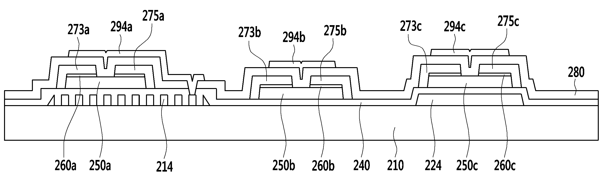
본 발명의 일 실시예에 따른 광 감지 센서는 투명한 유리 또는 플라스틱 재질의 기판(210), 기판(210) 위에 서로 교차하여 형성되는 복수의 게이트선(221)과 데이터선(271), 게이트선(221) 및 데이터선(271)과 연결되는 스위칭 박막 트랜지스터(SW), 스위칭 박막 트랜지스터(SW)와 연결되는 적외선 감지 박막 트랜지스터(IR) 및 가시광선 감지 박막 트랜지스터(VIS)를 포함한다.A photosensitive sensor according to an embodiment of the present invention includes a
게이트선(221)과 데이터선(271)은 복수의 화소를 정의하고, 하나의 화소 내에는 하나의 스위칭 박막 트랜지스터(SW)와 하나의 적외선 감지 박막 트랜지스터(IR)가 서로 연결되어 형성될 수 있고, 인접한 다른 화소 내에는 하나의 스위칭 박막 트랜지스터(SW)와 하나의 가시광선 감지 박막 트랜지스터(VIS)가 서로 연결되어 형성될 수 있다.The
적외선 감지 박막 트랜지스터(IR)는 기판(210) 위에 형성되는 밴드패스필터(214), 밴드패스필터(214) 위에 형성되는 제1 반도체층(250a), 제1 반도체층(250a) 위에 형성되는 제1 저항성 접촉층(260a), 제1 저항성 접촉층(260a) 위에 형성되는 제1 소스 전극(273a) 및 제1 드레인 전극(275a), 제1 소스 전극(273a) 및 제1 드레인 전극(275a) 위에 형성되는 제4 절연막(280), 제4 절연막(280) 위에 형성되는 제1 상부 게이트 전극(294a)을 포함한다.The infrared sensing thin film transistor IR includes a
밴드패스필터(214)는 제1 반도체층(250a)에 가시광선이 입사하는 것을 방지하기 위한 층이다. 제1 반도체층(250a)은 적외선 영역에서 양자 효율이 높지만, 가시광선 영역에서도 양자 효율이 높아 가시광선에도 영향을 받게 되므로, 제1 반도체층(250a)으로 가시광선이 입사하는 것을 방지할 필요가 있다. 밴드패스필터(214)는 금속막에 특정 파장의 빛만이 선택적으로 투과되도록 선형 패턴을 형성하여 빛을 필터링 하도록 하여, 적외선 영역의 파장만이 통과되도록 할 수 있다. The
본 실시예에 따른 밴드패스필터(214)는 금속막에 다수의 구멍(Hole)을 포함하여 형성될 수 있으며, 또는 기판(210)의 위에 막대 또는 바(bar)형상의 금속 입자를 배열함으로써 형성될 수 있다. The
제1 반도체층(250a)은 비정질 실리콘 게르마늄(a-SiGe)으로 형성될 수 있다. 비정질 실리콘 게르마늄(a-SiGe)은 적외선 영역에서 양자 효율이 높은 물질이다. 이때, 제1 반도체층(250a)은 비정질 실리콘 게르마늄(a-SiGe) 대신 다른 물질로 형성될 수도 있으며, 적외선 영역에서 양자 효율이 높은 물질이라면 어느 것도 가능하다.The
제1 소스 전극(273a)과 제1 드레인 전극(275a)은 서로 이격되어 형성됨으로써 채널을 형성한다. 제1 저항성 접촉층(260a)은 제1 반도체층(250a) 위에 채널 부분을 제외하고 형성된다.The
또한, 적외선 감지 박막 트랜지스터(IR)는 기판(210) 위에 적층되어 형성되고 밴드패스필터(214) 아래에 위치하는 제1 절연막(도시하지 않음) 및 밴드패스필터(214)의 위에 위치하는 제2 절연막(240)을 더 포함할 수 있다.In addition, the infrared sensing thin film transistor (IR) is formed by being stacked on the
제1 절연막(도시하지 않음)은 실리콘 질화물(SiNx)로 형성될 수 있으며, 기판(210)과 밴드패스필터(214) 사이의 접착력을 향상시키기 위한 층이다. The first insulating layer (not shown) may be formed of silicon nitride (SiNx) and is a layer for improving adhesion between the
제2 절연막(240)은 실리콘 질화물(SiNx)로 형성될 수 있으며, 밴드패스필터(214)와 제1 반도체층(250a) 사이에 형성되어 계면 특성을 향상하는 역할을 할 수 있다.The second
가시광선 감지 박막 트랜지스터(VIS)는 기판(210) 위에 형성되는 제2 반도체층(250b), 제2 반도체층(250b) 위에 형성되는 제2 저항성 접촉층(260b), 제2 저항성 접촉층(260b) 위에 형성되는 제2 소스 전극(273b) 및 제2 드레인 전극(275b), 제2 소스 전극(273b) 및 제2 드레인 전극(275b) 위에 형성되는 제4 절연막(280), 제4 절연막(280) 위에 형성되는 제2 하부 게이트 전극(294b)을 포함한다.The visible light sensing thin film transistor VIS includes a
제2 반도체층(250b)은 비정질 실리콘(a-Si)으로 형성될 수 있다. 비정질 실리콘(a-Si)은 가시광선 영역에서 양자 효율(quantum efficiency)이 높은 물질로써, 적외선 영역의 빛이 함께 입사되더라도 가시광선 영역의 감도가 높은 특성이 있다. 이때, 제2 반도체층(250b)은 비정질 실리콘(a-Si) 대신 다른 물질로 형성될 수도 있으며, 가시광선 영역에서 양자 효율이 높은 물질이라면 어느 것이라도 가능하다.The
제2 소스 전극(273b)과 제2 드레인 전극(275b)은 서로 이격되어 형성됨으로써 채널을 형성한다. 제2 저항성 접촉층(260b)은 제2 반도체층(250b) 위에 채널 부분을 제외하고 형성된다. The
스위칭 박막 트랜지스터(SW)는 기판(210) 위에 형성되는 제3 반도체층(250c), 제3 반도체층(250c) 위에 형성되는 제3 저항성 접촉층(260c), 제3 저항성 접촉층(260c) 위에 형성되는 제3 소스 전극(273c) 및 제3 드레인 전극(275c), 제3 소스 전극(273c) 및 제3 드레인 전극(275c) 위에 형성되는 제4 절연막(280), 제4 절연막(280) 위에 형성되는 제3 상부 게이트 전극(294c)을 포함한다.The switching thin film transistor SW is formed on the
제3 반도체층(250c)은 비정질 실리콘(a-Si)으로 형성될 수 있다.The
제3 소스 전극(273c)과 제3 드레인 전극(275c)은 서로 이격되어 형성됨으로써 채널을 형성한다. 제3 저항성 접촉층(260c)은 제3 반도체층(250c) 위에 채널 부분을 제외하고 형성된다. The
제3 소스 전극(273c)은 데이터선(271)과 연결되어 데이터선(271)으로부터 데이터 전압을 인가받는다.The
스위칭 박막 트랜지스터(SW)가 적외선 감지 박막 트랜지스터(IR)와 연결되는 화소 내에서는 제3 드레인 전극(275c)이 제1 소스 전극(273a)과 연결된다. 스위칭 박막 트랜지스터(SW)가 가시광선 감지 박막 트랜지스터(VIS)와 연결되는 화소 내에서는 제3 드레인 전극(275c)이 제2 소스 전극(273b)과 연결된다.In the pixel in which the switching thin film transistor SW is connected to the infrared sensing thin film transistor IR, the
스위칭 박막 트랜지스터(SW)는 기판(210) 위에 형성되고 제3 반도체층(250c) 아래에 위치하는 하부 게이트 전극(294), 하부 게이트 전극(294) 위에 형성되는 제2 절연막(240)을 더 포함할 수 있다.The switching thin film transistor SW further includes a lower gate electrode 294 formed on the
제2 절연막(240) 및 제4 절연막(280)에는 하부 게이트 전극(224)을 노출시키도록 접촉 구멍이 형성될 수 있다. 이때 접촉 구멍을 통해 제3 상부 게이트 전극(294c)은 하부 게이트 전극(224)과 연결된다.Contact holes may be formed in the second insulating
그러면 앞에서 설명한 도면들과 함께, 도 3 내지 도 9를 참고하여 본 발명의 실시예에 따른 광 감지 센서의 밴드패스필터(214)에 대하여 설명하도록 한다. 본 발명에 따르면 밴드패스필터(214)는 금속막에 특정 파장의 빛만이 선택적으로 투과되도록 선형 패턴을 형성함으로써 빛을 필터링 하는 표면 플라즈몬 현상을 이용할 수 있다.Next, the
표면 플라즈몬 현상이란 나노 수준의 주기적인 패턴을 갖는 금속 표면에 빛이 입사할 경우 특정 파장의 빛과 금속 표면의 자유전자가 공명을 일으켜 특정 파장의 빛을 형성하는 현상을 말한다. 입사된 빛에 의해 표면 플라즈몬을 형성할 수 있는 특정 파장의 빛만이 홀을 투과할 수 있으며 나머지 빛은 모두 금속 표면에 의해 반사가 이루어진다.The surface plasmon phenomenon refers to a phenomenon in which light of a specific wavelength and free electrons on the metal surface resonate to form light of a specific wavelength when light is incident on a metal surface having a nano-level periodic pattern. Only light of a specific wavelength that can form surface plasmons by the incident light can pass through the hole, and all other light is reflected by the metal surface.
이와 같은 특성을 이용하여 선형 패턴의 주기를 조절하여 원하는 빛만을 투과시킴으로써, 적외선 영역의 빛을 분리할 수 있다. By controlling the period of the linear pattern using such a characteristic to transmit only desired light, light in the infrared region can be separated.
도 3은 본 발명의 일 실시예에 따른 광 감지 센서의 밴드패스필터(214)를 나타낸 도면이다. 본 실시예에 따른 밴드패스필터(214)는 금속막에 다수의 구멍(Hole)을 포함하여 형성될 수 있다. 금속막은 알루미늄, 몰리브덴, 구리, 금, 은, 크롬 등일 수 있으나, 본 발명은 반드시 이에 한하는 것은 아니다. 3 is a diagram illustrating a
이때 투과되는 빛의 파장은 선형 패턴 간격의 약 1.7~2배에 해당하는 파장을 갖게 된다. 따라서 본 실시예에 따른 광 감지 센서는 가시광선 영역의 빛을 반사시키고, 780nm의 적외선 영역의 빛을 통과시키기 위하여 구멍 간의 간격을 390nm 내지 460nm가 되도록 형성 할 수 있다. At this time, the wavelength of the transmitted light has a wavelength corresponding to about 1.7 to 2 times the linear pattern interval. Therefore, the photodetector according to the present embodiment may be formed such that the distance between the holes is 390 nm to 460 nm in order to reflect light in the visible ray region and transmit light in the infrared region of 780 nm.
아울러 금속막에 형성된 다수의 구멍의 형태는 도 4 내지 도 6에 도시된 바와 같이 사각형, 다각형, 슬릿 등의 다양한 형태로 변경할 수도 있다.In addition, the shape of the plurality of holes formed in the metal film may be changed to various shapes such as a rectangle, a polygon, and a slit as shown in FIGS. 4 to 6 .
도 7은 본 발명의 다른 실시예에 따른 광 감지 센서의 밴드패스필터를 나타낸 도면이다. 본 실시예에 따른 밴드패스필터(214)는 기판(210)의 위에 막대 또는 바(bar)형상의 금속입자를 배열함으로써 형성될 수 있다. 금속입자는 알루미늄, 몰리브덴, 구리, 금, 은, 크롬 등일 수 있으나, 본 발명은 반드시 이에 한하는 것은 아니다. 한편 금속입자는 도 7에 도시된 바와 같이 정사각형일 수 있고, 도 8 내지 도 9에 도시된 바와 같이, 원형이거나 직사각형 등의 다양한 형태로 변경할 수 있다.7 is a diagram illustrating a band pass filter of a light detection sensor according to another embodiment of the present invention. The
이때 투과되는 빛의 파장은 선형 패턴 간격의 약 1.7~2배에 해당하는 파장을 갖게 된다. 따라서 본 실시예에 따른 광 감지 센서는 가시광선 영역의 빛을 반사시키고, 780nm의 적외선 영역의 빛을 통과시키기 위하여 금속입자 간의 간격을 390nm 내지 460nm가 되도록 형성 할 수 있다. At this time, the wavelength of the transmitted light has a wavelength corresponding to about 1.7 to 2 times the linear pattern interval. Therefore, the light sensor according to the present embodiment can be formed such that the distance between the metal particles is 390 nm to 460 nm in order to reflect light in the visible ray region and transmit light in the infrared region of 780 nm.
이로 인하여, 적외선 감지 박막 트랜지스터 반도체 층 아래에 밴드패스필터를 형성함으로써, 가시광선이 입사하는 것을 방지하고, 이로 인하여 센서의 오동작을 방지할 수 있다.For this reason, by forming a bandpass filter under the infrared sensing thin film transistor semiconductor layer, it is possible to prevent incident of visible light, thereby preventing malfunction of the sensor.
또한 본 실시예에 의한 광 감지 센서는 금속막에 형성된 다수의 구멍을 포함하는 밴드패스필터를 형성하고, 구멍 간의 간격과 구멍의 형태를 제어함으로써 원하는 파장의 영역을 통과시킨다는 점에서 단순한 재료의 물성을 이용하는 필터보다 정확한 필터링 기능을 수행할 수 있다. In addition, the optical sensor according to the present embodiment forms a band-pass filter including a plurality of holes formed in a metal film, and controls the distance between the holes and the shape of the holes to pass the region of a desired wavelength. It is possible to perform a more accurate filtering function than a filter using
이어, 첨부된 도면을 참조하여 본 발명의 일실시예에 따른 광 감지 센서의 제조 방법에 대해 설명하면 다음과 같다.Next, a method of manufacturing a photosensitive sensor according to an embodiment of the present invention will be described with reference to the accompanying drawings.
도 10a 내지 도 10f 본 발명의 하나의 실시예에 의한 광 감지 센서의 제조 방법을 나타낸 공정 단면도이다.10A to 10F are cross-sectional views illustrating a method of manufacturing a photosensitive sensor according to an embodiment of the present invention.
먼저 도 10a에 도시된 바와 같이 투명한 유리 또는 플라스틱 따위로 만들어진 기판(210) 위에 제1 절연막(도시하지 않음), 밴드패스필터(214) 및 하부 게이트 전극(224)을 형성한다.First, as shown in FIG. 10A , a first insulating layer (not shown), a
제1 절연막(도시하지 않음)은 리튬 플로라이드(LiF) 또는 실리콘 질화물(SiNx) 등으로 형성할 수 있으며, 기판(210)과 밴드패스필터(214) 사이의 접착력을 향상시키기 위한 층이다.The first insulating layer (not shown) may be formed of lithium fluoride (LiF) or silicon nitride (SiNx), and is a layer for improving adhesion between the
이어, 밴드패스필터(214)와 하부 게이트 전극(224)을 형성한다. Next, the
밴드패스필터(214)는 가시광선이 입사하는 것을 방지하기 위한 층이다. 본 실시예에 따르면, 밴드패스필터(214)는 금속막에 특정 파장의 빛만이 선택적으로 투과되도록 선형 패턴을 형성하여 빛을 필터링 하도록 하여, 적외선 영역의 파장만이 통과되도록 할 수 있다.The
이때 밴드패스필터(214)의 선형 패턴은 금속막에 다수의 홀을 형성하거나, 금속입자를 배열함으로써 형성할 수 있다. 이때 금속막 또는 금속입자는 알루미늄, 몰리브덴, 구리, 금, 은, 크롬 등일 수 있고, 금속막에 형성된 다수의 구멍간의 간격과 금속입자들 간의 간격은 390nm 내지 460nm가 되도록 형성할 수 있다.In this case, the linear pattern of the
한편, 밴드패스필터(214)는 금속막 위에 소정의 감광막을 형성한 후, 포토리소그래피공정을 통해 선택적으로 패터닝 하여 감광막 패턴을 형성한 이후, 감광막 패턴을 마스크로 그 하부의 금속막을 선택적으로 패터닝 함으로써 다수의 구멍을 형성할 수 있다.On the other hand, the band-
또는, 금속막 위에 소정의 레지스트를 형성한 후, 몰드로 이루어진 롤러를 임프린팅하여 소정의 레지스트 패턴을 형성한 이후, 레지스트 패턴을 마스크로 그 하부의 금속층을 선택작으로 패터닝 함으로써 다수의 구멍을 형성할 수도 있다.Alternatively, a predetermined resist is formed on the metal film, and then a predetermined resist pattern is formed by imprinting a roller made of a mold, and then a plurality of holes are formed by selectively patterning the underlying metal layer using the resist pattern as a mask. You may.
하부 게이트 전극(224)은 밴드패스필터(214)와 동일한 전도성 물질로 형성될 수 있고, 동일한 마스크를 이용하여 패터닝 된다. The
즉, 본 실시예에 의한 광 감지 센서는 밴드패스필터와 하부 게이트 전극을 동일 평면 상에 형성하고, 밴드패스필터와 하부 게이트 전극을 동일한 재질로 제조함으로써 제조 공정을 단순화하고, 제조 비용을 저감할 수 있다는 효과가 있다.That is, in the photosensitive sensor according to this embodiment, the bandpass filter and the lower gate electrode are formed on the same plane, and the bandpass filter and the lower gate electrode are made of the same material, thereby simplifying the manufacturing process and reducing the manufacturing cost. It has the effect that it can.
또한 본 실시예에 의한 광 감지 센서는 금속막에 형성된 다수의 구멍을 포함하는 밴드패스필터를 형성하고, 구멍 간의 간격과 구멍의 형태를 제어함으로써 원하는 파장의 영역을 통과시킨다는 점에서 단순히 재료 본연의 물성을 이용한 필터에 비하여 정확한 필터링 기능을 수행할 수 있다. In addition, the photosensitive sensor according to this embodiment forms a band-pass filter including a plurality of holes formed in the metal film, and controls the distance between the holes and the shape of the holes to pass the region of the desired wavelength simply in that the material itself is Compared to a filter using physical properties, it is possible to perform an accurate filtering function.
도 10b에 도시된 바와 같이, 제1 절연막(도시하지 않음), 밴드패스필터(214) 및 하부 게이트 전극(224)을 포함한 기판(210)의 전면에 제2 절연막(240)을 형성하고, 기판(210) 위에 제2 반도체층(250b) 및 제2 저항성 접촉층(260b)을, 하부 게이트 전극(224) 위에 제3 반도체층(250c) 및 제3 저항성 접촉층(260c)을 적층하여 형성한다. As shown in FIG. 10B , a second insulating
제2 반도체층(250b) 및 제3 반도체층(250c)은 동일한 물질로 형성할 수 있고, 예를 들면 비정질 실리콘(a-Si)으로 형성할 수 있다. 비정질 실리콘(a-Si)은 가시광선 영역에서 양자 효율(quantum efficiency)이 높은 물질로써, 적외선 영역의 빛이 함께 입사되더라도 가시광선 영역의 감도가 높은 장점이 있다. 이때, 제2 반도체층(250b) 및 제3 반도체층(250c)은 비정질 실리콘(a-Si) 대신 다른 물질로 형성될 수도 있으며, 가시광선 영역에서 양자 효율이 높은 물질이라면 어느 것이라도 가능하다.The
제2 저항성 접촉층(260b) 및 제3 저항성 접촉층(260c)은 동일한 물질로 형성할 수 있다. The second
도 10c에 도시된 바와 같이, 밴드패스필터(214) 위에 제1 반도체층(250a)과 제1 저항성 접촉층(260a)를 형성한다. 제1 반도체층(250a)은 예를 들면 비정질 실리콘 게르마늄(a-SiGe)으로 형성할 수 있다. 비정질 실리콘 게르마늄(a-SiGe)은 적외선 영역에서 양자 효율이 높은 물질로써 적외선 영역의 감도가 높은 장점이 있다. 이때, 제1 반도체층(250a)는 비정질 실리콘 게르마늄(a-SiGe) 대신 다른 물질로 형성될 수도 있으며, 적외선 영역에서 양자 효율이 높은 물질이라면 어느 것도 가능하다. As shown in FIG. 10C , a
도 10d에 도시된 바와 같이, 제1 저항성 접촉층(260a) 위에 제1 소스 전극(273a) 및 제1 드레인 전극(275a)을, 제2 저항성 접촉층(260b) 위에 제2 소스 전극(273b) 및 제2 드레인 전극(275b)를, 제3 저항성 접촉층(260c) 위에 제3 소스 전극(273c) 및 제3 드레인 전극(275c)를 형성한다.As shown in FIG. 10D , the
제1 소스 전극(273a)과 제1 드레인 전극(275a), 제2 소스 전극(273b)와 제2 드레인 전극(275b), 제3 소스 전극(273c)와 제3 드레인 전극(275c)은 각각 서로 이격되도록 하여 채널을 형성한다. 이때, 채널 부분에 대응하여 형성되어 있는 제1 저항성 접촉층(260a), 제2 저항성 접촉층(260b), 제3 저항성 접촉층(260c)를 제거한다.The
도 10e에 도시된 바와 같이, 제1 소스 전극(273a), 제1 드레인 전극(275a), 제2 소스 전극(273b), 제2 드레인 전극(275b), 제3 소스 전극(273c), 및 제3 드레인 전극(275c)을 포함한 기판(210) 전면에 제4 절연막(280)을 형성한다.As shown in FIG. 10E , a
이어, 밴드패스필터(214)를 노출시키도록 제2 절연막(240) 및 제4 절연막(280)에 접촉 구멍(281)을 형성한다. Next, a contact hole 281 is formed in the second insulating
도 10f에 도시된 바와 같이, 제4 절연막(280) 위에 제1 소스 전극(273a) 및 제1 드레인 전극(275a)에 대응하여 제1 상부 게이트 전극(294a)을, 제2 소스 전극(273b) 및 제2 드레인 전극(275b)에 대응하여 제2 하부 게이트 전극(294b)를, 제3 소스 전극(273c) 및 제3 드레인 전극(275c)에 대응하여 제3 상부 게이트 전극(294c)를 형성한다.As shown in FIG. 10F , a first
제1 상부 게이트 전극(294a)은 접촉 구멍(281)을 통해 밴드패스필터(214)와 연결한다.The first
이상에서 본 발명의 바람직한 실시예에 대하여 상세하게 설명하였지만 본 발명의 권리범위는 이에 한정되는 것은 아니고 다음의 청구범위에서 정의하고 있는 본 발명의 기본 개념을 이용한 당업자의 여러 변형 및 개량 형태 또한 본 발명의 권리범위에 속하는 것이다.Although the preferred embodiment of the present invention has been described in detail above, the scope of the present invention is not limited thereto, and various modifications and improvements by those skilled in the art using the basic concept of the present invention as defined in the following claims are also provided. is within the scope of the
210 : 기판 214 : 밴드패스필터
221 : 게이트선 224 : 하부 게이트 전극
240 : 제2 절연막 242 : 제3 절연막
250a : 제1 반도체층 250b : 제2 반도체층
250c : 제3 반도체층 260a : 제1 저항성 접촉층
260b : 제2 저항성 접촉층 260c : 제3 저항성 접촉층
273a : 제1 소스 전극 273b : 제2 소스 전극
273c : 제3 소스 전극 275a : 제1 드레인 전극
275b : 제2 드레인 전극 275c : 제3 드레인 전극
280 : 제4 절연막 281 : 접촉 구멍
294a : 제1 상부 게이트 전극 294b : 제2 상부 게이트 전극
294c : 제3 상부 게이트 전극 210: substrate 214: band pass filter
221: gate line 224: lower gate electrode
240: second insulating film 242: third insulating film
250a:
250c:
260b: second
273a:
273c:
275b:
280: fourth insulating film 281: contact hole
294a: first
294c: third upper gate electrode
Claims (18)
상기 기판 위에 형성되어 적외선 영역의 빛에 의해 동작하는 제1 반도체층 및 적외선 영역의 빛을 통과시키는 밴드패스필터를 포함하는 적외선 감지 박막 트랜지스터;
상기 기판 위에 형성되어 가시광선 영역의 빛에 의해 동작하는 제2 반도체층을 포함하는 가시광선 감지 박막 트랜지스터; 그리고
상기 기판 위에 형성되는 제3 반도체층 및 상기 제3 반도체층과 중첩하는 하부 게이트 전극을 포함하는 스위칭 박막 트랜지스터
를 포함하며,
상기 밴드패스필터는 금속으로 이루어지고, 일정한 주기를 갖는 선형 패턴이 형성되어 가시광선 영역의 빛을 차단하고,
상기 하부 게이트 전극은 상기 밴드패스필터와 동일한 물질을 포함하고 동일한 층에 형성되고,
상기 적외선 감지 박막 트랜지스터는,
상기 제1 반도체층 위에 형성된 제1 소스 전극 및 제1 드레인 전극;
상기 제1 소스 전극 및 상기 제1 드레인 전극 위에 위치하며 상기 밴드패스필터 위의 접촉 구멍을 포함하는 제1 절연막; 그리고
상기 제1 절연막 위에 위치하는 제1 상부 게이트 전극
을 포함하고,
상기 제1 상부 게이트 전극은 상기 접촉 구멍을 통해 상기 밴드패스필터와 직접 연결되는
광 감지 센서.Board;
an infrared sensing thin film transistor formed on the substrate and including a first semiconductor layer operated by infrared light and a bandpass filter passing infrared light;
a visible ray sensing thin film transistor formed on the substrate and including a second semiconductor layer operated by light in a visible ray region; and
A switching thin film transistor including a third semiconductor layer formed on the substrate and a lower gate electrode overlapping the third semiconductor layer
includes,
The band-pass filter is made of metal, and a linear pattern having a certain period is formed to block light in the visible ray region,
The lower gate electrode includes the same material as the band pass filter and is formed on the same layer,
The infrared sensing thin film transistor,
a first source electrode and a first drain electrode formed on the first semiconductor layer;
a first insulating layer disposed on the first source electrode and the first drain electrode and including a contact hole on the band pass filter; and
a first upper gate electrode positioned on the first insulating layer
including,
The first upper gate electrode is directly connected to the band pass filter through the contact hole.
light sensor.
상기 밴드패스필터는 금속막에 다수의 구멍을 포함하여 형성되는 광 감지 센서. In claim 1,
The band-pass filter is a photosensitive sensor formed by including a plurality of holes in the metal film.
상기 금속막은 알루미늄, 몰리브덴, 구리, 금, 은, 크롬 등으로 이루어 지고,
상기 구멍의 형태는 원형, 사각형, 다각형, 슬릿형 중 어느 하나 이상을 포함하고 다수의 구멍 간의 간격은 390nm 내지 460nm 가 되도록 형성된 광 감지 센서.In claim 2,
The metal film is made of aluminum, molybdenum, copper, gold, silver, chromium, etc.,
The shape of the hole includes any one or more of a circle, a rectangle, a polygon, and a slit, and an interval between the plurality of holes is formed to be 390 nm to 460 nm.
상기 밴드패스필터는 상기 기판 위에 금속입자를 배열하여 형성되는 광 감지 센서.In claim 1,
The band pass filter is an optical sensor formed by arranging metal particles on the substrate.
상기 금속입자는 알루미늄, 몰리브덴, 구리, 금, 은, 크롬 등으로 이루어 지고,
상기 금속입자의 형태는 원형, 정사각형, 직사각형 중 어느 하나 이상을 포함하고 상기 금속입자 간의 간격은 390nm 내지 460nm가 되도록 형성된 광 감지 센서.In claim 4,
The metal particles are made of aluminum, molybdenum, copper, gold, silver, chromium, etc.,
The shape of the metal particles includes at least one of a circle, a square, and a rectangle, and the distance between the metal particles is formed to be 390 nm to 460 nm.
상기 제1 반도체층은 비정질 실리콘 게르마늄을 포함하는 광 감지 센서. In claim 1,
The first semiconductor layer is a photosensitive sensor including amorphous silicon germanium.
상기 적외선 감지 박막 트랜지스터는,
상기 제1 반도체층 위에 형성되는 제1 저항성 접촉층을 더 포함하는 광 감지 센서.In claim 1,
The infrared sensing thin film transistor,
The photosensitive sensor further comprising a first ohmic contact layer formed on the first semiconductor layer.
상기 제2 반도체층 및 상기 제3 반도체층은 비정질 실리콘을 포함하는 광 감지 센서.In claim 1,
and the second semiconductor layer and the third semiconductor layer include amorphous silicon.
상기 가시광선 감지 박막 트랜지스터는,
상기 제2 반도체층 위에 형성되는 제2 저항성 접촉층;
상기 제2 저항성 접촉층 위에 형성되는 제2 소스 전극 및 제2 드레인 전극;
상기 제2 소스 전극 및 상기 제2 드레인 전극 위에 형성되는 제2 절연막; 및,
상기 제2 절연막 위에 형성되는 제2 상부 게이트 전극을 더 포함하는,
광 감지 센서.In claim 1,
The visible light sensing thin film transistor,
a second ohmic contact layer formed on the second semiconductor layer;
a second source electrode and a second drain electrode formed on the second ohmic contact layer;
a second insulating layer formed on the second source electrode and the second drain electrode; and,
Further comprising a second upper gate electrode formed on the second insulating film,
light sensor.
상기 스위칭 박막 트랜지스터는,
상기 하부 게이트 전극 위에 형성되는 제3 절연막;
상기 제3 반도체층 위에 형성되는 제3 저항성 접촉층;
상기 제3 저항성 접촉층 위에 형성되는 제3 소스 전극 및 제3 드레인 전극;
상기 제3 소스 전극 및 상기 제3 드레인 전극 위에 형성되는 상기 제1 절연막; 및,
상기 제1 절연막 위에 형성되는 제3 상부 게이트 전극을 더 포함하는,
광 감지 센서.In claim 1,
The switching thin film transistor,
a third insulating layer formed on the lower gate electrode;
a third ohmic contact layer formed on the third semiconductor layer;
a third source electrode and a third drain electrode formed on the third ohmic contact layer;
the first insulating layer formed on the third source electrode and the third drain electrode; and,
Further comprising a third upper gate electrode formed on the first insulating film,
light sensor.
Priority Applications (3)
| Application Number | Priority Date | Filing Date | Title |
|---|---|---|---|
| KR1020150050426A KR102297206B1 (en) | 2015-04-09 | 2015-04-09 | Optical sensor and method for manufacturing the same |
| US15/061,852 US10079326B2 (en) | 2015-04-09 | 2016-03-04 | Optical sensor and method of manufacture |
| CN201610217594.0A CN106057841B (en) | 2015-04-09 | 2016-04-08 | Optical sensor and method of making the same |
Applications Claiming Priority (1)
| Application Number | Priority Date | Filing Date | Title |
|---|---|---|---|
| KR1020150050426A KR102297206B1 (en) | 2015-04-09 | 2015-04-09 | Optical sensor and method for manufacturing the same |
Publications (2)
| Publication Number | Publication Date |
|---|---|
| KR20160121671A KR20160121671A (en) | 2016-10-20 |
| KR102297206B1 true KR102297206B1 (en) | 2021-09-02 |
Family
ID=57112842
Family Applications (1)
| Application Number | Title | Priority Date | Filing Date |
|---|---|---|---|
| KR1020150050426A Active KR102297206B1 (en) | 2015-04-09 | 2015-04-09 | Optical sensor and method for manufacturing the same |
Country Status (3)
| Country | Link |
|---|---|
| US (1) | US10079326B2 (en) |
| KR (1) | KR102297206B1 (en) |
| CN (1) | CN106057841B (en) |
Families Citing this family (7)
| Publication number | Priority date | Publication date | Assignee | Title |
|---|---|---|---|---|
| KR102801934B1 (en) | 2016-12-05 | 2025-05-07 | 삼성디스플레이 주식회사 | Display device |
| KR102636068B1 (en) * | 2016-12-28 | 2024-02-14 | 삼성디스플레이 주식회사 | Scan driver and display device having the same |
| KR102454368B1 (en) * | 2018-01-22 | 2022-10-14 | 삼성전자주식회사 | Memory package and semiconductor package |
| CN108388056B (en) * | 2018-03-15 | 2021-08-06 | 京东方科技集团股份有限公司 | Display panel and method of making the same |
| KR102572431B1 (en) * | 2018-08-22 | 2023-08-29 | 엘지디스플레이 주식회사 | Display device |
| JP7615703B2 (en) * | 2021-01-21 | 2025-01-17 | 富士通株式会社 | Graphene Optical Sensor |
| CN115704715A (en) * | 2021-08-06 | 2023-02-17 | 财团法人工业技术研究院 | MEMS infrared light sensing device and manufacturing method thereof |
Citations (1)
| Publication number | Priority date | Publication date | Assignee | Title |
|---|---|---|---|---|
| US20150002843A1 (en) * | 2013-06-28 | 2015-01-01 | Sony Corporation | Image capture device and electronic apparatus |
Family Cites Families (14)
| Publication number | Priority date | Publication date | Assignee | Title |
|---|---|---|---|---|
| KR101264728B1 (en) | 2009-10-23 | 2013-05-15 | 엘지디스플레이 주식회사 | Liquid Crystal Display Device |
| KR101669964B1 (en) | 2010-02-02 | 2016-10-28 | 삼성디스플레이 주식회사 | Touch screen substrate and method of manufacturing the same |
| KR101343293B1 (en) * | 2010-04-30 | 2013-12-18 | 샤프 가부시키가이샤 | Circuit board and display device |
| KR101699399B1 (en) | 2010-08-12 | 2017-01-25 | 삼성디스플레이 주식회사 | Visible sensing transistor, display panel and manufacturing method thereof |
| CN101963716B (en) * | 2010-09-10 | 2013-09-25 | 钰瀚科技股份有限公司 | LCD Monitor |
| KR20120060407A (en) | 2010-12-02 | 2012-06-12 | 삼성전자주식회사 | Display substrate, method of manufacturing the same and touch display apparatus having the display substrate |
| KR101743268B1 (en) | 2010-12-06 | 2017-06-05 | 삼성디스플레이 주식회사 | Light sensor and display apparatus having the same |
| KR101770969B1 (en) | 2011-01-21 | 2017-08-25 | 삼성디스플레이 주식회사 | Substrate of sensing touch and method of manufacturing the substrate |
| KR101829777B1 (en) | 2011-03-09 | 2018-02-20 | 삼성디스플레이 주식회사 | Optical sensor |
| KR20120111637A (en) | 2011-04-01 | 2012-10-10 | 삼성디스플레이 주식회사 | Optical sensor |
| EP2699990A4 (en) | 2011-04-19 | 2015-01-21 | Perceptive Pixel Inc | Optical filtered sensor-in-pixel technology for touch sensing |
| US8749529B2 (en) | 2012-03-01 | 2014-06-10 | Microsoft Corporation | Sensor-in-pixel display system with near infrared filter |
| KR102068275B1 (en) * | 2012-12-20 | 2020-01-21 | 삼성디스플레이 주식회사 | Thin film transistor array panel and manufacturing method thereof |
| KR102221842B1 (en) | 2014-04-08 | 2021-03-03 | 삼성디스플레이 주식회사 | Sensor substrate, method of manufacturing the same and display apparatus having the same |
-
2015
- 2015-04-09 KR KR1020150050426A patent/KR102297206B1/en active Active
-
2016
- 2016-03-04 US US15/061,852 patent/US10079326B2/en active Active
- 2016-04-08 CN CN201610217594.0A patent/CN106057841B/en active Active
Patent Citations (1)
| Publication number | Priority date | Publication date | Assignee | Title |
|---|---|---|---|---|
| US20150002843A1 (en) * | 2013-06-28 | 2015-01-01 | Sony Corporation | Image capture device and electronic apparatus |
Also Published As
| Publication number | Publication date |
|---|---|
| KR20160121671A (en) | 2016-10-20 |
| US20160300974A1 (en) | 2016-10-13 |
| US10079326B2 (en) | 2018-09-18 |
| CN106057841B (en) | 2021-05-04 |
| CN106057841A (en) | 2016-10-26 |
Similar Documents
| Publication | Publication Date | Title |
|---|---|---|
| KR102297206B1 (en) | Optical sensor and method for manufacturing the same | |
| US9001290B2 (en) | Polarizer, display panel having the same and method of manufacturing the same | |
| KR101290709B1 (en) | Touch sensor in-cell type liquid crystal display device and method of fabricating the same | |
| KR101942363B1 (en) | Polarizer, method of manufacturing the polarizer, display panel having the polarizer and display apparatus having the display panel | |
| KR101936773B1 (en) | Method for manufacturing liquid crystal display device | |
| CN106775165B (en) | Embedded touch display panel and electronic device | |
| KR101978190B1 (en) | Polarizer and method of manufacturing the same | |
| TWI389320B (en) | Display device and manufacturing method thereof, and semiconductor device and manufacturing method thereof | |
| US10908453B2 (en) | Display device and manufacturing method thereof | |
| KR102554120B1 (en) | Liquid crystal display | |
| KR20120136695A (en) | Oxide thin film transistor and method of fabricating the same | |
| KR20140056545A (en) | Liquid crystal display and manufacturing method thereof | |
| US10782805B2 (en) | Touch panel, including blanking layer, touch display device including touch panel and method for manufacturing touch panel | |
| KR20110047767A (en) | Color filter and liquid crystal display using surface plasmon | |
| KR20160049348A (en) | Display panel and method of manufacturing the same | |
| KR20170077957A (en) | Liquid crystal display appartus and method of manufacturing the same | |
| KR20120014502A (en) | Liquid crystal display device including an optical sensor, a manufacturing method of the optical sensor, and the optical sensor | |
| JP2017011266A (en) | Mask and display device manufacturing method using the same | |
| KR20160047642A (en) | Method of manufacturing a polarizer and a display panel having the same | |
| US9087750B2 (en) | Touch screen substrate, method of manufacturing the same, and display panel including the touch screen substrate | |
| JP2009087118A (en) | Touch panel, display device with touch panel, and manufacturing method thereof | |
| KR20080001769A (en) | Liquid crystal display and manufacturing method thereof | |
| KR20150051351A (en) | Thin film transistor substrate and Display Device and Method of manufacturing the sames | |
| KR20100062470A (en) | Display substrate, method of manufacturing the same and display panel having the display substrate | |
| KR20160049162A (en) | A method of manufacturing a mold and a method of manufacturing a polarizer |
Legal Events
| Date | Code | Title | Description |
|---|---|---|---|
| PA0109 | Patent application |
Patent event code: PA01091R01D Comment text: Patent Application Patent event date: 20150409 |
|
| PG1501 | Laying open of application | ||
| A201 | Request for examination | ||
| PA0201 | Request for examination |
Patent event code: PA02012R01D Patent event date: 20200324 Comment text: Request for Examination of Application Patent event code: PA02011R01I Patent event date: 20150409 Comment text: Patent Application |
|
| E902 | Notification of reason for refusal | ||
| PE0902 | Notice of grounds for rejection |
Comment text: Notification of reason for refusal Patent event date: 20210419 Patent event code: PE09021S01D |
|
| E701 | Decision to grant or registration of patent right | ||
| PE0701 | Decision of registration |
Patent event code: PE07011S01D Comment text: Decision to Grant Registration Patent event date: 20210625 |
|
| GRNT | Written decision to grant | ||
| PR0701 | Registration of establishment |
Comment text: Registration of Establishment Patent event date: 20210827 Patent event code: PR07011E01D |
|
| PR1002 | Payment of registration fee |
Payment date: 20210827 End annual number: 3 Start annual number: 1 |
|
| PG1601 | Publication of registration | ||
| PR1001 | Payment of annual fee |
Payment date: 20240723 Start annual number: 4 End annual number: 4 |