KR102288539B1 - Semiconductor device - Google Patents
Semiconductor device Download PDFInfo
- Publication number
- KR102288539B1 KR102288539B1 KR1020150002517A KR20150002517A KR102288539B1 KR 102288539 B1 KR102288539 B1 KR 102288539B1 KR 1020150002517 A KR1020150002517 A KR 1020150002517A KR 20150002517 A KR20150002517 A KR 20150002517A KR 102288539 B1 KR102288539 B1 KR 102288539B1
- Authority
- KR
- South Korea
- Prior art keywords
- memory
- information
- specific information
- code
- emrs
- Prior art date
- Legal status (The legal status is an assumption and is not a legal conclusion. Google has not performed a legal analysis and makes no representation as to the accuracy of the status listed.)
- Active
Links
Images


Classifications
-
- G—PHYSICS
- G06—COMPUTING OR CALCULATING; COUNTING
- G06F—ELECTRIC DIGITAL DATA PROCESSING
- G06F13/00—Interconnection of, or transfer of information or other signals between, memories, input/output devices or central processing units
- G06F13/14—Handling requests for interconnection or transfer
- G06F13/16—Handling requests for interconnection or transfer for access to memory bus
- G06F13/1668—Details of memory controller
- G06F13/1673—Details of memory controller using buffers
-
- G—PHYSICS
- G06—COMPUTING OR CALCULATING; COUNTING
- G06F—ELECTRIC DIGITAL DATA PROCESSING
- G06F12/00—Accessing, addressing or allocating within memory systems or architectures
- G06F12/02—Addressing or allocation; Relocation
- G06F12/08—Addressing or allocation; Relocation in hierarchically structured memory systems, e.g. virtual memory systems
- G06F12/0802—Addressing of a memory level in which the access to the desired data or data block requires associative addressing means, e.g. caches
-
- G—PHYSICS
- G06—COMPUTING OR CALCULATING; COUNTING
- G06F—ELECTRIC DIGITAL DATA PROCESSING
- G06F13/00—Interconnection of, or transfer of information or other signals between, memories, input/output devices or central processing units
- G06F13/14—Handling requests for interconnection or transfer
- G06F13/16—Handling requests for interconnection or transfer for access to memory bus
- G06F13/1668—Details of memory controller
- G06F13/1694—Configuration of memory controller to different memory types
-
- G—PHYSICS
- G11—INFORMATION STORAGE
- G11C—STATIC STORES
- G11C7/00—Arrangements for writing information into, or reading information out from, a digital store
- G11C7/10—Input/output [I/O] data interface arrangements, e.g. I/O data control circuits, I/O data buffers
- G11C7/1078—Data input circuits, e.g. write amplifiers, data input buffers, data input registers, data input level conversion circuits
- G11C7/1084—Data input buffers, e.g. comprising level conversion circuits, circuits for adapting load
-
- G—PHYSICS
- G11—INFORMATION STORAGE
- G11C—STATIC STORES
- G11C8/00—Arrangements for selecting an address in a digital store
- G11C8/10—Decoders
Landscapes
- Engineering & Computer Science (AREA)
- Theoretical Computer Science (AREA)
- Physics & Mathematics (AREA)
- General Engineering & Computer Science (AREA)
- General Physics & Mathematics (AREA)
- Microelectronics & Electronic Packaging (AREA)
- Human Computer Interaction (AREA)
- Dram (AREA)
- Memory System Of A Hierarchy Structure (AREA)
- Memory System (AREA)
- Semiconductor Integrated Circuits (AREA)
Abstract
반도체 장치가 제공된다. 상기 반도체 장치는, 특정 정보를 포함하는 EMRS(Extended Mode Register Set) 코드를 제공받고, 상기 제공받은 EMRS 코드를 디코드하여 상기 특정 정보를 추출하는 디코더; 상기 추출된 특정 정보를 토대로 제어 신호를 생성하는 주변 영역 제어부; 및 상기 제어 신호에 의해 제어되는 복수개의 버퍼를 포함하는 주변 영역을 포함하되, 상기 특정 정보는 상기 복수개의 버퍼 중 어느 하나로 입력되는 입력 데이터의 기대 대역폭에 관한 정보를 포함한다. A semiconductor device is provided. The semiconductor device may include: a decoder that receives an Extended Mode Register Set (EMRS) code including specific information, and decodes the received EMRS code to extract the specific information; a peripheral area controller for generating a control signal based on the extracted specific information; and a peripheral region including a plurality of buffers controlled by the control signal, wherein the specific information includes information about an expected bandwidth of input data input to one of the plurality of buffers.
Description
본 발명은 반도체 장치에 관한 것이다. The present invention relates to a semiconductor device.
휘발성 메모리 예컨대, (DDR(double data rate)-SDRAM(synchronized dynamic random access memory))의 스피드 빈(speed bin), 즉, 데이터 전송 속도가 지속적으로 증가하면서, 커버해야하는 스피드 범위가 넓어지고 있다. 또한 서버(server)향 DRAM의 경우에 채널(channel)에서의 상황, 예컨대 DPC(DIMM per channel) 등에 대한 효과적인 대응이 필요할 수 있다. 이로 인해, DRAM에서 사용되는 스피드 빈과 채널 상황이 매우 다양하기 때문에 이러한 모든 스피드 빈 및 채널 상황에 최적화되도록 설계하는 것이 점점 더 어려워지고 있다. A speed bin of a volatile memory, for example (double data rate (DDR)-synchronized dynamic random access memory (SDRAM)), that is, as the data transfer rate continues to increase, the speed range to be covered is expanding. In addition, in the case of server-oriented DRAM, it may be necessary to effectively respond to a situation in a channel, for example, a DIMM per channel (DPC). Because of this, since the speed bins and channel conditions used in DRAM are very diverse, it is becoming increasingly difficult to design to optimize for all these speed bins and channel conditions.
이에 따라, 이러한 최적화 문제를 해결할 수 있는 방안의 필요성이 증가하고 있다. Accordingly, the need for a method capable of solving such an optimization problem is increasing.
본 발명이 해결하려는 과제는, EMRS(extended mode register set) 코드를 통해 메모리 외부 환경에 대한 정보, 즉, 스피드 빈 또는 DIMM(dual in-line memory module)과 관련된 정보를 메모리로 제공하여 메모리를 최적화시킬 수 있는 반도체 장치를 제공하는 것이다. The problem to be solved by the present invention is to optimize the memory by providing information about the external environment of the memory, that is, information related to the speed bean or DIMM (dual in-line memory module) to the memory through an extended mode register set (EMRS) code To provide a semiconductor device capable of
본 발명이 해결하려는 과제들은 이상에서 언급한 과제들로 제한되지 않으며, 언급되지 않은 또 다른 과제들은 아래의 기재로부터 당업자에게 명확하게 이해될 수 있을 것이다.The problems to be solved by the present invention are not limited to the above-mentioned problems, and other problems not mentioned will be clearly understood by those skilled in the art from the following description.
상기 과제를 해결하기 위한 본 발명의 반도체 장치의 일 실시예는, 특정 정보를 포함하는 EMRS(Extended Mode Register Set) 코드를 제공받고, 상기 제공받은 EMRS 코드를 디코드하여 상기 특정 정보를 추출하는 디코더; 상기 추출된 특정 정보를 토대로 제어 신호를 생성하는 주변 영역 제어부; 및 상기 제어 신호에 의해 제어되는 복수개의 버퍼를 포함하는 주변 영역을 포함하되, 상기 특정 정보는 상기 복수개의 버퍼 중 어느 하나로 입력되는 입력 데이터의 기대 대역폭에 관한 정보를 포함한다.In one embodiment of the present invention, a semiconductor device for solving the above problems includes: a decoder that receives an EMRS (Extended Mode Register Set) code including specific information, and decodes the provided EMRS code to extract the specific information; a peripheral area controller for generating a control signal based on the extracted specific information; and a peripheral region including a plurality of buffers controlled by the control signal, wherein the specific information includes information about an expected bandwidth of input data input to one of the plurality of buffers.
상기 제어 신호는 상기 복수개의 버퍼 중 상기 입력 데이터의 기대 대역폭에 상응하는 버퍼를 활성화시킬 수 있다.The control signal may activate a buffer corresponding to an expected bandwidth of the input data among the plurality of buffers.
상기 EMRS 코드는 메모리 컨트롤러 또는 프로세서로부터 제공받을 수 있다.The EMRS code may be provided from a memory controller or a processor.
상기 프로세서는 CPU 또는 GPU를 포함할 수 있다.The processor may include a CPU or a GPU.
상기 버퍼는 입력 버퍼 또는 출력 버퍼를 포함할 수 있다.The buffer may include an input buffer or an output buffer.
상기 과제를 해결하기 위한 본 발명의 반도체 장치의 다른 실시예는, 특정 정보를 포함하는 EMRS 코드를 생성하는 EMRS 코드 생성부; 및 상기 EMRS 코드를 메모리에 전송하는 EMRS 코드 전송부를 포함하되, 상기 특정 정보는 상기 메모리의 스피드 빈(speed bin) 정보를 포함한다.Another embodiment of the semiconductor device of the present invention for solving the above problems, the EMRS code generator for generating an EMRS code including specific information; and an EMRS code transmitter configured to transmit the EMRS code to a memory, wherein the specific information includes speed bin information of the memory.
상기 메모리는 DIMM에 포함되고, 상기 DIMM은 복수개이고, 상기 특정 정보는 채널 당 할당되는 상기 DIMM의 개수에 관한 정보, 상기 복수개의 DIMM이 어느 슬롯에 장착되는지에 관한 정보 및 상기 DIMM의 랭크(rank)에 관한 정보 중 적어도 하나를 더 포함할 수 있다.The memory is included in a DIMM, the number of DIMMs is plural, and the specific information includes information on the number of DIMMs allocated per channel, information on which slots the plurality of DIMMs are mounted in, and a rank of the DIMM. ) may further include at least one of information on the
상기 과제를 해결하기 위한 본 발명의 반도체 장치의 또 다른 실시예는, EMRS 코드를 생성하는 컨트롤러; 및 상기 EMRS 코드를 통해 특정 정보를 제공받는 메모리를 포함하는 DIMM을 포함하되, 상기 EMRS 코드는 상기 메모리의 동작 모드를 설정하는 코드이고, 상기 DIMM은 복수개이고, 상기 특정 정보는 상기 메모리의 스피드 빈 정보, 채널 당 할당되는 상기 DIMM의 개수에 관한 정보, 상기 복수개의 DIMM이 어느 슬롯에 장착되는지에 관한 정보 및 상기 DIMM의 랭크에 관한 정보 중 적어도 하나를 포함한다.Another embodiment of the semiconductor device of the present invention for solving the above problems, the controller for generating the EMRS code; and a DIMM including a memory receiving specific information through the EMRS code, wherein the EMRS code is a code for setting an operation mode of the memory, the number of DIMMs is plural, and the specific information is a speed bin of the memory information, information on the number of the DIMMs allocated per channel, information on which slots the plurality of DIMMs are mounted in, and information on the rank of the DIMMs.
상기 메모리는 DRAM을 포함할 수 있다.The memory may include DRAM.
상기 메모리는 복수개의 버퍼를 포함하는 주변 영역을 포함할 수 있다.The memory may include a peripheral area including a plurality of buffers.
상기 메모리는 상기 EMRS 코드를 제공받아 디코드(decode)하여 상기 특정 정보를 추출하고, 상기 복수개의 버퍼 중 상기 추출된 특정 정보에 최적화된 버퍼를 활성화시킬 수 있다.The memory may receive the EMRS code, decode it, extract the specific information, and activate a buffer optimized for the extracted specific information among the plurality of buffers.
상기 과제를 해결하기 위한 본 발명의 반도체 장치의 또 다른 실시예는, EMRS 코드를 생성하는 컨트롤러; 및 상기 EMRS 코드를 제공받는 메모리를 포함하는 DIMM을 포함하되, 상기 메모리는, 상기 EMRS 코드를 제공받고, 상기 제공받은 EMRS 코드를 디코드하여 특정 정보를 추출하는 디코더와, 상기 추출된 특정 정보를 토대로 상기 메모리의 주변 영역을 제어하는 제어 신호를 생성하는 주변 영역 제어부를 포함하되, 상기 EMRS 코드는 상기 메모리의 동작 모드를 설정하는 코드이고, 상기 특정 정보는 상기 메모리의 스피드 빈 정보를 포함한다.Another embodiment of the semiconductor device of the present invention for solving the above problems, the controller for generating the EMRS code; and a DIMM including a memory receiving the EMRS code, wherein the memory includes a decoder receiving the EMRS code and decoding the received EMRS code to extract specific information, and based on the extracted specific information and a peripheral region controller for generating a control signal for controlling the peripheral region of the memory, wherein the EMRS code is a code for setting an operation mode of the memory, and the specific information includes speed bin information of the memory.
상기 메모리의 주변 영역은 복수개의 버퍼를 포함하고, 상기 제어 신호는 상기 복수개의 버퍼 중 상기 추출된 특정 정보에 최적화된 버퍼를 활성화시킬 수 있다.The peripheral area of the memory may include a plurality of buffers, and the control signal may activate a buffer optimized for the extracted specific information among the plurality of buffers.
상기 EMRS 코드와 상기 특정 정보 사이의 관계를 정의하는 테이블을 더 포함할 수 있다.It may further include a table defining a relationship between the EMRS code and the specific information.
상기 테이블은 사용자에 의해 정의될 수 있다.The table can be defined by the user.
상기 디코더는, 상기 제공받은 EMRS 코드를 상기 테이블과 비교하여 상기 EMRS 코드와 매칭되는 특정 정보를 추출할 수 있다.The decoder may extract specific information matching the EMRS code by comparing the provided EMRS code with the table.
상기 DIMM은 복수개이고, 상기 특정 정보는 채널 당 할당되는 상기 DIMM의 개수에 관한 정보, 상기 복수개의 DIMM이 어느 슬롯에 장착되는지에 관한 정보 및 상기 DIMM의 랭크에 관한 정보 중 적어도 하나를 더 포함할 수 있다.The number of DIMMs is plural, and the specific information further includes at least one of information on the number of DIMMs allocated per channel, information on which slots the plurality of DIMMs are mounted in, and information on the rank of the DIMMs. can
상기 테이블은, 상기 EMRS 코드와 상기 메모리의 스피드 빈 정보 사이의 관계를 정의하는 제1 테이블과, 상기 EMRS 코드와 채널 당 할당되는 상기 DIMM의 개수에 관한 정보 사이의 관계를 정의하는 제2 테이블과, 상기 EMRS 코드와 상기 복수개의 DIMM이 어느 슬롯에 장착되는지에 관한 정보 사이의 관계를 정의하는 제3 테이블과, 상기 EMRS 코드와 상기 DIMM의 랭크(rank)에 관한 정보 사이의 관계를 정의하는 제4 테이블을 포함할 수 있다.The table includes a first table defining a relationship between the EMRS code and speed bin information of the memory, and a second table defining a relationship between the EMRS code and information on the number of DIMMs allocated per channel; , a third table defining a relationship between the EMRS code and information on which slots the plurality of DIMMs are mounted, and a third table defining a relationship between the EMRS code and information on the rank of the DIMMs It can contain 4 tables.
상기 컨트롤러는 프로세서 또는 메모리 컨트롤러를 포함할 수 있다.The controller may include a processor or a memory controller.
상기 컨트롤러와 상기 DIMM은 버스를 통해 연결될 수 있다.The controller and the DIMM may be connected through a bus.
상기 과제를 해결하기 위한 본 발명의 반도체 장치의 또 다른 실시예는, 보드(board)에 장착되고, EMRS 코드를 생성하는 컨트롤러; 상기 보드에 장착된 슬롯; 및 상기 슬롯에 장착되고, 상기 컨트롤러와 버스를 통해 연결되는 메모리를 포함하는 DIMM을 포함하되, 상기 메모리는 상기 EMRS 코드를 통해 특정 정보를 제공받고, 상기 EMRS 코드는 상기 메모리의 동작 모드를 설정하는 코드이고, 상기 특정 정보는 상기 메모리의 스피드 빈(speed bin) 정보를 포함한다.Another embodiment of the semiconductor device of the present invention for solving the above problems is mounted on a board (board), the controller for generating the EMRS code; a slot mounted on the board; and a DIMM mounted in the slot and including a memory connected to the controller through a bus, wherein the memory is provided with specific information through the EMRS code, and the EMRS code sets an operation mode of the memory code, and the specific information includes speed bin information of the memory.
상기 슬롯 및 상기 DIMM은 각각 복수개이고, 상기 특정 정보는, 채널 당 할당되는 상기 복수개의 DIMM의 개수에 관한 정보, 상기 복수개의 DIMM이 상기 복수개의 슬롯 중 어느 슬롯에 장착되는지에 관한 정보 및 상기 DIMM의 랭크에 관한 정보 중 적어도 하나를 더 포함할 수 있다.The slot and the DIMM are each in plurality, and the specific information includes information on the number of the plurality of DIMMs allocated per channel, information on which slot among the plurality of slots the plurality of DIMMs are mounted in, and the DIMM It may further include at least one of information about the rank of .
상기 채널은 상기 버스와 상기 메모리 사이를 연결할 수 있다.The channel may connect between the bus and the memory.
상기 컨트롤러는 프로세서 또는 메모리 컨트롤러를 포함할 수 있다.The controller may include a processor or a memory controller.
상기 메모리는 복수개이고, 상기 복수개의 메모리는 DRAM일 수 있다.The plurality of memories may be DRAM.
상기 메모리는 복수개의 버퍼를 포함하는 주변 영역을 포함할 수 있다.The memory may include a peripheral area including a plurality of buffers.
상기 메모리는 상기 EMRS 코드를 제공받아 디코드(decode)하여 상기 특정 정보를 추출하고, 상기 복수개의 버퍼 중 상기 추출된 특정 정보에 상응하는 버퍼를 활성화시킬 수 있다.The memory may receive the EMRS code, decode it, extract the specific information, and activate a buffer corresponding to the extracted specific information among the plurality of buffers.
상기 메모리는 코어 영역을 포함하고, 상기 메모리는 상기 EMRS 코드를 제공받아 디코드(decode)하여 상기 특정 정보를 추출하고, 상기 추출된 특정 정보를 이용하여 상기 코어 영역을 제어할 수 있다.The memory may include a core region, and the memory may receive and decode the EMRS code to extract the specific information, and control the core region using the extracted specific information.
상기 과제를 해결하기 위한 본 발명의 반도체 장치의 또 다른 실시예는, 컨트롤러; 및 상기 컨트롤러와 채널을 통해 연결되고, 복수개의 버퍼를 포함하는 메모리를 포함하되, 상기 컨트롤러는 상기 채널의 대역폭 및 상기 복수개의 버퍼 중 어느 하나로 입력되는 입력 데이터의 기대 대역폭에 관한 정보를 EMRS 코드를 통해 상기 메모리에 제공하고, 상기 메모리는 상기 복수개의 버퍼 중 상기 채널의 대역폭 및 상기 입력 데이터의 기대 대역폭에 관한 정보에 최적화된 버퍼를 활성화시킬 수 있다.Another embodiment of the semiconductor device of the present invention for solving the above problems, the controller; and a memory connected to the controller through a channel and including a plurality of buffers, wherein the controller transmits information about the bandwidth of the channel and the expected bandwidth of input data input to any one of the plurality of buffers using an EMRS code. through the memory, and the memory may activate a buffer optimized for information about the bandwidth of the channel and the expected bandwidth of the input data among the plurality of buffers.
상기 복수의 버퍼는 상기 메모리의 주변 영역에 포함될 수 있다.The plurality of buffers may be included in a peripheral area of the memory.
본 발명의 기타 구체적인 사항들은 상세한 설명 및 도면들에 포함되어 있다.Other specific details of the invention are included in the detailed description and drawings.
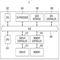
도 1은 본 발명의 일 실시예에 따른 반도체 장치를 설명하는 개략도이다.
도 2는 도 1의 컨트롤러를 설명하는 개략도이다.
도 3은 도 1의 메모리를 설명하는 개략도이다.
도 4는 도 3의 주변 영역을 설명하는 개략도이다.
도 5 및 도 6은 도 3의 디코더에 포함된 테이블을 설명하는 도면들이다.
도 7 및 도 8은 도 1의 컨트롤러, 채널, 메모리 사이의 주파수 영역 관계를 설명하는 도면이다.
도 9는 본 발명의 다른 실시예에 따른 반도체 장치를 설명하는 개략도이다.
도 10은 본 발명의 또 다른 실시예에 따른 반도체 장치를 설명하는 블록도이다.
도 11은 본 발명의 또 다른 실시예에 따른 반도체 장치를 설명하는 블록도이다.
도 12 내지 도 14는 본 발명의 몇몇 실시예들에 따른 반도체 장치를 적용할 수 있는 예시적인 반도체 시스템이다.
도 15는 도 1의 반도체 장치의 동작 방법을 설명하는 순서도이다.1 is a schematic diagram illustrating a semiconductor device according to an embodiment of the present invention.
FIG. 2 is a schematic diagram illustrating the controller of FIG. 1 .
3 is a schematic diagram illustrating the memory of FIG. 1 ;
FIG. 4 is a schematic diagram illustrating the peripheral area of FIG. 3 .
5 and 6 are diagrams for explaining a table included in the decoder of FIG. 3 .
7 and 8 are diagrams for explaining the frequency domain relationship between the controller, the channel, and the memory of FIG. 1 .
9 is a schematic diagram illustrating a semiconductor device according to another embodiment of the present invention.
10 is a block diagram illustrating a semiconductor device according to another embodiment of the present invention.
11 is a block diagram illustrating a semiconductor device according to another embodiment of the present invention.
12 to 14 are exemplary semiconductor systems to which semiconductor devices according to some embodiments of the present invention may be applied.
15 is a flowchart illustrating an operation method of the semiconductor device of FIG. 1 .
본 발명의 이점 및 특징, 그리고 그것들을 달성하는 방법은 첨부되는 도면과 함께 상세하게 후술되어 있는 실시예들을 참조하면 명확해질 것이다. 그러나 본 발명은 이하에서 개시되는 실시예들에 한정되는 것이 아니라 서로 다른 다양한 형태로 구현될 것이며, 단지 본 실시예들은 본 발명의 개시가 완전하도록 하며, 본 발명이 속하는 기술분야에서 통상의 지식을 가진 자에게 발명의 범주를 완전하게 알려주기 위해 제공되는 것이며, 본 발명은 청구항의 범주에 의해 정의될 뿐이다. 도면에서 표시된 구성요소의 크기 및 상대적인 크기는 설명의 명료성을 위해 과장된 것일 수 있다. 명세서 전체에 걸쳐 동일 참조 부호는 동일 구성 요소를 지칭하며, "및/또는"은 언급된 아이템들의 각각 및 하나 이상의 모든 조합을 포함한다.Advantages and features of the present invention and methods of achieving them will become apparent with reference to the embodiments described below in detail in conjunction with the accompanying drawings. However, the present invention is not limited to the embodiments disclosed below, but will be implemented in a variety of different forms, and only these embodiments allow the disclosure of the present invention to be complete, and common knowledge in the technical field to which the present invention belongs It is provided to fully inform the possessor of the scope of the invention, and the present invention is only defined by the scope of the claims. Sizes and relative sizes of components indicated in the drawings may be exaggerated for clarity of description. Like reference numerals refer to like elements throughout, and "and/or" includes each and every combination of one or more of the recited items.
소자(elements) 또는 층이 다른 소자 또는 층의 "위(on)" 또는 "상(on)"으로 지칭되는 것은 다른 소자 또는 층의 바로 위뿐만 아니라 중간에 다른 층 또는 다른 소자를 개재한 경우를 모두 포함한다. 반면, 소자가 "직접 위(directly on)" 또는 "바로 위"로 지칭되는 것은 중간에 다른 소자 또는 층을 개재하지 않은 것을 나타낸다.Reference to an element or layer “on” or “on” another element or layer includes not only directly on the other element or layer, but also with intervening other layers or elements. include all On the other hand, reference to an element "directly on" or "immediately on" indicates that no intervening element or layer is interposed.
공간적으로 상대적인 용어인 "아래(below)", "아래(beneath)", "하부(lower)", "위(above)", "상부(upper)" 등은 도면에 도시되어 있는 바와 같이 하나의 소자 또는 구성 요소들과 다른 소자 또는 구성 요소들과의 상관관계를 용이하게 기술하기 위해 사용될 수 있다. 공간적으로 상대적인 용어는 도면에 도시되어 있는 방향에 더하여 사용시 또는 동작시 소자의 서로 다른 방향을 포함하는 용어로 이해되어야 한다. 예를 들면, 도면에 도시되어 있는 소자를 뒤집을 경우, 다른 소자의 "아래(below)" 또는 "아래(beneath)"로 기술된 소자는 다른 소자의 "위(above)"에 놓여질 수 있다. 따라서, 예시적인 용어인 "아래"는 아래와 위의 방향을 모두 포함할 수 있다. 소자는 다른 방향으로도 배향될 수 있고, 이에 따라 공간적으로 상대적인 용어들은 배향에 따라 해석될 수 있다.Spatially relative terms "below", "beneath", "lower", "above", "upper", etc. It can be used to easily describe a correlation between an element or components and other elements or components. Spatially relative terms should be understood as terms including different orientations of the device during use or operation in addition to the orientation shown in the drawings. For example, if an element shown in the figures is turned over, an element described as "beneath" or "beneath" another element may be placed "above" the other element. Accordingly, the exemplary term “below” may include both directions below and above. The device may also be oriented in other orientations, and thus spatially relative terms may be interpreted according to orientation.
본 명세서에서 사용된 용어는 실시예들을 설명하기 위한 것이며 본 발명을 제한하고자 하는 것은 아니다. 본 명세서에서, 단수형은 문구에서 특별히 언급하지 않는 한 복수형도 포함한다. 명세서에서 사용되는 "포함한다(comprises)" 및/또는 "포함하는(comprising)"은 언급된 구성요소 외에 하나 이상의 다른 구성요소의 존재 또는 추가를 배제하지 않는다.The terminology used herein is for the purpose of describing the embodiments and is not intended to limit the present invention. As used herein, the singular also includes the plural unless specifically stated otherwise in the phrase. As used herein, “comprises” and/or “comprising” does not exclude the presence or addition of one or more other components in addition to the stated components.
비록 제1, 제2 등이 다양한 소자나 구성요소들을 서술하기 위해서 사용되나, 이들 소자나 구성요소들은 이들 용어에 의해 제한되지 않음은 물론이다. 이들 용어들은 단지 하나의 소자나 구성요소를 다른 소자나 구성요소와 구별하기 위하여 사용하는 것이다. 따라서, 이하에서 언급되는 제1 소자나 구성요소는 본 발명의 기술적 사상 내에서 제2 소자나 구성요소 일 수도 있음은 물론이다.Although the first, second, etc. are used to describe various elements or elements, these elements or elements are not limited by these terms, of course. These terms are only used to distinguish one element or component from another. Therefore, it goes without saying that the first element or component mentioned below may be the second element or component within the spirit of the present invention.
다른 정의가 없다면, 본 명세서에서 사용되는 모든 용어(기술 및 과학적 용어를 포함)는 본 발명이 속하는 기술분야에서 통상의 지식을 가진 자에게 공통적으로 이해될 수 있는 의미로 사용될 수 있을 것이다. 또 일반적으로 사용되는 사전에 정의되어 있는 용어들은 명백하게 특별히 정의되어 있지 않는 한 이상적으로 또는 과도하게 해석되지 않는다.Unless otherwise defined, all terms (including technical and scientific terms) used herein may be used with the meaning commonly understood by those of ordinary skill in the art to which the present invention belongs. In addition, terms defined in a commonly used dictionary are not to be interpreted ideally or excessively unless clearly defined in particular.
이하에서, 도 1 내지 도 4를 참조하여, 본 발명의 일 실시예에 따른 반도체 장치에 대해 설명한다. Hereinafter, a semiconductor device according to an exemplary embodiment of the present invention will be described with reference to FIGS. 1 to 4 .
도 1은 본 발명의 일 실시예에 따른 반도체 장치를 설명하는 개략도이다. 도 2는 도 1의 컨트롤러를 설명하는 개략도이다. 도 3은 도 1의 메모리를 설명하는 개략도이다. 도 4는 도 3의 주변 영역을 설명하는 개략도이다. 1 is a schematic diagram illustrating a semiconductor device according to an embodiment of the present invention. FIG. 2 is a schematic diagram illustrating the controller of FIG. 1 . 3 is a schematic diagram illustrating the memory of FIG. 1 ; FIG. 4 is a schematic diagram illustrating the peripheral area of FIG. 3 .
도 1을 참조하면, 본 발명의 일 실시예에 따른 반도체 장치(1)는 컨트롤러(100)와 메모리(110)를 포함할 수 있다.Referring to FIG. 1 , a
구체적으로, 컨트롤러(100)는 EMRS(Extended Mode Register Set) 코드(EMRS code)를 생성하여 메모리(110)에 제공할 수 있다.Specifically, the
여기에서, EMRS 코드(EMRS code)는 메모리(110)의 동작 모드를 설정하는 코드이다. 보다 구체적으로, EMRS 코드(EMRS code)는 메모리(110)의 일반적인 동작 모드 이외의 추가적인 동작 모드를 설정하기 위한 코드이다. 예컨대, 메모리(110)의 일반적인 동작 모드에는 CAS 레이턴시(Column Address Strobe latency)나 버스트 길이(Burst length) 등이 있다. 한편, 추가적인 동작 모드에는 드라이버 구동능력, TCRS(Temperature Compensated Self Refresh), PASR(Partial Array Self Refresh) 등이 있다. Here, the EMRS code (EMRS code) is a code for setting the operation mode of the
컨트롤러(100)는 메모리 컨트롤러 또는 프로세서를 포함할 수 있고, 프로세서는 CPU(Central Processing Unit) 또는 GPU(Graphic Processing Unit)을 포함할 수 있으나, 이에 한정되는 것은 아니다.The
메모리(110)는 EMRS 코드(EMRS code)를 통해 특정 정보를 제공받을 수 있다.The
구체적으로, 메모리(110)는 컨트롤러(100)로부터 EMRS 코드(EMRS code)를 제공받을 수 있고, 이 때 EMRS 코드(EMRS code)에 포함된 특정 정보 역시 함께 제공받을 수 있다. 또한 메모리(110)는 DIMM(Dual In-line Memory Module) 내에 포함될 수 있는 바, 이에 대한 구체적인 설명은 후술하도록 한다.Specifically, the
추가적으로, 메모리(110)는 예를 들어, DRAM을 포함할 수 있으나, 이에 한정되는 것은 아니다.Additionally, the
도 2를 참조하면, 컨트롤러(100)는 EMRS 코드 생성부 (102)과 EMRS 코드 전송부(104)을 포함할 수 있다.Referring to FIG. 2 , the
구체적으로, EMRS 코드 생성부 (102)는 특정 정보를 포함하는 EMRS 코드(EMRS code)를 생성하며, 생성된 EMRS 코드를 EMRS 코드 전송부 (104)에 제공할 수 있다. Specifically, the
특정 정보는 예를 들면, 메모리(110)의 스피드 빈 정보, 채널 당 할당되는 DIMM의 개수에 관한 정보, 복수개의 DIMM이 어느 슬롯에 장착되는지에 관한 정보 및 DIMM의 랭크에 관한 정보 중 적어도 하나를 포함할 수 있다. 또한, 특정 정보는 사용자에 의해 결정될 수 있다. 이에 대한 구체적인 설명은 후술하도록 한다.The specific information includes, for example, at least one of speed bin information of the
EMRS 코드 전송부(104)는 EMRS 코드(EMRS code)를 메모리(110)에 전송할 수 있다.The
구체적으로, EMRS 코드 전송부(104)는 EMRS 코드 생성부 (102)로부터 특정 정보를 포함하는 EMRS 코드(EMRS code)를 제공받아 메모리(110)에 전송할 수 있다. Specifically, the
도 3을 참조하면, 메모리(110)는 디코더(115), 주변 영역 제어부(Peripheral controller)(120) 및 주변 영역(Peripheral region)(125)을 포함할 수 있다.Referring to FIG. 3 , the
구체적으로, 디코더(115)는 특정 정보를 포함하는 EMRS 코드(EMRS code)를 제공받고, 제공받은 EMRS 코드(EMRS code)를 디코드(decode)하여 특정 정보를 추출할 수 있다. 즉, 디코더(115)는 컨트롤러(100) 즉, EMRS 코드 전송부 (104)로부터 특정 정보를 포함하는 EMRS 코드(EMRS code)를 제공받을 수 있다. 또한 디코더(115)는 추출된 특정 정보(PI)를 주변 영역 제어부(120)에 제공할 수 있다.Specifically, the
주변 영역 제어부(120)는 추출된 특정 정보(PI)를 토대로 제어 신호(CS)를 생성할 수 있다. 구체적으로, 주변 영역 제어부(120)는 디코더(115)로부터 추출된 특정 정보(PI)를 제공받을 수 있고, 제공받은 특정 정보(PI)를 토대로 제어 신호(CS)를 생성할 수 있다. The
또한 주변 영역 제어부(120)는 제어 신호(CS)를 주변 영역(125)으로 제공할 수 있다. 여기에서, 제어 신호(CS)는 주변 영역(125) 내에 포함된 후술하는 복수개의 버퍼(도 4의 B1~Bn) 중 추출된 특정 정보(PI)에 최적화된 버퍼를 활성화시킬 수 있다. Also, the
또한 도면에 도시되어 있지는 않지만, 디코더(115)는 추출된 특정 정보(PI)를 주변 영역 제어부(120)가 아닌 코어 영역 제어부(미도시)로 제공할 수 있고, 코어 영역 제어부(미도시)는 제공받은 특정 정보를 토대로 제어 신호를 생성하여 코어 영역(미도시)을 제어할 수도 있다. Also, although not shown in the drawing, the
다만, 설명의 편의를 위해 주변 영역 제어부(120) 및 주변 영역(125)을 예로 들어 설명하기로 한다. However, for convenience of description, the
도 4를 참조하면, 주변 영역(125)은 제어 신호(CS)에 의해 제어되는 복수개의 버퍼(B1~Bn)를 포함할 수 있다.Referring to FIG. 4 , the
여기에서 복수개의 버퍼(B1~Bn)는 입력 버퍼 또는 출력 버퍼일 수 있다. 도 4의 실시예에서는 주변 영역(125) 내의 복수개의 버퍼(B1~Bn)가 제어 신호(CS)에 의해서 제어되는 것으로 도시되어 있지만, 이에 한정되는 것은 아니다.Here, the plurality of buffers B1 to Bn may be an input buffer or an output buffer. In the embodiment of FIG. 4 , it is illustrated that the plurality of buffers B1 to Bn in the
즉, 복수개의 버퍼(B1~Bn) 외에 주변 영역(125) 내의 다른 영역에 포함된 유닛들이 제어 신호(CS)에 의해 제어될 수 있다. That is, units included in other regions within the
본 실시예에서는, 특정 정보를 포함하는 EMRS 코드(EMRS code)가 컨트롤러(100)에서 메모리(110)로 제공되고, 메모리(110) 내의 디코더(115)를 통해 EMRS 코드(EMRS code)가 디코드됨으로써 특정 정보가 추출된다는 내용이 개시되어 있다. In this embodiment, an EMRS code including specific information is provided from the
다만, 본 실시예는 이에 한정되는 것이 아니고, 디코더(115)에 미리 사용자에 의해 EMRS 코드(EMRS code)와 특정 정보 사이의 관계가 테이블 형식으로 정의되어 있을 수 있다. 즉, 디코더(115)는 EMRS 코드(EMRS code)를 제공받은 후, 제공받은 EMRS 코드(EMRS code)를 테이블과 비교하여 EMRS 코드(EMRS code)와 매칭되는 특정 정보를 추출할 수도 있다. 이에 대해서는 이하의 도 5 및 도 6을 참조하여 구체적으로 설명하도록 한다.However, the present embodiment is not limited thereto, and a relationship between an EMRS code and specific information may be defined in the
도 5 및 도 6은 도 3의 디코더에 포함된 테이블을 설명하는 도면들이다.5 and 6 are diagrams for explaining a table included in the decoder of FIG. 3 .
도 5에는 EMRS 코드와 메모리(도 1의 110)의 스피드 빈 정보 사이의 관계를 정의하는 제1 테이블(Table 1)이 도시되어 있다.FIG. 5 shows a first table (Table 1) defining a relationship between an EMRS code and speed bin information of a memory (110 in FIG. 1).
구체적으로, 제1 테이블(Table 1)은 EMRS 코드와 메모리의 주변 영역(도 3의 125) 내에 포함된 복수개의 버퍼(도 3의 B1~Bn) 중 어느 하나로 입력되는 입력 데이터의 스피드 빈, 예컨대, 기대 대역폭 또는 data rate(전송 속도) 사이의 관계를 정의할 수 있다.Specifically, the first table (Table 1) is a speed bin of input data input to any one of the EMRS code and a plurality of buffers (B1 to Bn in FIG. 3 ) included in the peripheral area (125 in FIG. 3 ) of the memory, for example, , you can define a relationship between expected bandwidth or data rate.
여기에서, EMRS 코드는 예를 들면, n(n은 3 이상의 정수)자리의 이진수 코드를 포함하고, 제1 테이블(Table 1)은 이 중 3자리의 이진수 코드, 즉, C1, C2, C3를 이용하여 스피드 빈과의 관계를 정의할 수 있다.Here, the EMRS code includes, for example, a binary code of n (n is an integer of 3 or more) digits, and the first table (Table 1) contains a binary code of 3 digits, that is, C1, C2, C3. can be used to define a relationship with a speed bean.
구체적으로, 스피드 빈의 범위가 1600~4000라고 가정하였을 때, 제1 테이블(Table 1)은 3자리의 이진수 코드를 이용하여 스피드 빈의 범위를 8등분 할 수 있다. Specifically, assuming that the speed bin range is 1600 to 4000, the first table (Table 1) can divide the speed bin range into 8 equal parts using a 3-digit binary code.
즉, EMRS 코드 중 C1, C2, C3가 각각 "0, 0, 0"인 경우는 스피드 빈이 1600인 경우와 대응되고, C1, C2, C3가 각각 "1, 1, 1"인 경우는 스피드 빈이 4000인 경우와 대응될 수 있다. That is, among the EMRS codes, when C1, C2, and C3 are “0, 0, 0” respectively, the speed bin corresponds to 1600, and when C1, C2, C3 is “1, 1, 1”, the speed bin is It may correspond to the case of 4000.
또한 1600~4000 사이의 스피드 빈 값은 "0, 0, 1" ~ "1, 1, 0" 사이의 C1, C2, C3 값과 대응될 수 있다. Also, the speed bin values between 1600 and 4000 may correspond to C1, C2, and C3 values between “0, 0, 1” and “1, 1, 0”.
물론, 도 5에 도시된 바와 같이, C1, C2, C3가 "0, 0, 0"에서 "1, 1, 1"로 증가함에 따라, 스피드 빈 값이 이에 대응하여 1600~4000으로 증가하도록 제1 테이블(Table 1)을 한정할 필요는 없다. Of course, as shown in FIG. 5 , as C1, C2, and C3 increase from “0, 0, 0” to “1, 1, 1”, the speed bin value correspondingly increases from 1600 to 4000. It is not necessary to limit 1 table (Table 1).
즉, 제1 테이블(Table 1)은 반대로 C1, C2, C3가 "1, 1, 1"에서 "0, 0, 0"로 감소함에 따라, 스피드 빈 값이 이에 대응하여 4000~1600으로 감소하도록 구성될 수도 있다. 도 5에 도시된 제1 테이블(Table 1)의 EMRS 코드와 스피드 빈 정보 사이의 관계는 일 예에 불과하다. That is, in the first table (Table 1), conversely, as C1, C2, and C3 decrease from “1, 1, 1” to “0, 0, 0”, the speed bin value decreases from 4000 to 1600 correspondingly. may be configured. The relationship between the EMRS code and the speed bin information of the first table (Table 1) shown in FIG. 5 is only an example.
이어서, 도 6을 참조하면, EMRS 코드와 채널 당 할당되는 DIMM의 개수에 관한 정보 사이의 관계를 정의하는 제2 테이블(Table 2)이 도시되어 있다.Next, referring to FIG. 6 , a second table (Table 2) defining a relationship between the EMRS code and information on the number of DIMMs allocated per channel is shown.
구체적으로, 제2 테이블(Table 2)은 EMRS 코드와 채널 당 할당되는 DIMM(미도시) 예컨대, 도 1의 메모리(도 1의 110)가 포함된 DIMM의 개수 사이의 관계를 정의할 수 있다. Specifically, the second table (Table 2) may define a relationship between the EMRS code and the number of DIMMs allocated per channel (not shown), for example, the number of DIMMs including the
여기에서, EMRS 코드는 예를 들면, n자리의 이진수 코드를 포함할 수 있다. 제2 테이블(Table 2)은 이 중 2자리의 이진수 코드, 즉, C1, C2를 이용하여 채널 당 할당되는 DIMM의 개수와의 관계를 정의할 수 있다.Here, the EMRS code may include, for example, an n-digit binary code. In the second table (Table 2), a relationship with the number of DIMMs allocated per channel may be defined using two-digit binary codes, ie, C1 and C2.
또한 제2 테이블(Table 2)은 제1 테이블(Table 1)에서 사용된 C1, C2, C3 중 C1, C2를 그대로 사용하는바, 제1 테이블(Table 1)과 제2 테이블(Table 2) 사이에 연관 관계가 있을 수 있다. 이에 대한 구체적인 설명은 후술하도록 한다. In addition, the second table (Table 2) uses C1, C2 among C1, C2, and C3 used in the first table (Table 1) as it is, between the first table (Table 1) and the second table (Table 2). may be related to A detailed description thereof will be provided later.
구체적으로, 채널 당 할당되는 DIMM의 개수, 즉, DPC(DIMM Per Channel)가 1~3개라고 가정하였을 때, 제2 테이블(Table 2)은 2자리의 이진수 코드를 이용하여 DPC의 경우의 수를 4등분 할 수 있다. Specifically, assuming that the number of DIMMs allocated per channel, that is, DIMMs per channel (DPC) is 1 to 3, the second table (Table 2) shows the number of DPC cases using a two-digit binary code. can be divided into 4 equal parts.
즉, EMRS 코드 중 C1, C2가 각각 "0, 0"인 경우는 DPC가 1개인 경우와 대응되고, C1, C2가 각각 "1, 1"인 경우는 DPC가 RFU(Reserve Future Use)인 경우와 대응될 수 있다. That is, among the EMRS codes, when C1 and C2 are each "0, 0", it corresponds to the case of 1 DPC, and when C1 and C2 are "1, 1", respectively, when the DPC is RFU (Reserve Future Use) can be matched with
물론, 도 6에 도시된 바와 같이, C1, C2가 "0, 0"에서 "1, 1"로 증가함에 따라, DPC 값이 이에 대응하여 1~RFU로 변하도록 제2 테이블(Table 2)을 한정할 필요는 없다. 예컨대, 제2 테이블(Table 2)은 반대로 C1, C2가 "1, 1"에서 "0, 0"로 감소함에 따라, DPC 값이 이에 대응하여 RFU~1로 감소하도록 구성될 수도 있다. 도 6에 도시된 제2 테이블(Table 2)의 EMRS 코드와 DPC 정보 사이의 관계는 일 예에 불과하다. Of course, as shown in FIG. 6 , as C1 and C2 increase from “0, 0” to “1, 1”, the second table (Table 2) is set so that the DPC value changes from 1 to RFU correspondingly. There is no need to limit For example, the second table (Table 2) may be configured such that, on the contrary, as C1 and C2 decrease from “1, 1” to “0, 0”, the DPC value correspondingly decreases to RFU~1. The relationship between the EMRS code and the DPC information of the second table (Table 2) shown in FIG. 6 is only an example.
이외에도, 도면에 도시되어 있지는 않지만, EMRS 코드와 복수개의 DIMM이 어느 슬롯에 장착되는지에 관한 정보 사이의 관계가 정의된 제3 테이블 및 EMRS 코드와 DIMM의 랭크에 관한 정보 사이의 관계가 정의된 제4 테이블을 더 포함할 수도 있다. In addition, although not shown in the drawings, a third table defining a relationship between an EMRS code and information on which slots a plurality of DIMMs are mounted and a third table defining a relationship between an EMRS code and information on a rank of a DIMM are defined It may include 4 more tables.
이러한 제3 및 제4 테이블 역시, 앞서 설명한 바와 같이, n자리의 이진수 코드로 이루어진 EMRS 코드 중 일부 이진수 코드를 이용하여 정의될 수 있다.As described above, the third and fourth tables may also be defined using some binary codes among EMRS codes including n-digit binary codes.
추가적으로, EMRS 코드와 특정 정보 사이의 관계를 정의하는 테이블은, EMRS 코드가 메모리(도 1의 110)에 제공되기 전에 미리 사용자에 의해 정의되어 메모리 내의 디코더(도 3의 115)에 저장될 수 있다.Additionally, a table defining a relationship between an EMRS code and specific information may be defined by a user in advance and stored in a decoder (115 in FIG. 3 ) in the memory before the EMRS code is provided to the memory ( 110 in FIG. 1 ). .
이하에서는, 도 7 및 도 8을 참조하여, 도 1의 컨트롤러, 채널, 메모리 사이의 주파수 영역 관계를 설명하도록 한다.Hereinafter, a frequency domain relationship between the controller, the channel, and the memory of FIG. 1 will be described with reference to FIGS. 7 and 8 .
도 7 및 도 8은 도 1의 컨트롤러, 채널, 메모리 사이의 주파수 영역 관계를 설명하는 도면이다. 이하에서는 설명의 편의를 위해 메모리(도 1의 110) 내의 디코더(도 3의 115) 및 주변 영역 제어부(도 3의 120)에 대한 설명은 생략하도록 한다. 7 and 8 are diagrams for explaining the frequency domain relationship between the controller, the channel, and the memory of FIG. 1 . Hereinafter, for convenience of description, descriptions of the decoder ( 115 in FIG. 3 ) and the peripheral area controller ( 120 in FIG. 3 ) in the memory ( 110 in FIG. 1 ) will be omitted.
도 7을 참조하면, 컨트롤러(100)는 메모리(110) 내의 복수개의 버퍼 예컨대, 입력 버퍼(125_1~125_n)에 입력 데이터를 제공하고자 할 때 복수개의 채널(135_1~135_n)을 이용할 수 있다. 복수개의 입력 버퍼(125_1~125_n)는 메모리(110)의 주변 영역(125) 내에 포함될 수 있다. Referring to FIG. 7 , the
여기에서, 복수개의 버퍼로써, 입력 버퍼(125_1~125_n)를 예로 들고 있지만, 이에 한정되는 것은 아니고, 복수개의 버퍼는 출력 버퍼(미도시)를 포함할 수도 있다. Here, the input buffers 125_1 to 125_n are exemplified as the plurality of buffers, but the present invention is not limited thereto, and the plurality of buffers may include an output buffer (not shown).
구체적으로, 복수개의 입력 버퍼(125_1~125_n)의 AC 특성을 최적화하고자 하는 경우, 제로(Zero), 폴(Pole)의 위치를 판단하기 위해서는 채널(135_1~135_n)의 대역폭과 입력 데이터의 기대 대역폭(즉, 데이터 전송 속도)에 대한 정보를 알 필요가 있다.Specifically, when optimizing the AC characteristics of the plurality of input buffers 125_1 to 125_n, in order to determine the positions of zero and pole, the bandwidth of the channels 135_1 to 135_n and the expected bandwidth of input data (i.e. data transfer rate) needs to be known.
도 8을 참조하면, 채널을 통과한 입력 데이터는 입력 버퍼로 제공되기에, 최종적인 입력 데이터의 대역폭은 채널과 입력 버퍼의 컨볼루션(convolution) 계산(예를 들면, H2(f) * A2(f) = Heff(f))에 의해 결정될 수 있다. Referring to FIG. 8 , since input data passing through the channel is provided to the input buffer, the bandwidth of the final input data is calculated by the convolution of the channel and the input buffer (eg, H2(f) * A2( f) = Heff(f)).
전술한 컨볼루션 계산 방식의 역을 통해 채널과 입력 데이터의 현재 대역폭 상황에 최적화된 입력 버퍼가 결정될 수 있다. 따라서, 복수개의 입력 버퍼의 AC 특성을 최적화하고자 하는 경우, 채널의 대역폭과 입력 데이터의 기대 대역폭(즉, 데이터 전송 속도)에 대한 정보를 알 필요가 있다.Through the inverse of the above-described convolution calculation method, an input buffer optimized for a current bandwidth situation of a channel and input data may be determined. Accordingly, when optimizing the AC characteristics of a plurality of input buffers, it is necessary to know information about the bandwidth of the channel and the expected bandwidth of the input data (ie, the data transmission rate).
다시 도 7을 참조하면, 컨트롤러(100)가 특정 채널(예를 들면, 제2 채널(135_2))을 통해 메모리(110)로 입력 데이터를 제공하고자 하는 경우, EMRS 코드에는 제2 채널(135_2)에 대한 정보(즉, 제2 채널(135_2)의 대역폭에 대한 정보) 및 입력 데이터의 스피드 빈(즉, 입력 데이터의 기대 대역폭)에 대한 정보가 포함될 수 있다. Referring back to FIG. 7 , when the
메모리(110)는 컨트롤러(100)로부터 EMRS 코드를 제공받아 이를 디코드하여 제2 채널(135_2)에 대한 정보(즉, 제2 채널(135_2)의 대역폭에 대한 정보) 및 입력 데이터의 스피드 빈(즉, 입력 데이터의 기대 대역폭)에 대한 정보를 추출할 수 있다. The
또한 메모리(110)는 추출된 정보를 토대로 내부적으로 제어 신호를 생성할 수 있다. 생성된 제어 신호는 제2 채널(135_2)의 대역폭 및 입력 데이터의 기대 대역폭에 최적화된 버퍼를 활성화시킬 수 있다. Also, the
도 7은 제2 채널(135_2)의 대역폭 및 입력 데이터의 기대 대역폭에 최적화된 입력 버퍼로 제2 입력 버퍼(125_2)가 선택되어 활성화되는 예를 나타낸다. 7 illustrates an example in which the second input buffer 125_2 is selected and activated as an input buffer optimized for the bandwidth of the second channel 135_2 and the expected bandwidth of input data.
또한 도 8을 참조하면, 제2 채널(135_2)의 대역폭이 1GHz이고, 입력 데이터의 기대 대역폭이 3GHz일 때, 앞서 설명한 과정을 통해서 제어 신호가 제2 채널(135_2)의 대역폭 및 입력 데이터의 기대 대역폭에 최적화된 입력 버퍼로 제2 입력 버퍼(125_ 2)를 선택함으로써, 입력 데이터의 대역폭이 그 기대 대역폭인 3GHz로 제어될 수 있음을 확인할 수 있다.Also, referring to FIG. 8 , when the bandwidth of the second channel 135_2 is 1 GHz and the expected bandwidth of input data is 3 GHz, through the above-described process, the control signal is transmitted to the bandwidth of the second channel 135_2 and the expected bandwidth of input data. By selecting the second input buffer 125_ 2 as the input buffer optimized for the bandwidth, it can be confirmed that the bandwidth of the input data can be controlled to the expected bandwidth of 3 GHz.
본 발명의 일 실시예에 따른 반도체 장치(1)는 EMRS 코드를 통해 메모리 외부 환경에 대한 정보, 즉, 스피드 빈 또는 DIMM과 관련된 정보를 메모리(110)로 제공함으로써, 커버해야 하는 스피드 빈의 범위 또는 채널에서의 다양한 상황(예를 들면, DPC) 각각에 맞춰 메모리(110)를 최적화시킬 수 있다. The
이하에서는, 도 9를 참조하여, 본 발명의 다른 실시예에 따른 반도체 장치를 설명하도록 한다.Hereinafter, a semiconductor device according to another exemplary embodiment of the present invention will be described with reference to FIG. 9 .
도 9는 본 발명의 다른 실시예에 따른 반도체 장치를 설명하는 개략도이다.9 is a schematic diagram illustrating a semiconductor device according to another embodiment of the present invention.
도 9를 참조하면, 본 발명의 다른 실시예에 따른 반도체 장치(2)는 보드(200), 컨트롤러(210), 슬롯(S1~S6), DIMM(DIMM1~DIMM6)을 포함할 수 있다.Referring to FIG. 9 , the
보드(200) 상에는 컨트롤러(210), 슬롯(S1~S6)이 장착될 수 있다. A
구체적으로, 보드(200)는 컴퓨터와 같은 확장 가능한 전자기기 내에서, 기본 회로와 부품들을 담고 있는 인쇄회로기판(PCB)일 수 있다. 또한 보드(200)는 전자기기의 실행 환경을 설정하고 그 정보를 유지해 주며, 전자기기가 안정적으로 구동되게 해주고, 전자기기의 모든 장치들의 데이터 입출력 교환을 원활하게 해줄 수 있다.Specifically, the
이러한 보드(200)에 장착되는 부품에는 프로세서, 메모리, 확장 슬롯, 바이오스, 접속 회로 등이 있을 수 있으며, 확장 슬롯을 통해 그 외의 부품을 더 추가할 수 있다. 보드(200)에 대한 보다 구체적인 설명은 생략하도록 한다.Components mounted on the
컨트롤러(210)는 보드(200)에 장착되고, EMRS 코드(EMRS code)를 생성할 수 있다. The
구체적으로, 컨트롤러(210)는 특정 정보를 포함하는 EMRS 코드를 생성하여 DIMM(DIMM1~DIMM6)에 포함된 메모리에 제공할 수 있다.Specifically, the
또한 컨트롤러(210)는 예를 들어, 메모리 컨트롤러 또는 프로세서를 포함할 수 있다. 프로세서는 예를 들어, CPU(Central Processing Unit) 또는 GPU(Graphic Processing Unit)을 포함할 수 있으나, 이에 한정되는 것은 아니다.Also, the
여기에서, 특정 정보는 예를 들면, DIMM(DIMM1~DIMM6)에 포함된 메모리(M1~M16)의 스피드 빈 정보, 채널 당 할당되는 DIMM의 개수에 관한 정보, 복수개의 DIMM이 어느 슬롯에 장착되는지에 관한 정보 및 DIMM의 랭크에 관한 정보 중 적어도 하나를 포함할 수 있다.Here, the specific information includes, for example, speed bin information of the memories M1 to M16 included in the DIMMs DIMM1 to DIMM6, information about the number of DIMMs allocated per channel, and which slots a plurality of DIMMs are installed in. It may include at least one of information about the DIMM and information about the rank of the DIMM.
구체적으로, DIMM(DIMM1~DIMM6)에 포함된 메모리(M1~M16)의 스피드 빈 정보는 예를 들면, 제1 DIMM(DIMM1)에 포함된 제4 메모리(M4)의 스피드 빈 정보일 수 있고, 채널 당 할당되는 DIMM의 개수에 관한 정보는 예를 들면, 제1 채널(CH1)에 할당되는 DIMM의 개수에 관한 정보일 수 있다. 또한 복수개의 DIMM이 어느 슬롯에 장착되는지에 관한 정보는 예를 들면, 제1 내지 제3 DIMM(DIMM1~DIMM3)이 각각 제1 내지 제3 슬롯(S1~S3) 중 어디에 장착되는지에 관한 정보일 수 있고, DIMM의 랭크에 관한 정보는 예를 들면, 제2 DIMM(DIMM2)의 랭크에 관한 정보일 수 있다. Specifically, the speed bin information of the memories M1 to M16 included in the DIMMs DIMM1 to DIMM6 may be, for example, speed bin information of the fourth memory M4 included in the first DIMM DIMM1, The information on the number of DIMMs allocated per channel may be, for example, information on the number of DIMMs allocated to the first channel CH1. In addition, information on which slots are installed a plurality of DIMMs is, for example, information on where the first to third DIMMs (DIMM1 to DIMM3) are mounted among the first to third slots S1 to S3, respectively. Also, the information about the rank of the DIMM may be, for example, information about the rank of the second DIMM DIMM2 .
물론 이러한 예시들은 일 예에 불과하며, 이에 한정되는 것은 아니다. Of course, these examples are merely examples, and are not limited thereto.
슬롯(S1~S6)은 보드(200)에 장착될 수 있다. 구체적으로, 슬롯(S1~S6)은 복수개일 수 있고, 각각의 슬롯(S1~S6)에는 DIMM(DIMM1~DIMM6)이 장착될 수 있다.The slots S1 to S6 may be mounted on the
도 9에서는 각 채널(CH1, CH2) 당 할당되는 슬롯의 개수를 3개로 도시하고 있지만, 이에 한정되는 것은 아니다. 9 illustrates the number of slots allocated to each channel CH1 and CH2 as three, but is not limited thereto.
DIMM(DIMM1~DIMM6)은 각 슬롯(S1~S6)에 장착되고, 컨트롤러(210)로부터 EMRS 코드(EMRS CODE)를 제공받을 수 있다. 구체적으로, DIMM(DIMM1~DIMM6)은 복수 개일 수 잇고, 각각의 DIMM(DIMM1~DIMM6)은 각각의 슬롯(S1~S6)에 장착될 수 있다.The DIMMs DIMM1 to DIMM6 are mounted in each slot S1 to S6 , and an EMRS code may be provided from the
도 9에서는 제1 채널(CH1)에 제1 내지 제3 DIMM(DIMM1~DIMM3)이 할당되고, 제2 채널(CH2)에 제4 내지 제6 DIMM(DIMM4~DIMM6)이 할당된 것으로 도시되어 있지만, 이에 한정되는 것은 아니다. 9 shows that the first to third DIMMs DIMM1 to DIMM3 are allocated to the first channel CH1 and the fourth to sixth DIMMs DIMM4 to DIMM6 are allocated to the second channel CH2, but , but is not limited thereto.
즉, 제1 채널(CH1)에 제1 내지 제3 DIMM(DIMM1~DIMM3) 중 하나만 할당될 수도 있고, 제2 채널(CH2)에 제4 내지 제6 DIMM(DIMM4~DIMM6) 중 2개만 할당될 수도 있다.That is, only one of the first to third DIMMs DIMM1 to DIMM3 may be allocated to the first channel CH1, and only two of the fourth to sixth DIMMs DIMM4 to DIMM6 may be allocated to the second channel CH2. may be
또한 각각의 DIMM(DIMM1~DIMM6)은 복수개의 메모리를 포함할 수 있다. 즉, 제1 DIMM(DIMM1)을 예로 들어 설명하자면, 제1 DIMM(DIMM1)은 복수개의 메모리 즉, 제1 내지 제8 메모리(M1~M8)를 포함할 수 있다. In addition, each of the DIMMs DIMM1 to DIMM6 may include a plurality of memories. That is, taking the first DIMM DIMM1 as an example, the first DIMM DIMM1 may include a plurality of memories, that is, first to eighth memories M1 to M8 .
물론 도 9에서는 제1 DIMM(DIMM1)이 8개의 메모리를 포함하는 것으로 도시되어 있지만, 이에 한정되는 것은 아니며, 8개 이하 또는 이상의 메모리를 포함할 수도 있다.Of course, although the first DIMM DIMM1 is illustrated as including eight memories in FIG. 9 , the present invention is not limited thereto, and may include eight or fewer or more memories.
또한 도면에 도시되어 있지는 않지만, 각각의 메모리(M1~M16)는 버스(미도시)를 통해 컨트롤러(210)와 연결될 수 있다. 물론 제1 채널(CH1)은 제1 내지 제3 DIMM(DIMM1~DIMM3) 내에 포함된 메모리(예를 들어, 제1 메모리(M1))와 버스(미도시) 사이를 연결하고, 제2 채널(CH2)은 제4 내지 제6 DIMM(DIMM4~DIMM6)에 포함된 메모리(예를 들어, 제9 메모리(M9))와 버스(미도시) 사이를 연결할 수 있다. Also, although not shown in the drawing, each of the memories M1 to M16 may be connected to the
여기에서, 제1 내지 제6 DIMM(DIMM1~DIMM6) 내에 포함된 메모리(M1~M16)는 예를 들어 DRAM일 수 있으나, 이에 한정되는 것은 아니다.Here, the memories M1 to M16 included in the first to sixth DIMMs DIMM1 to DIMM6 may be, for example, DRAMs, but are not limited thereto.
또한 제1 내지 제6 DIMM(DIMM1~DIMM6) 내에 포함된 메모리, 예를 들어, 제1 메모리(M1)는 도 3에 도시된 메모리(도 3의 110)와 동일한 기능을 수행할 수 있다. 따라서, 제1 내지 제6 DIMM(DIMM1~DIMM6) 내에 포함된 메모리, 예를 들어, 제1 메모리(M1)는 컨트롤러(210)로부터 EMRS 코드(EMRS code)를 제공받아 디코드하여 특정 정보를 추출하고, 제1 메모리(M1) 안에 포함된 복수개의 버퍼 중 추출된 특정 정보에 최적화된 버퍼를 활성화시킬 수 있다. Also, memories included in the first to sixth DIMMs DIMM1 to DIMM6, for example, the first memory M1 may perform the same function as the
뿐만 아니라 제1 메모리(M1)는 코어 영역을 포함하고, 컨트롤러(210)로부터 제공받은 EMRS 코드(EMRS code)를 디코드(decode)하여 특정 정보를 추출하고, 추출된 특정 정보를 이용하여 코어 영역을 제어할 수도 있다.In addition, the first memory M1 includes a core region, decodes an EMRS code provided from the
결과적으로, 도 1의 컨트롤러(도 1의 100)는 도 9의 컨트롤러(210)에 대응되고, 도 1의 메모리(도 1의 110)는 도 9의 메모리(M1~M16)에 대응된다고 할 수 있다. As a result, it can be said that the controller of FIG. 1 ( 100 in FIG. 1 ) corresponds to the
이하에서는, 도 10을 참조하여, 본 발명의 또 다른 실시예에 따른 반도체 장치에 대해 설명하도록 한다.Hereinafter, a semiconductor device according to another embodiment of the present invention will be described with reference to FIG. 10 .
도 10은 본 발명의 또 다른 실시예에 따른 반도체 장치를 나타내는 블록도이다.10 is a block diagram illustrating a semiconductor device according to another embodiment of the present invention.
도 10을 참조하면, 반도체 장치(3)는 CPU(central processing unit; 302), 코-프로세서(co-processor)(304), 사용자 인터페이스(user interface; 306), GPU(graphic processing unit; 310), 디스플레이 컨트롤러(312), 버스(320)를 포함할 수 있다. CPU(302), 코-프로세서(co-processor)(304), 사용자 인터페이스(306), GPU(310), 디스플레이 컨트롤러(312)는 버스(320)를 통해 상호 통신할 수 있다. 한편, 디스플레이 컨트롤러(312)는 디스플레이(314)를 제어하고 디스플레이(314)와 데이터를 주고 받을 수 있다. Referring to FIG. 10 , the
한편, 반도체 장치(3)는 GPU 컨트롤러(308)를 더 포함할 수 있다. 또한 GPU 컨트롤러(308) 역시 버스(320)를 통해 CPU(302), 코-프로세서(co-processor)(304), 사용자 인터페이스(306), GPU(310), 디스플레이 컨트롤러(312)와 상호 통신할 수 있다.Meanwhile, the
전술한 도 1의 컨트롤러(도 1의 100)는 도 10의 CPU(302), 코-프로세서(304), GPU(310)에 상응할 수 있고, 도 1의 메모리(도 1의 110)는 도 10의 메모리(318)에 상응할 수 있다.The controller of FIG. 1 ( 100 of FIG. 1 ) described above may correspond to the
즉, CPU(302), 코-프로세서(304), GPU(310) 중 적어도 하나는 특정 정보를 포함하는 EMRS 코드를 생성하여 버스(320)를 통해 메모리(318)에 제공하고, 메모리(318)는 EMRS 코드를 디코드하여 특정 정보를 추출할 수 있다. That is, at least one of the
여기에서, 특정 정보는 앞서 설명한 메모리(318)의 스피드 빈 또는 DIMM과 관련된 정보일 수 있다. 물론 메모리(318)는 도 9에서 설명한 것과 같이 DIMM(미도시)에 포함될 수 있다. Here, the specific information may be information related to the speed bin or DIMM of the
이하에서는, 도 11을 참조하여, 본 발명의 또 다른 실시예에 따른 반도체 장치에 대해 설명하도록 한다.Hereinafter, a semiconductor device according to another embodiment of the present invention will be described with reference to FIG. 11 .
도 11은 본 발명의 또 다른 실시예에 따른 반도체 장치를 나타내는 블록도이다.11 is a block diagram illustrating a semiconductor device according to another embodiment of the present invention.
도 11을 참조하면, 반도체 장치(4)는 CPU(502), 코-프로세서(co-processor)(504), 사용자 인터페이스(506), GPU(510), 디스플레이 컨트롤러(512), 메모리 컨트롤러(516), 버스(520)를 포함할 수 있다. CPU(502), 코-프로세서(co-processor)(504), 사용자 인터페이스(506), GPU(510), 디스플레이 컨트롤러(512), 메모리 컨트롤러(516)는 버스(520)를 통해 상호 통신할 수 있다. 디스플레이 컨트롤러(512)는 디스플레이(514)를 제어하고 디스플레이(514)와 데이터를 주고 받을 수 있다. Referring to FIG. 11 , the
반도체 장치(4)는 GPU 컨트롤러(508)를 더 포함할 수 있다. 또한 GPU 컨트롤러(508) 역시 버스(520)를 통해 CPU(502), 코-프로세서(co-processor)(504), 사용자 인터페이스(506), GPU(510), 디스플레이 컨트롤러(512), 메모리 컨트롤러(516)와 상호 통신할 수 있다.The
다만, 도 11의 반도체 장치(4)는 도 10의 반도체 장치(10)와 달리 메모리 컨트롤러(516)를 포함한다. 또한 도 10과 달리, 앞서 도 1에서 설명한 컨트롤러(도 1의 100)는 도 11의 메모리 컨트롤러(516)에 상응할 수 있고, 도 1의 메모리(도 1의 110)는 도 10의 메모리(318)에 상응할 수 있다.However, unlike the semiconductor device 10 of FIG. 10 , the
따라서, 메모리 컨트롤러(516)는 특정 정보를 포함하는 EMRS 코드를 생성하여 메모리(518)에 제공하고, 메모리(518)는 EMRS 코드를 디코드하여 특정 정보를 추출할 수 있다. Accordingly, the
여기에서, 특정 정보는 앞서 설명한 메모리(518)의 스피드 빈 또는 DIMM과 관련된 정보일 수 있다. 물론 메모리(518)는 도 9에서 설명한 것과 같이 DIMM(미도시)에 포함될 수 있다. Here, the specific information may be information related to the speed bin or DIMM of the memory 518 described above. Of course, the memory 518 may be included in a DIMM (not shown) as described with reference to FIG. 9 .
도 12 내지 도 14는 본 발명의 몇몇 실시예에 따른 반도체 장치를 적용할 수 있는 예시적인 전자 시스템들이다. 12 to 14 are exemplary electronic systems to which a semiconductor device according to some embodiments of the present invention can be applied.
도 12는 태블릿 PC(1200)을 도시한 도면이고, 도 13은 노트북(1300)을 도시한 도면이며, 도 14는 스마트폰(1400)을 도시한 것이다. 본 발명의 몇몇 실시예에 따른 반도체 장치(1~4)는 이러한 태블릿 PC(1200), 노트북(1300), 스마트폰(1400) 등에 사용될 수 있다. FIG. 12 is a diagram illustrating a
또한, 본 발명의 몇몇 실시예에 따른 반도체 장치(1~4)는 예시하지 않는 다른 집적 회로 장치에도 적용될 수 있음은 당업자에게 자명하다. 즉, 이상에서는 본 실시예에 따른 전자 시스템의 예로, 태블릿 PC(1200), 노트북(1300), 및 스마트폰(1400)만을 들었으나, 본 실시예에 따른 전자 시스템의 예가 이에 제한되는 것은 아니다. 본 발명의 몇몇 실시예에서, 전자 시스템은, 컴퓨터, UMPC (Ultra Mobile PC), 워크스테이션, 넷북(net-book), PDA (Personal Digital Assistants), 포터블(portable) 컴퓨터, 무선 전화기(wireless phone), 모바일 폰(mobile phone), e-북(e-book), PMP(portable multimedia player), 휴대용 게임기, 네비게이션(navigation) 장치, 블랙박스(black box), 디지털 카메라(digital camera), 3차원 수상기(3-dimensional television), 디지털 음성 녹음기(digital audio recorder), 디지털 음성 재생기(digital audio player), 디지털 영상 녹화기(digital picture recorder), 디지털 영상 재생기(digital picture player), 디지털 동영상 녹화기(digital video recorder), 디지털 동영상 재생기(digital video player) 등으로 구현될 수도 있다.In addition, it is apparent to those skilled in the art that the
이하에서는, 도 15를 참조하여 도 1의 반도체 장치의 동작 방법에 대해 설명하도록 한다.Hereinafter, an operation method of the semiconductor device of FIG. 1 will be described with reference to FIG. 15 .
도 15는 도 1의 반도체 장치의 동작 방법을 설명하는 순서도이다.15 is a flowchart illustrating an operation method of the semiconductor device of FIG. 1 .
도 1 내지 도 3 및 도 15를 참조하면, 먼저, 컨트롤러(100)는 특정 정보를 포함하는 EMRS 코드를 생성한다(S100).1 to 3 and 15 , first, the
구체적으로, EMRS 코드 생성부(102)는 특정 정보를 포함하는 ERMS 코드(EMRS code)를 생성할 수 있다. 또한 EMRS 코드 생성부 (102)는 생성된 ERMS 코드(EMRS code)를 EMRS 코드 전송부 (104)로 전송할 수 있다.Specifically, the
여기에서, 특정 정보는 예를 들면, 메모리(110)의 스피드 빈 정보, 채널 당 할당되는 DIMM의 개수에 관한 정보, 복수개의 DIMM이 어느 슬롯에 장착되는지에 관한 정보 및 DIMM의 랭크에 관한 정보 중 적어도 하나를 포함할 수 있다. Here, the specific information may include, for example, speed bin information of the
컨트롤러(100)는 생성된 EMRS 코드를 메모리(110)에 제공한다(S110).The
구체적으로, EMRS 코드 전송부(104)는 ERMS 코드(EMRS code)를 메모리(110) 내의디코더(115)에 제공할 수 있다. 이 때, ERMS 코드(EMRS code)는 컨트롤러(100)와 메모리(110) 사이의 채널(미도시)을 통해 디코더(115)로 제공될 수 있다.Specifically, the
메모리(110)의 디코더(115)는 EMRS 코드를 디코드한다(S120).The
구체적으로, 디코더(115)는 ERMS 코드(EMRS code)를 디코드하여 특정 정보를 추출할 수 있다. 또한 디코더(115)는 추출한 특정 정보를 주변 영역 제어부(120)로 제공할 수 있다.Specifically, the
물론, 앞서 도 5 및 도 6에서 설명한 바와 같이, 디코더(115)에 미리 ERMS 코드(EMRS code)와 특정 정보 사이의 관계를 정의하는 테이블을 저장해 놓을 수 있다. 이 경우, 디코더(115)가 EMRS 코드(EMRS code)를 제공받으면, 제공받은 EMRS 코드(EMRS code)를 테이블과 비교하여 EMRS 코드(EMRS code)와 매칭되는 특정 정보를 추출할 수 있다.Of course, as described above with reference to FIGS. 5 and 6 , a table defining a relationship between an ERMS code and specific information may be stored in the
주변 영역 제어부(120)는 제어 신호를 생성한다(S130).The peripheral
구체적으로, 주변 영역 제어부(120)는 디코더(115)로부터 제공받은 특정 정보를 토대로 제어 신호(CS)를 생성할 수 있다. 또한 주변 영역 제어부(120)는 제어 신호(CS)를 주변 영역(125)으로 제공할 수 있다.Specifically, the
특정 정보에 최적화된 버퍼가 활성화된다(S140).A buffer optimized for specific information is activated (S140).
구체적으로, 제어 신호(CS)는 주변 영역(125) 내에 포함된 복수개의 버퍼(도 4의 B1~Bn) 중 추출된 특정 정보에 최적화된 버퍼를 활성화시킬 수 있다. Specifically, the control signal CS may activate a buffer optimized for specific information extracted from among a plurality of buffers (B1 to Bn of FIG. 4 ) included in the
이상 첨부된 도면을 참조하여 본 발명의 실시예를 설명하였지만, 본 발명이 속하는 기술분야에서 통상의 지식을 가진 자는 본 발명이 그 기술적 사상이나 필수적인 특징을 변경하지 않고서 다른 구체적인 형태로 실시될 수 있다는 것을 이해할 수 있을 것이다. 그러므로 이상에서 기술한 실시예들은 모든 면에서 예시적인 것이며 한정적이 아닌 것으로 이해해야만 한다. Although the embodiments of the present invention have been described above with reference to the accompanying drawings, those of ordinary skill in the art to which the present invention pertains can realize that the present invention can be embodied in other specific forms without changing the technical spirit or essential features. you will be able to understand Therefore, it should be understood that the embodiments described above are illustrative in all respects and not restrictive.
100: 컨트롤러 102: EMRS 코드 생성부
104: EMRS 코드 전송부 110: 메모리
115: 디코더 120: 주변 영역 제어부
125: 주변 영역 130: 코어 영역
200: 보드
EMRS code: EMRS 코드 PI: 추출된 특정 정보 CS: 제어 신호 B1~Bn: 복수개의 버퍼
DIMM1~DIMM6: 제1 내지 제6 DIMM
S1~S6: 제1 내지 제6 슬롯 M1~M16: 제1 내지 제16 메모리
125_ 1 ~ 125_n: 제1 내지 제n 입력 버퍼
135_1 ~ 135_n: 제1 내지 제n 채널
100: controller 102: EMRS code generator
104: EMRS code transmission unit 110: memory
115: decoder 120: peripheral area control unit
125: peripheral region 130: core region
200: board
EMRS code: EMRS code PI: Extracted specific information CS: Control signals B1~Bn: Multiple buffers
DIMM1 to DIMM6: first to sixth DIMMs
S1 to S6: first to sixth slots M1 to M16: first to sixteenth memories
125_ 1 to 125_n: 1st to nth input buffers
135_1 to 135_n: first to n-th channels
Claims (20)
상기 추출된 특정 정보를 토대로 제어 신호를 생성하는 주변 영역 제어부; 및
상기 제어 신호에 의해 제어되는 복수개의 버퍼를 포함하는 주변 영역을 포함하며,
상기 특정 정보는 상기 복수개의 버퍼 중 어느 하나로 입력되는 입력 데이터의 기대 대역폭에 관한 정보를 포함하는 반도체 장치.a decoder that receives an Extended Mode Register Set (EMRS) code including specific information, and decodes the received EMRS code to extract the specific information;
a peripheral area controller for generating a control signal based on the extracted specific information; and
and a peripheral area including a plurality of buffers controlled by the control signal,
The specific information includes information on an expected bandwidth of input data input to one of the plurality of buffers.
상기 제어 신호는 상기 복수개의 버퍼 중 상기 입력 데이터의 기대 대역폭에 상응하는 버퍼를 활성화시키는 반도체 장치.The method of claim 1,
The control signal activates a buffer corresponding to an expected bandwidth of the input data among the plurality of buffers.
상기 EMRS 코드는 메모리 컨트롤러 또는 프로세서로부터 제공받는 반도체 장치.The method of claim 1,
The EMRS code is a semiconductor device provided from a memory controller or a processor.
상기 버퍼는 입력 버퍼 또는 출력 버퍼를 포함하는 반도체 장치.The method of claim 1,
The buffer includes an input buffer or an output buffer.
상기 EMRS 코드를 메모리에 전송하는 EMRS 코드 전송부를 포함하며,
상기 특정 정보는 상기 메모리의 스피드 빈(speed bin) 정보를 포함하고,
상기 메모리는 복수의 버퍼를 포함하는 주변 영역을 포함하여, 상기 복수의 버퍼 중 상기 특정 정보에 상응하는 버퍼를 활성화하는 반도체 장치.an EMRS code generator for generating an EMRS code including specific information; and
and an EMRS code transmission unit for transmitting the EMRS code to a memory,
The specific information includes speed bin information of the memory,
The memory includes a peripheral area including a plurality of buffers to activate a buffer corresponding to the specific information among the plurality of buffers.
상기 EMRS 코드를 통해 특정 정보를 제공받는 메모리를 포함하는 DIMM을 포함하며,
상기 EMRS 코드는 상기 메모리의 동작 모드를 설정하는 코드이고,
상기 DIMM은 복수개이고,
상기 특정 정보는 상기 메모리의 스피드 빈 정보, 채널 당 할당되는 상기 DIMM의 개수에 관한 정보, 상기 복수개의 DIMM이 어느 슬롯에 장착되는지에 관한 정보 및 상기 DIMM의 랭크에 관한 정보 중 적어도 하나를 포함하고,
상기 메모리는 복수의 버퍼를 포함하는 주변 영역을 포함하여,
상기 메모리는 상기 복수의 버퍼 중 상기 특정 정보에 상응하는 버퍼를 활성화하는 반도체 장치.controller that generates EMRS code; and
It includes a DIMM including a memory that receives specific information through the EMRS code,
The EMRS code is a code for setting the operation mode of the memory,
The DIMM is a plurality,
The specific information includes at least one of speed bin information of the memory, information on the number of DIMMs allocated per channel, information on which slots the plurality of DIMMs are mounted in, and information on the rank of the DIMMs, ,
The memory includes a peripheral area including a plurality of buffers,
wherein the memory activates a buffer corresponding to the specific information among the plurality of buffers.
상기 EMRS 코드를 제공받는 메모리를 포함하는 DIMM을 포함하며,
상기 메모리는,
상기 EMRS 코드를 제공받고, 상기 제공받은 EMRS 코드를 디코드하여 특정 정보를 추출하는 디코더와,
상기 추출된 특정 정보를 토대로 상기 메모리의 주변 영역을 제어하는 제어 신호를 생성하는 주변 영역 제어부를 포함하며,
상기 EMRS 코드는 상기 메모리의 동작 모드를 설정하는 코드이고, 상기 특정 정보는 상기 메모리의 스피드 빈 정보를 포함하고,
상기 주변 영역은 복수의 버퍼를 포함하여, 상기 제어 신호에 의해 요청된 상기 복수의 버퍼 중 어느 하나를 활성화하는 반도체 장치.controller that generates EMRS code; and
and a DIMM including a memory receiving the EMRS code,
The memory is
a decoder receiving the EMRS code and decoding the provided EMRS code to extract specific information;
and a peripheral region controller for generating a control signal for controlling the peripheral region of the memory based on the extracted specific information,
The EMRS code is a code for setting an operation mode of the memory, and the specific information includes speed bin information of the memory,
The peripheral region includes a plurality of buffers to activate any one of the plurality of buffers requested by the control signal.
상기 메모리의 주변 영역은 복수개의 버퍼를 포함하고,
상기 제어 신호는 상기 복수개의 버퍼 중 상기 추출된 특정 정보에 상응하는 버퍼를 활성화시키는 반도체 장치.8. The method of claim 7,
The peripheral area of the memory includes a plurality of buffers,
The control signal activates a buffer corresponding to the extracted specific information from among the plurality of buffers.
상기 EMRS 코드와 상기 특정 정보 사이의 관계를 정의하는 테이블을 더 포함하는 반도체 장치.8. The method of claim 7,
and a table defining a relationship between the EMRS code and the specific information.
상기 디코더는, 상기 제공받은 EMRS 코드를 상기 테이블과 비교하여 상기 EMRS 코드와 매칭되는 특정 정보를 추출하는 반도체 장치.10. The method of claim 9,
The decoder compares the provided EMRS code with the table to extract specific information matching the EMRS code.
상기 DIMM은 복수개이고,
상기 특정 정보는 채널 당 할당되는 상기 DIMM의 개수에 관한 정보, 상기 복수개의 DIMM이 어느 슬롯에 장착되는지에 관한 정보 및 상기 DIMM의 랭크에 관한 정보 중 적어도 하나를 더 포함하는 반도체 장치.10. The method of claim 9,
The DIMM is a plurality,
The specific information further includes at least one of information on the number of DIMMs allocated per channel, information on which slots the plurality of DIMMs are mounted in, and information on a rank of the DIMMs.
상기 테이블은,
상기 EMRS 코드와 상기 메모리의 스피드 빈 정보 사이의 관계를 정의하는 제1 테이블과,
상기 EMRS 코드와 채널 당 할당되는 상기 DIMM의 개수에 관한 정보 사이의 관계를 정의하는 제2 테이블과,
상기 EMRS 코드와 상기 복수개의 DIMM이 어느 슬롯에 장착되는지에 관한 정보 사이의 관계를 정의하는 제3 테이블과,
상기 EMRS 코드와 상기 DIMM의 rank에 관한 정보 사이의 관계를 정의하는 제4 테이블을 포함하는 반도체 장치.12. The method of claim 11,
The table is
a first table defining a relationship between the EMRS code and speed bin information of the memory;
a second table defining a relationship between the EMRS code and information regarding the number of DIMMs allocated per channel;
a third table defining a relationship between the EMRS code and information regarding which slots the plurality of DIMMs are mounted;
and a fourth table defining a relationship between the EMRS code and the rank information of the DIMM.
상기 컨트롤러와 상기 DIMM은 버스를 통해 연결되는 반도체 장치.8. The method of claim 7,
The controller and the DIMM are connected through a bus.
상기 보드에 장착된 슬롯; 및
상기 슬롯에 장착되고, 상기 컨트롤러와 버스를 통해 연결되는 메모리를 포함하는 DIMM을 포함하며,
상기 메모리는 상기 EMRS 코드를 통해 특정 정보를 제공받고,
상기 EMRS 코드는 상기 메모리의 동작 모드를 설정하는 코드이고,
상기 특정 정보는 상기 메모리의 스피드 빈(speed bin) 정보를 포함하는 반도체 장치.a controller mounted on a board and generating an EMRS code;
a slot mounted on the board; and
a DIMM mounted in the slot and including a memory connected to the controller through a bus,
The memory is provided with specific information through the EMRS code,
The EMRS code is a code for setting the operation mode of the memory,
The specific information includes speed bin information of the memory.
상기 슬롯 및 상기 DIMM은 각각 복수개이고,
상기 특정 정보는, 채널 당 할당되는 상기 복수개의 DIMM의 개수에 관한 정보, 상기 복수개의 DIMM이 상기 복수개의 슬롯 중 어느 슬롯에 장착되는지에 관한 정보 및 상기 DIMM의 랭크에 관한 정보 중 적어도 하나를 더 포함하는 반도체 장치.15. The method of claim 14,
Each of the slots and the DIMM is a plurality,
The specific information further includes at least one of information about the number of the plurality of DIMMs allocated per channel, information about which slot among the plurality of slots the plurality of DIMMs are mounted in, and information about the rank of the DIMMs. A semiconductor device comprising
상기 채널은 상기 버스와 상기 메모리 사이를 연결하는 반도체 장치.16. The method of claim 15,
The channel connects between the bus and the memory.
상기 메모리는 복수개의 버퍼를 포함하는 주변 영역을 포함하는 반도체 장치.15. The method of claim 14,
The memory includes a peripheral region including a plurality of buffers.
상기 메모리는 코어 영역을 포함하고,
상기 메모리는 상기 EMRS 코드를 제공받아 디코드(decode)하여 상기 특정 정보를 추출하고, 상기 추출된 특정 정보를 이용하여 상기 코어 영역을 제어하는 반도체 장치.15. The method of claim 14,
The memory includes a core region,
The memory receives the EMRS code, decodes it, extracts the specific information, and controls the core region using the extracted specific information.
상기 컨트롤러와 채널을 통해 연결되고, 복수개의 버퍼를 포함하는 메모리를 포함하며,
상기 컨트롤러는 상기 채널의 대역폭 및 상기 복수개의 버퍼 중 어느 하나로 입력되는 입력 데이터의 기대 대역폭에 관한 정보를 EMRS 코드를 통해 상기 메모리에 제공하고,
상기 메모리는 상기 복수개의 버퍼 중 상기 채널의 대역폭 및 상기 입력 데이터의 기대 대역폭에 관한 정보에 최적화된 버퍼를 활성화시키는 반도체 장치.controller; and
It is connected to the controller through a channel and includes a memory including a plurality of buffers,
The controller provides information about the bandwidth of the channel and the expected bandwidth of input data input to any one of the plurality of buffers to the memory through an EMRS code,
and the memory activates a buffer optimized for information about a bandwidth of the channel and an expected bandwidth of the input data among the plurality of buffers.
상기 복수개의 버퍼는 상기 메모리의 주변 영역에 포함되는 반도체 장치.
20. The method of claim 19,
The plurality of buffers are included in a peripheral area of the memory.
Priority Applications (3)
| Application Number | Priority Date | Filing Date | Title |
|---|---|---|---|
| KR1020150002517A KR102288539B1 (en) | 2015-01-08 | 2015-01-08 | Semiconductor device |
| US14/990,858 US10185661B2 (en) | 2015-01-08 | 2016-01-08 | Semiconductor device |
| US16/206,247 US10678688B2 (en) | 2015-01-08 | 2018-11-30 | Semiconductor device |
Applications Claiming Priority (1)
| Application Number | Priority Date | Filing Date | Title |
|---|---|---|---|
| KR1020150002517A KR102288539B1 (en) | 2015-01-08 | 2015-01-08 | Semiconductor device |
Publications (2)
| Publication Number | Publication Date |
|---|---|
| KR20160085473A KR20160085473A (en) | 2016-07-18 |
| KR102288539B1 true KR102288539B1 (en) | 2021-08-10 |
Family
ID=56367611
Family Applications (1)
| Application Number | Title | Priority Date | Filing Date |
|---|---|---|---|
| KR1020150002517A Active KR102288539B1 (en) | 2015-01-08 | 2015-01-08 | Semiconductor device |
Country Status (2)
| Country | Link |
|---|---|
| US (2) | US10185661B2 (en) |
| KR (1) | KR102288539B1 (en) |
Families Citing this family (2)
| Publication number | Priority date | Publication date | Assignee | Title |
|---|---|---|---|---|
| KR102288539B1 (en) * | 2015-01-08 | 2021-08-10 | 삼성전자주식회사 | Semiconductor device |
| KR102854365B1 (en) | 2020-12-30 | 2025-09-04 | 삼성전자주식회사 | Memory module, main board, and server device |
Citations (3)
| Publication number | Priority date | Publication date | Assignee | Title |
|---|---|---|---|---|
| US20020023191A1 (en) * | 2000-08-21 | 2002-02-21 | Mitsubishi Denki Kabushiki Kaisha | Semiconductor memory device and memory system using the same |
| US20090240903A1 (en) * | 2008-03-20 | 2009-09-24 | Dell Products L.P. | Methods and Apparatus for Translating a System Address |
| US20120081988A1 (en) * | 2010-09-30 | 2012-04-05 | Hynix Semiconductor Inc. | Semiconductor circuit and semiconductor system |
Family Cites Families (19)
| Publication number | Priority date | Publication date | Assignee | Title |
|---|---|---|---|---|
| US4485264A (en) * | 1982-11-09 | 1984-11-27 | Energy Conversion Devices, Inc. | Isolation layer for photovoltaic device and method of producing same |
| US5294808A (en) * | 1992-10-23 | 1994-03-15 | Cornell Research Foundation, Inc. | Pseudomorphic and dislocation free heteroepitaxial structures |
| US6178126B1 (en) * | 2000-03-23 | 2001-01-23 | International Business Machines Corporation | Memory and system configuration for programming a redundancy address in an electric system |
| KR20020066761A (en) | 2001-02-13 | 2002-08-21 | 리드테크 리서치 인코포레이티드 | SDR and DDR conversion device and associated interface card, main board and memory module interface |
| US6721227B2 (en) | 2002-02-11 | 2004-04-13 | Micron Technology, Inc. | User selectable banks for DRAM |
| KR100546215B1 (en) | 2003-12-05 | 2006-01-24 | 주식회사 하이닉스반도체 | Pulse width control circuit |
| KR100674978B1 (en) * | 2005-06-27 | 2007-01-29 | 삼성전자주식회사 | Method of adjusting termination value of some address pins of semiconductor device and semiconductor device using same |
| US7433263B2 (en) * | 2006-02-28 | 2008-10-07 | Samsung Electronics Co., Ltd. | Multi-port semiconductor device and method thereof |
| KR100770703B1 (en) * | 2006-08-30 | 2007-10-29 | 삼성전자주식회사 | Power Throttling Method of Memory System and Memory System |
| KR100888597B1 (en) | 2006-09-20 | 2009-03-16 | 삼성전자주식회사 | Apparatus and methods for controlling memory interface |
| US7624225B2 (en) | 2007-03-22 | 2009-11-24 | International Business Machines Corporation | System and method for providing synchronous dynamic random access memory (SDRAM) mode register shadowing in a memory system |
| KR101031519B1 (en) * | 2007-12-20 | 2011-04-29 | 주식회사 하이닉스반도체 | Semiconductor Memory I / O Device |
| US8194492B2 (en) | 2008-04-08 | 2012-06-05 | Samsung Electronics Co., Ltd. | Variable resistance memory device and system |
| KR20120098027A (en) | 2011-02-28 | 2012-09-05 | 에스케이하이닉스 주식회사 | Semiconductor memory device and method of driving the same |
| KR20120119960A (en) * | 2011-04-21 | 2012-11-01 | 삼성전자주식회사 | Semiconductor device capable of testing micro-bump connectivity |
| JP2013073651A (en) | 2011-09-28 | 2013-04-22 | Elpida Memory Inc | Semiconductor device |
| KR102009944B1 (en) | 2012-08-31 | 2019-10-22 | 에스케이하이닉스 주식회사 | Integrated circuit |
| KR20140037443A (en) | 2012-09-18 | 2014-03-27 | 삼성전자주식회사 | Memory device and tuning method for thererof |
| KR102288539B1 (en) * | 2015-01-08 | 2021-08-10 | 삼성전자주식회사 | Semiconductor device |
-
2015
- 2015-01-08 KR KR1020150002517A patent/KR102288539B1/en active Active
-
2016
- 2016-01-08 US US14/990,858 patent/US10185661B2/en active Active
-
2018
- 2018-11-30 US US16/206,247 patent/US10678688B2/en active Active
Patent Citations (3)
| Publication number | Priority date | Publication date | Assignee | Title |
|---|---|---|---|---|
| US20020023191A1 (en) * | 2000-08-21 | 2002-02-21 | Mitsubishi Denki Kabushiki Kaisha | Semiconductor memory device and memory system using the same |
| US20090240903A1 (en) * | 2008-03-20 | 2009-09-24 | Dell Products L.P. | Methods and Apparatus for Translating a System Address |
| US20120081988A1 (en) * | 2010-09-30 | 2012-04-05 | Hynix Semiconductor Inc. | Semiconductor circuit and semiconductor system |
Also Published As
| Publication number | Publication date |
|---|---|
| US20190102294A1 (en) | 2019-04-04 |
| US10678688B2 (en) | 2020-06-09 |
| US10185661B2 (en) | 2019-01-22 |
| US20160202919A1 (en) | 2016-07-14 |
| KR20160085473A (en) | 2016-07-18 |
Similar Documents
| Publication | Publication Date | Title |
|---|---|---|
| US12300353B2 (en) | Memory device and memory system | |
| US10636475B2 (en) | Memory device for receiving operation codes through dq pins, a memory module including the same, and a setting method of the memory module | |
| EP4150456B1 (en) | System and memory with configurable error-correction code (ecc) data protection and related methods | |
| US9104540B2 (en) | Dynamic memory performance throttling | |
| US20170185342A1 (en) | Memory system and soc including linear addresss remapping logic | |
| US20170300270A1 (en) | Flexible command addressing for memory | |
| KR102833439B1 (en) | Memory device including processing element, and memory system including the memory device | |
| US10503435B2 (en) | Providing extended dynamic random access memory (DRAM) burst lengths in processor-based systems | |
| KR20170057704A (en) | Memory device and memory system including the same for controlling collision between access operation and refresh operation | |
| KR20160075105A (en) | Semiconductor device and method of driving the same | |
| KR102464801B1 (en) | Method for operating semiconductor device and semiconductor system | |
| CN105917312A (en) | Dynamic random access memory (DRAM) backchannel communication systems and methods | |
| CN103154917A (en) | Memory expansion using rank aggregation | |
| KR102288539B1 (en) | Semiconductor device | |
| EP3427153B1 (en) | Multi-rank collision reduction in a hybrid parallel-serial memory system | |
| US9817759B2 (en) | Multi-core CPU system for adjusting L2 cache character, method thereof, and devices having the same | |
| US9390775B2 (en) | Reference voltage setting circuit and method for data channel in memory system | |
| US20170236567A1 (en) | Systems and methods for individually configuring dynamic random access memories sharing a common command access bus | |
| KR20190113507A (en) | Methods and memory system for optimizing on-die termination (ODT) settings of multi-ranks | |
| US20160087697A1 (en) | Simplified multiple input multiple output (mimo) communication schemes for interchip and intrachip communications | |
| US9830965B2 (en) | Multiple-hot (multi-hot) bit decoding in a memory system for activating multiple memory locations in a memory for a memory access operation | |
| CN112466361B (en) | A DIMM data initialization method, device, system and equipment | |
| US20230197129A1 (en) | Multiple Differential Write Clock Signals with Different Phases | |
| US20120005438A1 (en) | Input/output control apparatus and information processing apparatus |
Legal Events
| Date | Code | Title | Description |
|---|---|---|---|
| PA0109 | Patent application |
St.27 status event code: A-0-1-A10-A12-nap-PA0109 |
|
| P11-X000 | Amendment of application requested |
St.27 status event code: A-2-2-P10-P11-nap-X000 |
|
| P13-X000 | Application amended |
St.27 status event code: A-2-2-P10-P13-nap-X000 |
|
| R15-X000 | Change to inventor requested |
St.27 status event code: A-3-3-R10-R15-oth-X000 |
|
| R16-X000 | Change to inventor recorded |
St.27 status event code: A-3-3-R10-R16-oth-X000 |
|
| PG1501 | Laying open of application |
St.27 status event code: A-1-1-Q10-Q12-nap-PG1501 |
|
| P22-X000 | Classification modified |
St.27 status event code: A-2-2-P10-P22-nap-X000 |
|
| A201 | Request for examination | ||
| PA0201 | Request for examination |
St.27 status event code: A-1-2-D10-D11-exm-PA0201 |
|
| E902 | Notification of reason for refusal | ||
| PE0902 | Notice of grounds for rejection |
St.27 status event code: A-1-2-D10-D21-exm-PE0902 |
|
| P11-X000 | Amendment of application requested |
St.27 status event code: A-2-2-P10-P11-nap-X000 |
|
| P13-X000 | Application amended |
St.27 status event code: A-2-2-P10-P13-nap-X000 |
|
| E701 | Decision to grant or registration of patent right | ||
| PE0701 | Decision of registration |
St.27 status event code: A-1-2-D10-D22-exm-PE0701 |
|
| GRNT | Written decision to grant | ||
| PR0701 | Registration of establishment |
St.27 status event code: A-2-4-F10-F11-exm-PR0701 |
|
| PR1002 | Payment of registration fee |
St.27 status event code: A-2-2-U10-U11-oth-PR1002 Fee payment year number: 1 |
|
| PG1601 | Publication of registration |
St.27 status event code: A-4-4-Q10-Q13-nap-PG1601 |
|
| PR1001 | Payment of annual fee |
St.27 status event code: A-4-4-U10-U11-oth-PR1001 Fee payment year number: 4 |
|
| PR1001 | Payment of annual fee |
St.27 status event code: A-4-4-U10-U11-oth-PR1001 Fee payment year number: 5 |
|
| U11 | Full renewal or maintenance fee paid |
Free format text: ST27 STATUS EVENT CODE: A-4-4-U10-U11-OTH-PR1001 (AS PROVIDED BY THE NATIONAL OFFICE) Year of fee payment: 5 |