KR102285867B1 - Organic light emitting diode and method of fabricating the same - Google Patents
Organic light emitting diode and method of fabricating the same Download PDFInfo
- Publication number
- KR102285867B1 KR102285867B1 KR1020170064300A KR20170064300A KR102285867B1 KR 102285867 B1 KR102285867 B1 KR 102285867B1 KR 1020170064300 A KR1020170064300 A KR 1020170064300A KR 20170064300 A KR20170064300 A KR 20170064300A KR 102285867 B1 KR102285867 B1 KR 102285867B1
- Authority
- KR
- South Korea
- Prior art keywords
- red
- green
- layer
- transport layer
- light emitting
- Prior art date
- Legal status (The legal status is an assumption and is not a legal conclusion. Google has not performed a legal analysis and makes no representation as to the accuracy of the status listed.)
- Active
Links
- 0 *C(C=C1*)c2ccc(C(*)=CC3*)c4c3ccc1c24 Chemical compound *C(C=C1*)c2ccc(C(*)=CC3*)c4c3ccc1c24 0.000 description 2
Images


Classifications
-
- H—ELECTRICITY
- H10—SEMICONDUCTOR DEVICES; ELECTRIC SOLID-STATE DEVICES NOT OTHERWISE PROVIDED FOR
- H10K—ORGANIC ELECTRIC SOLID-STATE DEVICES
- H10K50/00—Organic light-emitting devices
- H10K50/10—OLEDs or polymer light-emitting diodes [PLED]
- H10K50/11—OLEDs or polymer light-emitting diodes [PLED] characterised by the electroluminescent [EL] layers
- H10K50/125—OLEDs or polymer light-emitting diodes [PLED] characterised by the electroluminescent [EL] layers specially adapted for multicolour light emission, e.g. for emitting white light
-
- H01L51/5036—
-
- C—CHEMISTRY; METALLURGY
- C07—ORGANIC CHEMISTRY
- C07C—ACYCLIC OR CARBOCYCLIC COMPOUNDS
- C07C13/00—Cyclic hydrocarbons containing rings other than, or in addition to, six-membered aromatic rings
- C07C13/28—Polycyclic hydrocarbons or acyclic hydrocarbon derivatives thereof
- C07C13/32—Polycyclic hydrocarbons or acyclic hydrocarbon derivatives thereof with condensed rings
- C07C13/38—Polycyclic hydrocarbons or acyclic hydrocarbon derivatives thereof with condensed rings with a bicyclo ring system containing six carbon atoms
-
- C—CHEMISTRY; METALLURGY
- C07—ORGANIC CHEMISTRY
- C07C—ACYCLIC OR CARBOCYCLIC COMPOUNDS
- C07C211/00—Compounds containing amino groups bound to a carbon skeleton
- C07C211/43—Compounds containing amino groups bound to a carbon skeleton having amino groups bound to carbon atoms of six-membered aromatic rings of the carbon skeleton
- C07C211/54—Compounds containing amino groups bound to a carbon skeleton having amino groups bound to carbon atoms of six-membered aromatic rings of the carbon skeleton having amino groups bound to two or three six-membered aromatic rings
-
- H01L51/0059—
-
- H01L51/006—
-
- H01L51/5004—
-
- H01L51/5016—
-
- H01L51/5056—
-
- H01L51/5072—
-
- H01L51/5088—
-
- H01L51/56—
-
- H—ELECTRICITY
- H10—SEMICONDUCTOR DEVICES; ELECTRIC SOLID-STATE DEVICES NOT OTHERWISE PROVIDED FOR
- H10K—ORGANIC ELECTRIC SOLID-STATE DEVICES
- H10K50/00—Organic light-emitting devices
- H10K50/10—OLEDs or polymer light-emitting diodes [PLED]
- H10K50/11—OLEDs or polymer light-emitting diodes [PLED] characterised by the electroluminescent [EL] layers
-
- H—ELECTRICITY
- H10—SEMICONDUCTOR DEVICES; ELECTRIC SOLID-STATE DEVICES NOT OTHERWISE PROVIDED FOR
- H10K—ORGANIC ELECTRIC SOLID-STATE DEVICES
- H10K50/00—Organic light-emitting devices
- H10K50/10—OLEDs or polymer light-emitting diodes [PLED]
- H10K50/14—Carrier transporting layers
- H10K50/15—Hole transporting layers
-
- H—ELECTRICITY
- H10—SEMICONDUCTOR DEVICES; ELECTRIC SOLID-STATE DEVICES NOT OTHERWISE PROVIDED FOR
- H10K—ORGANIC ELECTRIC SOLID-STATE DEVICES
- H10K50/00—Organic light-emitting devices
- H10K50/10—OLEDs or polymer light-emitting diodes [PLED]
- H10K50/14—Carrier transporting layers
- H10K50/16—Electron transporting layers
-
- H—ELECTRICITY
- H10—SEMICONDUCTOR DEVICES; ELECTRIC SOLID-STATE DEVICES NOT OTHERWISE PROVIDED FOR
- H10K—ORGANIC ELECTRIC SOLID-STATE DEVICES
- H10K50/00—Organic light-emitting devices
- H10K50/10—OLEDs or polymer light-emitting diodes [PLED]
- H10K50/17—Carrier injection layers
-
- H—ELECTRICITY
- H10—SEMICONDUCTOR DEVICES; ELECTRIC SOLID-STATE DEVICES NOT OTHERWISE PROVIDED FOR
- H10K—ORGANIC ELECTRIC SOLID-STATE DEVICES
- H10K71/00—Manufacture or treatment specially adapted for the organic devices covered by this subclass
-
- H—ELECTRICITY
- H10—SEMICONDUCTOR DEVICES; ELECTRIC SOLID-STATE DEVICES NOT OTHERWISE PROVIDED FOR
- H10K—ORGANIC ELECTRIC SOLID-STATE DEVICES
- H10K85/00—Organic materials used in the body or electrodes of devices covered by this subclass
- H10K85/60—Organic compounds having low molecular weight
- H10K85/631—Amine compounds having at least two aryl rest on at least one amine-nitrogen atom, e.g. triphenylamine
- H10K85/633—Amine compounds having at least two aryl rest on at least one amine-nitrogen atom, e.g. triphenylamine comprising polycyclic condensed aromatic hydrocarbons as substituents on the nitrogen atom
Landscapes
- Chemical & Material Sciences (AREA)
- Organic Chemistry (AREA)
- Physics & Mathematics (AREA)
- Optics & Photonics (AREA)
- Engineering & Computer Science (AREA)
- Spectroscopy & Molecular Physics (AREA)
- Materials Engineering (AREA)
- Manufacturing & Machinery (AREA)
- Electroluminescent Light Sources (AREA)
Abstract
본 발명은, 청색 화소영역의 제 2 정공 수송층이 도펀트를 포함함으로써, 하이브리드 구조 유기발광다이오드의 청색 화소영역에서 발광이 청색 공통 발광층에서 일어난다.
따라서, 제조 원가가 절감되고 발광 효율 및 색순도가 향상된 유기발광다이오드를 제공할 수 있다.According to the present invention, since the second hole transport layer in the blue pixel region includes a dopant, light emission occurs in the blue common emission layer in the blue pixel region of the hybrid structure organic light emitting diode.
Accordingly, it is possible to provide an organic light emitting diode having reduced manufacturing cost and improved luminous efficiency and color purity.
Description
본 발명은 유기발광다이오드에 관한 것으로, 특히 하이브리드(hybrid) 구조 유기발광다이오드 및 그 제조 방법에 관한 것이다.The present invention relates to an organic light emitting diode, and more particularly to a hybrid structure organic light emitting diode and a method for manufacturing the same.
정보화 사회가 발전함에 따라 화상을 표시하기 위한 표시장치에 대한 요구가 다양한 형태로 증가하고 있다. 종래의 음극선관 표시장치(CRT)에 비해 박형, 경량화된 액정표시장치(liquid crystal display (LCD) device), 플라즈마 표시장치(plasma display panel (PDP)) 또는 유기발광다이오드(organic light emitting diode (OLED)) 표시장치를 포함하는 평판표시장치가 활발하게 연구 및 제품화되고 있다.As the information society develops, the demand for a display device for displaying an image is increasing in various forms. A liquid crystal display (LCD) device, plasma display panel (PDP), or organic light emitting diode (OLED) that is thinner and lighter than a conventional cathode ray tube display (CRT) )) Flat panel display devices including display devices are being actively researched and commercialized.
위와 같은 평판표시장비 중에서, 유기발광다이오드 표시장치는 자발광소자인 유기발광다이오드를 필수적 구성 요소로 포함하며, 비발광소자인 액정표시장비에 사용되는 백라이트가 필요하지 않기 때문에 경량 박형이 가능하다. Among the above flat panel display devices, the organic light emitting diode display device includes an organic light emitting diode, which is a self-luminous device, as an essential component, and since a backlight used in liquid crystal display equipment, which is a non-light emitting device, is not required, it is possible to be lightweight and thin.
그리고, 액정표시장비에 비해 소비전력 측면에서도 유리하며, 저전압 구동이 가능하고, 응답속도가 빠른 장점을 가지고 있다. In addition, it is advantageous in terms of power consumption compared to liquid crystal display equipment, and has advantages of low voltage driving and fast response speed.
특히, 제조공정이 단순하기 때문에 생산원가를 기존의 액정표시장비 보다 많이 절감할 수 있는 장점이 있다. In particular, since the manufacturing process is simple, there is an advantage that the production cost can be greatly reduced compared to the existing liquid crystal display equipment.
도 1은 종래 유기발광다이오드의 개략적인 단면도이다.1 is a schematic cross-sectional view of a conventional organic light emitting diode.
도 1에 도시된 바와 같이, 유기발광다이오드(D)는, 적색, 녹색 및 청색 화소영역(Rp, Gp, Bp) 각각에 형성되는 양극(10, anode)과, 정공 주입층(20, hole injection layer)과, 정공 수송층(30, hole transporting layer)과, 적색 유기발광패턴(42), 녹색 유기발광패턴(44) 및 청색 유기발광패턴(46)을 포함하는 발광물질층(40, emitting material layer)과, 전자 수송층(50, electron transporting layer)과, 전자 주입층(60, electron injection layer) 및 음극(70, cathode)을 포함하여 구성된다. As shown in FIG. 1 , the organic light emitting diode D includes an
이와 같은 구조의 유기발광다이오드(D)에서, 정공 주입층(20)과, 정공 수송층(30)과, 적색 유기발광패턴(42), 녹색 유기발광패턴(44) 및 청색 유기발광패턴(46)을 포함하는 발광물질층(40)과, 전자 수송층(50)과, 전자 주입층(60)은 진공 열 증착법(vacuum thermal deposition)에 의해 형성된다.In the organic light emitting diode D having such a structure, the
종래 진공 열 증착법을 도시한 도 2를 참조하면, 진공열증착장비(1)는 소스(80)가 증착장비의 하부에 위치하고 상기 소스(80) 상부에 제 1 거리만큼 이격되어 기판(90)이 위치하게 된다. 소스(80)와 기판(90)은 그 위치가 고정된 상태에서, 소스(80)가 가열되면 소스 물질이 기판(90)에 증착되도록 한다.Referring to FIG. 2 showing the conventional vacuum thermal deposition method, in the vacuum
이때, 기판(90)의 일부 영역에만 증착이 이루어지도록 하기 위하여 다수의 개구부(OP)를 갖는 쉐도우 마스크(M)가 이용될 수 있다.In this case, a shadow mask M having a plurality of openings OP may be used to allow deposition to be performed only on a partial region of the
그러나, 이와 같은 증착 공정은 표시장치의 제조 비용을 증가시키고 대면적 표시장치의 제조에는 한계가 있다.However, such a deposition process increases the manufacturing cost of the display device, and there is a limit to the manufacturing of the large area display device.
본 발명에서는, 증착 공정에 의한 유기발광다이오드의 제조 비용 증가 및 대면적 표시장치의 제조에 대한 한계를 극복하고자 한다.In the present invention, an increase in the manufacturing cost of an organic light emitting diode by a deposition process and a limitation on manufacturing a large-area display device are to be overcome.
위와 같은 과제의 해결을 위해, 본 발명은, 청색 화소영역에 위치하는 제 2 정공 수송층이 정공 수송 물질과 1.0*E(-3) cm2/Vs보다 작고 1.0*E(-5) cm2/Vs보다 큰 정공 이동도를 갖는 도펀트를 포함하는 유기발광다이오드를 제공한다.In order to solve the above problems, the present invention provides that the second hole transport layer located in the blue pixel area is smaller than 1.0*E(-3) cm 2 /Vs and 1.0*E(-5) cm 2 / An organic light emitting diode comprising a dopant having a hole mobility greater than Vs is provided.
이때, 상기 도펀트의 최저준위 비점유 분자괘도(LUMO) 레벨은 상기 청색 공통 발광층의 LUMO 레벨보다 크고, 상기 도펀트는 2.0~2.5eV의 LUMO 값을 가질 수 있다.In this case, the lowest unoccupied molecular orbital (LUMO) level of the dopant may be greater than the LUMO level of the blue common emission layer, and the dopant may have a LUMO value of 2.0 to 2.5 eV.
또한, 전술한 특징의 유기발광다이오드의 제조 방법을 제공한다.In addition, there is provided a method of manufacturing an organic light emitting diode having the above-described characteristics.
본 발명에서는, 정공 주입층, 정공수송층 및 적색, 녹색 발광물질층을 용액 공정으로 형성하고, 청색 발광물질층, 전자 수송층을 증착 공정으로 형성하는 하이브리드(hybrid) 구조 유기발광다이오드를 제공한다.The present invention provides a hybrid organic light emitting diode in which a hole injection layer, a hole transport layer, and a red and green light emitting material layer are formed by a solution process, and a blue light emitting material layer and an electron transport layer are formed by a deposition process.
따라서, 유기발광다이오드의 제조 비용이 절감되고 대면적 표시장치를 제공할 수 있다.Accordingly, the manufacturing cost of the organic light emitting diode can be reduced and a large area display device can be provided.
또한, 하이브리드 구조 유기발광다이오드에서, 청색 화소영역의 정공 수송층이 높은 정공 이동도를 갖고 전자 블로킹 역할을 하는 도펀트를 포함하여 정공-전자 결합이 청색 발광물질층 내부에서 일어남으로써, 색 특성 및 발광효율이 향상된다.In addition, in the hybrid structure organic light emitting diode, the hole transport layer of the blue pixel region has high hole mobility and contains a dopant that acts as an electron blocking, so that hole-electron coupling occurs inside the blue light emitting material layer, so color characteristics and luminous efficiency This is improved.
따라서, 제조 비용이 절감되고 우수한 표시 품질을 갖는 유기발광다이오드를 제공할 수 있다.Accordingly, it is possible to reduce manufacturing cost and provide an organic light emitting diode having excellent display quality.
도 1은 종래 유기발광다이오드의 개략적인 단면도이다.
도 2는 종래 유기발광다이오드의 제조에 이용되는 증착 장비를 개략적으로 도시한 도면이다.
도 3은 본 발명에 따른 유기발광다이오드 표시장치의 하나의 화소영역을 도시한 도면이다.
도 4는 본 발명에 따른 유기발광다이오드 표시장치의 개략적인 단면도이다.
도 5는 본 발명의 제 1 실시예에 따른 유기발광다이오드의 개략적인 단면도이다.
도 6은 본 발명의 제 2 실시예에 따른 유기발광다이오드의 개략적인 단면도이다.
도 7은 유기발광다이오드의 발광 특성을 보여주는 그래프이다.1 is a schematic cross-sectional view of a conventional organic light emitting diode.
2 is a diagram schematically illustrating deposition equipment used for manufacturing an organic light emitting diode according to the related art.
3 is a diagram illustrating one pixel area of an organic light emitting diode display according to the present invention.
4 is a schematic cross-sectional view of an organic light emitting diode display device according to the present invention.
5 is a schematic cross-sectional view of an organic light emitting diode according to a first embodiment of the present invention.
6 is a schematic cross-sectional view of an organic light emitting diode according to a second embodiment of the present invention.
7 is a graph showing light emitting characteristics of an organic light emitting diode.
본 발명은, 적색, 녹색 및 청색 화소영역이 정의된 기판 상부에, 상기 적색, 녹색 및 청색 화소영역 별로 위치하는 제 1 전극과, 상기 적색, 녹색 및 청색 화소영역에 대응하여 상기 제 1 전극 상에 위치하는 정공 주입층과, 상기 적색 및 녹색 화소영역에 대응하여 상기 정공 주입층 상에 위치하는 제 1 정공 수송층과, 상기 청색 화소영역에 대응하여 상기 정공 주입층 상에 위치하는 제 2 정공 수송층과, 상기 적색 및 녹색 화소영역 각각에 대응하여 상기 제 1 정공 수송층 상에 위치하는 적색 및 녹색 발광층과, 상기 적색 및 녹색 발광층과 상기 제 2 정공 수송층 상에 위치하는 청색 공통 발광층과, 상기 청색 공통 발광층 상에 순차 적층되는 전자 수송층 및 제 2 전극을 포함하고, 상기 제 2 정공 수송층은 정공 수송 물질과 1.0*E(-3) cm2/Vs보다 작고 1.0*E(-5) cm2/Vs보다 큰 정공 이동도를 갖는 도펀트를 포함하는 유기발광다이오드를 제공한다.The present invention provides a first electrode positioned for each red, green, and blue pixel region on a substrate in which red, green, and blue pixel regions are defined, and on the first electrode corresponding to the red, green, and blue pixel regions. a hole injection layer positioned in , a first hole transport layer positioned on the hole injection layer corresponding to the red and green pixel regions, and a second hole transport layer positioned on the hole injection layer corresponding to the blue pixel region and a red and green light emitting layer disposed on the first hole transport layer corresponding to each of the red and green pixel regions, a blue common light emitting layer disposed on the red and green light emitting layer and the second hole transport layer, and the blue common an electron transport layer and a second electrode sequentially stacked on the light emitting layer, wherein the second hole transport layer is smaller than 1.0*E(-3) cm 2 /Vs and 1.0*E(-5) cm 2 /Vs with a hole transport material An organic light emitting diode comprising a dopant having greater hole mobility is provided.
본 발명의 유기발광다이오드에 있어서, 상기 도펀트의 최저준위 비점유 분자괘도(LUMO) 레벨은 상기 청색 공통 발광층의 LUMO 레벨보다 클 수 있다.In the organic light emitting diode of the present invention, the lowest unoccupied molecular orbital (LUMO) level of the dopant may be greater than the LUMO level of the blue common emission layer.
본 발명의 유기발광다이오드에 있어서, 상기 도펀트는 2.0~2.5eV의 LUMO 값을 가질 수 있다.In the organic light emitting diode of the present invention, the dopant may have a LUMO value of 2.0 to 2.5 eV.
본 발명의 유기발광다이오드에 있어서, 상기 도펀트는 하기 화학식으로 표시되고, R1, R2 각각은 독립적으로 이미다졸 그룹, 카바졸 그룹, 아민 그룹에서 선택되고, R3는 수소, C1~C60의 알킬 그룹, C6~C14의 아로마틱 그룹에서 선택될 수 있다.In the organic light emitting diode of the present invention, the dopant is represented by the following formula, R1 and R2 are each independently selected from an imidazole group, a carbazole group, and an amine group, R3 is hydrogen, a C1-C60 alkyl group, It may be selected from the aromatic group of C6-C14.

본 발명의 유기발광다이오드에 있어서, 상기 전자 수송층은 하기 화학식으로 표시되는 물질을 포함하고, R1, R4 각각은 독립적으로 C6~C30의 아로마틱 그룹에서 선택되며, R2, R3 각각은 독립적으로 수소, C6~C30의 아로마틱 그룹에서 선택되고, R5는 C1~C10의 알킬에서 선택되며, n은 0 또는 1일 수 있다.In the organic light emitting diode of the present invention, the electron transport layer includes a material represented by the following formula, each of R1 and R4 is independently selected from an aromatic group of C6 to C30, and R2 and R3 are each independently hydrogen, C6 -C30 is selected from the aromatic group, R5 is selected from C1-C10 alkyl, n may be 0 or 1.

본 발명의 유기발광다이오드에 있어서, 상기 정공 주입층과, 상기 제 1 및 제 2 정공 수송층과, 상기 적색 발광층 및 상기 녹색 발광층은 용액 공정에 의해 형성되고, 상기 청색 공통 발광층과 상기 전자 수송층은 증착 공정에 의해 형성될 수 있다.In the organic light emitting diode of the present invention, the hole injection layer, the first and second hole transport layers, the red emission layer and the green emission layer are formed by a solution process, and the blue common emission layer and the electron transport layer are deposited It can be formed by a process.
다른 관점에서, 본 발명은, 적색, 녹색 및 청색 화소영역이 정의된 기판 상부에, 상기 적색, 녹색 및 청색 화소영역 별로 제 1 전극을 형성하는 단계와, 상기 제 1 전극 상에 정공 주입 물질을 코팅하여, 상기 적색, 녹색 및 청색 화소영역에 대응하는 정공 주입층을 형성하는 단계와, 상기 정공 주입층 상에 정공 수송 물질을 코팅하여 상기 적색 및 녹색 화소영역에 대응하는 제 1 정공 수송층을 형성하는 단계와, 상기 정공 주입층 상에 상기 정공 수송 물질과 도펀트를 코팅하여 상기 청색 화소영역에 대응하는 제 2 정공 수송층을 형성하는 단계와, 상기 적색 및 녹색 화소영역 각각에 대응하여 상기 제 1 정공 수송층 상에 적색 및 녹색 발광층을 코팅하는 단계와, 상기 적색 및 녹색 발광층과 상기 제 2 정공 수송층 상에 청색 공통 발광층을 증착하는 단계와, 상기 청색 공통 발광층 상에 전자 수송층을 순차 증착하는 단계와, 상기 전자 수송층 상에 제 2 전극을 형성하는 단계를 포함하고, 상기 도펀트는 1.0*E(-3) cm2/Vs보다 작고 1.0*E(-5) cm2/Vs보다 큰 정공 이동도를 갖는 유기발광다이오드의 제조 방법을 제공한다.In another aspect, the present invention provides a step of forming a first electrode for each red, green and blue pixel region on a substrate in which red, green, and blue pixel regions are defined, and forming a hole injection material on the first electrode. forming a hole injection layer corresponding to the red, green and blue pixel regions by coating; and coating a hole transport material on the hole injection layer to form a first hole transport layer corresponding to the red and green pixel regions. forming a second hole transport layer corresponding to the blue pixel region by coating the hole transport material and a dopant on the hole injection layer, and the first hole corresponding to each of the red and green pixel regions coating the red and green light emitting layers on the transport layer, depositing a blue common light emitting layer on the red and green light emitting layer and the second hole transport layer, and sequentially depositing an electron transport layer on the blue common light emitting layer; forming a second electrode on the electron transport layer, wherein the dopant has a hole mobility of less than 1.0*E(-3) cm 2 /Vs and greater than 1.0*E(-5) cm 2 /Vs A method of manufacturing an organic light emitting diode is provided.
본 발명의 유기발광다이오드 제조 방법에 있어서, 상기 도펀트의 최저준위 비점유 분자괘도(LUMO) 레벨은 상기 청색 공통 발광층의 LUMO 레벨보다 클 수 있다.In the organic light emitting diode manufacturing method of the present invention, the lowest unoccupied molecular orbital (LUMO) level of the dopant may be greater than the LUMO level of the blue common emission layer.
본 발명의 유기발광다이오드 제조 방법에 있어서, 상기 도펀트는 2.0~2.5eV의 LUMO 값을 가질 수 있다.In the organic light emitting diode manufacturing method of the present invention, the dopant may have a LUMO value of 2.0 to 2.5 eV.
본 발명의 유기발광다이오드 제조 방법에 있어서, 상기 도펀트는 하기 화학식으로 표시되고, R1, R2 각각은 독립적으로 이미다졸 그룹, 카바졸 그룹, 아민 그룹에서 선택되고, R3는 수소, C1~C60의 알킬 그룹, C6~C14의 아로마틱 그룹에서 선택될 수 있다.In the method for manufacturing an organic light emitting diode of the present invention, the dopant is represented by the following formula, R1 and R2 are each independently selected from an imidazole group, a carbazole group, and an amine group, R3 is hydrogen, C1-C60 alkyl group, it may be selected from the aromatic group of C6-C14.

본 발명의 유기발광다이오드 제조 방법에 있어서, 상기 전자 수송층은 하기 화학식으로 표시되는 물질을 포함하고, R1, R4 각각은 독립적으로 C6~C30의 아로마틱 그룹에서 선택되며, R2, R3 각각은 독립적으로 수소, C6~C30의 아로마틱 그룹에서 선택되고, R5는 C1~C10의 알킬에서 선택되며, n은 0 또는 1일 수 있다.In the method for manufacturing an organic light emitting diode of the present invention, the electron transport layer includes a material represented by the following formula, R1 and R4 are each independently selected from an aromatic group of C6~C30, R2, R3 are each independently hydrogen , C6~C30 aromatic group, R5 is selected from C1~C10 alkyl, n may be 0 or 1.

이하, 도면을 참조하여 본 발명에 대해 자세히 설명한다.Hereinafter, the present invention will be described in detail with reference to the drawings.
도 3은 본 발명에 따른 유기발광다이오드 표시장치의 하나의 화소영역을 도시한 도면이다.3 is a diagram illustrating one pixel area of an organic light emitting diode display according to the present invention.
도 3에 도시한 바와 같이, 유기발광다이오드 표시장치에는, 서로 교차하여 화소영역(P)을 정의하는 게이트배선(GL), 데이터배선(DL) 및 파워배선(PL)이 형성되고, 화소영역(P)에는, 스위칭 박막트랜지스터(Ts), 구동 박막트랜지스터(Td), 스토리지 커패시터(Cst), 유기발광다이오드(D)가 형성된다.As shown in FIG. 3 , in the organic light emitting diode display device, a gate line GL, a data line DL, and a power line PL that cross each other and define a pixel area P are formed, and the pixel area ( In P), the switching thin film transistor Ts, the driving thin film transistor Td, the storage capacitor Cst, and the organic light emitting diode D are formed.
스위칭 박막트랜지스터(Ts)는 게이트배선(GL) 및 데이터배선(DL)에 연결되고, 구동 박막트랜지스터(Td) 및 스토리지 커패시터(Cst)는 스위칭 박막트랜지스터(Ts)와 파워배선(PL) 사이에 연결되고, 유기발광다이오드(D)는 구동 박막트랜지스터(Td)에 연결된다. The switching thin film transistor Ts is connected to the gate line GL and the data line DL, and the driving thin film transistor Td and the storage capacitor Cst are connected between the switching thin film transistor Ts and the power line PL. and the organic light emitting diode (D) is connected to the driving thin film transistor (Td).
이러한 유기발광다이오드 표시장치의 영상표시 동작을 살펴보면, 게이트배선(GL)에 인가된 게이트신호에 따라 스위칭 박막트랜지스터(Ts)가 턴-온(turn-on) 되면, 데이터배선(DL)에 인가된 데이터신호가 스위칭 박막트랜지스터(Ts)를 통해 구동 박막트랜지스터(Td)의 게이트전극과 스토리지 커패시터(Cst)의 일 전극에 인가된다. Looking at the image display operation of the organic light emitting diode display device, when the switching thin film transistor Ts is turned on according to the gate signal applied to the gate wiring GL, the data applied to the data line DL is The data signal is applied to the gate electrode of the driving thin film transistor Td and one electrode of the storage capacitor Cst through the switching thin film transistor Ts.
구동 박막트랜지스터(Td)는 게이트전극에 인가된 데이터신호에 따라 턴-온 되며, 그 결과 데이터신호에 비례하는 전류가 파워배선(PL)으로부터 구동 박막트랜지스터(Td)를 통하여 유기발광다이오드(D)로 흐르게 되고, 유기발광다이오드(D)는 구동 박막트랜지스터(Td)를 통하여 흐르는 전류에 비례하는 휘도로 발광한다. The driving thin film transistor Td is turned on according to the data signal applied to the gate electrode, and as a result, a current proportional to the data signal flows from the power line PL through the driving thin film transistor Td to the organic light emitting diode D and the organic light emitting diode (D) emits light with a luminance proportional to the current flowing through the driving thin film transistor (Td).
이때, 스토리지 커패시터(Cst)에는 데이터신호에 비례하는 전압으로 충전되어, 일 프레임(frame) 동안 구동 박막트랜지스터(Td)의 게이트전극의 전압이 일정하게 유지되도록 한다. At this time, the storage capacitor Cst is charged with a voltage proportional to the data signal, so that the voltage of the gate electrode of the driving thin film transistor Td is constantly maintained for one frame.
따라서, 유기전계발광 표시장치는 게이트신호 및 데이터신호에 의하여 원하는 영상을 표시할 수 있다. Accordingly, the organic light emitting display device can display a desired image according to the gate signal and the data signal.
도 4는 본 발명에 따른 유기발광다이오드 표시장치의 개략적인 단면도이다.4 is a schematic cross-sectional view of an organic light emitting diode display device according to the present invention.
도 4에 도시된 바와 같이, 기판(150) 상에는, 구동 박막트랜지스터(Td)와, 상기 구동 박막트랜지스터(Td)에 연결되는 유기발광다이오드(D)가 위치한다.As shown in FIG. 4 , a driving thin film transistor Td and an organic light emitting diode D connected to the driving thin film transistor Td are positioned on the
상기 기판(150)은 유리 기판이나 폴리이미드와 같은 폴리머로 이루어질 수 있다.The
도시하지 않았으나, 상기 기판(150) 상에는 산화 실리콘 또는 질화 실리콘과 같은 무기절연물질로 이루어지는 버퍼층이 형성될 수 있다.Although not shown, a buffer layer made of an inorganic insulating material such as silicon oxide or silicon nitride may be formed on the
상기 구동 박막트랜지스터(Td)는 상기 스위칭 박막트랜지스터에 연결되며, 반도체층(152)과, 게이트 전극(160)과, 소스 전극(170)과 드레인 전극(172)을 포함한다.The driving thin film transistor Td is connected to the switching thin film transistor and includes a
상기 반도체층(152)은 상기 플렉서블 기판(110) 상에 형성되며, 산화물 반도체 물질로 이루어지거나 다결정 실리콘으로 이루어질 수 있다.The
상기 반도체층(152)은 산화물 반도체 물질로 이루어질 경우 상기 반도체층(152) 하부에는 차광패턴(도시하지 않음) 이 형성될 수 있으며, 차광패턴은 상기 반도체층(152)으로 빛이 입사되는 것을 방지하여 상기 반도체층(152)이 빛에 의해 열화되는 것을 방지한다. 이와 달리, 상기 반도체층(152)은 다결정 실리콘으로 이루어질 수도 있으며, 이 경우 상기 반도체층(152)의 양 가장자리에 불순물이 도핑되어 있을 수 있다.When the
상기 반도체층(152) 상부에는 절연물질로 이루어진 게이트 절연막(154)이 상기 플렉서블 기판(110) 전면에 형성된다. 상기 게이트 절연막(154)은 산화 실리콘 또는 질화 실리콘과 같은 무기절연물질로 이루어질 수 있다.A
상기 게이트 절연막(154) 상부에는 금속과 같은 도전성 물질로 이루어진 게이트 전극(160)이 상기 반도체층(152)의 중앙에 대응하여 형성된다. 상기 게이트 전극(160)은 스위칭 박막트랜지스터에 연결된다.A
상기 게이트 절연막(154)이 상기 플렉서블 기판(110) 전면에 형성되어 있으나, 상기 게이트 절연막(154)은 상기 게이트전극(160)과 동일한 모양으로 패터닝될 수도 있다. Although the
상기 게이트전극(160) 상부에는 절연물질로 이루어진 층간 절연막(162)이 상기 기판(150) 전면에 형성된다. 상기 층간 절연막(162)은 산화 실리콘이나 질화 실리콘과 같은 무기 절연물질로 형성되거나, 벤조사이클로부텐(benzocyclobutene)이나 포토 아크릴(photo-acryl)과 같은 유기 절연물질로 형성될 수 있다. An interlayer insulating
상기 층간 절연막(162)은 상기 반도체층(152)의 양측을 노출하는 제 1 및 제 2 콘택홀(164, 166)을 갖는다. 상기 제 1 및 제 2 콘택홀(164, 166)은 상기 게이트 전극(160)의 양측에 상기 게이트 전극(160)과 이격되어 위치한다. The interlayer insulating
여기서, 상기 제 1 및 제 2 콘택홀(164, 166)은 상기 게이트 절연막(154) 내에도 형성된다. 이와 달리, 상기 게이트 절연막(154)이 상기 게이트 전극(160)과 동일한 모양으로 패터닝될 경우, 상기 제 1 및 제 2 콘택홀(164, 166)은 상기 층간 절연막(162) 내에만 형성될 수도 있다. Here, the first and second contact holes 164 and 166 are also formed in the
상기 층간 절연막(162) 상에는 금속과 같은 도전성 물질로 이루어지는 소스 전극(170)과 드레인 전극(172)이 형성된다. A
상기 드레인 전극(172)과 상기 소스 전극(170)은 상기 게이트 전극(160)을 중심으로 이격되어 위치하며, 각각 상기 제 1 및 제 2 콘택홀(164, 166)을 통해 상기 반도체층(152)의 양측과 접촉한다. 상기 소스 전극(170)은 상기 파워 배선(미도시)에 연결된다.The
상기 반도체층(152)과, 상기 게이트전극(160), 상기 소스 전극(170), 상기 드레인전극(172)은 상기 구동 박막트랜지스터(Td)를 이루며, 상기 구동 박막트랜지스터(Td)는 상기 반도체층(152)의 상부에 상기 게이트 전극(160), 상기 소스 전극(170) 및 상기 드레인 전극(172)이 위치하는 코플라나(coplanar) 구조를 가진다.The
이와 달리, 구동 박막트랜지스터(Td)는 반도체층의 하부에 게이트 전극이 위치하고 반도체층의 상부에 소스 전극과 드레인 전극이 위치하는 역 스태거드(inverted staggered) 구조를 가질 수 있다. 이 경우, 반도체층은 비정질 실리콘으로 이루어질 수 있다. Alternatively, the driving thin film transistor Td may have an inverted staggered structure in which a gate electrode is disposed under a semiconductor layer and a source electrode and a drain electrode are disposed above the semiconductor layer. In this case, the semiconductor layer may be made of amorphous silicon.
한편, 상기 스위칭 박막트랜지스터(미도시)는 상기 구동 박막트랜지스터(Td)와 실질적으로 동일한 구조를 가질 수 있다.Meanwhile, the switching thin film transistor (not shown) may have substantially the same structure as the driving thin film transistor Td.
상기 구동 박막트랜지스터(Td)의 상기 드레인 전극(172)을 노출하는 드레인 콘택홀(176)을 갖는 보호층(174)이 상기 구동 박막트랜지스터(Td)를 덮으며 형성된다.A
상기 보호층(174) 상에는 상기 드레인 콘택홀(176)을 통해 상기 구동 박막트랜지스터(Td)의 상기 드레인 전극(172)에 연결되는 제 1 전극(110)이 각 화소 영역 별로 분리되어 형성된다. A
상기 제 1 전극(110)은 애노드(anode)일 수 있으며, 일함수 값이 비교적 큰 도전성 물질로 이루어질 수 있다. 예를 들어, 상기 제 1 전극(110)은 인듐-틴-옥사이드(indium-tin-oxide, ITO) 또는 인듐-징크-옥사이드(indium-zinc-oxide, IZO)와 같은 투명 도전성 물질로 이루어질 수 있다.The
한편, 본 발명의 유기발광다이오드 표시장치가 상부 발광 방식(top-emission type)인 경우, 상기 제 1 전극(110) 하부에는 반사전극 또는 반사층이 더욱 형성될 수 있다. 예를 들어, 상기 반사전극 또는 상기 반사층은 알루미늄-팔라듐-구리(aluminum-paladium-copper: APC) 합금으로 이루어질 수 있다.Meanwhile, when the organic light emitting diode display of the present invention is a top-emission type, a reflective electrode or a reflective layer may be further formed under the
또한, 상기 보호층(174) 상에는 상기 제 1 전극(110)의 가장자리를 덮는 뱅크층(115)이 형성된다. 상기 뱅크층(115)은 상기 화소영역에 대응하여 상기 제 1 전극(110)의 중심을 노출시킨다.In addition, a
상기 제 1 전극(110) 상에는 유기 발광층(130)이 형성된다. 상기 유기 발광층(130)의 구체적 구조에 대하여는 후술한다.An organic
상기 유기 발광층(130)이 형성된 상기 기판(150) 상부로 제 2 전극(140)이 형성된다. 상기 제 2 전극(140)은 표시영역 전면을 덮으며 일함수 값이 비교적 작은 도전성 물질로 이루어져 캐소드(cathode)로 이용될 수 있다. 예를 들어, 상기 제 2 전극(140)은 알루미늄(Al), 마그네슘(Mg), 알루미늄-마그네슘 합금(AlMg) 중 어느 하나로 이루어질 수 있다.A
상기 제 1 전극(110), 상기 유기발광층(130) 및 상기 제 2 전극(140)는 유기발광다이오드(D)를 이룬다.The
본 발명에서는, 유기발광층(130)의 일부는 용액 공정에 의해 형성되고 나머지는 증착 고정에 의해 형성되어 하이브리드 구조를 갖게 된다.In the present invention, a portion of the organic
-제 1 실시예--First embodiment-
도 5는 본 발명의 제 1 실시예에 따른 유기발광다이오드의 개략적인 단면도이다.5 is a schematic cross-sectional view of an organic light emitting diode according to a first embodiment of the present invention.
도 5에 도시한 바와 같이, 본 발명의 제 1 실시예에 따른 유기발광다이오드(D1)는 제 1 전극(110)과, 적색, 녹색, 청색 화소영역(Rp, Gp, Bp) 모두에 순차 적층되는 정공 주입층(111) 및 정공 수송층(112)과, 상기 적색 화소영역(Rp)에 형성되는 적색 발광층(122), 상기 녹색 화소영역(Gp)에 형성되는 녹색 발광층(124) 및 상기 적색, 녹색, 청색 화소영역(Rp, Gp, Bp) 모두에 형성되는 청색 공통 발광층(126)을 포함하는 발광 물질층(120)과, 상기 청색 공통 발광층(126) 상에 형성되는 전자 수송층(128) 및 상기 전자 수송층(128) 상에 형성되는 제 2 전극(140)을 포함한다.As shown in FIG. 5 , the organic light emitting diode D1 according to the first embodiment of the present invention is sequentially stacked on the
여기서, 상기 정공 주입층(111), 상기 정공 수송층(112), 상기 발광 물질층(120), 상기 전자 수송층(128)은 유기 발광층(130)을 이루며, 상기 유기 발광층(130) 중 상기 정공 주입층(111)과, 상기 정공 수송층(112)과, 상기 적색 발광층(122) 및 상기 녹색 발광층(124)은 용액 공정(solution process)에 의해 형성되고 상기 청색 공통 발광층(126) 및 상기 전자 수송층(128)은 증착 공정(deposition process)에 의해 형성된다.Here, the
보다 구체적으로 유기발광다이오드(D1)의 제조 방법을 설명한다.More specifically, a method of manufacturing the organic light emitting diode D1 will be described.
먼저, 기판(도 4의 150) 상부에 ITO와 같은 투명 도전성 물질을 증착하고 각 화소영역 별로 패터닝하여 적색, 녹색 및 청색 화소영역(Rp, Gp, Bp)에 상기 제 1 전극(110)을 형성한다.First, a transparent conductive material such as ITO is deposited on a substrate (150 in FIG. 4 ) and patterned for each pixel region to form the
다음, 상기 제 1 전극(110) 상에 정공 주입 물질을 코팅하여 상기 적색, 녹색 및 청색 화소영역(Rp, Gp, Bp)에 정공 주입층(111)을 형성한다. Next, a
다음, 상기 정공주입층(111) 상에 정공 수송 물질을 코팅하여 적색, 녹색 및 청색 화소영역(Rp, Gp, Bp)에 정공 수송층(112)를 형성하고, 소성 공정을 진행하여 상기 정공 수송층(112)이 가교 결합(cross-linking)되도록 한다.Next, a hole transport material is coated on the
다음, 적색 발광 물질을 코팅하여 상기 적색 화소영역(Rp)에 적색 발광층(122)을 형성하고, 녹색 발광 물질을 코팅하여 상기 녹색 화소영역(Gp)에 녹색 발광층(124)을 형성한다.Next, a red
다음, 청색 발광 물질, 전자 수송 물질 및 알루미늄과 같은 금속 물질을 순차 증착하여 상기 적색, 녹색 및 청색 화소영역(Rp, Gp, Bp) 모두에 대응하여 청색 공통 발광층(126)과 전자 수송층(128) 및 제 2 전극(140)을 형성한다.Next, a blue light emitting material, an electron transporting material, and a metal material such as aluminum are sequentially deposited to correspond to all of the red, green and blue pixel regions Rp, Gp, and Bp. A blue
이와 같이, 하이브리드 구조 유기발광다이오드(D1)에서는, 상기 유기 발광층(130) 중 상기 정공 주입층(111)과, 상기 정공 수송층(112)과, 상기 적색 발광층(122) 및 상기 녹색 발광층(124)이 용액 공정에 의해 형성되기 때문에, 유기발광다이오드(D1)의 제조 비용이 절감되고 대면적 표시장치를 제공할 수 있다.As such, in the hybrid structure organic light emitting diode D1, the
한편, 용액 공정으로 원하는 발광효율을 갖는 청색 발광물질이 개발되지 않았기 때문에, 청색 공통 발광층(126)은 증착 공정에 의해 형성하는 하이브리드 구조 유기발광다이오드(D1)가 제공된다.Meanwhile, since a blue light emitting material having a desired luminous efficiency has not been developed through a solution process, the blue common
상기 청색 공통 발광층(126)은 청색 호스트와 청색 도펀트를 포함한다. 예를 들어, 청색 호스트는The blue
또한, 청색 도펀트는 하기 화학식1-1 또는 1-2에 표시된 물질 중 어느 하나일 수 있다.In addition, the blue dopant may be any one of the materials represented by Formula 1-1 or 1-2 below.
[화학식1-1][Formula 1-1]

[화학식1-2][Formula 1-2]

상기 화학식1-1에서, R1, R2 각각은 독립적으로 C1~C10 알킬 그룹에서 선택될 수 있다.In Formula 1-1, each of R1 and R2 may be independently selected from a C1-C10 alkyl group.
또한, 상기 화학식1-2에서, R1 내지 R4 각각은 독립적으로 페닐이거나 수소 및 트리메틸실릴아세틸렌(trimethylsilylacetylene)으로부터 선택될 수 있다. R1 내지 R4 각각이 독립적으로 수소 및 트리메틸실릴아세틸렌으로부터 선택되는 경우, R1 내지 R4 중 적어도 하나는 트리메틸실릴아세틸렌이다. 청색 도펀트는 1,6-dihydro-2,7-diisopropylpyrene, (2-(1,6-dihydropyren-3-yl)ethynyl)trimethylsilane, 1,6-dihydro-1,3,6,8-tetraphenylpyrene 중 어느 하나일 수 있다.In addition, in Formula 1-2, each of R1 to R4 may be independently phenyl or may be selected from hydrogen and trimethylsilylacetylene. When each of R1 to R4 is independently selected from hydrogen and trimethylsilylacetylene, at least one of R1 to R4 is trimethylsilylacetylene. The blue dopant is any one of 1,6-dihydro-2,7-diisopropylpyrene, (2-(1,6-dihydropyren-3-yl)ethynyl)trimethylsilane, 1,6-dihydro-1,3,6,8-tetraphenylpyrene can be one
예를 들어, 청색 도펀트는 하기 화학식2의 물질 중 어느 하나일 수 있다.For example, the blue dopant may be any one of the materials of Formula 2 below.
[화학식2][Formula 2]


이와 같은 청색 도펀트를 포함하는 경우, 청색 화소영역에서 높은 발광 효율을 얻을 수 있다.When such a blue dopant is included, high luminous efficiency can be obtained in the blue pixel region.
전술한 하이브리드 구조 유기발광다이오드(D1)에서, 적색 화소영역(Rp)에는 적색 발광층(122)과 청색 공통 발광층(126)이 적층되고 녹색 화소영역(Gp)에는 녹색 발광층(124)과 청색 공통 발광층(126)이 적층된 구조를 이룬다.In the above-described hybrid structure organic light emitting diode D1, the red
따라서, 적색 및 녹색 화소영역(Rp, Gp) 각각에서 발광이 적색 및 녹색 발광층(122, 124)에서 일어나도록 하기 위해, 유기발광다이오드(D1)에서의 전자 수송 속도가 정공 수송 속도보다 빨라야 한다. 즉, 적색 및 녹색 화소영역(Rp, Gp)에서 제 1 전극(110)으로부터의 정공과 제 2 전극(140)으로부터의 전자가 청색 공통 발광층(126)이 아닌 적색 및 녹색 발광층(122, 124)에서 결합되도록 하여야 한다.Accordingly, in order for light emission to occur in the red and green
상기 전자 수송층(128)은 높은 전자 이동도(electron mobility)를 갖는 물질로 형성된다. 예를 들어, 상기 전자 수송층(128)은 하기 화학식2에 표시된 물질로 형성될 수 있다.The
[화학식3][Formula 3]
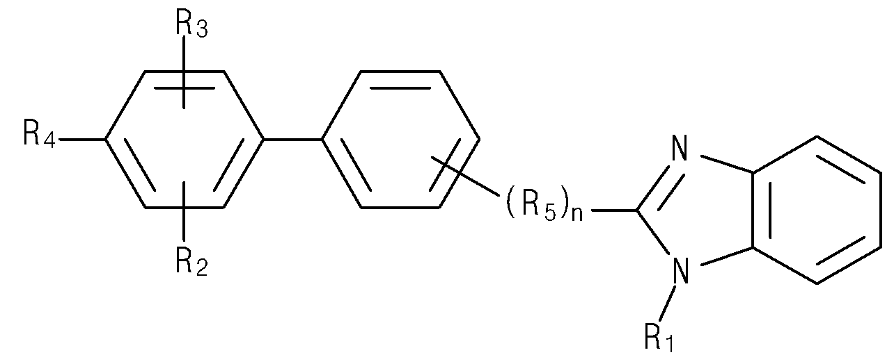
상기 화학식3에서, R1, R4 각각은 독립적으로 C6~C30의 아로마틱 그룹에서 선택되고, R2, R3 각각은 독립적으로 수소, C6~C30의 아로마틱 그룹에서 선택되며, R5는 C1~C10의 알킬에서 선택되고, n은 0 또는 1이다. R1은 벤젠일 수 있고, R4는 벤젠, 나프탈렌, 안트라센 중 어느 하나일 수 있다.In Formula 3, each of R1 and R4 is independently selected from an aromatic group of C6~C30, each of R2 and R3 is independently selected from an aromatic group of hydrogen and C6~C30, and R5 is selected from a group of C1~C10 alkyl and n is 0 or 1. R1 may be benzene, and R4 may be any one of benzene, naphthalene, and anthracene.
예를 들어, 전자 수송층(128)을 이루는 전자 수송 물질은 아래 화학식4의 화합물일 수 있다.For example, the electron transport material constituting the
[화학식4][Formula 4]

전자 수송층(128)이 화학식3의 전자 수송 물질로 이루어지는 경우, 적색 및 녹색 화소영역(Rp, Bp)에서 전자와 정공의 재결합이 적색 및 녹색 발광층(122, 124)에서 일어나기 때문에, 청색 피크 없이 고색순도의 적색 및 녹색 발광이 이루어진다.When the
한편, 청색 화소영역(Bp)에서는 청색 공통 발광층(126)이 정공 수송층(112)과 접하여 위치하기 때문에, 전자 수송층(128)이 전자 이동도가 높은 화학식3의 전자 수송 물질로 이루어지는 경우 청색 화소영역(Bp)에서의 발광은 정공 수송층(112)과 청색 공통 발광층(126)의 계면에서 일어난다. 따라서, 청색 화소영역(Bp)의 색 특성이 저하되는 문제가 발생한다.Meanwhile, in the blue pixel region Bp, since the blue
-제 2 실시예--Second embodiment-
도 6은 본 발명의 제 2 실시예에 따른 유기발광다이오드의 개략적인 단면도이다.6 is a schematic cross-sectional view of an organic light emitting diode according to a second embodiment of the present invention.
도 6에 도시한 바와 같이, 본 발명의 제 2 실시예에 따른 유기발광다이오드(D2)는 제 1 전극(210)과, 적색, 녹색, 청색 화소영역(Rp, Gp, Bp) 모두에 순차 적층되는 정공 주입층(211)과, 상기 적색 및 녹색 화소영역(Rp, Gp)에 형성되는 제 1 정공 수송층(214)과 상기 청색 화소영역(Bp)에 형성되는 제 2 정공 수송층(216)을 포함하는 정공 수송층(212)과, 상기 적색 화소영역(Rp)에 형성되는 적색 발광층(222), 상기 녹색 화소영역(Gp)에 형성되는 녹색 발광층(224) 및 상기 적색, 녹색, 청색 화소영역(Rp, Gp, Bp) 모두에 형성되는 청색 공통 발광층(226)을 포함하는 발광 물질층(220)과, 상기 청색 공통 발광층(226) 상에 형성되는 전자 수송층(228) 및 상기 전자 수송층(228) 상에 형성되는 제 2 전극(240)을 포함한다.As shown in FIG. 6 , the organic light emitting diode D2 according to the second embodiment of the present invention is sequentially stacked on the
여기서, 상기 정공 주입층(211), 상기 정공 수송층(212), 상기 발광 물질층(220), 상기 전자 수송층(228)은 유기 발광층(230)을 이룬다. Here, the
상기 유기 발광층(230) 중 상기 정공 주입층(211)과, 상기 정공 수송층(212)과, 상기 적색 발광층(222) 및 상기 녹색 발광층(224)은 용액 공정(solution process)에 의해 형성되고 상기 청색 공통 발광층(226) 및 상기 전자 수송층(228)은 증착 공정(deposition process)에 의해 형성된다.Among the organic emission layers 230 , the
상기 제 1 정공 수송층(214)은 정공 수송 물질(미도시)로 이루어지고, 상기 제 2 정공 수송층(214)은 정공 수송 물질과 도펀트(218)를 포함한다.The first
상기 도펀트(218)는 최저준위 비점유 분자괘도(Lowest Unoccupied Molecular Orbital, LUMO) 레벨이 청색 공통 발광층(226)의 LUMO 레벨보다 크고 1.0*E(-5) cm2/Vs 이상의 정공 이동도(hole mobility, μh)를 가질 수 있다. 이에 따라, 제 2 정공 수송층(216)은 청색 공통 발광층(226)으로부터의 전자 블로킹 역할을 하며 정공 주입층(221)으로부터의 정공을 청색 공통 발광층(226)으로 효율적으로 전달할 수 있다.The
바람직하게는, 상기 도펀트(218)는 1.0*E(-3) cm2/Vs보다 작고 1.0*E(-5) cm2/Vs보다 큰 정공 이동도를 가질 수 있다. (μh=1.0*E(-5) cm2/Vs~1.0*E(-3) cm2/Vs)Preferably, the

표1에서 보여지는 바와 같이, 상기 도펀트(218)의 정공 이동도가 1.0*E(-5) cm2/Vs보다 작은 경우 청색 화소영역(Bp)에서의 재결합 영역이 제 2 정공 수송층(216)으로 이동하여 청색 화소영역(Bp)의 색 특성이 저하된다. 한편, 상기 도펀트(218)의 정공 이동도가 1.0*E(-3) cm2/Vs보다 큰 경우 전하 균형이 저하되어 적색 및 녹색 화소영역(Rp, Gp)에서의 발광 효율이 저하된다.As shown in Table 1, when the hole mobility of the
또한, 상기 도펀트(218)는 2.0~2.5eV의 LUMO 값을 가질 수 있다. LUMO 값이 2.0eV보다 작으면 전자 블로킹 특성이 저하되고 2.5eV보다 크면 청색 화소영역(Bp)에서의 전하 균형(charge balance)이 저하되어, 청색 화소영역(Bp)의 발광 효율이 저하된다. Also, the
또한, 상기 도펀트(218)는 5.0~5.5eV의 최고준위 점유 분자괘도(Highest Occupied Molecular Orbital, HOMO) 레벨을 가질 수 있다. HOMO 값이 5.0eV보다 작거나 5.5eV보다 클 경우 정공과 전자의 재결합 영역이 정공 주입층(221) 또는 전자 수송층(228)에서 일어날 수 있다.Also, the
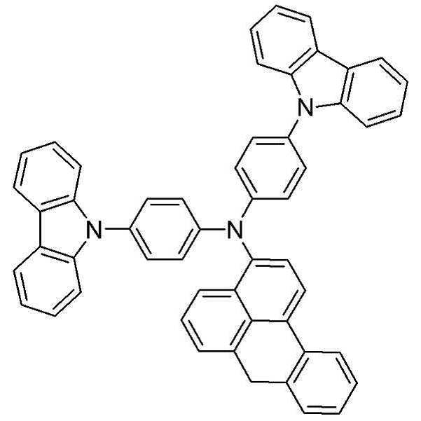
상기 도펀트(218)는 하기 화학식5로 표시될 수 있다.The
[화학식5][Formula 5]

상기 화학식5에서, R1, R2 각각은 독립적으로 이미다졸(imidazole) 그룹, 카바졸(carbazole) 그룹, 아민(amine) 그룹에서 선택될 수 있고, R3는 수소, C1~C60의 알킬 그룹, C6~C14의 아로마틱 그룹에서 선택될 수 있다.In Formula 5, each of R1 and R2 may be independently selected from an imidazole group, a carbazole group, and an amine group, and R3 is hydrogen, a C1-C60 alkyl group, C6- It may be selected from the aromatic group of C14.
예를 들어, 상기 도펀트(218)는 하기 화학식6에 표시된 물질일 수 있다.For example, the
[화학식6][Formula 6]

합성예Synthesis example
(1) 화합물A (1) Compound A
[반응식1][Scheme 1]

9-H-carbazol(5g), 1-chloro-4-iodobenzene(10.7g), Cu 파우더(powder) (0.2g), Na2SO4(4.2g), K2CO3(4.1g)을 190℃ 조건에서 12시간 환류, 교반하여 화합물A(9-(4-chlorophenyl)-9H-carbazole)를 얻었다. 190 9-H-carbazol (5g), 1-chloro-4-iodobenzene (10.7g), Cu powder (0.2g), Na 2 SO 4 (4.2g), K 2 CO 3 (4.1g) The mixture was refluxed and stirred at ℃ for 12 hours to obtain compound A (9-(4-chlorophenyl)-9H-carbazole).
(2) 화학식6의 화합물(2) a compound of formula (6)
[반응식2][Scheme 2]

Ar 조건에서, 화합물A(3g), Pd(t-bu)3(0.0064g), Pd(OAC)2 (0.0042g)을 toluene(5ml)에 넣고 용해시켰다. 7H-benzo[de]anthracen-3-amine(0.13g)을 혼합물에 넣어 반응시키고, 컬럼 크로마토그래피(ethylacetate:heaxane=2:1)를 통해 분리하여 화학식6 화합물(N,N-bis(4-(9H-carbazol-9-yl)phenyl)-7H-benzo[de]anthracen-3-amine)을 합성하였다.Under Ar conditions, Compound A (3 g), Pd(t-bu) 3 (0.0064 g), and Pd(OAC) 2 (0.0042 g) were dissolved in toluene (5 ml). 7H-benzo [de] anthracen-3-amine (0.13 g) was added to the mixture and reacted, separated through column chromatography (ethylacetate: heaxane = 2:1), and the compound of formula 6 (N, N-bis (4- (9H-carbazol-9-yl)phenyl)-7H-benzo[de]anthrcen-3-amine) was synthesized.
OLEDOLED
(1) 실험예1(1) Experimental Example 1
ITO 기판의 발광 면적이 3 mm X 3 mm 크기가 되도록 패터닝한 후 세정하였다. 다음, 상기 기판을 진공 증착 챔버 내로 이송하였다. 베이스 압력이 약 10-6 ~ 10-7 Torr가 되도록 한 후 양극인 ITO 위에, i) 정공주입층 (40nm, poly(3,4-ethylenedioxythiophene) polystyrene sulfonate(PEDOT:PSS)), ii) 정공수송층 (20nm, N,N’-di(1-naphthyl)-N,N’-diphenyl-(1,1’-biphenyl)-4,4’-diamine (NPB))을 코팅하고, iii) 청색 공통 발광층 (50nm, 호스트(N,N’-dicarbazolyl-3,5-benzene,4,4’,4’’-tris(N-carbazolyl)triphenylamine (TCTA):1,3,5-tri(m-pyrid-3-yl-phenyl)benzene(TmPyPb) (1:1)/도펀트(1,6-dihydro-2,7-diisopropylpyrene, 5%)), iv) 전자 수송층 (100nm, 2-(4-(10-(naphthalen-2-yl)-9-(naphthalen-3-yl)anthrace-3-yl)phenyl)-1-phenyl-1H-benzo[d]imidazole), v) 음극 (Al)을 순차 적층하였다.After patterning so that the emission area of the ITO substrate was 3 mm X 3 mm in size, it was washed. Next, the substrate was transferred into a vacuum deposition chamber. After the base pressure is about 10 -6 ~ 10 -7 Torr, on the anode, ITO, i) hole injection layer (40 nm, poly(3,4-ethylenedioxythiophene) polystyrene sulfonate (PEDOT:PSS)), ii) hole transport layer (20nm, N,N'-di(1-naphthyl)-N,N'-diphenyl-(1,1'-biphenyl)-4,4'-diamine (NPB)) was coated, iii) blue common emission layer (50nm, host (N,N'-dicarbazolyl-3,5-benzene,4,4',4''-tris(N-carbazolyl)triphenylamine (TCTA):1,3,5-tri(m-pyrid-) 3-yl-phenyl)benzene(TmPyPb) (1:1)/dopant (1,6-dihydro-2,7-diisopropylpyrene, 5%)), iv) electron transport layer (100nm, 2-(4-(10-) (naphthalen-2-yl)-9-(naphthalen-3-yl)anthrace-3-yl)phenyl)-1-phenyl-1H-benzo[d]imidazole), v) an anode (Al) was sequentially stacked.
(2) 실험예2(2) Experimental Example 2
실험예1의 정공 수송층에 도펀트(N3,N3-bis(4-(9H-carbazol-9-yl)phenyl)-N9,N9-dimethyl-7H-benzo[de]anthracene-3,9-diamine, 3%)를 도핑하였다.Dopant (N3,N3-bis(4-(9H-carbazol-9-yl)phenyl)-N9,N9-dimethyl-7H-benzo[de]anthracene-3,9-diamine, 3 in the hole transport layer of Experimental Example 1 %) was doped.
위 유기발광다이오드의 색좌표를 표2에 기재하였고, 발광 스펙트럼을 도 7에 도시하였다.The color coordinates of the above organic light emitting diode are described in Table 2, and the emission spectrum is shown in FIG.

표2 및 도 7에서 보여지는 바와 같이, 청색 화소영역(Bp)에 형성되는 제 2 정공 수송층(216)이 화학식5에 표시되는 도펀트(218)를 포함하는 경우, 청색 화소영역(Bp)의 색 특성이 개선된다.As shown in Table 2 and FIG. 7 , when the second hole transport layer 216 formed in the blue pixel region Bp includes the
보다 구체적으로 유기발광다이오드(D3)의 제조 방법을 설명한다.More specifically, a method of manufacturing the organic light emitting diode D3 will be described.
먼저, 기판(도 4의 150) 상부에 ITO와 같은 투명 도전성 물질을 증착하고 각 화소영역 별로 패터닝하여 적색, 녹색 및 청색 화소영역(Rp, Gp, Bp)에 상기 제 1 전극(210)을 형성한다.First, a transparent conductive material such as ITO is deposited on a substrate (150 in FIG. 4) and patterned for each pixel region to form the
다음, 상기 제 1 전극(210) 상에 정공 주입 물질을 코팅하여 상기 적색, 녹색 및 청색 화소영역(Rp, Gp, Bp)에 정공 주입층(211)을 형성한다. Next, a
다음, 상기 정공 주입층(211) 상에 정공 수송 물질을 코팅하여 적색 및 녹색 화소영역(Rp, Gp)에 제 1 정공 수송층(214)를 형성하고, 상기 정공 주입층(211) 상에 정공 수송 물질과 화학식1에 표시된 도펀트(218)를 코팅하여 청색 화소영역(Bp)에 제 2 정공 수송층(216)을 형성한다. 이후, 소성 공정을 진행한다. Next, a first
다음, 제 1 정공 수송층(214) 상에, 적색 발광 물질과 녹색 발광 물질을 코팅하여 상기 적색 화소영역(Rp) 및 상기 녹색 화소영역(Gp) 각각에 적색 발광층(222)과 녹색 발광층(224)을 형성한다.Next, a red light emitting material and a green light emitting material are coated on the first
다음, 청색 발광 물질, 전자 수송 물질 및 알루미늄과 같은 금속 물질을 순차 증착하여 상기 적색, 녹색 및 청색 화소영역(Rp, Gp, Bp) 모두에 대응하여 청색 공통 발광층(226)과 전자 수송층(228) 및 제 2 전극(240)을 형성한다.Next, a blue light emitting material, an electron transporting material, and a metal material such as aluminum are sequentially deposited to correspond to all of the red, green, and blue pixel regions Rp, Gp, and Bp. A blue
이와 같이, 하이브리드 구조 유기발광다이오드(D3)에서는, 상기 정공 주입층(211)과, 상기 제 1 및 제 2 정공 수송층(214, 216)과, 상기 적색 발광층(222) 및 상기 녹색 발광층(224)이 용액 공정에 의해 형성되기 때문에, 유기발광다이오드(D2)의 제조 비용이 절감되고 대면적 표시장치를 제공할 수 있다.As such, in the hybrid structure organic light emitting diode D3, the
또한, 적색 및 녹색 화소영역(Rp, Gp) 각각에서 발광이 적색 및 녹색 발광층(222, 224)에서 일어나도록 하기 위해 높은 전자 이동도를 갖는 물질로 전자 수송층(228)을 형성하고, 청색 화소영역(Bp)의 제 2 정공 수송층(216)이 도펀트(218)를 포함함으로써 청색 화소영역(Bp)에서의 색 특성을 개선할 수 있다.In addition, the
따라서, 제조 원가가 절감되고 우수한 색 특성을 갖는 유기발광다이오드를 제공할 수 있다.Accordingly, it is possible to reduce the manufacturing cost and provide an organic light emitting diode having excellent color characteristics.
상기에서는 본 발명의 바람직한 실시예를 참조하여 설명하였지만, 해당 기술분야의 통상의 기술자는 하기의 특허청구범위에 기재된 본 발명의 기술적 사상 및 영역으로부터 벗어나지 않는 범위 내에서 본 발명을 다양하게 수정 및 변경시킬 수 있음을 이해할 수 있을 것이다.Although the above has been described with reference to the preferred embodiment of the present invention, those skilled in the art can variously modify and change the present invention within the scope without departing from the spirit and scope of the present invention described in the claims below. You will understand that it can be done.
110, 210: 제 1 전극 111, 211: 정공 주입층
112, 212, 214, 216: 정공 수송층
218: 도펀트 120, 220: 발광 물질층
122, 222: 적색 발광층 124, 224: 녹색 발광층
126, 226: 청색 공통 발광층 128, 228: 전자 수송층
140, 240: 제 2 전극 D1, D2: 유기발광다이오드110, 210:
112, 212, 214, 216: hole transport layer
218:
122, 222: red light-emitting
126, 226: blue
140, 240: second electrode D1, D2: organic light emitting diode
Claims (11)
상기 적색, 녹색 및 청색 화소영역에 대응하여 상기 제 1 전극 상에 위치하는 정공 주입층과;
상기 적색 및 녹색 화소영역에 대응하여 상기 정공 주입층 상에 위치하는 제 1 정공 수송층과;
상기 청색 화소영역에 대응하여 상기 정공 주입층 상에 위치하는 제 2 정공 수송층과;
상기 적색 및 녹색 화소영역 각각에 대응하여 상기 제 1 정공 수송층 상에 위치하는 적색 및 녹색 발광층과;
상기 적색 및 녹색 발광층과 상기 제 2 정공 수송층 상에 위치하는 청색 공통 발광층과;
상기 청색 공통 발광층 상에 순차 적층되는 전자 수송층 및 제 2 전극을 포함하고,
상기 제 2 정공 수송층은 정공 수송 물질과 1.0*E(-3) cm2/Vs보다 작고 1.0*E(-5) cm2/Vs보다 큰 정공 이동도를 갖는 도펀트를 포함하며,
상기 전자 수송층은 하기 화학식1로 표시되는 물질을 포함하고,
화학식1에서, R1, R4 각각은 독립적으로 C6~C30의 아로마틱 그룹에서 선택되며, R2, R3 각각은 독립적으로 수소, C6~C30의 아로마틱 그룹에서 선택되고, R5는 C1~C10의 알킬에서 선택되며, n은 0 또는 1이고,
상기 도펀트는 하기 화학식2로 표시되며,
화학식2에서, R1, R2 각각은 독립적으로 이미다졸 그룹, 카바졸 그룹, 아민 그룹에서 선택되고, R3는 수소, C1~C60의 알킬 그룹, C6~C14의 아로마틱 그룹에서 선택되는 유기발광다이오드.
[화학식1]

[화학식2]

a first electrode positioned on a substrate in which red, green, and blue pixel regions are defined for each of the red, green, and blue pixel regions;
a hole injection layer positioned on the first electrode corresponding to the red, green, and blue pixel regions;
a first hole transport layer positioned on the hole injection layer corresponding to the red and green pixel regions;
a second hole transport layer positioned on the hole injection layer corresponding to the blue pixel region;
red and green light emitting layers positioned on the first hole transport layer corresponding to the red and green pixel regions, respectively;
a blue common emission layer disposed on the red and green emission layers and the second hole transport layer;
an electron transport layer and a second electrode sequentially stacked on the blue common light emitting layer;
The second hole transport layer comprises a hole transport material and a dopant having a hole mobility of less than 1.0*E(-3) cm 2 /Vs and greater than 1.0*E(-5) cm 2 /Vs,
The electron transport layer includes a material represented by the following formula (1),
In Formula 1, each of R1 and R4 is independently selected from an aromatic group of C6 to C30, each of R2 and R3 is independently selected from an aromatic group of hydrogen, C6 to C30, R5 is selected from an alkyl of C1 to C10, , n is 0 or 1,
The dopant is represented by the following formula (2),
In Formula 2, each of R1 and R2 is independently selected from an imidazole group, a carbazole group, and an amine group, and R3 is hydrogen, a C1-C60 alkyl group, and a C6-C14 aromatic group.
[Formula 1]
[Formula 2]
상기 적색, 녹색 및 청색 화소영역에 대응하여 상기 제 1 전극 상에 위치하는 정공 주입층과;
상기 적색 및 녹색 화소영역에 대응하여 상기 정공 주입층 상에 위치하는 제 1 정공 수송층과;
상기 청색 화소영역에 대응하여 상기 정공 주입층 상에 위치하는 제 2 정공 수송층과;
상기 적색 및 녹색 화소영역 각각에 대응하여 상기 제 1 정공 수송층 상에 위치하는 적색 및 녹색 발광층과;
상기 적색 및 녹색 발광층과 상기 제 2 정공 수송층 상에 위치하는 청색 공통 발광층과;
상기 청색 공통 발광층 상에 순차 적층되는 전자 수송층 및 제 2 전극을 포함하고,
상기 제 2 정공 수송층은 정공 수송 물질과 1.0*E(-3) cm2/Vs보다 작고 1.0*E(-5) cm2/Vs보다 큰 정공 이동도를 갖는 도펀트를 포함하며,
상기 전자 수송층의 물질은 하기 화합물1이고, 상기 도펀트는 하기 화합물2인 유기발광다이오드.
[화합물1]

[화합물2]

a first electrode positioned on a substrate in which red, green, and blue pixel regions are defined for each of the red, green, and blue pixel regions;
a hole injection layer positioned on the first electrode corresponding to the red, green, and blue pixel regions;
a first hole transport layer positioned on the hole injection layer corresponding to the red and green pixel regions;
a second hole transport layer positioned on the hole injection layer corresponding to the blue pixel region;
red and green light emitting layers positioned on the first hole transport layer corresponding to the red and green pixel regions, respectively;
a blue common emission layer disposed on the red and green emission layers and the second hole transport layer;
an electron transport layer and a second electrode sequentially stacked on the blue common light emitting layer;
The second hole transport layer comprises a hole transport material and a dopant having a hole mobility of less than 1.0*E(-3) cm 2 /Vs and greater than 1.0*E(-5) cm 2 /Vs,
The material of the electron transport layer is the following compound 1, and the dopant is the following compound 2 organic light emitting diode.
[Compound 1]
[Compound 2]
상기 도펀트의 최저준위 비점유 분자괘도(LUMO) 레벨은 상기 청색 공통 발광층의 LUMO 레벨보다 큰 유기발광다이오드.
3. The method according to claim 1 or 2,
The lowest unoccupied molecular orbital (LUMO) level of the dopant is greater than the LUMO level of the blue common emission layer.
상기 도펀트는 2.0~2.5eV의 LUMO 값을 갖는 유기발광다이오드.
4. The method of claim 3,
The dopant is an organic light emitting diode having a LUMO value of 2.0 to 2.5 eV.
상기 정공 주입층과, 상기 제 1 및 제 2 정공 수송층과, 상기 적색 발광층 및 상기 녹색 발광층은 용액 공정에 의해 형성되고, 상기 청색 공통 발광층과 상기 전자 수송층은 증착 공정에 의해 형성되는 유기발광다이오드.
3. The method according to claim 1 or 2,
The hole injection layer, the first and second hole transport layers, the red emission layer and the green emission layer are formed by a solution process, and the blue common emission layer and the electron transport layer are formed by a deposition process.
상기 제 1 전극 상에 정공 주입 물질을 코팅하여, 상기 적색, 녹색 및 청색 화소영역에 대응하는 정공 주입층을 형성하는 단계와;
상기 정공 주입층 상에 정공 수송 물질을 코팅하여 상기 적색 및 녹색 화소영역에 대응하는 제 1 정공 수송층을 형성하는 단계와;
상기 정공 주입층 상에 상기 정공 수송 물질과 도펀트를 코팅하여 상기 청색 화소영역에 대응하는 제 2 정공 수송층을 형성하는 단계와;
상기 적색 및 녹색 화소영역 각각에 대응하여 상기 제 1 정공 수송층 상에 적색 및 녹색 발광층을 코팅하는 단계와;
상기 적색 및 녹색 발광층과 상기 제 2 정공 수송층 상에 청색 공통 발광층을 증착하는 단계와;
상기 청색 공통 발광층 상에 전자 수송층을 순차 증착하는 단계와;
상기 전자 수송층 상에 제 2 전극을 형성하는 단계를 포함하고,
상기 도펀트는 1.0*E(-3) cm2/Vs보다 작고 1.0*E(-5) cm2/Vs보다 큰 정공 이동도를 가지며,
상기 전자 수송층은 하기 화학식1로 표시되는 물질을 포함하고,
화학식1에서, R1, R4 각각은 독립적으로 C6~C30의 아로마틱 그룹에서 선택되며, R2, R3 각각은 독립적으로 수소, C6~C30의 아로마틱 그룹에서 선택되고, R5는 C1~C10의 알킬에서 선택되며, n은 0 또는 1이고,
상기 도펀트는 하기 화학식2로 표시되며,
화학식2에서, R1, R2 각각은 독립적으로 이미다졸 그룹, 카바졸 그룹, 아민 그룹에서 선택되고, R3는 수소, C1~C60의 알킬 그룹, C6~C14의 아로마틱 그룹에서 선택되는 유기발광다이오드의 제조 방법.
[화학식1]

[화학식2]
forming a first electrode for each red, green, and blue pixel region on a substrate in which red, green, and blue pixel regions are defined;
forming a hole injection layer corresponding to the red, green, and blue pixel regions by coating a hole injection material on the first electrode;
forming a first hole transport layer corresponding to the red and green pixel regions by coating a hole transport material on the hole injection layer;
forming a second hole transport layer corresponding to the blue pixel region by coating the hole transport material and a dopant on the hole injection layer;
coating red and green light emitting layers on the first hole transport layer corresponding to each of the red and green pixel regions;
depositing a blue common emission layer on the red and green emission layers and the second hole transport layer;
sequentially depositing an electron transport layer on the blue common emission layer;
forming a second electrode on the electron transport layer;
The dopant has a hole mobility smaller than 1.0*E(-3) cm 2 /Vs and greater than 1.0*E(-5) cm 2 /Vs,
The electron transport layer includes a material represented by the following formula (1),
In Formula 1, each of R1 and R4 is independently selected from an aromatic group of C6 to C30, each of R2 and R3 is independently selected from an aromatic group of hydrogen, C6 to C30, R5 is selected from an alkyl of C1 to C10, , n is 0 or 1,
The dopant is represented by the following formula (2),
In Formula 2, each of R1 and R2 is independently selected from an imidazole group, a carbazole group, and an amine group, and R3 is hydrogen, a C1-C60 alkyl group, and a C6-C14 aromatic group. method.
[Formula 1]
[Formula 2]
상기 제 1 전극 상에 정공 주입 물질을 코팅하여, 상기 적색, 녹색 및 청색 화소영역에 대응하는 정공 주입층을 형성하는 단계와;
상기 정공 주입층 상에 정공 수송 물질을 코팅하여 상기 적색 및 녹색 화소영역에 대응하는 제 1 정공 수송층을 형성하는 단계와;
상기 정공 주입층 상에 상기 정공 수송 물질과 도펀트를 코팅하여 상기 청색 화소영역에 대응하는 제 2 정공 수송층을 형성하는 단계와;
상기 적색 및 녹색 화소영역 각각에 대응하여 상기 제 1 정공 수송층 상에 적색 및 녹색 발광층을 코팅하는 단계와;
상기 적색 및 녹색 발광층과 상기 제 2 정공 수송층 상에 청색 공통 발광층을 증착하는 단계와;
상기 청색 공통 발광층 상에 전자 수송층을 순차 증착하는 단계와;
상기 전자 수송층 상에 제 2 전극을 형성하는 단계를 포함하고,
상기 도펀트는 1.0*E(-3) cm2/Vs보다 작고 1.0*E(-5) cm2/Vs보다 큰 정공 이동도를 가지며,
상기 전자 수송층의 물질은 하기 화합물1이고, 상기 도펀트는 하기 화합물2인 유기발광다이오드의 제조 방법.
[화합물1]

[화합물2]
forming a first electrode for each red, green, and blue pixel region on a substrate in which red, green, and blue pixel regions are defined;
forming a hole injection layer corresponding to the red, green, and blue pixel regions by coating a hole injection material on the first electrode;
forming a first hole transport layer corresponding to the red and green pixel regions by coating a hole transport material on the hole injection layer;
forming a second hole transport layer corresponding to the blue pixel region by coating the hole transport material and a dopant on the hole injection layer;
coating red and green light emitting layers on the first hole transport layer corresponding to each of the red and green pixel regions;
depositing a blue common emission layer on the red and green emission layers and the second hole transport layer;
sequentially depositing an electron transport layer on the blue common emission layer;
forming a second electrode on the electron transport layer;
The dopant has a hole mobility smaller than 1.0*E(-3) cm 2 /Vs and greater than 1.0*E(-5) cm 2 /Vs,
The material of the electron transport layer is the following compound 1, and the dopant is the following compound 2 method of manufacturing an organic light emitting diode.
[Compound 1]
[Compound 2]
상기 도펀트의 최저준위 비점유 분자괘도(LUMO) 레벨은 상기 청색 공통 발광층의 LUMO 레벨보다 큰 유기발광다이오드의 제조 방법.
9. The method according to claim 7 or 8,
The lowest unoccupied molecular orbital (LUMO) level of the dopant is greater than the LUMO level of the blue common emission layer.
상기 도펀트는 2.0~2.5eV의 LUMO 값을 갖는 유기발광다이오드의 제조 방법.
10. The method of claim 9,
The dopant is a method of manufacturing an organic light emitting diode having a LUMO value of 2.0 to 2.5 eV.
Priority Applications (1)
| Application Number | Priority Date | Filing Date | Title |
|---|---|---|---|
| KR1020170064300A KR102285867B1 (en) | 2015-11-30 | 2017-05-24 | Organic light emitting diode and method of fabricating the same |
Applications Claiming Priority (2)
| Application Number | Priority Date | Filing Date | Title |
|---|---|---|---|
| KR1020150169500A KR20170063290A (en) | 2015-11-30 | 2015-11-30 | Organic light emitting diode and method of fabricating the same |
| KR1020170064300A KR102285867B1 (en) | 2015-11-30 | 2017-05-24 | Organic light emitting diode and method of fabricating the same |
Related Parent Applications (1)
| Application Number | Title | Priority Date | Filing Date |
|---|---|---|---|
| KR1020150169500A Division KR20170063290A (en) | 2015-11-30 | 2015-11-30 | Organic light emitting diode and method of fabricating the same |
Publications (2)
| Publication Number | Publication Date |
|---|---|
| KR20170063480A KR20170063480A (en) | 2017-06-08 |
| KR102285867B1 true KR102285867B1 (en) | 2021-08-03 |
Family
ID=59221601
Family Applications (1)
| Application Number | Title | Priority Date | Filing Date |
|---|---|---|---|
| KR1020170064300A Active KR102285867B1 (en) | 2015-11-30 | 2017-05-24 | Organic light emitting diode and method of fabricating the same |
Country Status (1)
| Country | Link |
|---|---|
| KR (1) | KR102285867B1 (en) |
Family Cites Families (4)
| Publication number | Priority date | Publication date | Assignee | Title |
|---|---|---|---|---|
| KR101950827B1 (en) * | 2011-12-21 | 2019-04-26 | 엘지디스플레이 주식회사 | Organic Light Emitting Device and Method for Manufacturing the Same |
| KR102053443B1 (en) * | 2013-10-23 | 2019-12-06 | 엘지디스플레이 주식회사 | Organic light emitting device |
| KR102113491B1 (en) * | 2013-12-31 | 2020-05-22 | 엘지디스플레이 주식회사 | Organic Light Emitting Display Device |
| US9905785B2 (en) * | 2014-04-14 | 2018-02-27 | Universal Display Corporation | Organic electroluminescent materials and devices |
-
2017
- 2017-05-24 KR KR1020170064300A patent/KR102285867B1/en active Active
Also Published As
| Publication number | Publication date |
|---|---|
| KR20170063480A (en) | 2017-06-08 |
Similar Documents
| Publication | Publication Date | Title |
|---|---|---|
| CN112514094B (en) | Organic light emitting diode and organic light emitting device including the same | |
| KR101703174B1 (en) | Organic light emitting diode and method of fabricating the same | |
| KR102546673B1 (en) | Organic light emitting device and display device having the same | |
| JP5196928B2 (en) | Organic light emitting device and display device | |
| KR20080086825A (en) | Light emitting device and electronic device | |
| US20220020945A1 (en) | Color stable organic light emitting diode stack | |
| CN108117540B (en) | Organic compound, organic light emitting diode, and organic light emitting display device | |
| KR102237159B1 (en) | Organic Compound and Organic Light Emitting Diode Devices using the same | |
| CN110590755B (en) | Space charge transfer compound, organic light emitting diode and display device | |
| WO2022007177A1 (en) | Organic light-emitting diode display device and manufacturing method therefor, and display panel | |
| KR102674792B1 (en) | Organic light emitting diode and Organic light emitting display device including the same | |
| WO2011024346A1 (en) | Organic electroluminescent element, organic electroluminescent display device, and organic electroluminescent illuminating device | |
| CN111320639B (en) | Organic compound, organic light emitting diode and organic light emitting display device | |
| CN110551110B (en) | Space charge transfer compound, and organic light emitting diode and organic light emitting display device including the same | |
| KR20170063290A (en) | Organic light emitting diode and method of fabricating the same | |
| KR102285867B1 (en) | Organic light emitting diode and method of fabricating the same | |
| CN114583070B (en) | Organic light emitting diode and organic light emitting device including the same | |
| KR102390699B1 (en) | Organic light emitting diode | |
| KR102829508B1 (en) | Organic compounds, organic light emitting diode and organic light emitting display device including the compounds | |
| KR20190064202A (en) | Organic compounds, organic light emitting diode and orgnic light emitting display device including the compounds | |
| US20240244949A1 (en) | Organometallic compound and organic light emitting diode comprising the same | |
| US20240244948A1 (en) | Organometallic compound and organic light emitting diode comprising the same | |
| US20240244946A1 (en) | Organic light emitting diode comprising organometallic compound and plurality of host materials | |
| US20240244864A1 (en) | Organometallic compound and organic light emitting diode comprising the same | |
| US20240260295A1 (en) | Organic light emitting diode comprising organometallic compound and plurality of host materials |
Legal Events
| Date | Code | Title | Description |
|---|---|---|---|
| A107 | Divisional application of patent | ||
| PA0107 | Divisional application |
St.27 status event code: A-0-1-A10-A18-div-PA0107 St.27 status event code: A-0-1-A10-A16-div-PA0107 |
|
| PG1501 | Laying open of application |
St.27 status event code: A-1-1-Q10-Q12-nap-PG1501 |
|
| A201 | Request for examination | ||
| PA0201 | Request for examination |
St.27 status event code: A-1-2-D10-D11-exm-PA0201 |
|
| E902 | Notification of reason for refusal | ||
| PE0902 | Notice of grounds for rejection |
St.27 status event code: A-1-2-D10-D21-exm-PE0902 |
|
| E13-X000 | Pre-grant limitation requested |
St.27 status event code: A-2-3-E10-E13-lim-X000 |
|
| P11-X000 | Amendment of application requested |
St.27 status event code: A-2-2-P10-P11-nap-X000 |
|
| P13-X000 | Application amended |
St.27 status event code: A-2-2-P10-P13-nap-X000 |
|
| E701 | Decision to grant or registration of patent right | ||
| PE0701 | Decision of registration |
St.27 status event code: A-1-2-D10-D22-exm-PE0701 |
|
| GRNT | Written decision to grant | ||
| PR0701 | Registration of establishment |
St.27 status event code: A-2-4-F10-F11-exm-PR0701 |
|
| PR1002 | Payment of registration fee |
St.27 status event code: A-2-2-U10-U11-oth-PR1002 Fee payment year number: 1 |
|
| PG1601 | Publication of registration |
St.27 status event code: A-4-4-Q10-Q13-nap-PG1601 |
|
| P22-X000 | Classification modified |
St.27 status event code: A-4-4-P10-P22-nap-X000 |
|
| P22-X000 | Classification modified |
St.27 status event code: A-4-4-P10-P22-nap-X000 |
|
| PR1001 | Payment of annual fee |
St.27 status event code: A-4-4-U10-U11-oth-PR1001 Fee payment year number: 4 |
|
| P22-X000 | Classification modified |
St.27 status event code: A-4-4-P10-P22-nap-X000 |