KR102229648B1 - Apparatus and method of wear leveling for storage class memory - Google Patents
Apparatus and method of wear leveling for storage class memory Download PDFInfo
- Publication number
- KR102229648B1 KR102229648B1 KR1020197000678A KR20197000678A KR102229648B1 KR 102229648 B1 KR102229648 B1 KR 102229648B1 KR 1020197000678 A KR1020197000678 A KR 1020197000678A KR 20197000678 A KR20197000678 A KR 20197000678A KR 102229648 B1 KR102229648 B1 KR 102229648B1
- Authority
- KR
- South Korea
- Prior art keywords
- group
- memory
- write cache
- address
- logging
- Prior art date
- Legal status (The legal status is an assumption and is not a legal conclusion. Google has not performed a legal analysis and makes no representation as to the accuracy of the status listed.)
- Active
Links
Images


Classifications
-
- G—PHYSICS
- G06—COMPUTING OR CALCULATING; COUNTING
- G06F—ELECTRIC DIGITAL DATA PROCESSING
- G06F12/00—Accessing, addressing or allocating within memory systems or architectures
- G06F12/02—Addressing or allocation; Relocation
- G06F12/0223—User address space allocation, e.g. contiguous or non contiguous base addressing
- G06F12/023—Free address space management
- G06F12/0238—Memory management in non-volatile memory, e.g. resistive RAM or ferroelectric memory
-
- G—PHYSICS
- G06—COMPUTING OR CALCULATING; COUNTING
- G06F—ELECTRIC DIGITAL DATA PROCESSING
- G06F11/00—Error detection; Error correction; Monitoring
- G06F11/07—Responding to the occurrence of a fault, e.g. fault tolerance
- G06F11/08—Error detection or correction by redundancy in data representation, e.g. by using checking codes
- G06F11/10—Adding special bits or symbols to the coded information, e.g. parity check, casting out 9's or 11's
- G06F11/1008—Adding special bits or symbols to the coded information, e.g. parity check, casting out 9's or 11's in individual solid state devices
- G06F11/1068—Adding special bits or symbols to the coded information, e.g. parity check, casting out 9's or 11's in individual solid state devices in sector programmable memories, e.g. flash disk
-
- G—PHYSICS
- G06—COMPUTING OR CALCULATING; COUNTING
- G06F—ELECTRIC DIGITAL DATA PROCESSING
- G06F12/00—Accessing, addressing or allocating within memory systems or architectures
- G06F12/02—Addressing or allocation; Relocation
- G06F12/0223—User address space allocation, e.g. contiguous or non contiguous base addressing
- G06F12/023—Free address space management
- G06F12/0238—Memory management in non-volatile memory, e.g. resistive RAM or ferroelectric memory
- G06F12/0246—Memory management in non-volatile memory, e.g. resistive RAM or ferroelectric memory in block erasable memory, e.g. flash memory
-
- G—PHYSICS
- G06—COMPUTING OR CALCULATING; COUNTING
- G06F—ELECTRIC DIGITAL DATA PROCESSING
- G06F12/00—Accessing, addressing or allocating within memory systems or architectures
- G06F12/02—Addressing or allocation; Relocation
- G06F12/08—Addressing or allocation; Relocation in hierarchically structured memory systems, e.g. virtual memory systems
- G06F12/0802—Addressing of a memory level in which the access to the desired data or data block requires associative addressing means, e.g. caches
- G06F12/0804—Addressing of a memory level in which the access to the desired data or data block requires associative addressing means, e.g. caches with main memory updating
-
- G—PHYSICS
- G06—COMPUTING OR CALCULATING; COUNTING
- G06F—ELECTRIC DIGITAL DATA PROCESSING
- G06F12/00—Accessing, addressing or allocating within memory systems or architectures
- G06F12/02—Addressing or allocation; Relocation
- G06F12/08—Addressing or allocation; Relocation in hierarchically structured memory systems, e.g. virtual memory systems
- G06F12/10—Address translation
- G06F12/1009—Address translation using page tables, e.g. page table structures
-
- G—PHYSICS
- G06—COMPUTING OR CALCULATING; COUNTING
- G06F—ELECTRIC DIGITAL DATA PROCESSING
- G06F3/00—Input arrangements for transferring data to be processed into a form capable of being handled by the computer; Output arrangements for transferring data from processing unit to output unit, e.g. interface arrangements
- G06F3/06—Digital input from, or digital output to, record carriers, e.g. RAID, emulated record carriers or networked record carriers
- G06F3/0601—Interfaces specially adapted for storage systems
- G06F3/0602—Interfaces specially adapted for storage systems specifically adapted to achieve a particular effect
- G06F3/0614—Improving the reliability of storage systems
- G06F3/0619—Improving the reliability of storage systems in relation to data integrity, e.g. data losses, bit errors
-
- G—PHYSICS
- G06—COMPUTING OR CALCULATING; COUNTING
- G06F—ELECTRIC DIGITAL DATA PROCESSING
- G06F3/00—Input arrangements for transferring data to be processed into a form capable of being handled by the computer; Output arrangements for transferring data from processing unit to output unit, e.g. interface arrangements
- G06F3/06—Digital input from, or digital output to, record carriers, e.g. RAID, emulated record carriers or networked record carriers
- G06F3/0601—Interfaces specially adapted for storage systems
- G06F3/0628—Interfaces specially adapted for storage systems making use of a particular technique
- G06F3/0638—Organizing or formatting or addressing of data
- G06F3/064—Management of blocks
-
- G—PHYSICS
- G06—COMPUTING OR CALCULATING; COUNTING
- G06F—ELECTRIC DIGITAL DATA PROCESSING
- G06F3/00—Input arrangements for transferring data to be processed into a form capable of being handled by the computer; Output arrangements for transferring data from processing unit to output unit, e.g. interface arrangements
- G06F3/06—Digital input from, or digital output to, record carriers, e.g. RAID, emulated record carriers or networked record carriers
- G06F3/0601—Interfaces specially adapted for storage systems
- G06F3/0668—Interfaces specially adapted for storage systems adopting a particular infrastructure
- G06F3/0671—In-line storage system
- G06F3/0683—Plurality of storage devices
- G06F3/0685—Hybrid storage combining heterogeneous device types, e.g. hierarchical storage, hybrid arrays
-
- G—PHYSICS
- G11—INFORMATION STORAGE
- G11C—STATIC STORES
- G11C29/00—Checking stores for correct operation ; Subsequent repair; Testing stores during standby or offline operation
- G11C29/52—Protection of memory contents; Detection of errors in memory contents
-
- G—PHYSICS
- G06—COMPUTING OR CALCULATING; COUNTING
- G06F—ELECTRIC DIGITAL DATA PROCESSING
- G06F2212/00—Indexing scheme relating to accessing, addressing or allocation within memory systems or architectures
- G06F2212/10—Providing a specific technical effect
- G06F2212/1032—Reliability improvement, data loss prevention, degraded operation etc
- G06F2212/1036—Life time enhancement
-
- G—PHYSICS
- G06—COMPUTING OR CALCULATING; COUNTING
- G06F—ELECTRIC DIGITAL DATA PROCESSING
- G06F2212/00—Indexing scheme relating to accessing, addressing or allocation within memory systems or architectures
- G06F2212/40—Specific encoding of data in memory or cache
- G06F2212/403—Error protection encoding, e.g. using parity or ECC codes
-
- G—PHYSICS
- G06—COMPUTING OR CALCULATING; COUNTING
- G06F—ELECTRIC DIGITAL DATA PROCESSING
- G06F2212/00—Indexing scheme relating to accessing, addressing or allocation within memory systems or architectures
- G06F2212/60—Details of cache memory
- G06F2212/608—Details relating to cache mapping
-
- G—PHYSICS
- G06—COMPUTING OR CALCULATING; COUNTING
- G06F—ELECTRIC DIGITAL DATA PROCESSING
- G06F2212/00—Indexing scheme relating to accessing, addressing or allocation within memory systems or architectures
- G06F2212/72—Details relating to flash memory management
- G06F2212/7211—Wear leveling
-
- G—PHYSICS
- G11—INFORMATION STORAGE
- G11C—STATIC STORES
- G11C29/00—Checking stores for correct operation ; Subsequent repair; Testing stores during standby or offline operation
- G11C29/04—Detection or location of defective memory elements, e.g. cell constructio details, timing of test signals
- G11C2029/0409—Online test
Landscapes
- Engineering & Computer Science (AREA)
- Theoretical Computer Science (AREA)
- Physics & Mathematics (AREA)
- General Engineering & Computer Science (AREA)
- General Physics & Mathematics (AREA)
- Human Computer Interaction (AREA)
- Quality & Reliability (AREA)
- Computer Security & Cryptography (AREA)
- Memory System Of A Hierarchy Structure (AREA)
- Techniques For Improving Reliability Of Storages (AREA)
Abstract
저장 클래스 메모리용 웨어 레벨링의 방법 및 장치가 개시된다. 쓰기 캐시 히트에 대응하는 비휘발성 메모리에 쓰기될 현재 데이터가 결정된다. 쓰기 캐시 히트의 경우, 현재 데이터는 비휘발성 메모리의 예정 위치와 상이한 비휘발성 메모리의 지정 위치뿐만 아니라 쓰기 캐시에 쓰기된다. 쓰기 캐시 미스인 경우, 현재 데이터는 비휘발성 메모리의 예정 위치에 쓰기된다. 현재 데이터가 쓰기 캐시 미스에 대응하고 그리고 쓰기 캐시가 가득차지 않은 경우, 현재 데이터는 쓰기 캐시에 더 쓰기된다. 대안적으로, 현재 데이터는 비휘발성 메모리의 예정 위치와는 상이한 비휘발성 메모리의 지정 위치뿐만 아니라 쓰기 캐시에 쓰기된다. A method and apparatus for wear leveling for a storage class memory are disclosed. Current data to be written to the nonvolatile memory corresponding to the write cache hit is determined. In the case of a write cache hit, the current data is written to the write cache as well as a designated location in the non-volatile memory that is different from the predetermined location in the non-volatile memory. In the case of a write cache miss, the current data is written to a predetermined location in the nonvolatile memory. If the current data corresponds to a write cache miss and the write cache is not full, the current data is further written to the write cache. Alternatively, the current data is written to the write cache as well as a designated location in the non-volatile memory that is different from the predetermined location in the non-volatile memory.
Description
본 발명은 2016년 8월 6일자로 출원된 미국 정규출원 제 15/230,414호를 우선권으로 청구한다. 미국 정규출원은 그 전체가 본원에 참고로 인용된다. The present invention claims priority to US Regular Application No. 15/230,414, filed Aug. 6, 2016. US regular applications are incorporated herein by reference in their entirety.
본 발명은 메모리 제어에 관한 것이다. 특히, 본 발명은 메모리 장치의 내구성을 연장시키기 위한 메모리 장치의 웨어 레벨링(wear leveling)에 관한 것이다. The present invention relates to memory control. In particular, the present invention relates to wear leveling of a memory device to extend the durability of the memory device.
컴퓨터 구조에서 메모리 계층은 컴퓨터 아키텍쳐 설계, 알고리즘 예측 및 참조 지역성(locality of reference)과 같은 하위 레벨 프로그래밍 구성에서 성능 문제를 저장하고 논의하는데 사용되는 개념이다. 컴퓨터 저장소의 메모리 계층은 응답 시간으로 계층 구조의 각각의 레벨을 구별한다. 응답 시간, 복잡성 및 용량이 관련되어 상기 레벨은 그들의 성능 및 제어 기술로 더 구별될 수 있다. In computer architecture, the memory layer is a concept used to store and discuss performance problems in low-level programming constructs such as computer architecture design, algorithm prediction, and locality of reference. The memory hierarchy of the computer's storage distinguishes each level of the hierarchy by response time. Response times, complexity and capacity are related so the levels can be further distinguished by their performance and control techniques.
본 발명의 맥락에서, 관심 대상 메모리 계층은 (a) 프로세서 레지스터, (b) 캐시들(L1, L2, L3 등), (c) 메인 메모리 및 (d) 디스크 저장 장치로 구성된다. CPU에서 "더 먼(farther)" (또는 메모리 계층 구조에서 "더 낮은(lower)") 메모리 장치의 경우, 응답 시간이 더 긴 반면에 용량은 더 커진다. 이러한 메모리 장치의 용량은 각각 (a) 킬로바이트(Kilobytes) 미만, (b) 수 메가바이트(Megabytes)에서 수십 메가바이트, (c) 수십 기가바이트(Gigabytes) 및 (d) 수 테라바이트(Terabytes) 순서이다. 메모리 장치의 반응 시간은 각각의 하드 디스크 드라이브(Hard Disk Drives, HDD)의 임의의 엑세스에 대해 (a) 수 서브-나노세컨드(sub-nanoseconds), (b) 수 나노세컨드(nanoseconds), (c) 수십 나노세컨드(tens of nanoseconds) 및 (d) 수십 밀리세컨드(tens of milliseconds)의 순서이다. 최근 몇 년간, 메모리 계층의 주요 기술 발전 중 하나는 디스크 응답 시간을 수십 마이크로세컨드(tens of microseconds)로 향상시키는 NAND 플래시로 구축된 솔리드 스테이트 디스크(solid-state disks, SSD)의 광범위한 채택이다.In the context of the present invention, the memory layer of interest consists of (a) processor registers, (b) caches (L1, L2, L3, etc.), (c) main memory and (d) disk storage. For memory devices "farther" in the CPU (or "lower" in the memory hierarchy), the response time is longer while the capacity is larger. The capacities of these memory devices are (a) less than kilobytes, (b) from several megabytes to tens of megabytes, (c) tens of gigabytes and (d) in the order of several terabytes. to be. The response time of the memory device is (a) several sub-nanoseconds, (b) several nanoseconds, (c) for any access of each hard disk drive (HDD). ) In the order of tens of nanoseconds and (d) tens of milliseconds. In recent years, one of the major technological advances in the memory layer is the widespread adoption of solid-state disks (SSDs) built with NAND flash that improves disk response times to tens of microseconds.
SSD의 경우에도 (c) 와 (d) 사이의 응답 시간에는 여전히 큰 차이가 있다. (a)-(c)는 "바이트 어드레서블(byte-addressable)"한 반면에(비록 실제로는, 메모리 계층 구조 레벨 (b)-(c)는 종종 64바이트 단위로 처리됨), 메모리 계층 레벨 (d)는 최소 4K 바이트 블록으로 "블록 어드레서블(block-addressable)"하다. 컴퓨터 용어로 전자는 "메모리 엑세스(memory access)" 이고 후자는 "저장 엑세스(storage access)" 또는 "I/O (입력/출력) 엑세스(I/O (Input/Output) access)" 이다. 엑세스 의미 및 블록 전송 크기의 차이는 또한 디스크 엑세스의 부담을 증가시킨다. Even in the case of SSD, there is still a big difference in response time between (c) and (d). Whereas (a)-(c) are "byte-addressable" (although in practice, the memory hierarchy level (b)-(c) is often processed in units of 64 bytes), the memory hierarchy level (d) is a block of at least 4K bytes and is "block-addressable". In computer terms, the former is "memory access" and the latter is "storage access" or "I/O (Input/Output) access". The difference in access semantics and block transfer size also increases the burden of disk access.
성능을 향상시키기 위해, 가능한 한 디스크 액세스를 피하려는 시도 중 하나는 메인 메모리 용량을 증가시키는 것이다. 그러나 비용 및 전력 문제로, 특히 DRAM에 대한 무어의 법칙(Moore's Law)에 따라 더 이상 비용과 전력을 절감할 수 없기 때문에, 이러한 투자에는 한계(bound)가 있다. 또한, 클라우드 컴퓨팅과 빅데이터 응용 프로그램의 압도적인 추세를 고려하면, 관심 있는 데이터의 크기는 점점 더 커지고 있으며, 이에 단순히 메인 메모리 용량을 늘리려고 하면 이 경쟁에서 실패하게 된다. To improve performance, one of the attempts to avoid disk access as much as possible is to increase the main memory capacity. However, due to cost and power issues, there is a bound to this investment, as we can no longer reduce cost and power, especially according to Moore's Law for DRAM. In addition, considering the overwhelming trend of cloud computing and big data applications, the size of the data of interest is getting bigger and bigger, and if you simply try to increase the main memory capacity, this competition will fail.
응답 시간 및 용량 차이 이외에도, 메모리와 디스크 사이의 또다른 중요한 차이가 있다. 메모리는 휘발성이고 디스크(SSDs 또는 HDDs)는 비-휘발성이다. 전력이 손실시, 메모리 내용이 손실되는 반면, 디스크 내용은 유지된다. 예상치 못한 전력 손실로부터 보호하기 위해 트랜잭션을 공식적으로 완료하도록 온라인 트랜잭션 프로세싱(online transaction processing, OLTP)이 비휘발성 저장소에 결과를 작성하는 것은 매우 중요하다. 이것이 디스크 작업이 필요한 또다른 이유이다. 작동 성능을 저하시키지 않으면서 어떻게 디스크와 효율적으로 상호 작용하게 하는지는, 수십 년 동안 컴퓨터 과학자들에 의한 연구 및 개발의 활발한 주제였다.In addition to the response time and capacity differences, there is another important difference between memory and disk. Memory is volatile and disks (SSDs or HDDs) are non-volatile. When power is lost, the contents of the memory are lost, while the contents of the disk are preserved. It is very important for online transaction processing (OLTP) to write the results to non-volatile storage to formally complete the transaction to protect against unexpected power loss. This is another reason disk work is necessary. How to efficiently interact with disks without compromising operational performance has been a topic of active research and development by computer scientists for decades.
따라서, 메모리의 반응 시간과 바이트-어드레서블 특성, 및 디스크의 용량과 비휘발성 특징을 갖는 메모리 장치를 갖는 것이 이상적이라는 것이 직관적으로 명백하다. 이러한 종류의 메모리는 일반적으로 저장 클래스 메모리(Storage Class Memory, SCM)라고 한다(G. Burr 외, "저장 클래스 메모리를 위한 후보 디바이스 기술 개요", IBM Journal of Research and Development 52(4/5): pp.449-464, June 2008). 지난 수년간 서로 상이한 재료, 공정 및 회로 기술을 사용하여 SCM을 개발하려는 여러 회사 및 연구 단체의 수 많은 시도가 있었다. 현재까지 SCM의 가장 유명한 예로는 상변화 메모리(Phase Change Random Access Memory, PCRAM), 저항 메모리(Resistive Random Access Memory, RRAM) 및 스핀-주입자화 반전메모리(pin-transfer torque Magnetic Random Access Memory, STT-MRAM)가 있다. 최근 인텔??사와 마이크론??사는 진보된 SCM을 발표했는데, 이 제품은 "NAND 플래시보다 1000배 빠르며 DRAM보다 10배 더 밀도가 높다"고 주장하고 있다. SCM이 사용 가능해질 경우, 많은 사람들은 SCM 메모리 계층 구조의 자연스러운 위치가 메모리 계층 구조 레벨 (c) 와 메모리 계층 구조 레벨 (d) 사이에 있게 되어 그 사이의 간격을 메워 줄 것이라고 생각한다. Therefore, it is intuitively obvious that it is ideal to have a memory device having a response time and byte-addressable characteristics of a memory, and a capacity and non-volatile characteristics of a disk. This type of memory is commonly referred to as Storage Class Memory (SCM) (G. Burr et al., "Overview of Candidate Device Technologies for Storage Class Memory", IBM Journal of Research and Development 52(4/5): pp.449-464, June 2008). Over the past few years there have been numerous attempts by different companies and research groups to develop SCMs using different materials, processes and circuit technologies. To date, the most famous examples of SCM are Phase Change Random Access Memory (PCRAM), resistive random access memory (RRAM) and spin-transfer torque magnetic random access memory (STT-). MRAM). Recently, Intel?? and Micron?? announced advanced SCM, claiming that this product is "1000 times faster than NAND flash and 10 times denser than DRAM." When SCM becomes available, many people think that the natural location of the SCM memory hierarchy will be between the memory hierarchy level (c) and the memory hierarchy level (d), filling the gap between them.
NAND 플래시에 의해 공유되는 SCM의 하나의 공통된 특성은 이들 메모리 장치가 한정된 쓰기 내구성을 갖는다는 것이다. 메모리 장치의 기능은 쓰고 읽는 데이터를 지원하기 위한 것이므로, 한정된 쓰기 내구성을 가진 메모리 장치는 무한정 쓸 수 없다는 것을 의미한다. 쓸수 있는 횟수는 상이한 종류의 SCM들 또는 NAND 플래시에 따라 다르다. 최근 트리플-레벨 셀(Triple-Level Cell, TLC) 3D NAND 플래시는 수천 건의 쓰기를 견뎌낼 수 있다. SCM은 일반적으로 NAND 플래시보다 몇 배 이상 견딜 수 있지만, 기존의 DRAM(보통 대략 1015의 쓰기 내구성을 허용함) 보다는 몇 배 더 나쁘다.One common characteristic of SCMs shared by NAND flash is that these memory devices have limited write endurance. Since the function of the memory device is to support writing and reading data, it means that a memory device with limited write endurance cannot write indefinitely. The number of times that can be written depends on different types of SCMs or NAND flash. The latest triple-level cell (TLC) 3D NAND flash can withstand thousands of writes. SCM can generally withstand several times more than NAND flash, but many times worse than traditional DRAM (which usually allows about 10 15 write endurance).
한정된 쓰기 내구성을 갖는 임의의 메모리 장치를 위해 개발될 필요가 있는 중요한 (그리고 틀림없이 필요한) 기술 중 하나가 웨어 레벨링(wear leveling)이다. 특정 메모리 위치가 쓰기 내구성을 초과하여 너무 많이 쓰기되면, 메모리 위치는 후속 메모리 작동에 대해 신뢰성 있게 사용될 수 없다. 따라서 이러한 메모리 장치의 수명을 연장하려면 모든 메모리 위치에 동일한 횟수만큼 쓰는 것이 가장 좋다(이에 "웨어(wear)"가 "레벨화(leveled)" 됨). 그러나 어드레싱 패턴(addressing pattern)은 응용 프로그램에 따라 다르며, 동등한 웨어 제한을 준수하도록 조정할 수 없기 때문에 호스트 응용 프로그램과의 협력이나 인식없이 웨어 레벨링을 수행하는 것은 메모리 하위 시스템에 달려있다. One of the important (and arguably necessary) techniques that need to be developed for any memory device with limited write endurance is wear leveling . If a particular memory location exceeds the write endurance and is written too much, the memory location cannot be reliably used for subsequent memory operations. Therefore, to extend the life of these memory devices, it is best to write to all memory locations the same number of times (therefore, "wear" is "leveled"). However, since the addressing pattern is application specific and cannot be adjusted to comply with the equivalent wear restrictions, it is up to the memory subsystem to perform wear leveling without cooperation or recognition with the host application.
간단히 말하면, 웨어 레벨링 기술은 응용 프로그램에 의해 요구되는 것과는 상이한 메모리 위치에 선택적으로 쓰기할 필요가 있다. 그렇지 않으면 웨어는 응용 프로그램의 어드레싱 패턴에 의해 결정되어 메모리 장치를 방어하지 못한다. 일반적으로 NAND 플래시는 테이블을 사용하여(응용 프로그램이 쓰기 원하는 것) 논리 어드레스를(NAND 플래시가 실제로 쓰는 것) 물리적 어드레스에 맵핑한다. 동일한 논리 어드레스는 상이한 시간에 물리적 어드레스에 상이한 맵핑될 수 있으므로 웨어가 평준화된다. NAND 플래시는 4K 바이트의 최소 어드레싱 유닛을 갖는 블록 어드레싱 장치이므로, 맵핑 테이블은 저장 크기의 0.1% 크기로 구성될 수 있다 (예를 들어, 1 테라 바이트의 SSD의 경우, 테이블은 약 1 기가 바이트임). 이 테이블 검색은 NAND 플래시 메모리 엑세스의 중요한 경로에 있기 때문에 테이블은 일반적으로 DRAM과 같은 더 빠른 기술로 구현된다. In short, the wear leveling technique needs to selectively write to a different memory location than required by the application program. Otherwise, the wear is determined by the addressing pattern of the application program and cannot defend the memory device. In general, NAND flash uses tables (what the application wants to write) to map logical addresses (what the NAND flash actually writes) to physical addresses. The same logical address can be mapped differently to the physical address at different times, so the wear is leveled. Since the NAND flash is a block addressing device having a minimum addressing unit of 4K bytes, the mapping table can be configured with a size of 0.1% of the storage size (e.g., in the case of a 1 terabyte SSD, the table is about 1 gigabyte. ). Because this table lookup is in the critical path for NAND flash memory access, the table is typically implemented with a faster technique such as DRAM.
불행하게도 이러한 일반적인 테이블-맵핑 웨어 레벨링 기술은 SCM에 사용될 수 없다. 4K 바이트 블록보다 훨씬 작은 단위인 SCM은 바이트 어드레싱이 가능하기 때문에 맵핑 웨어 레벨링 기술을 채택하려 하면 테이블 크기는 저장 크기와 동일한 순서가 된다. 이는 SCM의 목적을 꺾어서 장점을 무효화한다.Unfortunately, this general table-mapping wear leveling technique cannot be used for SCM. SCM, which is a much smaller unit than a 4K byte block, is capable of byte addressing, so if the mapping wear leveling technique is adopted, the table size is in the same order as the storage size. This defeats the purpose of SCM and negates its merit.
본 명세서에서는, SCM을 위해 설계된 하나의 웨어 레벨링 발명을 기술한다. 본 발명의 동기를 요약하면, SCM은 메모리의 응답 시간과 바이트 어드레싱이 가능한 특성 및 디스크의 용량과 비휘발성 특성을 갖는 메모리 계층 구조에 대한 이상적인 새로운 도입으로 추구된다. 본 발명은 SCM에 대한 쓰기 내구성 문제를 다루기 위한 혁신적인 웨어 레벨링 기술을 제공한다.In this specification, a wear leveling invention designed for SCM is described. Summarizing the motives of the present invention, SCM is pursued as an ideal new introduction to a memory hierarchical structure having a response time of a memory, a byte addressable characteristic, a capacity of a disk, and a nonvolatile characteristic. The present invention provides an innovative wear leveling technique for dealing with the write endurance problem for SCM.
저장 클래스 메모리에 대한 웨어 레벨링 제어의 방법 및 장치가 개시된다. 본 발명에 따르면, 비휘발성 메모리에 쓰기될 현재 데이터가 쓰기 캐시 히트(write cache hit)에 대응하는지가 결정된다. 쓰기될 현재 데이터가 쓰기 캐시 히트에 대응하면, 현재 데이터는 쓰기 캐시뿐만 아니라 비휘발성 메모리의 예정 위치와는 상이한 비휘발성 메모리 내의 지정 위치에 쓰기된다. 쓰기될 현재 데이터가 쓰기 캐시 미스에 대응하면, 현재 데이터는 비휘발성 메모리의 예정 위치에 쓰기된다. 쓰기될 현재 데이터가 쓰기 캐시 미스에 대응하고 쓰기 캐시가 가득차 있지 않으면, 현재 데이터는 쓰기 캐시에도 쓰기된다. 본 기술은 저장 클래스 메모리에 대한 단기 웨어 레벨링을 달성할 수 있다. Disclosed are a method and apparatus for wear leveling control for a storage class memory. According to the present invention, it is determined whether current data to be written to a nonvolatile memory corresponds to a write cache hit. If the current data to be written corresponds to a write cache hit, the current data is written not only to the write cache, but also to a designated location in the nonvolatile memory that is different from the scheduled location of the nonvolatile memory. If the current data to be written corresponds to a write cache miss, the current data is written to a predetermined location in the nonvolatile memory. If the current data to be written corresponds to a write cache miss and the write cache is not full, the current data is also written to the write cache. This technique can achieve short-term wear leveling for storage class memories.
본 발명에 상기 방법 및 장치의 대안이 더 포함된다. 쓰기될 현재의 데이터가 쓰기 캐시 미스에 대응하면, 현재 데이터는 쓰기 캐시뿐만 아니라 비휘발성 메모리의 예정 위치와 상이한 비휘발성 메모리의 지정 위치에 쓰기된다. 쓰기 캐시가 가득찬 경우, 기존 쓰기 캐시 엔트리 중 하나가 쓰기 캐시에서 제거되어 현재 들어오는 쓰기 데이터를 위한 자리를 만든다. 쓰기 캐시의 모든 경우에서 제거시킬 쓰기 캐시 엔트리를 선택하는 다수의 방법이 있을 수 있고, 본 발명에서는 특정 제거 방법이 특정되지 않는다. An alternative to the method and apparatus is further included in the present invention. If the current data to be written corresponds to a write cache miss, the current data is written not only to the write cache, but also to a designated location of the nonvolatile memory different from the predetermined location of the nonvolatile memory. When the write cache is full, one of the existing write cache entries is removed from the write cache to make room for the current incoming write data. In all cases of the write cache, there may be a number of methods for selecting a write cache entry to be removed, and a specific removal method is not specified in the present invention.
다른 실시예에서, 캐시 필터링 기술은 어드레스 순환 프로세스와 결합되어 장기 웨어 레벨링을 달성한다. 어드레스 순환 프로세스에 따르면, N개의 입력 어드레스 세트는 M 및 N이 양의 정수이고 M>N인 M개의 출력 어드레스 세트에 맵핑된다. N개의 입력 어드레스 세트와 M개의 출력 어드레스 세트 사이의 맵핑은 시간 주기인 T 내에 고정되고, 맵핑은 각가의 다음 시간 주기에서 N개의 입력 어드레스 세트 중 하나만을 변경한다. N개의 메모리 그룹은 데이터 그룹으로 사용되고 하나 이상의 메모리 그룹은 중복 그룹으로 사용되며, M은 N과 중복 그룹의 개수의 합과 같다. 상기 중복 그룹은 비휘발성 메모리의 미사용 메모리 공간에서 하나 이상의 로깅 그룹과 쉐도우 그룹으로 나뉘며 비휘발성 메모리의 미사용 메모리 공간은 데이터를 저장하기 위한 예정 위치로 사용되지 않은 메모리 공간과 일치한다. In another embodiment, cache filtering techniques are combined with an address rotation process to achieve long-term wear leveling. According to the address cycle process, a set of N input addresses is mapped to a set of M output addresses where M and N are positive integers and M>N. The mapping between the N input address sets and the M output address sets is fixed within the time period T , and the mapping changes only one of the N input address sets in each next time period. N memory groups are used as data groups, one or more memory groups are used as redundant groups, and M is equal to the sum of N and the number of redundant groups. The redundant group is divided into one or more logging groups and shadow groups in the unused memory space of the nonvolatile memory, and the unused memory space of the nonvolatile memory coincides with the unused memory space as a predetermined location for storing data.
본 발명의 또다른 측면은 웨어 레벨링 특징을 갖는 저장 클래스 메모리에 대한 비휘발성 메모리의 손상 위치를 처리하는 것에 관한 것이다. 상기와 마찬가지로, 비휘발성 메모리는 메모리 그룹들로 나누어지고 N개의 입력 그룹 어드레스는 M개의 출력 그룹 어드레스로 맵핑함으로써 M개의 메모리 그룹들 중 N개의 데이터 그룹들이 입력 데이터를 순환 방식으로 저장하는데 사용된다. 데이터 그룹 중 하나의 손상된 어드레스 위치를 찾으면 손상된 어드레스 위치에 대해 마지막으로 알려진 정확한 데이터 내용으로 쓰기 캐시의 복구 엔트리가 생성된다. 쓰기 캐시의 복구 엔트리는 복구 엔트리 내용이 손상된 어드레스 위치로 플러싱되지 않도록 복구 엔트리의 타임스탬프를 업데이트함으로써 업데이트된 상태로 유지된다.Another aspect of the invention relates to handling the location of corruption in non-volatile memory for storage class memory with wear leveling features. As above, the nonvolatile memory is divided into memory groups and N input group addresses are mapped to M output group addresses, so that N data groups among the M memory groups are used to store input data in a cyclic manner. When a corrupt address location in one of the data groups is found, a recovery entry in the write cache is created with the last known exact data content for the damaged address location. The recovery entry in the write cache is kept updated by updating the timestamp of the recovery entry so that the content of the recovery entry is not flushed to the corrupted address location.
본 발명의 또다른 측면은 비휘발성 메모리의 동일한 비휘발성 칩(들)에서 웨어 레벨링과 관련된 오류 정정 코드(Error Correcting Codes, ECC) 체크 바이트 및 메타데이터를 공유하는 것을 다루었다. 상기 방법은 데이터를 저장하기 위한 D개의 비휘발성 메모리 칩과 비휘발성 메모리에 각각의 데이터 어드레스에 대한 확장 데이터를 저장하기 위한 E개의 비휘발성 메모리 칩을 구성한다. D 및 E는 양의 정수이다. 상기와 마찬가지로, 비휘발성 메모리는 메모리 그룹으로 나뉘고 N개의 입력 그룹 어드레스를 M개의 출력 그룹 어드레스로 맵핑함으로써 M개의 메모리 그룹 중 N개의 데이터 그룹이 입력 데이터를 순환하는 방식으로 저장하는데 사용된다. 데이터 그룹 및 중복 그룹과 관련된 오류 정정 코드(ECC) 체크 바이트 및 메타데이터는 E개의 비휘발성 메모리 칩에 저장된다. 상기 N개의 입력 그룹 어드레스를 M개의 출력 그룹 어드레스로 맵핑하는 것과 연관된 정보에 해당하는 메타데이터는 입력 데이터를 순환 방식으로 저장하는데 사용되는 M개의 메모리 그룹 중 N개의 데이터 그룹을 발생시킨다. Another aspect of the present invention has dealt with the sharing of Error Correcting Codes (ECC) check bytes and metadata associated with wear leveling in the same nonvolatile chip(s) of a nonvolatile memory. The method comprises D nonvolatile memory chips for storing data and E nonvolatile memory chips for storing extended data for each data address in the nonvolatile memory. D and E are positive integers. Similarly to the above, the nonvolatile memory is divided into memory groups and mapped to N input group addresses to M output group addresses, so that N data groups out of the M memory groups are used to store input data in a cyclic manner. The error correction code (ECC) check bytes and metadata associated with the data group and redundancy group are stored in the E nonvolatile memory chips. Metadata corresponding to information associated with mapping the N input group addresses to M output group addresses generates N data groups among M memory groups used to store input data in a cyclic manner.
도 1은 동일한 비휘발성 메모리 칩 내의 데이터 그룹과 연관된 오류 정정 코드(ECC) 체크 바이트 및 메타데이터의 저장을 공유하도록 비휘발성 메모리 칩을 구성하는 예를 도시한다.
도 2는 어드레스 순환과 연관된 메타데이터 구조의 예를 도시한다.
도 3은 본 발명의 일 실시예에 따른 웨어 레벨링 능력을 갖는 저장 클래스 메모리(SCM)의 예시적인 시스템 블록도를 도시한다.
도 4는 본 발명의 일 실시예에 따른 전력 손실 복구에서 웨어 레벨링 능력을 갖는 저장 클래스 메모리(SCM)의 예시적인 시스템 블록도를 도시한다.
도 5는 본 발명의 일 실시예에 따른 웨어 레벨링 능력을 갖는 저장 클래스 메모리(SCM)의 예시적인 흐름도를 도시한다.
도 6은 본 발명의 일 실시예에 따른 웨어 레벨링 능력을 갖는 저장 클래스 메모리(SCM)에 대한 손상 복구의 예시적인 흐름도를 도시한다.
도 7은 본 발명의 일 실시예에 따른 웨어 레벨링 능력을 갖는 저장 클래스 메모리(SCM)에 대한 비휘발성 메모리의 동일한 비휘발성칩(들)에서 어드레스 순환과 연관된 오류 정정 코드(ECC) 체크 바이트 및 메타데이터를 공유하는 예시적인 흐름도를 도시한다.1 shows an example of configuring a nonvolatile memory chip to share storage of error correction code (ECC) check bytes and metadata associated with a group of data in the same nonvolatile memory chip.
2 shows an example of a metadata structure associated with address rotation.
3 is an exemplary system block diagram of a storage class memory (SCM) having wear leveling capability according to an embodiment of the present invention.
4 is an exemplary system block diagram of a storage class memory (SCM) having wear leveling capability in power loss recovery according to an embodiment of the present invention.
5 shows an exemplary flowchart of a storage class memory (SCM) having wear leveling capability according to an embodiment of the present invention.
6 shows an exemplary flow diagram of corruption recovery for a storage class memory (SCM) having wear leveling capability according to an embodiment of the present invention.
7 is an error correction code (ECC) check byte and meta associated with an address cycle in the same nonvolatile chip(s) of a nonvolatile memory for a storage class memory (SCM) having wear leveling capability according to an embodiment of the present invention. Shows an exemplary flow chart for sharing data.
다음의 기술은 본 발명을 수행하는 최선의 방법에 관한 것이다. 이 기술은 본 발명의 일반적인 원리를 설명하기 위한 것이며 제한적인 의미로 해석되어서는 안된다. 본 발명의 범위는 첨부된 청구 범위를 참조함으로써 가장 잘 결정된다.The following description relates to the best way to carry out the present invention. This technique is for explaining the general principles of the present invention and should not be construed in a limiting sense. The scope of the invention is best determined by reference to the appended claims.
PCRAM에 대한 웨어 레벨링 기술은 Qureshi 등에 의해 2009년에 개시되었다(MK Qureshi 외, "스타트-갭 웨어 레벨링을 갖는 PCM 기반 메인 메모리의 수명 및 보안 강화", Proceedings of the 42nd Annual IEEE/ACM International Symposium on Microarchitecture, pp. 14-23, December 2009, 이하 Qureshi 2009). 소위 스타트-갭(start-gap) 웨어 레벨링은 어드레스 순환의 특수한 형태이다. 어드레스 순환은 일련의 입력 어드레스(ai 1 , ai 2 ,..., ai N )와 상이한 일련의 출력 어드레스(ao 1 , ao 2 ,..., ao M ) 사이의 시변(time-varying) 맵핑이며, 여기서 M>N이고 맵핑은 시간 주기(T) 이내에 고정된다. 서로 상이한 ai's는 서로 상이한 ao's로 맵핑되며, 여기서 두 개의 ai's는 동일한 ao로 맵핑될 수 없다. 시간이 지남에 따라 ai j 는 ao k , ao (k+1) ,..., ao M , ao 1 , ao 2 ,..., ao (k-1) 의 순서으로 맵핑되고 그 다음 ao k 로 돌아가므로 어드레스 순환이라 부른다.Wear leveling technology for PCRAM was initiated in 2009 by Qureshi et al. (MK Qureshi et al., "Enhancing the life and security of PCM-based main memory with start-gap wear leveling", Proceedings of the 42nd Annual IEEE/ACM International Symposium on Microarchitecture, pp. 14-23, December 2009, hereinafter Qureshi 2009). So-called start-gap wear leveling is a special form of address cycling. Address cycling is a time-varying mapping between a set of input addresses ( ai 1 , ai 2 ,..., ai N ) and a different set of output addresses ( ao 1 , ao 2 ,..., ao M) Where M>N and the mapping is fixed within the time period (T). Different ai 's are mapped to different ao 's, where two ai's cannot be mapped to the same ao. Over time, ai j is mapped in the order of ao k , ao (k+1) ,..., ao M , ao 1 , ao 2 ,..., ao (k-1) and then ao k Since it returns to, it is called address cycle.
보편성을 잃지 않고, 작동을 도시하기 위해 M=N+1의 예를 사용한다.Without losing universality, we use the example of M=N+1 to illustrate the operation.
0<t<T로 시작하여:Starting with 0<t<T:
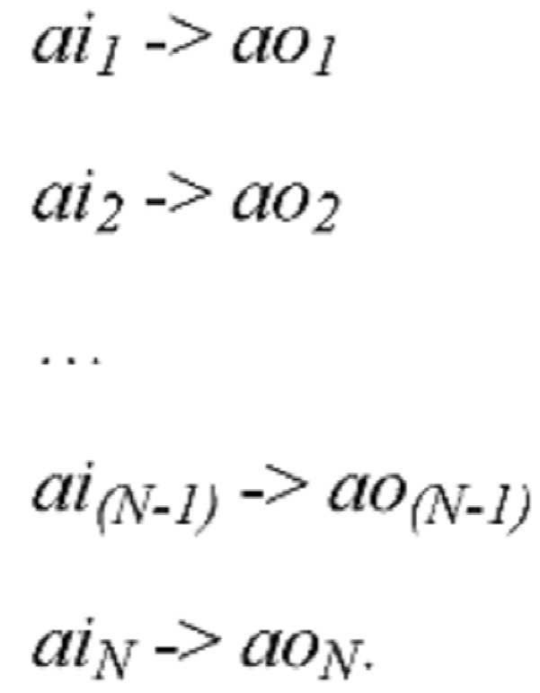
다음 주기에, T<t<2T,In the next cycle, T<t<2T ,

다음 주기 동안, 2T<t<3T:During the next cycle, 2T<t<3T :
![]()
![]()

구체적으로, 각 주기 동안 하나의 입력 어드레스만이 그 다음 출력 어드레스로의 맵핑을 순차적으로 변경한다. N 주기 다음, 모든 입력 어드레스는 맵핑을 그 다음 출력 어드레스로 변경한다. M>N이기 때문에, 이러한 어드레스 순환이 작동하도록 "빈(empty)" 공간 (또는 "갭(gaps)")이 있다. 간단한 설명예에서, 입력 어드레스 ai k 는 충분한 시간 주기가 주어지면 ao 1 , ao 2 ,..., ao M 중 하나에 맵핑될 수 있음이 자명하다.Specifically, during each period, only one input address sequentially changes the mapping to the next output address. After N periods, all input addresses change the mapping to the next output address. Since M>N, there is a "empty" space (or "gaps") for this address cycle to work. In a simple illustrative example, it is obvious that the input address ai k can be mapped to one of ao 1 , ao 2 ,..., ao M given a sufficient time period.
상기의 예는 정확한 웨어 레벨링을 도시한다. 입력 어드레스가 응용 프로그램이 쓰려고 하는 논리 어드레스라면, 어드레스 순환을 통해 동일한 논리 어드레스가 SCM 작동에 사용된 물리적 어드레스인 상이한 출력 어드레스에 맵핑된다. 쓰기가 하나의 특정 논리 어드레스에 집중되는 경우 어드레스 순환 체계는 웨어 레벨링하기 위해 M개의 물리적 어드레스로 쓰기를 재분배 하는데 도움이 될 수 있다. 어드레스 순환은 또한 구현이 비교적 쉽고, 그리고 맵핑 테이블을 구성할 필요가 없다.The above example shows correct wear leveling. If the input address is a logical address that the application program intends to write, the same logical address is mapped to a different output address, which is the physical address used for SCM operation through address cycling. If writes are concentrated on one specific logical address, the address rotation scheme can help redistribute writes to M physical addresses for wear leveling. Address rotation is also relatively easy to implement, and there is no need to construct a mapping table.
Qureshi 2009인 참조문헌은 주기인 T 자체가 동적임을 제안한다. ai k 가 해당 주기 동안 다시 맵핑될 입력 어드레스인 경우, ai k 에 대한 특정 수의 쓰기가 발생한 후 다시 맵핑이 이루어지도록 제안한다. 이러한 제안은 얼마나 많은 쓰기가 발생했는지와 쓰기 작업이 어디에 쓰여 있는지에 대한 많은 부기(bookkeeping)를 필요로 한다. 그러나 사실 많은 쓰기가 ai k 와 상이한 어드레스에서 발생하더라도, 웨어 레벨링의 필요성은 다르지 않지만, 유일하게 이동 가능한 맵핑은 여전히 ai k 이다. 따라서, 본 명세서에서는 주의 깊게 선택된 고정된 시간 주기인 T가 양호해야 하고, 부기를 최소화한다고 가정한다.The Qureshi 2009 reference suggests that the period T itself is dynamic. If ai k is an input address to be remapped during the corresponding period, it is proposed to perform re-mapping after a specific number of writes to ai k occur. These proposals require a lot of bookkeeping on how many writes have occurred and where the writes are being written. However, although in fact many writes occur at addresses different from ai k , the need for wear leveling is not different, but the only movable mapping is still ai k . Therefore, in this specification, it is assumed that T, which is a carefully selected fixed time period, should be good and that bookkeeping is minimized.
Qureshi 2009인 참조문헌는 "그룹 어드레스 순환(group address rotation)" 개념을 고려하지 않는다. 어드레스 순환은 개별 어드레스에 적용될 수 있으나, 웨어 레벨링 성능의 손실없이 구현을 단순화하기 위해, 본 발명의 일 실시예에 따라 다수의 어드레스가 그룹화되고 함께 순환한다. 즉, 어드레스 순환은 어드레스의 최상위 비트(most-significant-bits, MSBs)에서 작동해야 한다. 예를 들어, 관심있는 전체 어드레스 공간이 64개의 그룹으로 분할된 경우, 어드레스 순환 계산에 6 MSB 비트만이 필요하다.The Qureshi 2009 reference does not take into account the concept of "group address rotation". Address rotation can be applied to individual addresses, but in order to simplify implementation without loss of wear leveling performance, a plurality of addresses are grouped and cycled together according to an embodiment of the present invention. That is, address cycling must operate on the most-significant-bits (MSBs) of the address. For example, if the entire address space of interest is divided into 64 groups, only 6 MSB bits are required to calculate the address rotation.
특히 고정 시간 주기 및 그룹 어드레스 순환의 개선으로의 어드레스 순환은, 구현이 간단하지만 단기 웨어 레벨링 효과가 아닌 장기 웨어 레벨링 효과만을 가져온다. N개의 시간 주기에서 각 어드레스는 (N-1)시간 간격 또는 (N-1)*T 시간 이상 고정적이다. 따라서 응용 프로그램이 (N-1)*T시간 동안 특정 어드레스에 반복적으로 쓰기를 원한다면, 어드레스 순환 방식은 웨어 레벨링에 도움이 되지 않는다. (N-1)*T 보다 오래 지속되는 경우에만 반복 쓰기에 도움이 된다. 이제 N은 많은 수의 대안 중 어드레스가 순환되도록 허용하기 위해 설계되었지만, T는 쓰기 성능 부담을 너무 많이 줄일 수 없다. 따라서 (N-1)*T는 어드레스 순환이 효과적이지 않은 적은 양의 시간이 아닐 수 있다.In particular, the address circulation due to the improvement of the fixed time period and the group address circulation is simple to implement, but only brings about a long-term wear leveling effect, not a short-term wear leveling effect. In N time periods, each address is fixed over (N-1) time interval or (N-1)* T time. So, if an application program wants to repeatedly write to a specific address for (N-1)*T times, the address rotation method does not help with wear leveling. (N-1)* Helps repetitive writing only if it lasts longer than T. Now N is designed to allow addresses to be cycled among a large number of alternatives, but T cannot reduce the write performance burden too much. Therefore, (N-1)*T may not be a small amount of time for which address cycling is not effective.
웨어 레벨링 내구성의 성능을 향상시키기 위해, 본 발명은 어드레스 순환과 접합하여 사용될 수 있는 캐시 필터링(cache filtering)이라고 불리는 새로운 웨어 레벨링 방식을 개시한다. 캐시 필터링은 어드레스 순환 방식이 아닌, 단기 웨어 레벨링에 효과적이다. 그러므로 캐시 필터링과 어드레스 순환은 좋은 조합이다. In order to improve the performance of wear leveling durability, the present invention discloses a new wear leveling method called cache filtering that can be used in conjunction with address circulation. Cache filtering is effective for short-term wear leveling, not for address rotation. Therefore, cache filtering and address rotation are a good combination.
기본적인 읽기 및 쓰기 캐시 설계의 간략한 요약이 다음과 같이 설명된다. 캐시는 대개 메인 메모리 유닛에 비해 빠르지만 작으며, 메인 메모리 유닛에 내용의 하위 집합을 저장한다. 달리 특정되지 않으면 본 명세서 전반에, 논의 중인 메인 메모리 유닛은 SCM인 것으로 가정된다. 캐시가 어드레싱 패턴이 지역성을 가져서 유용하기 때문에 - 이전에 엑세스한 어드레스를 읽기 또는 쓰기할 가능성이 크다. 읽기 작업에서 최근에 읽기한 내용이 캐시에 복사되고 다시 읽기되면, 성능을 얻도록 캐시에서 읽어질 수 있다. 쓰기 작업에서 최근에 쓰기된 내용은 먼저 메인 메모리 유닛 대신 캐시에 쓰기된다. 동일한 위치에 새로운 쓰기가 다시 발생하면 캐시에 쓰기되어 일부 쓰기 작업이 메인 메모리 유닛에 저장 될 수 있다. 통상적으로 읽기 및 쓰기 캐시는 하나의 캐시로서 구현되며, 여기서 캐시 엔트리가 메인 메모리 대응과 상이한지(즉, 보다 새로운 것인지) 여부를 나타내기 위해 각 캐시 엔트리에 "더티(dirty)" 비트가 존재한다.A brief summary of the basic read and write cache design is described as follows. The cache is usually faster but smaller than the main memory unit, and stores a subset of its contents in the main memory unit. Throughout this specification, unless otherwise specified, it is assumed that the main memory unit under discussion is an SCM. Since the cache is useful because the addressing pattern is local-it is likely to read or write previously accessed addresses. In a read operation, when the most recently read content is copied to the cache and read again, it can be read from the cache to gain performance. In a write operation, the most recently written content is first written to the cache instead of the main memory unit. When a new write occurs in the same location again, it is written to the cache and some write operations can be stored in the main memory unit. Typically read and write caches are implemented as one cache, where there is a "dirty" bit in each cache entry to indicate whether the cache entry is different from its main memory counterpart (i.e. newer). .
캐시 필터링 방식에서, 읽기 캐시 부분은 통상의 읽기 캐시와 동일하다. 그러나 쓰기 부분은 상이하다. 일반적으로, 캐시 작업에 대한 쓰기는 메인 메모리에 쓰기하지 않고 캐시에 쓰기할 것이다. 캐시 필터링 방식에서, 쓰기 작업 동안, 캐시 히트가 발생하면, 쓰기 작업은 캐시에 쓰기하고 예정된 어드레스 위치로부터 메인 메모리의 상이한(different) 위치에 쓰기할 것이다. 캐시 엔트리 내용이 예정된 어드레스 위치의 내용과 다르므로(즉, 보다 새로운 것이므로), 캐시 엔트리의 더티 비트가 설정될 것이다. 쓰기 캐시 미스에 대한 두 가지 경우가 있다. 첫째 경우에는 쓰기 캐시가 가득 차지 않은 경우 쓰기 캐시뿐만 아니라 예정된 어드레스 위치의 메인 메모리 유닛에 새로운 엔트리가 쓰기되는 경우이다. 다른 경우는 캐시가 가득찬 경우(그리고 어떤 엔트리도 제거될 수 없는 경우) 새로운 엔트리는 쓰기 캐시가 아닌 예정된 어드레스 위치의 메인 메모리 유닛에만 쓰기되는 경우이다. In the cache filtering method, the read cache portion is the same as the normal read cache. However, the writing part is different. In general, writes to cache operations will write to the cache instead of writing to main memory. When the cache filtering method, for a write operation, a cache hit occurs, the write operation will be writing to different (different) location of the main memory from a write to a predetermined address location in the cache. Since the contents of the cache entry are different from the contents of the predetermined address location (i.e., because they are newer), the dirty bit of the cache entry will be set. There are two cases for write cache misses. In the first case, when the write cache is not full, a new entry is written not only to the write cache but also to the main memory unit at a predetermined address position. The other case is when the cache is full (and no entries can be removed), and new entries are only written to the main memory unit at the intended address location, not to the write cache.
본 발명에서, 이러한 경우와 달리, 상이한 쓰기 캐시 미스를 처리하기 위한 대안적인 방법을 포함한다. 쓰기 작업 동안, 쓰기 캐시 미스가 발생하면 쓰기 작업은 캐시에 쓰기되고 또한 예정된 어드레스 위치에서 메인 메모리의 상이한 위치에 작성된다. 이제 캐시 엔트리가 예정된 어드레스 위치의 내용과 다르므로(즉, 보다 새로운 것이므로), 캐시 엔트리의 더티 비트가 설정된다. 캐시에서 쓰기 캐시가 가득차면, 기존에 존재하던 쓰기 캐시 엔트리 중 하나가 쓰기 캐시에서 제거되어 현재 들어오는 쓰기 데이터를 위한 자리를 만든다. 쓰기 캐시가 가득찬 경우 제거할 쓰기 캐시 엔트리를 선택하는 다수의 방법이 존재할 수 있는데, 본 발명에서는 특별한 제거 방법이 특정되지 않는다. 제거된 엔트리는 더티(dirty)일 수 있고, 예정된 어드레스 위치로 플러싱될 필요가 있음에 유의해야 한다. In the present invention, unlike this case, an alternative method for handling different write cache misses is included. During a write operation, if a write cache miss occurs, the write operation is written to the cache and also written to a different location in the main memory at a predetermined address location. Now that the cache entry is different from the contents of the intended address location (ie, it is newer), the dirty bit of the cache entry is set. When the write cache is full in the cache, one of the existing write cache entries is removed from the write cache to make room for the currently incoming write data. There may be a number of methods for selecting a write cache entry to be removed when the write cache is full, but no special removal method is specified in the present invention. It should be noted that the removed entry can be dirty and needs to be flushed to its intended address location.
캐시 필터링 개념에서 쓰기 캐시의 목적은 최근에 쓰기된 어드레스를 감지하고 필터링하는 것이다. 따라서, 웨어 레벨링의 목적을 위해 해당 내용은 예정된 어드레스와 상이한 임시 메모리 위치에 로깅될 수 있다. 그러나 이러한 로깅 쓰기에 사용할 임시 메모리 공간의 위치와 관련하여 문제가 있다. 어드레스 순환에서 M>N이며, 현재 맵핑되지 않은 메모리 공간이 있음을 상기해야 한다. 이러한 로깅 쓰기는 사용되지 않은 메모리 공간 중 하나에 쓰기되어야 한다. 어드레스 순환과 함께, 로깅 쓰기에 사용되는 메모리 공간은 시간 경과에 따라 더 순환한다.In the concept of cache filtering, the purpose of the write cache is to detect and filter recently written addresses. Thus, for the purpose of wear leveling, the content may be logged in a temporary memory location different from the predetermined address. However, there is a problem with the location of the temporary memory space to be used for these logging writes. It should be recalled that in the address cycle, M>N, and there is currently an unmapped memory space. These logging writes must be written to one of the unused memory spaces. Along with the address cycle, the memory space used for logging writes cycles more over time.
캐시 엔트리는 잠시 동안 엑세스 되지 않으면 제거될 것이다. 언제 어떠한 엔트리를 제거할지 결정하는 선택 가능한 많은 기술이 있다. 쓰기 캐시 엔트리는 폐기(retired)되고 더티 비트가 설정된 경우에만 예정된 어드레스 위치로 플러싱된다. 쓰기 캐시 엔트리가 예정된 어드레스 위치로 플러싱 되기 이전에 갑작스런 전력 손실이 발생하면, 휘발성 쓰기 캐시의 내용이 손실되더라도 비휘발성 임시 위치의 내용이 사용되어 예정된 어드레스 위치로 정확한 내용을 복원할 수 있다.Cache entries will be removed if they are not accessed for a while. There are many techniques to choose from for deciding when to remove which entries. Write cache entries are retired and are flushed to their intended address location only if the dirty bit is set. If a sudden power loss occurs before the write cache entry is flushed to a predetermined address location, even if the contents of the volatile write cache are lost, the contents of the non-volatile temporary location can be used to restore the correct contents to the predetermined address location.
아키텍쳐적 선택이 어떻게 동일한 메모리 어드레스에 K회 반복 쓰기를 처리하는지에 대해 검토하고 비교해본다. 아키텍쳐적 선택은 (1) 쓰기 캐시 없이, (2) 전통적 쓰기 캐시와 함께 그리고 (3) 캐시 필터링에 해당한다. 캐시가 없는 메모리 시스템의 경우 이러한 K회 쓰기가 (N-1)*T 이내에 발생하면 예정된 어드레스 위치는 K회 쓰기의 영향을 받는다. 전통적인 쓰기 캐시를 갖는 메모리 시스템의 경우, 쓰기 캐시는 대부분의 쓰기를 흡수하고 예정된 어드레스 위치는 훨씬 적은 횟수로 쓰기된다. 쓰기 캐시가 휘발성이므로, 갑작스러운 전력 손실이 발생하면 쓰기 캐시의 내용은 손실된다. 전력이 손실되기 전 쓰기 캐시 엔트리의 일부가 더티인 경우 이것은 치명적이다. 모든 더티 쓰기 캐시 엔트리가 플러싱될 때까지 호스트가 정지되면 성능에 큰 영향을 미친다. 캐시 필터링을 갖는 메모리 시스템의 경우 메모리 하위 시스템은 K+1회 쓰기되지만, 예정된 어드레스 위치에는 한번만 쓰기된다. 3개의 아키텍쳐적 선택 중에서, 캐시 필터링만이 웨어를 레벨링시킬 수 있으며 갑작스러운 전력 손실에 영향을 받지 않는다. Consider and compare how the architectural choice handles K repeated writes to the same memory address. The architectural choices correspond to (1) without write cache, (2) with traditional write cache and (3) cache filtering. In the case of a memory system without a cache, if these K writes occur within (N-1)*T , the predetermined address position is affected by K writes. In the case of a memory system with a traditional write cache, the write cache absorbs most of the writes and the intended address location is written much less frequently. Since the write cache is volatile, the contents of the write cache are lost if a sudden power loss occurs. This is fatal if some of the write cache entries are dirty before power is lost. If the host hangs until all dirty write cache entries have been flushed, it will have a major impact on performance. In the case of a memory system with cache filtering, the memory subsystem is written K+1 times, but only once to a predetermined address location. Of the three architectural choices, only cache filtering can level the wear and is not affected by sudden power losses.
어드레스 순환 및 캐시 필터링을 결합하는 웨어 레벨링 아키텍쳐(wear leveling architecture)를 구축하는 방법은 다음과 같이 개시된다. 일반성(generality)의 손실 없이, 일반적인 SCM의 특성이 웨어 레벨링 설계의 예를 설명하기 위해 기술된다.A method of constructing a wear leveling architecture that combines address rotation and cache filtering is disclosed as follows. Without loss of generality, the characteristics of a general SCM are described to illustrate an example of a wear leveling design.
SCM 메모리 시스템의 전체 용량은 (D+E)*C (바이트 단위로 측정됨)에 따라 결정될 수 있으며, 여기서 C는 각각의 SCM칩의 용량이다. D칩은 데이터부를 저장하기 위해 사용되며, 그리고 E칩은 오류-정정 코드(ECC) 체크 바이트부를 위해 사용되며 그리고 일부 메타데이터는 데이터 관리를 위해 사용된다. 각각의 SCM칩은 z-비트 데이터 폭을 갖는 I/O 데이터와 용량에 따라 적절한 크기의 어드레스 비트를 갖는다. 각각의 SCM은 DDR(double-data-rate) 신호를 갖는, 최대 U(MHz 단위로 측정됨)로 클럭될 수 있다. 다시 말해, 각각의 클럭 사이클마다, 2*z 비트는 각각의 SCM 칩을 사용할 수 있다. SCM칩은 t R 의 읽기 지연속도(latency) 및 t W 의 쓰기 지연속도를 갖는다(둘다 10억분의 1초 단위로 측정됨). 또한, SCM칩은 P 파티션을 갖고 그리고 상기 파티션은 독립적이고 병렬적으로 읽기 및 쓸수있다고 가정한다. The total capacity of the SCM memory system can be determined according to (D+E)*C (measured in bytes), where C is the capacity of each SCM chip. The D chip is used to store the data portion, and the E chip is used for the Error-Correcting Code (ECC) check byte portion, and some metadata is used for data management. Each SCM chip has I/O data having a z-bit data width and an address bit of an appropriate size according to its capacity. Each SCM can be clocked with a maximum U (measured in MHz) with a double-data-rate (DDR) signal. In other words, for each clock cycle, 2*z bits can use each SCM chip. The SCM chip has a read latency of t R and a write latency of t W (both measured in units of one billionth of a second). In addition, it is assumed that the SCM chip has a P partition and that the partition can be read and written independently and in parallel.
이러한 관점에서 보면, SCM의 t R 과 t W 은 DRAM의 것보다 더 크며, NAND 플래쉬의 것보다는 더 작다. 병렬 파티션을 사용하면, SCM은 DRAM에 비해 일부 성능을 복구할 수 있다. 이것은 SCM의 I/O 대역폭 (U 및 z로 결정됨)이 t R 또는 t W 보다, DRAM의 그것에 더 가깝기 때문이다. 각각의 읽기/쓰기 작업이 완료되는데 오래 걸리는 경우에도, 다수의 읽기/쓰기 작업을 병렬로 시작하는 것은 I/O를 채우기 위해 효과적인 방법인 바, 이로써 성능 차이를 줄인다. From this point of view, t R and t W of SCM are larger than those of DRAM and smaller than those of NAND flash. Using parallel partitions, SCM can recover some performance compared to DRAM. This is because the SCM's I/O bandwidth (determined by U and z) is closer to that of the DRAM than t R or t W. Even if each read/write operation takes a long time to complete, starting multiple read/write operations in parallel is an effective way to fill I/O, thereby reducing the performance gap.
D SCM칩 및 대응하는 E SCM칩의 일부는 동일한 어드레스 비트를 공유할 수 있다. SCM칩의 이러한 그룹을 영역(region)이라고 명명한다. 예를 들어, 8개의 D칩 및 1개의 E 칩이 동일한 어드레스를 공유하고, 그리고 C는 16 기가바이트인 경우, 이 때의 영역의 크기는 128 기가바이트이다. 8개의 D칩 및 1개의 E칩이 동일한 어드레스를 공유하고 z=8인 경우, 각각의 사이클에서, 사용 가능한 데이터는 (8+1)*8*2 비트=18 바이트이다. 도 1은 동일한 비휘발성 메모리칩 내의 데이터 그룹과 연관된 오류 정정 코드(ECC) 체크 바이트 및 메타데이터의 저장을 공유하도록 비휘발성 메모리 칩을 구성하는 예를 도시한다. 총 9개의 칩이 SCM의 영역을 위해 사용되며, 여기서 8개의 칩(칩 1 내지 8)은 데이터를 저장하기 위해 사용되며 그리고 1개의 칩(칩 9)는 ECC 데이터 및 메타데이터를 저장하기 위해 사용된다. 화살표가 가리키는 위치에 도시된 각각의 어드레스 위치에 대해, 데이터는 첫번재 8개의 칩에 저장된다. ECC부 및 메타데이터는 칩 9에 저장된다. The D SCM chip and some of the corresponding E SCM chips may share the same address bits. This group of SCM chips is called a region. For example, when 8 D chips and 1 E chip share the same address, and C is 16 gigabytes, the size of the area at this time is 128 gigabytes. When 8 D chips and 1 E chip share the same address and z=8, in each cycle, the usable data is (8+1)*8*2 bits=18 bytes. 1 shows an example of configuring a nonvolatile memory chip to share storage of error correction code (ECC) check bytes and metadata associated with a group of data in the same nonvolatile memory chip. A total of 9 chips are used for the area of the SCM, where 8 chips (chips 1 to 8) are used to store data and 1 chip (chip 9) is used to store ECC data and metadata. do. For each address position shown at the position indicated by the arrow, data is stored in the first eight chips. The ECC unit and metadata are stored in chip 9.
실제로, 메인 메모리에 대한 최소 액세스 유닛은 적어도 64바이트이다. 128바이트의 최소 액세스 유닛을 갖는 메인 메모리를 설계한다고 가정하면, 각각의 메모리 액세스는, 128바이트가 데이터이다. 총 144바이트를 제공하기 위해 8개의 연속 사이클을 볼 수 있어서 이것의 중요성은 두 가지이다. 첫째, "더 큰(bigger)"ECC 블록(128 데이터 바이트)이 더 나은 오류 정정 성능을 위해 SCM에 사용될 수 있다. 이것은 전통적으로 높은 디코더 지연 때문에 DRAM에 사용되지 않는다. 그러나, SCM의 경우, t R 이 크기 때문에, 디코더 지연이 더 클수록 영향은 훨씬 더 적다. 둘째, E칩으로부터의 데이터가 블록으로 구성될 때, 웨어 레벨링을 위한 일부 메타데이터를 넣을 자리가 더 많다. 이러한 요인은 아마도 우리의 논의를 위해 더욱 중요하다. In fact, the minimum access unit to the main memory is at least 64 bytes. Assuming that a main memory with a minimum access unit of 128 bytes is designed, each memory access is 128 bytes of data. We can see eight consecutive cycles to give a total of 144 bytes, so the importance of this is twofold. First, a "bigger" ECC block (128 data bytes) can be used in the SCM for better error correction performance. It is traditionally not used in DRAM due to the high decoder latency. However, in the case of SCM, since t R is large, the larger the decoder delay, the smaller the impact. Second, when the data from the E chip is composed of blocks, there are more places to put some metadata for wear leveling. These factors are perhaps even more important for our discussion.
전체 SCM 메모리 시스템은 다수의 영역으로 분할될 수 있다. 각각의 영역은 어드레스 순환을 위한 베이식 유닛이다. 각각의 영역의 어드레스 공간은 M개의 그룹으로 더 분할된다. 영역의 대부분의 그룹은 2가지 유형의 그룹인 쉐도우(shadow) 그룹 및 로깅(logging) 그룹을 제외하고, 데이터를 저장하기 위해 사용되어, 데이터 그룹으로 지칭된다. 쉐도우 그룹 및 로깅 그룹은 함께 중복 그룹이라 불리는데, 이들은 웨어 레벨링을 위한 메모리 오버헤드(memory overhead)이기 때문이다. 로깅 그룹의 적절한 개수가 메모리 시스템을 위해 선택될 수 있다. 예를 들어, 128 기가바이트 영역이 1개의 쉐도우 그룹 및 2개의 로깅 그룹을 갖는 64개의 그룹으로 분할된 경우, 단지 122 기가바이트의 메모리 공간만이 데이터를 저장하는데 사용될 수 있다. The entire SCM memory system can be divided into multiple areas. Each area is a basic unit for address circulation. The address space of each region is further divided into M groups. Most of the group two types of groups of the shadow (shadow) group, and logging of an area except for the (logging) group, and is used to store data, and is referred to as a data group. Together, the shadow group and the logging group are called redundant groups because they are memory overhead for wear leveling. An appropriate number of logging groups can be selected for the memory system. For example, if a 128 gigabyte area is divided into 64 groups with 1 shadow group and 2 logging groups, only 122 gigabytes of memory space can be used to store data.
임의의 주어진 시간에, 선셋 그룹이라 불리는 데이터 그룹의 하나의 컨텐츠를 쉐도우 그룹에 복사하는 배경 프로세스가 있다. 이러한 복사 프로세스의 시간 주기는 T이다. T는 이러한 배경 복사(쓰기) 프로세스가 쓰기 대역폭의 작은 부분(예로, 1-2% 보다 작게)만을 취하도록 설계된다. 시간 T가 경과하면, 쉐도우 그룹은 이전 선셋 그룹의 식별자를 취하며 그리고 데이터 그룹의 하나가 된다. 선셋 그룹은 중복 그룹에 합쳐진다(join). 중복 그룹 사이에서 순환하기 위해, 선셋 그룹은 로깅 그룹의 하나로 합쳐지고, 그리고 로깅 그룹의 하나는 새로운 쉐도우 그룹의 위치 등을 취한다. 이러한 방식으로, 모든 그룹은 M*N*T 시간 이후에 데이터 그룹, 로깅 그룹 및 쉐도우 그룹 사이에서 그들의 역할을 순환한다. At any given time, there is a background process that copies the contents of one data group called a sunset group into a shadow group. The time period of this copying process is T. T is designed such that this background copy (write) process only takes a small portion of the write bandwidth (eg, less than 1-2%). When time T elapses, the shadow group takes the identifier of the previous sunset group and becomes one of the data groups. The sunset group is joined into a redundant group. To cycle between redundant groups, the sunset group is merged into one of the logging groups, and one of the logging groups takes the location of a new shadow group, and so on. In this way, all groups cycle their roles between data groups, logging groups and shadow groups after M*N*T times.
그룹 유형을 구별하는 방법은 SCM에서 메타데이터의 일부로 저장된 그룹 라벨(label)에 의한다. 다음의 예는 그들의 변경되는 유형을 반영하기 위해 시간에 따라 그룹 라벨이 어떻게 변경되는지 도시한다. 여기의 예에서, M=64 이다. To distinguish between the type of group is by labeling group (label) is stored as part of the metadata in the SCM. The following example shows how group labels change over time to reflect their changing type. In the example here, M=64.

여기의 예에서, 그룹 라벨 0은 선셋 그룹이며, 그리고 그룹 라벨 61은 쉐도우 그룹이고, 그룹 라벨 62, 63은 각각 로깅 그룹이다. 이 시간 동안, 입력 어드레스는 입력 어드레스 0 내지 60에 대한 출력 어드레스와 동일하다. In the example here, group label 0 is a sunset group, group label 61 is a shadow group, and group labels 62 and 63 are logging groups, respectively. During this time, the input address is the same as the output address for input addresses 0 to 60.
시간 T가 경과하면, 그룹 라벨 64는 다음의 그룹 라벨을 생산하기 위해, 0으로 라벨되도록 사용되는 그룹에 쓰기될 것이다: After time T has elapsed, the group label 64 will be written to the group used to be labeled as 0, to produce the following group label:

이제 그룹 라벨 1은 선셋 그룹이 되고, 그룹 62는 쉐도우 그룹이 되며, 그룹 63, 64는 로깅 그룹이 된다. 이제 그룹 61은 데이터 그룹이 된다. 현재 시간 주기에서, 입력 어드레스 0은 출력 어드레스 61에 맵핑되는 동시에, 입력 어드레스는 어드레스 1부터 60까지 출력 어드레스와 동일하다. Now group label 1 becomes the sunset group, group 62 becomes the shadow group, and groups 63 and 64 become the logging group. Group 61 is now a data group. In the current time period, the input address 0 is mapped to the output address 61, while the input address is the same as the output address from addresses 1 to 60.
유사하게, 다음 시간 주기에서 상태는 다음과 같이 도시되며, 그리고 어드레스 순환 프로세스는 계속된다. Similarly, in the next time period the state is shown as follows, and the address cycle process continues.

이러한 설계를 주목하면, 그룹 라벨은 항상 64개의 연속 번호가 될 것이다. 이러한 라벨을 저장하기 위해 8bit를 사용할 경우, 그들은 모듈로-256 센스(즉, ..., 254, 255, 0, 1, ... 연속으로 간주됨)에서 연속될 것이다. 가장 작은 그룹 라벨은 항상 선셋 그룹일 것이며, 동시에 3개의 가장 큰 그룹 라벨은 중복 그룹일 것이다. 이들의 크기의 비교는 또한 모듈로-256 센스이며, 그러므로 0은 255보다 1이 더 크다. 언제든지 64개의 연속 번호가 있을 수 있으므로, 혼동은 없을 것이다. 임의의 주어진 시간의 인스턴스에서, 64개의 연속하는 그룹 라벨은 어드레스 순환 - 각각의 그룹의 그룹 유형의 상태 및 입력과 출력 어드레스 맵핑이 어떻게 되어야되는지를 추론하기 위해 사용될 수 있다. Taking note of this design, the group label will always be 64 consecutive numbers. If you use 8 bits to store these labels, they will be contiguous in the modulo-256 sense (ie ..., 254, 255, 0, 1, ... are considered continuous). The smallest group label will always be the sunset group, and at the same time the 3 largest group labels will be the duplicate group. The comparison of their size is also modulo-256 sense, so 0 is 1 greater than 255. There can be 64 consecutive numbers at any time, so there will be no confusion. At any given time instance, 64 consecutive group labels can be used to deduce the address cycle-the state of each group's group type and what the input and output address mapping should be.
상기에 도시된 특정한 예시에서는 그룹 라벨이 변화하는 유형을 반영하도록 시간에 따라 변화하는 것을 설명한다. 이러한 예시는 본 발명의 제한되어 해석되어서는 안된다. In the specific example shown above, it is described that the group label changes over time to reflect the changing type. These examples are not intended to be construed as being limited to the present invention.
이러한 그룹 라벨이 SCM 내에 저장됨에 따라, 전력이 손실된 이후에도, 시스템은 이러한 그룹 라벨에 의해 어드레스 순환의 상태를 복원할 수 있다. 선셋 그룹으로부터 쉐도우 그룹으로의 배경 복사의 정확한 상태를 알 수는 없어도, 전력 손실 이후에, 시간 주기 T를 재시작할 수 있고, 그리고 그룹의 시작부터 배경 복사를 재실행할 수 있다. As these group labels are stored in the SCM, even after power is lost, the system can restore the state of address circulation by means of these group labels. Although the exact status of the background copy from the sunset group to the shadow group is not known, after power loss, the time period T can be restarted, and the background copy can be re-run from the beginning of the group.
ECC 데이터 및 메타데이터에 대한 공유된 저장의 경우, ECC 데이터는 모든 유형의 메모리 그룹에 대해 비휘발성 메모리의 ECC부 내에 항상 저장된다. 대응하는 메모리 그룹에 대한 각각의 메타데이터는 비휘발성 메모리의 메타데이터부 내에 저장된다. 각각의 데이터 그룹 또는 쉐도우 그룹에 대해, 메타데이터는 그룹 라벨만을 포함한다. 각각의 로깅 그룹에 대해, 메타데이터 그룹은 그룹 라벨, 호스트 어드레스, 호스트 어드레스와 연관된 타임스탬프를 포함한다. 도 2는 어드레스 순환에 연관된 메타데이터 구조의 예시를 도시한다. In the case of shared storage for ECC data and metadata, the ECC data is always stored in the ECC portion of the non-volatile memory for all types of memory groups. Each metadata for a corresponding memory group is stored in the metadata portion of the nonvolatile memory. For each data group or shadow group, the metadata includes only the group label. For each logging group, the metadata group includes the group label, host address, and timestamp associated with the host address. 2 shows an example of a metadata structure involved in address rotation.
로깅 그룹이 재순환되는 또다른 시간 주기인 t L 이 있다. 시간 주기인 t L 은 쓰기 캐시 크기 및 최대 쓰기 처리량에 의존한다. 최대 쓰기 처리량 및 모든 쓰기는 캐시 히트가 되도록 설계된 다음, t L 시간 동안, 이러한 쓰기는 로깅 그룹의 일부를 오버플로우하지 않도록 설계된다. 적절한 시스템 설계에서, T는 t L 보다 훨씬 더 크며 t L 의 정수배가 되어야 한다. 로깅 그룹 작동에서, 각각의 로깅 그룹은 복수의 로깅 유닛으로 분할될 수 있다. 예를 들어, 2개의 로깅 그룹은 4개의 로깅 유닛으로 더 분할된다. 각각의 로깅 유닛은 로깅 그룹의 절반이다. 쓰기 캐시 히트가 발생하면, 데이터 및 원래 입력 어드레스는 활성 로깅 유닛으로 불리는 로깅 유닛의 하나로 로그되며, 이는 다음 로깅 쓰기가 언제 쓰기될지를 결정하는 현재 포인터를 가지고 있고, 그리고 현재 포인트는 순차적으로 이동할 것이다. 별도의 쓰기 캐시 및 읽기 캐시 메모리가 사용되는 경우 쓰기 캐시 히트는 비휘발성 메모리에 쓰기될 데이터가 이미 캐시 메모리 또는 쓰기 캐시 메모리에 있음을 의미한다. 다음 tL시간 주기에서, 상이한 로깅 유닛은 활성 로깅 유닛 등이 된다. 각각의 로깅 유닛은 순서대로 활성 로깅 유닛으로써 역할을 한다. There is another time period t L during which the logging group is recycled. The time period t L depends on the write cache size and the maximum write throughput. The maximum write throughput and all writes are designed to be cache hits, and then during t L hours, these writes are designed not to overflow part of the logging group. In an appropriate system design, T is to be doubled even integer greater than L t t L. In the logging group operation, each logging group can be divided into a plurality of logging units. For example, two logging groups are further divided into four logging units. Each logging unit is half of the logging group. When a write cache hit occurs, the data and the original input address are logged into one of the logging units called the active logging unit, which has a current pointer that determines when the next logging write will be written, and the current point will move sequentially. . When separate write cache and read cache memory are used, a write cache hit means that data to be written to the nonvolatile memory is already in the cache memory or the write cache memory. In the next tL time period, the different logging units become active logging units and the like. Each logging unit in turn serves as an active logging unit.
쓰기 캐시 내부에는, 각각의 엔트리에 대해, 데이터 컨텐츠 및 입력 어드레스 외에, 유효 비트, 더티 비트, 및 타임스탬프 필드가 있다. 유효 비트는 위치가 유효 엔트리였는지 여부를 표시한다. 타임스탬프는 엔트리가 마직막으로 업데이트된 t L 시간 주기 동안을 표시한다. 타임스탬프는 매 t L 시간마다 1씩 증가하며, 이는 랩어라운드(wrap around)할 수 있다. 타임스탬프 필드를 사용하면, 어떤 쓰기 캐시 엔트리가 잠시동안 업데이트되지 않았는지 알 수 있으며, 이는 설계 파라미터에 의한 현재 타임스탬프보다 더 작은 타임스탬프 필드를 가진다. 쓰기 캐시를 검사하고 새로운 쓰기 엔트리를 위한 공간을 남겨놓기 위해 이러한 오래된 엔트리를 플러쉬하는 배경 프로세스가 있다. 플러쉬 쓰기는 예정된 어드레스 위치에 쓰기될 것이다. Inside the write cache, for each entry, in addition to the data content and input address, there are valid bit, dirty bit, and timestamp fields. The valid bit indicates whether the position was a valid entry. The timestamp indicates during the t L time period the entry was last updated. The timestamp increases by 1 every t L hours, which can wrap around. Using the timestamp field, you can see which write cache entry has not been updated for a while, which has a smaller timestamp field than the current timestamp by design parameters. There is a background process that checks the write cache and flushes these old entries to make room for new write entries. The flush write will be written to the intended address location.
로깅 유닛 각각은 순서대로 활성 로깅 유닛의 역할을 취하는 바, 로깅 쓰기가 이전에 로그된 것을 덮어쓰는 것을 방지하는 방법에 관한 문제가 있었다. 특정 엔트리가 이전의 로깅 쓰기 이후에 업데이트를 보았을 경우, 종래의 로깅 쓰기는 삭제할 수 있다. 특정 엔트리가 이전의 로깅 쓰기 이후에 업데이트를 보지 못한 경우, 엔트리는 쓰기 캐시에 종래의 타임스탬프를 가져야하며, 그리고 플러쉬될 것이다. 이것이 로깅 그룹을 재활용하고 로깅을 계속할 수 있는 이유이다. Since each logging unit in turn takes the role of an active logging unit, there is a problem with how to prevent logging writes from overwriting previously logged ones. If a particular entry sees an update after the previous logging write, the conventional logging write can be deleted. If a particular entry has not seen an update since the previous logging write, the entry should have a conventional timestamp in the write cache, and will be flushed. This is why you can recycle the logging group and continue logging.
로깅 그룹이 로깅 쓰기를 수행할 때, 이것은 또한 타임스탬프를 메타데이터로 저장한다. 타임스탬프 필드는 SCM 제어기에 의해 로깅 유닛의 상태를 결정하도록 사용되며, 이는 그룹 라벨이 어드레스 순환의 상태를 결정하기 위해 사용되는 방법과 유사하다. 복수의 로깅 유닛이 있기 때문에, 그들은 랩핑할 때까지 증가하는 타임스탬프 필드를 취할 것이다. 가장 큰 타임스탬프(또한 모듈로 센스)를 갖는 로깅 유닛은 현재 활성 로깅 유닛이다. 전력 손실이 발생할 때, 로깅 유닛의 타임스탬프 필드를 검사함으로써 전력 손실 이전에 어떤 로깅 유닛이 활성 로깅 유닛인지 결정할 수 있다. 이로부터 로깅 유닛의 데이터가 복원이 필요한지, 그리고 어떤 로깅 유닛의 데이터를 무시할 수 있는지 결정할 수 있다. 도 2에 도시된 바와 같이, 로깅 쓰기에 사용되지 않는 하나의 특정 위치(가장 낮은 어드레스 위치라 함)를 예비할 경우, 그룹 라벨에 대한 동일한 필드 및 타임스탬프를 사용할 수 있으며, 그리고 메타데이터의 너무 많은 공간을 차지하지 않는다. When a logging group performs a logging write, it also stores a timestamp as metadata. The timestamp field is used by the SCM controller to determine the state of the logging unit, which is similar to how the group label is used to determine the state of the address cycle. Since there are multiple logging units, they will take an incremental timestamp field until wrapping. The logging unit with the largest timestamp (also modulo sense) is the currently active logging unit. When power loss occurs, it is possible to determine which logging unit is the active logging unit prior to power loss by examining the timestamp field of the logging unit. From this, it is possible to determine whether the data of the logging unit needs to be restored, and whether the data of the logging unit can be ignored. As shown in Fig. 2, if you reserve one specific location (referred to as the lowest address location) that is not used for logging writes, you can use the same field and timestamp for the group label, and too much of the metadata. It doesn't take up much space.
도 3은 SCM 웨어 레벨링 아키텍쳐(100)의 블록 다이아그램을 도시한다. 호스트 측에서, 인터페이스 신호는 호스트 어드레스, 호스트 읽기 데이터 및 호스트 쓰기 데이터를 포함한다. SCM 측에서, 인터페이스 신호는 SCM 어드레스, SCM 읽기 데이터 및 SCM 쓰기 데이터를 포함한다. 본 발명의 실시예를 통합한 시스템은 어드레스 순환 유닛(310), 배경 복사 유닛(320), 캐시 유닛(330), 타이밍 제어 유닛(350) 및 SCM 메모리 제어기 유닛(340)을 포함할 수 있다. 그럼에도, 본 발명의 실시예는 어드레스 순환을 제외할 수 있다. 어드레스 순환 유닛(310)은 입력(호스트) 어드레스 및 출력(SCM) 어드레스 맵핑을 결정한다. 배경 복사 유닛(320)은 선셋 그룹에서 쉐도우 그룹으로의 복사를 수행한다. 캐시 유닛(330)은 읽기 캐시와 쓰기 캐시를 통합한다. SCM 메모리 제어기(340)는 다양한 기능적 유닛들로부터 엑세스 요구들을 수신하고 그리고 최적의 성능을 달성하기 위해 이러한 요구들의 우선 순위를 정한다(prioritizes). 타이밍 제어 유닛(350)은 시간 유닛인 T와 t L 을 관리하고, 그리고 T 시간 주기가 끝나면 어드레스 순환 유닛 및 배경 복사 유닛에 알리고, 그리고 t L 시간 주기가 끝나면 캐시 유닛에 알린다. 3 shows a block diagram of the SCM wear leveling architecture 100. On the host side, the interface signal includes a host address, host read data and host write data. On the SCM side, the interface signal includes the SCM address, SCM read data and SCM write data. A system incorporating an embodiment of the present invention may include an
읽기 작동은 상대적으로 간단하다. 호스트 어드레스는 읽기 캐시에 전송되며, 그리고 히트인 경우, 호스트 읽기 데이터는 읽기 캐시로부터 획득될 수 있다. 미스인 경우, 어드레스 순환 유닛은, 호스트 어드레스를 SCM 읽기를 수행하기 위해 SCM 메모리 제어기로 전송된 출력 어드레스에 맵핑할 것이다. SCM 읽기 데이터는 중복 호스트 읽기 데이터가 될 것이다. 새로운 SCM 읽기 데이터는 읽기 캐시에 들어가며, 읽기 캐시가 가득찬 경우 일부 읽기 캐시 엔트리를 대체한다. 각각의 호스트 읽기에 대해, SCM 읽기가 있을 수도 있고 아닐 수도 있다. The read operation is relatively simple. The host address is sent to the read cache, and in case of a hit, the host read data can be obtained from the read cache. In case of a miss, the address rotation unit will map the host address to the output address sent to the SCM memory controller to perform the SCM read. SCM read data will be redundant host read data. The new SCM read data goes into the read cache, and when the read cache is full, some read cache entries are replaced. For each host read, there may or may not be an SCM read.
쓰기 작동은 보다 복잡하다. 호스트 입력 어드레스는 쓰기 캐시에 전송되며, 그리고 이것이 히트인 경우, 쓰기 캐시 엔트리는 dirty=1, 새로운 타임스탬프, 및 새로운 데이터로 업데이트된다. 쓰기 캐시 히트 신호가 어드레스 순환 유닛으로 전송되면, 출력 어드레스는 활성 로깅 유닛의 현재 포인터가 될 것이며, 그리고 SCM 쓰기는 로깅 유닛에서 수행될 것이다. 로깅 쓰기에서, 호스트 어드레스는 메타데이터로써 SCM에 저장될 것이다. 이것이 미스이고, 그리고 쓰기 캐시가 가득차지 않은 경우, 쓰기 캐시 엔트리는 dirty=0, 새로운 타임스탬프 및 호스트 데이터로 생성된다. 어드레스 순환 유닛은 SCM 쓰기를 수행하기 위해 맵핑된 출력 어드레스를 생산할 것이다. 미스이지만 쓰기 캐시가 가득찬 경우, 어드레스 순환 유닛은 SCM 쓰기를 수행하기 위해 맵핑된 출력 어드레스를 생산할 것이나, 쓰기 캐시는 변경되지 않는다. 각각의 호스트 쓰기에 대해, 항상 하나의 SCM 쓰기가 있다. The write operation is more complex. The host input address is sent to the write cache, and if it is a hit, the write cache entry is updated with dirty=1, new timestamp, and new data. When the write cache hit signal is sent to the address cycle unit, the output address will be the current pointer of the active logging unit, and the SCM write will be performed in the logging unit. In logging writes, the host address will be stored in the SCM as metadata. If this is a miss, and the write cache is not full, the write cache entry is created with dirty=0, new timestamp and host data. The address cycle unit will produce mapped output addresses to perform SCM writes. If a miss, but the write cache is full, the address rotation unit will produce a mapped output address to perform the SCM write, but the write cache remains unchanged. For each host write, there is always one SCM write.
본 발명에서, 또한 상기와 상이한 쓰기 캐시 미스를 처리하기 위해 대안적인 방법을 포함한다. 미스이고 그리고 쓰기 캐시가 가득차지 않은 경우, 쓰기 캐시 엔트리는 더티 비트값이 1과 동일하고, 새로운 타임스탬프, 및 새로운 데이터로 업데이트된다. 어드레스 순환 유닛은 출력 어드레스로 활성 로깅 유닛의 현재 포인터를 생산하고, 그리고 SCM 쓰기는 로깅 유닛에서 수행될 것이다. 로깅 쓰기에서, 호스트 어드레스는 메타데이터로써 SCM에 저장될 것이다. 미스이고 그리고 쓰기 캐시가 가득찬 경우, 기존의 쓰기 캐시 엔트리 중 하나는 현재 들어오는 데이터를 위한 자리를 생성하기 위해 제거될 것이다. 쓰기 캐시 전체의 경우에서, 어떤 쓰기 캐시 엔트리를 제거할지를 선택하는 복수의 방법이 있을 수 있으며, 그리고 특정 제거 방법은 본 발명에서 명시되어 있지 않다. 제거된 엔트리는 더티(dirty)일 수 있으며, 그리고 예정 어드레스 위치로 플러쉬될 필요가 있음을 유의하여야 한다. In the present invention, it also includes an alternative method for handling write cache misses different from the above. If it is a miss and the write cache is not full, the write cache entry has a dirty bit value equal to 1, and is updated with a new timestamp and new data. The address cycle unit produces the current pointer of the active logging unit as the output address, and SCM writes will be performed in the logging unit. In logging writes, the host address will be stored in the SCM as metadata. If it is a miss and the write cache is full, one of the existing write cache entries will be removed to make room for the current incoming data. In the case of the write cache as a whole, there may be multiple ways of selecting which write cache entry to remove, and a specific removal method is not specified in the present invention. It should be noted that the removed entry can be dirty and needs to be flushed to the intended address location.
2개의 상이한 배경 쓰기 작동 및 1개의 배경 읽기 작동이 있다. 배경 복사 유닛은 선셋 그룹으로부터 읽기위해 복사 어드레스를 SCM 메모리 제어기로 전송하며, 그리고 그 때 쉐도우 그룹에 쓴다. 그러나, 호스트 쓰기가 선셋 그룹에 쓰고 있는 경우 어드레스 순환 유닛으로부터 신호를 수신한다. 그러면, 배경 복사 유닛은 어드레스가 이미 복사되었는지 여부를 검사할 필요가 있으며, 그럴 경우, 쉐도우 그룹을 새로운 데이터로 업데이트할 필요가 있다. There are two different background writing operations and one background reading operation. The background copy unit transfers the copy address to the SCM memory controller for reading from the sunset group, and then writes to the shadow group. However, when the host write is writing to the sunset group, it receives a signal from the address cycle unit. Then, the background copy unit needs to check whether the address has already been copied, and if so, it needs to update the shadow group with new data.
상이한 배경 쓰기 작동은 캐시 유닛으로부터 플러쉬 쓰기이다. 캐시 유닛은 현재 t L 시간 주기에 대응하는 타임스탬프보다 설계된 파라미터로 더 작은 타임스탬프를 갖는 임의의 엔트리를 플러쉬하기 위한 배경 프로세스를 갖는다. 플러쉬 쓰기 동안, 캐시 유닛은 쓰기 위한 맵핑된 출력 어드레스를 획득하기 위해 플러쉬 어드레스를 어드레스 순환 유닛에 전송한다. A different background write operation is a flush write from the cache unit. The cache unit has a background process for flushing any entry with a timestamp that is smaller with a designed parameter than the timestamp corresponding to the current t L time period. During a flush write, the cache unit sends the flush address to the address rotation unit to obtain a mapped output address for writing.
SCM은 읽기 또는 쓰기를 독립적으로 수행할 수 있는 P 파티션을 갖는다. 이는 SCM 메모리 제어기에 의해 작동을 병렬 처리하고 그리고 성능을 최대화하기 위해 활용될 수 있다. 읽기 및 쓰기 작동의 상이한 유형 중에서, SCM 메모리 제어기는 호스트-유도 SCM 읽기 및 쓰기 작동, 그리고 로깅 쓰기 작동과 같이, 전경(foreground) 읽기 및 쓰기 작동의 우선 순위를 정하여야 한다. 배경 복사 및 플러쉬 쓰기 작동과 같은, 배경 작동은 낮은 순위로 수행될 수 있다. SCM has a P partition that can independently perform read or write. This can be utilized by the SCM memory controller to parallelize operations and maximize performance. Among the different types of read and write operations, the SCM memory controller must prioritize foreground read and write operations, such as host-induced SCM read and write operations, and logging write operations. Background operations, such as background copy and flush write operations, may be performed with a lower priority.
도 4는 급격한 전력 손실 회복에 포함된 기능적 블록을 도시한다. 전력이 손실될 때, 캐시의 전체 컨텐츠는 손실된 것으로 간주된다. 일단 전력이 백업되면, 임베디드 프로세서(430)는 SCM을 완전한 작동 상태로 복원하기 위해 제어한다고 가정한다. 임베디드 프로세서는 정상 작동 중에 휴면 상태이어서 도 3에 도시되지 않았다. 비상태유지(stateless)인 SCM 메모리 제어기(440)는, 그룹 라벨과 같은 SCM으로부터 메타데이터를 검색하기 위해(retrieve) 임베디드 프로세서에 의해 사용된다. 그룹 라벨로부터, 임베디드 프로세서는 데이터 그룹, 쉐도우 그룹 및 로깅 그룹인 각각의 그룹들을 결정할 수 있다. 이러한 정보로부터, 어드레스 순환 유닛(410)은 복원된다. 4 shows functional blocks involved in rapid power loss recovery. When power is lost, the entire content of the cache is considered lost. Once the power is backed up, it is assumed that the embedded
임베디드 프로세서는, 어느 것이 활성 로깅 유닛이고 가장 늦은 타임스탬프가 무엇인지를 결정하기 위해 로깅 유닛의 타임스탬프 필드를 읽는다. 이 때 임베디드 프로세서는 배경 복사 유닛(220)이 복원 작업을 수행하기 위해 구성된다. 이러한 복원 작업은 예정 어드레스가 저장된 메타데이터 내의 호스트 어드레스 필드로부터 획득된다는 점에서 보통의 배경 복사와는 상이하다. 이러한 어드레스는 쓰기 위해 맵핑된 출력 어드레스를 찾기 위해 어드레스 순환 유닛으로 전송되는 것이 필요하다. The embedded processor reads the timestamp field of the logging unit to determine which is the active logging unit and which is the latest timestamp. In this case, the embedded processor is configured so that the background copy unit 220 performs a restoration operation. This restoration operation differs from ordinary background copying in that the predetermined address is obtained from the host address field in the stored metadata. These addresses need to be sent to the address cycle unit to find the mapped output address for writing.
필수적인 로깅 그룹 데이터가 복원되면, 그 다음 임베디드 프로세스는 타이밍 제어 블록을 복귀시킨다(re-instate). 새로운 시간 주기인 T는 현재 어드레스 순환 상태로 재시작될 것이고, 그리고 새로운 시간 주기인 t L 은 또한 빈캐시 및 클린 로깅 그룹으로 재시작될 것이다. SCM은 이제 완전히 정상 작동으로 돌아오며, 그리고 임베디드 프로세서는 다시 휴면 상태로 돌아갈 것이다. 용량이 큰(heavy) 리프팅 데이터 이동은 복원 모드에서 배경 복사 블록에 의해 처리되기 때문에, 복원 속도는 매우 빨라질 수 있다. When the necessary logging group data is restored, then the embedded process re-instates the timing control block. The new time period T will be restarted with the current address cycle state, and the new time period t L will also be restarted with the empty cache and clean logging groups. The SCM will now return to full normal operation, and the embedded processor will go back to sleep. Since heavy lifting data movement is handled by the background copy block in the recovery mode, the recovery speed can be very fast.
웨어 레벨링의 최선의 시도에도 불구하고, 실제 상황에서는 어드레스 위치가 여전히 절대적으로 균등하게 활용될 수 없다. 일부 어드레스 위치가 상이한 것들에 비해 더 웨어되는 경우, 그것들은 신뢰성 저하를 나타낼 수 있다. ECC 디코딩으로부터, 정정되어야 할 오류의 수가 증가하는 것을 관찰할 수 있으며, 또는 최악의 경우 오류의 수가 디코딩하기에 너무 많을 수도 있다. 본 발명은 SCM의 수명을 더 연장하기 위해, 손상된 어드레스 위치를 처리하는데 도움이 될 수 있다. Despite the best attempts of wear leveling, address locations still cannot be utilized absolutely evenly in real situations. If some address locations are more worn compared to different ones, they can indicate a decrease in reliability. From ECC decoding, it can be observed that the number of errors to be corrected increases, or in the worst case the number of errors may be too large to decode. The present invention can help to deal with damaged address locations, to further extend the life of the SCM.
어드레스 위치(x)가 손상된 것으로 발견되었다고 가정한다. 우선, 이러한 정보는, 전력 손실 후에 손실된 경우, 제어기가 아닌, SCM 내에 저장될 필요가 있다. 그런 다음 x를 어드레스 순환 유닛에 알린다(그리고 전력 손실 후 모든 복구시, 이러한 정보도 역시 복원되어야함). x가 현재 데이터 그룹에 속하는 경우, 특수 수리 엔트리는 마지막으로 알려진 정확한 데이터 컨텐츠가 있는 x용 쓰기 캐시에 생성될 것이다. 이제 T 내에서, 이러한 수리 쓰기 캐시 엔트리는 캐시 히트가 있는지 없는지 여부와 관계없이 현재 상태(current)로 유지될 것이다. 특히, 매 t L 시간 동안 배경 프로세스는 종래의 데이터 컨텐츠를 갖는 캐시 엔트리를 새로 고치고, 그리고 쓰기 캐시 히트가 없는 경우에도, 로깅 쓰기를 트리거한다. 효과적으로, 로깅 그룹 내의 일부 상이한 SCM 위치는 신뢰할 수 있는 저장을 위해 x에 대해 발생한다. 로깅 그룹이 순환하는 바, 이러한 로드는 랜덤 방식으로 모든 상이한 그룹에 의해 공유된다. 쓰기 엔트리를 현재 상태로 유지함으로써, x에 다시 쓰기 위해 시도하는 플러스 쓰기는 결코 없을 것이다. Assume that the address location ( x ) is found to be corrupted. First of all, this information needs to be stored in the SCM, not the controller, if it is lost after power loss. It then informs the address cycle unit of x (and on every recovery after power loss, this information must also be restored). If x belongs to the current data group, a special repair entry will be created in the write cache for x with the last known correct data content. Now within T , this repair write cache entry will remain current regardless of whether there is a cache hit or not. In particular, during every t L time the background process refreshes the cache entry with the conventional data content, and triggers a logging write even if there are no write cache hits. Effectively, some different SCM locations within the logging group occur for x for reliable storage. As the logging groups cycle, this load is shared by all different groups in a random manner. By keeping the write entry current, there will never be a plus write attempting to write back to x.
x가 선셋 그룹에 속하는 경우, 상기에 부가적으로, 배경 복사 유닛은 x로부터 복사되지 않을 것이며, 그리고 이는 쓰기 캐시로부터 복사될 수 있다. 이후, x가 로깅 그룹에 속할 때, 그것의 위치는 스킵될 수 있으며 그리고 로깅을 위해 사용되지 않는다. x가 쉐도우 그룹에 속하는 경우, 그러면 x에 복사 대신에, 수리 쓰기 캐시 엔트리가 생성될 것이다. 본 설계에서, 수리 쓰기 캐시는 항상 쉐도우 그룹에 있는 동안 생성될 것이며, 그리고 수리 쓰기 캐시는 선셋까지 그룹이 데이터 그룹인 전체 시간에 걸쳐 현재 상태로 유지된다. 수리 캐시 엔트리는 쉐도우 그룹 중에 생성되는 바, 배경 복사 프로세스로부터 마지막으로 알려진 정확한 데이터 컨텐츠를 갖는다. If x belongs to the sunset group, in addition to the above, the background copy unit will not be copied from x , and it can be copied from the write cache. Thereafter, when x belongs to a logging group, its location can be skipped and not used for logging. If x belongs to a shadow group, then instead of copying to x , a repair write cache entry will be created. In this design, the repair write cache will always be created while in the shadow group, and the repair write cache remains current throughout the entire time the group is a data group until sunset. The repair cache entry is created during the shadow group and has the last known exact data content from the background copy process.
도 5는 본 발명의 일 실시예에 따른 웨어 레벨링 제어의 예시적인 순서도를 도시한다. 시스템은 먼저 단계(510)에서 비휘발성 메모리에 쓰기될 현재 데이터가 쓰기 캐시에 대한 쓰기 캐시 히트에 대응하는지를 결정한다. 단계(520)에서 데이터 쓰기가 쓰기 캐시 히트인지가 체크된다. 쓰기 캐시 히트인 경우(즉, "예" 경로),단계(530)에서 현재 데이터는 비휘발성 메모리의 예정 위치와 상이한 비휘발성 메모리의 지정 위치뿐만 아니라 쓰기 캐시에도 쓰기되며, 현재 데이터를 비휘발성 메모리 내의 예정 위치와 상이한 비휘발성 메모리 내의 지정 위치에 쓰는 것은 로깅 쓰기로 명명된다. 쓰기 캐시 히트가 아닌 경우(즉, "경로없음"), 현재 데이터는 비휘발성 메모리의 예정 위치에 쓰기되거나 또는 단계(540)에서 비휘발성 메모리 내의 예정 위치와 상이한 비휘발성 메모리의 지정 위치뿐만 아니라 쓰기 캐시에 현재 데이터를 쓰는 것이다. 쓰기 캐시 미스는 비휘발성 메모리에 쓰기될 현재 데이터가 쓰기 캐시에 없음을 표시한다. 쓰기 캐시가 가득찬 경우 기존의 쓰기 캐시 엔트리 중 하나는 현재 데이터에 대한 자리를 생성하기 위해 제거된다. 제거된 엔트리가 더티인 경우 비휘발성 메모리의 대응하는 예정 위치는 플러쉬된다. 5 is an exemplary flowchart of wear leveling control according to an embodiment of the present invention. The system first determines in
도 6은 본 발명의 일 실시예에 따른 쓰기 캐시를 사용하는 비휘발성 메모리에 기초한 저장 클래스 메모리에 대한 손상 복구의 예시적인 순서도를 도시하며, 여기서 입력 데이터는 선택된 비휘발성 메모리 위치뿐만 아니라 선택된 쓰기 캐시 위치에 쓰기되고, 선택된 쓰기 캐시 위치는 타임스탬프를 포함하며, 그리고 타임스탬프가 선택된 비휘발성 메모리 위치의 컨텐츠에서 에이징되었음을 표시한 경우 선택된 비휘발성 메모리 위치의 컨텐츠는 비휘발성 메모리 내의 예정 위치에서 플러싱된다. 단계(610)에서 방법은 비휘발성 메모리를 메모리 그룹으로 분할한다. 단계(620)에서 메모리 그룹의 논리 어드레스에 대응하는 N개의 입력 그룹 어드레스를 주기 T 이내의 고정된 맵핑을 사용하는 상기 메모리 그룹의 물리적 그룹 어드레스에 대응하는 M개의 출력 그룹 어드레스에 맵핑되며, M 및 N은 양의 정수이며 M>N이다. N개의 메모리 그룹은 데이터 그룹으로 사용되며, 그리고 하나 또는 그 이상의 그룹은 중복 그룹으로 사용되고, M은 N과 상기 중복 그룹의 수의 합과 동일하며, 그리고 상기 N개의 입력 그룹 어드레스를 M개의 출력 그룹 어드레스에 맵핑하는 것은 M개의 메모리 그룹 중 N개의 데이터 그룹이 순환된 방식으로 상기 입력 데이터를 저장하는데 사용되도록 발생시킨다. 단계(630)에서 하나의 데이터 그룹에서 손상된 어드레스 위치가 있는지 체크된다. 그 결과가 "예"이면, 플로우는 단계(640)로 간다. 그렇지 않으면(즉, "경로없음"), 플로우는 단계(650)로 진행한다. 단계(640)에서, 수리 엔트리의 컨텐츠가 손상된 어드레스 위치로 플러싱되는 것을 방지하기 위해 수리 엔트리의 타임스탬프를 업데이트함으로써 업데이트된 쓰기 캐시의 수리 엔트리를 유지된다. 단계(650)에서, 쓰기 캐시 내의 수리 엔트리는 마지막으로 알려진 정확한 데이터 컨텐츠로 손상된 어드레스 위치에 대해 생성된다. 단계(660)에서 손상된 어드레스 위치가 로깅 그룹 내에 있는지 체크된다. 손상된 어드레스 위치가 로깅 그룹에 있는 경우(즉, "예" 경로), 위치는 단계(670)에 도시된 바와 같이 로깅으로부터 예비되어야 한다. 그렇지 않으면, 단계(670)은 스킵될 것이다. 6 shows an exemplary flow chart of corruption recovery for a storage class memory based on a nonvolatile memory using a write cache according to an embodiment of the present invention, wherein the input data is a selected nonvolatile memory location as well as a selected write cache. When written to a location, the selected write cache location includes a timestamp, and if the timestamp indicates that the content of the selected nonvolatile memory location has been aged, the content of the selected nonvolatile memory location is flushed from the intended location in the nonvolatile memory. . In
도 7은 본 발명의 실시예에 따른 웨어 레벨링 능력을 갖는 저장 클래스 메모리(storage class memory, SCM)에 대한 비휘발성 메모리의 동일한 비휘발성칩(들)에서 어드레스 순환에 연관된 공유 ECC(오류 정정 코드) 체크 바이트 및 메타데이터의 예시적인 순서도를 도시한다. 방법은 단계(710)에 도시된 바와 같이 입력 데이터를 저장하기 위해 D개의 비휘발성-메모리 칩을 구성하고 그리고 비휘발성 메모리에서 각각의 데이터 어드레스에 대한 초과 데이터를 저장하기 위해 E개의 비휘발성-메모리 칩을 구성하며, 여기서 D 및 E는 양의 정수이다. 단계(720)에서 비휘발성 메모리는 메모리 그룹으로 분할된다. 단계(730)에서 메모리 그룹의 논리 어드레스에 대응하는 N개의 입력 그룹 어드레스를 주기 T 이내의 고정된 맵핑을 사용하는 상기 메모리 그룹의 물리적 그룹 어드레스에 대응하는 M개의 출력 그룹 어드레스에 맵핑된다. M 및 N은 양의 정수이며 M>N이다. N개의 메모리 그룹은 데이터 그룹으로 사용되며, 그리고 하나 또는 그 이상의 그룹은 중복 그룹으로 사용되고, M은 N과 상기 중복 그룹의 수의 합과 동일하며, 그리고 상기 N개의 입력 그룹 어드레스를 M개의 출력 그룹 어드레스에 맵핑하는 것은 M개의 메모리 그룹 중 N개의 데이터 그룹이 순환된 방식으로 상기 입력 데이터를 저장하는데 사용되도록 발생시킨다. 단계(740)에서 데이터 그룹 및 중복 그룹과 연관된 오류 정정 코드(ECC) 체크 바이트와 메타데이터는 E개의 비휘발성-메모리 칩에 저장되며, 여기서 N개의 입력 그룹 어드레스를 M개의 출력 그룹 어드레스에 맵핑시키는 상기 단계와 관련된 정보에 대응하는 메타데이터는, 입력 데이터를 순환하는 방식으로 저장하기 위해 사용되는 M개의 메모리 그룹 중 N개의 데이터 그룹을 발생시킨다. 7 is a shared ECC (error correction code) associated with address circulation in the same nonvolatile chip(s) of a nonvolatile memory for a storage class memory (SCM) having wear leveling capability according to an embodiment of the present invention. An exemplary flow chart of check bytes and metadata is shown. The method consists of configuring D nonvolatile-memory chips to store input data as shown in
상기에 도시된 순서도는 본 발명의 실시예에 통합된 웨어 레벨링, 손상 복구 및 공유 ECC와 메타데이터의 예를 설명하기 위한 것이다. 당업자는 본 발명의 사상을 벗어나지 않고 각 단계를 변경하거나, 단계를 재-배열하거나, 단계를 분할하거나, 또는 단계를 조합하여 본 발명을 실시할 수 있다. The flowchart shown above is for explaining an example of wear leveling, damage recovery, and shared ECC and metadata integrated in an embodiment of the present invention. Those skilled in the art may practice the present invention by changing each step, re-arranging the steps, dividing the steps, or combining steps without departing from the spirit of the present invention.
상기 설명은 당업자가 특정 어플리케이션 및 그 요구 사항의 맥락에서 제공된 바와 같이 본 발명을 실시할 수 있도록 제공된다. 기술된 실시예에 대한 다양한 변형이 당업자에게 자명할 것이며, 그리고 본원에 정의된 일반적인 원리들은 다른 실시예들에 적용될 수 있다. 그러므로, 본 발명은 도시되고 기술된 특정 실시예들에 한정되는 것으로 의도되지 않고, 본원에 개시된 원리들 및 신규한 특징들과 일치하는 가장 넓은 범위를 따른다. 상기 상세한 설명에서, 본 발명의 완전한 이해를 제공하기 위해 다양한 특정 세부 사항이 도시된다. 그럼에도 불구하고, 당업자는 본 발명이 실시될 수 있음을 이해할 것이다. The above description is provided to enable any person skilled in the art to practice the invention as provided in the context of a particular application and its requirements. Various modifications to the described embodiments will be apparent to those skilled in the art, and the general principles defined herein may be applied to other embodiments. Therefore, the present invention is not intended to be limited to the specific embodiments shown and described, but is to be accorded the widest scope consistent with the principles and novel features disclosed herein. In the above detailed description, various specific details are shown to provide a thorough understanding of the invention. Nevertheless, one of ordinary skill in the art will understand that the invention may be practiced.
상기에 기술한 바와 같이 본 발명의 실시예는 다양한 하드웨어, 소프트웨어 코드, 또는 이들의 조합으로 구현될 수 있다. 예를 들어, 본 발명의 실시예는 본원에 기술된 처리를 수행하기 위해 비디오 압축 소프트웨어에 통합된 비디오 압축칩 또는 프로그램 코드에 통합된 회로일 수 있다. 이러한 프로세서는 본 발명에 의해 구현된 특정 방법을 정의하는 기계 읽기 가능한 소프트웨어 코드 또는 펌웨어 코드를 실행함으로써, 본 발명에 따른 특정 작업을 수행하도록 구성될 수 있다. 소프트웨어 코드 또는 펌웨어 코드는 상이한 프로그래밍 언어 및 상이한 형식 또는 스타일로 개발될 수 있다. 소프트웨어 코드는 상이한 대상 플랫폼을 위해 컴파일될 수 있다. 그러나, 소프트웨어 코드의 상이한 코드 형식, 스타일과 언어 및 본 발명에 따라 작업을 수행하기 위해 코드를 구성하는 상이한 수단은 본 발명의 사상 및 범위를 벗어나지 않는다. As described above, the embodiments of the present invention may be implemented with various hardware, software codes, or a combination thereof. For example, an embodiment of the present invention may be a video compression chip integrated in video compression software or a circuit integrated in program code to perform the processing described herein. Such a processor may be configured to perform certain tasks in accordance with the present invention by executing machine-readable software code or firmware code that defines a particular method implemented by the present invention. The software code or firmware code can be developed in different programming languages and in different formats or styles. The software code can be compiled for different target platforms. However, different code formats, styles and languages of the software code and different means of constructing the code to perform tasks according to the invention do not depart from the spirit and scope of the invention.
본 발명은 사상 또는 본질적인 특성에서 벗어나지 않고 상이한 특정한 형태로 구체화될 수 있다. 기술된 예시는 모든 면에서 설명적이며 비제한적인 것으로 간주되어야 한다. 따라서 본 발명의 범위는 앞서 전술한 설명보다는 첨부된 청구 범위에 의해 표시된다. 청구 범위와 균등한 의미 및 범위 내에 있는 모든 변경은 그것의 범위 내에 포함되어야 한다. The present invention may be embodied in different specific forms without departing from the spirit or essential characteristics. The described examples are to be regarded as illustrative and non-limiting in all respects. Accordingly, the scope of the invention is indicated by the appended claims rather than the foregoing description. All changes within the meaning and scope of the claims and equivalents should be included within the scope thereof.
Claims (30)
비휘발성 메모리에 쓰기될 현재 데이터가 쓰기 캐시 히트(write cache hit)에 대응하는지 여부를 결정하는 단계로서, 상기 쓰기 캐시 히트는 상기 비휘발성 메모리에 쓰기될 현재 데이터가 쓰기 캐시 내에 있음을 표시하는 것인, 단계;
쓰기될 현재 데이터가 상기 쓰기 캐시 히트에 대응하는 경우, 현재 데이터를 쓰기 캐시뿐만 아니라 비휘발성 메모리의 예정 위치(destined location)와는 상이한 비휘발성 메모리의 지정 위치(designated location)에 쓰는 단계로서, 상기 현재 데이터를 비휘발성 메모리 내의 예정 위치와 상이한 상기 지정 위치로 쓰는 것을 로깅 쓰기(logging write)라 명명하는, 단계; 및
쓰기될 현재 데이터가 쓰기 캐시 미스(write cache miss)에 대응하는 경우, 상기 현재 데이터를 비휘발성 메모리의 예정 위치에 쓰기하거나 또는 상기 현재 데이터를 상기 쓰기 캐시뿐만 아니라 비휘발성 메모리 내의 상기 예정 위치와 상이한 비휘발성 메모리 내의 상기 지정 위치에 쓰는 단계로서, 상기 쓰기 캐시 미스는 상기 비휘발성 메모리에 쓰기될 현재 데이터가 상기 쓰기 캐시 내에 있지 않음을 표시하며, 상기 쓰기 캐시가 가득찬 경우 기존의(existing) 쓰기 캐시 엔트리 중 하나는 제거되어(evicted) 상기 현재 데이터를 위한 자리(room)를 생성하고(make), 그리고 상기 제거된 엔트리가 더티(dirty)된 경우 비휘발성 메모리 내의 대응하는 예정 위치는 플러싱되는(flushed), 단계를 포함하는,
방법.
As a wear leveling control method for a storage class memory based on a nonvolatile memory using a write cache,
Determining whether current data to be written to the nonvolatile memory corresponds to a write cache hit, wherein the write cache hit indicates that current data to be written to the nonvolatile memory is in the write cache. Phosphorus, step;
When the current data to be written corresponds to the write cache hit, writing the current data to a designated location of a nonvolatile memory different from a destined location of the nonvolatile memory as well as the write cache, wherein the current Writing data to the designated location different from the predetermined location in the nonvolatile memory as a logging write; And
When the current data to be written corresponds to a write cache miss, the current data is written to a predetermined location of the nonvolatile memory, or the current data is different from the predetermined location in the nonvolatile memory as well as the write cache. As a step of writing to the designated location in the nonvolatile memory, the write cache miss indicates that current data to be written to the nonvolatile memory is not in the write cache, and when the write cache is full, an existing write One of the cache entries is evicted to make room for the current data, and if the removed entry is dirty, the corresponding predetermined location in non-volatile memory is flushed ( flushed), comprising the steps of,
Way.
상기 쓰기 캐시 히트의 경우에 상기 현재 데이터가 상기 쓰기 캐시뿐만 아니라 비휘발성 메모리 내의 예정 위치와 상이한 비휘발성 메모리 내의 상기 지정 위치에 쓰기될 때, 상기 현재 데이터에 대한 캐시 엔트리의 더티 비트는 캐시 엔트리 컨텐츠가 비휘발성 메모리 내의 예정 위치의 데이터 컨텐츠와 상이하다는 것을 표시하도록 설정되는,
방법.
The method of claim 1,
In the case of the write cache hit, when the current data is written not only to the write cache, but also to the designated location in a nonvolatile memory different from a predetermined location in the nonvolatile memory, the dirty bit of the cache entry for the current data is the cache entry content. Is set to indicate that is different from the data content of the predetermined location in the non-volatile memory,
Way.
하나의 쓰기 캐시 엔트리가 제거될 때 그리고 상기 하나의 쓰기 캐시 엔트리의 더티 비트가 설정될 때, 상기 하나의 쓰기 캐시 엔트리는 비휘발성 메모리 내의 대응하는 예정 위치로 플러싱되는,
방법.
The method of claim 1,
When one write cache entry is removed and when the dirty bit of the one write cache entry is set, the one write cache entry is flushed to a corresponding predetermined location in non-volatile memory,
Way.
비휘발성 메모리의 미사용 메모리 공간(space)의 일부분은 상기 로깅 쓰기를 위해 사용되는 로깅 영역으로서 지정되며, 그리고 비휘발성 메모리의 상기 미사용 메모리 공간은 저장 데이터를 위한 예정 위치로서 사용되지 않는 메모리 공간에 대응하는,
방법.
The method of claim 1,
A part of the unused memory space of the nonvolatile memory is designated as a logging area used for the logging write, and the unused memory space of the nonvolatile memory corresponds to the unused memory space as a predetermined location for stored data. doing,
Way.
비휘발성 메모리를 메모리 그룹들로 분할하는 단계; 및
비휘발성 메모리 내의 하나의 메모리 그룹의 논리 어드레스(logic address)에 대응하는 입력 그룹 어드레스를 비휘발성 메모리 내의 하나의 메모리 그룹의 물리적 그룹 어드레스에 대응하는 출력 그룹 어드레스에 맵핑하는 단계로서, 상기 입력 그룹 어드레스는 N개의 어드레스의 제 1 세트에 속하며 그리고 상기 출력 그룹 어드레스는 M개의 어드레스의 제 2 세트에 속하고, M 및 N은 양의 정수이며 M>N이고, 그리고 적어도 하나의 입력 어드레스는 2개의 상이한 시간 인스턴스에서 2개의 상이한 출력 어드레스로 맵핑되는, 단계를 더 포함하는,
방법.
The method of claim 1,
Dividing the nonvolatile memory into memory groups; And
Mapping an input group address corresponding to a logical address of one memory group in a nonvolatile memory to an output group address corresponding to a physical group address of one memory group in the nonvolatile memory, the input group address Is in the first set of N addresses and the output group address belongs to the second set of M addresses, M and N are positive integers and M>N, and at least one input address is two different Mapping to two different output addresses in the time instance, further comprising,
Way.
상기 N개의 메모리 그룹은 데이터 그룹으로 사용되고 그리고 하나 또는 그 이상의 메모리 그룹은 중복(redundant) 그룹으로 사용되며, 그리고 M은 N과 상기 중복 그룹의 수의 합과 동일하고, 그리고 상기 중복 그룹은 비휘발성 메모리의 미사용 메모리 공간에서 하나 또는 그 이상의 로깅 그룹 및 쉐도우 그룹으로 분할되고 비휘발성 메모리의 상기 미사용 메모리 공간은 데이터 저장을 위한 예정 위치로서 사용되지 않는 메모리 공간에 대응하는,
방법.
The method of claim 5,
The N memory groups are used as data groups, and one or more memory groups are used as redundant groups, and M is equal to the sum of N and the number of redundant groups, and the redundant group is nonvolatile. The unused memory space of the memory is divided into one or more logging groups and shadow groups, and the unused memory space of the non-volatile memory corresponds to the unused memory space as a predetermined location for data storage,
Way.
상기 입력 그룹 어드레스를 상기 출력 그룹 어드레스에 맵핑하는 상기 단계는, 제 1 시간 주기(period) 내에서는 고정되고 각각의 다음 제 1 시간 주기에서 상기 N개의 어드레스의 상기 제 1 세트 중 하나만을 상이한 출력 그룹 어드레스로 변경하는 것인,
방법.
The method of claim 6,
The step of mapping the input group address to the output group address is an output group that is fixed within a first time period and differs only from one of the first set of the N addresses in each next first time period. To change to the address,
Way.
배경 복사 단계를 더 포함하며, 상기 배경 복사 단계는 선셋(sunset) 그룹이라 불리는 데이터 그룹의 하나의 컨텐츠를 상기 쉐도우 그룹에 복사하는 단계를 포함하는,
방법.
The method of claim 7,
Further comprising a background copy step, wherein the background copy step comprises the step of copying one content of a data group called a sunset group to the shadow group,
Way.
상기 배경 복사 단계는 상기 제 1 시간 주기와 동일한 간격으로 수행되고, 그리고 상기 제 1 시간 주기는 배경 복사 단계 처리 시간보다 실질적으로 더 크게 선택되는,
방법.
The method of claim 8,
The background copying step is performed at the same interval as the first time period, and the first time period is selected to be substantially larger than the background copying step processing time,
Way.
상기 배경 복사 단계로부터 상기 제 1 시간 주기 이후에, 상기 쉐도우 그룹에 이전의 선셋 그룹의 식별자(identity)를 할당하는 단계;
그 후 상기 쉐도우 그룹을 상기 데이터 그룹의 하나로 할당하는 단계;
그 후 상기 선셋 그룹을 상기 로깅 그룹의 하나로서 상기 중복 그룹에 할당하는 단계; 및
그 후 상기 로깅 그룹의 하나를 새로운 쉐도우 그룹으로 할당하는 단계를 더 포함하는,
방법.
The method of claim 9,
Allocating an identifier of a previous sunset group to the shadow group after the first time period from the background copying step;
Then allocating the shadow group to one of the data groups;
Then allocating the sunset group to the redundant group as one of the logging groups; And
Thereafter, further comprising the step of allocating one of the logging groups to a new shadow group,
Way.
상기 하나 또는 그 이상의 로깅 그룹 각각을 복수의 로깅 유닛으로 분할함으로써 상기 하나 또는 그 이상의 로깅 그룹을 로깅 유닛의 그룹으로 분할하는 단계; 및
상기 쓰기 캐시 히트가 발생할 때 활성 로깅 유닛이라 명명된 상기 로깅 유닛의 그룹의 하나에 데이터와 원래의 입력 어드레스를 쓰는 단계로서, 현재 포인터는 상기 활성 로깅 유닛 내의 다음 로깅 엔트리를 지시하고 순차적으로 쓰기된 상기 로깅 그룹을 발생시키도록 할당된 것인, 단계를 더 포함하는,
방법.
The method of claim 6,
Dividing the one or more logging groups into groups of logging units by dividing each of the one or more logging groups into a plurality of logging units; And
When the write cache hit occurs, writing data and an original input address to one of a group of the logging units named as an active logging unit, wherein a current pointer indicates the next logging entry in the active logging unit and sequentially written. Assigned to generate the logging group, further comprising,
Way.
상기 입력 그룹 어드레스를 상기 출력 그룹 어드레스에 맵핑하는 상기 단계는, 제 1 시간 주기 내에서는 고정되고 각각의 다음 제 1 시간 주기에서 상기 N개의 어드레스의 제 1 세트 중 하나만을 상이한 출력 그룹 어드레스로 변경하는 것이고, 그리고 상기 로깅 유닛의 그룹에 상기 데이터와 상기 원래의 입력 어드레스를 쓰는 단계는 매 제 2 시간 주기인 tL 동안 다음 로깅 유닛으로 이동하고, 그리고 tL 은 실질적으로 제 1 시간 주기인 T보다 더 작은 것인,
방법.
The method of claim 11,
The step of mapping the input group address to the output group address is fixed within a first time period and changing only one of the first set of N addresses to a different output group address in each next first time period. And writing the data and the original input address to the group of logging units moves to the next logging unit during every second time period t L , and t L is substantially less than the first time period T The smaller one,
Way.
상기 로깅 쓰기는, 하나의 대응하는 쓰기 엔트리가 마지막으로 업데이트되었고 타임스탬프가 매 제 2 시간 주기인 tL 마다 하나씩 증가되는 제 2 시간 주기인 tL 동안을 표시하는 타임스탬프를 더 저장하는,
방법.
The method of claim 12,
The log writing, a letter corresponding entry was last updated, the time stamp is further stores a time stamp indicating the claim for the L t 2 time period is increased by one for each of the L t 2 time period,
Way.
전력 손실이 발생하는 경우, 전력 손실 이전에 마지막 활성 로깅 유닛을 결정하고 그리고 어떤 로깅 유닛이 복원을 필요로 하는지 결정하기 위해, 상기 로깅 유닛의 그룹에서 상기 타임스탬프를 조사하는 단계를 더 포함하는,
방법.
The method of claim 13,
If power loss occurs, examining the timestamp in the group of logging units to determine the last active logging unit prior to power loss and to determine which logging unit needs restoration,
Way.
각각의 그룹을 하나의 데이터 그룹, 하나의 선셋 그룹, 하나의 쉐도우 그룹 또는 하나의 로깅 그룹으로 식별하기 위해 하나의 그룹 라벨을 각각의 그룹에 할당하는 단계를 더 포함하는,
방법.
The method of claim 6,
Allocating one group label to each group to identify each group as one data group, one sunset group, one shadow group, or one logging group,
Way.
상기 메모리 그룹을 위한 그룹 라벨은 전력 손실 후에 복원된 출력 그룹 어드레스로 입력 그룹 어드레스를 맵핑하는 상태를 허용하기 위해 상기 비휘발성 메모리 내에 더 저장되는,
방법.
The method of claim 15,
A group label for the memory group is further stored in the non-volatile memory to allow a state of mapping an input group address to an output group address restored after power loss.
Way.
캐시 메모리;
상기 캐시 메모리 및 비휘발성 메모리에 결합된 저장 클래스 메모리(storage class memory, SCM) 제어기; 및
하나 또는 그 이상의 프로세서(processor); 를 포함하며,
상기 캐시 메모리, SCM 제어기 및 상기 하나 또는 그 이상의 프로세서는 적어도 다음을 수행하도록 구성되는:
비휘발성 메모리에 쓰기될 현재 데이터가 쓰기 캐시 히트에 대응하는지 여부를 결정하는 단계로서, 상기 쓰기 캐시 히트는 상기 비휘발성 메모리에 쓰기될 현재 데이터가 쓰기 캐시 내에 있음을 표시하는 것인, 단계;
쓰기될 현재 데이터가 상기 쓰기 캐시 히트에 대응하는 경우, 현재 데이터를 쓰기 캐시뿐만 아니라 비휘발성 메모리의 예정 위치와는 상이한 비휘발성 메모리의 지정 위치에 쓰는 단계로서, 상기 현재 데이터를 비휘발성 메모리 내의 예정 위치와 상이한 상기 지정 위치로 쓰는 것을 로깅 쓰기라 명명하는, 단계; 및
쓰기될 현재 데이터가 쓰기 캐시 미스에 대응하는 경우, 상기 현재 데이터를 비휘발성 메모리의 예정 위치에 쓰기하거나 또는 상기 현재 데이터를 상기 쓰기 캐시뿐만 아니라 비휘발성 메모리 내의 상기 예정 위치와 상이한 비휘발성 메모리 내의 상기 지정 위치에 쓰는 단계로서, 상기 쓰기 캐시 미스는 상기 비휘발성 메모리에 쓰기될 현재 데이터가 상기 쓰기 캐시 내에 있지 않음을 표시하며, 상기 쓰기 캐시가 가득찬 경우 기존의 쓰기 캐시 엔트리 중 하나는 제거되어 상기 현재 데이터를 위한 자리를 생성하고, 그리고 상기 제거된 엔트리가 더티된 경우 비휘발성 메모리 내의 대응하는 예정 위치는 플러싱되는, 단계;
장치.
As a wear leveling control device for a storage class memory,
Cache memory;
A storage class memory (SCM) controller coupled to the cache memory and nonvolatile memory; And
One or more processors; Including,
The cache memory, SCM controller, and the one or more processors are configured to at least:
Determining whether current data to be written to the nonvolatile memory corresponds to a write cache hit, wherein the write cache hit indicates that current data to be written to the nonvolatile memory is in a write cache;
When the current data to be written corresponds to the write cache hit, writing the current data to a designated location of a nonvolatile memory different from a scheduled location of the nonvolatile memory as well as the write cache, wherein the current data is scheduled in the nonvolatile memory. Naming writing to the designated location different from the location as logging write; And
When the current data to be written corresponds to a write cache miss, the current data is written to a predetermined location of the nonvolatile memory, or the current data is written to the write cache as well as the write cache and the predetermined location in the nonvolatile memory different from the predetermined location. As a step of writing to a designated location, the write cache miss indicates that current data to be written to the nonvolatile memory is not in the write cache, and when the write cache is full, one of the existing write cache entries is removed and the Creating a seat for current data, and flushing a corresponding predetermined position in non-volatile memory if the removed entry is dirty;
Device.
상기 캐시 메모리, SCM 제어기 및 상기 하나 또는 그 이상의 프로세서는 적어도 다음을 더 수행하도록 구성되는:
비휘발성 메모리를 메모리 그룹들로 분할하는 단계; 및
비휘발성 메모리 내의 하나의 메모리 그룹의 논리 어드레스(logic address)에 대응하는 입력 그룹 어드레스를 비휘발성 메모리 내의 하나의 메모리 그룹의 물리적 그룹 어드레스에 대응하는 출력 그룹 어드레스에 맵핑하는 단계로서, 상기 입력 그룹 어드레스는 N개의 어드레스의 제 1 세트에 속하며 그리고 상기 출력 그룹 어드레스는 M개의 어드레스의 제 2 세트에 속하고, M 및 N은 양의 정수이며 M>N이고, 그리고 적어도 하나의 입력 어드레스는 2개의 상이한 시간 인스턴스에서 2개의 상이한 출력 어드레스로 맵핑되는, 단계;
장치.The method of claim 17,
The cache memory, the SCM controller, and the one or more processors are configured to further perform at least the following:
Dividing the nonvolatile memory into memory groups; And
Mapping an input group address corresponding to a logical address of one memory group in a nonvolatile memory to an output group address corresponding to a physical group address of one memory group in the nonvolatile memory, the input group address Is in the first set of N addresses and the output group address belongs to the second set of M addresses, M and N are positive integers and M>N, and at least one input address is two different Mapping to two different output addresses in the time instance;
Device.
Applications Claiming Priority (3)
| Application Number | Priority Date | Filing Date | Title |
|---|---|---|---|
| US15/230,414 | 2016-08-06 | ||
| US15/230,414 US10229047B2 (en) | 2016-08-06 | 2016-08-06 | Apparatus and method of wear leveling for storage class memory using cache filtering |
| PCT/US2017/042439 WO2018031197A1 (en) | 2016-08-06 | 2017-07-17 | Apparatus and method of wear leveling for storage class memory |
Related Child Applications (2)
| Application Number | Title | Priority Date | Filing Date |
|---|---|---|---|
| KR1020207031512A Division KR20200130742A (en) | 2016-08-06 | 2017-07-17 | Apparatus and Method of Wear Leveling for Storage Class Memory |
| KR1020207031511A Division KR20200130741A (en) | 2016-08-06 | 2017-07-17 | Apparatus and Method of Wear Leveling for Storage Class Memory |
Publications (2)
| Publication Number | Publication Date |
|---|---|
| KR20190016562A KR20190016562A (en) | 2019-02-18 |
| KR102229648B1 true KR102229648B1 (en) | 2021-03-22 |
Family
ID=61071832
Family Applications (3)
| Application Number | Title | Priority Date | Filing Date |
|---|---|---|---|
| KR1020207031511A Ceased KR20200130741A (en) | 2016-08-06 | 2017-07-17 | Apparatus and Method of Wear Leveling for Storage Class Memory |
| KR1020197000678A Active KR102229648B1 (en) | 2016-08-06 | 2017-07-17 | Apparatus and method of wear leveling for storage class memory |
| KR1020207031512A Ceased KR20200130742A (en) | 2016-08-06 | 2017-07-17 | Apparatus and Method of Wear Leveling for Storage Class Memory |
Family Applications Before (1)
| Application Number | Title | Priority Date | Filing Date |
|---|---|---|---|
| KR1020207031511A Ceased KR20200130741A (en) | 2016-08-06 | 2017-07-17 | Apparatus and Method of Wear Leveling for Storage Class Memory |
Family Applications After (1)
| Application Number | Title | Priority Date | Filing Date |
|---|---|---|---|
| KR1020207031512A Ceased KR20200130742A (en) | 2016-08-06 | 2017-07-17 | Apparatus and Method of Wear Leveling for Storage Class Memory |
Country Status (4)
| Country | Link |
|---|---|
| US (3) | US10229047B2 (en) |
| KR (3) | KR20200130741A (en) |
| CN (1) | CN109643275B (en) |
| WO (1) | WO2018031197A1 (en) |
Families Citing this family (18)
| Publication number | Priority date | Publication date | Assignee | Title |
|---|---|---|---|---|
| US10552643B2 (en) * | 2016-12-28 | 2020-02-04 | Intel Corporation | Fast boot up memory controller |
| US11056206B2 (en) | 2017-10-11 | 2021-07-06 | Western Digital Technologies, Inc. | Non-volatile memory with dynamic wear leveling group configuration |
| US10409716B2 (en) * | 2017-10-11 | 2019-09-10 | Western Digital Technologies, Inc. | Non-volatile memory with adaptive wear leveling |
| US10656844B2 (en) * | 2017-10-11 | 2020-05-19 | Western Digital Technologies, Inc. | Non-volatile memory with regional and inter-region wear leveling |
| CN115658593B (en) * | 2018-07-16 | 2025-09-16 | 超聚变数字技术有限公司 | Data processing method and device |
| KR102546229B1 (en) * | 2018-10-05 | 2023-06-22 | 삼성전자주식회사 | Storage device using buffer memory in read reclaim operation |
| JP7292872B2 (en) * | 2018-12-25 | 2023-06-19 | キヤノン株式会社 | Information processing device and information processing device control method |
| US10795767B2 (en) * | 2018-12-26 | 2020-10-06 | M31 Technology Corporation | Error correcting system shared by multiple memory devices |
| US11016686B2 (en) | 2019-09-18 | 2021-05-25 | Wolly Inc. | Apparatus and method of bad location management for storage class memory using distributed pointers |
| US11074183B2 (en) | 2019-12-28 | 2021-07-27 | Wolley Inc. | Apparatus and method of read leveling for storage class memory |
| US10990537B1 (en) | 2020-01-07 | 2021-04-27 | International Business Machines Corporation | Logical to virtual and virtual to physical translation in storage class memory |
| KR102416880B1 (en) | 2020-02-20 | 2022-07-06 | 재단법인대구경북과학기술원 | Method for demand-based FTL cache partitioning of SSDs |
| US11188482B1 (en) | 2020-06-30 | 2021-11-30 | Wolly Inc. | Apparatus and method of zero-copy application co-processor with storage class memory |
| US11379367B2 (en) * | 2020-11-19 | 2022-07-05 | Micron Technology, Inc. | Enhancement for activation and deactivation of memory address regions |
| CN112416262B (en) * | 2020-12-08 | 2024-03-19 | 合肥大唐存储科技有限公司 | Data pre-reading method in solid state disk, storage medium and electronic device |
| KR102887863B1 (en) * | 2021-01-14 | 2025-11-18 | 에스케이하이닉스 주식회사 | Memory |
| JP2024000843A (en) * | 2022-06-21 | 2024-01-09 | キオクシア株式会社 | memory system |
| CN116755638B (en) * | 2023-08-17 | 2023-10-13 | 北京大学 | Wear balancing method for memristor durability with low resource consumption |
Citations (3)
| Publication number | Priority date | Publication date | Assignee | Title |
|---|---|---|---|---|
| US20030188229A1 (en) * | 2002-03-26 | 2003-10-02 | Clark Lubbers | System and method for managing data logging memory in a storage area network |
| CN102332290A (en) * | 2010-05-24 | 2012-01-25 | 慧荣科技股份有限公司 | Controller for managing and accessing flash memory modules |
| US20140129767A1 (en) * | 2011-09-30 | 2014-05-08 | Raj K Ramanujan | Apparatus and method for implementing a multi-level memory hierarchy |
Family Cites Families (17)
| Publication number | Priority date | Publication date | Assignee | Title |
|---|---|---|---|---|
| JPS60207943A (en) * | 1984-03-27 | 1985-10-19 | インタ−ナショナル ビジネス マシ−ンズ コ−ポレ−ション | Protection of contents of primary memory for hierarchical memory system |
| US6223248B1 (en) * | 1997-04-29 | 2001-04-24 | Texas Instruments Incorporated | Circuits systems and methods for re-mapping memory row redundancy during two cycle cache access |
| US5999474A (en) * | 1998-10-01 | 1999-12-07 | Monolithic System Tech Inc | Method and apparatus for complete hiding of the refresh of a semiconductor memory |
| US9286198B2 (en) * | 2005-04-21 | 2016-03-15 | Violin Memory | Method and system for storage of data in non-volatile media |
| US8578127B2 (en) | 2009-09-09 | 2013-11-05 | Fusion-Io, Inc. | Apparatus, system, and method for allocating storage |
| US9122579B2 (en) * | 2010-01-06 | 2015-09-01 | Intelligent Intellectual Property Holdings 2 Llc | Apparatus, system, and method for a storage layer |
| US9529708B2 (en) | 2011-09-30 | 2016-12-27 | Intel Corporation | Apparatus for configuring partitions within phase change memory of tablet computer with integrated memory controller emulating mass storage to storage driver based on request from software |
| KR101869059B1 (en) | 2012-02-28 | 2018-06-20 | 삼성전자주식회사 | Storage device and memory controller thereof |
| US9846641B2 (en) | 2012-06-18 | 2017-12-19 | International Business Machines Corporation | Variability aware wear leveling |
| US9195578B2 (en) | 2012-08-24 | 2015-11-24 | International Business Machines Corporation | Systems, methods and computer program products memory space management for storage class memory |
| US9395924B2 (en) * | 2013-01-22 | 2016-07-19 | Seagate Technology Llc | Management of and region selection for writes to non-volatile memory |
| WO2014123372A1 (en) * | 2013-02-07 | 2014-08-14 | 서울대학교 산학협력단 | Flash translation layer design framework for provable and accurate error recovery |
| US9842053B2 (en) * | 2013-03-15 | 2017-12-12 | Sandisk Technologies Llc | Systems and methods for persistent cache logging |
| US9436606B2 (en) * | 2014-01-02 | 2016-09-06 | Qualcomm Incorporated | System and method to defragment a memory |
| US9965345B2 (en) * | 2014-09-24 | 2018-05-08 | Macronix International Co., Ltd. | Health management of non-volatile memory |
| US9558125B2 (en) * | 2014-10-27 | 2017-01-31 | Sandisk Technologies Llc | Processing of un-map commands to enhance performance and endurance of a storage device |
| CN107787485B (en) * | 2015-04-30 | 2021-04-09 | 马维尔以色列(M.I.S.L.)有限公司 | Multiple read and write port memory |
-
2016
- 2016-08-06 US US15/230,414 patent/US10229047B2/en active Active
-
2017
- 2017-07-17 KR KR1020207031511A patent/KR20200130741A/en not_active Ceased
- 2017-07-17 WO PCT/US2017/042439 patent/WO2018031197A1/en not_active Ceased
- 2017-07-17 CN CN201780047550.0A patent/CN109643275B/en active Active
- 2017-07-17 KR KR1020197000678A patent/KR102229648B1/en active Active
- 2017-07-17 KR KR1020207031512A patent/KR20200130742A/en not_active Ceased
-
2018
- 2018-11-13 US US16/190,043 patent/US10353812B2/en active Active - Reinstated
- 2018-11-13 US US16/190,017 patent/US10394708B2/en active Active
Patent Citations (3)
| Publication number | Priority date | Publication date | Assignee | Title |
|---|---|---|---|---|
| US20030188229A1 (en) * | 2002-03-26 | 2003-10-02 | Clark Lubbers | System and method for managing data logging memory in a storage area network |
| CN102332290A (en) * | 2010-05-24 | 2012-01-25 | 慧荣科技股份有限公司 | Controller for managing and accessing flash memory modules |
| US20140129767A1 (en) * | 2011-09-30 | 2014-05-08 | Raj K Ramanujan | Apparatus and method for implementing a multi-level memory hierarchy |
Also Published As
| Publication number | Publication date |
|---|---|
| KR20190016562A (en) | 2019-02-18 |
| US10353812B2 (en) | 2019-07-16 |
| CN109643275A (en) | 2019-04-16 |
| US10394708B2 (en) | 2019-08-27 |
| KR20200130742A (en) | 2020-11-19 |
| US20190102289A1 (en) | 2019-04-04 |
| US20180039573A1 (en) | 2018-02-08 |
| US10229047B2 (en) | 2019-03-12 |
| CN109643275B (en) | 2023-06-20 |
| KR20200130741A (en) | 2020-11-19 |
| WO2018031197A1 (en) | 2018-02-15 |
| US20190102290A1 (en) | 2019-04-04 |
Similar Documents
| Publication | Publication Date | Title |
|---|---|---|
| KR102229648B1 (en) | Apparatus and method of wear leveling for storage class memory | |
| US20220139455A1 (en) | Solid state drive architectures | |
| US11237758B2 (en) | Apparatus and method of wear leveling for storage class memory using address cache | |
| US7941692B2 (en) | NAND power fail recovery | |
| US8909851B2 (en) | Storage control system with change logging mechanism and method of operation thereof | |
| US9213633B2 (en) | Flash translation layer with lower write amplification | |
| US6000006A (en) | Unified re-map and cache-index table with dual write-counters for wear-leveling of non-volatile flash RAM mass storage | |
| CN113126907B (en) | Asynchronous power loss recovery for memory devices | |
| US11768764B2 (en) | Wear-leveling scheme for memory subsystems | |
| KR20150105323A (en) | Method and system for data storage | |
| KR20070007264A (en) | Nonvolatile Memory and Method with Nonsequential Update Block Management | |
| KR20070007265A (en) | Nonvolatile Memory and Method with Control Data Management | |
| KR20060134011A (en) | Nonvolatile Memory and Methods with Memory Plane Arrays | |
| US12314177B2 (en) | Managing power loss recovery using a dirty section write policy for an address mapping table in a memory sub-system | |
| KR20060121270A (en) | Non-volatile memory and method with phased program failure handling | |
| US11768631B2 (en) | Rapid reliable file system access | |
| US10817435B1 (en) | Queue-based wear leveling of memory components | |
| US11941286B2 (en) | Keeping a zone random write area in non-persistent memory | |
| CN117157631A (en) | Elastic persistent memory region | |
| Ali et al. | Developed RAID DP with combined storage media |
Legal Events
| Date | Code | Title | Description |
|---|---|---|---|
| A201 | Request for examination | ||
| PA0105 | International application |
Patent event date: 20190108 Patent event code: PA01051R01D Comment text: International Patent Application |
|
| PA0201 | Request for examination | ||
| PG1501 | Laying open of application | ||
| E902 | Notification of reason for refusal | ||
| PE0902 | Notice of grounds for rejection |
Comment text: Notification of reason for refusal Patent event date: 20200831 Patent event code: PE09021S01D |
|
| PA0104 | Divisional application for international application |
Comment text: Divisional Application for International Patent Patent event code: PA01041R01D Patent event date: 20201030 |
|
| E701 | Decision to grant or registration of patent right | ||
| PE0701 | Decision of registration |
Patent event code: PE07011S01D Comment text: Decision to Grant Registration Patent event date: 20210224 |
|
| PR0701 | Registration of establishment |
Comment text: Registration of Establishment Patent event date: 20210312 Patent event code: PR07011E01D |
|
| PR1002 | Payment of registration fee |
Payment date: 20210315 End annual number: 3 Start annual number: 1 |
|
| PG1601 | Publication of registration | ||
| PR1001 | Payment of annual fee |
Payment date: 20250306 Start annual number: 5 End annual number: 5 |