KR102212100B1 - Split-gate conditional-reset image sensor - Google Patents
Split-gate conditional-reset image sensor Download PDFInfo
- Publication number
- KR102212100B1 KR102212100B1 KR1020157034257A KR20157034257A KR102212100B1 KR 102212100 B1 KR102212100 B1 KR 102212100B1 KR 1020157034257 A KR1020157034257 A KR 1020157034257A KR 20157034257 A KR20157034257 A KR 20157034257A KR 102212100 B1 KR102212100 B1 KR 102212100B1
- Authority
- KR
- South Korea
- Prior art keywords
- pixel
- charge
- gate
- row
- signal
- Prior art date
- Legal status (The legal status is an assumption and is not a legal conclusion. Google has not performed a legal analysis and makes no representation as to the accuracy of the status listed.)
- Expired - Fee Related
Links
Images


Classifications
-
- H01L27/14614—
-
- H—ELECTRICITY
- H10—SEMICONDUCTOR DEVICES; ELECTRIC SOLID-STATE DEVICES NOT OTHERWISE PROVIDED FOR
- H10F—INORGANIC SEMICONDUCTOR DEVICES SENSITIVE TO INFRARED RADIATION, LIGHT, ELECTROMAGNETIC RADIATION OF SHORTER WAVELENGTH OR CORPUSCULAR RADIATION
- H10F39/00—Integrated devices, or assemblies of multiple devices, comprising at least one element covered by group H10F30/00, e.g. radiation detectors comprising photodiode arrays
- H10F39/80—Constructional details of image sensors
- H10F39/803—Pixels having integrated switching, control, storage or amplification elements
- H10F39/8037—Pixels having integrated switching, control, storage or amplification elements the integrated elements comprising a transistor
- H10F39/80373—Pixels having integrated switching, control, storage or amplification elements the integrated elements comprising a transistor characterised by the gate of the transistor
-
- H01L27/14605—
-
- H01L27/14641—
-
- H01L27/14683—
-
- H—ELECTRICITY
- H04—ELECTRIC COMMUNICATION TECHNIQUE
- H04N—PICTORIAL COMMUNICATION, e.g. TELEVISION
- H04N25/00—Circuitry of solid-state image sensors [SSIS]; Control thereof
- H04N25/40—Extracting pixel data from image sensors by controlling scanning circuits, e.g. by modifying the number of pixels sampled or to be sampled
- H04N25/46—Extracting pixel data from image sensors by controlling scanning circuits, e.g. by modifying the number of pixels sampled or to be sampled by combining or binning pixels
-
- H—ELECTRICITY
- H04—ELECTRIC COMMUNICATION TECHNIQUE
- H04N—PICTORIAL COMMUNICATION, e.g. TELEVISION
- H04N25/00—Circuitry of solid-state image sensors [SSIS]; Control thereof
- H04N25/50—Control of the SSIS exposure
- H04N25/57—Control of the dynamic range
- H04N25/58—Control of the dynamic range involving two or more exposures
- H04N25/581—Control of the dynamic range involving two or more exposures acquired simultaneously
- H04N25/583—Control of the dynamic range involving two or more exposures acquired simultaneously with different integration times
-
- H—ELECTRICITY
- H04—ELECTRIC COMMUNICATION TECHNIQUE
- H04N—PICTORIAL COMMUNICATION, e.g. TELEVISION
- H04N25/00—Circuitry of solid-state image sensors [SSIS]; Control thereof
- H04N25/70—SSIS architectures; Circuits associated therewith
- H04N25/76—Addressed sensors, e.g. MOS or CMOS sensors
- H04N25/77—Pixel circuitry, e.g. memories, A/D converters, pixel amplifiers, shared circuits or shared components
- H04N25/778—Pixel circuitry, e.g. memories, A/D converters, pixel amplifiers, shared circuits or shared components comprising amplifiers shared between a plurality of pixels, i.e. at least one part of the amplifier must be on the sensor array itself
-
- H—ELECTRICITY
- H04—ELECTRIC COMMUNICATION TECHNIQUE
- H04N—PICTORIAL COMMUNICATION, e.g. TELEVISION
- H04N25/00—Circuitry of solid-state image sensors [SSIS]; Control thereof
- H04N25/70—SSIS architectures; Circuits associated therewith
- H04N25/76—Addressed sensors, e.g. MOS or CMOS sensors
- H04N25/78—Readout circuits for addressed sensors, e.g. output amplifiers or A/D converters
-
- H—ELECTRICITY
- H10—SEMICONDUCTOR DEVICES; ELECTRIC SOLID-STATE DEVICES NOT OTHERWISE PROVIDED FOR
- H10F—INORGANIC SEMICONDUCTOR DEVICES SENSITIVE TO INFRARED RADIATION, LIGHT, ELECTROMAGNETIC RADIATION OF SHORTER WAVELENGTH OR CORPUSCULAR RADIATION
- H10F39/00—Integrated devices, or assemblies of multiple devices, comprising at least one element covered by group H10F30/00, e.g. radiation detectors comprising photodiode arrays
- H10F39/10—Integrated devices
- H10F39/12—Image sensors
- H10F39/18—Complementary metal-oxide-semiconductor [CMOS] image sensors; Photodiode array image sensors
-
- H—ELECTRICITY
- H10—SEMICONDUCTOR DEVICES; ELECTRIC SOLID-STATE DEVICES NOT OTHERWISE PROVIDED FOR
- H10F—INORGANIC SEMICONDUCTOR DEVICES SENSITIVE TO INFRARED RADIATION, LIGHT, ELECTROMAGNETIC RADIATION OF SHORTER WAVELENGTH OR CORPUSCULAR RADIATION
- H10F39/00—Integrated devices, or assemblies of multiple devices, comprising at least one element covered by group H10F30/00, e.g. radiation detectors comprising photodiode arrays
- H10F39/80—Constructional details of image sensors
- H10F39/802—Geometry or disposition of elements in pixels, e.g. address-lines or gate electrodes
- H10F39/8023—Disposition of the elements in pixels, e.g. smaller elements in the centre of the imager compared to larger elements at the periphery
-
- H—ELECTRICITY
- H10—SEMICONDUCTOR DEVICES; ELECTRIC SOLID-STATE DEVICES NOT OTHERWISE PROVIDED FOR
- H10F—INORGANIC SEMICONDUCTOR DEVICES SENSITIVE TO INFRARED RADIATION, LIGHT, ELECTROMAGNETIC RADIATION OF SHORTER WAVELENGTH OR CORPUSCULAR RADIATION
- H10F39/00—Integrated devices, or assemblies of multiple devices, comprising at least one element covered by group H10F30/00, e.g. radiation detectors comprising photodiode arrays
- H10F39/80—Constructional details of image sensors
- H10F39/803—Pixels having integrated switching, control, storage or amplification elements
- H10F39/8033—Photosensitive area
-
- H—ELECTRICITY
- H10—SEMICONDUCTOR DEVICES; ELECTRIC SOLID-STATE DEVICES NOT OTHERWISE PROVIDED FOR
- H10F—INORGANIC SEMICONDUCTOR DEVICES SENSITIVE TO INFRARED RADIATION, LIGHT, ELECTROMAGNETIC RADIATION OF SHORTER WAVELENGTH OR CORPUSCULAR RADIATION
- H10F39/00—Integrated devices, or assemblies of multiple devices, comprising at least one element covered by group H10F30/00, e.g. radiation detectors comprising photodiode arrays
- H10F39/80—Constructional details of image sensors
- H10F39/811—Interconnections
-
- H—ELECTRICITY
- H10—SEMICONDUCTOR DEVICES; ELECTRIC SOLID-STATE DEVICES NOT OTHERWISE PROVIDED FOR
- H10F—INORGANIC SEMICONDUCTOR DEVICES SENSITIVE TO INFRARED RADIATION, LIGHT, ELECTROMAGNETIC RADIATION OF SHORTER WAVELENGTH OR CORPUSCULAR RADIATION
- H10F39/00—Integrated devices, or assemblies of multiple devices, comprising at least one element covered by group H10F30/00, e.g. radiation detectors comprising photodiode arrays
- H10F39/80—Constructional details of image sensors
- H10F39/813—Electronic components shared by multiple pixels, e.g. one amplifier shared by two pixels
Landscapes
- Engineering & Computer Science (AREA)
- Multimedia (AREA)
- Signal Processing (AREA)
- Transforming Light Signals Into Electric Signals (AREA)
- Solid State Image Pick-Up Elements (AREA)
Abstract
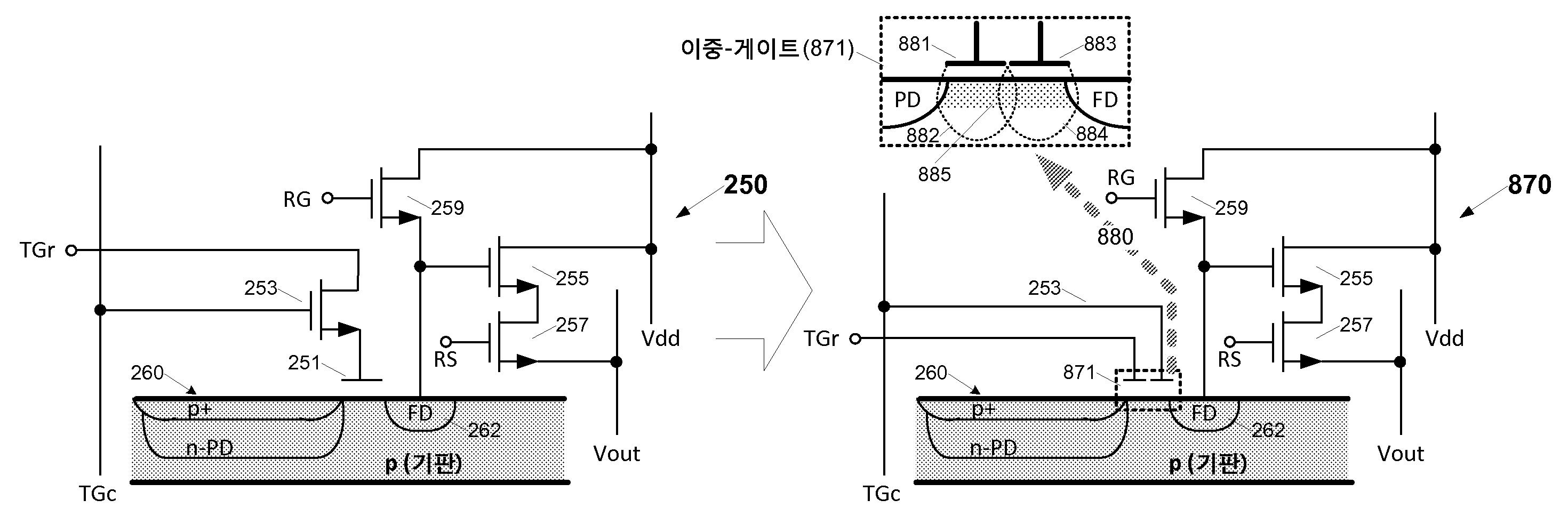
집적 회로 이미지 센서 내의 픽셀 어레이에서, 픽셀 (870) 은 기판 내에 형성된 광검출기 (260) 및 플로팅 확산부 (262) 를 포함한다. 제 1 (881) 및 제 2 (883) 게이트 소자들은 광검출기 및 플로팅 확산부 사이의 기판의 영역 (885) 상부에 서로 인접하게 배치되고, 픽셀 어레이 내에서 행 방향으로 연장되는 행 라인 (TGr) 과, 픽셀 어레이 내에서 열 방향으로 연장되는 열 라인 (TGc) 에 각각 결합된다.In a pixel array in an integrated circuit image sensor, a pixel 870 includes a photodetector 260 and a floating diffusion 262 formed in a substrate. The first 881 and second 883 gate elements are disposed adjacent to each other on an upper portion of the substrate region 885 between the photodetector and the floating diffusion unit, and a row line TGr extending in a row direction in the pixel array And, each of the column lines TGc extending in the column direction in the pixel array.
Description
본 개시물은 전자 이미지 센서들의 분야, 그리고 더욱 구체적으로, 이러한 이미지 센서들에서의 이용을 위한 샘플링 아키텍처 (sampling architecture) 에 관한 것이다.This disclosure relates to the field of electronic image sensors, and more specifically, to a sampling architecture for use in such image sensors.
CMOS 또는 CCD 센서들과 같은 디지털 이미지 센서들은 광센서들에 입사한 광자 (photon) 들 ("캡처된 광") 을 전기 전하 (electric charge) 로 변환하도록 각각 구성된 복수의 감광성 소자 (photosensitive element) 들 ("광센서 (photosensor) 들") 을 포함한다. 다음으로, 전기 전하는 각각의 광센서에 의해 캡처된 광을 나타내는 이미지 데이터로 변환될 수 있다. 이미지 데이터는 캡처된 광의 디지털 표현을 포함하고, 시청 디바이스 상에서 디스플레이할 수 있는 디지털 이미지를 생성하도록 조작되거나 프로세싱될 수도 있다. 이미지 센서들은 광을 전기적 신호 (전하, 전압, 전류 등) 로 변환하도록 구성된 복수의 픽셀 영역들 (예를 들어, 하나 이상의 광센서들 및 부수적인 제어 회로부) 로 분할될 수도 있는 물리적 표면을 갖는 집적 회로 ("integrated circuit; IC") 들 내에 구현된다. 편의상, 이미지 센서 내의 픽셀 영역들은 또한, 이미지 픽셀 ("image pixel; IP") 들로서 지칭될 수도 있고, 픽셀 영역들 또는 이미지 픽셀들의 집합체는 이미지 센서 영역으로서 지칭될 것이다. 이미지 센서 IC 는 전형적으로, 이미지 센서 영역의 외부의 구역들, 예를 들어, 어떤 타입들의 제어, 샘플링, 또는 인터페이스 회로부를 또한 포함할 것이다. 대부분의 CMOS 이미지 센서들은 픽셀 전기적 신호들을 디지털 이미지 데이터로 변환하기 위한 A/D (아날로그-디지털) 회로부를 포함한다. A/D 회로부는 이미지 센서 영역 내에 또는 이미지 센서 영역 주변의 주변에 위치된 하나 이상의 ADC (analog-to-digital converter; ADC) 들일 수 있다.Digital image sensors, such as CMOS or CCD sensors, comprise a plurality of photosensitive elements each configured to convert photons (“captured light”) incident on the photosensors into an electric charge. ("Photosensors"). Next, the electrical charge can be converted into image data representing the light captured by each optical sensor. The image data includes a digital representation of the captured light and may be manipulated or processed to produce a digital image that can be displayed on a viewing device. Image sensors are integrated with a physical surface that may be divided into a plurality of pixel regions (e.g., one or more photosensors and ancillary control circuitry) configured to convert light into electrical signals (charge, voltage, current, etc.). It is implemented within circuits ("integrated circuits"). For convenience, pixel regions within an image sensor may also be referred to as image pixels (“image pixels” (IPs)), and pixel regions or collections of image pixels will be referred to as image sensor regions. The image sensor IC will typically also include areas outside of the image sensor area, eg some types of control, sampling, or interface circuitry. Most CMOS image sensors include A/D (analog-digital) circuitry for converting pixel electrical signals into digital image data. The A/D circuit unit may be one or more analog-to-digital converters (ADCs) located in the image sensor area or around the image sensor area.
본원에서 개시된 다양한 실시형태들은, 같은 참조 번호들이 유사한 요소들을 지칭하는 첨부한 도면의 도면들에서 제한이 아니라 예를 통해 예시되어 있으며:
도 1 은 하나의 실시형태에 따라, 이미지 센서의 부분의 단면을 예시하고;
도 2 는 예컨대, 도 1 의 레이아웃에서 유용한 하나의 실시형태에 따라, 다수의 픽셀 신호 임계점 (threshold) 들을 갖는 아날로그 픽셀 이미지 센서의 부분적인 어레이 회로부를 예시하고;
도 3 은 예컨대, 도 1 및 도 2 의 실시형태들에서 유용한 하나의 실시형태에 따라, 픽셀 신호를 멀티-비트 디지털 변환으로 변환하도록 구성된 일 예의 이미지 센서 판독 회로 (image sensor read circuit) 를 예시하고;
도 4 는 예컨대, 도 1 의 단면과, 도 2 및 도 3 의 회로부를 이용하는 하나의 실시형태에 따라, 멀티-비트 아키텍처를 갖는 이미지 센서 시스템의 일 예의 회로 블록도 실시형태를 예시하고;
도 5 는 예컨대, 도 1 의 단면과, 도 2 및 도 3 의 회로부를 이용하는 하나의 실시형태에 따라, IP 어레이 주변에 위치된 판독 회로 어레이들을 갖는 이미지 센서 시스템 아키텍처의 또 다른 예의 회로 블록도를 예시하고,
도 6a 는 예컨대, 도 2 의 어레이 회로부를 이용하는 하나의 실시형태에 따라, 도 4 및 도 5 에 대해 대안적인 일 예의 2-층 이미지 센서 시스템 아키텍처에서의 픽셀 어레이 IC 의 평면도를 예시하고;
도 6b 는 예컨대, 도 3 의 판독 회로부를 이용하는 하나의 실시형태에 따라, 도 4 및 도 5 에 대해 대안적인 일 예의 2-층 이미지 센서 시스템 아키텍처에서의 프리프로세서 IC 의 평면도를 예시하고;
도 6c 는 하나의 실시형태에 따라, 일 예의 2-층 이미지 센서 시스템 아키텍처에서 도 6a 의 픽셀 어레이 IC 및 도 6b 의 프리프로세서 IC 의 부분적인 단면을 예시하고;
도 7 은 하나의 실시형태에 따라, 도 3 의 판독 회로와 같은 이미지 센서 판독 회로의 동작을 예시하고;
도 8 은 본원에서 설명된 시스템들에서 유용한 하나의 실시형태에 따라, 이미지 캡처 시스템에서의 데이터 흐름을 예시하고;
도 9 는 하나의 실시형태에 따라, 도 3 의 판독 회로와 같은 이미지 센서 판독 회로에 의한 이용을 위한 다양한 시간적 샘플링 정책들을 예시하고;
도 10 은 상관된 이중 샘플링 (correlated double sampling) 과 함께 조건부-재설정 동작을 인에이블 (enable) 하기 위하여 비파괴 임계점-초과 검출 (nondestructive over-threshold detection) 동작이 실행되는 변형된 4-트랜지스터 픽셀의 실시형태를 예시하고;
도 11 은 도 10 의 진행형 독출 픽셀 (progressive read-out pixel) 내에서의 예시적인 픽셀 사이클을 예시하는 타이밍도이고;
도 12 및 도 13 은 그 대응하는 개략적인 단면도들 아래에, 도 10 의 광다이오드, 전송 게이트(transfer gate) 및 플로팅 확산부(floating diffusion)에 대한 예시적인 정전 전위 (electrostatic potential) 도면들을 예시하고;
도 14 는 진행형-독출 픽셀 어레이를 가지는 이미지 센서 (300) 의 실시형태를 예시하고;
도 15a 내지 도 15c 는 도 10 내지 도 14 를 참조하여 설명된 진행형 독출 픽셀들과 관련하여 채용될 수도 있는 대안적인 열 독출 회로 (column read-out circuit) 실시형태들을 예시하고;
도 16 은 도 10 내지 도 14 의 실시형태들에서 개시된 행 및 열 전송-게이트 (row and column transfer-gate) 제어 라인들이 추가적인 어레이-횡단 제어 라인들을 요구하지 않으면서 다수의 데시메이션 모드 (decimation mode) 들을 인에이블하는 방식으로 적용될 수도 있는 쿼드-픽셀 (quad-pixel), 공유된 플로팅 확산부 이미지 센서 아키텍처를 예시하고;
도 17 은 도 16 에서 도시된 쿼드-픽셀 아키텍처의 예시적인 물리적 레이아웃을 예시하고;
도 18a 및 도 18b 는 도 16 및 도 17 의 쿼드-픽셀 아키텍처에 대하여 채용될 수도 있는 컬러 필터 어레이 (color filter array; CFA) 패턴들을 예시하고;
도 19 및 도 20 은 도 16 에서 도시된 2x2 쿼드-픽셀 배치를 포함하는 이미지 센서 내에서, 전체-해상도 (비-비닝 (non-binning)) 및 비닝된-모드 (binned-mode) 픽셀 독출 (pixel read-out) 동작들의 예시적인 단계들을 각각 예시하는 타이밍도들을 제시하고;
도 21 은 컬러 필터 어레이와 함께, 4x1 쿼드-픽셀 블록들의 모음에 대하여 실행될 수도 있는 대안적인 비닝 전략을 예시하고;
도 22 는 4x1 쿼드-픽셀 블록들의 선택된 열들로부터 독출된 아날로그 신호들의 전압-비닝을 인에이블하기 위하여 적용될 수도 있는 열-상호접속 (column-interconnect) 아키텍처를 예시하고;
도 23 은 도 21 및 도 22 의 4x1 쿼드-픽셀 아키텍처 내에서의 비닝된-모드 독출 동작들의 예시적인 타이밍도를 예시하고;
도 24 는 도 21 내지 도 23 을 참조하여 설명된 데시메이션 (비닝) 모드에서 동작가능한 4x1 쿼드 픽셀 블록들의 어레이를 가지는 이미지 센서의 더욱 상세한 실시형태를 예시하고;
도 25a 내지 도 25c 는 픽셀 열 내에서의 고-이득 (high-gain) 부분적 독출 및 단위 이득 근접 (near-unity gain) 전체 독출을 초래하기 위하여 이용될 수도 있는 선택가능한-이득 (또는 멀티-이득) 독출 회로의 실시형태를 예시하고;
도 26 은 도 25a 의 멀티-이득 아키텍처 내에서의 하드-재설정 (hard-reset), 적분 (integration), 부분적인 독출 및 (조건부) 전체 독출 동작들 동안의 공통-소스 (common-source) 및 소스-팔로워 (source-follower) 이득 구성들의 교대 적용을 예시하는 예시적인 타이밍도를 제시하고;
도 27 은 픽셀 열 내에서의 고-이득 부분적 독출 및 단위 이득 근접 전체 독출을 초래하기 위하여 이용될 수도 있는 선택가능한-이득 (또는 멀티-이득) 독출 회로의 대안적인 실시형태를 예시하고;
도 28 은 상부 및 하부 독출 회로들 사이에 배치된 픽셀 어레이를 가지는 이미지 센서의 실시형태를 예시하고;
도 29 는 이미지 프로세서, 메모리 및 디스플레이와 함께, 조건부-재설정 이미지 센서를 가지는 이미징 시스템의 실시형태를 예시하고;
도 30 은 이미지 프로세싱 동작과 관련하여 도 29 의 이미징 시스템 내에서 실행될 수도 있는 예시적인 동작들의 시퀀스를 예시하고;
도 31 은 도 10 의 조건부-재설정 픽셀 및 "분할-게이트" 픽셀의 실시형태들을 대조하고;
도 32 는 도 31 의 분할-게이트 픽셀 내에서의 예시적인 픽셀 사이클 (재설정/전하 적분/독출) 을 예시하는 타이밍도이고;
도 33 은 도 31 의 분할-게이트 픽셀의 예시적인 낮은-광 (low-light) 및 높은-광 (high-light) 동작을 예시하여, 광검출기 (photodetector), 이중-제어 전송 게이트 및 플로팅 확산부의 개략적인 단면도들 아래에서, 각각의 경우에 있어서의 정전 전위 도면들을 도시하고;
도 34 는 도 31 의 분할-게이트 픽셀 내에서의 대안적인 임계점초과 검출 동작을 예시하고;
도 35 는 도 31 에서 도시된 이중-제어 게이트의 예시적인 구현예를 예시하고;
도 36 은 도 31 의 이중-제어 게이트 구조를 구현하는 대안적인 방식을 예시하고;
도 37 은, 행 및 열 전송-게이트 제어 라인들의 쌍들이 4 개의 분할-게이트 픽셀들의 각각 내의 이중-게이트 구조에 결합되는 쿼드-픽셀, 공유된 플로팅 확산부 이미지 센서 아키텍처를 예시하고;
도 38 및 도 39 는 도 37 의 쿼드-픽셀의 예시적인 물리적 레이아웃들을 예시하여, 각각의 이중-제어 게이트 구조들을 통해 중앙집중화된 플로팅 확산부 주위에 배치되고 스위칭가능하게 결합된 4 개의 광다이오드들을 도시하고;
도 40 및 도 41 은 전용 행 전송-게이트 (row transfer-gate; TGr) 라인이 없는 대안적인 실시형태에 따라 분할-게이트 픽셀 아키텍처 및 대응하는 타이밍도를 예시하고;
도 42a 는 이중-제어 게이트의 게이트 소자들이 다이오드의 각각의 p-도핑된 및 n-도핑된 영역들에 의해 형성되는 대안적인 이중-제어 게이트 배치를 예시하고;
도 42b 는 이중-제어 게이트의 게이트 소자들이 공유된 n-도핑된 영역을 가지는 백-투-백 (back-to-back) 다이오드들의 각각의 p-도핑된 영역들에 의해 형성되는 또 다른 대안적인 이중-제어 게이트 배치를 예시하고; 그리고
도 43 은 예를 들어, 도 21 을 참조하여 위에서 설명된 바와 같이 비닝된 또는 독립-픽셀 모드들에서 동작될 수도 있는 분할-픽셀들의 4x1 블록 (쿼드, 분할-픽셀 블록) 을 예시한다.The various embodiments disclosed herein are illustrated by way of example and not limitation in the drawings of the accompanying drawings in which like reference numbers refer to like elements:
1 illustrates a cross section of a portion of an image sensor, according to one embodiment;
2 illustrates a partial array circuitry of an analog pixel image sensor having multiple pixel signal thresholds, for example, according to one embodiment useful in the layout of FIG. 1;
FIG. 3 illustrates an example image sensor read circuit configured to convert a pixel signal to a multi-bit digital conversion, for example, according to one embodiment useful in the embodiments of FIGS. 1 and 2. ;
4 illustrates an example circuit block diagram embodiment of an image sensor system having a multi-bit architecture, for example in accordance with the cross section of FIG. 1 and one embodiment using the circuitry of FIGS. 2 and 3;
5 shows a circuit block diagram of another example of an image sensor system architecture with readout circuit arrays located around an IP array, e.g., according to the cross section of FIG. 1 and one embodiment using the circuitry of FIGS. To illustrate,
6A illustrates a top view of a pixel array IC in an example two-layer image sensor system architecture alternative to FIGS. 4 and 5, according to one embodiment using the array circuitry of FIG. 2, for example;
6B illustrates a top view of a preprocessor IC in an example two-layer image sensor system architecture alternative to FIGS. 4 and 5, according to one embodiment using, for example, the readout circuitry of FIG. 3;
6C illustrates a partial cross-section of the pixel array IC of FIG. 6A and the preprocessor IC of FIG. 6B in an example two-layer image sensor system architecture, according to one embodiment;
7 illustrates the operation of an image sensor readout circuit, such as the readout circuit of FIG. 3, according to one embodiment;
8 illustrates data flow in an image capture system, according to one embodiment useful in the systems described herein;
9 illustrates various temporal sampling policies for use by an image sensor readout circuit, such as the readout circuit of FIG. 3, according to one embodiment;
10 is an implementation of a modified 4-transistor pixel in which a nondestructive over-threshold detection operation is performed to enable a conditional-reset operation with correlated double sampling. Exemplify the form;
FIG. 11 is a timing diagram illustrating an exemplary pixel cycle within the progressive read-out pixel of FIG. 10;
12 and 13 illustrate exemplary electrostatic potential diagrams for the photodiode, transfer gate, and floating diffusion of FIG. 10, below their corresponding schematic cross-sectional views. ;
14 illustrates an embodiment of an
15A-15C illustrate alternative column read-out circuit embodiments that may be employed in connection with the progressive read pixels described with reference to FIGS. 10-14;
16 shows a number of decimation modes in which the row and column transfer-gate control lines disclosed in the embodiments of FIGS. 10 to 14 do not require additional cross-array control lines. ) Illustrating a quad-pixel, shared floating diffuser image sensor architecture that may be applied in a manner that enables them;
17 illustrates an example physical layout of the quad-pixel architecture shown in FIG. 16;
18A and 18B illustrate color filter array (CFA) patterns that may be employed for the quad-pixel architecture of FIGS. 16 and 17;
19 and 20 show a full-resolution (non-binning) and a binned-mode pixel readout (in the image sensor including the 2x2 quad-pixel arrangement shown in FIG. 16). present timing diagrams each illustrating exemplary steps of pixel read-out) operations;
21 illustrates an alternative binning strategy that may be implemented for a collection of 4x1 quad-pixel blocks, with a color filter array;
22 illustrates a column-interconnect architecture that may be applied to enable voltage-bining of analog signals read from selected columns of 4x1 quad-pixel blocks;
23 illustrates an example timing diagram of binned-mode read operations within the 4x1 quad-pixel architecture of FIGS. 21 and 22;
Fig. 24 illustrates a more detailed embodiment of an image sensor having an array of 4x1 quad pixel blocks operable in the decimation (binning) mode described with reference to Figs. 21-23;
25A-25C show selectable-gain (or multi-gain) that may be used to result in a high-gain partial readout and a near-unity gain full readout within a pixel column. ) Illustrate the embodiment of the read circuit;
FIG. 26 is a common-source and source during hard-reset, integration, partial read and (conditional) full read operations in the multi-gain architecture of FIG. 25A -Present an exemplary timing diagram illustrating the alternate application of source-follower gain configurations;
27 illustrates an alternative embodiment of a selectable-gain (or multi-gain) readout circuit that may be used to result in a high-gain partial read and a unity gain near full read within a pixel column;
28 illustrates an embodiment of an image sensor having a pixel array disposed between upper and lower read circuits;
29 illustrates an embodiment of an imaging system having a conditionally-reset image sensor, along with an image processor, memory and display;
30 illustrates an example sequence of operations that may be performed within the imaging system of FIG. 29 in connection with an image processing operation;
FIG. 31 contrasts embodiments of the conditionally-reset pixel and "split-gate" pixel of FIG. 10;
FIG. 32 is a timing diagram illustrating an exemplary pixel cycle (reset/charge integration/read) within the split-gate pixel of FIG. 31;
FIG. 33 illustrates an exemplary low-light and high-light operation of the split-gate pixel of FIG. 31, showing a photodetector, a double-controlled transfer gate, and a floating diffusion. Below the schematic cross-sectional views, the electrostatic potential diagrams in each case are shown;
FIG. 34 illustrates an alternative over-threshold detection operation within the split-gate pixel of FIG. 31;
FIG. 35 illustrates an example implementation of the double-control gate shown in FIG. 31;
36 illustrates an alternative way of implementing the double-control gate structure of FIG. 31;
37 illustrates a quad-pixel, shared floating diffuser image sensor architecture in which pairs of row and column transfer-gate control lines are coupled to a double-gate structure in each of four split-gate pixels;
38 and 39 illustrate exemplary physical layouts of the quad-pixel of FIG. 37, with four photodiodes switchably coupled and disposed around a centralized floating diffusion through respective dual-control gate structures. Show;
40 and 41 illustrate a split-gate pixel architecture and corresponding timing diagram according to an alternative embodiment without dedicated row transfer-gate (TGr) lines;
42A illustrates an alternative double-control gate arrangement in which the gate elements of the double-control gate are formed by respective p-doped and n-doped regions of a diode;
Figure 42b is another alternative formed by the respective p-doped regions of back-to-back diodes having an n-doped region in which the gate elements of the double-control gate are shared. Exemplifies a double-control gate arrangement; And
43 illustrates, for example, a 4x1 block of split-pixels (quad, split-pixel block) that may be operated in binned or independent-pixel modes as described above with reference to FIG. 21.
일부의 이미지 센서들에서는, 픽셀 영역에 입사하는 광 (본원에서는 "픽셀 신호" 로서 지칭됨) 으로부터의 광자 응답 및 결과를 나타내는 전기적 정보가 판독 회로부에 의해 디지털 이미지 데이터 값으로 변환된다. 판독 회로부는 이미지 센서 내에 존재할 수 있거나, 이미지 센서 외부에 위치될 수 있다. 일부의 접근법들에서, 판독 회로는 판독 회로에 인접한 또는 근처의 하나 이상의 픽셀 영역들에 의한 이용을 위하여 이미지 센서 내에 위치될 수 있다. 이미지 센서의 외부에 위치된 판독 회로들을 위하여, 판독 회로들과 연관된 하나 이상의 픽셀 영역들의 픽셀 신호들은 픽셀 영역들로부터 판독 회로들로 전송될 수 있다.In some image sensors, electrical information representing the photon response and result from light incident on a pixel area (referred to herein as a “pixel signal”) is converted into a digital image data value by a readout circuit portion. The readout circuitry may exist within the image sensor or may be located outside the image sensor. In some approaches, the readout circuit may be located within the image sensor for use by one or more pixel regions adjacent or near the readout circuit. For readout circuits located outside of the image sensor, pixel signals of one or more pixel areas associated with the readout circuits may be transferred from the pixel areas to the readout circuits.
각각의 판독 회로는 픽셀 영역을 샘플링하고, 샘플링된 픽셀 영역으로부터 픽셀 신호를 수신하고, 픽셀 신호를, 픽셀 신호를 나타내는 멀티-비트 디지털 값으로 변환한다. 픽셀 신호 또는 픽셀 신호를 나타내는 디지털 값이 샘플링 임계점을 초과할 경우에는, 픽셀 신호와 연관된 픽셀 영역에서 저장된 픽셀 신호는 (예를 들어, 픽셀 영역과 연관된 감광성 소자를 재설정함으로써) 재설정된다. 픽셀 신호 또는 디지털 값이 샘플링 임계점을 초과하지 않을 경우, 픽셀 영역에서 저장된 픽셀 신호는 재설정되지 않는다. 픽셀 신호가 샘플링 임계점을 초과할 때만의 픽셀 영역의 샘플링과, 픽셀 영역에서의 픽셀의 재설정은 본원에서 "조건부 재설정을 갖는 비파괴 샘플링" 으로서 지칭된다.Each readout circuit samples a pixel area, receives a pixel signal from the sampled pixel area, and converts the pixel signal into a multi-bit digital value representing the pixel signal. When the pixel signal or a digital value representing the pixel signal exceeds the sampling threshold, the pixel signal stored in the pixel region associated with the pixel signal is reset (eg, by resetting the photosensitive element associated with the pixel region). If the pixel signal or digital value does not exceed the sampling threshold, the pixel signal stored in the pixel area is not reset. Sampling of the pixel area only when the pixel signal exceeds the sampling threshold, and the resetting of the pixel in the pixel area are referred to herein as "non-destructive sampling with conditional reset".
이미지 센서 개요Image sensor overview
도 1 은 실시형태에서 유용한 이미지 센서 (25) 의 부분적인 단면을 예시한다. 이미지 센서 (25) 에서는, 마이크로렌즈 어레이 (microlens array; 10) 및 (컬러 이미징을 위해 유용한) 컬러 필터 어레이 (12) 를 통과하는 광이 이미지 센서의 실리콘 섹션 (20) 에 입사한다. 마이크로렌즈들 (또는 다른 집광 광학기기들) 및 컬러 필터들의 이용은 선택적이고 예시적인 목적들만을 위해 여기에서 도시되어 있다. 실리콘 (20) 은, 실리콘에 의해 흡수된 광자들에 의해 생성된 전하를 수집하기 위한 광다이오드들 (도시되지 않음) 과, 광다이오드들을 동작시키기 위한 액세스 트랜지스터들 (또한, 도시되지 않음) 을 포함한다. 픽셀 어레이 IC 배선 (14) 은 어레이 내에서 신호들 및 공급 전압들을 보내기 위해 이용된 접속들을 제공한다. 도시된 바와 같이, 광이 배선 층들 및 주요 능동 회로 형성부와 반대인 집적 회로의 측부로부터 실리콘에 진입하므로, 이미지 센서 (25) 는 후면 조명식 (BackSide Illuminated; BSI) 센서이다. 선택적으로, 픽셀 어레이 IC 배선 (14) 은 전면 조명 (FrontSide Illumination; FSI) 을 위하여 컬러 필터 어레이 (12) 및 (도 1 에서 배향된 바와 같이 실리콘의 "상단 (top)" 내에 주요 능동 회로 형성부를 갖는) 실리콘 (20) 사이에 배치될 수 있다.1 illustrates a partial cross section of an image sensor 25 useful in an embodiment. In the image sensor 25, light passing through a
이미지 센서 (25) 는, 마이크로렌즈 어레이 (10) 의 렌즈들에 의해 수집된 광이 각각 입사하는 복수의 IP 들 ("이미지 픽셀들"), 도시된 IP1 내지 IP3 을 포함한다. 각각의 IP 는 실리콘 (20) 내에 내장된 하나 이상의 광다이오드들을 포함한다. 실리콘 (20) 에 진입하는 적어도 일부의 광자들은 실리콘에서 전자-정공 쌍 (electron-hole pair) 들로 변환되고, 결과적인 전자들 (또는 대안적인 실시형태들에서의 정공들) 은 IP 들에 의해 수집된다. 본원에서의 설명은 간략함의 목적들을 위하여 이 프로세스를 이미지 데이터로의 IP 들에 의한 광의 캡처 및 변환으로서 지칭할 것이다. 이미지 센서의 각각의 IP 는 이미지 센서의 표면 구역의 부분을 나타내고, 이미지 센서의 IP 들은 열들 및 행들의 다양한 어레이들로 편성될 수도 있다. CMOS 또는 CCD 이미지 픽셀 기술에서, 각각의 IP (예를 들어, 각각의 광센서) 는 IP 에 입사한 광을 전하로 변환하고, 전하를 전압 또는 전류로 변환하도록 구성된 독출 회로부를 포함한다. 다른 실시형태들에서는, 다수의 IP 들로부터의 이미지 데이터가 더 적은 수 (하나 이상) 의 픽셀들을 나타내기 위하여 조합되지만 (다운샘플링), 하나의 실시형태에서는, 이미지 센서의 각각의 IP 에 의해 캡처된 광은 연관된 디지털 이미지에 대한 이미지 데이터의 하나의 픽셀을 나타낸다.The image sensor 25 includes a plurality of IPs ("image pixels") to which light collected by the lenses of the
이미지 센서 (25) 는 IP 어레이 외부에서 컴포넌트 (component) 들을 포함할 수도 있다. 유사하게, IP 어레이의 부분들은 광을 전하로 변환하지 않는 컴포넌트들을 포함할 수도 있다. 집합체에서의 IP 들에 의해 정의된 영역은 이미지 센서 영역으로서 지칭될 것이다. 본원에서 설명된 바와 같이, 이미지 센서는 증폭기들, 아날로그-디지털 변환기 ("ADC") 들, 비교기들, 제어기들, 카운터들, 누적기 (accumulator) 들, 레지스터 (register) 들, 트랜지스터들, 광다이오드들 등을 포함할 수도 있다. 상이한 아키텍처들에서, 이 컴포넌트들의 일부는 이미지 센서 영역 내에 또는 이미지 센서 영역 외부에 위치될 수도 있고, 일부의 컴포넌트들은 동반된 집적 회로 상에 위치될 수도 있다. 이 실시형태들에서, (마이크로렌즈 어레이 (10) 의 렌즈들과 같은) 렌즈는 예를 들어, 증폭기들, 비교기들, 제어기들, 및 다른 컴포넌트들 상에서가 아니라, IP 내에서 실제적인 광-감지 소자들을 향해 광을 지향시키도록 구성될 수도 있다.Image sensor 25 may include components outside the IP array. Similarly, portions of an IP array may contain components that do not convert light into charge. The area defined by the IPs in the aggregate will be referred to as the image sensor area. As described herein, image sensors include amplifiers, analog-to-digital converters ("ADCs"), comparators, controllers, counters, accumulators, registers, transistors, optical It may also include diodes and the like. In different architectures, some of these components may be located within the image sensor area or outside the image sensor area, and some components may be located on an accompanying integrated circuit. In these embodiments, the lens (such as the lenses of the microlens array 10) is not for example on amplifiers, comparators, controllers, and other components, but the actual light-sensing within IP. It may be configured to direct light towards the elements.
위에서 언급된 바와 같이, 이미지 센서는 다수의 IP 들의 어레이를 포함할 수도 있다. 각각의 IP 는 광 (예를 들어, 하나 이상의 광자들) 에 응답하여, 대응하는 전하를 캡처하고 저장한다. 하나의 실시형태에서, IP 를 샘플링할 시에, IP 에서 저장된 전하를 나타내는 픽셀 신호가 샘플링 임계점을 초과할 경우, 픽셀 신호는 픽셀 신호를 나타내는 디지털 값으로 변환되고 IP 에 의해 저장된 전하는 재설정된다. 대안적으로, IP 를 샘플링할 시에, IP 에서 저장된 전하를 나타내는 픽셀 신호는 픽셀 신호를 나타내는 디지털 값으로 변환되고, 디지털 값이 샘플링 임계점을 초과할 경우, IP 에 의해 저장된 전하는 재설정된다. 다른 실시형태들에서, 아날로그-디지털 변환이 시작되고, 임계점이 초과되는지 여부를 결정하기 위하여 충분한 변환이 완료되었을 때, 변환을 계속할 것인지 여부에 대한 결정이 행해진다. 예를 들어, 연속 근사화 레지스터 ("successive approximation register; SAR") ADC 에서는, 임계점이 최상위 비트 (most-significant-bit) (들) 패턴과 동일할 경우, 패턴이 분해되자마자, 변환을 계속하고, 픽셀의 재설정을 수행하거나 변환을 중지할 것인지 여부에 대한 결정이 행해질 수 있다. 픽셀 신호 또는 픽셀 신호를 나타내는 디지털 값이 샘플링 임계점을 초과하는지 여부의 결정은 픽셀 신호 또는 디지털 값을 샘플링 임계점과 비교하도록 구성된 비교기의 이용을 통해 행해질 수 있다.As mentioned above, an image sensor may contain an array of multiple IPs. Each IP responds to light (eg, one or more photons) to capture and store a corresponding charge. In one embodiment, upon sampling IP, if the pixel signal representing the stored charge in IP exceeds the sampling threshold, the pixel signal is converted to a digital value representing the pixel signal and the stored charge by IP is reset. Alternatively, upon sampling IP, the pixel signal representing the charge stored in IP is converted to a digital value representing the pixel signal, and when the digital value exceeds the sampling threshold, the charge stored by IP is reset. In other embodiments, when analog-to-digital conversion is started and sufficient conversion has been completed to determine whether a threshold is exceeded, a determination is made as to whether to continue conversion. For example, in a "successive approximation register (SAR") ADC, if the threshold is equal to the most-significant-bit(s) pattern, the conversion continues as soon as the pattern is resolved, A decision may be made as to whether to perform a pixel reset or stop conversion. The determination of whether the pixel signal or digital value representing the pixel signal exceeds a sampling threshold may be made through use of a comparator configured to compare the pixel signal or digital value to the sampling threshold.
도 2 는 하나의 실시형태에 따라, 다수의 픽셀 신호 임계점들을 갖는 아날로그 픽셀 이미지 센서를 예시한다. 도 2 의 이미지 센서는 CMOS 센서이고, IP 어레이 (40) 를 포함한다. IP 어레이는 열 당, 그리고 행 당 임의의 수의 IP 들을 갖는 임의의 수의 열들 및 행들을 포함할 수 있다. IP 열 (50), IP 어레이에서 전체 또는 부분적인 IP 열들을 나타내는 열은 도 2 에서 강조표시된다. IP 열 (50) 은 열 라인 (55) 을 통해 통신가능하게 결합된 복수의 IP 들을 포함한다. IP (60), IP 어레이에서 IP 들을 나타내는 IP 는 도 2 에서 강조표시된다.2 illustrates an analog pixel image sensor having multiple pixel signal thresholds, according to one embodiment. The image sensor of FIG. 2 is a CMOS sensor and includes an
IP (60) 는, 광다이오드가 노출을 위한 준비 시에 사전충전되고, 다음으로, 노출 후에 샘플링되는 것을 인에이블하는 제어 소자들과 함께, 광다이오드 (65) 를 포함한다. 동작 시에, 광다이오드의 캐소드를 전압원에 결합하여, 이에 따라, 광다이오드의 캐소드를 사전충전 전압으로 "사전충전" 하기 위하여, 트랜지스터 (70) 가 스위치 온 (switch on) 된다. 트랜지스터 (70) 는 노출 구간의 시작 시에 또는 그 시작 전에 스위치 오프 (switch off) 된다. 트랜지스터 (70) 오프에 의해, 캐소드 전압은 광자 타격 (photon strike) 들에 응답하여 증가 방식으로 방전하여, 검출된 광의 양에 비례하여 광다이오드 전위 VDET 를 저하시킨다. 노출 구간의 종결 시에, 액세스 광다이오드 전위를 나타내는 신호가 팔로워-트랜지스터 (74) 를 통해 픽셀 신호 (80) 로서 열 라인 (55) 상으로 증폭/구동되는 것을 인에이블하기 위하여, 액세스 트랜지스터 (72) 가 스위치 온 된다.
ADC (85) 는 열 버스 (55) 를 통해 IP 열 (50) 에 통신가능하게 결합된다. 도 2 의 실시형태에서, ADC 는 픽셀 어레이 (40) 의 에지 (edge) 에 위치되고, IP 어레이가 그 위에 위치되는 이미지 센서 내에 또는 이미지 센서 외부에 위치될 수도 있다. ADC 는 IP (60) 로부터 픽셀 신호 (80) (아날로그 광다이오드 전위의 표현) 를 수신한다. ADC 는 픽셀 신호를 나타내는 3-비트 디지털 값 ("Pix[2:0]") 을 생성하기 위하여 픽셀 신호를 디지털화한다. ADC 는 7 개의 픽셀 임계점들, 임계점 1 내지 임계점 7 (본원에서 "VT1 내지 VT7" 로서 지칭됨) 을 포함한다. 픽셀 신호의 크기가 Vpre 보다 더 작지만 VT1 보다 더 클 경우, ADC 는 픽셀 신호를 디지털 값 "000" 으로 변환한다. VT1 보다 더 작지만 VT2 보다 더 큰 픽셀 신호들은 디지털 값 "001" 로 변환되고, VT2 및 VT3 사이의 픽셀 신호들은 "010" 으로 변환되고, "111" 로 변환되는 VT7 보다 더 작은 픽셀 신호들까지, 이하 등등과 같다.
도 2 의 실시형태에서, 연속적인 픽셀 임계점들 사이의 전위차는 대략 동일하다 (예컨대, VT3 - VT4 ![]()
![]()
Vfloor 는, 광다이오드 (65) 의 캐소드 전압이 광자 타격들에 응답하여 이제 더 이상 선형적으로 방전하지 않는 픽셀 포화 임계점을 나타낸다. 선형 감도 영역 (linear sensitivity region; 90) 내의 픽셀 신호들에 대하여, 디지털 값들로의 픽셀 신호들의 변환은 그래프 (95) 로 도시된다. 검출가능한 광자 타격들 (즉, 픽셀 포화 포인트) 의 최대 수는 광다이오드의 커패시턴스, 그리고 이에 따라, 그 물리적 사이즈에 비례한다는 것에 주목해야 한다. 결과적으로, 전통적인 센서 설계에서는, 광다이오드 풋프린트 (footprint) 가 소정의 애플리케이션에서 요구되는 동적 범위에 의해 기술되고, 축소 프로세스 기하구조들로 두드러지게 스케일링되지 않는다.V floor represents the pixel saturation threshold at which the cathode voltage of
이미지의 캡처 동안, 하나의 실시형태에서는, IP 어레이 (40) 에서의 IP 열 (50) 및 서로의 열에서의 소정의 행 또는 행들의 IP 들이 연속적으로 샘플링되고, 각각과 연관된 픽셀 신호들은 각각의 열과 연관된 ADC 또는 ADC 들을 이용하여 디지털 값들로 변환된다. ADC 들에 의해 출력된 디지털 값들은 이미지 캡처 주기 동안에 (이하에서 설명된 바와 같이, 일부의 실시형태들에서는 조건부로) 누적되고 저장된다. 도 2 에서 예시된 것과는 다른 타입들 및 구성들의 IP 들이 이미지 센서 시스템에서 이용될 수 있다. 예를 들어, 트랜지스터들 (70, 72, 및 74) 과는 상이한 배치의 트랜지스터들이 이용될 수 있다. 게다가, 하나의 ADC (85) 가 IP 열 (50) 과 함께 도 2 에서 도시되어 있지만, 다른 실시형태들에서는, 하나를 초과하는 ADC 가 IP 열 당 이용될 수 있고, 상이한 ADC 그룹들은 ADC 열의 어레이 행들의 상이한 섹션들에 작용할 수 있다. ADC 들 (판독 회로들의 형태) 및 IP 들의 추가적인 조합들은 이하에서 더욱 상세하게 설명된다. 최종적으로, ADC 의 출력 (예컨대, 도 2 의 실시형태에서의 Pix[2:0]) 은 임의의 멀티-비트 길이일 수 있고, Vpre 및 Vfloor 사이에서 임의의 방식으로 분포된 임의의 수의 임계점들과 연관될 수 있다.During the capture of the image, in one embodiment, the
멀티-비트 샘플링 및 조건부 재설정을 갖는 이미지 센서 시스템Image sensor system with multi-bit sampling and conditional reset
도 3 은 하나의 실시형태에 따라, 픽셀 신호를 멀티-비트 디지털 변환으로 변환하도록 구성된 일 예의 이미지 센서 판독 회로를 예시한다. 도 3 의 실시형태는 IP (100), IP 메모리 (116), 및 판독 회로 (110) 를 예시하고, 판독 회로는 ADC/비교기 회로 (112) (이하, "ADC/비교기") 및 가산기 (114) 를 포함한다. 다른 실시형태들에서, 도 3 의 모듈들은 추가적인, 더 적은, 및/또는 상이한 컴포넌트들을 포함할 수 있는 것에 주목해야 한다. 예를 들어, ADC/비교기는 별도의 컴포넌트들로서 구현될 수 있고, 가산기는 판독 회로의 외부에 위치될 수 있다.3 illustrates an example image sensor readout circuit configured to convert a pixel signal into a multi-bit digital conversion, according to one embodiment. The embodiment of Fig. 3 illustrates the
IP (100) 는 이미지 센서에서의 IP 를 나타내고, 예를 들어, 도 2 의 IP (60) 일 수 있다. IP (100) 는 예를 들어, 외부 제어 로직으로부터 하나 이상의 제어 신호들을 수신한다. 제어 신호는 예를 들어, Vpre 와 관련한 전하의 저장으로 귀착되도록 하기 위하여, IP 를 Vpre 로 재설정하고 광에 대한 IP 의 감광성 소자의 노출을 인에이블함으로써, IP 가 이미지 캡처를 시작하는 것을 인에이블할 수 있다. 유사하게, 제어 신호는 예를 들어, 이미지 캡처 주기의 경과 후에 광에 대한 IP 의 감광성 소자의 노출을 디스에이블 (disable) 함으로써, IP 가 이미지 캡처를 종료하는 것을 인에이블할 수 있다. 제어 신호는 또한, IP 에 의한 픽셀 신호의 출력과, 판독 회로에 의한, 픽셀 신호를 나타내는 디지털 값으로의 픽셀 신호의 변환 (본원에서, "IP 를 샘플링하는 것" 또는 "픽셀 신호들을 샘플링하는 것" 으로서 지칭됨) 을 인에이블할 수 있다. 위에서 설명된 바와 같이, 픽셀 신호는 적분된 전하의 표현 (예컨대, 적분된 전하에 비례하는 성분을 가지는 소스 팔로워 전압, 증폭된 전압, 또는 전류) 일 수 있다.
IP (100) 는 예를 들어, 외부 제어 로직으로부터 재설정 신호를 수신한다. 재설정 신호는 예를 들어, 이미지 캡처 주기의 시작 시에 IP 에 의해 저장된 전하를 Vpre 로 재설정한다. IP 는 또한, ADC/비교기 (112) 로부터 조건부 재설정 신호를 수신한다 (일부의 회로들에서, 조건부 재설정 및 초기 재설정은 공통 회로부를 이용하여 공급됨). 조건부 재설정 신호는 예를 들어, IP 가 샘플링될 때에 픽셀 신호가 샘플링 임계점을 초과하는 것에 응답하여, 이미지 캡처 주기 동안에 IP 에 의해 저장된 전하를 재설정한다. 다른 실시형태들에서는, 조건부 재설정 신호가 상이한 엔티티 (entity) 로부터 수신되는 것에 주목해야 한다. 하나의 구현예에서, ADC/비교기는 픽셀 신호가 샘플링 임계점을 초과하는 것으로 결정할 수도 있고, 외부 제어 로직이 조건부 재설정 신호를 IP 에 출력하는 것을 인에이블할 수도 있고; 이러한 실시형태에서, 재설정 신호 (행-관련 (row-wise) 신호) 및 조건부 재설정 신호 (열-관련 (column-wise) 신호) 는 모든 재설정들을 개시하기 위하여 IP 에 의해 AND 연산될 수도 있다. 간략함을 위하여, 설명의 나머지는 ADC/비교기가 조건부 재설정 신호들을 IP 에 제공하는 실시형태들로 제한될 것이다.
판독 회로 (110) 는 예를 들어, 외부 제어 로직으로부터 임계점 신호, 샘플 신호 (또는 "샘플 인에이블 신호"), 비교 신호 (또는 "비교 인에이블 신호"), 잔차 신호 (또는 "잔차 인에이블 신호"), 및 재설정 신호를 수신하고, IP (100) 로부터 픽셀 신호들을 수신한다. IP (100) 에 대응하는 IP 메모리 소자 (116) 는 가산기 (114) 에 의한 독출/기록을 위하여, 그리고 외부 독출을 위하여 그것을 선택하는 독출 신호를 수신한다. ADC/비교기 (112) 는 하나 이상의 샘플 신호들을 수신하는 것에 응답하여 IP (100) 를 샘플링한다. 이미지 캡처 동안, ADC/비교기는 예를 들어, 주기적으로, 또는 사전-정의된 샘플링 구간 패턴 (본원에서는 "샘플링 정책" 으로서 지칭됨) 에 따라 다양한 샘플링 구간들에서 샘플 신호를 수신한다. 대안적으로, ADC/비교기에 의해 수신된 샘플 신호는 샘플링 정책을 포함할 수 있고, ADC/비교기는 샘플링 정책에 기초하여 IP 를 샘플링하도록 구성될 수 있다. 다른 실시형태들에서, IP 는 하나 이상의 샘플 신호들을 수신하고, 수신된 샘플 신호들에 기초하여 픽셀 신호들을 출력한다. 또 다른 실시형태들에서는, IP 가 주기적으로 또는 샘플링 정책에 따라 픽셀 신호들을 출력하거나, ADC/비교기가 수신된 샘플 신호들에 관계 없이, 주기적으로 또는 샘플링 정책에 따라 픽셀 신호들을 샘플링한다. ADC/비교기는 IP 로부터의 픽셀 신호를 샘플링하기 이전에 IP 로부터 픽셀 신호를 요청할 수 있다.The
IP 의 샘플링 동안, ADC/비교기 (112) 는 IP 로부터 픽셀 신호를 수신하고, (선택적으로, 일부의 실시형태들에서는, 픽셀 신호가 샘플링 임계점을 초과하는 것에 기초하여) 픽셀 신호를, 픽셀 신호를 나타내는 다수-비트 디지털 값으로 변환한다. 픽셀 신호가 샘플링 임계점을 초과할 경우, ADC/비교기는 IP 에서 저장된 전하를 재설정하기 위한 조건부 재설정 신호를 출력한다. 픽셀 신호가 샘플링 임계점을 초과하지 않을 경우, ADC/비교기는 IP 에서 저장된 전하를 재설정하기 위한 조건부 재설정 신호를 출력하지 않는다. 샘플링 임계점은 이미지 캡처 동안에 변동될 수 있고 임계점 신호를 통해 수신될 수 있거나, 소정의 이미지 캡처에 대하여 미리 결정되거나 사전설정될 수 있다. 하나의 샘플링 임계점이 다수의 이미지 캡처들 동안에 이용될 수 있고, 상이한 샘플링 임계점들이 상이한 이미지 캡처들에 대해 이용될 수 있고, 다수의 샘플링 임계점들이 단일 이미지 캡처 동안에 이용될 수 있다. 하나의 실시형태에서, 샘플링 임계점은 검출된 변경되는 광 조건들에 응답하여 변동된다 (예를 들어, 샘플링 임계점은 낮은 광 조건들에 응답하여 감소할 수 있고, 높은 광 조건들에 응답하여 증가할 수 있음).During the sampling of IP, ADC/
하나의 실시형태에서, 샘플링 임계점은 아날로그 신호 임계점이다. 이 실시형태에서, ADC/비교기 (112) 는 아날로그 비교기를 포함하고, 픽셀 신호가 샘플링 임계점을 초과하는지를 결정하기 위하여 픽셀 신호를 샘플링 임계점과 비교한다. 픽셀 신호가 IP (100) 에 의해 저장된 전하를 나타내는 전압을 포함할 경우, 픽셀 신호가 샘플링 임계점보다 더 낮을 경우에 샘플링 임계점이 초과된다. 도 2 의 실시형태를 일 예로서 이용하면, ADC/비교기의 샘플링 임계점이 임계점 4 일 경우에는, 픽셀 신호가 임계점 4 와 연관된 전압보다 더 낮은 전압을 포함할 경우에만 픽셀 신호가 샘플링 임계점을 초과할 것이다.In one embodiment, the sampling threshold is an analog signal threshold. In this embodiment, the ADC/
하나의 실시형태에서, 샘플링 임계점은 디지털 신호 임계점이다. 이 실시형태에서, ADC/비교기 (112) 는 디지털 비교기를 포함하고, 먼저, 픽셀 신호를, 픽셀 신호를 나타내는 디지털 값으로 변환한다. 다음으로, ADC/비교기는 픽셀 신호가 샘플링 임계점을 초과하는지를 결정하기 위하여 디지털 값을 샘플링 임계점과 비교한다. 도 2 의 실시형태를 일 예로서 이용하면, "101" 의 샘플링 임계점에 대하여, ADC/비교기가 픽셀 신호를 (픽셀 신호가 임계점 1 및 임계점 2 사이에 있음을 표시하는) "001" 의 디지털 값으로 변환할 경우, 픽셀 신호는 샘플링 임계점을 초과하지 않고 조건부 재설정 신호는 출력되지 않는다. 그러나, ADC/비교기가 픽셀 신호를 (픽셀 신호가 임계점 6 및 임계점 7 사이에 있음을 표시하는) "110" 의 디지털 값으로 변환할 경우, 픽셀 신호는 샘플링 임계점을 초과하고 조건부 재설정 신호는 출력된다.In one embodiment, the sampling threshold is a digital signal threshold. In this embodiment, the ADC/
또 다른 실시형태에서, 샘플링 임계점은 픽셀 신호의 디지털 변환을 완료하기 전에 평가될 수 있는 디지털 신호 임계점이다. 이것은 필요하지 않은 ADC 동작들을 회피함으로써, 픽셀의 더 신속한 조건부 재설정, 및/또는 전력 절감을 허용하기 위한 일부의 실시형태들 또는 이용 사례들에서 유리할 수 있다. 예를 들어, 연속 근사화 레지스터 ADC 에 있어서, 픽셀 신호의 디지털 표현을 분해하기 위하여 다수의 클록 사이클들이 이용된다. 모든 비트 위치들이 분해될 때까지, 제 1 클록 사이클은 최상위 비트를 분해하고, 제 2 클록 사이클은 다음 최상위 비트를 분해하는, 등등과 같다. 도 2 의 실시형태를 일 예로서 이용하면, "100" 의 샘플링 임계점에 대하여, 임계점이 충족되는지 아닌지 여부의 결정은 제 1 SAR ADC 클록 사이클 후에 분해될 수 있다. "110" 의 샘플링 임계점에 대하여, 임계점이 충족되는지 아닌지 여부의 결정은 제 2 SAR ADC 클록 사이클 후에 분해될 수 있다. 예컨대, 6 또는 8 비트들의 비트 심도 (bit depth) 를 갖는 실시형태들에 대하여, 하나 또는 둘의 변환 사이클 후에 재설정 결정을 행하는 것은 상당한 시간/전력 절감들로 귀착될 수 있고, 이것은 0 인 하나 이상의 LSB 들을 갖는 샘플링 임계점을 선택함으로써 실현될 수 있다.In yet another embodiment, the sampling threshold is a digital signal threshold that can be evaluated prior to completing digital conversion of the pixel signal. This may be advantageous in some embodiments or use cases to allow for faster conditional reset of the pixel, and/or power savings, by avoiding unnecessary ADC operations. For example, in a successive approximation register ADC, multiple clock cycles are used to decompose the digital representation of the pixel signal. Until all bit positions have been resolved, the first clock cycle resolves the most significant bit, the second clock cycle resolves the next most significant bit, and so on. Using the embodiment of FIG. 2 as an example, for a sampling threshold of "100", the determination of whether the threshold is met or not can be resolved after a first SAR ADC clock cycle. For a sampling threshold of "110", the determination of whether the threshold is met or not can be resolved after the second SAR ADC clock cycle. For example, for embodiments with a bit depth of 6 or 8 bits, making a reset decision after one or two conversion cycles can result in significant time/power savings, which can result in one or more This can be realized by selecting a sampling threshold with LSBs.
하나의 실시형태에서, 행-관련 비교 신호는 각각의 ADC/비교기 "비교" 신호 입력에 공급되고, 비교를 수행하기 위한 적절한 클록 사이클에 대하여 ADC/비교기에 시그널링한다. 비교 신호가 어써팅 (asserting) 될 때, 비교는 아날로그-디지털 변환의 현재의 상태에 기초하여 수행된다. 임계점이 ADC/비교기 (112) 에 대한 비교에 의해 충족될 경우, 조건부 재설정 신호는 IP (100) 및 가산기 (114) 에 어써팅되고, SAR ADC 는 픽셀 신호를 변환하는 것을 계속한다. 임계점이 충족되지 않을 경우, 조건부 재설정 신호는 어써팅되지 않고, SAR ADC 의 클록 신호를 게이팅 (gating) 하여 변환을 종결시키기 위하여 비교 신호와 함께 이용될 수 있다.In one embodiment, a row-related comparison signal is supplied to each ADC/comparator “compare” signal input and signals the ADC/comparator for an appropriate clock cycle to perform the comparison. When the comparison signal is asserted, the comparison is performed based on the current state of the analog-to-digital conversion. When the threshold is satisfied by comparison to ADC/
ADC/비교기 (112) 는 ADC/비교기에 의해 수신된 픽셀 신호를 나타내는 디지털 값 (본원에서는 "디지털 변환" 으로서 지칭됨) 을 가산기 (114) 에 출력한다. ADC/비교기 (112) 는 샘플링 임계점을 초과하는 디지털 변환과 연관된 픽셀 신호에 응답하여 디지털 변환을 출력할 수 있다. 조건부 재설정 신호는, 디지털 변환을 로딩하고 그것을 (이 실시형태에서는, 독출 라인의 어드레스 선택에 의해 복수의 이러한 로케이션들로부터 선택되는) IP (100) 에 대응하는 IP 메모리 (116) 로케이션 (location) 에 가산하기 위하여 가산기 (114) 에 시그널링하기 위한 인에이블로서 이용될 수 있다. 다른 실시형태들에서, ADC/비교기는 디지털 변환과 연관된 픽셀 신호가 샘플링 임계점을 초과하는지 여부에 관계 없이, IP (100) 의 각각의 샘플링 동안에 디지털 변환을 출력한다. 이 실시형태들에서, 가산기는 샘플링 임계점을 초과하는 픽셀 신호들과 연관된 디지털 변환들을 누적하고, 샘플링 임계점을 초과하지 않는 픽셀 신호들과 연관된 디지털 변환들을 무시하도록 구성될 수 있다. 대안적으로, 임계점이 예를 들어, 도 2 에서 "001" 로 설정될 경우, 가산기는 정확한 결과들을 여전히 생성하면서, IP (100) 가 판독될 때마다 디지털 변환을 IP 메모리 (116) 에 무조건적으로 가산할 수 있다.The ADC/
하나의 실시형태에서, ADC/비교기 (112) 는 또한, (비교 신호가 어써팅되지 않으면서) 잔차 신호 어써션 (assertion) 을 수신하는 것에 응답하여 디지털 변환을 출력한다. 잔차 신호 어써션은 이미지 캡처의 종료와 연관되고, 디지털 변환과 연관된 픽셀 신호가 샘플링 임계점을 초과하고 조건부 재설정을 어써팅하는지 여부에 관계 없이, ADC/비교기가 전체 디지털 변환을 가산기 (114) 에 출력하는 것을 인에이블한다. 잔차 신호는 IP (100) 에 의해 수신된 광과 연관된 이미지 정보의 손실을 방지할 수 있지만, 캡처 주기의 종료 시에 임계점을 능가할 수 없다. 이러한 수신된 광을 나타내는 픽셀 신호가 샘플링 임계점을 초과하지 않을 경우, ADC/비교기는 이와 다르게, 픽셀 신호와 연관된 디지털 변환을 출력하지 않을 수도 있고, IP 에 의해 저장된 전하는 (잔차 신호의 어써션에 의해 또한 트리거링 (triggering) 되는) 조건부 재설정 신호에 의해 재설정되지 않을 것이다. ADC/비교기가 디지털 변환들과 연관된 픽셀 신호들이 샘플링 임계점을 초과하는지 여부에 관계 없이 디지털 변환들을 가산기에 출력하는 실시형태들에서, 가산기는 잔차 신호를 수신할 수 있고, 신호를 수신하는 것에 응답하여 캡처 주기의 종료 시에 수신된 픽셀 신호와 연관된 디지털 변환을 누적하도록 구성될 수 있다.In one embodiment, ADC/
가산기 (114) 는 캡처 주기 동안에 수신된 디지털 변환들을 누적하도록 구성된다. 위에서 논의된 바와 같이, 디지털 변환들과 연관된 픽셀 신호들이 샘플링 임계점을 초과할 경우에만, ADC/비교기 (112) 가 디지털 변환들을 출력하는 실시형태들에서는, 가산기가 (잔차 신호를 수신하는 것에 응답하여 ADC/비교기에 의해 출력된 추가적인 디지털 변환을 포함하는) 모든 수신된 디지털 변환들을 IP 메모리 (116) 내로 누적한다. ADC/비교기가 각각의 수신된 픽셀 신호와 연관된 디지털 변환들을 출력하는 실시형태들에서, 가산기는 샘플링 임계점을 초과하는 픽셀 신호들과 연관된 디지털 변환들과, 잔차 신호를 수신하는 것에 응답하여 ADC/비교기에 의해 출력된 디지털 변환만을 IP 메모리 (116) 내로 누적하고; 이러한 실시형태들은 가산기가 픽셀 신호들이 샘플링 임계점을 언제 초과하는지와, 잔차 신호가 언제 수신되는지를 인지할 것을 요구하고, 간략함의 목적을 위하여 본원에서 추가로 논의되지 않는다.
가산기 (114) 는 예를 들어, 외부 제어 로직으로부터 재설정/가산 제어 시그널링을 수신한다. (예를 들어, 이미지 캡처 주기의 시작 시에) 재설정 신호를 수신하는 것에 응답하여, 누적기는 이미지 데이터로서의 수신된 디지털 변환들의 누적을 위해 모두 제로들을 선택된 IP 메모리 로케이션 (116) 에 저장한다. 가산기는 또한 재설정 신호를 수신하고, 수신된 디지털 변환들의 누적을 재설정한다.
대안적인 실시형태들에서, 가산기는 판독 회로 (110) 의 외부에 위치된다. 예를 들어, ADC/비교기는 (예컨대, 다른 ADC 들로부터의 다른 변환들로 멀티플렉싱된) 디지털 채널로의 변환들의 스트림을, 누적 기능을 제공하는 별도의 회로에 출력할 수 있다. 이러한 경우, ADC/비교기는 또한, 0 일 수 있는 "변환 없음" 에 대한 기호 (symbol) 를 출력해야 한다. 하나의 가능성은 디지털 채널 인터페이스에서의 회로 (예컨대, 도 4 에서의 PHY (134)) 가 대역폭을 감소시키기 위하여 디지털 변환들을 코딩하는 것이다. 하나의 실시형태에서의 "변환 없음" 은 "00" 으로서 출력되고, 상부 임계점 초과된 ADC 변환은 "01" 로서 출력되고, 모든 다른 ADC 변환들은 "1xxxxxx" 로서 출력되고, 여기서, x 는 ADC 변환의 분해된 비트들 중의 하나를 나타내고, x 위치들의 수는 ADC 의 비트 심도와 동일하다.In alternative embodiments, the adder is located external to the
하나의 실시형태에서, IP 는 픽셀 신호를 출력하고 동일한 라인 상에서 조건부 재설정을 수신하도록 구성된다. 이 실시형태에서, IP 및 ADC/비교기 (112) 는 공유된 라인 상에서 픽셀 신호 및 조건부 재설정을 교대로 구동한다. 예를 들어, IP 는 샘플 주기의 제 1 부분 동안에 공유된 라인 상에서 픽셀 신호를 출력할 수 있고, 샘플 주기의 제 2 부분 동안에 공유된 라인 상에서 조건부 재설정들을 수신할 수 있다. 최종적으로, ADC/비교기는 공유된 라인 상에서 임계점 신호, 샘플 신호, 및 잔차 신호를 수신할 수 있다. 예를 들어, ADC/비교기는 이미지 캡처의 시작 시에 임계점 신호를 수신할 수 있고, 이미지 캡처 주기 전반에 걸쳐 샘플 신호들을 수신할 수 있고, 이미지 캡처 주기의 종료 시에 잔차 신호를 수신할 수 있다. 또한, IP 에 의해 수신된 재설정 신호는 누적기 (114) 에 의해 수신된 동일한 재설정 신호일 수 있고, 공유된 라인 상에서 수신될 수 있는 것에 주목해야 한다.In one embodiment, IP is configured to output a pixel signal and receive conditional reset on the same line. In this embodiment, IP and ADC/
도 4 는 하나의 실시형태에 따라, 멀티-비트 아키텍처를 갖는 이미지 센서 시스템의 일 예의 실시형태를 예시한다. 도 4 의 이미지 센서 시스템 (120) 은 이미지 센서 영역 (125), 판독 회로 어레이 (130), 제어 로직 (132), 및 물리적 시그널링 인터페이스 (134) 를 포함한다. 다른 실시형태들에서, 이미지 센서 시스템은 도 4 의 실시형태에서 예시된 것보다 더 적은, 추가적인, 또는 상이한 컴포넌트들을 포함할 수도 있다 (예를 들어, 회로는 그와 함께 집적된 메모리 (116) 를 가질 수도 있음). 도 4 에서 도시된 이미지 센서 시스템은 단일 IC 로서 구현될 수 있거나, 다수의 IC 들로서 구현될 수 있다 (예를 들어, 이미지 센서 영역 및 판독 회로 어레이는 별도의 IC 들 상에 위치될 수 있음). 또한, (판독 회로 어레이, 제어 로직, 및 물리적 시그널링 인터페이스와 같은) 다양한 컴포넌트들은 이미지 센서 영역 (125) 내에서 집적될 수 있다.4 illustrates an example embodiment of an image sensor system having a multi-bit architecture, according to one embodiment. The image sensor system 120 of FIG. 4 includes an image sensor region 125, a readout circuit array 130, a
예의 목적들을 위하여, 이미지 센서 시스템 (120) 과, 이미지 센서 시스템에 통신가능하게 결합된 (도 4 에서 도시되지 않은) 호스트 IC 는 카메라 (예컨대, 이동 디바이스 내의 스틸-이미지 또는 비디오 카메라, 소형 카메라, 디지털 SLR 카메라, 단독형 또는 플랫폼-통합형 웹캠, 고해상도 비디오 카메라, 보안 카메라, 자동차 카메라 등) 내에서 주요 이미지 획득 컴포넌트들을 형성하는 것으로 추정된다. 이미지 센서 IC 및 호스트 IC 는, 계측 도구들, 의료용 도구들, 게임용 시스템들 또는 다른 가전제품 디바이스들, 군사용 및 산업용 이미징 시스템들, 수송-관련 시스템들, 공간-기반 이미징 시스템들 등을 제한 없이 포함하는 임의의 이미징 시스템 또는 디바이스의 사실상 내부에서 단독으로, 또는 유사하거나 상이한 이미징 컴포넌트들과 함께 더욱 일반적으로 배치될 수 있다. 이미지 센서 시스템의 동작은 일반적으로, 광에 대한 IP 들의 노출을 통한 이미지 또는 프레임의 캡처, 노출의 결과로서의 저장된 전하의 이미지 데이터로의 변환, 및 저장 매체로의 이미지 데이터의 출력을 포함한다.For illustrative purposes, the image sensor system 120 and a host IC (not shown in FIG. 4) communicatively coupled to the image sensor system include a camera (e.g., a still-image or video camera in a mobile device, a small camera, Digital SLR cameras, standalone or platform-integrated webcams, high-resolution video cameras, security cameras, automotive cameras, etc.) are believed to form the main image acquisition components. Image sensor IC and host IC include, without limitation, metrology tools, medical tools, gaming systems or other consumer electronics devices, military and industrial imaging systems, transport-related systems, space-based imaging systems, etc. May be disposed alone, or more generally with similar or different imaging components, substantially inside of any imaging system or device. The operation of the image sensor system generally includes the capture of an image or frame through exposure of IPs to light, the conversion of stored charge into image data as a result of the exposure, and the output of image data to a storage medium.
이미지 센서 영역 (125) 은 (0 로부터 N-1 까지 인덱싱되는) N-행들 및 (0 로부터 M-1 까지 인덱싱되는) M-열들을 포함하는 IP 어레이 (127) 를 포함한다. 물리적 시그널링 인터페이스 (134) 는 호스트 IC (예컨대, 일반-목적 또는 특수-목적 프로세서, 애플리케이션-특정 집적 회로 (application-specific integrated circuit; ASIC) 또는 이미지 센서 IC 를 제어하도록 구성된 임의의 다른 제어 컴포넌트) 로부터 커맨드들 및 구성 정보를 수신하도록 구성되고, 수신된 커맨드들 및 구성 정보를 제어 로직 (132) 에 제공하도록 구성된다. 물리적 시그널링 인터페이스는 또한, 판독 회로 어레이 (130) 로부터 이미지 데이터를 수신하고 수신된 이미지 데이터를 호스트 IC 에 출력하도록 구성된다.The image sensor region 125 includes an
제어 로직 (132) 은 물리적 시그널링 인터페이스 (134) 로부터 커맨드들 및 구성 정보를 수신하도록 구성되고, 이미지 센서 시스템 (120) 의 동작들 및 기능성을 조작하도록 구성된 신호들을 송신하도록 구성된다. 예를 들어, 이미지 또는 프레임을 캡처하기 위한 커맨드를 수신하는 것에 응답하여, 제어 로직은 일련의 (IP 들로 하여금 재설정하게 하도록 구성된) 노출 신호들 및 (판독 회로 어레이 (130) 에서의 판독 회로들로 하여금 IP 어레이 (127) 에서의 IP 들로부터 픽셀 신호들을 샘플링하게 하도록 구성된) 샘플 신호들을 출력할 수도 있어서, 이미지 센서 시스템에 의한 이미지 또는 프레임의 캡처를 인에이블할 수도 한다. 유사하게, 이미지 센서 시스템을 초기화하거나 재설정하기 위한 커맨드를 수신하는 것에 응답하여, 제어 로직은 IP 어레이에서의 각각의 IP 를 재설정하도록 구성된 재설정 신호들을 출력할 수도 있어서, 각각의 IP 로 하여금 임의의 누적된 전하를 무시하게 할 수도 있다. 제어 로직에 의해 생성된 제어 신호는 샘플링을 위하여 IP 어레이 내에서 특별한 IP 들을 식별하거나, IP 들과 연관된 판독 회로들의 기능성을 제어할 수도 있거나, 이미지 센서 시스템과 연관된 임의의 다른 기능성을 제어할 수도 있다. 제어 로직은 이미지 센서 영역 (125) 의 외부에 있는 것으로서 도 4 에서 도시되지만, 위에서 언급된 바와 같이, 제어 로직의 전부 또는 부분들은 이미지 센서 영역 내에서 국소적으로 구현될 수도 있다.The
제어 로직 (132) 은 이미지 센서 영역 (125) 에서의 각각의 IP 에 대한 제어 및 재설정 신호들을 출력한다. 도 4 의 실시형태에서 예시된 바와 같이, 이미지 픽셀에서의 각각의 IP IP[X][Y] 는 IP 들을 재설정하기 위하여 제어 로직으로부터 (각각의 IP 에 대한 "행" 선택 제어 신호에 대응하는) 행-병렬 Cntrl[X] 신호 및 행-병렬 Reset[X] 신호를 수신하고, 여기서, "X" 및 "Y" 는 이미지 센서 영역 내에서 IP 의 좌표들을 지칭한다. 임의의 소정의 IP 에서 수신된 제어 신호 및 재설정 신호들은 도 4 의 실시형태에서 인덱싱된 바와 같이 각각 오직 1 비트이지만, 이러한 인덱싱은 간략함의 목적들만을 위하여 행해지고 이 신호들은 실제적으로 임의의 폭 또는 차원일 수도 있는 것을 인식해야 한다.
판독 회로 어레이 (130) 는 IP 어레이 (127) 에서의 IP 들의 열로부터 픽셀 신호들을 수신하도록 각각 구성된 M 개의 판독 회로들을 포함한다. 다른 실시형태들에서는, 판독 회로 어레이가 도 5a, 도 5b, 및 도 5c 에서 논의되는 바와 같이, 각각의 IP 열로부터 픽셀 신호들을 수신하도록 구성된 다수의 판독 회로들을 포함할 수 있는 것에 주목해야 한다. 픽셀 신호 버스는 IP 어레이에서의 각각의 IP 열 내의 IP 들을, 판독 회로 어레이 내에서의 IP 열과 연관된 판독 회로에 결합한다. 각각의 IP 는 IP 에 의해 생성된 픽셀 신호를 픽셀 신호 버스에 출력하도록 구성되고, 각각의 판독 회로는 판독 회로와 연관된 IP 열에서의 IP 들로부터 픽셀 신호들을 샘플링하도록 구성된다. 예를 들어, 판독 회로 0 은 픽셀 신호 버스 0 으로부터 픽셀 신호들을 샘플링하도록 구성되고, 이하 등등과 같다. 판독 회로 어레이에서의 각각의 판독 회로는 (예를 들어, 다수의 경로들 상에서 연속적인 IP 들로부터 순서대로 픽셀 신호들을 샘플링함으로써) 판독 회로와 연관된 IP 열에서의 IP 들로부터 픽셀 신호들을 반복적으로 샘플링할 수 있거나, 미리-결정된 비-순차적인 순서에 따라 픽셀 신호들을 샘플링할 수 있다. 하나의 실시형태에서, 판독 회로들은 다수의 픽셀 신호들을 동시에 샘플링할 수 있다. 도 3 및 도 4 의 실시형태들에서 예시되지 않았지만, 판독 회로들은 누적된 값들을 이미지 데이터로서 출력하기 이전에, 누적된 디지털 값들을 저장하도록 구성된 메모리들을 추가적으로 포함할 수 있다.The readout circuit array 130 includes M readout circuits each configured to receive pixel signals from a column of IPs in the
조건부 재설정 버스는 IP 어레이에서의 각각의 IP 열 내의 IP 들을 IP 열과 연관된 판독 회로에 결합한다. IP 열에서의 IP 로부터 픽셀 신호를 샘플링한 후, IP 열과 연관된 판독 회로는 샘플링된 픽셀 신호가 샘플링 임계점을 초과할 경우에 조건부 재설정 신호를 생성한다. 예를 들어, IP 열에서의 IP 가 IP 를 판독 회로에 결합하는 픽셀 신호 버스를 통해, 픽셀 신호를 IP 열과 연관된 판독 회로에 출력할 경우, 그리고 판독 회로가 픽셀 신호가 샘플링 임계점을 초과하는 것으로 결정할 경우, 판독 회로는 판독 회로를 IP 에 결합하는 조건부 재설정 버스를 통해 조건부 재설정 신호를 IP 에 출력하고, IP 는 IP 에서 저장된 전하를 재설정한다. 이러한 실시형태들은 간략함의 목적들을 위하여 본원에서 추가로 설명되지 않지만, 위에서 설명된 바와 같이, 픽셀 신호 버스 및 조건부 재설정 버스는 픽셀 신호들이 행 X 로부터 공유된 버스로 출력되는 것을 인에이블하는 Cntrl[X] 와, 공유된 버스로부터의 행 X 에서의 픽셀들에 대한 조건부 재설정을 인에이블하는 Reset[X] 를 갖는 공유된 버스에서 구현될 수 있다.The conditional reset bus couples the IPs in each IP column in the IP array to the readout circuit associated with the IP column. After sampling the pixel signal from IP in the IP column, the readout circuit associated with the IP column generates a conditional reset signal when the sampled pixel signal exceeds the sampling threshold. For example, if IP in the IP column outputs the pixel signal to the readout circuit associated with the IP column, via the pixel signal bus coupling IP to the readout circuit, and the readout circuit determines that the pixel signal exceeds the sampling threshold. In case, the readout circuit outputs a conditional reset signal to IP via a conditional reset bus that couples the readout circuit to IP, which resets the stored charge at IP. These embodiments are not described further herein for purposes of brevity, but as described above, the pixel signal bus and conditional reset bus are Cntrl[X] which enable pixel signals to be output from row X to the shared bus. ], and Reset[X] to enable conditional reset for the pixels in row X from the shared bus.
제어 로직 (132) 은 판독 회로 어레이 (130) 에서의 판독 회로들을 위한 판독 제어 신호들을 생성한다. 판독 제어 신호들은 판독 회로들에 의한 IP 어레이 (127) 에서의 IP 들로부터의 픽셀 신호들의 샘플링, 디지털 값들로의 샘플링된 픽셀 신호들의 변환, 디지털 값들의 누적, 누적된 디지털 값들의 출력, 및 가산기들의 재설정을 제어할 수 있다. 판독 제어 신호들은 도 3 에서 설명된 바와 같이, 판독 회로 어레이에서의 각각의 판독 회로에 대한 임계점 신호, 샘플 신호, 비교 신호, 잔차 신호, 독출 신호, 및 재설정/가산 신호를 포함할 수 있다.
제어 로직 (132) 은 이미지 캡처 주기 동안에 이미지의 캡처를 인에이블하기 위하여 판독 회로 어레이 (130) 에 대한 판독 제어 신호들을 생성하도록 구성된다. 이미지 캡처 주기 이전에, 또는 이미지 캡처 주기 동안의 특별한 IP 메모리 로케이션의 최초 이용 시에, 제어 로직은 각각의 판독 회로 (110) 의 누적기로 하여금 IP 메모리 로케이션을 재설정하게 하기 위한 재설정을 생성할 수 있다. 이미지 캡처 주기의 시작 시에, 제어 로직은 판독 회로들의 각각에 대한 임계점 신호를 생성할 수 있고; 위에서 논의된 바와 같이, 임계점 신호는 픽셀 신호들과 연관된 IP 들을 조건부로 재설정하고 픽셀 신호들과 연관된 디지털 값들을 누적하는 목적으로 픽셀 신호들이 비교되는 임계점을 결정하기 위하여 각각의 판독 회로에 의해 이용된다. 이미지 캡처 주기 동안, 제어 로직은 판독 회로들이 판독 회로들과 연관된 IP 들로부터 픽셀 신호들을 샘플링하는 것을 인에이블하도록 구성된 일련의 샘플 신호들을 생성할 수 있다. 하나의 실시형태에서, 제어 로직은 하나 이상의 샘플링 정책들에 따라 샘플 신호들을 생성한다. 샘플링 정책들은 이하에서 더욱 상세하게 설명된다. 이미지 캡처 주기의 종료 시에, 제어 로직은 픽셀 신호가 샘플링 임계점을 초과하는지 여부에 관계 없이, 각각의 판독 회로가 픽셀 신호를 나타내는 디지털 값을 누적하는 것을 인에이블하도록 구성된 잔차 신호를 생성한다. 이미지 캡처 주기 후에, 제어 로직은 각각의 판독 회로가 연관된 샘플링 임계점을 초과하는 샘플링된 픽셀 신호들을 나타내는 누적된 디지털 값들을 이미지 데이터로서 출력하는 것을 인에이블하도록 구성된 독출 신호를 생성한다. 제어 로직은 또한, 각각의 판독 회로 내에서 누적된 디지털 값들을 재설정하기 위하여 각각의 이미지 캡처 주기 후에 재설정 신호를 생성할 수도 있다.
제어 로직은 또한, IP 들 및 판독 회로들로 하여금, 이미지 캡처를 일시정지 (pause) 및 재개 (resume) 하게 하고, 판독 회로 어레이에서의 IP 들 및 판독 회로들의 기능성을 제어하기 위하여 필요한 임의의 다른 신호를 생성하게 하도록 구성된 일시정지 및 재개 신호들을 생성하도록 구성될 수도 있다. 각각의 판독 회로에 대하여, 판독 회로에 의해 출력된 이미지 데이터는 판독 회로와 연관된 IP 열에서의 각각의 IP 에 의해 캡처된 광의 디지털 표현이다. 이미지 데이터는 호스트 IC 로의 추후의 출력을 위하여, 물리적 시그널링 인터페이스에 의해 수신된다.The control logic also allows IPs and readout circuits to pause and resume image capture, and to control the functionality of the IPs and readout circuits in the readout circuit array. It may be configured to generate pause and resume signals configured to generate a signal. For each readout circuit, the image data output by the readout circuit is a digital representation of the light captured by each IP in the IP column associated with the readout circuit. Image data is received by the physical signaling interface for later output to the host IC.
도 5 는 하나의 실시형태에 따라, IP 어레이 주변에 위치된 판독 회로 어레이들을 갖는 일 예의 이미지 센서 시스템 아키텍처를 예시한다. 도 5 의 아키텍처에서는, 6 개의 판독 회로 어레이들 (140a, 140b, 140c, 140d, 140e, 및 140f) 이 IP 어레이를 포함하는 이미지 센서 영역 (145) 주위에 위치된다. 하나의 판독 회로 어레이 (130) 가 이미지 센서 영역 (125) 의 일 측부에 위치되는 도 4 의 실시형태와 달리, 도 5 의 판독 회로 어레이들 (140) 은 이미지 센서 영역 (145) 의 모든 측부들 상에 위치된다. 판독 회로 어레이들은 이미지 센서 영역을 또한 포함하는 IC 내에서 위치될 수 있거나, 하나 이상의 별도의 IC 들 상에 위치될 수 있다. 예를 들어, 각각의 판독 회로 어레이는 이미지 센서 IC 의 주변부 상에 위치될 수 있거나, 이미지 센서 IC 에 인접하게 위치된 전용 판독 회로 어레이 IC 들 내에 위치될 수 있다.5 illustrates an example image sensor system architecture with read circuit arrays located around an IP array, according to one embodiment. In the architecture of FIG. 5, six
도 4 의 이전의 실시형태에서, 판독 회로 어레이 (130) 에서의 각각의 판독 회로는 IP 어레이 (127) 에서의 IP 열에 결합된다. 도 5 의 실시형태에서, 각각의 판독 회로 어레이 (140x) 는 이미지 센서 영역 (145) 의 부분적인 행들 및 부분적인 열들로부터의 6 개의 IP 들의 세트에 결합된다. 예를 들어, 판독 회로 어레이 (140a) 는 IP1, IP2, IP3, IP7, IP8, 및 IP9 에 결합된다. 각각의 판독 회로 어레이 (140x) 는 하나 이상의 판독 회로들을 포함한다. 하나의 실시형태에서, 각각의 판독 회로 어레이는 6 개의 판독 회로들을 포함하고, 판독 회로 어레이에서의 각각의 판독 회로는 하나의 IP 에 결합된다. 이러한 실시형태에서, 각각의 판독 회로는 그것이 결합되는 IP 만을 샘플링한다. 더욱 전형적으로, 각각의 판독 회로는 많은 수의 행들 및 하나 이상의 열들을 포함하는 IP 들의 블록에 의해 공유될 것이다. 제어 로직은 도 5 의 실시형태에서 예시되지 않지만, 각각의 판독 회로 어레이는 범용 제어 로직 (universal control logic) 에 결합될 수 있거나, 각각은 전용 제어 로직에 결합될 수도 있다. 또한, 물리적 시그널링 인터페이스가 도 5 의 실시형태에서 예시되어 있지 않지만, 각각의 판독 회로 어레이는 이미지 데이터를 공통 버스를 통해 공통 물리적 시그널링 인터페이스에 출력할 수도 있거나, 이미지 데이터를 전용 버스를 통해, 각각의 판독 회로 어레이에 결합된 전용 물리적 시그널링 인터페이스에 출력할 수도 있다.In the previous embodiment of FIG. 4, each read circuit in read circuit array 130 is coupled to an IP column in
도 6a 는 하나의 실시형태에 따라, 일 예의 2-층 이미지 센서 시스템 아키텍처에서의 픽셀 어레이 IC 의 평면도를 예시한다. 도 6a 의 픽셀 어레이 IC 는 IP 어레이를 둘러싸는 주변 회로부 (162) 를 포함한다. IP 어레이는 행 제어 회로부 (164) 및 4 개의 IP 들의 행 그룹들 (IP 행 그룹들 0 내지 3) 을 포함한다. 각각의 IP 행 그룹은 어레이의 폭이고 어레이에서 행들의 1/4 을 포함하고, 행 제어 회로부는 IP 들의 동작을 위해 필요한 제어 및 재설정 신호들 (예를 들어, IP 들로 하여금 재설정을 위해 인에이블되게 하고 독출을 위해 선택되게 하도록 구성된 신호들과, 본원에서 논의된 임의의 다른 신호들) 을 제공한다.6A illustrates a top view of a pixel array IC in an example two-layer image sensor system architecture, according to one embodiment. The pixel array IC of FIG. 6A includes peripheral circuitry 162 surrounding the IP array. The IP array includes row control circuitry 164 and row groups of four IPs (
도 6b 는 하나의 실시형태에 따라, 일 예의 2-층 이미지 센서 시스템 아키텍처에서의 프리프로세서 IC 의 평면도를 예시한다. 도 6b 의 프리프로세서 IC 는 판독 회로 어레이를 둘러싸는 주변 회로부 (172) 를 포함한다. 판독 회로 어레이는 (픽셀 어레이 IC (160) 상에 교대로 있을 수도 있는) 물리적 시그널링 인터페이스 (175), 판독 제어 회로부 (176), 4 개의 판독 회로 어레이들 (판독 회로 어레이 0 내지 3), 및 동반되는 메모리 그룹들 0A/B, 1A/B, 2A/B, 및 3A/B 를 포함한다. 각각의 판독 회로 어레이는 연관된 메모리 그룹에서의 대응하는 행들에 접속된 (각각의 IP 열에 대하여 ADC, 가산기, 및 재설정 로직을 포함하는) 하나 이상의 판독 회로들을 포함한다. 특별한 IP 행이 픽셀 어레이 IC 의 IP 행 그룹에서 선택될 때, 대응하는 메모리 그룹에서의 대응하는 행은 프리프로세서 IC 상에서 선택된다.6B illustrates a top view of a preprocessor IC in an example two-layer image sensor system architecture, according to one embodiment. The preprocessor IC of Fig. 6B includes a peripheral circuit portion 172 surrounding the read circuit array. The read circuit array includes a physical signaling interface 175 (which may be alternately on pixel array IC 160), read control circuitry 176, four read circuit arrays (read
도 6c 는 하나의 실시형태에 따라, 일 예의 2-층 이미지 센서 시스템 아키텍처에서 도 6a 의 픽셀 어레이 IC 및 도 6b 의 프리프로세서 IC 의 단면을 예시한다. 도 6c 의 실시형태에서는, 픽셀 어레이 IC 의 하단 표면이 프리프로세서 IC 의 상단 표면에 결합되도록, 픽셀 어레이 IC (160) 가 프리프로세서 IC (170) 의 위에 위치된다. 마이크로렌즈 어레이 (180) 및 컬러 필터 어레이 (182) 는 픽셀 어레이 IC 위에 위치된다. 픽셀 어레이 IC 및 프로세서 IC 는 픽셀 어레이 IC 배선 (184) 및 프리프로세서 IC 배선 (186) 을 통해 결합된다. 픽셀 어레이 IC 를 프리프로세서 IC 위에 위치시킴으로써, 광을 캡처할 수 있는 이미지 센서 시스템에서의 다이 사이즈 (die size) 및 표면적의 백분율이 증가된다. 예를 들어, IP 어레이 및 하나 이상의 판독 회로 어레이들을 포함하는 단일 층 (single-layer) IC 아키텍처에서는, 하나 이상의 판독 회로 어레이들을 포함하는 단일 층 IC 의 부분이 광을 캡처할 수 없고; 이러한 실시형태는 단일 층 IC 에 입사하는 광을 캡처하기 위하여 이용된 실리콘 다이의 백분율을 감소시킨다. 이것은 카메라 모듈 풋프린트가 렌즈 및 이미징 어레이보다 더 클 것을 요구하고, 카메라 모듈의 비용 및 사이즈를 증가시킨다. 대조적으로, 도 6c 의 실시형태의 상단 층 (top-layer) 은 판독 회로 어레이들을 포함하지 않아서, 상단 단일 층 IC 의 다이 사이즈가 대략 IP 어레이의 사이즈까지 감소된다. 상단 층에 입사하는 광은 마이크로렌즈 어레이 및 컬러 필터 어레이를 통과하고, IP 어레이에서의 IP 들에 의해 캡처되고, 캡처된 광을 나타내는 신호들은 픽셀 어레이 IC 및 프리프로세서 IC 배선을 통해 판독 회로 어레이들에 의해 샘플링된다.6C illustrates a cross section of the pixel array IC of FIG. 6A and the preprocessor IC of FIG. 6B in an example two-layer image sensor system architecture, according to one embodiment. In the embodiment of FIG. 6C, the
도 7 은 하나의 실시형태에 따라, 도 3 의 판독 회로와 같은 이미지 센서 판독 회로의 동작을 예시한다. 도 7 의 일 예의 실시형태에서, 이미지는 16 개의 샘플링 구간들 동안에 캡처된다. 도 7 의 일 예의 실시형태의 ADC 는 픽셀 신호들을 5-비트 디지털 값들로 변환하고, 누적기는 이미지 캡처 주기 동안에 5-비트 디지털 값들을 9-비트 디지털 값으로 누적한다. 또한, 도 7 의 실시형태에서, ADC 는, IP 에 의해 검출된 각각의 추가적인 광자가 디지털 값에 있어서 1 만큼의 증가로 귀착되도록, 수신된 픽셀 신호들을, 픽셀 신호들을 나타내는 디지털 값들로 변환한다. 예를 들어, IP 가 재설정된 후에 5 개의 광자들을 검출할 경우, IP 에 의해 생성된 픽셀 신호는 ADC 에 의해 "00101" 의 값으로 변환될 것이다. 다른 실시형태들에서, ADC 는, IP 에 의해 검출된 다수의 추가적인 광자들이 디지털 값에 있어서 1 만큼의 증가로 귀착되도록, 수신된 픽셀 신호들을, 픽셀 신호들을 나타내는 디지털 값들로 변환하는 것이 강조되어야 한다. 도 7 의 실시형태에서, 픽셀 신호들은 아날로그 전압들이고, 이에 따라, 간략함의 목적들을 위하여 도 7 에서 도시되지 않는다.7 illustrates the operation of an image sensor readout circuit, such as the readout circuit of FIG. 3, according to one embodiment. In the example embodiment of FIG. 7, the image is captured during 16 sampling intervals. The ADC of the example embodiment of FIG. 7 converts pixel signals into 5-bit digital values, and the accumulator accumulates 5-bit digital values into 9-bit digital values during the image capture period. Also, in the embodiment of FIG. 7, the ADC converts the received pixel signals into digital values representing pixel signals such that each additional photon detected by IP results in an increase in digital value by one. For example, if it detects 5 photons after IP has been reset, the pixel signal generated by IP will be converted to a value of "00101" by the ADC. In other embodiments, it should be emphasized that the ADC converts the received pixel signals into digital values representing the pixel signals so that the number of additional photons detected by IP results in an increase in digital value by one. . In the embodiment of FIG. 7 the pixel signals are analog voltages, and thus are not shown in FIG. 7 for purposes of simplicity.
이미지 캡처 주기의 시작 시에 (샘플링 구간 0), 판독 회로의 IP 가 재설정되고 노출을 시작하게 구성하도록 구성된 제어 신호가 수신된다. 도 7 의 실시형태에서, "노출 시작" 제어 신호는 또한, IP 에 대응하는 메모리 소자에서 저장된 값을 제로로 재설정한다. 게다가, 임계점 신호가 수신되어, 20 개의 광자들에 등가인 픽셀 신호에서 판독 회로에 대한 샘플링 임계점을 설정한다.At the beginning of the image capture period (sampling interval 0), the IP of the readout circuit is reset and a control signal configured to start exposure is received. In the embodiment of FIG. 7, the “exposure start” control signal also resets the value stored in the memory element corresponding to IP to zero. In addition, a threshold signal is received to set a sampling threshold for the readout circuit in a pixel signal equivalent to 20 photons.
최초 샘플링 구간 동안, 4 개의 광자들이 IP 에 의해 검출된다. 다음으로, IP 는 4 개의 광자들을 검출하는 것에 응답하여, 등가인 IP 내의 감광성 소자에 의해 수집된 전하를 나타내는 픽셀 신호를 생성하고, ADC 는 이 픽셀 신호를 디지털 값 "00100" 으로 변환한다. 4 개의 검출된 광자들은 20 개의 광자들 ("10100") 의 샘플링 구간을 트리거링하지 않으므로, 누적기는 디지털 값 "00100" 을 누적하지 않고, IP 에 의해 저장된 전하는 소멸되지 않는다 (IP 는 재설정되지 않음). 열 "광자들 (det. - accum.)" 은 첫째, 특별한 샘플링 구간 동안에 IP 에 의해 검출된 광자들의 수, 그리고 둘째, IP 의 최후 조건부 재설정 이후의 누적된 광자들의 수를 표시하는 것에 주목한다.During the initial sampling period, 4 photons are detected by IP. Next, in response to detecting the 4 photons, IP generates a pixel signal representing the charge collected by the photosensitive element in the equivalent IP, and the ADC converts this pixel signal to a digital value "00100". Since 4 detected photons do not trigger the sampling interval of 20 photons ("10100"), the accumulator does not accumulate the digital value "00100", and the charge stored by IP is not destroyed (IP is not reset). . Note that the column "photons (det.-accum.)" represents first, the number of photons detected by IP during a particular sampling interval, and second, the cumulative number of photons since the last conditional reset of IP.
샘플링 구간 2 동안, 7 개의 추가적인 광자들이 IP 에 의해 검출된다. IP 에 의해 저장된 전하는 샘플링 구간 1 동안에 4 개의 광자들을 검출하는 것에 응답하여 생성된 전하로부터, 11 개의 누적된 광자들 (샘플링 구간 1 동안의 4 개의 광자들 및 샘플링 구간 2 동안의 7 개의 광자들) 을 검출하는 것에 응답하여 생성된 전하까지 증가한다. 저장된 전하에 응답하여 IP 에 의해 생성된 픽셀 신호는 디지털 값 "01011" 로 변환된다. 총 11 개의 광자들은 20 개의 광자들의 샘플링 임계점을 트리거링하지 않으므로, 누적기는 디지털 값 "01011" 을 누적하지 않고, IP 는 재설정되지 않는다. 유사하게, 샘플링 구간 3 동안에는, 2 개의 추가적인 광자들이 IP 에 의해 검출되고, IP 에 의해 저장된 전하는 13 개의 누적된 광자들 (샘플링 구간 1 동안의 4 개의 광자들, 샘플링 구간 2 동안의 7 개, 샘플링 구간 3 동안의 2 개) 을 검출하는 것에 응답하여 생성된 전하까지 증가한다. 이 증가된 저장된 전하에 응답하여 IP 에 의해 생성된 픽셀 신호는 디지털 값 "01101" 로 변환된다. 누적된 13 개의 광자들은 20 개의 광자들의 샘플링 임계점을 트리거링하지 않으므로, 누적기는 디지털 값 "01101" 을 누적하지 않고, IP 는 재설정되지 않는다.During sampling
샘플링 구간 4 동안, 11 개의 추가적인 광자들이 IP 에 의해 검출된다. IP 에 의해 저장된 전하는 24 개의 누적된 광자들 (샘플링 구간 1 동안의 4 개, 샘플링 구간 2 동안의 7 개, 샘플링 구간 3 동안의 2 개, 및 샘플링 구간 4 동안의 11 개) 을 검출하는 것과 등가인 전하까지 증가한다. 저장된 전하에 응답하여 IP 에 의해 생성된 픽셀 신호는 디지털 값 "11000" 로 변환된다. 누적된 24 개의 광자들은 20 개의 광자들의 샘플링 임계점을 초과하므로, 가산기는 디지털 값 "11000" 을 IP 에 대한 메모리 소자 내로 누적하고, IP 는 재설정된다.During sampling
샘플링 구간 5 동안에 검출된 14 개의 광자들은 20 의 샘플링 구간을 초과하지 않고, ADC 에 의해 생성된 디지털 값, "01110" 은 누적되지 않고, IP 는 재설정되지 않는다. 샘플링 구간 6 동안에 검출된 8 개의 광자들은 IP 에 의한 22 개의 광자들 (샘플링 구간 5 동안의 14 개의 광자들, 및 샘플링 구간 6 동안의 8 개) 의 누적된 검출로 귀착되고, 가산기는 (메모리 소자 내로의 "000101110" 의 총 누적된 값으로 귀착되는) 디지털 값 "10110" 을 누적하고, IP 는 재설정된다.The 14 photons detected during the
이 프로세스는 16 개의 샘플링 구간들의 각각에 대해 반복된다. 샘플링 구간들 10, 14, 및 15 동안에 ADC 에 의해 생성된 디지털 값들은 20 개의 광자들의 샘플링 임계점이 IP 에 의해 검출된 누적된 광자들의 수에 의해 초과되는 것에 응답하여 모두 누적된다. 따라서, IP 들은 이 구간들 (샘플링 구간 11, 15, 및 16) 을 뒤따르는 샘플링 구간들에 대해 재설정된다. 샘플링 구간 16 동안에는, 20 개의 광자들의 샘플링 임계점을 초과하지 않는 19 개의 광자들이 IP 에 의해 검출된다. 게다가, 샘플링 구간 16 동안에는, 누적기가 ADC 에 의해 생성된 디지털 값 (잔차 값 (190), "10011") 을 누적할 것을 지시하도록 구성된 잔차 신호가 수신된다. 따라서, 가산기는 이미지 데이터 (195), "010001110" 를 생성하기 위하여, 값 "10011" 을 메모리 소자에서의 유지된 누적 값 "001111011" 으로 누적한다. 최종적으로, 판독 회로가 이미지 데이터를 출력하는 것을 인에이블하고, 이미지 데이터를 출력한 후에, ADC 에 의해 출력되고 누적기에서 저장된 값들을 제로로 재설정하는 재설정 신호가 샘플링 구간 16 동안에 수신된다.This process is repeated for each of the 16 sampling intervals. The digital values generated by the ADC during
도 8 은 하나의 실시형태에 따라, 이미지 캡처 시스템에서의 픽셀 정보 흐름을 예시한다. 이미지 캡처 주기의 동안에는, IP (200) 가 광자들을 검출하고, 픽셀 신호들 (202) 을 판독 회로에 출력한다. 이에 응답하여, 판독 회로 (204) 는 수신된 픽셀 신호들을, 수신 픽셀 신호들을 나타내는 디지털 값들로 변환하고, 샘플링 임계점을 초과하는 픽셀 신호와 연관된 각각의 디지털 값에 대하여, 디지털 값을 누적하고 IP 를 재설정한다. 이미지 캡처 주기 후에, 누적된 디지털 값들은 이미지 데이터 (206) 로서 출력된다.8 illustrates pixel information flow in an image capture system, according to one embodiment. During the image capture period, IP 200 detects photons and outputs pixel signals 202 to a readout circuit. In response, the
포스트 프로세싱 모듈 (post processing module; 208) 은 이미지 데이터 (206) 를 수신하고, 프로세싱된 데이터 (210) 를 생성하기 위하여 이미지 데이터에 대한 하나 이상의 프로세싱 동작들을 수행한다. 하나의 실시형태에서는, 희망하는 응답에 따라 이미지 데이터 (206) 를 변환하기 위하여, 응답 함수 (response function) 가 이용될 수 있다. 예를 들어, 이미지 데이터는 IP 에 의해 검출된 광의 강도에 기초하여 선형 함수 또는 로그 함수로 변환될 수 있다. 다음으로, 프로세싱된 데이터는 추후의 취출 및 프로세싱을 위해 메모리 (212) 내에 저장된다. IP (200), 판독 회로 (204), 포스트 프로세싱 모듈, 및 메모리는 IC 내에 위치될 수 있거나, 별도의 결합된 IC 들 내에 위치될 수 있다.A
도 9 는 하나의 실시형태에 따라, 도 3 의 판독 회로와 같은 이미지 센서 판독 회로에 의한 이용을 위한 다양한 시간적 샘플링 정책들을 예시한다. 도 9 의 실시형태에서, 이미지는 16 개의 시간 단위들과 등가인 이미지 캡처 주기 (220) 동안에 캡처된다. 3 개의 예시된 샘플링 정책들의 각각에 대하여, "x" 는 판독 회로에 의한 소정의 IP 의 샘플링을 표시한다.9 illustrates various temporal sampling policies for use by an image sensor readout circuit, such as the readout circuit of FIG. 3, according to one embodiment. In the embodiment of FIG. 9, the image is captured during an image capture period 220 equivalent to 16 time units. For each of the three illustrated sampling policies, "x" denotes the sampling of a given IP by the readout circuit.
샘플링 정책 1 에서, 판독 회로는 16 개의 시간 단위들 각각의 후에 IP 를 샘플링한다. 샘플링 정책 2 에서, 판독 회로는 매 4 개의 시간 단위들 후에 IP 를 샘플링한다. 샘플링 정책 2 에서의 판독 회로가 샘플링 정책 1 에서의 판독 회로보다 덜 빈번하게 IP 를 샘플링하므로, 샘플링 정책 2 에서의 IP 는 샘플링 정책 1 에서의 IP 보다 포화할 가능성이 더 많다. 그러나, 샘플링 정책 2 에서의 판독 회로는 샘플링 정책 1 에서의 판독 회로보다 25 % 만큼만 자주 샘플링하므로, 샘플링 정책 2 (4 개의 총 샘플들) 를 구현하기 위해 요구된 자원들 (프로세싱, 대역폭, 및 전력) 은 샘플링 정책 1 (16 개의 총 샘플들) 을 구현하기 위해 요구된 자원들보다 더 낮을 수도 있다.In
샘플링 정책 3 에서, 판독 회로는 시간 단위들 1, 2, 4, 8, 및 16 후에 IP 를 샘플링한다. 샘플링 정책 3 의 샘플링들의 지수함수적 이격은 짧은 샘플 구간들 (예를 들어, 시간 단위 0 및 시간 단위 1 사이의 샘플 구간) 및 긴 샘플 구간들 (예를 들어, 시간 단위 8 및 시간 단위 16 사이의 샘플 구간) 을 제공한다. 짧고 긴 샘플링 구간들의 양자를 허용하는 것은 거의 샘플링 정책 2 만큼 적은 샘플링들을 갖는 샘플링 정책 1 의 동적 범위를 보존한다 (샘플링 정책 3 에 대한 5 개의 샘플링들 대 샘플링 정책 2 에 대한 4 개의 샘플링들). 도 9 에서 예시되지 않은 다른 샘플링 정책들은 또한, 본원에서 설명된 이미지 센서 시스템들에서의 판독 회로들에 의해 구현될 수도 있다. 노출 구간의 전체적인 길이 또는 다른 장면-종속적 또는 사용자-종속적 인자들에 따라서는, 희망하는 전력, SNR, 동적 범위, 또는 다른 성능 파라미터들을 충족시키기 위하여, 상이한 샘플링 정책들이 선택될 수 있다.In
비파괴 임계점 Non-destructive critical point 모니터링을Monitoring 갖는 고- Having high- SNRSNR (High- (High- SNRSNR ) 이미지 센서) Image sensor
도 2 에서 도시된 3-트랜지스터 (three-transistor; 3T) 픽셀 아키텍처는 많은 애플리케이션들을 위해 적당하지만, 광다이오드 및 소스 팔로워 사이에서 (즉, 도 2 에서 감광성 소자 (65) 의 노드 "VDET" 및 소자 (74) 사이에서) "전송 게이트" 를 가지는 4-트랜지스터 (four-transistor; 4T) 설계들은 다수의 장점들을 제공한다. 첫째, 소스 팔로워의 게이트에서의 현재-이격된 플로팅 확산부는 광다이오드의 전하 상태를 교란시키지 않으면서 재설정 (예컨대, VDD 에 결합) 될 수도 있어서, 이것에 의하여, 플로팅 확산부의 노이즈 플로어 (noise floor) 가 전하 적분 이전에 샘플링되고, 그 다음으로, 광다이오드 전위의 추후의 샘플링으로부터 감산되어, 노이즈를 상쇄시키고 SNR 을 상당히 개선시키는 상관된 이중-샘플링 (correlated double-sampling; CDS) 동작을 인에이블한다. 직관과는 반대로, 또 다른 장점은, 광다이오드 및 소스 팔로워 사이의 (즉, 전송 게이트를 통한) 스위칭된 접속이 소스 팔로워, 재설정 및 액세스 트랜지스터들이 다수의 광다이오드들 사이에서 공유되는 것을 인에이블하므로, 더욱 간결한 픽셀 설계이다. 예를 들어, 공유된 소스 팔로워, 재설정 트랜지스터 및 액세스 트랜지스터를 가지는 4 개의 "4T" 픽셀들의 세트를 구현하기 위하여 7 개의 트랜지스터들만이 요구되고 (즉, 4 개의 전송 게이트들 플러스 3 개의 공유된 트랜지스터들), 이에 따라, 픽셀 당 평균 1.75 트랜지스터들 (1.75T) 을 초래한다.The three-transistor (3T) pixel architecture shown in FIG. 2 is suitable for many applications, but between the photodiode and the source follower (i.e., node "V DET " of
픽셀 독출의 측면에서, 3T 픽셀에서의 광다이오드 및 소스 팔로워 사이의 직접 접속은 광다이오드의 전하 상태가 진행 중인 광전하 적분을 교란시키지 않으면서 판독되는 것을 허용한다. 3T 픽셀은 적분 구간 후에 샘플링될 수도 있고, 그 다음으로, 샘플링 동작이 전하 레벨이 미리 결정된 임계점 미만으로 유지됨을 표시할 경우에 전하를 적분하는 것을 계속하도록 (즉, 재설정되지 않음) 조건부로 허용될 수도 있으므로, 이 "비파괴 판독" 능력은 위에서 설명된 조건부 재설정 동작의 상황에서 특별히 유리하다. 대조적으로, 4T 픽셀 독출의 일부로서의 광다이오드 및 플로팅 확산부 사이의 전하 전송은 광다이오드의 상태를 방해하여, 조건부-재설정 동작에 대한 도전을 제시한다.In terms of pixel readout, the direct connection between the photodiode and the source follower in the 3T pixel allows the charge state of the photodiode to be read out without disturbing the ongoing photocharge integration. The 3T pixel may be sampled after the integration period, and then conditionally allowed to continue integrating the charge (i.e., not reset) if the sampling operation indicates that the charge level remains below a predetermined threshold. As may be possible, this "non-destructive read" capability is particularly advantageous in the context of the conditional reset operation described above. In contrast, charge transfer between the photodiode and the floating diffusion as part of the 4T pixel readout interferes with the state of the photodiode, presenting a challenge to the conditional-reset operation.
도 10 내지 도 14 와 관련하여 이하에서 설명된 다수의 실시형태들에서는, 변형된 4T 픽셀 아키텍처가 비파괴적인 (그리고 또한, CDS) 임계점-초과 결정을 인에이블하기 위하여 픽셀 샘플 생성으로부터 재설정 임계점을 분리하는 방식으로 동작된다. 즉, 광다이오드 내에서 누적된 순수한 전하의 레벨을 독출하고 (즉, 픽셀 샘플링 동작), (즉, 3T 픽셀 샘플링 동작에서와 같이) 그 독출에 기초하여 광다이오드를 조건부로 재설정하는 대신에, 광다이오드 내에서 임계점-초과 상태의 검출을 인에이블하기 위하여 예비적인 임계점-초과 샘플링 동작이 실행되고, 전체 광다이오드 독출 (즉, 픽셀 샘플 생성) 은 예비적인 임계점-초과 검출 결과에 따라 조건부로 실행된다. 사실상, 전체 광다이오드 독출로부터 얻어진 픽셀 값에 따라 광다이오드를 조건부로 재설정하는 대신에, 전체 광다이오드 독출은 임계점이 초과되었는지 여부의 예비적인 비파괴 결정의 결과를 조건으로 한다; 적어도 하나의 실시형태에서, 조건부-재설정 임계점을 픽셀 값 생성으로부터 분리시킴으로써 인에이블된 접근법.In a number of embodiments described below in connection with FIGS. 10-14, the modified 4T pixel architecture separates the reset threshold from pixel sample generation to enable non-destructive (and also CDS) threshold-excess determination. It works in a way that That is, instead of reading the level of pure charge accumulated within the photodiode (i.e., pixel sampling operation), and conditionally resetting the photodiode based on the reading (i.e., as in the 3T pixel sampling operation), A preliminary over-threshold sampling operation is performed to enable detection of the over-threshold state within the diode, and the entire photodiode readout (i.e., generating pixel samples) is conditionally executed according to the preliminary over-threshold detection result. . In fact, instead of conditionally resetting the photodiode according to the pixel values obtained from the full photodiode readout, the full photodiode readout is conditional on the result of a preliminary non-destructive determination of whether a threshold has been exceeded; In at least one embodiment, an approach enabled by separating a conditional-reset threshold from pixel value generation.
도 10 은 상관된 이중 샘플링과 함께 조건부-재설정 동작을 인에이블하기 위하여 비파괴 임계점-초과 검출 동작이 실행되는, "진행형 독출 픽셀" 로서 본원에서 지칭된 변형된 4T 픽셀 (250) 의 실시형태를 예시한다. 이하에서 더욱 충분히 설명된 바와 같이, 임계점-초과 검출은, 임계점-초과 조건을 표시하는 것을 결정될 때, 광다이오드 상태의 더욱 완전한 독출을 트리거할 광다이오드 상태의 제한된 독출을 포함한다. 즉, 픽셀 (250) 은 제한된 임계점-초과 검출 독출로부터 완전한 독출로 진행 시에 독출된다 (후자는 임계점-초과 검출 결과에 따라 조건적임).10 illustrates an embodiment of a modified
도 10 을 여전히 참조하면, 진행형 독출 픽셀 (250) 은 광다이오드 (260) (또는 임의의 다른 실용가능한 감광성 소자) 및 플로팅 확산부 노드 (262) 사이에 배치된 전송 게이트 (251) 와, 전송-게이트 행 라인 (TGr) 및 전송 게이트 (251) 사이에 결합된 전송-인에이블 트랜지스터 (253) 를 포함한다. 전송-인에이블 트랜지스터 (253) 의 게이트는 전송-게이트 열 라인 (TGc) 에 결합되어, TGc 가 활성화될 때, TGr 상의 전위는 전송-인에이블 트랜지스터 (253) 를 통해 전송-게이트 (251) 의 게이트에 (임의의 트랜지스터 임계점을 제외하고) 인가되고, 이에 따라, 광다이오드 (260) 내에 누적된 전하가 플로팅 확산부 (262) 로 전송되고 픽셀 독출 회로부에 의해 감지되는 것을 인에이블한다. 더욱 구체적으로, 플로팅 확산부 전위를 나타내는 신호가 픽셀 외부의 독출 로직에 출력되는 것을 인에이블하기 위하여, 플로팅 확산부 (262) 는, 그 자체가 공급 레일 (이 예에서의 VDD) 및 독출 라인, Vout 사이에 결합되는 소스 팔로워 (255) (증폭 및/또는 전하-전압 변환 소자) 의 게이트에 결합된다.Still referring to FIG. 10, the
도시된 바와 같이, 행-선택 트랜지스터 (257) 는 픽셀들의 각각의 행들에 의한 독출 라인에 대한 멀티플렉싱된 액세스를 인에이블하기 위하여 소스 팔로워 및 판독 라인 사이에 결합된다. 즉, 행-선택 라인 ("row-select line; RS") 들은 픽셀들의 각각의 행들 내의 행-선택 트랜지스터들 (257) 의 제어 입력들에 결합되고, 감지/독출 동작들을 위해 픽셀들의 하나의 행을 한 번에 선택하기 위하여 원-핫 (one-hot) 기반으로 동작된다. 재설정 트랜지스터 (259) 는 또한, 플로팅 확산부가 (즉, 재설정-게이트 라인 (reset-gate line; RG) 가 활성화될 때) 공급 레일에 스위칭가능하게 결합되고 이에 따라, 재설정되는 것을 인에이블하기 위하여, 진행형 독출 픽셀 내에서 제공된다. 광다이오드 자체는, (예컨대, TGr 이 하이 (high) 인 동안에 TGc 를 어써팅함으로써) 전송 게이트 (251) 및 재설정 트랜지스터 (259) 를 동시에 전체적으로 스위치 온 함으로써, 또는 광다이오드를 재설정-상태 플로팅 확산부에 단지 접속함으로써, 플로팅 확산부와 함께 재설정될 수도 있다.As shown, a row-
도 11 은 도 10 의 진행형 독출 픽셀 내에서의 예시적인 픽셀 사이클을 예시하는 타이밍도이다. 도시된 바와 같이, 픽셀 사이클은 최종적인 2 개의 단계들에서 궁극적인 진행형 독출을 산출하기 위해 수행된 별개의 동작들에 대응하는 5 개의 구간들 또는 단계들로 분할된다. 제 1 단계 (단계 1) 에서, 재설정 동작은, 전송-인에이블 트랜지스터 (253), 전송 게이트 (251) 및 재설정 트랜지스터 (259) 를 스위치 온 하기 위하여 TGr, TGc 및 RG 라인들 상에서 논리 하이 (logic high)신호들을 동시에 어써팅함으로써 광다이오드 및 플로팅 확산부 내에서 실행되어, 이것에 의하여, 광다이오드 (260) 를 전송 게이트 (251), 플로팅 확산부 (262) 및 재설정 트랜지스터 (259) 를 통해 공급 레일에 스위칭가능하게 결합한다 (예시된 시퀀스는 무조건적인 재설정으로 (예컨대, 프레임의 시작 시에) 시작할 수 있고, 또한, 선행하는 조건부 독출/재설정 동작으로부터 시작할 수 있음). 재설정 동작을 종결시키기 위하여, TGr 및 RG 신호들 (즉, 유사한 명칭의 신호 라인들에 인가된 신호들) 이 저하되어, 이것에 의하여, 뒤따르는 적분 단계 (단계 2) 에서의 입사하는 광에 응답하여 전하를 누적 (또는 적분) 하기 위하여 광다이오드가 인에이블되도록, 전송 게이트 (251) (및 재설정 트랜지스터 (259)) 를 스위치 오프한다. 마지막으로, 행-선택 신호는 도 11 에서 도시된 재설정 동작 동안에 하이로 되지만, 이것은, 소정의 행 어드레스가 행-특정 동작과 관련하여 디코딩될 때마다 행-선택 신호를 상승시키는 (예컨대, 소정의 행에 대해 지시된 재설정 동안에 TGr 및 RG 신호들을 상승시킴) 구현-특정 행 디코더의 결과에 불과하다. 대안적인 실시형태에서, 행 디코더는 도 11 에서의 점선으로 된 RS 펄스에 의해 표시된 바와 같은 재설정 동안에 행-선택 신호의 어써팅을 억제하기 위한 로직을 포함할 수도 있다.11 is a timing diagram illustrating an exemplary pixel cycle within the progressive read pixel of FIG. 10. As shown, the pixel cycle is divided into five intervals or steps corresponding to separate operations performed to yield the ultimate progressive readout in the final two steps. In the first step (step 1), the reset operation is a logic high on the TGr, TGc and RG lines to switch on the transfer-enable
적분 단계의 종결 시에, 플로팅 확산부는 (즉, 플로팅 확산부를 공급 레일에 결합하기 위하여 RG 신호를 펄스화 (pulsing) 함으로써) 재설정되고, 다음으로, 열 독출 회로 내의 샘플-앤드-홀드 (sample-and-hold) 소자에 의해 샘플링된다. (도 11 에서의 단계 3 으로서 도시된) 재설정 및 샘플 동작은 사실상, 플로팅 확산부의 노이즈 레벨을 샘플링하고, 플로팅 확산부의 상태를 판독 라인, Vout 을 통해 열 독출 회로 내의 샘플-앤드-홀드 소자 (예컨대, 스위치-액세스된 용량성 소자 (switch-accessed capacitive element)) 에 전달하기 위하여 재설정-상태 샘플-앤드-홀드 (SHR) 신호를 펄스화하면서, 관심 대상 픽셀 행 (즉, RSi 에 의해 선택된 "i 번째" 픽셀 행) 에 대한 행-선택 신호를 어써팅함으로써 도시된 실시형태에서 실행된다.At the end of the integration step, the floating diffusion is reset (i.e., by pulsing the RG signal to couple the floating diffusion to the supply rail), and then a sample-and-hold in the thermal readout circuit. and-hold) device. The reset and sample operation (shown as
단계 3 에서 노이즈 샘플을 획득한 후, 임계점-초과 검출 동작은, (즉, 이 실시형태에서는, TGc 가 이미 온 (on) 이지만, 논리 하이 TGc 신호를 어써팅함으로써) 전송-인에이블 트랜지스터 (253) 를 스위치 온 함과 동시에, TGr 라인을 부분적-온 (partially-on), "임계점-초과-검출 (over-threshold-detection)" 전위, VTGpartial 으로 상승시킴으로써 단계 4 에서 실행된다. 도 12 및 도 13 에서 그래픽에 의해 예시된 이 동작에 의하여, 전송 게이트를 "부분적 온" 상태 ("TG 부분적 온") 로 스위칭하기 위하여, VTGpartial 가 전송 게이트 (251) 에 인가된다. 도 12 및 도 13 을 참조하면, 광다이오드 (260) (이 예에서는, 고정된 (pinned) 광다이오드), 전송 게이트 (251) 및 플로팅 확산부 (262) 에 대한 정전 전위 도면들은 그 대응하는 개략적인 단면도들로 이하에서 도시된다. 정전 전위의 도시된 레벨들은 실제적인 또는 시뮬레이팅된 디바이스에서 생성된 레벨들의 정확한 표현이 아니라, 오히려, 픽셀 독출 단계들의 동작을 예시하기 위한 일반적인 (또는 개념적인) 표현인 것으로 의도된다는 것에 주목한다. 전송 게이트 (251) 로의 VTGpartial 의 인가 시에, 상대적으로 얕은 채널 전위 (271) 가 광다이오드 (260) 및 플로팅 확산부 (262) 사이에 형성된다. 도 12 의 예에서, 임계점-초과 검출 동작 (단계 4) 시에 광다이오드 내에서 누적된 전하의 레벨은 전하가 부분적-온 전송 게이트의 얕은 채널 전위를 통해 플로팅 확산부까지 유출 (spill over) (즉, 전송됨) 하도록 요구된 임계점 레벨까지 상승하지 않는다. 따라서, 누적된 전하 레벨은 전송 게이트 (251) 의 제어 노드로의 VTGpartial 의 인가에 의해 확립된 유출 임계점을 초과하지 않으므로, 광다이오드로부터 플로팅 확산부까지의 유출이 없으며, 그 대신에, 누적된 전하는 광다이오드 내에서 교란되지 않은 채로 유지된다. 대조적으로, 도 13 의 예에서는, 누적된 전하의 더 높은 레벨이 유출 임계점을 초과하지 않아서, 누적된 전하의 부분 (즉, 전송 게이트 부분적-온 정전 전위를 초과하는 전하 캐리어들의 그 서브세트 (subset)) 이 플로팅 확산부 노드 (262) 로 유출하고, 잔류하는 누적된 전하는 272 에서 도시된 바와 같이 광다이오드 내에서 남아 있다.After acquiring the noise sample in
도 11, 도 12 및 도 13 을 여전히 참조하면, 조건부-재설정 임계점에 대하여 평가되어야 할 임계점-테스트 샘플 (신호-상태 샘플 및 이전에 얻어진 재설정-상태 샘플 사이의 차이) 을 산출하기 위하여, 플로팅 확산부의 전하 레벨이 (즉, 신호 SHS 의 어써션에 응답하여) 신호-상태 샘플-앤드-홀드 소자 내에서 샘플링되고 유지된다. 하나의 실시형태에서, 조건부-재설정 임계점은, 샘플링 노이즈 플로어를 초과하지만, 얕은 전송 게이트 채널을 통해 미세한 전하 유출의 검출을 인에이블할 정도로 충분히 낮은 세팅으로 설정되거나 프로그래밍된 (예컨대, 비교/변환 스트로브 신호의 어써션에 응답하여 감지 증폭기에서의 임계점-테스트 샘플과 비교되어야 할) 아날로그 임계점이다. 대안적으로, 임계점-테스트 샘플은 (예컨대, 완결된 픽셀 샘플 값을 생성하기 위하여 또한 이용되는 아날로그-디지털 변환기 내에서) 비교/변환 신호의 어써션에 응답하여 디지털화될 수도 있고, 다음으로, 노이즈 플로어를 초과하지만, 추적 전하 유출의 검출을 인에이블하기에 충분히 낮게 다시 설정된 (또는 세팅으로 프로그래밍된), 디지털 조건부-재설정 임계점과 비교될 수도 있다. 어느 하나의 경우에 있어서, 임계점-테스트 샘플이 검출가능한 유출이 발생하지 않았음을 표시할 경우 (즉, 임계점-테스트 샘플 값이 조건부-재설정 유출 임계점보다 더 낮음), 광다이오드는 도 12 에서 도시된 임계점-미만 상태에 있는 것으로 간주되고, 진행형 독출 동작의 나머지에 대해 전송 게이트 (251) 를 디스에이블하기 위하여, TGc 라인은 뒤따르는 조건부 독출 단계 (단계 5, 최종 단계) 에서 로우 (low) 로 유지되어, 사실상, 광다이오드로부터의 추가의 독출을 디스에이블하여, 이에 따라, 광다이오드가 적어도 또 다른 샘플링 구간에 대한 방해 없이 전하를 적분하는 것을 인에이블한다. 대조적으로, 임계점-테스트 샘플이 유출 이벤트를 표시할 경우 (즉, 조건부-재설정/임계점-테스트 샘플보다 더 큰 임계점-테스트 샘플), TGr 라인으로의 전체-온 (fully-on), "나머지-전송" 전위, VTGfull 의 인가와 동시에, TGc 라인이 조건부 독출 단계 동안에 펄스화되어, 이것에 의하여, 광다이오드 (260) 내의 전하 (즉, 도 13 에서 도시된 바와 같은 전하 (272)) 의 나머지가 전체-심도 전송-게이트 채널 (273) 을 통해 플로팅 확산부 (262) 로 전송되는 것을 인에이블하여, 단계 4 에서의 임계점-초과 전송 및 단계 5 에서의 나머지 전송 사이에서, 단계 1 에서의 하드 리셋 (hard reset) 이후에 광다이오드 내에서 누적된 전하는, 픽셀 독출 동작에서 감지될 수도 있는 플로팅 확산부로 완전히 전송된다. 도시된 실시형태에서는, 그러한 펄스들의 어느 하나 또는 양자는 임계점-초과 검출의 부재 시에 선택적으로 억제될 수도 있지만, 조건부 독출 단계 5 동안에 SHS 신호 및 비교/변환 스트로브를 순차적으로 펄스화함으로써 픽셀-독출 동작이 초래된다. (즉, TGr 상의 VTGfull 의 인가와 함께 TGc 를 펄스화함으로써 초래된) 광다이오드의 조건부 독출은 광다이오드를 효과적으로 재설정 (즉, 플로팅 확산부로 모든 전하를 인출함) 하는 반면, 조건부 판독의 억제는 광다이오드의 적분 상태를 교란되지 않은 채로 남겨두는 것에 주목한다. 따라서, 단계 5 에서의 조건부 독출 동작의 실행은 연속되는 샘플링 구간 (서브프레임) 에서 새로운 적분을 위한 준비 시에 광다이오드를 조건부로 재설정하거나, 추후의 샘플링 구간에서 누적 적분을 인에이블하기 위하여 광다이오드를 재설정하는 것을 금지한다. 이에 따라, 어느 하나의 경우에는, 새로운 적분 단계가 단계 5 를 뒤따르고, 새로운 프레임에서 하드 리셋을 반복하기 전에, 단계들 2 내지 5 는 전체적인 프레임 (또는 노출) 구간의 각각의 서브 프레임에 대해 반복된다. 누적 적분이 프레임 경계들에 걸쳐 허용되는 다른 실시형태들에서는, 하드 리셋 동작이 이미지 센서를 초기화하기 위해 실행될 수도 있고, 그 후에 중간의 시간 주기에 대해 생략될 수도 있다.Still referring to FIGS. 11, 12 and 13, in order to calculate the threshold-test sample (the difference between the signal-state sample and the previously obtained reset-state sample) to be evaluated for the conditional-reset threshold, floating spread A negative charge level (ie, in response to an assertion of signal SHS) is sampled and maintained within the signal-state sample-and-hold element. In one embodiment, the conditionally-reset threshold is set or programmed (e.g., compare/transform strobe) to a setting low enough to enable detection of microscopic charge bleed through a shallow transfer gate channel, but exceeds the sampling noise floor. In response to the assertion of the signal, the threshold at the sense amplifier-is the analog threshold that must be compared to the test sample. Alternatively, the threshold-test sample may be digitized in response to the assertion of the compare/convert signal (e.g., in an analog-to-digital converter that is also used to generate the completed pixel sample value), and then, the noise floor But may be compared to a digital conditional-reset threshold, which is reset (or programmed to a setting) low enough to enable detection of tracking charge leakage. In either case, if the threshold-test sample indicates that no detectable leak has occurred (i.e., the threshold-test sample value is lower than the conditionally-reset runoff threshold), the photodiode is shown in FIG. The TGc line is considered to be in the lower-than-threshold state, and in order to disable the
도 14 는 진행형-독출 픽셀 어레이 (301), 시퀀싱 로직 (sequencing logic; 303), 행 디코더/구동기 (305) 및 열 독출 회로 (307) 를 가지는 이미지 센서 (300) 의 실시형태를 예시한다. 픽셀 어레이 (301) 는 공유-소자 픽셀들의 4 개의 행들 및 2 개의 열들을 포함하도록 도시되지만, 다른 실시형태들은 예를 들어, 멀티-메가픽셀 또는 기가픽셀 이미지 센서를 구현하기 위하여 더 많은 픽셀 행들 및 열들을 포함할 수도 있다. 열 독출 회로 (307) (이에 대해, 독출 회로부의 2 개의 열들이 도시됨) 및 행 디코더/구동기 (305) 는 픽셀 어레이에서의 다수의 픽셀들을 충족시키기 위하여 마찬가지로 스케일링될 수도 있다.14 illustrates an embodiment of an
도시된 실시형태에서, 픽셀 어레이의 각각의 열은 공유-소자 픽셀들에 의해 실행되고, 이 공유-소자 픽셀들에서는, 매 4 개의 픽셀들이 쿼드 픽셀 셀 (310) 을 형성하고 각각의 광다이오드들 (260)(PD1 내지 PD4), 전송 게이트들 (251), 및 전송-인에이블 트랜지스터들 (253) 을 포함하지만, 플로팅 확산부 노드 (312), 재설정 트랜지스터 (259), 소스 팔로워 (255) 및 행-선택 트랜지스터 (257) 를 공유한다. 이 배치에 의하여, 픽셀 당 평균 트랜지스터 카운트는 2.75 (즉, 11 개의 트랜지스터들/4 개의 픽셀들) 이어서, 이에 따라, 상대적으로 효율적인, 2.75T-픽셀 이미지 센서를 초래한다.In the illustrated embodiment, each column of the pixel array is implemented by shared-element pixels, in which every four pixels form a
도시된 바와 같이, 행 디코더/구동기 (305) 는 공유된 행-선택 신호 (RS) 및 재설정-게이트 신호 (RG) 를 쿼드-픽셀 셀들 (310) 의 각각의 행에 출력하고, 독립적인 행 전송-게이트 제어 신호들 (TGr1 내지 TGr4) 을 각각의 전송-인에이블 트랜지스터들 (253) 의 드레인 단자들에 출력한다. 행 디코더/구동기 (305) 가 어레이의 행들을 통해 증가 방식으로 시퀀싱 (예컨대, 하나의 행이 또 다른 행 이후에 독출되도록, 픽셀 어레이 (301) 의 행들에 대하여 재설정, 적분 및 진행형 독출 동작들을 파이프라이닝 (pipelining)) 하는 실시형태에서, 행 디코더/구동기는 각각의 행에 대한 적절한 시간에 RG, RS 및 TGr 신호들을 어써팅하기 위한 로직을 포함할 수도 있다 (예컨대, 시퀀싱 로직 (303) 으로부터의 행 클록에 대하여 그러한 신호들을 합성함). 대안적으로, 행 디코더/구동기 (305) 는 RG, RS 및 TGr 신호들의 각각 또는 임의의 것에 대응하는 개별적인 타이밍 신호들을 수신할 수도 있어서, 임의의 개별적인 인에이블 펄스를 적절한 시간에 선택된 행의 대응하는 RG, RS, 또는 TGr 라인들 상으로 멀티플렉싱할 수도 있다. 하나의 실시형태에서, 행 디코더/구동기는, 예를 들어, 도 11 에서 도시된 바와 같이, 상이한 제어 전압들의 각각을 결정적 시간에 상이한 제어 전압들의 각각을 소정의 전송-게이트 행 라인에 스위칭가능하게 결합하는 온-칩 (on-chip) 또는 오프-칩 (off-chip) 프로그래밍가능한 전압원 (309) 으로부터 도 11, 도 12 및 도 13 에서 도시된 오프, 부분적-온, 및 전체-온 (즉, VTGoff, VTGpartial, VTGfull) 에 대응하는 전송-게이트 제어 전압들을 수신한다. 대안적인 실시형태들에서는, 전송-게이트 제어 전압들이 국소적으로 교정되고 이에 따라, 픽셀 어레이에 걸쳐 제어-전압 및/또는 성능 변동들 (즉, 비균일성 (non-uniformity)) 을 보상하는 것을 인에이블하기 위하여 이미지 센서 (300) 내에서 제공될 수도 있다.As shown, the row decoder/
도 14 의 실시형태를 여전히 참조하면, 열 독출 회로 (307) 는, 도 11 내지 도 13 과 관련하여 논의된 임계점-초과 검출 및 조건부 샘플링 동작들을 각각 실행하기 위한 디지털 임계점 비교기 및 상대적으로 낮은 비트-심도 아날로그-디지털 변환기 (예컨대, 더 낮거나 더 높은 비트 심도의 ADC 들이 채용될 수도 있지만, 4-10 비트 ADC) 를 각각 구현하는 독출 회로들 (315) 의 뱅크를 포함한다. 하나의 구현예에서, 임계점 비교기 및 ADC 는 별도의 회로들에 의해 구현되어, 픽셀 샘플 값은 임계점-초과 결정에서 적용된 조건부-재설정 임계점에 관계 없이 생성될 수도 있다. 이 접근법을 통해, 조건부-재설정 임계점은 ADC 변환에서 이용된 기준 신호들 ("ADC Vrefs") 로부터 분리되어, 센서 동작 중에 또는 센서 동작 이전에 (예컨대, 임계점-기준 생성기를 통해) 독립적으로 동적으로 조절되도록 하여 교정을 달성하고 및/또는 변경되는 동작 조건들 또는 차선의 이미징 결과들을 보상하기 위하여, 조건부-재설정 임계점 및 ADC 기준 전압들을 자유롭게 한다. 대안적인 실시형태에서, 임계점 비교기는 (예컨대, 조건부-재설정 임계점과 동일한 디지털 샘플 값을 분해하는 것과 관련하여 적용된 기준을 이용하여) ADC 의 일부로서 구현될 수도 있어서, 더욱 간결한 회로 설계를 통해 열 독출 로직의 풋프린트를 잠재적으로 감소시킬 수도 있다.With still reference to the embodiment of FIG. 14, the
도시된 실시형태에서, 시퀀싱 로직은 예를 들어, 도 11 에서 도시된 동작 타이밍을 인에이블하기 위하여, 열 클록, 샘플-앤드-홀드 스트로브들 (ADC/임계점 비교기의 전단부 (front-end) 에서 샘플-앤드-홀드 소자들 내의 신호 저장을 인에이블하기 위하여 적용되는 SHR, SHS), 및 비교/변환 스트로브를 열 독출 로직에 전달한다. 즉, 임계점-초과 검출 단계 (즉, 단계 3) 동안, 소정의 픽셀 열에 대한 독출 회로는 (예컨대, 시퀀싱 로직 (303) 및 논리 OR 게이트 (316) 로부터의 TGcEn 신호의 어써션에 응답하여) TGc 라인을 어써팅 (또는 그 어써션을 유지함) 하여, 행 디코더/구동기가 소정의 픽셀 행에 대한 TGr 라인을 부분적-온 전위 (예컨대, 픽셀 행의 전송 게이트들에 인가되는 VTGpartial) 로 스위칭할 때, 위에서 설명된 임계점-초과 검출 동작의 실행이 인에이블된다. 따라서, 각각의 독출 회로 내의 임계점 비교기는 이진 임계점-초과 결과 (binary over-threshold result) 를 산출하기 위하여 조건부-재설정 임계점에 대하여 (소정의 광다이오드의 전송 게이트로의 VTGpartial 의 인가 후에 공유된 플로팅 확산부 (312) 의 상태에 따라 생성되는) 임계점-테스트 샘플의 상태를 평가한다. 임계점-초과 조건이 검출될 경우, 독출 회로는 짧은 시간 더 이후에 (즉, 조건부 독출 동작을 초래하여, Vout 상으로의 광다이오드 상태의 전체 독출을 인에이블하고 광다이오드를 재설정하기 위하여, 전체-온 TGr 전위 (VTGfull) 와 함께) TGc 신호를 다시 상승시키고, 디지털화된 픽셀 샘플을 산출하기 위하여 비교/변환 스트로브의 어써션에 응답하여 아날로그-디지털 변환 동작을 실행한다.In the illustrated embodiment, the sequencing logic is performed in the column clock, sample-and-hold strobes (front-end of the ADC/threshold comparator), e.g., to enable the timing of operation shown in FIG. SHR, SHS) applied to enable signal storage in the sample-and-hold elements, and compare/conversion strobes are passed to the thermal read logic. That is, during the threshold-excess detection step (i.e., step 3), the read circuit for a given pixel column (e.g., in response to the assertion of the TGcEn signal from the
독출Reading 회로부Circuit
도 15a 내지 도 15c 는 위에서 설명된 예시적인 진행형 독출 픽셀들과 관련하여 채용될 수도 있는 대안적인 열 독출 회로 실시형태들을 예시한다. 도 15a 는 예를 들어, 샘플-앤드-홀드 뱅크 (351), 아날로그-디지털 변환기 (ADC; 353), 감지 증폭기 (355), 및 ADC-인에이블 게이트 (357) 에 의해 형성된 열 독출 회로 (350) 를 예시한다. 샘플-앤드-홀드 (S/H) 뱅크 (351) 는 (열 "Vout" 라인을 통해 전달된) 선택된 픽셀의 재설정-상태 및 신호-상태가 재설정-상태 및 신호-상태 제어 신호들의 어써션에 응답하여 샘플링되고 유지되는 것을 인에이블하기 위하여 스위치 소자들 및 아날로그 저장 소자들 (예컨대, 용량성 소자들) 을 포함한다. 하나의 실시형태에서, 픽셀 재설정-상태 및 신호-상태 신호들은 S/H 뱅크 (351) 로부터 차동적으로 (예컨대, 신호-상태 - 재설정-상태) 출력되어, 이에 따라, 감지 증폭기 (355) 및 ADC (353) 가 가변적인 (즉, 노이즈가 있는) 재설정 레벨을 제외한 플로팅 확산부의 상태를 반영하는 측정 신호들을 수신하는 것을 인에이블한다. 도시된 실시형태에서, 감지 증폭기 (355) 및 ADC (353) 는 임계점-초과 검출 및 ADC 동작들에서의 적용을 위하여 별도의 기준 신호들 ("SA Ref" 및 "ADC Refs") 을 각각 수신한다. 더욱 구체적으로, 비교-스트로브 신호 ("비교") 가 펄스화될 때, 임계점 비교가 감지 증폭기 (353) 내에서 트리거링되어, S/H 신호 출력 (및 이에 따라, 노이즈-정정된 픽셀 신호-상태) 이 감지-증폭기 기준 신호 (즉, 위에서 설명된 바와 같은 유출 임계점 또는 조건부-재설정 임계점) 를 초과하는지 여부에 따라 논리 하이 또는 로우 비교 결과를 산출한다. 비교 결과는 위에서 논의된 조건부-재설정 신호로서 픽셀 열로 피드백되고, 또한, ADC (353) 내에서 아날로그-디지털 변환 동작을 선택적으로 인에이블하기 위하여 논리 게이트 (357) 에 공급된다. 즉, 감지 증폭기 (355) 가 임계점-초과 조건 (이 예에서는, 논리 '1' 비교 결과) 을 시그널링할 경우, 뒤따르는 변환-스트로브 펄스 ("변환") 는 (즉, 하이 감지-증폭기 출력에 의하여) 논리 AND 게이트 (357) 를 통해 ADC (353) 의 변환-인에이블 입력으로 통과하도록 인에이블되어, 이것에 의하여, ADC 동작을 트리거링한다. 하나의 실시형태에서, 버퍼 (359) 는 결과적인 N-비트 ADC 값 (예컨대, 더 높거나 더 낮은 해상도들이 모든 경우들에 있어서 적용될 수도 있지만, 다수의 실시형태들에서는 8-비트 내지 12-비트 값) 뿐만 아니라, 감지 증폭기 (355) 로부터의 비교 결과를 저장하도록 제공되고, 후자는 버퍼 (359) 내의 ADC 내용이 유효한 또는 유효하지 않은 데이터를 포함하는 것으로 자격부여하는 유효성 비트 "V" 를 형성한다. 따라서, 검출가능한 유출이 독출되고 있는 픽셀 내에서 발생하지 않았을 경우, 논리-로우 비교 결과는 ADC 동작을 억제할 뿐만 아니라 (전력 절감), 독출 버퍼의 내용을 자격부여할 것이어서, 이것에 의하여, 진행 중인 데이터 스트림의 압축을 허용할 것이다. 이 결과는 점선으로 된 ADC 데이터 송신에 의해 360 으로 타이밍 파형에서 표시되고, 이것은 픽셀 측정이 유출 임계점을 초과할 경우에만 (V=1) ADC 데이터의 생성 및 송신을 보여준다.15A-15C illustrate alternative thermal read circuit embodiments that may be employed in connection with the exemplary progressive read pixels described above. 15A shows, for example, a sample-and-
도 15b 는 임계점 비교와, 필요할 경우, 전체 픽셀 독출에 대응하는 ADC 데이터의 생성의 양자를 수행하기 위하여, 감지 증폭기가 없고 그 대신에, ADC 회로 (353) 를 적용하는 독출 회로 실시형태 (365) 를 예시한다. 이전과 같이, S/H 뱅크 (351) 는, 유출 (부분적 독출) 및 전체 독출 동작들 동안에 신호-상태 및 재설정 상태 사이의 차이를 반영하는 측정 신호를 출력한다. 부분적-판독 동작 (즉, 위에서 논의된 바와 같이, 선택된 픽셀의 전송 게이트로의 VTGpartial 의 인가) 동안에 획득된 측정 신호에 대하여 ADC 동작을 인에이블하기 위하여, 비교-스트로브 ("비교") 는 어써팅될 때, 논리 OR 게이트 (368) 를 통해 ADC 의 인에이블-변환 입력에 인가된다. ADC 출력이 디지털 임계점 값 (즉, 멀티-비트 디지털 값 또는 디지털 수치) 을 초과할 경우, 비교기 (367) 는 조건부-재설정/임계점-초과 신호를 (예컨대, 도시된 예에서 논리 '1' 상태) 어써팅하여, 이것에 의하여, 뒤따르는 변환-스트로브 펄스 ("변환") 가 이번에는, 전체 독출 동작 동안에 획득된 측정 신호에 대하여 또 다른 ADC 동작을 트리거링하기 위하여 논리 AND 게이트 (369) (및 논리 OR 게이트 (368)) 를 통과하는 것을 인에이블한다. 도 15a 의 실시형태에서와 같이, 대상 픽셀 내에서 전체-판독 (및 픽셀 재설정) 동작을 인에이블하기 위하여, 조건부-재설정 신호가 픽셀 열에 다시 구동되고, 또한, 유효성 비트로서 저장되도록 독출 버퍼 (359) 에 출력되어, 그 버퍼의 대응하는 ADC 데이터 내용을 자격부여한다. (즉, 370 에서 도시된) 도 15b 의 실시형태에서의 비교-스트로브, 변환-스트로브, 및 송신-데이터 파형들은 도 15a 에서의 이러한 것들과 일치하는 것으로 예시되지만, S/H 부분적-판독 측정을 디지털화하기 위해 ADC 내에서 요구된 추가적인 시간을 감안하기 위하여, 다소 더 큰 지연이 비교-스트로브 및 변환-스트로브 펄스들 사이에서 부과될 수도 있다. 양자의 경우들에는, 예를 들어, 독출 타이밍 동작들을 (예컨대, 도 11 에서 도시된 바와 같이) 위에서 설명된 픽셀 동작들과 정렬하기 위하여, 비교-스트로브 및 변환-스트로브 펄스들 사이의 구간이 도시된 구간들과는 상이할 수도 있다.15B shows a
도 15c 는 도 15b 의 독출 회로 실시형태의 변형 (375) 을 예시한다. 일반적으로, 독출 동작들의 시퀀스는, 부분적-판독 ADC 출력이 독출 버퍼 (377) 내에서 래치 (latch) 되고, 임계점-미만 (즉, 조건부 재설정이 없고, 이에 따라, 추후의 전체-판독 ADC 출력이 없음) 일 경우, 디지털화된 부분적-판독 측정은 임계점-초과 조건이 검출되었는지 여부를 표시하는 임계점-초과 비트 (OT) 와 함께 칩 외부로 (off chip) 송신된다는 것을 제외하고는, 도 15b 를 참조하여 논의된 바와 같다. 부분적-판독 ADC 출력이 유출 임계점을 초과할 경우, 전체-판독 측정은 두 번째 ADC 동작에서 디지털화되고 독출 버퍼 내에서 저장되어, 부분적-판독 ADC 값을 덮어쓰기 (overwrite) 한다. 이 동작에 의하여, 부분적 독출 (OT=0) 또는 전체 독출 (OT=1) 의 어느 하나를 반영하는 유효한 픽셀 독출 값은, 유출 임계점이 초과되는지 여부에 관계 없이 외부의 목적지로 송신되어, 이에 따라, 부분적-독출 값들의 시퀀스가 최종적인 픽셀 값 내에서 누적 (적분) 되는 것을 허용한다. 특히, ADC 측정들이 집합되거나, 또는 이와 다르게, 그 획득이 전체 또는 부분적 독출 동작에서 발생하였는지 여부에 관계 없이 조합되는 실시형태들에서는, OT 비트의 저장 및 송신이 생략될 수도 있는 것에 주목한다.15C illustrates a
이미지 image 데시메이션Decimation (Image Decimation) 및 픽셀 (Image Decimation) and pixels 비닝Binning (Pixel Binning) (Pixel Binning)
본원에서 설명된 다수의 조건부-재설정 이미지 센서 실시형태들은 최대보다 더 작은 이미지 해상도를 산출하는 데시메이션 모드들에서 동작가능하다. 예를 들어, 하나의 실시형태에서, 스틸-이미지 모드에서 8MP (8 메가픽셀) 출력을 생성할 수 있는 이미지 센서는 데시메이팅된 (decimated), 고해상도 (high-definition; HD) 비디오 모드에서 2MP 출력을 산출한다; 4:1 데시메이션 비율 (더 높거나 더 낮은 해상도들이 각각의 모드에서 적용될 수도 있고, 다른 데시메이션 모드들 및 비율들이 대안적인 실시형태들에서 달성될 수도 있고; 또한, 스틸 및 비디오 프레임 종횡비들이 상이할 경우, 센서의 일부의 구역들은 하나 또는 다른 모드들에서 전혀 이용되지 않을 수도 있음).Many of the conditional-reset image sensor embodiments described herein are operable in decimation modes that yield less than maximum image resolution. For example, in one embodiment, an image sensor capable of producing 8 MP (8 megapixels) output in still-image mode has a 2 MP output in decimated, high-definition (HD) video mode. Yields; 4:1 decimation ratio (higher or lower resolutions may be applied in each mode, different decimation modes and ratios may be achieved in alternative embodiments; also, still and video frame aspect ratios may be different. If so, some areas of the sensor may not be used at all in one or other modes).
포스트-디지털화 로직은 전체-해상도 데이터를 데시메이팅하도록 제공될 수도 있지만 (예컨대, ADC 뱅크의 출력에서의 온-칩 로직 또는 오프-칩 프로세싱 로직), 픽셀 어레이 내에서의 픽셀 전하 집합 또는 "비닝 (binning)" 및/또는 샘플-앤드-홀드 저장 소자들 내에서의 전압 비닝은, 프리-디지털화 (pre-digitization) (즉, 프리-ADC 및 이에 따라, 아날로그) 데시메이션을 초래하기 위하여 다수의 실시형태들에서 적용되어, 다이-소비 및 전력-소비 디지털 비닝 로직을 제거하고, 많은 경우들에는, 데시메이팅된 출력에서 개선된 신호-대-노이즈 비율을 산출한다.Post-digitization logic may be provided to decimate the full-resolution data (e.g., on-chip logic or off-chip processing logic at the output of the ADC bank), but the collection of pixel charges or "binning ( binning)" and/or voltage binning within the sample-and-hold storage elements, a number of implementations to result in pre-digitization (ie, pre-ADC and thus analog) decimation. Applied in forms, it eliminates die- and power-consuming digital binning logic and, in many cases, yields an improved signal-to-noise ratio at the decimated output.
도 16 은 상기 실시형태들에서 개시된 행 및 열 전송-게이트 제어 라인들 (TGr 및 TGc) 이 추가적인 어레이-횡단 제어 라인들을 요구하지 않으면서 다수의 데시메이션 모드들을 인에이블하는 방식으로 적용되는 쿼드-픽셀, 공유된 플로팅 확산부 이미지 센서 아키텍처를 예시한다. 더욱 구체적으로, 4 개의 픽셀들 (각각의 광다이오드 (PD1 내지 PD4), 및 전송-인에이블 트랜지스터 (403.1 내지 403.4), 및 전송 게이트 (404.1 내지 404.4) 를 각각 포함함) 사이에 공유된 플로팅 확산부 (401) 를 중앙집중화함으로써, 그리고 열 전송-게이트 제어 라인 (TGc) 을 별도의 홀수 및 짝수 열-인에이블 라인들 (TGc1 및 TGc1, 각각은 각각의 논리 OR 열-라인 구동기 (421, 423) 에 결합됨) 로 분할함으로써, 데시메이션 모드에서 픽셀들의 전부 또는 임의의 서브세트를 전하-비닝 (charge-bin) 하고, 또한, 각각의 픽셀을 개별적으로 비-데시메이팅된 (전체-해상도) 모드에서 동작하고 독출하는 것이 가능해진다.Fig. 16 is a quad-column applied in a manner in which the row and column transfer-gate control lines TGr and TGc disclosed in the above embodiments enable multiple decimation modes without requiring additional cross-array control lines. Illustrates the pixel, shared floating diffuser image sensor architecture. More specifically, a floating diffusion shared between four pixels (including each photodiode (PD1 to PD4), and a transfer-enable transistor (403.1 to 403.4), and a transfer gate (404.1 to 404.4), respectively) By centralizing the
도시된 특별한 실시형태에서, (도시의 간략함을 위하여 2 개의 상호접속된 부분들에서 예시된) 공유된 플로팅 확산부 (401) 는 각각의 전송 게이트들 (404.1 내지 404.4) 을 통해 4 개의 픽셀들의 광다이오드들 (PD1 내지 PD4) 에 스위칭가능하게 결합되고, 각각의 전송 게이트는 제어 신호 행렬 내의 상이한 쌍의 TGr 및 TGc 신호들에 의해 제어된다. 즉, 전송 게이트 (404.1) 는 제어 신호들 (TGr1/TGc1) 을 통해 전송-인에이블 트랜지스터 (403.1) 에 의해 제어되고, 전송 게이트 (404.2) 는 제어 신호들 (TGr2/TGc1) 을 통해 전송-인에이블 트랜지스터 (403.2) 에 의해 제어되고, 전송 게이트 (404.3) 는 제어 신호들 (TGr1/TGc2) 을 통해 전송-인에이블 트랜지스터 (403.3) 에 의해 제어되고, 전송 게이트 (404.4) 는 제어 신호들 (TGr2/TGc2) 을 통해 전송-인에이블 트랜지스터 (403.4) 에 의해 제어된다. 위에서 설명된 공유된-소자 픽셀 배치들에서와 같이, 공유된 플로팅 확산부 (401) 는 공유된 소스 팔로워 (405), 행-선택 트랜지스터 (407), 및 재설정 트랜지스터 (409) 에 결합되어, 이에 따라, 더욱 간결한 쿼드-픽셀 레이아웃을 인에이블한다. 또한, 도 17 의 예시적인 물리적-레이아웃 도면에서 도시된 바와 같이, 4 개의 전송 게이트 ("TG") 들은 쿼드-픽셀 레이아웃의 주변부에 형성된 전송-인에이블 트랜지스터들, 재설정 게이트, 소스 팔로워 및 행-선택 트랜지스터들을 갖는 중앙집중화된 플로팅 확산부 (FD) 의 코너들에서 물리적으로 배치될 수도 있어서, 이에 따라, 멀티-메가픽셀 어레이에 걸쳐 행 및 열 차원들에서 반복될 수도 있는 고도로 간결한 쿼드-픽셀 풋프린트를 초래할 수도 있다.In the particular embodiment shown, the shared floating diffusion 401 (illustrated in two interconnected portions for simplicity of the illustration) is of four pixels through respective transfer gates 404.1 to 404.4. Switchably coupled to photodiodes PD1 to PD4, each transfer gate is controlled by a different pair of TGr and TGc signals in a control signal matrix. That is, the transfer gate 404.1 is controlled by the transfer-enable transistor 403.1 through the control signals TGr1/TGc1, and the transfer gate 404.2 is transferred through the control signals TGr2/TGc1. Controlled by the enable transistor 403.2, the transfer gate 404.3 is controlled by the transfer-enable transistor 403.3 through the control signals TGr1/TGc2, and the transfer gate 404.4 is controlled by the control signals TGr2. /TGc2) via transfer-enable transistor 403.4. As in the shared-element pixel arrangements described above, a shared floating
도 18a 및 도 18b 는 도 16 및 도 17 의 쿼드-픽셀 아키텍처에 대하여 채용될 수도 있으며 실제적인 데시메이션 모드들을 기술할 수도 있는 컬러 필터 어레이 (CFA) 패턴들을 예시한다. 도 18a 의 CFA 패턴에서는, 예를 들어, 광다이오드들 (PD1 및 PD4) 을 포함하는 녹색 코너 픽셀들 (G) (즉, PD1 및 PD4 는 녹색 컬러 필터 소자들 아래에 배치됨) 이 4:3 전하-비닝 데시메이션 모드에서 비닝될 수도 있는 반면, 백색, 녹색, 적색 및 청색 컬러 필터들을 포함하는 도 18b 의 CFA 패턴에서는, 각각의 쿼드-픽셀에서의 두 쌍들의 코너 픽셀들 (즉, 광 다이오드들 (PD1 및 PD4) 을 포함하는 픽셀들, 및 광 다이오드들 (PD2 및 PD3) 을 포함하는 픽셀들) 이 4:2 데시메이션 모드에서 전하-비닝될 수도 있다. 다른 전하-비닝 배치들은 다른 CFA 패턴들 및/또는 흑색 및 백색 (또는 그레이스케일) 이미징에 대하여 채용될 수도 있다.18A and 18B illustrate color filter array (CFA) patterns that may be employed for the quad-pixel architecture of FIGS. 16 and 17 and may describe actual decimation modes. In the CFA pattern of FIG. 18A, for example, green corner pixels G including photodiodes PD1 and PD4 (i.e., PD1 and PD4 are disposed under the green color filter elements) are 4:3 charge. -Binning may be binned in decimation mode, whereas in the CFA pattern of FIG. Pixels including (PD1 and PD4), and pixels including photodiodes PD2 and PD3) may be charge-binned in the 4:2 decimation mode. Other charge-bining arrangements may be employed for other CFA patterns and/or black and white (or grayscale) imaging.
도 19 및 도 20 은 도 16 에서 도시된 2x2 쿼드-픽셀 배치를 포함하는 이미지 센서 내에서, 전체-해상도 (비-비닝 (non-binning)) 및 비닝된-모드 픽셀 독출 동작들의 예시적인 단계들을 각각 예시하는 타이밍도들을 제시한다. 예의 목적들을 위하여, 상이한 독출 이득 구성들이 타이밍도들의 각각 내에서 부분적 독출 (임계점 테스팅) 및 전체 독출 동작들 동안에 추정되고, 샘플 앤드 홀드 소자들의 별도의 세트들은 그러한 독출 동작들 동안에 재설정-상태 및 신호-상태 샘플들을 캡처하기 위하여 적용된다. 상이한 이득 구성 회로들의 예들 및 그 장점들은 도 25a 내지 도 25c, 도 26, 및 도 27 을 참조하여 이하에서 설명된다.19 and 20 illustrate exemplary steps of full-resolution (non-binning) and binned-mode pixel readout operations within an image sensor comprising the 2x2 quad-pixel arrangement shown in FIG. Each of the illustrative timing diagrams is presented. For purposes of illustration, different read gain configurations are estimated during partial read (threshold testing) and full read operations within each of the timing diagrams, and separate sets of sample and hold elements are reset-state and signal during such read operations. -Applied to capture state samples. Examples of different gain configuration circuits and their advantages are described below with reference to FIGS. 25A-25C, 26, and 27.
도 19 의 전체-해상도 독출을 먼저 참조하면, 홀수 및 짝수 전송-게이트 열 신호들 (TGc1, TGc2) 과 함께, 독출되고 있는 행에 대해 420 에서 도시된 바와 같은 전송-게이트 행 신호 (TGri) 를 완전히 어써팅함으로써, 재설정 동작이 (타이밍도의 하단에서 묘사된) 단계 1 에서 수행되어, 이것에 의하여, (즉, 전하 적분을 준비 시에 광다이오드들을 초기 상태로 재설정하여) 대응하는 광다이오드들로부터 공유된 플로팅 확장부로의 전하 전송을 인에이블하기 위하여, 전체 독출 전위를 선택된 행 내의 짝수 및 홀수 열들에 대한 전송 게이트들에 적용한다. TGri 신호를 저하시킨 후에, 재설정 트랜지스터를 스위치 온 하고 이에 따라, 플로팅 확산부를 재설정하기 위하여, 재설정-인에이블 신호 (RG) 가 422 에서 펄스화된다. 적분 단계 2 (축척에 맞게 도시되지 않은 기간) 동안, 전하는 인입하는 광의 강도에 따라 광다이오드들 내에서 적분/누적된다. 홀수-열 임계점-테스팅 단계 3a 동안, 플로팅 확산부를 재설정하기 위하여 RG 신호는 424 에서 두 번째로 펄스화되고, 재설정-상태 샘플-앤드-홀드 신호들 (SHRsa 및 SHRadc) 은 426 및 428 에서 펄스화되는 반면, 플로팅 확산부의 재설정-상태가 감지 증폭기 및 ADC 를 위한 샘플-앤드-홀드 소자들 내에서 각각 샘플링되는 것을 인에이블하기 위하여 행-선택 라인 (RSi) 은 하이 (high) 이다. 플로팅 확산부의 재설정-상태가 샘플링된 후, 짝수 열 전송-게이트 신호 (TGc2) 는 (TGc1 이 하이로 유지되는 동안에) 저하되고, 홀수-열 픽셀에 대한 임계점-테스트 독출을 인에이블하기 위하여, TGri 는 VTGpartial 전위로 상승된다. 430 에서는, 플로팅 확산부 상태의 샘플 (즉, 그 내부에서의 임의의 유출 전하) 이 감지-증폭기를 위한 샘플-앤드-홀드 소자 내에서 캡처되는 것을 인에이블하기 위하여, 신호-상태 샘플-앤드-홀드 신호 (SHSsa) 가 상승되고, 432 에서는, 독출 회로의 감지 증폭기 컴포넌트가 (재설정 상태를 제외한) 플로팅 확산부 신호 상태 및 조건부-재설정 (유출) 임계점 사이의 비교 결과를 생성하는 것을 인에이블하기 위하여, 비교-스트로브 신호 ("비교") 가 펄스화된다.Referring to the full-resolution readout of FIG. 19 first, a transfer-gate row signal TGri as shown at 420 for a row being read is provided with odd and even transfer-gate column signals TGc1 and TGc2. By fully asserting, a reset operation is performed in step 1 (depicted at the bottom of the timing diagram), whereby the corresponding photodiodes (i.e. by resetting the photodiodes to their initial state in preparation for charge integration). To enable charge transfer from to the shared floating extension, the entire read potential is applied to the transfer gates for even and odd columns in the selected row. After lowering the TGri signal, the reset-enable signal RG is pulsed at 422 to switch on the reset transistor and thus reset the floating diffusion. During integration phase 2 (period not shown to scale), charge is integrated/accumulated within the photodiodes according to the intensity of the incoming light. During the odd-column threshold-testing step 3a, the RG signal is pulsed a second time at 424 to reset the floating diffusion, and the reset-state sample-and-hold signals (SHRsa and SHRadc) are pulsed at 426 and 428. On the other hand, the row-select line RSi is high to enable the reset-state of the floating diffusion to be sampled in the sample-and-hold elements for the sense amplifier and ADC, respectively. After the reset-state of the floating diffusion has been sampled, the even column transfer-gate signal TGc2 is degraded (while TGc1 remains high), and to enable threshold-test readout for odd-column pixels, TGri Is raised to the VTG partial potential. At 430, to enable a sample of the floating diffusion state (i.e., any bleeding charge within it) to be captured in the sample-and-hold element for the sense-amplifier, the signal-state sample-and- The hold signal (SHSsa) is raised, and at 432, to enable the sense amplifier component of the read circuit to generate a comparison result between the floating diffusion signal state (except for the reset state) and the conditional-reset (leakage) threshold. , The compare-strobe signal ("Compare") is pulsed.
홀수-열 전송-게이트 신호 (TGc1) 는 432 에서의 플로팅 확산부 신호-상태의 캡처 후에, 그리고 홀수-픽셀, 조건부 독출 단계 4a 에서 행 전송-게이트 신호를 전체-온 (VTGfull) 전위로 상승시키기 전에 저하된다. 더욱 구체적으로, 비교 결과가 임계점-미만 조건을 표시할 경우, TGc1 라인은 로우로 유지되는 반면 TGri 는 VTGfull 전위로 상승되어, 이것에 의하여, 전체 픽셀 독출을 억제하고, 적분 단계 2 동안에 광다이오드 내에서 적분된 전하가 교란되지 않은 채로 유지되고 후속 적분 구간 (즉, 계속된 적분) 동안에 초기 상태로서 작동하도록 한다. 대조적으로, 감지-증폭기 비교 결과가 임계점-초과 조건을 표시할 경우 (즉, 적분 단계 2 동안에 누적된 전하가 조건부-재설정 임계점을 초과함), TGc1 라인은 TGri 상에서의 VTGfull 전위의 인가와 동시에, 434 에서 점선으로 된 펄스에 의해 도시된 바와 같이 상승되어, 이것에 의하여, 전체 픽셀 독출 동작을 인에이블하기 위하여, VTGfull 을 홀수-픽셀 전송 게이트에 인가한다. 그 바로 후, 홀수-픽셀 조건부 독출의 종결 바로 전에, ADC 를 위한 신호-상태 샘플-앤드-홀드 소자 내에서 홀수-픽셀 독출 신호의 샘플을 캡처하기 위하여, 신호-상태 샘플-앤드-홀드 신호 (SHSadc) 가 (436 에서 도시된 바와 같이) 펄스화된다. 438 에서는, ADC 샘플-앤드-홀드 소자에서의 홀수-픽셀 독출 신호를 캡처한 후, ADC 샘플-앤드-홀드 소자들 내에서 캡처된 재설정-상태 및 신호-상태 샘플들 사이의 차이에 대하여 ADC 동작을 트리거링하기 위하여 변환-스트로브가 펄스화된다.The odd-column transfer-gate signal (TGc1) raises the row transfer-gate signal to the VTG full potential after the capture of the floating diffusion signal-state at 432 and in the odd-pixel,
홀수-픽셀 조건부 독출 (즉, 단계 4a) 의 종결 시에, 행 전송-게이트 신호는 저하되어, 뒤따르는 짝수-픽셀 임계점 테스팅 단계 3b 에서는, 440 에서의 홀수-픽셀 열 전송-게이트 신호 (TGc1) 의 어써션이 홀수-픽셀 전송 게이트를 로우로 구동하고 (광다이오드 및 플로팅 확산부 사이의 격리를 보장함), 이에 따라, 홀수-열 픽셀 상태를 교란시키지 않으면서 플로팅 확산부가 442 에서 RG 펄스에 의해 재설정되는 것을 인에이블한다. 여전히 단계 3b 에서는, 플로팅 확산부의 재설정-상태 샘플을 획득하기 위하여, 짝수-열 전송 게이트 신호가 448 에서 SHRsa 펄스의 어써션과 동시에 446 에서 상승된다. 홀수-픽셀 임계점 테스트에서와 같이, 행 전달-게이트 신호 (TGri) 는 (TGc2 가 하이로 유지되는 동안에) 450 에서 부분적-온 전위 (VTGpartial) 로 상승되어, 이것에 의하여, 임계점-초과 조건이 광다이오드 내에서 존재할 경우에 짝수-픽셀 광다이오드로부터 플로팅 확산부로의 전하 유출을 인에이블한다. 452 에서는, 짝수-픽셀 신호-상태를 샘플링하기 위하여 SHSsa 가 펄스화되고, 독출 감지-증폭기 내에서 짝수-픽셀 임계점-초과 결정 (플로팅 확산부 재설정-상태를 제외한 짝수-픽셀 신호-상태) 을 인에이블하기 위하여, 비교-스트로브가 454 에서 펄스화된다. 홀수-픽셀에서와 같이, 감지 증폭기로부터의 비교 결과가 임계점-초과 조건을 표시할 경우, 짝수-픽셀 열 전송 게이트 신호는 전체-온 레벨 (VTGfull) 로의 TGri 전위의 상승과 동시에 456 에서 어써팅되어, 이에 따라, 짝수-픽셀 신호 상태의 전체 독출과, 그 다음으로, 짝수-픽셀 ADC 결과를 산출하기 위하여 (458 및 460 에서 각각) SHSadc 및 변환-스트로브 신호들의 어써션을 인에이블한다. 감지 증폭기로부터의 비교 결과가 임계점-미만 조건을 표시할 경우, 짝수-픽셀 광다이오드의 상태를 교란시키는 것을 회피하기 위하여, 456 에서의 TGc2 펄스가 억제되어, 이에 따라, 광다이오드 상의 전하를 계속된 적분을 위해 그대로 둔다.At the end of the odd-pixel conditional read (i.e.,
도 19 를 여전히 참조하면, 데이터-전송 단계 5 에서는, 짝수 및 홀수 픽셀들에 대한 행-i ADC 값들이 차례로 온-칩 또는 오프-칩 이미지 프로세싱 목적지로 (예컨대, 오프-칩 이미지 프로세싱 목적지로) 송신된다. 위에서 논의된 바와 같이, 소정의 픽셀에 대한 임계점-미만 조건의 경우, 그 픽셀에 대한 아날로그-디지털 변환이 억제될 수도 있고 및/또는 ADC 출력은 나가는 데이터 스트림으로부터 생략될 수도 있다. 어떤 경우에도, 선택된 픽셀 행에 대한 데이터 송신은 예를 들어, 행 i 픽셀들에 대한 독출 동작의 단계들과 동시에, 행 i-1 데이터의 송신에 의해, 도시된 바와 같은 추후의 행들 내에서의 픽셀 독출 동작들로 파이프라이닝될 수도 있다.Still referring to FIG. 19, in data-
도 20 의 비닝된-모드 독출 타이밍도에서는, 임계점-테스팅 단계 3 의 시작 시에 플로팅 확산부 재설정이 그러한 바와 같이 (즉, TGc1 및 TGc2 가 하이인 동안에 RG 를 어써팅하고, SHRsa 및 SHRadc 신호들의 어써션에 응답하여 재설정-상태를 샘플링함), 하드-재설정 미 적분 동작들 (단계들 1 및 2) 이 도 19 를 참조하여 위에서 설명된 바와 같이 실행된다. 그 후에, TGc1 의 어써션 및 TGc2 의 디어써션 (deassertion) 과 동시에, 476 에서 TGr1 을 부분적-온 상태로 구동함으로써, 그 다음으로, TGc2 의 어써션 및 TGc1 의 디어써션과 동시에, 478 에서 TGr2 를 부분적-온 상태로 구동함으로써, 부분적 독출 동작들이 (즉, 도시된 예에서, 광다이오드들 (PD1 및 PD4) 을 포함하는) 코너 픽셀들에 대하여 차례로 실행된다. 이 동작에 의하여, 광다이오드들 (PD1 및 PD4) 로부터의 임의의 유출 전하는 플로팅 확산부에서 집합되고 이에 따라, SHSsa 가 480 에서 어써팅될 때에 감지 증폭기 샘플-앤드-홀드 소자 내에서 캡처된다. 따라서, 482 에서의 비교-스트로브 신호의 어써션은 (플로팅 확산부의 재설정-상태를 제외한) PD1 및 PD4 로부터의 집합된 유출 전하 및 조건부 재설정/조건부 독출 임계점의 비교를 인에이블한다. 비교 결과가 임계점-초과 조건을 표시할 경우, 코너 광다이오드들 (PD1 및 PD4) 내에서 누적된 전하의 나머지가 플로팅 확산부로 전송되는 것을 인에이블하기 위하여, TGc1 및 TGc2 는 484 및 486 에서 (그리고, 각각이 대응하는 행 라인들 (TGr1 및 TGr2) 상에서의 VTGfull 전위의 어써션과 각각 동시에) 차례로 펄스화되어, 픽셀 적분 결과들을 전하 비닝하고, 다음 전하 적분 구간을 준비 시에 각각의 픽셀을 재설정한다. 따라서, SHSadc 신호가 488 에서 펄스화될 때, 플로팅 확산부 내에서 비닝된 (또는 집합된) 광다이오드 전하는 ADC 를 위한 신호-상태 샘플 앤드 홀드 소자 내에서 캡처되어, 이에 따라, 변환-스트로브가 490 에서 펄스화될 때에 (플로팅 확산부 재설정 상태를 제외한) 코너 픽셀들로부터의 조합된 전하에 대하여 ADC 동작을 인에이블한다. 행 i 에 대한 결과적인 디지털화된 픽셀 값 (즉, ADC 출력) 은 다음 쌍의 픽셀 행들의 독출 동안에 오프-칩 또는 온-칩 프로세싱 로직으로 송신될 수도 있다.In the binned-mode readout timing diagram of FIG. 20, the floating diffusion reset at the beginning of the threshold-
도 20 을 여전히 참조하면, 독출 감지 증폭기에 의해 출력된 비교 결과가 임계점-미만 조건을 표시할 경우, 484 및 486 에서 도시된 TGc1 및 TGc2 신호 어써션들은 대상 광다이오드들의 내용들을 교란시키는 것을 회피하기 위하여 억제되어, 이것에 의하여, 추후의 서브프레임 구간 동안에 계속된 적분을 허용한다. 도시된 타이밍 시퀀스는 광다이오드들 (PD1 및 PD4) 을 포함하는 코너 픽셀들 (즉, 도 16 및 도 18 에서 도시된 레이아웃에서의 북서쪽 및 남동쪽 코너들) 로부터의 비닝된 결과들의 출력을 산출하지만, 신호 라인들 (TGc1 및 TGc2) 상에 출력된 파형들은 광다이오드들 (PD2 및 PD3) 을 포함하는 코너 픽셀들로부터의 비닝된 결과들을 산출하기 위하여 교환 (swap) 될 수도 있다. 또한, 단계 3 에서 추가적인 부분적-판독 동작들을 수행함으로써 (즉, TGr1, TGr2 부분적-온 펄스들을 반복시키지만, 광다이오드들 (PD2 및 PD3) 의 부분적-판독들을 초래하기 위하여 열 전송 게이트 신호들 (TGc1 및 TGc2) 의 어써션 시퀀스를 반전시킴), 그리고 다음으로, 임계점-초과 결과가 검출될 경우, 단계 4 에서 추가적인 전체 독출 동작들을 수행함으로써 (즉, TGr1 및 TGr2 전체-온 펄스들을 반복시키지만, 열 전송 게이트 신호들 (TGc1 및 TGc2) 의 어써션 시퀀스를 반전시킴), 모든 4 개의 광다이오드들 내에서의 집합된 (비닝된) 전하의 독출이 초래될 수도 있다.Still referring to FIG. 20, when the comparison result output by the read sense amplifier indicates a threshold-less condition, the TGc1 and TGc2 signal assertions shown in 484 and 486 are to avoid disturbing the contents of the target photodiodes. Is suppressed, thereby allowing continued integration during a later subframe period. The illustrated timing sequence yields the output of binned results from corner pixels (i.e., northwest and southeast corners in the layout shown in FIGS. 16 and 18) comprising photodiodes PD1 and PD4, but Waveforms outputted on signal lines TGc1 and TGc2 may be swapped to yield binned results from corner pixels including photodiodes PD2 and PD3. Also, by performing additional partial-read operations in step 3 (i.e., repeating the TGr1, TGr2 partial-on pulses, but causing partial-reads of the photodiodes PD2 and PD3), the thermal transfer gate signals TGc1 And inverting the assertion sequence of TGc2)), and then, when the threshold-exceeding result is detected, by performing additional full read operations in step 4 (i.e., repeating the TGr1 and TGr2 all-on pulses, but heat transfer Reversing the assertion sequence of the gate signals TGc1 and TGc2 may result in the reading of the aggregated (binned) charge in all four photodiodes.
도 21 은 4x1 쿼드-픽셀 블록들 및 500 으로 도시된 컬러 필터 어레이 (CFA) 프래그먼트의 모음에 대하여 실행될 수도 있는 대안적인 비닝 전략을 예시한다. 도시된 실시형태에서, (CFA 프래그먼트에 대하여 310.1 내지 310.4 로 도시된) 각각의 쿼드 픽셀 블록 (310) 은 도 14 를 참조하여 설명된 바와 같이 일반적으로 구현되고, 도 14 및 도 15a 내지 도 15c 를 참조하여 설명된 독출 기법들 중의 임의의 것에 따라 독출될 수도 있다. 도시된 바와 같이, CFA 프래그먼트 (500) (즉, CFA 패턴을 보여주기 위하여 센서-폭 CFA 의 충분한 부분) 는 각각의 3x3 픽셀 그룹의 코너 픽셀들에서의 유사한 컬러로 된 필터 소자들의 모음들을 포함한다. 이에 따라, 녹색 필터 소자들은 음영처리된 픽셀들 'G' 의 상부에 배치되고, 청색 필터 소자들은 줄무늬 형성된 픽셀들 'B' 의 상부에 배치되고, 적색 필터 소자들은 해시 처리된 (hashed) 픽셀들 'R' 의 상부에 배치된다. 이 배치에서, 동일한 쿼드-픽셀 블록에서 배치된 (즉, 동일-컬러 필터 소자들 R, G, 또는 B 에 의해 광 필터링을 거치는) 유사-필터링된 픽셀들의 각각의 쌍은 이에 따라, 이하에서 상세하게 기술된 바와 같이 그 공유된 플로팅 확산부 내에서의 전하 비닝을 허용한다. 또한, 도 22 를 참조하면, 각각의 열 내의 픽셀 쌍 및 동일한 행 라인들에 결합된 픽셀들의 유사-필터링된 쌍 사이의 열 오프셋을 고정함으로써 (즉, 도시된 예에서 2 개의 열들의 이격에서 고정됨), 그리고 픽셀 어레이 (551) 의 열 독출 포인트들에서의 스위칭 소자들 (즉, 샘플-앤드-홀드 회로부 (553) 내의 스위칭 소자들 (561 및 562)) 을 제공함으로써, 샘플-앤드-홀드 회로부 (553) 내의 2 개의 전하-비닝된 픽셀 쌍들의 결과들을 "전압-비닝 (voltage-bin)" 하는 것이 가능하여, 이에 따라, SA/ADC 블록 (555) 의 ADC 소자들 내에서의 디지털화 이전에 각각의 3x3 픽셀 그룹 내의 4 개의 코너 픽셀들을 조합 (즉, 집합, 비닝) 한다.21 illustrates an alternative binning strategy that may be implemented for a collection of 4x1 quad-pixel blocks and a color filter array (CFA) fragment shown as 500. In the illustrated embodiment, each quad pixel block 310 (shown as 310.1 to 310.4 for the CFA fragment) is generally implemented as described with reference to FIG. 14, and sees FIGS. 14 and 15A-15C. It may be read according to any of the read techniques described with reference to. As shown, the CFA fragment 500 (i.e., a sufficient portion of the sensor-width CFA to show the CFA pattern) contains collections of similarly colored filter elements at the corner pixels of each 3x3 pixel group. . Accordingly, the green filter elements are disposed above the shaded pixels'G', the blue filter elements are disposed above the striped pixels'B', and the red filter elements are hashed pixels. It is placed on top of the'R'. In this arrangement, each pair of pseudo-filtered pixels placed in the same quad-pixel block (i.e., undergoing light filtering by the same-color filter elements R, G, or B) is thus detailed below. It allows charge binning within its shared floating diffusion as described below. Also, referring to FIG. 22, by fixing a column offset between a pair of pixels in each column and a pseudo-filtered pair of pixels coupled to the same row lines (i.e., fixed at the separation of two columns in the illustrated example ), and by providing switching elements (ie, switching
도 23 은 도 21 및 도 22 의 4x1 쿼드-픽셀 아키텍처 내에서의 비닝된-모드 독출 동작들의 예시적인 타이밍도를 예시한다. 도시된 예에서, 픽셀 행들 i 및 i+2 에 대한 행 라인들은 소정의 쿼드-픽셀 블록의 공유된 플로팅 확산부 내에서의 2:1 전하 비닝을 달성하기 위하여 고정 스텝 (lock step) 으로 동작된다. 더욱 구체적으로, 4x1 쿼드 픽셀 블록의 픽셀 행들 1 및 3 (또는 이러한 쿼드 픽셀 블록들의 행) 의 행 신호들은 일제히 어써팅되고, 그 다음으로, 4x1 쿼드 픽셀 블록들의 다음 행에 대한 행 신호들을 어써팅하기 위해 진행하기 전에, 픽셀 행들 2 및 4 에 대한 행 신호들의 고정된-스텝 어써션이 뒤따른다. 2:1 전압 비닝과, 이에 따라, 전체적인 4:1 아날로그 신호 합산 및 수반되는 이미지 데시메이션을 달성하기 위하여, 횡단 접속들은 (예컨대, 도 22 에서 도시된 바와 같은 샘플-앤드-홀드 블록 (553) 의 561 및 562 에서의) 샘플-앤드-홀드 스위치 소자들 내에서 확립된다.23 illustrates an example timing diagram of binned-mode read operations within the 4x1 quad-pixel architecture of FIGS. 21 and 22. In the illustrated example, the row lines for pixel rows i and i+2 are operated in a lock step to achieve 2:1 charge binning within the shared floating diffusion of a given quad-pixel block. . More specifically, the row signals of the
도 23 을 더욱 구체적으로 참조하면, 하드-재설정 단계 1 동안에 선택된 픽셀 행들의 광다이오드들 및 공유된 플로팅 확산부를 재설정하고, 적분 단계 2 동안의 전하 적분을 허용하고, 4 개의 픽셀들 (즉, 도 21 및 도 22 를 참조하여 설명된 바와 같은 3x3 코너 픽셀들) 의 각각의 열-인터리빙된 모음 내의 전하-비닝된 및 전압-비닝된 전하-누적 결과들이 임계점-테스트 단계 3 에서 조건부-재설정 임계점을 초과하는지 여부를 결정하고, 임계점-초과 조건이 검출될 경우, 출력 단계 5 에서 디지털화된 픽셀 값을 다운스트림 (온-칩 또는 오프-칩) 프로세싱 로직에 송신하기 전에, 조건부 독출 단계 4 에서 대상 픽셀 모음들 내의 전체 전하-비닝된 및 전압-비닝된 누적된 전하를 조건부로 독출하고 디지털화하기 위하여, 행-선택 신호들 (RS), 재설정-게이트 신호들 (RG) 및 행 전송-게이트 신호들 (TGr1, TGr3, 또는 "TGr1, 3") 은 고정 스텝으로 동작된다. 단계들을 하나씩 고려하면, 하드-재설정 단계 1 동안에는, 행-전송 게이트 신호들 TGr1 및 TGr3 은 열 전송-게이트 신호 TGc 를 동시에 상승시키면서, (570 에서 도시된 바와 같이) VTGfull 로 펄스화되어, 이에 따라, 누적된 전하를 광다이오드들 (PD1 및 PD3) 로부터 그 공유된 플로팅 확산부 노드로 전송한다. 광다이오드-대-플로팅-확산부 전하 전송 후에, 단계 2 에서 뒤따르는 전하 적분을 준비 시에 플로팅 확산부로부터 전하를 소거하기 위하여, 재설정 신호 (RG) 는 572 에서 펄스화된다. 임계점-테스트 단계 3 의 시작 시에, 플로팅 확산부를 재설정하기 위하여 재설정 신호가 다시 펄스화되고 (574), 그 다음으로, 감지 증폭기 및 ADC 를 위한 샘플-앤드-홀드 소자들 내에서 플로팅 확산부의 재설정-상태의 샘플들을 캡처하기 위하여, (RSi 가 어써팅되는 동안에) 신호들 (SHRsa 및 SHRadc) 이 576 및 578 에서 펄스화된다. 580 에서는, 임계점-초과 조건이 대상 픽셀들의 광다이오드들에서 존재할 경우에, 공유된 플로팅 확산부로의 전하 유출을 인에이블하기 위하여, TGr1 및 TGr3 는 부분적-온 전송 전위, VTGpartial 로 상승된다. 다음으로, 공유된 샘플-앤드-홀드 소자 내의 관련된 열들 (즉, 도시된 실시형태에서의 열 j 및 열 j+2) 내에서 플로팅 확산부 노드들의 신호-상태를 캡처하기 위하여, 횡단-상호접속 스위치 소자들 (예컨대, 트랜지스터들) 이 샘플 앤드 홀드 뱅크 내에서 전도 상태로 스위칭되는 동안에, SHSsa 신호는 582 에서 펄스화되어, 이에 따라, 2 개의 전하-비닝된 유출 샘플들을 전압 비닝한다. 감지 증폭기 내에서의 임계점 비교를 트리거하기 위하여, TGc 신호를 저하시키고 비교-스트로브 (584) 를 어써팅하여, 4 개의 전하/전압 비닝된 픽셀들로부터의 집합된 유출 전하를 조건부-재설정 임계점에 대하여 비교함으로써, 임계점-테스트 단계가 종결된다. 비교 결과가 임계점-초과 조건을 표시할 경우, TGc 신호는 TGr1 및 TGr3 라인들 상의 VTGfull 의 인가 동안에 586 에서 펄스화되고, (이에 따라, 대응하는 쿼드 픽셀 블록 내의 공유된 플로팅 확산부로의 광다이오드들 (PD1 및 PD3) 의 전체 독출을 인에이블하고), 그 다음으로, ADC 를 위한 신호-상태 샘플-앤드-홀드 소자 내의 스위치-상호접속된 픽셀 열들의 플로팅 확산부 노드들의 신호-상태를 캡처하기 위하여 (즉, 전하-비닝된 플로팅 확산부 내용들을 전압-비닝함), SHSadc 신호가 588 에서 상승된다. 그 후에, (만약 있다면) 샘플-앤드-홀드 회로 내에서 캡처된 전압/전하-비닝된 신호 상태에 대하여 ADC 동작을 트리거링하기 위하여 변환-스트로브가 590 에서 펄스화되고, 그 다음으로, 단계 5 에서 ADC 출력의 송신이 뒤따른다. 위에서 논의된 바와 같이, 임계점-초과 조건이 임계점-테스트 단계 4 에서 검출되지 않을 경우에 전력을 절감하고 시그널링 대역폭을 감소시키기 위하여, ADC 동작 및 데이터 송신 동작들은 억제될 수도 있다.Referring more specifically to FIG. 23, resetting the photodiodes and the shared floating diffusion of selected pixel rows during the hard-
도 24 는 도 21 내지 도 23 을 참조하여 설명된 데시메이션 (비닝) 모드에서 동작가능한 4x1 쿼드 픽셀 블록들 (601) 의 어레이를 가지는 이미지 센서 (600) 의 더욱 상세한 실시형태를 예시한다. 도 14 의 실시형태에서와 같이, 행 디코더/구동기 (605) 는 온-칩 또는 오프-칩 전압원 (309) 으로부터 전송 게이트 전압들 (예컨대, VTGpartial, VTGfull, 및 VTGoff) 과, 시퀀싱 로직 (603) 으로부터 (행 신호 타이밍을 제어하기 위해 이용된) 행 어드레스 값 및 행 클록을 수신하여, 응답으로서 행 제어 신호들 (RG, RS, 및 TGr1 내지 TGr4) 을 출력한다. 시퀀싱 로직은 추가적으로, (열 독출 회로부 (607) 와의 감지 증폭기들, ADC 들, 메모리 버퍼들 등 내에서의 타이밍 동작들을 위한 다수의 타이밍/제어 신호들로 구성될 수도 있는) 열 클록 신호, 위에서 설명된 바와 같은 비교-스트로브 및 변환-스트로브 신호들, 열 전송-게이트 인에이블 신호 (TGcEn), (감지 증폭기 및 ADC 샘플-앤드-홀드 소자들을 위한 별도의 신호들을 포함할 수도 있는) SHR 및 SHS 신호들을 포함하는 독출 제어 신호들의 세트를 열 독출 회로부 (607) 에 출력한다. 시퀀싱 로직은 또한, 위에서 설명된 전하 및 전압 비닝 동작들을 인에이블/디스에이블하기 위하여, 데시메이션-모드 신호 ("Dec 모드") 를 열 독출 회로부 (607) 및 행 디코더/구동기 (605) 의 양자에 출력한다. 예를 들어, 하나의 실시형태에서, 데시메이션 모드 신호는, 전체-해상도 이미지 독출을 인에이블하기 위하여 픽셀 행들 및 열들이 개별적으로 동작되는 비닝-디스에이블된 상태와, 공유된 플로팅 확산부 내에서 전하 비닝을 달성하기 위하여 행 디코더/구동기가 행 신호 쌍들 (예컨대, TGr1/TGr3 및 다음으로, TGr2/TGr4) 을 고정된-스텝으로 어써팅하고, 샘플-앤드-홀드 소자들 내에서 전압 비닝을 인에이블하기 위하여 짝수 및 홀수 열 쌍들에 대한 열 독출 라인들 (Vout) 이 (예컨대, 도 22 에서 도시된 바와 같이) 횡단 방식으로 결합되는 빈-인에이블 상태를 포함하는 적어도 2 개의 가능한 상태들 중의 하나에서 (예컨대, 프로그래밍가능한 구성 레지스터 (604) 내의 데시메이션 모드 세팅에 따라) 구성가능하다.24 illustrates a more detailed embodiment of an
도 24 의 실시형태를 여전히 참조하면, 열 독출 회로부 (607) 는, (위에서 설명된 바와 같이 일반적으로 동작하는) 감지 증폭기들 (617) 및 TGc 논리 게이트들 (619) 에 추가하여, 샘플-앤드-홀드 블록 (609) 으로부터 픽셀 재설정 신호를 수신하도록 각각 결합되고, (비닝된 또는 전체 해상도든지) 광다이오드 측정이 포화 임계점을 초과하는지 여부를 결정하기 위한 회로부를 가지는, 열 이클립스 검출 (column eclipse detect) 회로들 (615) 의 세트를 포함한다. (예컨대, 임계점 비교기에 의해 구현된) 소정의 이클립스-검출기 (615) 가 포화 조건 (즉, 포화 임계점 초과됨) 을 검출할 경우, 이클립스 검출기는 거기에서의 ADC 동작을 디스에이블하기 위하여 ADC 회로 (611) 의 2 차적인 인에이블 입력에서 이클립스 신호를 상승시킨다. 이클립스 신호는 또한, 포화 조건이 검출되었을 경우 (이에 따라, ADC 출력이 무효이고 실제적으로, 최대 독출 값에 의해 표현되어야 함을 표시함) 논리 '1' 이클립스 비트로서, 그리고 이와 다를 경우에 논리 '0' 이클립스 비트로서 거기에서 레코딩되는 ADC 출력을 자격부여하기 위하여, 라인 메모리 소자 (621) 에 출력된다. 이 동작에 의하여, 각각의 픽셀 열에 대해 레코딩된 이클립스 비트 및 임계점-미만 비트는 대응하는 ADC 출력을 다음과 같이 자격부여하도록 공동으로 작동한다 (여기서, 'X' 는 돈 케어 (don't care) 상태를 표시함):Still referring to the embodiment of FIG. 24, the column
도 24 를 여전히 참조하면, 열 쌍들 사이의 전압 비닝 (예컨대, 비닝된 짝수 번째 열들 전압 및 비닝된 홀수 번째 열들 전압) 을 인에이블하기 위하여 비닝 모드가 설정될 때, 각각의 비닝된 열 쌍에서의 하나의 열 내의 감지 증폭기 및 ADC 는 전력을 절감하기 위하여 디스에이블될 수도 있고, 송신된 데이터 스트림은 비닝 모드에 따라 데시메이팅될 수도 있다.Still referring to FIG. 24, when the binning mode is set to enable voltage binning between column pairs (e.g., binned even-numbered column voltage and binned odd-numbered column voltage), in each binned column pair The sense amplifiers and ADCs in one row may be disabled to save power, and the transmitted data stream may be decimated according to the binning mode.
동적-이득 픽셀 Dynamic-gain pixel 독출Reading
도 19 및 도 20 과 관련하여 간략하게 언급된 바와 같이, 상이한 이득들이 부분적 및 전체 독출 동작들 동안에 적용될 수도 있다. 즉, 부분적 독출 동안의 유출 전하는 극도로 작을 수도 있으므로 (즉, 전하 적분 레벨이 조건부-재설정 임계점을 거의 초과하지 못할 경우), 부분적 독출 동안에 더 높은 이득을 적용하는 것이 유리할 수도 있다. 대조적으로, 전체 독출이 최소 및 최대 적분 레벨들 사이의 범위일 수도 있으므로, 그러한 전하 레벨들을 최소 및 최대 ADC 출력 값들로 정규화하기 위하여, 상당히 더 낮은 이득이 적용될 수도 있다. 따라서, (도 19 내지 도 24 를 참조하여 위에서 설명된 것들을 포함하는) 본원에서의 다수의 실시형태들에서는, 상이한 이득들이 부분적 독출 및 전체 독출 동작들 동안에 열 독출 회로부에 의해 적용된다.As briefly mentioned in connection with FIGS. 19 and 20, different gains may be applied during partial and full read operations. That is, since the outflow charge during partial readout may be extremely small (i.e., when the charge integration level hardly exceeds the conditional-reset threshold), it may be advantageous to apply a higher gain during partial readout. In contrast, since the total readout may range between the minimum and maximum integration levels, a significantly lower gain may be applied to normalize those charge levels to the minimum and maximum ADC output values. Thus, in many embodiments herein (including those described above with reference to FIGS. 19-24), different gains are applied by the column readout circuitry during partial readout and full readout operations.
도 25a 는 픽셀 열 내에서의 고-이득 부분적 독출 및 단위 이득 근접 전체 독출을 초래하기 위하여 이용될 수도 있는 선택가능한-이득 (또는 멀티-이득) 독출 회로의 실시형태를 예시한다. 더욱 구체적으로, 도시된 구현예에서는, 멀티플렉서 제어 신호들 (CS 및 SF) 의 상태에 따라 공통-소스 증폭기 구성 (이득 = 트랜지스터 M1 의 트랜스컨덕턴스 (transconductance) * 부하 저항 RL, 여기서, '*' 는 승산을 나타냄) 또는 소스-팔로워 구성 (단위 이득 또는 단위 이득 근접) 의 어느 하나를 확립하기 위하여, 멀티플렉서들 (651 및 653) 이 이용된다. 공통-소스 증폭기 구성에서 (CS=1, SF=0), 멀티플렉서 (653) 는 열 라인 (Col2) 을 부하 저항 RL (655) 을 통해 전압 공급 레일 (Vdd) 에 결합하는 반면, 멀티플렉서 (651) 는 열 라인 (Col1) 을 접지에 결합한다. 도시된 바와 같이, Col2 는 행-선택 트랜지스터 (683) 의 드레인 단자에 결합되어, Vout1 은 트랜지스터 M1 의 전류 흐름에 따라 변동될 것이다; 인가된 게이트 전압 (플로팅 확산부 전하 레벨) 및 그 트랜지스터의 트랜스컨덕턴스의 함수. 더욱 구체적으로, (공통 소스 이득 구성을 예시하는) 도 25b 로부터 이해될 수 있는 바와 같이, Vout1 은 Vdd - IM1*RL 에 의해 주어져서, Vout1/VFD 는 대략 gm*RL 이고, 여기서, gm 은 트랜지스터 M1 의 트랜스컨덕턴스를 나타낸다. 따라서, M1 및/또는 RL 의 사이즈를 적절하게 결정함으로써, 1 보다 실질적으로 더 큰 공통-소스 이득이 달성될 수도 있어서, 이에 따라, 부분적 독출 동작들 동안에 플로팅 확산부로 유출할 수도 있는 전하의 상대적으로 작은 레벨까지 감도를 개선시킬 수도 있다. 재설정 트랜지스터 (685) 는 또한, Col2 라인에 결합되어, 이에 따라, 공통-소스 이득 구성에 있는 동안에 RG 신호 어써션에 응답하여 플로팅 확산부가 CS 모드 Vout 으로 풀업 (pull up) (즉, 재설정) 되는 것을 인에이블한다.25A illustrates an embodiment of a selectable-gain (or multi-gain) readout circuit that may be used to result in high-gain partial reads and near unity gain full reads within a pixel column. More specifically, in the illustrated embodiment, the common-source amplifier configuration (gain = transconductance of the transistor M1 * load resistance R L , where'*' according to the state of the multiplexer control signals CS and SF) Denotes multiplication) or a source-follower configuration (unit gain or unity gain proximity),
소스-팔로워 구성에서 (SF=1, CS=0), 멀티플렉서 (653) 는 전류원 (657) 을 Col2 라인에 결합하고, 멀티플렉서 (651) 는 공통 라인 (Col1) 을 Vdd 에 결합하여, 이에 따라, 도 25c 에서 도시된 바와 같이, M1 을 소스-팔로워 증폭기로서 확립한다 (즉, M1 소스에서의 출력 전압 및 이에 따라, Vout2 가 M1 의 게이트에 인가된 플로팅-확산부 전압을 따름). 더욱 구체적으로, Col2 라인을 통한 실질적으로 정전류를 유지하기 위하여, 정전류원을 유지하는 피드백 루프는 트랜지스터 (M1) 에서의 임의의 컨덕턴스 변화에 반작용하기 위하여 필요에 따라 Vout2 에서의 전위를 상승시킨다. 따라서, M1 내에서의 실질적으로 선형인 트랜스컨덕턴스를 가정하면, 전류원은 플로팅 확산부 전위에서의 증가 및 감소에 대한 실질적으로 선형인 대응관계로 Vout2 를 상승 및 저하시켜서, 이에 따라, Vout2 및 VFD 사이에서 실질적인 일정한 비례를 초래한다. 도시된 실시형태에서, 일정한 비례는 소스 팔로워 구성에서 1 보다 약간 더 작다 (예컨대, 1 을 포함하는 다른 비례 상수들이 대안적인 실시형태들 또는 다른 프로그래밍된 구성들에서 달성될 수도 있지만, 도시된 특정 예에서는 0.85).In the source-follower configuration (SF=1, CS=0), the
도 25a 를 여전히 참조하면, 부분적 독출 및 전체 독출 동작들 동안에 적용된 상이한 이득 구성들을 수용하기 위하여, 샘플-앤드-홀드 소자들의 별도의 세트들 (예컨대, 용량성 소자들 및 스위치 소자들) (669 및 671) 이 Vout1 및 Vout2 노드들에 각각 결합되고, 이에 대응하여, 재설정-상태 및 신호-상태 샘플-인에이블 신호들의 별도의 세트들이 2 개의 샘플-앤드-홀드 회로들에 인가된다. 도시된 예에서, (즉, 공통-소스 이득 구성에서 신호들 (SRcs 및 SScs) 에 의해 제어된) 부분적 독출 샘플-앤드-홀드 회로 (669) 는 차동 출력 (재설정-상태 샘플을 제외한 신호-상태 샘플) 을 감지 증폭기 회로 (675) 에 제공하는 반면, (소스-팔로워 이득 구성에서 신호들 (SRsf 및 SSsf) 에 의해 제어된) 전체 독출 샘플-앤드-홀드 회로 (671) 는 차동 출력을 ADC (677) 에 제공한다. 감지 증폭기 및 ADC 의 양자를 가지는 모든 실시형태들에서와 같이, 감지 증폭기는 생략될 수도 있고, ADC 는 도 15b 및 도 15c 를 참조하여 논의된 바와 같은 부분적 및 전체 독출 동작들의 양자에 적용될 수도 있다. 이러한 ADC-단독 구현예들에서는, 샘플-앤드-홀드 회로들 (669 및 671) 의 출력들이 CS 및 SF 신호들의 상태에 따라 ADC (677) 의 입력에 멀티플렉싱될 수도 있다. CS 및 SF 신호들이 항상 상보적 상태들을 가지는 실시형태에서는, 공통-소스 및 소스-팔로워 이득 구성들 사이에서 스위칭하기 위하여, 단일 신호가 대안적으로 이용될 수도 있다.With still reference to FIG. 25A, separate sets of sample-and-hold elements (e.g., capacitive elements and switch elements) 669 and in order to accommodate different gain configurations applied during partial read and full read operations. 671) are coupled to these Vout1 and Vout2 nodes, respectively, and correspondingly, separate sets of reset-state and signal-state sample-enable signals are applied to the two sample-and-hold circuits. In the example shown, a partial read sample-and-hold circuit 669 (i.e., controlled by signals (SRcs and SScs) in a common-source gain configuration) is a differential output (signal-state excluding reset-state samples). Sample) to the
도 26 은 도 25a 의 멀티-이득 아키텍처 내에서의 하드-재설정, 적분, 부분적인 독출 및 (조건부) 전체 독출 동작들 동안의 공통-소스 및 소스-팔로워 이득 구성들의 교대 적용을 예시하는 예시적인 타이밍도를 제시한다. 도시된 바와 같이, 공통-소스 인에이블 신호 (CS) 는 하드-재설정 RG 펄스와 동시에 686 에서 어써팅되고 (즉, 전하 적분을 준비 시에 어써팅됨), 688 에서 어써팅된다 (재설정-상태 샘플링을 준비 시에 플로팅 확산부 재설정). 실제적으로, 하나 또는 양자의 이득 모드들이 다른 픽셀 행들에서의 동작들을 인에이블하기 위한 그 구간 동안에 적용될 수도 있지만, 전하 적분 구간의 적어도 부분 동안, 신호 이득은 모두 함께 전력을 절감하기 위하여 디스에이블될 수도 있다 (즉, 도시된 바와 같은 SF 및 CS 제어 신호들의 양자를 저하시킴). 재설정-상태 샘플링 동안에는, 2 개의 이득 구성들에 대해 제공된 상이한 샘플-앤드-홀드 회로들 내에서 재설정-상태 샘플들을 캡처하기 위하여, 공통-소스 및 소스-팔로워 이득 구성들이 690 및 692 에서 도시된 바와 같이 차례로 인에이블되고 (즉, 초기에 SF 가 로우인 동안에 CS 를 하이로 유지하고, 다음으로, 그 구성을 반전시킴), 재설정-상태 샘플링 신호들 (SRcs 및 SRsf) 은 각각 공통-소스 및 소스-팔로워 이득 구성들에서 있는 동안에 694 및 696 에서 펄스화된다. 그 후에, (TGc 가 하이로 유지되는 동안에 TGr 을 700 에서 부분적-온 상태로 상승시키고 SScs 및 비교-스트로브 신호들의 어써션을 종결함으로써 초래된) 부분적 독출 동안에 공통-소스 이득 구성을 적용하기 위하여 CS 가 698 에서 상승되고 (SF 는 저하됨), 그 다음으로, (TGc 신호의 조건부 펄스화와 동시에 TGr 을 704 에서 전체 독출 전위로 상승시키고 SSsf 및 변환-스트로브 신호들의 어써션을 종결시킴으로써 초래된) 뒤따르는 조건부 전체 독출 동작 동안에 소스-팔로워 이득 구성을 적용하기 위하여 SF 가 702 에서 상승된다 (CS 는 저하됨).FIG. 26 is an exemplary timing illustrating alternating application of common-source and source-follower gain configurations during hard-reset, integral, partial read and (conditional) full read operations within the multi-gain architecture of FIG. 25A. Present the degree. As shown, the common-source enable signal CS is asserted at 686 concurrently with the hard-reset RG pulse (i.e. asserted in preparation for charge integration), and asserted at 688 (reset-state sampling). Reset the floating diffuser when preparing for). In practice, one or both gain modes may be applied during that period to enable operations in different pixel rows, but during at least part of the charge integration period, the signal gain may all be disabled to save power together. (I.e., degrading both the SF and CS control signals as shown). During reset-state sampling, the common-source and source-follower gain configurations as shown in 690 and 692 to capture reset-state samples within different sample-and-hold circuits provided for the two gain configurations. Enabled in turn together (i.e., initially holding CS high while SF is low, then inverting its configuration), reset-state sampling signals (SRcs and SRsf) are respectively common-source and source Pulsed at 694 and 696 while in follower gain configurations. Thereafter, CS is used to apply the common-source gain configuration during partial readout (caused by raising TGr from 700 to a partially-on state while TGc is held high and terminating the assertion of SScs and Compare-Strobe signals). Is raised at 698 (SF is degraded), and then followed by conditional (caused by raising TGr to the full read potential at 704 and terminating the assertion of SSsf and Transform-Strobe signals simultaneously with conditional pulsing of the TGC signal). SF is raised at 702 (CS is degraded) to apply the source-follower gain configuration during the entire read operation.
도 25a 내지 도 25c 및 도 26 을 참조하여 설명된 멀티-이득 아키텍처를 반영하면, 다른 이득 구성들 또는 이득 구성들의 조합들은 대안적인 실시형태들에서 이용될 수도 있는 것에 주목해야 한다. 예를 들어, 도 27 에서 도시된 바와 같이, 2 개의 상이한 공통-소스 이득 구성들은 상이한 풀업 저항들 (RL1 및 RL2) 을 멀티플렉서 (701) 를 통해 col2 라인에 결합함으로써, 그 후에, 도 26 을 참조하여 설명된 바와 같이 일반적으로 (즉, 제어 신호들 (CS1 및 CS2) 의 적절한 어써션을 통해) 하나의 이득 또는 다른 것을 선택함으로써 초래될 수도 있다. 또 다른 실시형태에서는, 상이한 부분적 독출 및 전체 독출 이득들을 초래하기 위하여, 프로그래밍가능한 이득 증폭기가 Col2 및/또는 Col1 라인에 결합될 수도 있고 프로그래밍된 세팅들 사이에서 스위칭될 수도 있다. 더욱 일반적으로, 부분적 독출 및 전체 독출 동작들 동안에 적용된 이득의 조절을 인에이블하는 임의의 실용가능한 구성 또는 아키텍처가 대안적인 실시형태들에서 채용될 수도 있다.It should be noted that other gain configurations or combinations of gain configurations may be used in alternative embodiments, reflecting the multi-gain architecture described with reference to FIGS. 25A-25C and 26. For example, as shown in Fig. 27, two different common-source gain configurations are obtained by coupling different pull-up resistors RL1 and RL2 to the col2 line through the
이미지 센서 아키텍처, 시스템 아키텍처Image sensor architecture, system architecture
도 28 은 상부 및 하부 독출 회로들 (732.1 및 732.2) 사이에 배치된 픽셀 어레이 (731) 를 가지는 이미지 센서의 실시형태를 예시한다. 독출 회로들은 어레이에서의 픽셀 행들의 각각의 절반들에 결합되고 병렬로 동작가능하여, 이것에 의하여, 픽셀 어레이의 행들을 통해 스캐닝하기 위해 요구된 시간을 절반으로 한다. 하나의 실시형태에서, 픽셀 행들은 픽셀 행들이 존재하는 픽셀 어레이의 물리적 절반에 따라 상부 및 하부 독출 회로들 사이에서 할당된다. 예를 들어, (즉, 물리적 중간점 위의) 모든 상부 픽셀 행들은 상부 독출 회로에 결합될 수도 있고, 모든 하부 픽셀 행들은 하부 독출 회로에 결합될 수도 있어서, 이것에 의하여, 전체적인 열 라인 길이를 감소시킬 수도 있다 (각각의 Vout 및 재설정 피드백 (TGc) 라인에 대하여, 커패시턴스, 노이즈, 요구된 구동 전력 등을 감소시킴). 다른 실시형태들에서, 상부 및 하부 독출 회로들로의 픽셀 행 상호접속들은 픽셀 어레이들의 행들에 걸쳐 인터리빙될 수도 있고, 접속은 픽셀 블록들의 각각의 연속적인 행에 대하여 상부 및 하부 독출 회로들 사이에서 (예컨대, 도 21 에서 도시된 4x1 쿼드-픽셀 블록에 의해 개체를 이룬 픽셀 어레이에서의 4 번째 행마다, 또는 도 16 및 도 17 에서 도시된 2x2 쿼드-픽셀 블록에 의해 개체를 이룬 픽셀 어레이에서의 2 번째 행마다, 또는 전용 Vout 상호접속들을 가지는 픽셀들에 의해 개체를 이룬 픽셀 어레이에서의 행을 하나 걸러서) 교대한다. 도시된 실시형태에서, 각각의 독출 회로 (732.1 및 732.2) 는 (예컨대, 위에서 설명된 바와 같이 열 당 (per-column) 용량성 저장 소자들 및 스위칭 소자들을 포함하는) 샘플-앤드-홀드 뱅크 (733), 열 당 감지 증폭기 회로들 (또는 래치들) 및 재설정-피드백 로직을 포함하는 감지 증폭기 뱅크 (735), 열 당 ADC 뱅크 (737) 및 디지털 라인 메모리 (739) 를 포함한다. 부분적 독출 샘플들을 디지털화하기 위하여 열 당 ADC 들을 적용하는 실시형태들에서, 감지 증폭기 뱅크 (735) 는 생략될 수도 있고, 재설정-피드백 신호들 (즉, 조건부-재설정 신호들, TGc) 을 생성하기 위하여, 열 당 ADC 뱅크에는 디지털 비교기들이 갖추어질 수도 있다. 또한, 샘플-앤드-홀드 뱅크는 전압 비닝 동작들을 지원하기 위하여 도 22 를 참조하여 설명된 바와 같은 횡단 스위칭 소자들을 포함할 수도 있다. 더욱 일반적으로, 상부 및 하부 독출 회로들의 다양한 회로 블록들은 다양한 데시메이션 모드들 및 독출 옵션들을 지원하기 위하여 위에서 설명된 바와 같이 동작 및/또는 구성될 수도 있다. 구체적으로 도시되지 않았지만, 상부 및 하부 디지털 라인 메모리들 (739) 은 예를 들어, 픽셀 어레이의 좌측 또는 우측에 배치되고 디지털 라인 메모리들의 각각으로부터 병렬로 데이터를 수신하기 위하여 결합된 공유된 물리적 출력 구동기 (PHY) 에 공급할 수도 있다. 대안적으로, 별도의 PHY 들이 2 개의 디지털 라인 메모리들에 대해 제공될 수도 있고, PHY 들은 예를 들어, 이미지 센서 IC 의 양쪽 에지들에서 배치될 수도 있다. 또한, 상부 및 하부 독출 회로들은 픽셀 어레이 (731) 와 동일한 물리적 다이 상에서 구현될 수도 있다 (예컨대, (픽셀 어레이를 끼워넣는) 다이의 주변부에서 또는 픽셀 어레이의 각각의 절반들 사이의 다이의 중심에서, 독출 회로들은 (예컨대, 다른 이미징-관련 다이들을 추가적으로 포함할 수도 있는 적층된 구성에서 픽셀 어레이 다이에 결합된) 또 다른 다이 상에 대안적으로 위치될 수도 있음).28 illustrates an embodiment of an image sensor having a
도 29 는 이미지 센서 (801), 이미지 프로세서 (803), 메모리 (805), 및 디스플레이 (807) 를 가지는 이미징 시스템 (800) 의 실시형태를 예시한다. 이미지 센서 (801) 는 본원에서 설명된 실시형태들 중의 임의의 것에 따라 일시적-오버샘플링된 조건부-재설정 픽셀들에 의해 이루어진 픽셀 어레이 (811) 를 포함하고, 또한, 행 로직 (815), 열 로직 (817), 라인 메모리 (819), 및 PHY (821) 를 포함하는, 위에서 설명된 바와 같은 픽셀 제어 및 독출 회로부를 포함한다. (시스템-온-칩 등으로서 구현될 수도 있는) 이미지 프로세서 (803) 는, 하나 이상의 상호접속 버스들 또는 링크들 (836) 을 통해 서로 결합된 이미지 신호 프로세서 (image signal processor; ISP) (831) 및 애플리케이션 프로세서 (833) 를 포함한다. 도시된 바와 같이, ISP (831) 는 PHY (827) (및 예를 들어, 이동 산업 프로세서 인터페이스 ("Mobile Industry Processor Interface; MIPI" 버스) 또는 임의의 다른 실용가능한 시그널링 인터페이스에 의해 구현될 수도 있는 시그널링 링크 (들) (822)) 를 통해 픽셀 어레이로부터 이미징 데이터를 수신하기 위하여 결합되고, ISP 및 애플리케이션 프로세서는 상호접속부 (836) 를 통해 메모리 제어 인터페이스 (835) 및 사용자-인터페이스 포트 (837) 에 결합된다. 또한, 이하에서 설명된 바와 같이, 상호접속부 (836) 는 또한, 애플리케이션 프로세서가 이미지 센서를 에뮬레이팅하는 방식으로 데이터를 ISP 에 전달하는 것을 인에이블하기 위하여 사이드-채널 (838) 을 통해 ISP (831) 의 이미지 센서 인터페이스에 결합될 수도 있다 (즉, ISP 들은 PHY (827) 에 인터페이싱함).29 illustrates an embodiment of an
도 29 를 여전히 참조하면, 이미지 시스템 (800) 은 이미지 프로세서 (803) 의 메모리 제어 인터페이스 (835) 에 결합된 하나 이상의 메모리 컴포넌트들 (805) 을 더 포함한다. 도시된 예에서, 그리고 이하의 논의에서, 메모리 컴포넌트들은 이미지 서브-프레임 데이터에 대한 버퍼로서, 및/또는 다른 기능들을 위한 프레임 버퍼로서 작동할 수도 있는 동적 랜덤 액세스 메모리 (DRAM) 를 포함하는 것으로 추정된다. 메모리 컴포넌트들은 프로세싱된 이미지들의 장기 저장을 위한 하나 이상의 비휘발성 메모리들을 추가적으로 포함할 수도 있다.Still referring to FIG. 29,
사용자-인터페이스 포트 (837) 는, 사용자를 위해 디스플레이되어야 할 이미지 (예컨대, 스틸 이미지 프레임 또는 비디오 프레임) 를 저장하기 위한 프레임 메모리 (또는 프레임 버퍼) 를 자체적으로 포함할 수도 있는 사용자 디스플레이 (807) 에 결합된다. 도시되지 않았지만, 사용자-인터페이스 포트 (837) 는 또한, 키패드, 터치스크린, 또는 이미지 센서 (801) 내에서 데시메이션 모드들을 구성하기 위하여 이용될 수도 있는 동작 모드 정보를 포함하는 정보를 이미지 프로세서 (803) 에 제공할 수 있는, 사용자-입력에 대응하는 다른 사용자-입력 회로부에 결합될 수도 있다. 또한 도시되지 않았지만, 이미지 프로세서 (803) 는 이미지 센서로의 동작 모드, 구성 정보, (이미지 캡처 명령들, 구성-프로그래밍 명령들 등을 포함하는) 동작-트리거링 명령들 등의 송신을 허용하기 위하여 부대역 채널 또는 다른 제어 인터페이스를 통해 이미지 센서 (801) 에 결합될 수도 있다.User-interface port 837 is on
도 30 은 이미지 프로세싱 동작과 관련하여 도 29 의 이미징 시스템 내에서 실행될 수도 있는 예시적인 동작들의 시퀀스를 예시한다. 851 에서 시작하면, 애플리케이션 프로세서는 메모리 제어 인터페이스 (835) 및 이에 따라, 메모리 IC (805) 에 대한 DMA (direct memory access; 직접 메모리 액세스) 동작을 위하여 ISP (831) 를 구성한다. 이 배치에 의하여, ISP 는 이미지 센서 (801) 및 메모리 IC (805) 사이에서 DMA 제어기로서 동작하도록 인에이블되어, (853 에서 도시된 바와 같이) 이미지 센서 (801) 로부터 서브프레임 데이터를 행별로 수신하고 서브프레임 데이터를 메모리 IC 에 전송한다. 이에 따라, 이미지 센서 (801) 내에서의 일시적 오버샘플링에 의해 생성된 서브프레임 데이터는 실제적으로, 메모리 IC (예컨대, DRMA) 에 직접적으로 ISP 를 통해 파이프 방식으로 보내지고, 여기서, 이들은 애플리케이션 프로세서에 의해 액세스될 수도 있다. 도시된 실시형태에서는, 최종적인 서브프레임이 수신되고 저장될 때까지, 서브프레임들이 메모리 내로 차례로 로딩되는 것에 주목한다 (즉, 프레임별 저장 루프 및 그 궁극적인 종결이 판단 블록 (855) 에서 반영됨). 이 프로세스는 메모리 IC (805) 에서의 최종적인 서브프레임의 저장을 생략함으로써, 그리고 그 대신에, 최종적인 서브프레임 데이터를 애플리케이션 프로세서 (833) 에 직접적으로 전달함으로써, 대안적인 실시형태에서 최적화될 수도 있다. 즉, 857 에서 도시된 바와 같이, 애플리케이션 프로세서는 합병된 (통합된) 이미지 프레임을 생성하기 위하여 저장된 서브프레임들을 취출하고 조합 (예컨대, 합산) 하여, 최종적인 서브프레임을 메모리에서 저장하고 그 다음으로, 그것을 다시 독출하는 대신에, 서브프레임 데이터 합병을 위한 시작 포인트로서 작동하기 위하여, 최종적인 서브프레임은 애플리케이션 프로세서에 직접적으로 전달될 수도 있다. 어떤 경우에도, 859 에서는, 애플리케이션 프로세서가 이미지-프로세싱 모드에서의 동작을 위하여 ISP (831) 를 구성하고, 861 에서는, 이미지 프레임 데이터 (즉, 일시적으로 오버샘플링된 이미지 센서 데이터의 합병) 를 ISP 의 이미지-센서 인터페이스에 (즉, 채널 (838) 을 통해 ISP 의 전단부에) 출력하여, 이것에 의하여, ISP (831) 로의 전체 이미지 프레임의 이미지 센서 전달을 에뮬레이팅한다. 863 에서, ISP 는 완결된 이미지 프레임을 생성하기 위하여 애플리케이션 프로세서에 의해 전달된 이미지 프레임을 프로세싱하여, 완료된 (프로세싱된) 이미지 프레임을 예를 들어, DRAM 또는 비휘발성 메모리 (즉, 메모리 IC 들 (805) 중의 하나 또는 양자) 에, 및/또는 이미지가 시스템 사용자에게 디스플레이되는 것을 인에이블하기 위하여 디스플레이 (807) 내의 프레임 버퍼에 직접적으로 기록한다.30 illustrates an example sequence of operations that may be performed within the imaging system of FIG. 29 in connection with an image processing operation. Starting at 851, the application processor configures the
분할-게이트 아키텍처Split-gate architecture
도 31 은 "분할-게이트" 조건부-재설정 픽셀 또는 분할-게이트 픽셀로서 본원에서 지칭된, 도 10 의 조건부-재설정 픽셀 (250) 및 변형된 픽셀 아키텍처 (870) 의 실시형태들을 대조한다. 도시된 실시형태에서, 분할-게이트 픽셀 (870) 은 동일한 플로팅 확산부 (262), 재설정 트랜지스터 (259), 소스-팔로워 (255), 및 판독-선택 트랜지스터 (257) 와 함께, 광다이오드 (260) 를 픽셀 (250) 로서 포함하지만, 분할된, 이중-제어 전송-게이트 (871) 를 위하여 전송-인에이블 트랜지스터 (253) 및 단일-제어 전송-게이트 (251) 를 생략한다. 상세한 도면 (880) 을 참조하면, 이중-제어 전송 게이트 (또는 "이중-게이트") 는 광검출기 (260; PD) 및 플로팅 확산부 (262; FD) 사이의 기판 영역 상에서 서로 인접하게 배치된 별개의 (별도의) 행 및 열 전송 게이트 소자들 (881 및 883) 을 포함한다. 행 및 열 전송 게이트 소자들 (881 및 883) 은 행 및 열 제어 신호들 (TGr 및 TGc) 을 수신하기 위하여 행 및 열 제어 라인들에 각각 결합되어, 이에 따라, 독립적으로 (별도로) 제어된다. 이하에서 더욱 상세하게 논의된 바와 같이, 직렬-결합된 트랜지스터들 사이에서 (그리고 이에 따라, 인접한 게이트 단자들 사이에서) 통상적으로 요구된 소스/드레인 주입을 생략함으로써, 행 및 열 전송 게이트 소자들은, TGr 및 TGc 중의 어느 하나가 (전하 전송을 방지하기 위한 신호 레벨에서) 디어써팅될 때에 채널을 중단시키기 위한 능력을 유지하면서, TGr 및 TGc 의 양자가 (전하 전송을 제공하기 위한 신호 레벨에서) 어써팅될 때에, 결과적인 중첩되는 정전기장이 연속적인 증가형 채널 (885) 을 형성할 정도로 서로에 대해 충분히 근접하게 배치될 수도 있다. 따라서, 픽셀 (250) 에서의 전송-게이트 (251) 및 전송-인에이블 트랜지스터 (253) 의 조합된 동작에 의해 초래된 논리-AND 함수는 실질적으로 더욱 간결한 이중-제어 게이트 (871) 내에서 달성될 수도 있어서, 픽셀 (250) 에 관련된 트랜지스터 또는 트랜지스터의 상당한 부분에 의한 픽셀 풋프린트 (즉, 다이 면적 소비) 를 감소시킬 수도 있다. 쿼드 픽셀 레이아웃의 경우, 예를 들어, 이중-게이트 배치는 이중-게이트 구현예에 따라, 픽셀-당 트랜지스터 개수를 2.75 T (즉, 픽셀 (250) 이 채용될 때) 로부터 대략 1.75T 내지 2T 까지 저하시킨다. 감소된 픽셀 풋프린트에 추가하여, 이중-게이트 설계는 PD 를 FD 누설 전류까지 감소시키고 게이트 암전류 (dark current) 를 전송하기 위하여, 전하-적분 (광 누적) 구간 동안에 네거티브 전위가 전송 게이트 또는 전송 게이트들에 인가되는 것을 허용하고, 네거티브 TGr 전압으로서 실시형태 (250) 에서 용이하게 이용가능하지 않은 함수는 전송-인에이블 트랜지스터 (253) 에서 소스/드레인을 기판 다이오드들에 파괴적으로 순방향-바이어싱할 수도 있다. 또한, TGc 가 저하될 때마다 픽셀 (250) 의 전송 게이트 (251) 에서 발생하는 플로팅 전위와 대조적으로, 행 및 열 전송 게이트 소자들 (881 및 883) 은 신호 구동 소스들에 연속적으로 결합되어, 이에 따라, 구동기 출력 전압에 연속적으로 구동되어 (즉, 플로팅되지 않음), 잠재적으로 픽셀 독출 동작에서 노이즈를 감소시킨다.FIG. 31 contrasts embodiments of the conditional-
도 32 는 도 31 의 분할-게이트 픽셀 내에서의 예시적인 픽셀 사이클 (재설정/전하 적분/독출) 을 예시하는 타이밍도이다. 위에서 설명된 실시형태들에서와 같이, 픽셀 사이클은 최종적인 2 개의 단계들에서 궁극적인 진행형 독출을 산출하기 위해 수행된 별개의 동작들에 대응하는 5 개의 구간들 또는 단계들로 분할된다 (픽셀은 또한, 단계 4 를 스킵하는 무조건적인 독출 시퀀스를 제공할 수 있음). 도 32 와, 도 31 에서의 분할-게이트 픽셀 (870)의 양자를 참조하면, 재설정 동작은, (즉, 도 31 에서의 885 에서 도시된 바와 같이) 광다이오드 (260) 및 플로팅 확산부 (262) 사이에 전도 채널을 확립하여, 이것에 의하여, 광다이오드 내의 잔류 또는 누적된 전하가 플로팅 확산부로 전송되는 것을 인에이블함으로써 광다이오드를 재설정하기 위하여, TGr 및 TGc 신호들을 동시에 상승시킴으로써 단계 1 에서 광다이오드 및 플로팅 확산부 내에서 실행된다. 전하 전송 동작 후에 (또는 이와 동시에), 재설정-게이트 신호 (RG) 는, 트랜지스터 (259) 를 스위치 온 하여, 이에 따라, 플로팅 확산부를 Vdd 또는 다른 공급 전압 레일에 스위칭가능하게 결합함으로써 플로팅 확산부로부터 전하를 대피시키고/비우기 위하여 펄스화된다. 도시된 실시형태에서, TGr 은 (예컨대, TGc 와의 동시 어써션 직후에 또는 재설정 단계의 종결 시에) 광검출기 재설정 동작 이후에 네거티브 전위로 구동되어, 이것에 의하여, 광검출기 및 플로팅 확산부 사이에서 저-누설 격리를 확립하고, 영역으로부터의 암전류를 TGr 미만으로 감소시킨다. 또한, 행 및 열 제어 신호들은 인접한 전송 게이트 소자들에 공동으로 인가되므로, TGc 는 전송 게이트를 바람직하지 않게 플로팅시키지 않으면서, 광검출기 재설정 동작 후에, 그리고 뒤따르는 적분 단계 (단계 2) 동안에 필요에 따라 상승 및 저하될 수도 있다. 이에 따라, TGc 는 픽셀 재설정 이후에 저하되고, 뒤따르는 적분 및 노이즈 샘플링 단계들 (단계들 2 및 3) 전반에 걸쳐 로우로 유지하는 것으로 도시되어 있지만, 다른 픽셀 행들에서 재설정 및 독출 동작들을 지원하기 위하여 그러한 단계들 동안에 하이 및 로우 상태들 사이에서 토글 (toggle) 할 것이다.FIG. 32 is a timing diagram illustrating an exemplary pixel cycle (reset/charge integration/read) within the split-gate pixel of FIG. 31; As in the embodiments described above, the pixel cycle is divided into five intervals or steps corresponding to the separate operations performed to yield the ultimate progressive readout in the final two steps (a pixel is In addition, it is possible to provide an unconditional read sequence that skips step 4). Referring to both FIG. 32 and the
TGc 가 부분적-전송 및 조건부-전송 동작들 동안에 TGr 펄스들과 함께 (즉, VTGpartial 및 VTGfull 까지) 상승되는 것만이 필요하다는 점을 제외하고는, 단계 3 내의 노이즈 또는 재설정 샘플링 동작, 단계 4 내의 임계점초과 검출 및 단계 5 내의 조건부 독출 (또는 조건부 전송) 은 도 11 을 참조하여 논의된 바와 같이 일반적으로 수행된다. 도시된 실시형태에서, 쿼드-전위 TGr 구동기는, 적분 단계 전반에 걸쳐 TGr 을 네거티브 전위에서 유지하고, 그 다음으로, 임계점초과 검출 및 조건부 독출 동작들에서 각각 TGr 을 추가로 VTGpartial 로 그리고 최종적으로 VTGfull 로 상승시키기 전에 노이즈 샘플링 단계의 시작 시에 TGr 을 사전-판독 전위 (도시된 예에서는 제로 전압) 까지 위로 움직이기 위하여, 행 디코더/구동기 내에 (예컨대, 도 14 의 소자 (305) 내에) 제공된다. 대안적인 실시형태들에서는, VTGpartial 또는 VTGfull (즉, 사전-판독 전위가 아님) 로 펄스화될 때를 제외하고는 TGr 을 네거티브 전위에서 유지하기 위하여, 3-전위 구동기가 이용될 수도 있다.Noise or reset sampling operation in
도 33 은 도 31 의 분할-게이트 픽셀의 예시적인 낮은-광 및 높은-광 동작을 예시하여, 광검출기 (이 예에서는, 광다이오드 (260)), 행 및 열 전송 게이트 소자들 (881 및 883) (즉, 이중-제어 전송 게이트를 형성함) 및 플로팅 확산부 (262) 의 개략적인 단면도들 아래에서, 각각의 경우에 있어서의 정전 전위 도면들을 도시한다. 선행하는 예들에서와 같이, 정전 전위의 도시된 레벨들은 실제적인 또는 시뮬레이팅된 디바이스에서 생성된 레벨들의 정확한 표현이 아니라, 오히려, 픽셀 독출 단계들의 동작을 예시하기 위한 일반적인 (또는 개념적인) 표현인 것으로 의도된다. 낮은-광의 예와 함께 시작하면, 상대적으로 낮은 레벨의 전하가 적분 단계 (단계 2) 동안에 광다이오드 내에서 누적되어, 임계점초과 검출 단계 4 동안 (즉, 단계 3 에서의 노이즈 샘플 획득 후에) TGc 가 어써팅되고 TGr 이 부분적-온 전위 (VTGpartial) 까지 상승될 때, 전하 레벨은 광다이오드 (260) 및 플로팅 확산부 (262) 사이에 형성된 상대적으로 얕은 채널을 통해 전송되기에 불충분하다. 누적된 전하 레벨은 TGr 라인에 결합된 게이트 소자로의 VTGpartial 의 인가에 의해 확립된 유출 임계점을 초과하지 않으므로, 광다이오드로부터 플로팅 확산부까지의 유출이 없으며, 그 대신에, 누적된 전하는 광다이오드 내에서 교란되지 않은 채로 유지된다. 임계점초과 단계 동안에 유출이 검출되지 않으므로, TGc 는 조건부 전송 (조건부 독출) 단계 5 동안에 디어써팅된다. 일부의 전하는 TGr 어써션 동안에 행 게이트 아래의 웰 (well) 로 이주할 것이지만, 그 전하는 TGr 이 디어써팅될 때에 광다이오드로 다시 이동할 것이어서, 이에 따라, 추후의 적분 구간에서의 추가의 전하 누적을 위한 시작 포인트로서의 광다이오드 내에서 전하 레벨을 유지할 것이다. 대조적으로, 높은-광의 예에서는, 누적된 전하의 더 높은 레벨이 임계점초과 검출 단계 4 동안에 유출 임계점을 초과하지 않아서, 누적된 전하의 부분 (즉, 전송 게이트 부분적-온 정전 전위를 초과하는 전하 캐리어들의 그 서브세트) 이 플로팅 확산부 노드 (262) 로 유출하고, 잔류하는 누적된 전하는 918 에서 도시된 바와 같이 광다이오드 내에서 남아 있다. 따라서, 임계점초과 단계 5 동안, TGr 은 TGc 의 어써션과 동시에 VTGfull 전위로 상승되어, 이에 따라, 누적된 전하의 전부를 광다이오드 (260) 로부터 플로팅 확산부 (262) 까지 전송하기 위하여 이중-게이트 구조에 의해 형성된 채널을 통해 전체 전도 경로를 확립한다.33 illustrates an exemplary low-light and high-light operation of the split-gate pixel of FIG. 31, a photodetector (
도 34 는 도 31 의 분할-게이트 픽셀 내에서의 대안적인 임계점초과 검출 동작을 예시한다. 도시된 바와 같이, TGr 라인을 부분적 전위 (즉, VTGpartial) 로 구동하는 대신에, 단편적 (즉, 폭이 감소된) TGr 펄스 (920) 는 (단편적 펄스 폭을 또한 가질 수도 있는) TGc 펄스와 동시에 인가되어, 이에 따라, 광검출기 및 플로팅 확산부 사이의 전하 전송을 위해 이용가능한 시간을 제한한다. 하나의 실시형태에서, 예를 들어, 단편적 펄스 (920) 는 이중-제어 전송 게이트에 인가된 전압에 의해 정의된 임계점 위의 모든 전하를 전송하기 위해 요구된 것보다 더 짧은 시간 상수를 가지는 단기간 펄스이고, 그러므로, 그 전하의 전부를 전송하기에 충분히 긴 전체-폭 펄스와 대조적으로, 전하를 부분적으로만 전송한다. 따라서, 광검출기-대-확산 전하 전송의 시간 상수 및 임계점-미만 특성들로 인해, 광검출기 내에서의 임계점-미만 전하 적분은 단편적 펄스 구간 동안에는 전하 전송을 거의 또는 전혀 산출하지 않을 것이고, 그 반면, 임계점-초과 전하 적분은 전체 펄스 구간 동안의 VTGpartial 의 인가와 사실상 유사한 검출가능한 전하 전송을 산출할 것이다. 펄스 폭 제어는 특히, 노이즈가 있는 환경들에서 (예컨대, 스위칭 노이즈가 TGr 라인에 결합할 수도 있을 경우) 또는 프로그래밍가능한 임계점 트리밍 (trimming) 또는 교정이 필요하게 될 수도 있을 경우에, 반복가능성 및/또는 임계점 정밀도의 측면에서 (즉, 전압-레벨 제어에 비해) 우수한 성능을 제공할 수도 있다. 921 에서 도시된 바와 같이, 펄스-폭 또는 전압-레벨 제어되든지 간에, 부분적-독출 제어는 대안적으로 (또는 추가적으로), 특히, TGc 신호가 광검출기에 가장 근접한 게이트 소자를 제어하기 위하여 이용될 경우에 TGc 라인에 인가될 수도 있다. 또한, 예를 들어, 감소된 전압을 가지는 단편적 펄스를 TGc 또는 TGr 라인 상으로 구동함으로써, 펄스-폭 제어 및 전압 제어가 조합될 수도 있다. 또한, 조건부 독출 동작 동안 (및/또는 재설정 동작 동안) 에 TGr 및/또는 TGc 라인에 인가된 전체 펄스는 922 에서 도시된 바와 같이 단편적 펄스들의 버스트 (burst) 에 의해 대체될 수도 있어서, 이에 따라, 인가된 각각의 펄스에 대해 균일하게 (단편적) 확립할 수도 있다. 하나의 실시형태에서는, 다른 단편적 및/또는 전체 펄스 폭들이 대안적인 실시형태들에서 적용될 수도 있지만, 조건부-독출 단계 5 동안의 전체 펄스 폭은 대략 200 내지 1000 나노초 (nS) 인 반면, 단편적 펄스폭은 대략 2 내지 200 나노초이다. 분할-게이트 실시형태에 대해 동작하는 것으로 도시되어 있지만, 유사한 단편적 펄스 방법들은 또한, 예를 들어, 도 14 또는 도 16 실시형태의 동작에 적용가능하다.FIG. 34 illustrates an alternative over-threshold detection operation within the split-gate pixel of FIG. 31. As shown, instead of driving the TGr line to a partial potential (i.e. VTG partial ), a fractional (i.e., reduced width) TGr pulse 920 is combined with a TGc pulse (which may also have a fractional pulse width). Are applied simultaneously, thus limiting the time available for charge transfer between the photodetector and the floating diffusion. In one embodiment, for example, fractional pulse 920 is a short-term pulse with a shorter time constant than required to transfer all charge above a threshold defined by the voltage applied to the double-controlled transfer gate. And, therefore, transfers the charge only partially, as opposed to a full-width pulse long enough to transfer all of that charge. Thus, due to the time constant and below-threshold characteristics of the photodetector-to-diffusion charge transfer, the below-threshold charge integration within the photodetector will yield little or no charge transfer during the fractional pulse period, whereas For example, the over-threshold charge integration will yield a detectable charge transfer substantially similar to the application of the VTG partial over the entire pulse period. Pulse width control is repeatable and/or especially in noisy environments (e.g., if switching noise may couple to the TGr line) or if programmable threshold trimming or calibration may become necessary. Alternatively, it may provide excellent performance (ie, compared to voltage-level control) in terms of threshold precision. As shown in 921, whether pulse-width or voltage-level control, partial-read control is alternatively (or additionally) used, especially when the TGc signal is used to control the gate element closest to the photodetector. May be applied to the TGc line. Further, pulse-width control and voltage control may be combined, for example, by driving a fractional pulse with a reduced voltage onto the TGc or TGr line. Further, the entire pulse applied to the TGr and/or TGc line during the conditional read operation (and/or during the reset operation) may be replaced by a burst of fractional pulses as shown at 922, accordingly, It is also possible to establish a uniform (fragment) for each applied pulse. In one embodiment, other fractional and/or total pulse widths may be applied in alternative embodiments, while the total pulse width during conditional-
도 35 는 도 31 에서 도시된 이중-제어 게이트 (871) 의 예시적인 구현예를 예시한다. 도시된 구현예에서, 2 개의 별개의 폴리실리콘 피처 (feature) 들 (925 및 927) 은, 드레인-대-소스-결합된 트랜지스터들의 폴리실리콘 라인들에 대해 특정된 최소 폴리간 거리보다 더 짧지만, 2 개의 폴리실리콘 피처들 사이의 전기적 격리 (즉, 피처들을 서로 단락시키는 것을 회피하기 위한 충분한 분리) 를 보장할 정도로 충분히 긴 분리 거리 ("dsep") 를 갖는, 광다이오드 (260) 및 플로팅 확산부 (262) 사이의 기판 영역 상에서 서로 바로 근접하게 형성된다. 하나의 제조 기법에서는, 최소 리소그래픽 피처 사이즈보다 더 작은 거리 dsep 를 가능하게 하기 위하여, 2 개의 폴리실리콘 피처들이 별도로 형성된다. 대안적인 실시형태에서는, 단일 폴리실리콘 피처가 형성되고, 그 다음으로, 에칭되거나, 이와 다르게, 2 개의 별개의 폴리실리콘 피처들 (예컨대, dsep 는 최소 리소그래픽 피처 사이즈 이하로 설정됨) 로 분할/분리된다. 도시된 구현예에서는, 측벽 스페이서들 (929, 931) 이 각각의 폴리실리콘 라인에 대하여 형성되고, 스페이서 구조들은 (즉, 좁은 dsep 치수로 인해) 933 에서 도시된 바와 같이 병합되는 분리 영역 내에서 형성되므로, 소스/드레인 주입 구조들을 형성하기 위한 추후의 도핑이 분리 영역 내에서 차단되어, 이에 따라, 광다이오드 (260) 및 플로팅 확산부 (262) 사이의 이와 다르게 연속적인 기판 영역에서 이러한 캐리어 포획 구조의 형성을 회피하고, 위에서 설명된 이중-게이트 제어를 산출한다. 폴리실리콘 피처 (925) (폴리 1) 는 TGr 에 결합된 게이트 소자로서 도시되고, 폴리실리콘 피처 (927) (폴리 1') 는 TGc 에 결합된 게이트 소자로서 도시되지만, 그 상호접속 배치는 대안적인 실시형태들에서 반전될 수도 있다.FIG. 35 illustrates an exemplary implementation of the double-
도 36 은 도 31 의 이중-제어 게이트 구조 (871) 를 구현하는 대안적인 방식을 예시한다. 이 실시형태에서는, 제 1 폴리실리콘 피처 (941) 가 형성 (예컨대, 리소그래픽 인쇄 및 에칭) 되고, 절연 재료의 층 (945) 으로 피복되고, 그 다음으로, 제 2 폴리실리콘 피처 (943) 가 제 1 의 상부에 형성된다. 제 2 폴리실리콘 피처 (도시되지 않음) 의 부분은, 분리 영역 (즉, "dsep" 에 의해 표기된 영역) 에서 남아 있는 (절연) 재료 (945) 를 제거하지 않으면서, 금속-층을 노출하고 초기 폴리실리콘 피처 (941) 로의 금속-층 컨택을 가능하게 하기 위하여 에칭하여 제거된다. 이 동작에 의하여, dsep 는 임의적으로 작게 (즉, 격리 영역 내의 절연 재료의 무결성과, 이에 따라, 2 개의 폴리실리콘 피처들 사이의 전기적 격리를 유지하면서 가능한 한 작게) 만들어질 수도 있고, 이중-제어 게이트의 전체적인 풋프린트는 단일-제어 게이트와 유사하다. 광다이오드 (260) 및 플로팅 확산부 (262) 사이에 이중-게이트 구조를 형성하기 위하여, 다양한 대안적인 및/또는 보충적인 제조 기법들이 다른 실시형태들에서 채용될 수도 있다.FIG. 36 illustrates an alternative way of implementing the double-
도 37 은, 행 및 열 전송-게이트 제어 라인들의 쌍들 (TGr1/TGr2 및 TGc1/TGc2) 이 위에서 설명된 방식으로 4 개의 분할-게이트 픽셀들의 각각 내에서 이중-게이트 구조 (957.1 내지 957.4) 에 결합되는 쿼드-픽셀, 공유된 플로팅 확산부 이미지 센서 아키텍처를 예시한다. 더욱 구체적으로, 4 개의 픽셀들 (각각은 또한, 공유된 재설정-게이트 트랜지스터 (409), 소스 팔로워 (405), 및 판독-선택 트랜지스터 (407) 와 함께, 광다이오드들 (PD1 내지 PD4) 중의 각각의 하나 및 이중-제어 전송 게이트들 (957.1 내지 957.4) 중의 하나를 포함함) 사이에서 공유된 플로팅 확산부 (955) 를 중앙집중화함으로써, 그리고 열 전송-게이트 제어 라인 TGc 를 별도의 홀수 및 짝수 열-인에이블 라인들 (TGc1 및 TGc2, 각각은 각각의 열-라인 구동기에 결합됨) 로 분할함으로써, 매우 간결한 픽셀 레이아웃이 달성될 수도 있다. 도 38 및 도 39 는 도 37 의 쿼드-픽셀의 예시적인 물리적 레이아웃들을 예시하여, 각각의 이중-제어 게이트 구조들을 통해 중앙집중화된 플로팅 확산부 ("FD") 주위에 배치되고 스위칭가능하게 결합된 4 개의 광다이오드들을 도시한다. 도 38 의 실시형태에서는, 행 라인들 (TGr1, TGr2) 이 광다이오드들에 가장 근접한 각각의 게이트 소자들 (961) 에 결합되고 열 라인들이 플로팅 확산부에 가장 근접한 게이트 소자들 (962) 에 결합되는 반면 (즉, 게이트 소자들 (961 및 962) 은 집합적으로 이중-게이트를 형성함), 그 상호접속 순서는 도 39 의 실시형태에서 반전되고, 행 라인들은 플로팅 확산부에 가장 근접한 게이트 소자들 (972) 에 결합되고 열 라인들은 광다이오드들에 가장 근접한 게이트 소자들 (971) 에 결합된다. 양자의 레이아웃들에서는, 각각의 행 라인이 단일 금속-대-폴리 컨택을 통해 동일한 행에서의 광다이오드들 (예컨대, 도시된 예에서의 PD1/PD3 또는 PD2/PD4) 을 위한 게이트 소자들에 결합될 수도 있고, 각각의 열 라인은 마찬가지로, 단일 컨택을 통해 동일한 열에서의 광다이오드들 (예컨대, PD1/PD2 또는 PD3/PD4) 을 위한 게이트 소자들에 결합될 수도 있어서, 이에 따라, 쿼드 픽셀 당의 단일 라인 당 2 개의 상호접속부들을 요구하는 구현예들에 비해 컨택 면적을 절반으로 할 수도 있다. 또한, 도 38 및 도 39 의 양자의 실시형태들에서는, 공유된 재설정 게이트 트랜지스터, 판독-선택 트랜지스터 및 소스 팔로워 트랜지스터가 도 38 에서의 964, 965, 및 966 과, 도 39 에서의 974, 975, 및 976 에서 도시된 바와 같이 광다이오드 셀의 주변에 배치된다 (각각의 트랜지스터는 도면의 다른 피처들을 가리는 것을 회피하기 위하여 상호접속 라인들을 생략하여 확산 영역 상의 폴리실리콘 라인으로서 도시됨). 양자의 레이아웃들에서는, 트랜지스터들이 도시된 것들 이외의 위치들/로케이션들에서 배치될 수도 있다. 예를 들어, 모두 3 개의 공유된 트랜지스터들이 소정의 픽셀의 동일한 에지에서 공동-위치될 수도 있거나, 트랜지스터들의 전부 또는 하나 이상이 광다이오드들의 행들 또는 열들 사이의 쿼드 픽셀의 중심 영역에서 배치될 수도 있다. 또한, 통합된 확산 영역이 도시되어 있지만, 확산 영역은 대안적으로 2 개 이상의 상호접속된 확산 영역들로 분할될 수도 있다. 도시된 구조들은 쿼드 그룹을 갖는 픽셀들의 개별적 및 선택적인 양자의 전하-비닝된 독출을 허용한다.Fig. 37 shows that pairs of row and column transfer-gate control lines (TGr1/TGr2 and TGc1/TGc2) are coupled to a double-gate structure (957.1 to 957.4) within each of the four split-gate pixels in the manner described above. The quad-pixel, shared floating diffuser image sensor architecture is illustrated. More specifically, each of the photodiodes PD1 to PD4, with four pixels (each also a shared
도 40 및 도 41 은 전용 행 전송-게이트 (TGr) 라인이 없는 대안적인 실시형태에 따라 분할-게이트 픽셀 아키텍처 및 대응하는 타이밍도를 예시한다. 더욱 구체적으로, 판독-선택 및 행 전송-게이트 열 함수들은 도시된 바와 같이 행 게이트 소자 (881) 및 판독-선택 트랜지스터 (257) 에 결합된 단일 판독-선택 (또는 행-선택) 신호 내에서 병합되어, 이에 따라, 픽셀 행 당 행 신호 라인들의 수를 3 개로부터 2 개로 감소시킨다 (열 전송 게이트 소자 (883) 및 나머지 공유된 트랜지스터들 (255, 259) 은 위에서 설명된 바와 같이 접속됨). 33 % 행 금속 감소가 픽셀 어레이의 전체적인 충전율 (fill factor) 를 증가시키므로, 이 행 라인 감소는 특히, 전면 조명식 구현예들에서 유익할 수도 있다. 후면 조명식 실시형태들에서도, 행 라인 감소는 셀-당 단일 라인 상호접속을 간략화할 수도 있어서, 아마도 요구된 금속 층들의 수를 감소시킬 수도 있거나, 이와 다르게 제조 복잡도 및 비용을 감소시킬 수도 있다. 전면 또는 후면 조명은 본원에서 개시된 실시형태들 중의 임의의 것에 대하여 채용될 수도 있다는 것에 주목한다.40 and 41 illustrate a split-gate pixel architecture and corresponding timing diagram according to an alternative embodiment without a dedicated row transfer-gate (TGr) line. More specifically, the read-select and row transfer-gate column functions are merged within a single read-select (or row-select) signal coupled to the
도 41 을 참조하면, 행 전송 게이트 소자 (981) 는 판독-선택 신호 (RS) 의 어써션 및 디어써션을 통해 전도 및 비-전도 상태들로 스위칭되고, 임계점초과 및 조건부 독출 동작들은 열 제어 라인 (TGc) 상에 부분적 전위 (및/또는 펄스 폭) 및 전체 전위 (및/또는 전체 펄스 시퀀스) 를 어써팅함으로써 관리된다는 것을 제외하고는, 재설정, 적분, 노이즈-샘플링, 임계점초과 검출 및 조건부 독출 동작들은 도 32 를 참조하여 설명된 바와 같이 일반적으로 수행된다. 이에 따라, 광다이오드 재설정은 판독-선택 신호 어써션과 동시에 TGc 를 어써팅함으로써 초래되고, 임계점초과 검출은 판독-선택 신호 어써션과 동시에 TGc 를 VTGpartial 전위로 상승 (및/또는 감소된 폭의 TGc 펄스를 인가) 시킴으로써 수행되고, 조건부 독출은 TGc 를 도시된 바와 같이 VTGfull 전위로 상승시킴으로써 실행된다. 도 40 의 실시형태에서는, 행 게이트 소자 (981) 가 플로팅 확산부에 가장 근접하게 배치되고, 공통 게이트 소자 (983) 는 광다이오드에 가장 근접하게 배치된다. 이 배치는 대안적인 실시형태들에서 반전될 수도 있다.41, the row
도 42a 는 이중-제어 게이트의 게이트 소자들이 전송 게이트 다이오드 (987)의 각각의 p-도핑된 및 n-도핑된 영역들에 의해 형성되는 대안적인 이중-제어 게이트 배치를 예시한다. 도핑은 저농도로 (lightly) 또는 진성으로 (intrinsically) 도핑된 폴리실리콘을 증착함으로써, 그리고 TG 의 PD 및 FD 측부들을 각각 도핑하기 위한 고정용 주입물들 및 FD 주입물들을 이용함으로써 달성된다. 대안적인 방법들이 또한 채용될 수 있다. 이 구조에 의하여, TGr 신호는 제 1 컨택 (도시되지 않음) 을 통해 다이오드 (987) 의 p-형 측부에 접속되고, TGc 신호는 별도의 제 2 컨택 (또한 도시되지 않음) 을 통해 다이오드 (987) 의 n-형 측부에 접속된다. 2 개의 게이트 제어 신호들의 전기적 격리는 다이오드 격리에 의해 달성되고, 2 개의 물리적으로 별도인 폴리실리콘 구조들을 요구하지 않는다. 결과적으로, 이중-제어 게이트가 더 작다.42A illustrates an alternative double-control gate arrangement in which the gate elements of the double-control gate are formed by respective p-doped and n-doped regions of the
도 42b 는 이중-제어 전송 게이트 (990) 의 게이트 소자들이 공유된 n-도핑된 영역 (991) 을 가지는 백-투-백 다이오드들의 각각의 p-도핑된 영역들에 의해 형성되는 또 다른 대안적인 이중-제어 게이트 배치를 예시한다. 도핑은 저농도로 또는 진성으로 도핑된 폴리실리콘을 증착함으로써, 그리고 이중-제어 전송 게이트의 PD 및 FD 측부들 및 중심의 n-형 영역 (991) 을 각각 도핑하기 위한 고정용 주입물들, FD 주입물들 및/또는 특정 전송 게이트 도핑 주입물들을 이용함으로써 달성된다. 본원에서 개시된 모든 실시형태들에서와 같이, 대안적인 제조 방법들이 채용될 수 있다. 이 구조에 의하여, TGr 신호는 별도의 컨택 (도시되지 않음) 을 통해 PD 에 인접한 다이오드의 p-형 측부에 접속되고, TGc 신호는 별도의 제 2 컨택 (도시되지 않음) 을 통해 FD 에 인접한 다이오드 (990) 의 p-형 측부에 접속된다. 2 개의 게이트 제어 신호들의 전기적 격리는 다이오드 격리 (삽입되는 n-형 영역 (991)) 에 의해 달성되고, 2 개의 물리적으로 별도인 폴리실리콘 구조들을 요구하지 않는다.Figure 42b is another alternative formed by the respective p-doped regions of the back-to-back diodes having an n-doped
도 43 은 예를 들어, 도 21 을 참조하여 위에서 설명된 바와 같이 비닝된 또는 독립-픽셀 모드들에서 동작될 수도 있는 분할-픽셀들의 4x1 블록 (쿼드, 분할-픽셀 블록) 을 예시한다. 도시된 바와 같이, 각각 상부 및 하부 픽셀 쌍들에 대한 플로팅 확산부 영역들 FD12 및 FD34 는 전도체 (992) 를 통해 상호접속되어 (또는 대안적으로 단일 플로팅 확산부 영역에 의해 형성됨), 이에 따라, 예를 들어, 광다이오드들 (PD1 및 PD3) 또는 광다이오드들 (PD2 및 PD4) 의 상태들이 공동으로 판독 (즉, 동시에 또는 하나로서 판독) 되는 것을 허용한다. 4x1 픽셀 블록에서의 각각의 광다이오드는 이중-제어 게이트를 통해 플로팅 확산부 노드에 스위칭가능하게 결합되며, 행 게이트 소자 (993) 는 4 개의 행 라인들 (즉, 광다이오드들 (PD1 내지 PD4) 각각에 대한 TGr1 내지 TGr4) 의 각각의 하나에 결합되고 열 게이트 소자 (994) 는 블록 당 행 라인에 결합된다. 도시된 구현예에서는, 공유된 열-라인 컨택이 소정의 플로팅 확산부에 인접한 2 개의 열 게이트 소자들의 각각에 결합되어, 이에 다라, 요구된 수의 열 라인 상호접속부들을 가진다. 공유된 트랜지스터들 중의 임의의 것 또는 전부는 다른 위치들에서 배치될 수도 있지만, 공유된 트랜지스터들 (995, 996 및 997) (즉, 재설정-게이트, 소스 팔로워 및 판독-선택 트랜지스터들) 은 광다이오드들 (PD1 내지 PD4) 사이의 영역들에서 배치된다. 또한, 행 라인은 광다이오드에 가장 근접한 이중-제어 게이트 소자에 결합되고 열 라인은 플로팅 확산부에 가장 근접한 게이트에 결합되지만, 그 배치는 대안적인 구현예들에서 반전될 수도 있다.43 illustrates, for example, a 4x1 block of split-pixels (quad, split-pixel block) that may be operated in binned or independent-pixel modes as described above with reference to FIG. 21. As shown, the floating diffusion regions FD 12 and FD 34 for the upper and lower pixel pairs, respectively, are interconnected via conductor 992 (or alternatively formed by a single floating diffusion region), thus , For example, allows the states of the photodiodes PD1 and PD3 or the photodiodes PD2 and PD4 to be read jointly (ie, read simultaneously or as one). Each photodiode in the 4x1 pixel block is switchably coupled to the floating diffusion node through a double-control gate, and the
하나 이상의 컴퓨터-판독가능한 매체들을 통해 컴퓨터 시스템 내에서 수신될 때, 상기 설명된 회로들의 이러한 데이터 및/또는 명령-기반 표현들은, 이러한 회로들의 물리적 징후의 표현 또는 이미지를 생성하기 위하여, 제한 없이, 네트-리스트 (net-list) 생성 프로그램들, 장소 및 경로 프로그램들 등을 포함하는 하나 이상의 다른 컴퓨터 프로그램들의 실행과 함께, 컴퓨터 시스템 내에서 프로세싱 엔티티 (예컨대, 하나 이상의 프로세서들) 에 의해 프로세싱될 수 있다. 그 후에, 이러한 표현 또는 이미지는 예를 들어, 디바이스 제조 프로세스에서 회로들의 다양한 컴포넌트들을 형성하기 위하여 이용되는 하나 이상의 마스크들의 생성을 가능하게 함으로써, 디바이스 제조에서 이용될 수 있다.When received within a computer system via one or more computer-readable media, such data and/or instruction-based representations of the above-described circuits are, without limitation, in order to create an image or representation of a physical manifestation of these circuits. Can be processed by a processing entity (e.g., one or more processors) within a computer system, with execution of one or more other computer programs, including net-list generation programs, place and route programs, etc. have. Thereafter, such a representation or image may be used in device manufacturing, for example, by enabling the creation of one or more masks that are used to form various components of circuits in the device manufacturing process.
상기한 설명에서, 그리고 첨부한 도면들에서, 특정 용어 및 도면 기호들은 개신된 실시형태들의 철저한 이해를 제공하기 위하여 기재되었다. 일부의 사례들에서, 용어 및 기호들은 그러한 실시형태들을 실시하기 위하여 요구되지 않는 특정 세부사항들을 암시할 수도 있다. 예를 들어, 특정한 수들의 비트들, 신호 경로 폭들, 시그널링 또는 동작 주파수들, 컴포넌트 회로들 또는 디바이스들 등 중의 임의의 것은 대안적인 실시형태들에서 위에서 설명된 것들과는 상이할 수 있다. 추가적으로, 집적 회로 디바이스들 또는 내부 회로 소자들 또는 블록들 사이의 링크들 또는 다른 상호접속부는 버스들 또는 단일 신호 라인들로서 도시될 수도 있다. 버스들의 각각은 대안적으로, 단일 신호 라인일 수 있고, 단일 신호 라인들의 각각은 대안적으로 버스들일 수 있다. 그러나, 도시되거나 설명된 신호들 및 시그널링 링크들은 싱글-엔디드 (single-ended) 또는 차동 (differential) 일 수 있다. 신호 구동 회로가 신호 구동 및 신호 수신 회로들 사이에 결합된 신호 라인 상에서 신호를 어써팅 (또는 문맥에 의해 명시적으로 기재되거나 표시될 경우에, 디어써팅) 할 때, 신호 구동 회로는 신호를 신호 수신 회로에 "출력" 한다고 말해진다. 용어 "결합된" 은 직접적인 접속뿐만 아니라, 하나 이상의 삽입되는 회로들 또는 구조들을 통한 접속을 표현하기 위하여 본원에서 이용된다. 집적 회로 디바이스 "프로그래밍" 은 예를 들어, 그리고 제한 없이, 호스트 명령 (그리고 이에 따라, 디바이스의 동작 양태를 제어하는 것 및/또는 디바이스 구성을 확립하는 것) 에 응답하여, 또는 1 회용 프로그래밍 동작 (예컨대, 디바이스 생산 동안에 구성 회로 내에서 퓨즈들을 블로잉 (blowing) 하는 것) 을 통해, 제어 값을 집적 회로 디바이스 내의 레지스터 또는 다른 저장 회로로 로딩하는 것, 및/또는 특별한 디바이스 구성 또는 디바이스의 동작 양태를 확립하기 위하여 디바이스의 하나 이상의 선택된 핀들 또는 다른 컨택 구조들을 기준 전압 라인들에 접속하는 것 (또한, 스트랩핑 (strapping) 으로서 지칭됨) 을 포함할 수 있다. 방사 (radiation) 에 적용하기 위하여 이용된 바와 같은 용어 "광" 은 가시 광으로 제한되지 않고, 센서 기능을 설명하기 위하여 이용될 때에는, 특별한 픽셀 구성 (임의의 대응하는 필터들을 포함함) 이 감지되는 파장 대역 또는 대역들에 적용하도록 의도된다. 용어들 "예시적" 및 "실시형태" 는 선호 또는 요건이 아니라 예를 표현하기 위하여 이용된다. 또한, 용어들 "~ 할 수도 있다" 및 "~ 할 수 있다" 는 선택적인 (허용가능한) 대상물을 나타내기 위하여 상호교환가능하게 이용된다. 어느 하나의 용어의 부재는 소정의 특징 또는 기법이 요구된다는 의미로서 해석되지 않아야 한다.In the above description, and in the accompanying drawings, certain terms and reference symbols have been described to provide a thorough understanding of the disclosed embodiments. In some instances, terms and symbols may imply specific details that are not required to practice such embodiments. For example, any of a certain number of bits, signal path widths, signaling or operating frequencies, component circuits or devices, etc. may differ from those described above in alternative embodiments. Additionally, links or other interconnections between integrated circuit devices or internal circuit elements or blocks may be shown as buses or single signal lines. Each of the buses may alternatively be a single signal line, and each of the single signal lines may alternatively be buses. However, the signals and signaling links shown or described may be single-ended or differential. When the signal driving circuit asserts (or deasserts, if explicitly stated or indicated by context) a signal on a signal line coupled between the signal driving and signal receiving circuits, the signal driving circuit sends the signal to the signal. It is said to "output" to the receiving circuit. The term “coupled” is used herein to denote a direct connection, as well as a connection through one or more inserted circuits or structures. An integrated circuit device “programming” means, for example, and without limitation, in response to a host command (and thus controlling an operational aspect of the device and/or establishing a device configuration), or a one-time programming operation ( Loading control values into registers or other storage circuits in the integrated circuit device, e.g., through blowing fuses in the configuration circuit during device production, and/or specifying a particular device configuration or mode of operation of the device. It may include connecting one or more selected pins or other contact structures of the device to reference voltage lines (also referred to as strapping) to establish. The term "light" as used to apply to radiation is not limited to visible light, but when used to describe a sensor function, a particular pixel configuration (including any corresponding filters) is detected. It is intended to apply to a wavelength band or bands. The terms “exemplary” and “embodiment” are used to express examples, not preferences or requirements. In addition, the terms "may do" and "may do" are used interchangeably to indicate an optional (acceptable) object. The absence of any term should not be interpreted as meaning that certain features or techniques are required.
상기 상세한 설명에서의 섹션 제목들은 참조의 편리성만을 위하여 제공되었고, 결코 대응하는 섹션들 또는 본원에서 제시된 실시형태들 중의 임의의 것의 범위 또는 정도를 정의하거나, 제한하거나, 해석하거나, 또는 설명하지 않는다. 또한, 다양한 변형들 및 변경들은 개시물의 더 넓은 사상 및 범위로부터 이탈하지 않으면서 본원에서 제시된 실시형태들에 대해 행해질 수도 있다. 예를 들어, 실시형태들 중의 임의의 것의 특징들 또는 양태들은 적어도 적용가능할 경우, 실시형태들의 임의의 다른 것과 조합하여, 또는 대응부 특징들 또는 그 양태들 대신에 적용될 수 있다. 따라서, 명세서 및 도면들은 한정적인 의미가 아니라 예시적으로 간주되어야 한다.Section headings in the above detailed description are provided for convenience of reference only and in no way define, limit, interpret, or describe the scope or extent of the corresponding sections or any of the embodiments presented herein. . Further, various modifications and changes may be made to the embodiments presented herein without departing from the broader spirit and scope of the disclosure. For example, features or aspects of any of the embodiments may be applied in combination with any other of the embodiments, or in place of counterpart features or aspects thereof, at least where applicable. Accordingly, the specification and drawings should be regarded as illustrative and not restrictive.
Claims (22)
상기 픽셀 어레이는,
기판 내에 형성된 제 1 광검출기;
상기 기판 내에 형성된 플로팅 확산부;
상기 제 1 광검출기 및 상기 플로팅 확산부 사이의 상기 기판의 제 1 전하 전송 영역 상부에 서로 인접하게 배치된 제 1 및 제 2 게이트 소자들로서, 상기 제 1 및 제 2 게이트 소자들은 상기 제 1 전하 전송 영역의 제 1 및 제 2 직렬 섹션들을 각각 제어하는, 상기 제 1 및 제 2 게이트 소자들;
상기 픽셀 어레이 내에서 행 (row) 방향으로 연장되고 상기 제 1 게이트 소자에 결합된 제 1 행 라인;
상기 픽셀 어레이 내에서 열 (column) 방향으로 연장되고 상기 제 2 게이트 소자에 결합된 제 1 열 라인; 및
상기 제 1 광검출기 내에 집적된 광전하의 레벨을 검출하고 상기 광전하의 레벨이 임계점을 초과하는지 여부에 따라 상기 제 1 열 라인 상에 제어 펄스를 조건부로 어써팅하는 회로를 가지는, 집적 회로 이미지 센서.An integrated circuit image sensor comprising a pixel array, comprising:
The pixel array,
A first photodetector formed in the substrate;
A floating diffusion part formed in the substrate;
First and second gate devices disposed adjacent to each other on a first charge transfer region of the substrate between the first photodetector and the floating diffusion part, wherein the first and second gate devices transfer the first charge Said first and second gate elements for controlling first and second series sections of the region, respectively;
A first row line extending in a row direction within the pixel array and coupled to the first gate element;
A first column line extending in a column direction within the pixel array and coupled to the second gate element; And
An integrated circuit image sensor having a circuit for detecting a level of photocharge integrated in the first photodetector and conditionally asserting a control pulse on the first column line according to whether the level of the photocharge exceeds a threshold point.
상기 픽셀 어레이는,
상기 기판 내에 형성된 제 2 광검출기;
상기 제 2 광검출기 및 상기 플로팅 확산부 사이의 상기 기판의 제 2 전하 전송 영역 상부에 서로 인접하게 배치된 제 3 및 제 4 게이트 소자들로서, 상기 제 3 및 제 4 게이트 소자들은 상기 제 2 전하 전송 영역의 제 3 및 제 4 직렬 섹션들을 각각 제어하고, 상기 제 3 게이트 소자는 상기 제 1 행 라인에 결합되는, 상기 제 3 및 제 4 게이트 소자들; 및
상기 픽셀 어레이 내에서 열 방향으로 연장되고 상기 제 4 게이트 소자에 결합된 제 2 열 라인을 더 포함하는, 집적 회로 이미지 센서.The method of claim 1,
The pixel array,
A second photodetector formed in the substrate;
Third and fourth gate devices disposed adjacent to each other on a second charge transfer region of the substrate between the second photodetector and the floating diffusion part, wherein the third and fourth gate devices transfer the second charge The third and fourth gate elements respectively controlling third and fourth series sections of a region, wherein the third gate element is coupled to the first row line; And
The integrated circuit image sensor, further comprising a second column line extending in a column direction within the pixel array and coupled to the fourth gate element.
상기 제 1 및 제 3 게이트 소자들은 연속적인 전도성 피처 (feature) 에 의해 형성되는, 집적 회로 이미지 센서.The method of claim 2,
Wherein the first and third gate elements are formed by a continuous conductive feature.
상기 제 1 광검출기 및 제 2 광검출기는 픽셀들의 제 1 행 내의 각각의 픽셀들의 구성요소들인, 집적 회로 이미지 센서.The method of claim 2,
Wherein the first photodetector and the second photodetector are components of respective pixels within a first row of pixels.
상기 픽셀 어레이는,
상기 기판 내에 형성된 제 3 광검출기;
상기 제 3 광검출기 및 상기 플로팅 확산부 사이의 상기 기판의 제 3 전하 전송 영역 상부에 서로 인접하게 배치된 제 5 및 제 6 게이트 소자들로서, 상기 제 5 및 제 6 게이트 소자들은 상기 제 3 전하 전송 영역의 제 5 및 제 6 직렬 섹션들을 각각 제어하고, 상기 제 6 게이트 소자는 상기 제 1 열 라인에 결합되는, 상기 제 5 및 제 6 게이트 소자들; 및
상기 픽셀 어레이 내에서 행 방향으로 연장되고 상기 제 5 게이트 소자에 결합된 제 2 행 라인을 더 포함하는, 집적 회로 이미지 센서.The method of claim 4,
The pixel array,
A third photodetector formed in the substrate;
Fifth and sixth gate devices disposed adjacent to each other on a third charge transfer region of the substrate between the third photodetector and the floating diffusion part, wherein the fifth and sixth gate devices transfer the third charge The fifth and sixth gate elements respectively controlling fifth and sixth series sections of a region, wherein the sixth gate element is coupled to the first column line; And
And a second row line extending in a row direction within the pixel array and coupled to the fifth gate element.
상기 제 2 및 제 6 게이트 소자들은 연속적인 전도성 피처에 의해 형성되는, 집적 회로 이미지 센서.The method of claim 5,
Wherein the second and sixth gate elements are formed by a continuous conductive feature.
상기 제 1 광검출기 및 제 3 광검출기는 픽셀들의 제 1 열 내의 각각의 픽셀들의 구성요소들인, 집적 회로 이미지 센서.The method of claim 5,
Wherein the first photodetector and the third photodetector are components of respective pixels within a first column of pixels.
상기 제 1 게이트 소자는 상기 제 2 게이트 소자보다 상기 제 1 광검출기에 더 근접한 상기 제 1 전하 전송 영역 상부에 배치되고, 상기 제 2 게이트 소자는 상기 제 1 게이트 소자보다 상기 플로팅 확산부에 더 근접한 상기 제 1 전하 전송 영역 상부에 배치되는, 집적 회로 이미지 센서.The method of claim 1,
The first gate element is disposed above the first charge transfer region closer to the first photodetector than the second gate element, and the second gate element is closer to the floating diffusion unit than the first gate element. An integrated circuit image sensor disposed over the first charge transfer region.
상기 제 1 및 제 2 게이트 소자들 사이의 이격은 상기 집적 회로 이미지 센서를 제조하기 위해 채용된 제조 프로세스 하에서 인접한 트랜지스터들의 게이트 단자들 사이에 소스/드레인 주입물을 주입하기 위해 특정된 최소 거리보다 더 작은, 집적 회로 이미지 센서.The method of claim 1,
The spacing between the first and second gate elements is greater than a specified minimum distance for implanting source/drain implants between gate terminals of adjacent transistors under the fabrication process employed to fabricate the integrated circuit image sensor. Small, integrated circuit image sensor.
상기 제 1 및 제 2 게이트 소자들은, 행 및 열 제어 신호들이 상기 제 1 행 라인 및 제 1 열 라인 상에 각각 어써팅될 때, 중첩되는 정전기장들이 상기 제 1 전하 전송 영역 내에 형성되고, 상기 중첩되는 정전기장들은 상기 제 1 전하 전송 영역 내의 전하-전도 채널의 형성을 초래하도록, 전계-효과 게이트 소자들을 구성하는, 집적 회로 이미지 센서.The method of claim 1,
In the first and second gate elements, when row and column control signals are asserted on the first row line and the first column line, respectively, overlapping electrostatic fields are formed in the first charge transfer region, and the The overlapping electrostatic fields constitute field-effect gate elements such that they result in the formation of a charge-conducting channel in the first charge transfer region.
상기 제 1 행 라인 상의 상기 행 제어 신호의 적어도 일부로서, 제 1 시간에 부분적-전송 펄스를, 그리고 제 2 시간에 전체-전송 펄스를 어써팅하기 위한 행 회로부를 더 포함하고, 상기 부분적-전송 펄스는, 상기 제 1 광검출기 내에 누적된 전하가 임계점 레벨을 초과할 경우에 상기 제 1 광검출기로부터 상기 플로팅 확산부로의 전하의 부분적 전송을 인에이블하고, 상기 전체-전송 펄스는, 상기 제 1 광검출기로부터 상기 플로팅 확산부로의 전하의 전체 전송을 조건부로 인에이블하고, 전하의 상기 전체 전송은 상기 광검출기의 재설정을 초래하는, 집적 회로 이미지 센서.The method of claim 10,
Further comprising row circuitry for asserting a partial-transmission pulse at a first time and a full-transmission pulse at a second time, as at least part of the row control signal on the first row line, the partially-transmitted The pulse enables partial transfer of charge from the first photodetector to the floating diffusion unit when the charge accumulated in the first photodetector exceeds a threshold level, and the all-transfer pulse includes the first Conditionally enabling full transfer of charge from a photodetector to the floating diffusion, the full transfer of charge resulting in a reset of the photodetector.
상기 부분적-전송 펄스 및 전체 전송 펄스는 진폭 또는 기간 중의 적어도 하나에 관하여 서로 상이한, 집적 회로 이미지 센서.The method of claim 11,
The partially-transmitted pulse and the total transmitted pulse are different from each other with respect to at least one of amplitude or duration.
기판;
복수의 행 제어 신호 라인들 및 복수의 열 제어 신호 라인들;
입사 광에 응답하여 전하를 누적하기 위하여 상기 기판 내에 배치된 복수의 감광성 소자들;
상기 감광성 소자들의 각각의 독출을 인에이블하기 위하여 상기 기판 내에 배치된 공유된 플로팅 확산부; 및
상기 감광성 소자들의 각각의 하나 및 상기 공유된 플로팅 확산부 사이의 상기 기판의 영역 상부에 각각 배치된 복수의 이중-제어 전송 게이트들로서, 상기 이중-제어 전송 게이트들의 각각은 상기 행 제어 신호 라인들 중의 하나 및 상기 열 제어 신호 라인들 중의 하나의 각각의 고유한 조합에 의해 제어된 제 1 및 제 2 게이트 소자들을 포함하는, 상기 복수의 이중-제어 전송 게이트들을 포함하는, 집적 회로 이미지 센서.As an integrated circuit image sensor,
Board;
A plurality of row control signal lines and a plurality of column control signal lines;
A plurality of photosensitive elements disposed in the substrate to accumulate electric charges in response to incident light;
A shared floating diffusion unit disposed in the substrate to enable reading of each of the photosensitive elements; And
A plurality of double-control transfer gates respectively disposed over a region of the substrate between each one of the photosensitive elements and the shared floating diffusion, each of the double-control transfer gates being among the row control signal lines An integrated circuit image sensor comprising the plurality of double-controlled transfer gates comprising first and second gate elements controlled by a respective unique combination of one and one of the column control signal lines.
상기 제 1 및 제 2 게이트 소자들은, 제 1 및 제 2 제어 신호들이 제어 신호 라인들의 상기 각각의 고유한 조합 상에 동시에 어써팅될 때, 중첩되는 정전기장들이 상기 감광성 소자들의 상기 각각의 하나 및 상기 플로팅 확산부 사이의 상기 기판의 상기 영역 내에 형성되고, 상기 중첩되는 정전기장들은, 상기 감광성 소자들 중의 하나 내에 누적된 전하가 상기 공유된 플로팅 확산부에 전송되는 것을 인에이블하는, 상기 감광성 소자들의 상기 각각의 하나 및 상기 플로팅 확산부 사이의 상기 기판의 상기 영역 내의 전하-전도 채널의 형성을 초래하도록, 전계-효과 게이트 소자들을 구성하는, 집적 회로 이미지 센서.The method of claim 13,
The first and second gate elements, when the first and second control signals are simultaneously asserted on the respective unique combination of control signal lines, overlapping electrostatic fields are applied to the respective one of the photosensitive elements and The photosensitive device, which is formed in the region of the substrate between the floating diffusions, and wherein the overlapping electrostatic fields enable transfer of charge accumulated in one of the photosensitive devices to the shared floating diffusion And configuring field-effect gate elements to result in the formation of a charge-conducting channel in the region of the substrate between the respective one of and the floating diffusion.
적분 구간 동안에 상기 감광성 소자들 중의 하나 내에 누적된 전하가 제 1 임계점을 초과하는지 여부의 결정을 인에이블하기 위하여, 제 1 구간 동안에 제어 신호 라인들의 상기 각각의 고유한 조합 상에 제어 신호들을 동시에 어써팅하기 위한 제어 회로부를 더 포함하는, 집적 회로 이미지 센서.The method of claim 13,
In order to enable the determination of whether the charge accumulated in one of the photosensitive elements during the integration period exceeds a first threshold, control signals are simultaneously applied on each of the unique combinations of control signal lines during a first period. The integrated circuit image sensor further comprising a control circuit for serting.
상기 제어 회로부는,
상기 제 1 임계점이 초과되는 것으로 결정될 경우, 제 2 구간 동안에 제어 신호 라인들의 상기 각각의 고유한 조합 상에 제어 신호들을 동시에 어써팅하기 위한 회로부를 더 포함하고, 상기 제 2 구간 동안의 상기 제어 신호 라인들 상에서의 제어 신호들의 동시 어써션은 상기 적분 구간 동안에 상기 감광성 소자들 중의 하나 내에 누적된 전하의 레벨에 대응하는 독출 신호의 생성을 인에이블하는, 집적 회로 이미지 센서.The method of claim 15,
The control circuit unit,
When it is determined that the first threshold is exceeded, a circuit unit for simultaneously asserting control signals on the respective unique combinations of control signal lines during a second period, and the control signal during the second period The simultaneous assertion of control signals on lines enables generation of a read signal corresponding to a level of charge accumulated in one of the photosensitive elements during the integration period.
상기 독출 신호의 생성을 인에이블하는 것에 추가하여, 제어 신호 라인들의 상기 각각의 고유한 조합 상에서의 제어 신호들의 동시 어써션은 상기 감광성 소자들 중의 하나 내의 추후의 전하 적분을 준비 시에 상기 감광성 소자들 중의 하나를 초기 상태로 재설정하고, 상기 제 1 임계점이 초과되지 않는 것으로 결정될 경우, 추후의 전하 적분은 상기 적분 구간 동안에 상기 감광성 소자들 중의 하나 내에 누적된 상기 전하에 대해 누적되는, 집적 회로 이미지 센서.The method of claim 15,
In addition to enabling generation of the read signal, simultaneous assertion of control signals on each of the unique combinations of control signal lines causes the photosensitive elements to prepare for a later charge integration in one of the photosensitive elements. When it is determined that one of them is reset to the initial state and the first threshold is not exceeded, a subsequent charge integration is accumulated for the charge accumulated in one of the photosensitive elements during the integration period. .
상기 제 1 및 제 2 게이트 소자들 사이의 이격은 상기 집적 회로 이미지 센서를 제조하기 위해 채용된 제조 프로세스 하에서 인접한 트랜지스터들의 게이트 단자들 사이에 소스/드레인 주입물을 주입하기 위해 특정된 최소 거리보다 더 작은, 집적 회로 이미지 센서.The method of claim 13,
The spacing between the first and second gate elements is greater than a specified minimum distance for implanting source/drain implants between gate terminals of adjacent transistors under the fabrication process employed to fabricate the integrated circuit image sensor. Small, integrated circuit image sensor.
입사 광에 응답하여 상기 감광성 소자 내에서 전하를 누적시키는 단계; 및
전하 캐리어들이 상기 기판의 전하 전송 영역을 통해 상기 감광성 소자로부터 상기 플로팅 확산부로 전도되는 것을 인에이블하기 위하여, 상기 감광성 소자 및 상기 플로팅 확산부 사이의 상기 기판의 상기 전하 전송 영역 상부에 직렬로 배치된 각각의 게이트 소자들에서 행 제어 신호 및 열 제어 신호를 동시에 어써팅하는 단계로서, 상기 행 제어 신호는 상기 픽셀 어레이 내에서 행 방향으로 연장되는 행 라인 상에서 전달되고, 상기 열 제어 신호는 상기 픽셀 어레이 내에서 열 방향으로 연장되는 열 라인 상에서 전달되는, 상기 행 제어 신호 및 열 제어 신호를 동시에 어써팅하는 단계를 포함하는, 픽셀 어레이 내의 동작 방법.A method of operating in a pixel array having a photosensitive element disposed in a substrate and a floating diffusion portion,
Accumulating charge in the photosensitive element in response to incident light; And
In order to enable the conduction of charge carriers from the photosensitive element to the floating diffusion through the charge transfer region of the substrate, the charge carriers are arranged in series above the charge transfer region of the substrate between the photosensitive element and the floating diffusion. Simultaneously asserting a row control signal and a column control signal in each of the gate elements, wherein the row control signal is transmitted on a row line extending in a row direction within the pixel array, and the column control signal is the pixel array And simultaneously asserting the row control signal and the column control signal, transmitted on a column line extending in a column direction within the pixel array.
상기 행 제어 신호 및 열 제어 신호를 동시에 어써팅하는 단계는,
상기 전하가 상기 감광성 소자 내에서 누적되는 노출 구간 후에, 제 1 구간 동안에 상기 행 및 열 제어 신호들을 동시에 어써팅하는 단계; 및
상기 제 1 구간 동안에 상기 기판의 상기 전하 전송 영역을 통해 전도된 상기 전하 캐리어들의 양이 상기 감광성 소자 내에 누적된 전하가 제 1 임계점을 초과한다고 나타낼 때, 추가의 전하 캐리어들이 상기 기판의 상기 전하 전송 영역을 통해 전도되는 것과, 상기 노출 구간 동안에 상기 감광성 소자들 중의 하나 내에 누적된 전하의 레벨에 대응하는 독출 신호의 생성을 인에이블하기 위하여, 제 2 구간 동안에 상기 행 및 열 제어 신호들을 동시에 어써팅하는 단계를 포함하는, 픽셀 어레이 내의 동작 방법.The method of claim 19,
The step of simultaneously asserting the row control signal and the column control signal,
Simultaneously asserting the row and column control signals during a first period after the exposure period in which the charge accumulates in the photosensitive element; And
When the amount of the charge carriers conducted through the charge transfer region of the substrate during the first period indicates that the charge accumulated in the photosensitive element exceeds a first threshold, additional charge carriers transfer the charge of the substrate. The row and column control signals are simultaneously asserted during the second period in order to enable generation of a read signal corresponding to the level of electric charge accumulated in one of the photosensitive elements during conduction through a region and during the exposure period. A method of operating within a pixel array comprising the step of:
상기 제 1 구간 동안에 상기 행 및 열 제어 신호들을 동시에 어써팅하는 단계는, 상기 행 및 열 제어 신호들 중의 적어도 하나가 상기 제 2 구간 동안에 어써팅되는 전체 전위보다 더 낮은 부분적 전위에서 상기 행 및 열 제어 신호들 중의 적어도 하나를 어써팅하는 단계를 포함하는, 픽셀 어레이 내의 동작 방법.The method of claim 20,
The simultaneous asserting of the row and column control signals during the first period may include at least one of the row and column control signals at a partial potential lower than the total potential asserted during the second period. Asserting at least one of the control signals.
상기 제 1 구간 동안에 상기 행 및 열 제어 신호들을 동시에 어써팅하는 단계는, 상기 행 및 열 제어 신호들 중의 적어도 하나가 상기 제 2 구간 동안에 어써팅되는 전체 기간보다 더 짧은 단편적 기간 동안에 상기 행 및 열 제어 신호들 중의 적어도 하나를 어써팅하는 단계를 포함하는, 픽셀 어레이 내의 동작 방법.The method of claim 20,
The step of simultaneously asserting the row and column control signals during the first period includes the row and column during a fractional period shorter than the entire period in which at least one of the row and column control signals is asserted during the second period. Asserting at least one of the control signals.
Applications Claiming Priority (3)
| Application Number | Priority Date | Filing Date | Title |
|---|---|---|---|
| US201361833913P | 2013-06-11 | 2013-06-11 | |
| US61/833,913 | 2013-06-11 | ||
| PCT/US2014/041596 WO2014200939A1 (en) | 2013-06-11 | 2014-06-09 | Split-gate conditional- reset image sensor |
Publications (2)
| Publication Number | Publication Date |
|---|---|
| KR20160018506A KR20160018506A (en) | 2016-02-17 |
| KR102212100B1 true KR102212100B1 (en) | 2021-02-03 |
Family
ID=51059651
Family Applications (1)
| Application Number | Title | Priority Date | Filing Date |
|---|---|---|---|
| KR1020157034257A Expired - Fee Related KR102212100B1 (en) | 2013-06-11 | 2014-06-09 | Split-gate conditional-reset image sensor |
Country Status (6)
| Country | Link |
|---|---|
| US (1) | US10249660B2 (en) |
| EP (1) | EP3008756B1 (en) |
| JP (1) | JP6639385B2 (en) |
| KR (1) | KR102212100B1 (en) |
| CN (2) | CN105308747B (en) |
| WO (1) | WO2014200939A1 (en) |
Families Citing this family (39)
| Publication number | Priority date | Publication date | Assignee | Title |
|---|---|---|---|---|
| US9741754B2 (en) | 2013-03-06 | 2017-08-22 | Apple Inc. | Charge transfer circuit with storage nodes in image sensors |
| WO2015113466A1 (en) | 2014-01-28 | 2015-08-06 | 广东欧珀移动通信有限公司 | Power adapter, terminal, and method for processing exception of charging loop |
| CN104486602B (en) * | 2014-12-29 | 2018-04-06 | 上海集成电路研发中心有限公司 | A kind of structures and methods realized pixel physics and merged |
| US9571765B2 (en) * | 2015-06-25 | 2017-02-14 | General Electric Company | Universal four-side buttable digital CMOS imager |
| US9521351B1 (en) * | 2015-09-21 | 2016-12-13 | Rambus Inc. | Fractional-readout oversampled image sensor |
| CN105472266A (en) | 2015-12-18 | 2016-04-06 | 广东欧珀移动通信有限公司 | High dynamic range image generation method, photographing device and terminal |
| CN105611122B (en) | 2015-12-18 | 2019-03-01 | Oppo广东移动通信有限公司 | Imaging sensor and output method, phase focusing method, imaging device and terminal |
| US10686003B2 (en) * | 2015-12-31 | 2020-06-16 | General Electric Company | Radiation detector assembly |
| US10283557B2 (en) | 2015-12-31 | 2019-05-07 | General Electric Company | Radiation detector assembly |
| US10883931B2 (en) | 2016-02-24 | 2021-01-05 | Sony Corporation | Optical measuring instrument, flow cytometer, and radiation counter |
| US9955096B2 (en) * | 2016-03-22 | 2018-04-24 | Taiwan Semiconductor Manufacturing Co., Ltd. | System and method for high-speed down-sampled CMOS image sensor readout |
| WO2018012316A1 (en) * | 2016-07-15 | 2018-01-18 | ソニーセミコンダクタソリューションズ株式会社 | Solid-state imaging element, method for operating solid-state imaging element, imaging device, and electronic device |
| CN108989715B (en) * | 2017-06-01 | 2021-02-12 | 飞瑞菲尼克斯公司 | Image sensor with a plurality of pixels |
| JP6805350B2 (en) | 2017-07-27 | 2020-12-23 | マクセル株式会社 | Image sensor, image sensor, and method for acquiring distance images |
| JP6991816B2 (en) * | 2017-09-29 | 2022-01-13 | キヤノン株式会社 | Semiconductor devices and equipment |
| KR102446297B1 (en) * | 2018-05-02 | 2022-09-23 | 에스케이하이닉스 주식회사 | Image sensor comprising an extra transfer transistor and an extra floating diffusion region |
| US11019294B2 (en) | 2018-07-18 | 2021-05-25 | Apple Inc. | Seamless readout mode transitions in image sensors |
| US10848693B2 (en) | 2018-07-18 | 2020-11-24 | Apple Inc. | Image flare detection using asymmetric pixels |
| KR102683411B1 (en) * | 2018-10-05 | 2024-07-10 | 삼성전자주식회사 | Image sensor and image processing system with pixel structure to improve demodulation contrast performance |
| JP2020088480A (en) | 2018-11-19 | 2020-06-04 | ソニーセミコンダクタソリューションズ株式会社 | Solid-state imaging device and imaging device |
| JP2020088481A (en) * | 2018-11-19 | 2020-06-04 | ソニーセミコンダクタソリューションズ株式会社 | Solid-state imaging device and imaging device |
| KR102768888B1 (en) | 2019-07-19 | 2025-02-18 | 에스케이하이닉스 주식회사 | Image Sensor |
| KR102758786B1 (en) | 2019-11-26 | 2025-01-23 | 에스케이하이닉스 주식회사 | Image Sensor |
| US11245860B2 (en) * | 2019-12-13 | 2022-02-08 | Varian Medical Systems International Ag | Reduction of image lag in an X-ray detector panel |
| GB2590645A (en) * | 2019-12-20 | 2021-07-07 | Teledyne Uk Ltd | Imaging device |
| WO2021166979A1 (en) * | 2020-02-17 | 2021-08-26 | 株式会社ニコン | Imaging element and imaging device |
| CN111262572B (en) * | 2020-02-25 | 2023-04-07 | 成都高迈微电子有限公司 | Circuit capable of enhancing background consistency |
| KR102345485B1 (en) * | 2020-07-02 | 2022-01-03 | 재단법인대구경북과학기술원 | Dynamic binning control apparatus of hyperspectral camera and method thereof |
| US11563910B2 (en) | 2020-08-04 | 2023-01-24 | Apple Inc. | Image capture devices having phase detection auto-focus pixels |
| US11546532B1 (en) | 2021-03-16 | 2023-01-03 | Apple Inc. | Dynamic correlated double sampling for noise rejection in image sensors |
| US12192644B2 (en) | 2021-07-29 | 2025-01-07 | Apple Inc. | Pulse-width modulation pixel sensor |
| JP7755407B2 (en) | 2021-08-04 | 2025-10-16 | キヤノン株式会社 | Photoelectric conversion device |
| US11368646B1 (en) * | 2021-08-05 | 2022-06-21 | Shenzhen GOODIX Technology Co., Ltd. | Per-color adaptive in-pixel programmable gain amplification for high dynamic range in CMOS image sensors |
| CN113709390B (en) * | 2021-08-25 | 2022-06-10 | 豪威芯仑传感器(上海)有限公司 | A scanner circuit and image sensor |
| US12069384B2 (en) | 2021-09-23 | 2024-08-20 | Apple Inc. | Image capture devices having phase detection auto-focus pixels |
| US12177582B2 (en) * | 2022-08-26 | 2024-12-24 | Canon Kabushiki Kaisha | Detector and detection system |
| CN116132603A (en) * | 2022-09-14 | 2023-05-16 | 脉冲视觉(北京)科技有限公司 | Signal issuing frequency adjustable circuit, issuing frequency adjusting method and device |
| US20240089638A1 (en) * | 2022-09-14 | 2024-03-14 | Spike Vision (Beijing) Technology Co., Ltd. | Signal readout circuit and method therefor |
| KR20240126713A (en) * | 2023-02-14 | 2024-08-21 | 삼성전자주식회사 | Image Sensor For Distance Measuring And Camera Module Including The Same |
Citations (2)
| Publication number | Priority date | Publication date | Assignee | Title |
|---|---|---|---|---|
| JP2003143480A (en) * | 2001-11-06 | 2003-05-16 | Sony Corp | Solid-state imaging device and driving method thereof |
| US20130001404A1 (en) * | 2011-06-30 | 2013-01-03 | Guy Meynants | Pixel array with individual exposure control for a pixel or pixel region |
Family Cites Families (19)
| Publication number | Priority date | Publication date | Assignee | Title |
|---|---|---|---|---|
| US6414342B1 (en) * | 1999-06-18 | 2002-07-02 | Micron Technology Inc. | Photogate with improved short wavelength response for a CMOS imager |
| JP4161511B2 (en) * | 2000-04-05 | 2008-10-08 | ソニー株式会社 | Display device, driving method thereof, and portable terminal |
| US7365784B2 (en) * | 2003-04-15 | 2008-04-29 | Micron Technology, Inc. | Column sample-and-hold cell for CMOS APS sensor |
| US20050083421A1 (en) * | 2003-10-16 | 2005-04-21 | Vladimir Berezin | Dynamic range enlargement in CMOS image sensors |
| US7663167B2 (en) | 2004-12-23 | 2010-02-16 | Aptina Imaging Corp. | Split transfer gate for dark current suppression in an imager pixel |
| KR100591075B1 (en) * | 2004-12-24 | 2006-06-19 | 삼성전자주식회사 | Active Pixel Sensor Using Transistor Transistor with Coupled Gate |
| JP4862473B2 (en) * | 2005-10-28 | 2012-01-25 | ソニー株式会社 | Solid-state imaging device, driving method of solid-state imaging device, and imaging device |
| US7368698B2 (en) * | 2006-04-12 | 2008-05-06 | Micron Technology, Inc. | Imaging device with reduced row readout time and method of operating the same |
| US8169010B2 (en) | 2006-11-15 | 2012-05-01 | Electronics And Telecommunications Research Institute | Low-voltage image sensor with sensing control unit formed within |
| JP5066996B2 (en) * | 2007-04-23 | 2012-11-07 | ソニー株式会社 | Solid-state imaging device, signal processing method for solid-state imaging device, and imaging device |
| JP5183184B2 (en) * | 2007-12-13 | 2013-04-17 | 富士フイルム株式会社 | Imaging device |
| US8227844B2 (en) | 2008-01-14 | 2012-07-24 | International Business Machines Corporation | Low lag transfer gate device |
| US8743247B2 (en) * | 2008-01-14 | 2014-06-03 | International Business Machines Corporation | Low lag transfer gate device |
| TWI504256B (en) * | 2008-04-07 | 2015-10-11 | Sony Corp | Solid-state imaging device, signal processing method thereof, and electronic device |
| KR20090107254A (en) * | 2008-04-08 | 2009-10-13 | 삼성전자주식회사 | Image sensor and driving method using binary optical signal |
| JP5458582B2 (en) | 2009-01-28 | 2014-04-02 | ソニー株式会社 | Solid-state imaging device, driving method of solid-state imaging device, and electronic apparatus |
| GB2477083A (en) * | 2010-01-13 | 2011-07-27 | Cmosis Nv | Pixel structure with multiple transfer gates to improve dynamic range |
| JP5891492B2 (en) * | 2011-06-22 | 2016-03-23 | 株式会社Joled | Display element, display device, and electronic device |
| US8890047B2 (en) * | 2011-09-21 | 2014-11-18 | Aptina Imaging Corporation | Stacked-chip imaging systems |
-
2014
- 2014-06-09 JP JP2016519577A patent/JP6639385B2/en not_active Expired - Fee Related
- 2014-06-09 EP EP14734701.7A patent/EP3008756B1/en active Active
- 2014-06-09 WO PCT/US2014/041596 patent/WO2014200939A1/en not_active Ceased
- 2014-06-09 KR KR1020157034257A patent/KR102212100B1/en not_active Expired - Fee Related
- 2014-06-09 CN CN201480033602.5A patent/CN105308747B/en not_active Expired - Fee Related
- 2014-06-09 US US14/898,054 patent/US10249660B2/en active Active
- 2014-06-09 CN CN201810653831.7A patent/CN108600661B/en not_active Expired - Fee Related
Patent Citations (2)
| Publication number | Priority date | Publication date | Assignee | Title |
|---|---|---|---|---|
| JP2003143480A (en) * | 2001-11-06 | 2003-05-16 | Sony Corp | Solid-state imaging device and driving method thereof |
| US20130001404A1 (en) * | 2011-06-30 | 2013-01-03 | Guy Meynants | Pixel array with individual exposure control for a pixel or pixel region |
Also Published As
| Publication number | Publication date |
|---|---|
| EP3008756B1 (en) | 2021-04-21 |
| EP3008756A1 (en) | 2016-04-20 |
| CN105308747B (en) | 2018-07-17 |
| US10249660B2 (en) | 2019-04-02 |
| US20160118424A1 (en) | 2016-04-28 |
| CN105308747A (en) | 2016-02-03 |
| WO2014200939A1 (en) | 2014-12-18 |
| JP2016526817A (en) | 2016-09-05 |
| JP6639385B2 (en) | 2020-02-05 |
| CN108600661A (en) | 2018-09-28 |
| KR20160018506A (en) | 2016-02-17 |
| CN108600661B (en) | 2020-12-11 |
Similar Documents
| Publication | Publication Date | Title |
|---|---|---|
| KR102212100B1 (en) | Split-gate conditional-reset image sensor | |
| US10277843B2 (en) | Oversampled image sensor with conditional pixel readout | |
| EP2974280B1 (en) | Threshold-monitoring, conditional-reset image sensor | |
| US10594973B2 (en) | Conditional-reset, multi-bit read-out image sensor | |
| CN104335573B (en) | CMOS image sensor and its method | |
| US9343500B2 (en) | Solid-state imaging device, driving method thereof, and electronic device | |
| US10051216B2 (en) | Imaging apparatus and imaging method thereof using correlated double sampling | |
| US10827139B2 (en) | Multiple window, multiple mode image sensor |
Legal Events
| Date | Code | Title | Description |
|---|---|---|---|
| PA0105 | International application |
St.27 status event code: A-0-1-A10-A15-nap-PA0105 |
|
| PG1501 | Laying open of application |
St.27 status event code: A-1-1-Q10-Q12-nap-PG1501 |
|
| P22-X000 | Classification modified |
St.27 status event code: A-2-2-P10-P22-nap-X000 |
|
| PA0201 | Request for examination |
St.27 status event code: A-1-2-D10-D11-exm-PA0201 |
|
| D13-X000 | Search requested |
St.27 status event code: A-1-2-D10-D13-srh-X000 |
|
| D14-X000 | Search report completed |
St.27 status event code: A-1-2-D10-D14-srh-X000 |
|
| E902 | Notification of reason for refusal | ||
| PE0902 | Notice of grounds for rejection |
St.27 status event code: A-1-2-D10-D21-exm-PE0902 |
|
| T11-X000 | Administrative time limit extension requested |
St.27 status event code: U-3-3-T10-T11-oth-X000 |
|
| P11-X000 | Amendment of application requested |
St.27 status event code: A-2-2-P10-P11-nap-X000 |
|
| P13-X000 | Application amended |
St.27 status event code: A-2-2-P10-P13-nap-X000 |
|
| E701 | Decision to grant or registration of patent right | ||
| PE0701 | Decision of registration |
St.27 status event code: A-1-2-D10-D22-exm-PE0701 |
|
| GRNT | Written decision to grant | ||
| PR0701 | Registration of establishment |
St.27 status event code: A-2-4-F10-F11-exm-PR0701 |
|
| PR1002 | Payment of registration fee |
St.27 status event code: A-2-2-U10-U12-oth-PR1002 Fee payment year number: 1 |
|
| PG1601 | Publication of registration |
St.27 status event code: A-4-4-Q10-Q13-nap-PG1601 |
|
| R18-X000 | Changes to party contact information recorded |
St.27 status event code: A-5-5-R10-R18-oth-X000 |
|
| PN2301 | Change of applicant |
St.27 status event code: A-5-5-R10-R13-asn-PN2301 St.27 status event code: A-5-5-R10-R11-asn-PN2301 |
|
| PC1903 | Unpaid annual fee |
St.27 status event code: A-4-4-U10-U13-oth-PC1903 Not in force date: 20240130 Payment event data comment text: Termination Category : DEFAULT_OF_REGISTRATION_FEE |
|
| PC1903 | Unpaid annual fee |
St.27 status event code: N-4-6-H10-H13-oth-PC1903 Ip right cessation event data comment text: Termination Category : DEFAULT_OF_REGISTRATION_FEE Not in force date: 20240130 |
|
| P22-X000 | Classification modified |
St.27 status event code: A-4-4-P10-P22-nap-X000 |