KR102211066B1 - Thin film Transistor Substrate For Flat Panel Display And Method For Manufacturing The Same - Google Patents
Thin film Transistor Substrate For Flat Panel Display And Method For Manufacturing The Same Download PDFInfo
- Publication number
- KR102211066B1 KR102211066B1 KR1020140132060A KR20140132060A KR102211066B1 KR 102211066 B1 KR102211066 B1 KR 102211066B1 KR 1020140132060 A KR1020140132060 A KR 1020140132060A KR 20140132060 A KR20140132060 A KR 20140132060A KR 102211066 B1 KR102211066 B1 KR 102211066B1
- Authority
- KR
- South Korea
- Prior art keywords
- layer
- electrode
- disposed
- thin film
- film transistor
- Prior art date
- Legal status (The legal status is an assumption and is not a legal conclusion. Google has not performed a legal analysis and makes no representation as to the accuracy of the status listed.)
- Active
Links
Images


Classifications
-
- H—ELECTRICITY
- H10—SEMICONDUCTOR DEVICES; ELECTRIC SOLID-STATE DEVICES NOT OTHERWISE PROVIDED FOR
- H10K—ORGANIC ELECTRIC SOLID-STATE DEVICES
- H10K59/00—Integrated devices, or assemblies of multiple devices, comprising at least one organic light-emitting element covered by group H10K50/00
- H10K59/10—OLED displays
- H10K59/12—Active-matrix OLED [AMOLED] displays
- H10K59/131—Interconnections, e.g. wiring lines or terminals
-
- H—ELECTRICITY
- H10—SEMICONDUCTOR DEVICES; ELECTRIC SOLID-STATE DEVICES NOT OTHERWISE PROVIDED FOR
- H10K—ORGANIC ELECTRIC SOLID-STATE DEVICES
- H10K50/00—Organic light-emitting devices
- H10K50/80—Constructional details
- H10K50/805—Electrodes
- H10K50/81—Anodes
-
- H—ELECTRICITY
- H10—SEMICONDUCTOR DEVICES; ELECTRIC SOLID-STATE DEVICES NOT OTHERWISE PROVIDED FOR
- H10K—ORGANIC ELECTRIC SOLID-STATE DEVICES
- H10K59/00—Integrated devices, or assemblies of multiple devices, comprising at least one organic light-emitting element covered by group H10K50/00
- H10K59/10—OLED displays
- H10K59/12—Active-matrix OLED [AMOLED] displays
- H10K59/121—Active-matrix OLED [AMOLED] displays characterised by the geometry or disposition of pixel elements
- H10K59/1216—Active-matrix OLED [AMOLED] displays characterised by the geometry or disposition of pixel elements the pixel elements being capacitors
-
- H—ELECTRICITY
- H10—SEMICONDUCTOR DEVICES; ELECTRIC SOLID-STATE DEVICES NOT OTHERWISE PROVIDED FOR
- H10K—ORGANIC ELECTRIC SOLID-STATE DEVICES
- H10K59/00—Integrated devices, or assemblies of multiple devices, comprising at least one organic light-emitting element covered by group H10K50/00
- H10K59/10—OLED displays
- H10K59/12—Active-matrix OLED [AMOLED] displays
- H10K59/126—Shielding, e.g. light-blocking means over the TFTs
Landscapes
- Engineering & Computer Science (AREA)
- Microelectronics & Electronic Packaging (AREA)
- Physics & Mathematics (AREA)
- Optics & Photonics (AREA)
- Geometry (AREA)
- Devices For Indicating Variable Information By Combining Individual Elements (AREA)
- Electroluminescent Light Sources (AREA)
Abstract
본 발명은 유기발광 다이오드 표시장치와 같은 평판 표시장치용 박막 트랜지스터 기판 및 그 제조 방법에 관한 것이다. 본 발명에 의한 평판 표시장치용 박막 트랜지스터 기판은, 기판 위에 배치된 스캔 배선, 스캔 배선을 덮는 버퍼층, 버퍼층 위에 배치된 반도체 층, 반도체 층 위에 배치된 게이트 절연막 및 게이트 전극, 애노드 전극, 게이트 전극을 덮는 중간 절연막 그리고 중간 절연막 위에 배치된 데이터 배선을 포함한다. 스캔 배선은 기판 위에서 화소 영역의 일측 방향으로 배치된다. 게이트 절연막은 반도체 층의 중앙 영역인 채널 영역을 덮는다. 게이트 전극은 게이트 절연막 위에서 채널 영역과 중첩하고, 스캔 배선과 연결된다. 애노드 전극은 게이트 절연막 위에서 상기 화소 영역 내에 배치된다. 중간 절연막은 게이트 전극을 덮으며, 화소 전극의 중앙 대부분을 노출한다. 데이터 배선은 중간 절연막 위에서 화소 영역의 타측 방향으로 배치된다.The present invention relates to a thin film transistor substrate for a flat panel display device such as an organic light emitting diode display and a method of manufacturing the same. The thin film transistor substrate for a flat panel display device according to the present invention includes a scan wiring disposed on the substrate, a buffer layer covering the scan wiring, a semiconductor layer disposed on the buffer layer, a gate insulating film and a gate electrode disposed on the semiconductor layer, an anode electrode, and a gate electrode. And a covering intermediate insulating film and a data line disposed on the intermediate insulating film. The scan wires are disposed on the substrate in one direction of the pixel area. The gate insulating film covers the channel region, which is the central region of the semiconductor layer. The gate electrode overlaps the channel region on the gate insulating layer and is connected to the scan wiring. The anode electrode is disposed in the pixel area on the gate insulating layer. The intermediate insulating layer covers the gate electrode and exposes most of the center of the pixel electrode. The data lines are disposed on the intermediate insulating layer in the direction of the other side of the pixel area.
Description
본 발명은 유기발광 다이오드 표시장치와 같은 평판 표시장치용 박막 트랜지스터 기판 및 그 제조 방법에 관한 것이다. 특히, 본 발명은 스캔 배선과 데이터 배선 사이의 절연성을 높여 기생 용량을 줄이고, 고속 구동이 가능한 평판 표시장치용 박막 트랜지스터 기판 및 그 제조 방법에 관한 것이다.The present invention relates to a thin film transistor substrate for a flat panel display device such as an organic light emitting diode display and a method of manufacturing the same. In particular, the present invention relates to a thin film transistor substrate for a flat panel display device capable of high-speed driving by increasing insulation between scan wiring and data wiring, reducing parasitic capacitance, and a method of manufacturing the same.
최근, 음극선관(Cathode Ray Tube)의 단점인 무게와 부피를 줄일 수 있는 각종 평판 표시장치들이 개발되고 있다. 이러한 평판 표시장치에는 액정 표시장치(Liquid Crystal Display, LCD), 전계 방출 표시장치(Field Emission Display, FED), 플라즈마 디스플레이 패널(Plasma Display Panel, PDP) 및 전계발광 표시장치 (Electroluminescence Device, EL) 등이 있다.Recently, various flat panel display devices capable of reducing the weight and volume, which are the disadvantages of a cathode ray tube, have been developed. Such flat panel displays include Liquid Crystal Display (LCD), Field Emission Display (FED), Plasma Display Panel (PDP), and Electroluminescence Device (EL). There is this.
전계발광 표시장치는 발광층의 재료에 따라 무기 전계발광 표시장치와 유기발광다이오드 표시장치로 대별되며 스스로 발광하는 자발광소자로서 응답속도가 빠르고 발광효율, 휘도 및 시야각이 큰 장점이 있다.Electroluminescent display devices are roughly classified into inorganic electroluminescent display devices and organic light emitting diode display devices according to the material of the light emitting layer. As a self-luminous device that emits light, it has a fast response speed, and has great luminous efficiency, luminance and viewing angle.
도 1은 일반적인 유기발광 다이오드의 구조를 나타내는 도면이다. 유기발광 다이오드는 도 1과 같이 전계발광하는 유기 전계발광 화합물층과, 유기 전계발광 화합물층을 사이에 두고 대향하는 캐소드 전극(Cathode) 및 애노드 전극(Anode)을 포함한다. 유기 전계발광 화합물층은 정공주입층(Hole injection layer, HIL), 정공수송층(Hole transport layer, HTL), 발광층(Emission layer, EML), 전자수송층(Electron transport layer, ETL) 및 전자주입층(Electron injection layer, EIL)을 포함한다. 1 is a diagram showing the structure of a general organic light emitting diode. The organic light emitting diode includes an organic electroluminescent compound layer that emits light as shown in FIG. 1, and a cathode electrode and an anode electrode facing each other with the organic electroluminescent compound layer therebetween. The organic electroluminescent compound layer includes a hole injection layer (HIL), a hole transport layer (HTL), an emission layer (EML), an electron transport layer (ETL), and an electron injection layer. layer, EIL).
유기발광 다이오드는 애노드 전극(Anode)과 캐소드 전극(Cathode)에 주입된 정공과 전자가 발광층(EML)에서 재결합할 때의 여기 과정에서 여기자(excition)가 형성되고 여기자로부터의 에너지로 인하여 발광한다. 유기발광다이오드 표시장치는 도 1과 같은 유기발광다이오드의 발광층(EML)에서 발생하는 빛의 양을 전기적으로 제어하여 영상을 표시한다.In the organic light emitting diode, excitons are formed during the excitation process when holes and electrons injected into the anode and cathode are recombined in the emission layer EML and emit light due to energy from the excitons. The organic light emitting diode display device displays an image by electrically controlling the amount of light emitted from the emission layer EML of the organic light emitting diode as shown in FIG. 1.
전계발광 소자인 유기발광 다이오드의 특징을 이용한 유기발광 다이오드 표시장치(Organic Light Emitting Diode display: OLEDD)에는 패시브 매트릭스 타입의 유기발광 다이오드 표시장치(Passive Matrix type Organic Light Emitting Diode display, PMOLED)와 액티브 매트릭스 타입의 유기발광 다이오드 표시장치(Active Matrix type Organic Light Emitting Diode display, AMOLED)로 대별된다.In the organic light emitting diode display (OLEDD) using the characteristics of the organic light emitting diode, which is an electroluminescent element, a passive matrix type organic light emitting diode display (PMOLED) and an active matrix It is roughly classified as an Active Matrix type Organic Light Emitting Diode display (AMOLED).
액티브 매트릭스 타입의 유기발광 다이오드 표시장치(AMOLED)는 박막 트랜지스터(Thin Film Transistor: 혹은 "TFT")를 이용하여 유기발광 다이오드에 흐르는 전류를 제어하여 화상을 표시한다. 도 2는 일반적인 유기발광 다이오드 표시장치에서 한 화소의 구조를 나타내는 등가 회로도의 한 예이다. 도 3은 종래 기술에 의한 유기발광 다이오드 표시장치에서 한 화소의 구조를 나타내는 평면도이다. 도 4는 도 3에서 절취선 I-I'로 자른 종래 기술에 의한 유기발광 다이오드 표시장치의 구조를 나타내는 단면도이다.An active matrix type organic light emitting diode display (AMOLED) uses a thin film transistor (or "TFT") to control the current flowing through the organic light emitting diode to display an image. 2 is an example of an equivalent circuit diagram showing the structure of one pixel in a general organic light emitting diode display. 3 is a plan view illustrating a structure of one pixel in an organic light emitting diode display according to the prior art. FIG. 4 is a cross-sectional view showing the structure of an organic light emitting diode display according to the prior art, cut along the perforated line I-I' in FIG. 3.
도 2 내지 3을 참조하면, 액티브 매트릭스 유기발광 다이오드 표시장치는 스위칭 박막 트랜지스터(ST), 스위칭 박막 트랜지스터(ST)와 연결된 구동 박막 트랜지스터(DT), 구동 박막 트랜지스터(DT)에 접속된 유기발광 다이오드(OLE)를 포함한다. 스위칭 박막 트랜지스터(ST)는 스캔 배선(SL)과 데이터 배선(DL)이 교차하는 부위에 형성되어 있다. 스위칭 박막 트랜지스터(ST)는 화소를 선택하는 기능을 한다. 스위칭 박막 트랜지스터(ST)는 스캔 배선(SL)에서 분기하는 게이트 전극(SG)과, 반도체 층(SA)과, 소스 전극(SS)과, 드레인 전극(SD)을 포함한다.2 to 3, the active matrix organic light emitting diode display includes a switching thin film transistor ST, a driving thin film transistor DT connected to the switching thin film transistor ST, and an organic light emitting diode connected to the driving thin film transistor DT. (OLE) included. The switching thin film transistor ST is formed at a portion where the scan line SL and the data line DL cross each other. The switching thin film transistor ST serves to select a pixel. The switching thin film transistor ST includes a gate electrode SG branching from the scan line SL, a semiconductor layer SA, a source electrode SS, and a drain electrode SD.
그리고 구동 박막 트랜지스터(DT)는 스위칭 박막 트랜지스터(ST)에 의해 선택된 화소의 유기발광 다이오드(OLE)를 구동하는 역할을 한다. 구동 박막 트랜지스터(DT)는 스위칭 박막 트랜지스터(ST)의 드레인 전극(SD)과 연결된 게이트 전극(DG)과, 반도체 층(DA), 구동 전류 배선(VDD)에 연결된 소스 전극(DS)과, 드레인 전극(DD)을 포함한다. 구동 TFT(DT)의 드레인 전극(DD)은 유기발광 다이오드(OLE)의 애노드 전극(ANO)과 연결되어 있다.Further, the driving thin film transistor DT serves to drive the organic light emitting diode OLE of a pixel selected by the switching thin film transistor ST. The driving thin film transistor DT includes a gate electrode DG connected to the drain electrode SD of the switching thin film transistor ST, a semiconductor layer DA, a source electrode DS connected to the driving current line VDD, and a drain. It includes an electrode DD. The drain electrode DD of the driving TFT DT is connected to the anode electrode ANO of the organic light emitting diode OLE.
좀 더 상세히 살펴보기 위해 도 4를 참조하면, 액티브 매트릭스 유기발광 다이오드 표시장치는, 투명 기판(SUB) 상에 스위칭 TFT(ST) 및 구동 TFT(DT)의 게이트 전극(SG, DG)이 형성되어 있다. 그리고 게이트 전극(SG, DG) 위에는 게이트 절연막(GI)이 덮고 있다. 게이트 전극(SG, DG)과 중첩되는 게이트 절연막(GI)의 일부에 반도체 층(SA, DA)이 형성되어 있다. 반도체 층(SA, DA) 위에는 일정 간격을 두고 소스 전극(SS, DS)과 드레인 전극(SD, DD)이 마주보고 형성된다. 스위칭 박막 트랜지스터(ST)의 드레인 전극(SD)은 게이트 절연막(GI)에 형성된 게이트 콘택홀(GH)을 통해 구동 박막 트랜지스터(DT)의 게이트 전극(DG)과 접촉한다. 이와 같은 구조를 갖는 스위칭 박막 트랜지스터(ST) 및 구동 박막 트랜지스터(DT)를 덮는 보호층(PAS)이 전면에 도포된다.Referring to FIG. 4 for a more detailed look, in the active matrix organic light emitting diode display, gate electrodes SG and DG of the switching TFT ST and the driving TFT DT are formed on a transparent substrate SUB. have. In addition, the gate insulating film GI is covering the gate electrodes SG and DG. Semiconductor layers SA and DA are formed on a part of the gate insulating film GI overlapping the gate electrodes SG and DG. Source electrodes SS and DS and drain electrodes SD and DD are formed on the semiconductor layers SA and DA at regular intervals to face each other. The drain electrode SD of the switching thin film transistor ST contacts the gate electrode DG of the driving thin film transistor DT through the gate contact hole GH formed in the gate insulating layer GI. A protective layer PAS covering the switching thin film transistor ST and the driving thin film transistor DT having such a structure is applied on the entire surface.
특히, 반도체 층(SA, DA)을 산화물 반도체 물질로 형성하는 경우, 높은 전하 이동도 특성에 의해 충전 용량이 큰 대면적 박막 트랜지스터 기판에서 고 해상도 및 고속 구동에 유리하다. 그러나, 산화물 반도체 물질은 소자의 안정성을 확보하기 위해 상부 표면에 식각액으로부터 보호를 위한 에치 스토퍼(SE, DE)를 더 포함하는 것이 바람직하다. 구체적으로, 소스 전극(SS, DS)과 드레인 전극(SD, DD) 사이의 이격된 부분에서 노출된 상부면과 접촉하는 식각액으로부터 반도체 층(SA, DA)이 백 에치(Back Etch) 되는 것을 보호하도록 에치 스토퍼(SE, DE)를 형성한다.In particular, when the semiconductor layers SA and DA are formed of an oxide semiconductor material, it is advantageous for high resolution and high speed driving in a large area thin film transistor substrate having a large charging capacity due to high charge mobility characteristics. However, it is preferable that the oxide semiconductor material further includes an etch stopper (SE, DE) for protection from an etchant on the upper surface in order to secure the stability of the device. Specifically, it protects the semiconductor layers (SA, DA) from being back etched from the etchant in contact with the exposed upper surface at the spaced portion between the source electrodes (SS, DS) and the drain electrodes (SD, DD). Etch stoppers (SE, DE) are formed so as to be.
나중에 형성될 애노드 전극(ANO)의 영역에 해당하는 부분에 칼라 필터(CF)가 형성된다. 칼라 필터(CF)는 가급적 넓은 면적을 차지하도록 형성하는 것이 바람직하다. 예를 들어, 데이터 배선(DL), 구동 전류 배선(VDD) 및 전단의 스캔 배선(SL)의 많은 영역과 중첩하도록 형성하는 것이 바람직하다. 이와 같이 칼라 필터(CF)가 형성된 기판은 여러 구성요소들이 형성되어 표면이 평탄하지 못하고, 단차가 많이 형성되어 있다. 따라서, 기판의 표면을 평탄하게 할 목적으로 오버코트 층(OC)을 기판(SUB) 전체 표면에 도포한다.The color filter CF is formed in a portion corresponding to the area of the anode electrode ANO to be formed later. It is preferable to form the color filter CF to occupy as large an area as possible. For example, it is preferable to form the data line DL, the driving current line VDD, and the plurality of regions of the scan line SL at the front end. In the substrate on which the color filter CF is formed as described above, the surface of the substrate on which the color filter CF is formed is not flat and has many steps. Accordingly, the overcoat layer OC is applied to the entire surface of the substrate SUB for the purpose of flattening the surface of the substrate.
그리고 오버코트 층(OC) 위에 유기발광 다이오드(OLE)의 애노드 전극(ANO)이 형성된다. 여기서, 애노드 전극(ANO)은 오버코트 층(OC) 및 보호층(PAS)에 형성된 화소 콘택홀(PH)을 통해 구동 TFT(DT)의 드레인 전극(DD)과 연결된다.In addition, the anode electrode ANO of the organic light emitting diode OLE is formed on the overcoat layer OC. Here, the anode electrode ANO is connected to the drain electrode DD of the driving TFT DT through the pixel contact hole PH formed in the overcoat layer OC and the protective layer PAS.
애노드 전극(ANO)이 형성된 기판 위에, 화소 영역을 정의하기 위해 스위칭 박막 트랜지스터(ST), 구동 박막 트랜지스터(DT) 그리고 각종 배선들(DL, SL, VDD)이 형성된 영역 위에 뱅크(BA)를 형성한다. 뱅크(BA)에 의해 노출된 애노드 전극(ANO)이 발광 영역이 된다.On the substrate on which the anode electrode ANO is formed, a bank BA is formed on the area where the switching thin film transistor ST, the driving thin film transistor DT, and various wires DL, SL, VDD are formed to define a pixel area. do. The anode electrode ANO exposed by the bank BA becomes a light emitting area.
뱅크(BA)에 의해 노출된 애노드 전극(ANO) 위에 유기발광 층(OL)과 캐소드 전극(CAT)이 순차적으로 적층된다. 유기발광 층(OL)은 백색광을 발하는 유기물질로 이루어진 경우, 아래에 위치한 칼라 필터(CF)에 의해 각 화소에 배정된 색상을 나타낸다. 도 4와 같은 구조를 갖는 유기발광 다이오드 표시장치는 아래 방향으로 발광하는 하부 발광(Bottom Emission) 표시 장치가 된다.An organic light emitting layer OL and a cathode electrode CAT are sequentially stacked on the anode electrode ANO exposed by the bank BA. When the organic light-emitting layer OL is made of an organic material emitting white light, the color assigned to each pixel by the color filter CF located below is displayed. The organic light emitting diode display device having the structure as shown in FIG. 4 becomes a bottom emission display device that emits light in a downward direction.
유기발광 다이오드 표시장치의 경우, 비교적 대전류를 이용하여 유기발광 다이오드를 구동한다. 따라서, 박막 트랜지스터의 특성이 대전류 구동에 적합한 것이 바람직하다. 산화물 반도체의 경우, 이러한 유기발광 다이오드 표시장치에 적합하다. 하지만, 고밀도 고집적화된 유기발광 다이오드의 필요성이 증가함에 따라, 대전류를 고속으로 구동하는데 적합한 박막 트랜지스터의 특성이 더욱 필요한 실정이다.In the case of an organic light emitting diode display, the organic light emitting diode is driven using a relatively large current. Therefore, it is desirable that the characteristics of the thin film transistor are suitable for high current driving. In the case of an oxide semiconductor, it is suitable for such an organic light emitting diode display. However, as the need for high-density, highly integrated organic light-emitting diodes increases, characteristics of thin film transistors suitable for driving large currents at high speed are more required.
특히, 산화물 반도체의 경우, 주변에서 유입되는 빛에 의해 특성 변화가 심하다는 단점이 있다. 유기발광 다이오드 표시장치는 자발광 소자로 빛을 발하는 유기층에서 출사된 빛이 박막 트랜지스터의 산화물 반도체 층에 유입될 경우, 소자의 특성을 안정화하기 어렵다는 문제가 있다.In particular, in the case of an oxide semiconductor, there is a disadvantage in that the characteristic change is severe due to light flowing from the surrounding. The organic light emitting diode display has a problem in that it is difficult to stabilize the characteristics of the device when light emitted from an organic layer emitting light as a self-luminous device flows into an oxide semiconductor layer of a thin film transistor.
산화물 반도체 물질을 채널 층으로 사용하고 고속 구동을 위해서는, 도 4에 도시한 구조와 다른, 탑 게이트 구조의 박막 트랜지스터를 사용할 수 있다. 도 4에 도시한 바텀 게이트 구조에서는 외부광에 노출되는 측면에 게이트 금속이 배치되어 있어, 외부 빛의 영향을 게이트 금속이 차단할 수 있다. 하지만 탑 게이트 구조에서는, 하부 발광형 유기발광 다이오드 표시장치에서는 외부광에 노출되는 측면에 채널 층이 배치되기 때문에, 외부 빛에 의해 채널 층이 영향을 받아 소자 특성이 열화될 수 있다.In order to use an oxide semiconductor material as a channel layer and to drive at a high speed, a thin film transistor having a top gate structure different from the structure shown in FIG. 4 may be used. In the bottom gate structure illustrated in FIG. 4, since the gate metal is disposed on the side surface exposed to external light, the gate metal can block the influence of external light. However, in the top gate structure, since a channel layer is disposed on a side surface exposed to external light in a bottom-emitting type organic light emitting diode display, the channel layer may be affected by external light and device characteristics may be deteriorated.
본 발명의 목적은 상기 종래 기술의 문제점들을 해결하고자 안출 된 발명으로써, 탑(Tpo) 게이트 구조의 박막 트랜지스터의 하부에 차광용 금속층을 배치하여 소자 특성을 확보한 박막 트랜지스터를 구비한 평판 표시장치용 박막 트랜지스터 기판을 제공하는 데 있다. 또한, 차광용 금속층은 바텀(Bottom) 게이트 기능을 부여하여 이중 게이트 구조를 가질 수 있고, 필요에 따라 다른 전원과 연결되어 다양한 목적으로 활용할 수도 있다. 또한, 상부 게이트 전극을 화소 전극과 동일한 층에 동일한 물질로 형성함으로써 공정을 단순화한 평판 표시장치용 박막 트랜지스터 기판의 제조 방법을 제공하는 데 있다.An object of the present invention is an invention conceived to solve the problems of the prior art, and for a flat panel display device having a thin film transistor in which device characteristics are secured by arranging a light-shielding metal layer under the thin film transistor having a Tpo gate structure. It is to provide a thin film transistor substrate. In addition, the light blocking metal layer may have a double gate structure by providing a bottom gate function, and may be connected to other power sources as necessary and used for various purposes. Further, an object is to provide a method of manufacturing a thin film transistor substrate for a flat panel display device in which the process is simplified by forming an upper gate electrode on the same layer as a pixel electrode and made of the same material.
상기 본 발명의 목적을 달성하기 위해, 본 발명에 의한 평판 표시장치용 박막 트랜지스터 기판은, 기판 위에 배치된 스캔 배선, 스캔 배선을 덮는 버퍼층, 버퍼층 위에 배치된 반도체 층, 반도체 층 위에 배치된 게이트 절연막 및 게이트 전극, 애노드 전극, 게이트 전극을 덮는 중간 절연막 그리고 중간 절연막 위에 배치된 데이터 배선을 포함한다. 기판 위에는 다수 개의 화소 영역이 정의된다. 스캔 배선은 기판 위에서 화소 영역의 일측 방향으로 배치된다. 게이트 절연막은 반도체 층의 중앙 영역인 채널 영역을 덮는다. 게이트 전극은 게이트 절연막 위에서 채널 영역과 중첩하고, 스캔 배선과 연결된다. 애노드 전극은 게이트 절연막 위에서 상기 화소 영역 내에 배치된다. 중간 절연막은 게이트 전극을 덮으며, 화소 전극의 중앙 대부분을 노출한다. 그리고 데이터 배선은 중간 절연막 위에서 화소 영역의 타측 방향으로 배치된다.In order to achieve the object of the present invention, the thin film transistor substrate for a flat panel display device according to the present invention includes: a scan wiring disposed on the substrate, a buffer layer covering the scan wiring, a semiconductor layer disposed on the buffer layer, and a gate insulating film disposed on the semiconductor layer. And a gate electrode, an anode electrode, an intermediate insulating layer covering the gate electrode, and a data line disposed on the intermediate insulating layer. A plurality of pixel regions are defined on the substrate. The scan wires are disposed on the substrate in one direction of the pixel area. The gate insulating film covers the channel region, which is the central region of the semiconductor layer. The gate electrode overlaps the channel region on the gate insulating layer and is connected to the scan wiring. The anode electrode is disposed in the pixel area on the gate insulating layer. The intermediate insulating layer covers the gate electrode and exposes most of the center of the pixel electrode. In addition, the data lines are disposed on the intermediate insulating layer in the direction of the other side of the pixel area.
박막 트랜지스터 기판은, 차광층 및 제1 보조 용량 전극, 제2 보조 용량 전극 그리고 소스 전극, 드레인 전극 및 제3 보조 용량 전극을 더 포함한다. 차광층은 스캔 배선과 동일한 물질로, 동일한 층에서 반도체 층과 중첩하도록 배치된다. 제1 보조 용량 전극은 스캔 배선과 동일한 물질로, 동일한 층에서 보조 용량의 위치에 배치된다. 제2 보조 용량 전극으 반도체 층과 동일한 물질을 포함하며, 동일한 층에서 보조 용량의 위치에 배치된다. 소스 전극은 데이터 배선과 동일한 물질을 포함하며, 동일한 층에서 데이터 배선에서 분기되어 반도체 층의 일측부와 접촉한다. 드레인 전극은 소스 전극과 일정 거리 이격하여 배치되어 반도체 층의 타측부와 접촉한다. 그리고 제3 보조 용량 전극은 드레인 전극에서 연장되어 제2 보조 용량 전극과 중첩한다.The thin film transistor substrate further includes a light blocking layer, a first storage capacitor electrode, a second storage capacitor electrode, a source electrode, a drain electrode, and a third storage capacitor electrode. The light blocking layer is made of the same material as the scan wiring and is disposed to overlap the semiconductor layer in the same layer. The first storage capacitor electrode is made of the same material as the scan wiring and is disposed at a position of the storage capacitor in the same layer. The second storage capacitor electrode includes the same material as the semiconductor layer, and is disposed at a position of the storage capacitor in the same layer. The source electrode includes the same material as the data line, and is branched from the data line in the same layer to contact one side of the semiconductor layer. The drain electrode is disposed to be spaced apart from the source electrode by a predetermined distance to contact the other side of the semiconductor layer. In addition, the third storage capacitor electrode extends from the drain electrode and overlaps the second storage capacitor electrode.
박막 트랜지스터 기판은, 뱅크, 유기발광 층 및 캐소드 전극을 더 포함한다. 뱅크는 데이터 배선을 덮으며, 애노드 전극의 중앙부 대부분을 노출하는 개구 영역을 정의한다. 유기발광 층은 뱅크 위에서 노출된 애노드 전극 위에 적층된다. 그리고 캐소드 전극은 유기발광 층 위에 적층된다.The thin film transistor substrate further includes a bank, an organic light emitting layer, and a cathode electrode. The bank covers the data line and defines an opening area exposing most of the central portion of the anode electrode. The organic light emitting layer is deposited on the anode electrode exposed above the bank. And the cathode electrode is stacked on the organic light emitting layer.
게이트 전극 및 애노드 전극은 동일한 층에 배치되며, 인듐-주석-산화물과 같은 투명 도전 물질을 포함한다.The gate electrode and the anode electrode are disposed on the same layer and contain a transparent conductive material such as indium-tin-oxide.
또한, 본 발명에 의한 평판 표시장치용 박막 트랜지스터 기판의 제조 방법은, 기판 위에 스캔 배선을 형성하는 단계, 반도체 층을 형성하는 단계, 게이트 절연막을 형성하는 단계, 게이트 전극 및 애노드 전극을 형성하는 단계, 중간 절연막을 형성하는 단계, 데이터 배선을 형성하는 단계 그리고 뱅크를 형성하는 단계를 포함한다. 반도체 층을 형성하는 단계는 스캔 배선이 형성된 기판 표면 위에 버퍼층을 도포하고, 버퍼층 위에 반도체 층을 형성한다. 게이트 절연막은 반도체 층의 중앙부 및 화소 영역을 덮도록 형성한다. 게이트 전극은 게이트 절연막 위에서 반도체 층의 중앙부와 중첩하도록 형성한다. 이와 동시에 애노드 전극은 화소 영역에 배치한다. 중간 절연막은 게이트 전극 및 애노드 전극을 덮는다. 데이터 배선은 중간 절연막 위에서 스캔 배선과 교차하도록 배치한다. 그리고 뱅크는 데이터 배선을 덮으며 애노드 전극의 중앙부 대부분을 노출하도록 형성한다.In addition, a method of manufacturing a thin film transistor substrate for a flat panel display according to the present invention includes: forming a scan wire on the substrate, forming a semiconductor layer, forming a gate insulating film, forming a gate electrode and an anode electrode , Forming an intermediate insulating layer, forming a data line, and forming a bank. In the forming of the semiconductor layer, a buffer layer is applied on the surface of the substrate on which the scan wiring is formed, and a semiconductor layer is formed on the buffer layer. The gate insulating layer is formed to cover the central portion and the pixel region of the semiconductor layer. The gate electrode is formed on the gate insulating layer so as to overlap the central portion of the semiconductor layer. At the same time, the anode electrode is disposed in the pixel area. The intermediate insulating film covers the gate electrode and the anode electrode. The data wiring is disposed on the intermediate insulating layer so as to cross the scan wiring. In addition, the bank is formed to cover the data line and expose most of the central portion of the anode electrode.
본 발명에 의한 평판 표시장치용 박막 트랜지스터 기판은, 기판 위에서 서로 직교하며 화소 영역을 정의하는 스캔 배선과 데이터 배선 그리고 스캔 배선과 구동 전류 배선 사이에 버퍼층 및 중간 절연막을 포함하는 이층 구조의 절연막이 개재된다. 이는 스캔 배선을 차광층과 같은 위치에 형성함으로써 달성할 수 있다. 그 결과, 스캔 배선과 데이터 배선 사이에서 기생 용량의 발생을 억제할 수 있다. 또한, 데이터 배선이 스캔 배선을 넘어가는 부위에서 절연 파괴 발생을 방지하여 배선이 열화되지 않도록 한다. 이러한 구조에서 게이트 전극을 스캔 배선과 별도의 층에 형성하여야 하는데, 애노드 전극을 형성할 때 게이트 전극을 함께 형성함으로써, 마스크 공정의 수를 증가하지 않는다.In the thin film transistor substrate for a flat panel display device according to the present invention, a two-layer insulating film including a buffer layer and an intermediate insulating film is interposed between a scan wire and a data wire defining a pixel region and which are orthogonal to each other on the substrate do. This can be achieved by forming the scan wiring in the same position as the light shielding layer. As a result, it is possible to suppress the generation of parasitic capacitance between the scan wiring and the data wiring. In addition, by preventing the occurrence of insulation breakdown at a portion where the data wiring passes over the scan wiring, the wiring is not deteriorated. In this structure, the gate electrode must be formed on a separate layer from the scan line. However, since the gate electrode is formed together when the anode electrode is formed, the number of mask processes is not increased.
도 1은 일반적인 유기발광 다이오드의 구조를 나타내는 도면.
도 2는 일반적인 유기발광 다이오드 표시장치에서 한 화소의 구조를 나타내는 등가 회로도.
도 3은 종래 기술에 의한 유기발광 다이오드 표시장치에서 한 화소의 구조를 나타내는 평면도.
도 4는 도 3에서 절취선 I-I'로 자른 종래 기술에 의한 유기발광 다이오드 표시장치의 구조를 나타내는 단면도.
도 5는 본 발명에 의한 유기발광 다이오드 표시장치에서 한 화소의 구조를 나타내는 평면도.
도 6은 도 5에서 절취선 II-II'로 자른 본 발명에 의한 유기발광 다이오드 표시장치의 구조를 나타내는 단면도.
도 7a 내지 7g는, 도 5에서 절취선 II-II'로 자른, 본 발명에 의한 유기발광 다이오드 표시장치의 제조 방법을 나타내는 단면도들.
도 8은 본 발명에 의한 유기발광 다이오드 표시장치의 제조 공정을 개략적으로 나타낸 흐름도.1 is a diagram showing the structure of a general organic light emitting diode.
2 is an equivalent circuit diagram showing a structure of one pixel in a general organic light emitting diode display.
3 is a plan view showing a structure of one pixel in an organic light emitting diode display according to the prior art.
FIG. 4 is a cross-sectional view showing the structure of an organic light emitting diode display according to the prior art, cut along the perforated line I-I' in FIG. 3.
5 is a plan view showing a structure of one pixel in an organic light emitting diode display according to the present invention.
FIG. 6 is a cross-sectional view showing the structure of an organic light emitting diode display according to the present invention taken along the line II-II' in FIG. 5;
7A to 7G are cross-sectional views illustrating a method of manufacturing an organic light-emitting diode display device according to the present invention, taken along a line II-II' in FIG. 5.
8 is a flowchart schematically showing a manufacturing process of an organic light emitting diode display device according to the present invention.
이하, 첨부한 도면들을 참조하여, 본 발명의 바람직한 실시 예들을 설명한다. 명세서 전체에 걸쳐서 동일한 참조 번호들은 실질적으로 동일한 구성 요소들을 의미한다. 이하의 설명에서, 본 발명과 관련된 공지 기술 혹은 구성에 대한 구체적인 설명이 본 발명의 요지를 불필요하게 흐릴 수 있다고 판단되는 경우, 그 상세한 설명을 생략한다.Hereinafter, preferred embodiments of the present invention will be described with reference to the accompanying drawings. The same reference numerals throughout the specification mean substantially the same constituent elements. In the following description, when it is determined that a detailed description of a known technology or configuration related to the present invention may unnecessarily obscure the subject matter of the present invention, a detailed description thereof will be omitted.
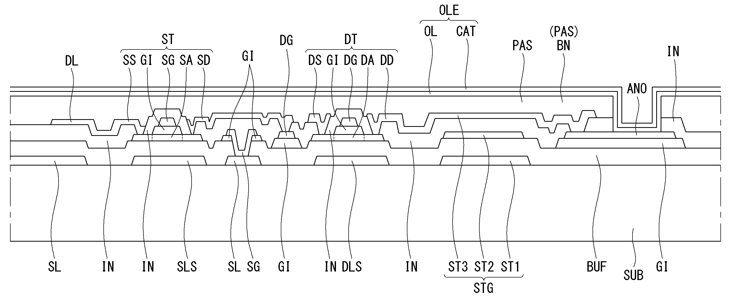
이하, 도 5 및 6을 참조하여 본 발명의 일 실시 예를 설명한다. 도 5는 본 발명에 의한 유기발광 다이오드 표시장치에서 한 화소의 구조를 나타내는 평면도이다. 도 6은 도 5에서 절취선 II-II'로 자른 본 발명에 의한 유기발광 다이오드 표시장치의 구조를 나타내는 단면도이다.Hereinafter, an embodiment of the present invention will be described with reference to FIGS. 5 and 6. 5 is a plan view showing a structure of one pixel in an organic light emitting diode display according to the present invention. 6 is a cross-sectional view showing the structure of an organic light emitting diode display according to the present invention, taken along a line II-II' in FIG. 5.
본 발명의 일 실시 예에 의한 액티브 매트릭스 유기발광 다이오드 표시장치는 스위칭 박막 트랜지스터(ST), 스위칭 박막 트랜지스터(ST)와 연결된 구동 박막 트랜지스터(DT), 구동 박막 트랜지스터(DT)에 접속된 유기발광 다이오드(OLE)를 포함한다. 스위칭 박막 트랜지스터(ST)는 스캔 배선(SL)과 데이터 배선(DL)이 교차하는 부위에 형성되어 있다. 스위칭 박막 트랜지스터(ST)는 화소를 선택하는 기능을 한다. 스위칭 박막 트랜지스터(ST)는 스캔 배선(SL)에서 분기하는 게이트 전극(SG)과, 반도체 층(SA)과, 소스 전극(SS)과, 드레인 전극(SD)을 포함한다.The active matrix organic light emitting diode display according to an embodiment of the present invention includes a switching thin film transistor ST, a driving thin film transistor DT connected to the switching thin film transistor ST, and an organic light emitting diode connected to the driving thin film transistor DT. (OLE) included. The switching thin film transistor ST is formed at a portion where the scan line SL and the data line DL cross each other. The switching thin film transistor ST serves to select a pixel. The switching thin film transistor ST includes a gate electrode SG branching from the scan line SL, a semiconductor layer SA, a source electrode SS, and a drain electrode SD.
그리고 구동 박막 트랜지스터(DT)는 스위칭 박막 트랜지스터(ST)에 의해 선택된 화소의 유기발광 다이오드(OLE)를 구동하는 역할을 한다. 구동 박막 트랜지스터(DT)는 스위칭 박막 트랜지스터(ST)의 드레인 전극(SD)과 연결된 게이트 전극(DG)과, 반도체 층(DA), 구동 전류 배선(VDD)에 연결된 소스 전극(DS)과, 드레인 전극(DD)을 포함한다. 구동 TFT(DT)의 드레인 전극(DD)은 유기발광 다이오드(OLE)의 애노드 전극(ANO)과 연결되어 있다.Further, the driving thin film transistor DT serves to drive the organic light emitting diode OLE of a pixel selected by the switching thin film transistor ST. The driving thin film transistor DT includes a gate electrode DG connected to the drain electrode SD of the switching thin film transistor ST, a semiconductor layer DA, a source electrode DS connected to the driving current line VDD, and a drain. It includes an electrode DD. The drain electrode DD of the driving TFT DT is connected to the anode electrode ANO of the organic light emitting diode OLE.
본 발명에서는, 고속 특성에 유리한 산화물 반도체 물질을 반도체 층(SA, DA)으로 사용하며, 탑 게이트 구조의 박막 트랜지스터(ST, DT)를 적용한다. 또한, 탑 게이트 구조의 박막 트랜지스터(ST, DT)를 하부 발광형 유기발광 다이오드 표시장치에 적용할 경우, 외부 광에 노출되는 반도체 층(SA, DA)을 보호하기 위해 차광층(SLS, DLS)을 더 구비한다.In the present invention, an oxide semiconductor material advantageous for high speed characteristics is used as the semiconductor layers SA and DA, and thin film transistors ST and DT having a top gate structure are applied. In addition, when the thin film transistors (ST, DT) of the top gate structure are applied to the bottom-emitting type organic light emitting diode display, light blocking layers (SLS, DLS) are used to protect the semiconductor layers (SA, DA) exposed to external light. It has more.
특히, 차광층(SLS, DLS)과 함께, 스캔 배선(SL)을 형성하여 스캔 배선(SL)과 데이터 배선(DL) 사이에 절연막이 두 개 개재되도록 함으로써, 스캔 배선(SL)과 데이터 배선(DL) 사이의 기생 용량을 극소화하고, 절연 파괴에 의한 손상을 방지한다. 또한, 차광층(SLS, DLS)과 함께, 제1 보조 용량 전극(ST1)을 형성하면, 보조 용량의 크기를 더 확보할 수 있어, 보조 용량의 면적을 줄이고, 개구 영역을 늘일 수 있다.In particular, by forming the scan wiring SL together with the light blocking layers SLS and DLS so that two insulating films are interposed between the scan wiring SL and the data wiring DL, the scan wiring SL and the data wiring ( It minimizes parasitic capacitance between DL) and prevents damage due to insulation breakdown. In addition, if the first storage capacitor electrode ST1 is formed together with the light blocking layers SLS and DLS, the size of the storage capacitor can be further secured, thereby reducing the area of the storage capacitor and increasing the opening area.
상세히 설명하기 위해 도 6을 더 참조하면, 액티브 매트릭스 유기발광 다이오드 표시장치는, 투명 기판(SUB) 위에 불투명 금속 물질로 만든 스캔 배선(SL)을포함한다. 한편, 스위칭 박막 트랜지스터(ST) 및 구동 박막 트랜지스터(DT)가 형성될 위치에는 스위칭 차광층(SLS) 및 구동 차광층(DLS)이 형성되어 있다. 또한, 보조 용량(STG)이 형성될 위치에는 제1 보조 용량 전극(ST1)이 형성되어 있다.Referring further to FIG. 6 for detailed description, the active matrix organic light emitting diode display includes a scan line SL made of an opaque metal material on a transparent substrate SUB. Meanwhile, a switching light blocking layer SLS and a driving light blocking layer DLS are formed at positions where the switching thin film transistor ST and the driving thin film transistor DT are to be formed. In addition, a first storage capacitor electrode ST1 is formed at a location where the storage capacitor STG is to be formed.
스캔 배선(SL), 스위칭 차광층(SLS), 구동 차광층(DLS) 및 제1 보조 용량 전극(ST1) 위에는 버퍼 층(BUF)이 도포되어 기판(SUB) 전체 표면을 덮고 있다. 버퍼 층(BUF) 위에는 반도체 층이 형성되는데, 스위칭 박막 트랜지스터(ST)의 채널영역(SA)은 스위칭 차광층(SLS) 영역 내에 중첩하도록, 구동 박막 트랜지스터(DT)의 채널영역(DA)은 구동 차광층(DLS) 영역 내에 중첩하도록 배치되어 있다. 또한, 반도체 층과 동일한 물질로, 보조 용량(STG)이 형성될 위치에, 제1 보조 용량 전극(ST1)과 중첩하는 제2 보조 용량 전극(ST2)이 형성되어 있다. 제2 보조 용량 전극(ST2)은 섬 모양으로 플로팅(floating)되도록 형성할 수도 있고, 스위칭 박막 트랜지스터(ST)의 반도체 층과 연결될 수도 있다. 도 5에서는 제2 보조 용량 전극(ST2)이 스위칭 박막 트랜지스터(ST)의 반도체 층과 연결된, 특히 드레인 영역에서 연장된 구조로 나타내었다.A buffer layer BUF is applied on the scan line SL, the switching light blocking layer SLS, the driving light blocking layer DLS, and the first storage capacitor electrode ST1 to cover the entire surface of the substrate SUB. A semiconductor layer is formed on the buffer layer BUF, and the channel region DA of the driving thin film transistor DT is driven so that the channel region SA of the switching thin film transistor ST is overlapped within the switching light blocking layer SLS region. It is disposed so as to overlap in the light blocking layer DLS area. In addition, a second storage capacitor electrode ST2 overlapping the first storage capacitor electrode ST1 is formed of the same material as the semiconductor layer at a location where the storage capacitor STG is to be formed. The second storage capacitor electrode ST2 may be formed to be floating in an island shape or may be connected to the semiconductor layer of the switching thin film transistor ST. In FIG. 5, the second storage capacitor electrode ST2 is connected to the semiconductor layer of the switching thin film transistor ST, and in particular, is shown in a structure extending from the drain region.
스위칭 채널영역(SA) 및 구동 채널영역(DA)의 각 상부에는 게이트 절연막(GI)과 스위칭 게이트 전극(SG) 및 구동 게이트 전극(DG)이 형성되어 있다. 또한, 화소 영역에는 화소 전극 혹은 애노드 전극(ANO)이 형성된다. 화소 전극 혹은 애노드 전극(ANO)과 게이트 전극들(SG, DG)을 동시에 형성하므로, 본 발명에서는 투명 도전 물질로 형성한다. 이 경우, 스위칭 게이트 전극(SG)은 스캔 배선(SL)과 연결하여야 한다. 본 발명에서는, 버퍼층(BUF)을 관통하는 차광층 콘택홀(LH)을 통해 스위칭 게이트 전극(SG)과 스캔 배선(SL)이 연결된다. 게이트 전극 물질이 형성되는 위치에 게이트 절연막(GI)을 형성하는 경우, 차광층 콘택홀(LH)은 게이트 절연막(GI)과 버퍼층(BUF)을 관통하도록 형성할 수 있다.A gate insulating layer GI, a switching gate electrode SG, and a driving gate electrode DG are formed on each of the switching channel region SA and the driving channel region DA. In addition, a pixel electrode or an anode electrode ANO is formed in the pixel region. Since the pixel electrode or anode electrode ANO and the gate electrodes SG and DG are simultaneously formed, in the present invention, they are formed of a transparent conductive material. In this case, the switching gate electrode SG should be connected to the scan line SL. In the present invention, the switching gate electrode SG and the scan wiring SL are connected through the light blocking layer contact hole LH penetrating the buffer layer BUF. When the gate insulating layer GI is formed at a position where the gate electrode material is formed, the light blocking layer contact hole LH may be formed to penetrate the gate insulating layer GI and the buffer layer BUF.
게이트 전극들(SG, DG)과 애노드 전극(ANO) 위에는 중간 절연막(IN)이 기판(SUB) 전체 표면에 걸쳐 형성되어 있다. 중간 절연막(IN) 위에는 구리와 같은 전도성 물질로 형성한 데이터 배선(DL)과 구동 전류 배선(VDD)이 배치된다. 데이터 배선(DL) 및 구동 전류 배선(VDD)은 스캔 배선(SL)과 교차하는 구조를 가져, 화소 영역을 정의한다. 특히, 데이터 배선(DL) 및 구동 전류 배선(VDD)이 스캔 배선(SL)과 교차하는 부위에서, 버퍼층(BUF)과 중간 절연막(IN)이 적층되어 개재되므로, 두 배선 사이에서의 절연성이 우수하며, 기생 용량의 발생을 억제할 수 있다. 특히, 데이터 배선(DL)이 스캔 배선(SL)을 타고 넘어가는 부위에서 절연 파괴(break-down)에 의한 배선 단선 혹은 열화(burning)를 방지할 수 있다.An intermediate insulating layer IN is formed over the entire surface of the substrate SUB on the gate electrodes SG and DG and the anode electrode ANO. A data line DL and a driving current line VDD formed of a conductive material such as copper are disposed on the intermediate insulating layer IN. The data line DL and the driving current line VDD have a structure crossing the scan line SL, and define a pixel region. In particular, since the buffer layer BUF and the intermediate insulating film IN are stacked and interposed at a portion where the data wiring DL and the driving current wiring VDD cross the scan wiring SL, the insulation between the two wirings is excellent. And can suppress the occurrence of parasitic capacity. In particular, it is possible to prevent wiring disconnection or burning due to insulation breakdown at a portion where the data line DL passes through the scan line SL.
또한, 중간 절연막(IN) 위에는, 데이터 배선(DL)에서 분기하는 스위칭 소스 전극(SS) 그리고 스위칭 소스 전극(SS)과 대향하여 배치된 스위칭 드레인 전극(SD)이 형성됨으로써, 스위칭 박막 트랜지스터(ST)가 형성된다. 스위칭 소스 전극(SS)은 스위칭 소스 콘택홀(SSH)을 통해 스위칭 채널영역(SA)의 일측과 연결된다. 스위칭 드레인 전극(SD)은 스위칭 드레인 콘택홀(SDH)을 통해 스위칭 채널영역(SA)의 타측과 연결된다. 마찬가지로 구동 전류 배선(VDD)에서 분기하는 구동 소스 전극(DS) 그리고 구동 소스 전극(DS)과 대향하여 배치된 구동 드레인 전극(DD)이 형성됨으로써, 구동 박막 트랜지스터(DT)가 형성된다. 구동 소스 전극(DS)은 구동 소스 콘택홀(DSH)을 통해 구동 채널영역(DA)의 일측과 연결된다. 구동 드레인 전극(DD)은 구동 드레인 콘택홀(DDH)을 통해 구동 채널영역(DA)의 타측과 연결된다. 한편, 스위칭 드레인 전극(SD)은 게이트 콘택홀(GH)을 통해 구동 게이트 전극(DG)과 연결된다.In addition, the switching source electrode SS branching from the data line DL and the switching drain electrode SD disposed opposite the switching source electrode SS are formed on the intermediate insulating layer IN, thereby forming the switching thin film transistor ST. ) Is formed. The switching source electrode SS is connected to one side of the switching channel region SA through the switching source contact hole SSH. The switching drain electrode SD is connected to the other side of the switching channel region SA through the switching drain contact hole SDH. Similarly, the driving source electrode DS branching from the driving current line VDD and the driving drain electrode DD disposed opposite to the driving source electrode DS are formed, thereby forming the driving thin film transistor DT. The driving source electrode DS is connected to one side of the driving channel region DA through the driving source contact hole DSH. The driving drain electrode DD is connected to the other side of the driving channel region DA through the driving drain contact hole DTH. Meanwhile, the switching drain electrode SD is connected to the driving gate electrode DG through the gate contact hole GH.
소스-드레인 요소들이 형성된 기판(SUB) 전체 표면 위에는 보호막(PAS) 혹은 뱅크(BN)이 도포되어 있다. 다른 예로, 보호막(PAS)과 뱅크(BA)가 순차적으로 적층된 구조를 가질 수도 있다. 보호막(PAS) 혹은 뱅크(BN) 그리고 애노드 전극(ANO)을 덮는 중간 절연막(IN)에는 애노드 전극(ANO)에서 발광 영역을 정의하는 개구부가 형성되어 있다.A passivation layer PAS or bank BN is applied on the entire surface of the substrate SUB on which the source-drain elements are formed. As another example, the passivation layer PAS and the bank BA may be sequentially stacked. An opening defining a light emitting area in the anode electrode ANO is formed in the passivation layer PAS or the intermediate insulating layer IN covering the bank BN and the anode electrode ANO.
유기발광 다이오드 표시장치의 경우, 뱅크(BN)가 형성된 기판(SUB)에서 애노드 전극(ANO) 위에 유기발광 층(OL)과 캐소드 전극(CAT)이 순차적으로 적층된다. 즉, 애노드 전극(ANO), 유기발광 층(OL) 및 캐소드 전극(CAT)의 적층구조로 유기발광 다이오드(OLE)가 구동 박막 트랜지스터(DT)에 연결되어 있다.In the case of an organic light emitting diode display, an organic light emitting layer OL and a cathode electrode CAT are sequentially stacked on an anode electrode ANO in a substrate SUB on which banks BN are formed. That is, the organic light emitting diode OLE is connected to the driving thin film transistor DT by a stacked structure of the anode electrode ANO, the organic light emitting layer OL, and the cathode electrode CAT.
본 발명의 설명에서, 칼라 필터에 대한 언급을 하지 않았다. 칼라 필터를 사용하면서 하부 발광형으로 구성할 경우, 애노드 전극(ANO) 하부에 칼라 필터를 형성하는 것이 바람직하다. 상부 발광형으로 구성할 경우에는, 애노드 전극(ANO) 위에 형성하는 것이 바람직하다. 경우에 따라서는, 유기발광 층(OL)이 적, 녹, 청 중 어느 하나를 발현하는 발광 물질을 사용하고, 각 화소 영역에 독립적으로 배치함으로써 칼라 필터를 적용하지 않는 구조를 가질 수도 있다.In the description of the present invention, no reference is made to the color filter. In the case of a bottom emission type while using a color filter, it is preferable to form a color filter under the anode electrode ANO. In the case of a top emission type, it is preferable to form on the anode electrode ANO. In some cases, the organic light-emitting layer OL may have a structure in which a color filter is not applied by using a light-emitting material that expresses any one of red, green, and blue, and is independently disposed in each pixel area.
본 발명의 일 실시 예를 설명하는 도 5에서는 스위칭 차광층(SLS)과 구동 차광층(DLS)이 섬 모양으로 독립된 형태로 도시하였다. 하지만, 필요하다면, 게이트 전극들(SG, DG)과 연결하여 이중 게이트 구조를 가질 수도 있다. 예를 들어, 스위칭 차광층(SLS)은 스캔 배선(SL)에서 연장되는 형태로 형성할 수 있다. 반면에 구동 차광층(DLS)은 구동 게이트 전극(DG)과 별도의 콘택홀(도시하지 않음)을 통해 연결될 수 있다.
In FIG. 5 for explaining an embodiment of the present invention, the switching light-shielding layer SLS and the driving light-shielding layer DLS are illustrated in an island shape in separate forms. However, if necessary, it may be connected to the gate electrodes SG and DG to have a double gate structure. For example, the switching light blocking layer SLS may be formed to extend from the scan line SL. On the other hand, the driving light blocking layer DLS may be connected to the driving gate electrode DG through a separate contact hole (not shown).
이하, 도 7a 내지 7g 그리고 도 8을 참조하여 본 발명에 의한 유기발광 다이오드 표시장치의 제조 방법을 설명한다. 도 7a 내지 7g는, 도 5에서 절취선 II-II'로 자른, 본 발명에 의한 유기발광 다이오드 표시장치의 제조 방법을 나타내는 단면도들이다. 도 8은 본 발명에 의한 유기발광 다이오드 표시장치의 제조 공정을 개략적으로 나타낸 흐름도이다.Hereinafter, a method of manufacturing an organic light emitting diode display according to the present invention will be described with reference to FIGS. 7A to 7G and FIG. 8. 7A to 7G are cross-sectional views illustrating a method of manufacturing an organic light-emitting diode display device according to the present invention, taken along a line II-II' in FIG. 5. 8 is a flowchart schematically illustrating a manufacturing process of an organic light emitting diode display according to the present invention.
먼저, 기판(SUB) 위에 불투명하고, 전도성이 우수한 금속 물질을 도포한다. 제1 마스크 공정으로 금속 물질을 패턴하여, 스캔 배선(SL), 차광층(SLS, DLS) 및 제1 보조 용량 전극(ST1)을 형성한다.(도 8의 S100) 스캔 배선(SL)은 기판(SUB)의 일축 방향으로 진행하도록 배치한다. 차광층은 나중에 형성될 박막 트랜지스터의 반도체 층 특히, 채널 영역과 중첩하도록 배치하는 것이 바람직하다. 예를 들어, 스위칭 차광층(SLS)는 스위칭 박막 트랜지스터(ST)가 형성될 위치에, 구동 차광층(DLS)는 구동 박막 트랜지스터(ST)가 형성될 위치에 배치한다. 또한, 보조 용량(STG)을 형성할 위치에는 제1 보조 용량 전극(ST1)을 형성한다. (도 7a)First, an opaque metal material having excellent conductivity is applied on the substrate SUB. The metal material is patterned by a first mask process to form the scan line SL, the light blocking layers SLS and DLS, and the first storage capacitor electrode ST1 (S100 in FIG. 8). The scan line SL is a substrate. Arrange to proceed in the uniaxial direction of (SUB). It is preferable to arrange the light shielding layer so as to overlap with the semiconductor layer of the thin film transistor to be formed later, in particular, the channel region. For example, the switching light blocking layer SLS is disposed at a position where the switching thin film transistor ST is to be formed, and the driving light blocking layer DLS is disposed at a position where the driving thin film transistor ST is formed. In addition, a first storage capacitor electrode ST1 is formed at a position where the storage capacitor STG is to be formed. (Fig. 7a)
스캔 배선(SL), 차광층(SLS, DLS) 및 제1 보조 용량 전극(ST1)이 형성된 기판(SUB)의 전체 표면 위에 버퍼층(BUF)을 도포한다. 순차적으로 버퍼층(BUF) 위에, 인듐-갈륨-아연-산화물(Indium-Galium-Zinc-Oxide: IGZO)과 같은 금속 산화물 반도체 물질을 도포한다. 제2 마스크 고정으로 산화물 반도체 물질을 패턴하여 반도체 층(SE)과 제2 보조 용량 전극(ST2)을 형성한다. (도 8의 S200) 반도체 층(SE)은 스위칭 박막 트랜지스터(ST)와 구동 박막 트랜지스터(DT)가 형성될 위치에 형성하는 것이 바람직하다. 제2 보조 용량 전극(ST2)은 제1 보조 용량 전극(ST1)과 중첩하도록 배치하는 것이 바람직하다. 특히, 제2 보조 용량 전극(ST2)은 스위칭 박막 트랜지스터(ST)에 배치된 반도체 층에서 연장되도록 형성할 수도 있다. (도 7b)The buffer layer BUF is applied on the entire surface of the substrate SUB on which the scan wiring SL, the light blocking layers SLS and DLS, and the first storage capacitor electrode ST1 are formed. A metal oxide semiconductor material such as Indium-Galium-Zinc-Oxide (IGZO) is sequentially coated on the buffer layer BUF. The oxide semiconductor material is patterned by fixing the second mask to form the semiconductor layer SE and the second storage capacitor electrode ST2. (S200 of FIG. 8) The semiconductor layer SE is preferably formed at a position where the switching thin film transistor ST and the driving thin film transistor DT are to be formed. It is preferable to arrange the second storage capacitor electrode ST2 to overlap the first storage capacitor electrode ST1. In particular, the second storage capacitor electrode ST2 may be formed to extend from the semiconductor layer disposed on the switching thin film transistor ST. (Fig. 7b)
반도체 층(SE)과 제2 보조 용량 전극(ST2)이 형성된 기판(SUB) 전체 표면 위에 절연물질을 도포한다. 제3 마스크 공정으로 절연 물질을 패턴하여, 게이트 절연막(GI)을 형성한다. 특히, 게이트 절연막(GI)은 반도체 층(SE)의 중앙부를 덮고 양측부를 노출하도록 형성한다. 이 과정에서 노출된 반도체 층(SE)의 양측부는 도체화된다. 반면에, 중앙부는 반도체 상태로 남아 채널 영역으로 정의된다. 즉, 스위칭 박막 트랜지스터(ST) 위치에는 스위칭 채널 영역(SA)이, 구동 박막 트랜지스터(DT) 위치에는 구동 채널 영역(DA)이 정의된다. 이때, 제2 보조 용량 전극(ST2) 위에도 절연물질을 제거하여, 도체화하는 것이 바람직하다. 게이트 절연막(GI) 위에 형성되는 게이트 전극이 스캔 배선(SL)과 연결될 수 있도록 하기 위해, 스캔 배선(SL)의 일부를 노출하는 차광층 콘택홀(LH)을 형성한다. (도 8의 300) 유사한 성질을 갖는 게이트 절연막(GI)과 버퍼층(BUF)을 동시에 패턴하기 위해, 필요하다면 하프-톤 마스크를 사용하는 것이 바람직하다. (도 7c)An insulating material is coated on the entire surface of the substrate SUB on which the semiconductor layer SE and the second storage capacitor electrode ST2 are formed. An insulating material is patterned by a third mask process to form a gate insulating layer GI. In particular, the gate insulating layer GI is formed to cover the central portion of the semiconductor layer SE and expose both side portions. In this process, both sides of the exposed semiconductor layer SE are conductive. On the other hand, the central portion remains in a semiconductor state and is defined as a channel region. That is, the switching channel region SA is defined at the position of the switching thin film transistor ST, and the driving channel region DA is defined at the position of the driving thin film transistor DT. In this case, it is preferable to remove the insulating material on the second storage capacitor electrode ST2 to form a conductor. In order to allow the gate electrode formed on the gate insulating layer GI to be connected to the scan line SL, a light blocking layer contact hole LH exposing a part of the scan line SL is formed. (300 in FIG. 8) In order to simultaneously pattern the gate insulating film GI and the buffer layer BUF having similar properties, it is preferable to use a half-tone mask if necessary. (Fig. 7c)
게이트 절연막(GI)이 형성된 기판(SUB) 전체 표면 위에 인듐-주석-산화물(Indium-Tin-Oxide: ITO)와 같은 투명 도전 물질을 도포한다. 제4 마스크 공정으로 투명 도전 물질을 패턴하여, 게이트 전극(SG, DG) 및 애노드 전극(ANO)을 형성한다. (도 8의 400) 스위칭 게이트 전극(SG)은 스위칭 채널 영역(SA)을 정의하는 게이트 절연막(GI) 위에 형성하는 것이 바람직하다. 마찬가지로 구동 게이트 전극(DG)은 구동 채널 영역(DA)을 정의하는 게이트 절연막(GI) 위에 형성하는 것이 바람직하다. 한편, 스위칭 게이트 전극(SG)은 스캔 배선(SL)과 중첩하도록 연장되어, 차광층 콘택홀(LH)을 통해 스캔 배선(SL)과 접촉한다. 또한, 화소 영역 내에는 애노드 전극(ANO)을 형성한다. 투명 도전 물질을 이용하여, 애노드 전극(ANO)과 게이트 전극들(SG, DG)을 동시에 형성함으로써, 마스크 공정 수를 절감할 수 있다. (도 7d)A transparent conductive material such as Indium-Tin-Oxide (ITO) is coated on the entire surface of the substrate SUB on which the gate insulating layer GI is formed. A transparent conductive material is patterned by a fourth mask process to form gate electrodes SG and DG and anode electrodes ANO. (400 of FIG. 8) The switching gate electrode SG is preferably formed on the gate insulating film GI defining the switching channel region SA. Similarly, the driving gate electrode DG is preferably formed on the gate insulating film GI defining the driving channel region DA. Meanwhile, the switching gate electrode SG extends to overlap the scan line SL and contacts the scan line SL through the light blocking layer contact hole LH. In addition, an anode electrode ANO is formed in the pixel area. By simultaneously forming the anode electrode ANO and the gate electrodes SG and DG using a transparent conductive material, it is possible to reduce the number of mask processes. (Fig. 7d)
투명 도전층 요소들이 형성된 기판(SUB) 전체 표면 위에 절연 물질을 도포하여 중간 절연막(IN)을 형성한다. 제5 마스크 공정으로 중간 절연막(IN)을 패턴하여, 필요한 콘택홀들을 형성한다. (도 8의 500) 예를 들어, 스위칭 채널영역(SA)의 양측부 도체화 영역을 노출하는 스위칭 소스 콘택홀(SSH)과 스위칭 드레인 콘택홀(SDH)을 형성한다. 마찬가지로, 구동 채널 영역(DA)의 양측부 도체화 영역을 노출하는 구동 소스 콘택홀(DSH)과 구동 드레인 콘택홀(DDH)을 형성한다. 또한, 구동 게이트 전극(DG)의 일부를 노출하는 게이트 콘택홀(GH)을 형성한다. (도 7e)The intermediate insulating layer IN is formed by applying an insulating material on the entire surface of the substrate SUB on which the transparent conductive layer elements are formed. The intermediate insulating layer IN is patterned by a fifth mask process to form necessary contact holes. (500 of FIG. 8) For example, a switching source contact hole SSH and a switching drain contact hole SDH are formed exposing the conductive regions on both sides of the switching channel region SA. Similarly, a driving source contact hole DSH and a driving drain contact hole DTH exposing the conductive regions on both sides of the driving channel region DA are formed. Also, a gate contact hole GH exposing a part of the driving gate electrode DG is formed. (Fig. 7e)
콘택홀들이 형성된 기판(SUB) 전체 표면 위에 전도성이 우수한 금속 물질을 도포한다. 전도성이 우수한 금속 물질은 구리 혹은 알루미늄을 포함하는 것이 바람직하다. 필요하다면, 몰리브덴/구리/몰리브덴과 같이 3중 혹은 이중 금속이 적층된 구조를 가질 수도 있다. 제6 마스크 공정으로 금속 물질을 패턴하여 소스-드레인 요소를 형성한다. (도 8의 600) 소스-드레인 요소에는 기판(SUB)의 타측 방향으로 연장되는 데이터 배선(DL) 및 구동 전류 배선(VDD), 데이터 배선(DL)에서 분기하는 스위칭 소스 전극(SS) 및 구동 전류 배선(VDD)에서 분기하는 구동 소스 전극(DS) 그리고 스위칭 소스 전극(SS)과 대향하는 스위칭 드레인 전극(SD) 및 구동 소스 전극(DS)과 대향하는 구동 드레인 전극(DD)을 포함한다.A metal material having excellent conductivity is coated on the entire surface of the substrate SUB in which the contact holes are formed. It is preferable that the metal material having excellent conductivity includes copper or aluminum. If necessary, it may have a structure in which triple or double metals are laminated, such as molybdenum/copper/molybdenum. A source-drain element is formed by patterning a metal material in a sixth mask process. (600 of FIG. 8) In the source-drain element, a data line DL and a driving current line VDD extending in the other direction of the substrate SUB, a switching source electrode SS branching from the data line DL, and driving A driving source electrode DS branching from the current line VDD, a switching drain electrode SD facing the switching source electrode SS, and a driving drain electrode DD facing the driving source electrode DS.
스위칭 소스 전극(SS)은 스위칭 소스 콘택홀(SSH)을 통해 스위칭 채널 영역(SA)의 일측부와 연결된다. 스위칭 드레인 전극(SD)은 스위칭 드레인 콘택홀(SDH)을 통해 스위칭 채널 영역(SA)의 타측부와 연결된다. 마찬가지로, 구동 소스 전극(DS)은 구동 소스 콘택홀(DSH)을 통해 구동 채널 영역(DA)의 일측부와 연결된다. 구동 드레인 전극(DD)은 구동 드레인 콘택홀(DDH)을 통해 구동 채널 영역(DA)의 타측부와 연결된다. (도 7f)The switching source electrode SS is connected to one side of the switching channel region SA through the switching source contact hole SSH. The switching drain electrode SD is connected to the other side of the switching channel region SA through the switching drain contact hole SDH. Likewise, the driving source electrode DS is connected to one side of the driving channel area DA through the driving source contact hole DSH. The driving drain electrode DD is connected to the other side of the driving channel region DA through the driving drain contact hole DTH. (Fig. 7f)
소스-드레인 요소들이 형성된 기판(SUB) 전체 표면 위에 절연 물질을 도포한다. 여기서, 절연 물질은 무기 절연 물질 혹은 유기 절연 물질을 포함할 수 있다. 경우에 따라서는, 무기 절연 물질과 유기 절연 물질을 순차적으로 적층할 수도 있다. 유기발광 다이오드 표시장치의 경우에는, 감광성 유기 절연 물질을 도포할 수 있다. 제7 마스크 공정으로 절연 물질을 패턴하여 애노드 전극(ANO)의 대부분을 노출하는 개구부를 정의하는 뱅크(BN)을 형성한다. (도 8의 700) (도 7g)An insulating material is applied over the entire surface of the substrate SUB on which the source-drain elements are formed. Here, the insulating material may include an inorganic insulating material or an organic insulating material. In some cases, an inorganic insulating material and an organic insulating material may be sequentially stacked. In the case of an organic light emitting diode display, a photosensitive organic insulating material may be applied. An insulating material is patterned in the seventh mask process to form banks BN defining openings exposing most of the anode electrode ANO. (700 in Fig. 8) (Fig. 7g)
이후, 도면으로 도시하지 않았지만, 뱅크(BN)가 형성된 기판(SUB) 전체 표면 위에 유기발광 층(OL)과 캐소드 전극(CAT)을 순차적으로 도포하면, 도 6과 같은 구조를 갖는 유기발광 다이오드 표시장치를 완성할 수 있다. 여기서는 박막 트랜지스터 기판을 제조하는 과정을 중심으로 설명하였다.
Thereafter, although not shown in the drawing, when the organic light emitting layer OL and the cathode electrode CAT are sequentially applied on the entire surface of the substrate SUB on which the banks BN are formed, the organic light emitting diode display having the structure as shown in FIG. 6 You can complete the device. Here, the process of manufacturing the thin film transistor substrate has been mainly described.
이상 설명한 내용을 통해 당업자라면 본 발명의 기술 사상을 일탈하지 아니하는 범위 내에서 다양한 변경 및 수정이 가능함을 알 수 있을 것이다. 따라서, 본 발명은 상세한 설명에 기재된 내용으로 한정되는 것이 아니라 특허 청구 범위에 의해 정해져야만 할 것이다.It will be appreciated by those skilled in the art through the above description that various changes and modifications can be made without departing from the spirit of the present invention. Accordingly, the present invention should not be limited to the content described in the detailed description, but should be defined by the claims.
DL: 데이터 배선 SL: 스캔 배선
VDD: 구동 전류 배선 ST: 스위칭 TFT
DT: 구동 TFT OLED: 유기발광 다이오드
CAT: 캐소드 전극(층) ANO: 애노드 전극(층)
BN: 뱅크 CF: 칼라 필터
OLE: (백색) 유기발광 층 SUB: 기판
PAS: 보호막 OC: 오버코트 층
SG, DG: 게이트 전극 SE: 반도체 층
SS, DS: 소스 전극 SD, DD: 드레인 전극
BUF: 버퍼층 PH: 화소 콘택홀
SLS: 스위칭 차광층 DLS: 구동 차광층
STG: 보조 용량 SG1: 제1 보조 용량 전극
SG2: 제2 보조 용량 전극 SG3: 제3 보조 용량 전극DL: Data wiring SL: Scan wiring
VDD: drive current wiring ST: switching TFT
DT: Driving TFT OLED: Organic Light-Emitting Diode
CAT: cathode electrode (layer) ANO: anode electrode (layer)
BN: Bank CF: Color filter
OLE: (white) organic light emitting layer SUB: substrate
PAS: protective film OC: overcoat layer
SG, DG: gate electrode SE: semiconductor layer
SS, DS: source electrode SD, DD: drain electrode
BUF: buffer layer PH: pixel contact hole
SLS: switching light-shielding layer DLS: driving light-shielding layer
STG: storage capacitor SG1: first storage capacitor electrode
SG2: second storage capacitor electrode SG3: third storage capacitor electrode
Claims (5)
상기 기판 위에서 상기 화소 영역의 일측 방향으로 배치된 스캔 배선;
상기 스캔 배선을 덮는 버퍼층;
상기 버퍼층 위에 배치된 반도체 층;
상기 반도체 층의 중앙 영역인 채널 영역을 덮는 게이트 절연막;
상기 게이트 절연막 위에서 상기 채널 영역과 중첩하고, 상기 스캔 배선과 연결된 게이트 전극;
상기 게이트 절연막 위에서 상기 화소 영역 내에 배치된 애노드 전극;
상기 게이트 전극을 덮으며, 상기 애노드 전극의 중앙 대부분을 노출하는 중간 절연막; 그리고
상기 중간 절연막 위에서 상기 화소 영역의 타측 방향으로 배치된 데이터 배선을 포함하는 박막 트랜지스터 기판.
A substrate on which a plurality of pixel regions are defined;
A scan line disposed on the substrate in a direction of one side of the pixel area;
A buffer layer covering the scan wiring;
A semiconductor layer disposed on the buffer layer;
A gate insulating layer covering a channel region that is a central region of the semiconductor layer;
A gate electrode overlapping the channel region on the gate insulating layer and connected to the scan line;
An anode electrode disposed in the pixel area on the gate insulating layer;
An intermediate insulating layer covering the gate electrode and exposing most of the center of the anode electrode; And
A thin film transistor substrate comprising a data line disposed on the intermediate insulating layer in a direction to the other side of the pixel region.
상기 스캔 배선과 동일한 물질을 포함하며, 동일한 층에서 상기 반도체 층과 중첩하도록 배치되는 차광층 및 보조 용량의 위치에 배치되는 제1 보조 용량 전극;
상기 반도체 층과 동일한 물질을 포함하며, 동일한 층에서 상기 보조 용량의 위치에 배치되는 제2 보조 용량 전극; 그리고
상기 데이터 배선과 동일한 물질을 포함하며, 동일한 층에서 상기 데이터 배선에서 분기되어 상기 반도체 층의 일측부와 접촉하는 소스 전극, 상기 소스 전극과 일정 거리 이격하여 배치되어 상기 반도체 층의 타측부와 접촉하는 드레인 전극 및 상기 드레인 전극에서 연장되어 상기 제2 보조 용량 전극과 중첩하는 제3 보조 용량 전극을 더 포함하는 박막 트랜지스터 기판.
The method of claim 1,
A first storage capacitor electrode that includes the same material as the scan wiring and is disposed at a position of a light blocking layer and an auxiliary capacitor disposed to overlap the semiconductor layer in the same layer;
A second storage capacitor electrode comprising the same material as the semiconductor layer and disposed at a position of the storage capacitor in the same layer; And
A source electrode comprising the same material as the data line, branching from the data line on the same layer and contacting one side of the semiconductor layer, and a predetermined distance apart from the source electrode to contact the other side of the semiconductor layer. A thin film transistor substrate further comprising a drain electrode and a third storage capacitor electrode extending from the drain electrode and overlapping the second storage capacitor electrode.
상기 데이터 배선을 덮으며, 상기 애노드 전극의 중앙부 대부분을 노출하는 개구 영역을 정의하는 뱅크;
상기 뱅크 위에서 상기 노출된 애노드 전극 위에 적층된 유기발광 층; 그리고
상기 유기발광 층 위에 적층된 캐소드 전극을 더 포함하는 박막 트랜지스터 기판.
The method of claim 1,
A bank covering the data line and defining an opening area exposing most of the central portion of the anode electrode;
An organic light emitting layer stacked on the exposed anode electrode on the bank; And
A thin film transistor substrate further comprising a cathode electrode stacked on the organic emission layer.
상기 게이트 전극 및 상기 애노드 전극은 동일한 층에 배치되며, 인듐-주석-산화물과 같은 투명 도전 물질을 포함하는 박막 트랜지스터 기판.
The method of claim 1,
The gate electrode and the anode electrode are disposed on the same layer and include a transparent conductive material such as indium-tin-oxide.
상기 스캔 배선이 형성된 상기 기판 표면 위에 버퍼층을 도포하고, 상기 버퍼층 위에 반도체 층을 형성하는 단계;
상기 반도체 층의 중앙부 및 화소 영역을 덮는 게이트 절연막을 형성하는 단계;
상기 게이트 절연막 위에서 상기 반도체 층의 상기 중앙부와 중첩하는 게이트 전극 및 상기 화소 영역에 배치된 애노드 전극을 형성하는 단계;
상기 게이트 전극 및 상기 애노드 전극을 덮는 중간 절연막을 형성하는 단계;
상기 중간 절연막 위에서 상기 스캔 배선과 교차하는 데이터 배선을 형성하는 단계; 그리고
상기 데이터 배선을 덮으며 상기 애노드 전극의 중앙부 대부분을 노출하는 뱅크를 형성하는 단계를 포함하는 박막 트랜지스터 기판 제조 방법.Forming scan wirings on the substrate;
Applying a buffer layer on the surface of the substrate on which the scan wiring is formed, and forming a semiconductor layer on the buffer layer;
Forming a gate insulating layer covering a central portion and a pixel region of the semiconductor layer;
Forming a gate electrode overlapping the central portion of the semiconductor layer and an anode electrode disposed in the pixel region on the gate insulating layer;
Forming an intermediate insulating layer covering the gate electrode and the anode electrode;
Forming a data line crossing the scan line on the intermediate insulating layer; And
And forming a bank covering the data line and exposing most of the central portion of the anode electrode.
Priority Applications (1)
| Application Number | Priority Date | Filing Date | Title |
|---|---|---|---|
| KR1020140132060A KR102211066B1 (en) | 2014-09-30 | 2014-09-30 | Thin film Transistor Substrate For Flat Panel Display And Method For Manufacturing The Same |
Applications Claiming Priority (1)
| Application Number | Priority Date | Filing Date | Title |
|---|---|---|---|
| KR1020140132060A KR102211066B1 (en) | 2014-09-30 | 2014-09-30 | Thin film Transistor Substrate For Flat Panel Display And Method For Manufacturing The Same |
Publications (2)
| Publication Number | Publication Date |
|---|---|
| KR20160039092A KR20160039092A (en) | 2016-04-08 |
| KR102211066B1 true KR102211066B1 (en) | 2021-02-03 |
Family
ID=55907942
Family Applications (1)
| Application Number | Title | Priority Date | Filing Date |
|---|---|---|---|
| KR1020140132060A Active KR102211066B1 (en) | 2014-09-30 | 2014-09-30 | Thin film Transistor Substrate For Flat Panel Display And Method For Manufacturing The Same |
Country Status (1)
| Country | Link |
|---|---|
| KR (1) | KR102211066B1 (en) |
Families Citing this family (5)
| Publication number | Priority date | Publication date | Assignee | Title |
|---|---|---|---|---|
| KR102554862B1 (en) * | 2016-11-21 | 2023-07-14 | 삼성디스플레이 주식회사 | Display device |
| KR102092034B1 (en) | 2017-12-06 | 2020-03-23 | 엘지디스플레이 주식회사 | Display device and method of manufacturing the same |
| KR102741523B1 (en) * | 2018-10-24 | 2024-12-11 | 삼성디스플레이 주식회사 | Organic light emitting diode display device |
| US11581340B2 (en) * | 2020-12-15 | 2023-02-14 | Sharp Kabushiki Kaisha | Active matrix substrate |
| US12219827B2 (en) * | 2021-08-25 | 2025-02-04 | Hefei Boe Joint Technology Co., Ltd. | Display substrate and display device |
Family Cites Families (3)
| Publication number | Priority date | Publication date | Assignee | Title |
|---|---|---|---|---|
| KR20110038931A (en) * | 2009-10-09 | 2011-04-15 | 엘지디스플레이 주식회사 | Display device and manufacturing method |
| KR101991338B1 (en) * | 2012-09-24 | 2019-06-20 | 엘지디스플레이 주식회사 | Thin film transistor array substrate and method for manufacturing of the same |
| KR102024784B1 (en) * | 2012-12-18 | 2019-09-24 | 엘지디스플레이 주식회사 | Organic Light Emitting Diode Display And Method For Manufacturing The Same |
-
2014
- 2014-09-30 KR KR1020140132060A patent/KR102211066B1/en active Active
Also Published As
| Publication number | Publication date |
|---|---|
| KR20160039092A (en) | 2016-04-08 |
Similar Documents
| Publication | Publication Date | Title |
|---|---|---|
| KR102482991B1 (en) | Top Emission Type Organic Light Emitting Diode Display | |
| KR102482990B1 (en) | Top Emission Type Organic Light Emitting Diode Display | |
| KR102045036B1 (en) | Organic Light Emitting Diode Display Having High Aperture Ratio And Method For Manufacturing The Same | |
| KR102315094B1 (en) | Organic Light Emitting Diode Display Having High Aperture Ratio And Method For Manufacturing The Same | |
| KR102158771B1 (en) | Organic light emitting diode display | |
| KR102062912B1 (en) | Organic Light Emitting Diode Display And Method For Manufacturing The Same | |
| KR102166341B1 (en) | Organic Light Emitting Diode Display Having High Aperture Ratio And Method For Manufacturing The Same | |
| KR102130139B1 (en) | Organic Light Emitting Diode Display Having Thin Film Transistor Substrate Using Oxide Semiconductor And Method For Manufacturing The Same | |
| KR102556162B1 (en) | Thin film Transistor Substrate For Flat Panel Display | |
| KR102193886B1 (en) | Organic Light Emitting Diode Display Having High Aperture Ratio And Method For Manufacturing The Same | |
| US9941338B2 (en) | Organic light-emitting diode display and method of manufacturing the same | |
| KR20190042395A (en) | Large Area Organic Light Emitting Diode Display | |
| KR102076620B1 (en) | Organic Light Emitting Diode Display And Method For Manufacturing The Same | |
| KR102519942B1 (en) | Thin Film Transistor Substrate For Organic Light Emitting Diode Display | |
| KR101746841B1 (en) | Organic light emitting diode display device and manufacturing method of the same | |
| US20120050235A1 (en) | Organic electroluminescence emitting display and method of manufacturing the same | |
| US11574975B2 (en) | Light emitting diode display device with channel region covered by drain electrode | |
| KR102211066B1 (en) | Thin film Transistor Substrate For Flat Panel Display And Method For Manufacturing The Same | |
| US11233108B2 (en) | Display device | |
| KR102247825B1 (en) | Bottom Emission Type Organic Light Emission Diode Display Having Color Filters And Method For Manufacturing The Same | |
| KR102269099B1 (en) | Thin film Transistor Substrate For Flat Panel Display And Method For Manufacturing The Same | |
| KR102053440B1 (en) | Organic Light Emitting Diode Display Having High Aperture Ratio And Method For Manufacturing The Same | |
| KR102056275B1 (en) | Ultra High Density Organic Light Emitting Diode Display | |
| KR102268516B1 (en) | Thin Film Transistor Substrate For Ultra High Density Flat Panel Display And Method For Manufacturing The Same | |
| KR102135916B1 (en) | Thin Film Transistor Substrate For Ultra High Density Flat Panel Display |
Legal Events
| Date | Code | Title | Description |
|---|---|---|---|
| PA0109 | Patent application |
St.27 status event code: A-0-1-A10-A12-nap-PA0109 |
|
| PG1501 | Laying open of application |
St.27 status event code: A-1-1-Q10-Q12-nap-PG1501 |
|
| P22-X000 | Classification modified |
St.27 status event code: A-2-2-P10-P22-nap-X000 |
|
| A201 | Request for examination | ||
| PA0201 | Request for examination |
St.27 status event code: A-1-2-D10-D11-exm-PA0201 |
|
| R17-X000 | Change to representative recorded |
St.27 status event code: A-3-3-R10-R17-oth-X000 |
|
| E902 | Notification of reason for refusal | ||
| PE0902 | Notice of grounds for rejection |
St.27 status event code: A-1-2-D10-D21-exm-PE0902 |
|
| P11-X000 | Amendment of application requested |
St.27 status event code: A-2-2-P10-P11-nap-X000 |
|
| P13-X000 | Application amended |
St.27 status event code: A-2-2-P10-P13-nap-X000 |
|
| E701 | Decision to grant or registration of patent right | ||
| PE0701 | Decision of registration |
St.27 status event code: A-1-2-D10-D22-exm-PE0701 |
|
| GRNT | Written decision to grant | ||
| PR0701 | Registration of establishment |
St.27 status event code: A-2-4-F10-F11-exm-PR0701 |
|
| PR1002 | Payment of registration fee |
St.27 status event code: A-2-2-U10-U11-oth-PR1002 Fee payment year number: 1 |
|
| PG1601 | Publication of registration |
St.27 status event code: A-4-4-Q10-Q13-nap-PG1601 |
|
| P22-X000 | Classification modified |
St.27 status event code: A-4-4-P10-P22-nap-X000 |
|
| PR1001 | Payment of annual fee |
St.27 status event code: A-4-4-U10-U11-oth-PR1001 Fee payment year number: 4 |
|
| P22-X000 | Classification modified |
St.27 status event code: A-4-4-P10-P22-nap-X000 |
|
| PR1001 | Payment of annual fee |
St.27 status event code: A-4-4-U10-U11-oth-PR1001 Fee payment year number: 5 |
|
| P22-X000 | Classification modified |
St.27 status event code: A-4-4-P10-P22-nap-X000 |