KR102190302B1 - Process kit for edge critical dimension uniformity control - Google Patents
Process kit for edge critical dimension uniformity control Download PDFInfo
- Publication number
- KR102190302B1 KR102190302B1 KR1020167000788A KR20167000788A KR102190302B1 KR 102190302 B1 KR102190302 B1 KR 102190302B1 KR 1020167000788 A KR1020167000788 A KR 1020167000788A KR 20167000788 A KR20167000788 A KR 20167000788A KR 102190302 B1 KR102190302 B1 KR 102190302B1
- Authority
- KR
- South Korea
- Prior art keywords
- ring
- top surface
- substrate
- ring assembly
- silicon
- Prior art date
- Legal status (The legal status is an assumption and is not a legal conclusion. Google has not performed a legal analysis and makes no representation as to the accuracy of the status listed.)
- Active
Links
Images


Classifications
-
- H—ELECTRICITY
- H01—ELECTRIC ELEMENTS
- H01J—ELECTRIC DISCHARGE TUBES OR DISCHARGE LAMPS
- H01J37/00—Discharge tubes with provision for introducing objects or material to be exposed to the discharge, e.g. for the purpose of examination or processing thereof
- H01J37/32—Gas-filled discharge tubes
- H01J37/32431—Constructional details of the reactor
- H01J37/32623—Mechanical discharge control means
- H01J37/32642—Focus rings
-
- H—ELECTRICITY
- H01—ELECTRIC ELEMENTS
- H01J—ELECTRIC DISCHARGE TUBES OR DISCHARGE LAMPS
- H01J37/00—Discharge tubes with provision for introducing objects or material to be exposed to the discharge, e.g. for the purpose of examination or processing thereof
- H01J37/32—Gas-filled discharge tubes
- H01J37/32431—Constructional details of the reactor
- H01J37/3244—Gas supply means
- H01J37/32449—Gas control, e.g. control of the gas flow
-
- H—ELECTRICITY
- H01—ELECTRIC ELEMENTS
- H01J—ELECTRIC DISCHARGE TUBES OR DISCHARGE LAMPS
- H01J37/00—Discharge tubes with provision for introducing objects or material to be exposed to the discharge, e.g. for the purpose of examination or processing thereof
- H01J37/32—Gas-filled discharge tubes
- H01J37/32431—Constructional details of the reactor
- H01J37/32623—Mechanical discharge control means
- H01J37/32651—Shields, e.g. dark space shields, Faraday shields
-
- H—ELECTRICITY
- H01—ELECTRIC ELEMENTS
- H01L—SEMICONDUCTOR DEVICES NOT COVERED BY CLASS H10
- H01L21/00—Processes or apparatus adapted for the manufacture or treatment of semiconductor or solid state devices or of parts thereof
- H01L21/02—Manufacture or treatment of semiconductor devices or of parts thereof
- H01L21/02104—Forming layers
- H01L21/02107—Forming insulating materials on a substrate
- H01L21/02296—Forming insulating materials on a substrate characterised by the treatment performed before or after the formation of the layer
- H01L21/02299—Forming insulating materials on a substrate characterised by the treatment performed before or after the formation of the layer pre-treatment
- H01L21/02312—Forming insulating materials on a substrate characterised by the treatment performed before or after the formation of the layer pre-treatment treatment by exposure to a gas or vapour
- H01L21/02315—Forming insulating materials on a substrate characterised by the treatment performed before or after the formation of the layer pre-treatment treatment by exposure to a gas or vapour treatment by exposure to a plasma
-
- H—ELECTRICITY
- H01—ELECTRIC ELEMENTS
- H01L—SEMICONDUCTOR DEVICES NOT COVERED BY CLASS H10
- H01L21/00—Processes or apparatus adapted for the manufacture or treatment of semiconductor or solid state devices or of parts thereof
- H01L21/02—Manufacture or treatment of semiconductor devices or of parts thereof
- H01L21/02104—Forming layers
- H01L21/02107—Forming insulating materials on a substrate
- H01L21/02296—Forming insulating materials on a substrate characterised by the treatment performed before or after the formation of the layer
- H01L21/02318—Forming insulating materials on a substrate characterised by the treatment performed before or after the formation of the layer post-treatment
- H01L21/02337—Forming insulating materials on a substrate characterised by the treatment performed before or after the formation of the layer post-treatment treatment by exposure to a gas or vapour
- H01L21/0234—Forming insulating materials on a substrate characterised by the treatment performed before or after the formation of the layer post-treatment treatment by exposure to a gas or vapour treatment by exposure to a plasma
-
- H—ELECTRICITY
- H01—ELECTRIC ELEMENTS
- H01L—SEMICONDUCTOR DEVICES NOT COVERED BY CLASS H10
- H01L21/00—Processes or apparatus adapted for the manufacture or treatment of semiconductor or solid state devices or of parts thereof
- H01L21/67—Apparatus specially adapted for handling semiconductor or electric solid state devices during manufacture or treatment thereof; Apparatus specially adapted for handling wafers during manufacture or treatment of semiconductor or electric solid state devices or components ; Apparatus not specifically provided for elsewhere
- H01L21/67005—Apparatus not specifically provided for elsewhere
- H01L21/67011—Apparatus for manufacture or treatment
- H01L21/67155—Apparatus for manufacturing or treating in a plurality of work-stations
- H01L21/67207—Apparatus for manufacturing or treating in a plurality of work-stations comprising a chamber adapted to a particular process
Landscapes
- Engineering & Computer Science (AREA)
- Physics & Mathematics (AREA)
- Plasma & Fusion (AREA)
- Chemical & Material Sciences (AREA)
- Analytical Chemistry (AREA)
- Power Engineering (AREA)
- Drying Of Semiconductors (AREA)
- General Physics & Mathematics (AREA)
- Condensed Matter Physics & Semiconductors (AREA)
- Manufacturing & Machinery (AREA)
- Computer Hardware Design (AREA)
- Microelectronics & Electronic Packaging (AREA)
- Plasma Technology (AREA)
- Ceramic Engineering (AREA)
Abstract
조정가능한 링 조립체, 조정가능한 링 조립체를 갖는 플라즈마 프로세싱 챔버, 및 플라즈마 프로세스를 조정하기 위한 방법이 제공된다. 일 실시예에서, 조정가능한 링 조립체는, 노출된 최상부 표면 및 바닥 표면을 갖는 외측 세라믹 링, 및 외측 세라믹 링과 정합하여 오버랩 영역을 정의하도록 구성되는 내측 실리콘 링을 포함하며, 내측 실리콘 링은, 내측 표면, 최상부 표면, 및 내측 표면과 최상부 표면 사이에 형성된 노치를 가지며, 내측 표면은 링 조립체의 내경을 정의하고, 노치는 기판의 엣지를 수용하는 크기로 만들어지며, 내측 실리콘 링의 최상부 표면의 외측 부분은 오버랩 영역에서 외측 세라믹 링의 바닥 표면의 내측 부분과 접촉하도록 구성되며 외측 세라믹 링의 바닥 표면의 내측 부분 아래에 놓인다.An adjustable ring assembly, a plasma processing chamber having an adjustable ring assembly, and a method for adjusting a plasma process are provided. In one embodiment, the adjustable ring assembly comprises an outer ceramic ring having an exposed top surface and a bottom surface, and an inner silicon ring configured to mate with the outer ceramic ring to define an overlap area, the inner silicon ring, It has an inner surface, a top surface, and a notch formed between the inner surface and the top surface, the inner surface defining the inner diameter of the ring assembly, and the notch is sized to accommodate the edge of the substrate, and the top surface of the inner silicon ring The outer portion is configured to contact an inner portion of the bottom surface of the outer ceramic ring in the overlap area and lies below the inner portion of the bottom surface of the outer ceramic ring.
Description
[0001] 본원의 실시예들은 일반적으로, 플라즈마 프로세싱 동안 기판의 엣지를 따라서 임계 치수들의 균일성을 제어하는 것에 관한 것이다. 보다 구체적으로, 이 실시예들은 조정가능한(tunable) 링 프로세스 키트 및 조정가능한 링 프로세스 키트를 사용하기 위한 방법에 관한 것이다.[0001] Embodiments herein generally relate to controlling the uniformity of critical dimensions along an edge of a substrate during plasma processing. More specifically, these embodiments relate to a tunable ring process kit and a method for using the tunable ring process kit.
[0002] 다양한 반도체 제조 프로세스들, 이를테면 특히, 플라즈마-보조 에칭, 물리 기상 증착, 및 화학 기상 증착이 플라즈마 프로세싱 챔버들에서 수행되며, 플라즈마 프로세싱 챔버들 내에서 반도체 워크피스가 프로세싱 동안 커버 링과 맞물린다. 예를 들면, 워크피스를 에칭하도록 구성된 플라즈마 프로세싱 챔버에서, 반도체 기판이 프로세싱 챔버 내의 기판 지지 페디스털 상에 장착된다. 기판 지지 페디스털은 RF 바이어스가 인가될 수 있는 금속 전극을 포함한다. 프로세싱 챔버에 제공되는 프로세스 가스들의 혼합물로부터 플라즈마가 형성된다. 프로세싱 챔버 내의 압력은 펌프에 의해 유지되며, 펌프는 또한 챔버로부터 부산물들을 제거한다. 전극 상에 플라즈마에 대한 네거티브 바이어스 전압(negative bias voltage)을 생성하도록, 기판 지지 페디스털 내의 전극에 전력 공급원(power supply)이 커플링된다. 바이어스 전압은 희망 제조 프로세스를 촉진시키기 위해, 워크피스에 충격을 주도록 플라즈마로부터 이온들을 끌어당긴다. 전극이 네거티브로 바이어싱되기 때문에, 기판 지지 페디스털은 종종 캐소드로 지칭된다.[0002] Various semiconductor manufacturing processes, such as, in particular, plasma-assisted etching, physical vapor deposition, and chemical vapor deposition are performed in plasma processing chambers, in which the semiconductor workpiece is engaged with the cover ring during processing. All. For example, in a plasma processing chamber configured to etch a workpiece, a semiconductor substrate is mounted on a substrate support pedestal within the processing chamber. The substrate support pedestal includes a metal electrode to which an RF bias can be applied. A plasma is formed from a mixture of process gases provided to the processing chamber. The pressure in the processing chamber is maintained by a pump, which also removes by-products from the chamber. A power supply is coupled to the electrode in the substrate support pedestal to create a negative bias voltage for the plasma on the electrode. The bias voltage draws ions from the plasma to impact the workpiece to facilitate the desired manufacturing process. Because the electrode is negatively biased, the substrate support pedestal is often referred to as the cathode.
[0003] 캐소드는 전형적으로 커버들 및 라이너들에 의해 둘러싸여서, 이온 충격으로 인한 손상으로부터 캐소드를 보호한다. 예를 들면, 캐소드의 측벽들을 둘러싸기 위해 라이너가 활용될 수 있는 반면, 캐소드의 상부 표면을 커버하기 위해 커버 링이 활용된다. 기판은 페디스털 상에 지지되는 동안 커버 링 내에 위치된다. 챔버 내에서 형성된 플라즈마 가스로부터의 이온들은 기판을 타겟팅하도록 캐소드에 의해 바이어싱된다. 그러나 에칭 동안, 플라즈마로부터의 이온들은 기판에 형성된 피쳐들의 측벽들을 공격하는 경향이 있는 자연적인 확산 각도(natural angle of spread)를 갖는다. 부가적으로, 커버 링의 바이어스는 기판과 상이하여서, 기판의 표면에 걸쳐서 이온들의 불균일성을 초래한다.[0003] The cathode is typically surrounded by covers and liners to protect the cathode from damage due to ion bombardment. For example, a liner may be utilized to surround the sidewalls of the cathode, while a cover ring is utilized to cover the top surface of the cathode. The substrate is positioned within the cover ring while being supported on the pedestal. Ions from the plasma gas formed in the chamber are biased by the cathode to target the substrate. However, during etching, ions from the plasma have a natural angle of spread that tends to attack the sidewalls of features formed in the substrate. Additionally, the bias of the covering ring is different from the substrate, resulting in non-uniformity of ions across the surface of the substrate.
[0004] 반도체 디바이스들을 형성하는데 사용되는 구조들의 기하학적 한계들이 기술 한계들을 향하여 나아감에 따라, 작은 임계 치수 구조들의 제조에 있어서 정확한 프로세스 제어에 대한 필요성이 점점 더 중요해졌다. 인터커넥트들(interconnects), 비아들, 트렌치들, 콘택들, 디바이스들, 게이트들, 및 다른 피쳐들뿐 아니라, 이들 사이에 배치되는 유전체 재료들의 피치 또는 폭과 같은 임계 치수들이 대응하여 감소된다. 그러나, 플라즈마 가스의 불균일성은 특히, 기판이 링과 만나는, 기판의 엣지 가까이에서의 열악한 프로세싱 결과들에 기여한다.[0004] As the geometric limitations of structures used to form semiconductor devices advance towards technical limitations, the need for precise process control in the fabrication of small critical dimension structures has become increasingly important. Critical dimensions such as the pitch or width of interconnects, vias, trenches, contacts, devices, gates, and other features, as well as dielectric materials disposed therebetween, are correspondingly reduced. However, the non-uniformity of the plasma gas contributes to poor processing results, particularly near the edge of the substrate, where the substrate meets the ring.
[0005] 몇몇 디바이스 구성들은 희망 구조들을 형성하기 위해, 깊은 피쳐 에칭을 필요로 한다. 고 종횡비들을 갖는 피쳐들의 깊은 피쳐 에칭과 연관된 난제는, 챔버 내의 이온들의 불균일한 분포에 기인하여, 거의 수직한 측벽들을 형성하고 그리고 상이한 피쳐 밀도들을 갖는 다수의 층들을 통하여 형성된 피쳐들의 에칭 레이트(etch rate)를 제어하는 것이다. 에칭 프로세스 동안 기판 표면에 걸친 플라즈마의 불-균일성으로 인한 열악한 프로세스 제어는 불규칙한 구조 프로파일들 및 라인 엣지 거칠기(line edge roughness)를 초래할 수 있으며, 그에 따라, 형성된 구조들에 대한 부정확한 임계 치수들 및 열악한 라인 무결성(integrity)을 초래할 수 있다. 에칭 동안 형성된 에칭 부산물들의 불규칙한 프로파일들 및 성장은 구조들을 제조하는데 사용되는 개구들을 점차적으로 차단할 수 있으며, 그에 따라 에칭된 구조들의 굽은(bowed), 왜곡된(distorted), 전복된(toppled), 또는 뒤틀린 프로파일들을 초래할 수 있다.[0005] Some device configurations require deep feature etching to form the desired structures. The challenge associated with deep feature etching of features with high aspect ratios is that due to the non-uniform distribution of ions within the chamber, the etch rate of features formed through multiple layers of nearly vertical sidewalls and different feature densities rate). Poor process control due to the non-uniformity of the plasma across the substrate surface during the etching process can lead to irregular structural profiles and line edge roughness, thus inaccurate critical dimensions for the formed structures. And poor line integrity. The irregular profiles and growth of etch byproducts formed during etching can gradually block the openings used to fabricate the structures, so that the etched structures are bowed, distorted, toppled, or This can lead to distorted profiles.
[0006] 따라서, 피쳐 기하형상들이 훨씬 더 큰 종횡비들에 가까워짐에 따라, 특히 기판의 상이한 영역들에 걸쳐서, 하부 층들 내로의 오버-에칭 또는 상부 층들 내로의 언더-에칭 없이, 기판에 대한 제어를 위해 효율적이며 정밀한 에칭 레이트를 유지하는 것이 점점 더 어려워졌다. 설계된 대로 기판 상에 패턴들 또는 피쳐들을 형성하지 못하는 것은 원치 않는 결함들을 초래하고 후속 프로세스 단계들에 악영향을 줄 수 있으며, 그에 따라 궁극적으로 최종 집적 회로 구조의 성능을 열화시키거나 불능화할(disabling) 수 있다.Thus, as feature geometries approach much larger aspect ratios, control over the substrate, especially across different regions of the substrate, without over-etching into lower layers or under-etching into upper layers. It has become increasingly difficult to maintain efficient and precise etch rates. Failure to form patterns or features on the substrate as designed can lead to unwanted defects and adversely affect subsequent process steps, which will ultimately degrade or disabling the performance of the final integrated circuit structure. I can.
[0007] 최근에 만들어진 3D NAND 아키텍쳐는 교번하는 유전체 층들의 스택들을 포함하여, 에칭 시스템에 제기되는 요구들을 강화한다. 에칭 시스템들은 전체 기판에 걸쳐서 80:1 까지의 피쳐 종횡비들에 대한 엄격한 프로파일 제어를 할 수 있어야 한다. 임계 치수들(CD)이 줄어들고 제조자들이 단일 기판 상에 더 많은 디바이스들을 패킹하려고 노력함에 따라, 차-세대 반도체 디바이스들에 적합한 고 종횡비 피쳐들을 에칭하기 위한 개선된 방법 및 장치가 필요하다.[0007] The recently created 3D NAND architecture, including stacks of alternating dielectric layers, enhances the demands placed on etching systems. Etch systems must be capable of tight profile control for feature aspect ratios up to 80:1 across the entire substrate. As critical dimensions (CD) decrease and manufacturers strive to pack more devices on a single substrate, there is a need for an improved method and apparatus for etching high aspect ratio features suitable for next-generation semiconductor devices.
[0008] 본 발명의 실시예들은, 조정가능한 링 조립체, 조정가능한 링 조립체를 갖는 플라즈마 프로세싱 챔버 및 플라즈마 프로세스를 조정하기 위한 방법을 제공한다. 일 실시예에서, 조정가능한 링 조립체는, 노출된 최상부 표면 및 바닥 표면을 갖는 외측 세라믹 링, 및 외측 세라믹 링과 정합하여(mate with) 오버랩 영역을 정의하도록 구성되는 내측 실리콘 링을 포함하며, 내측 실리콘 링은, 내측 표면, 최상부 표면, 및 내측 표면과 최상부 표면 사이에 형성된 노치를 가지며, 내측 표면은 링 조립체의 내경을 정의하고, 노치는 기판의 엣지를 수용하는 크기로 만들어지며, 내측 실리콘 링의 최상부 표면의 외측 부분은 오버랩 영역에서 외측 세라믹 링의 바닥 표면의 내측 부분과 접촉하도록 구성되며 외측 세라믹 링의 바닥 표면의 내측 부분 아래에 놓인다(underlying).[0008] Embodiments of the present invention provide an adjustable ring assembly, a plasma processing chamber having an adjustable ring assembly, and a method for adjusting a plasma process. In one embodiment, the adjustable ring assembly includes an outer ceramic ring having an exposed top surface and a bottom surface, and an inner silicon ring configured to mate with the outer ceramic ring to define an overlap region, and the inner The silicone ring has an inner surface, a top surface, and a notch formed between the inner surface and the top surface, the inner surface defines the inner diameter of the ring assembly, the notch is made sized to accommodate the edge of the substrate, and the inner silicon ring The outer portion of the top surface of the outer ceramic ring is configured to contact an inner portion of the bottom surface of the outer ceramic ring in the overlap area and is underlying the inner portion of the bottom surface of the outer ceramic ring.
[0009] 다른 실시예에서, 플라즈마 프로세싱 챔버가 제공된다. 플라즈마 프로세싱 챔버는 챔버 본체 내에 배치된 기판 지지 페디스털을 포함한다. 기판 지지 페디스털은 기판 지지 페디스털 내부에 배치된 캐소드 전극을 갖는다. 링 조립체가 기판 지지부 상에 배치된다. 링 조립체는, 오버랩 영역을 정의하도록 외측 세라믹 링과 정합하도록 구성되는 내측 실리콘 링을 포함한다. 외측 세라믹 링은 노출된 최상부 표면 및 바닥 표면을 갖는다. 내측 실리콘 링은, 내측 표면, 최상부 표면, 및 내측 표면과 최상부 표면 사이에 형성된 노치를 갖는다. 내측 표면은 링 조립체의 내경을 정의한다. 노치는 기판의 에지를 수용하는 크기로 만들어진다. 내측 실리콘 링의 최상부 표면의 외측 부분은 오버랩 영역에서 외측 세라믹 링의 바닥 표면의 내측 부분과 접촉하도록 구성되고, 외측 세라믹 링의 바닥 표면의 내측 부분 아래에 놓이며, 그에 따라 오버랩이 캐소드 전극 위에 배치된다.[0009] In another embodiment, a plasma processing chamber is provided. The plasma processing chamber includes a substrate support pedestal disposed within the chamber body. The substrate support pedestal has a cathode electrode disposed inside the substrate support pedestal. A ring assembly is disposed on the substrate support. The ring assembly includes an inner silicon ring configured to mate with an outer ceramic ring to define an overlap region. The outer ceramic ring has an exposed top surface and a bottom surface. The inner silicone ring has an inner surface, a top surface, and a notch formed between the inner surface and the top surface. The inner surface defines the inner diameter of the ring assembly. The notch is sized to accommodate the edge of the substrate. The outer part of the top surface of the inner silicon ring is configured to contact the inner part of the bottom surface of the outer ceramic ring in the overlap area, and lies under the inner part of the bottom surface of the outer ceramic ring, whereby the overlap is placed over the cathode electrode. do.
[0010] 또 다른 실시예에서, 링 조립체를 이용하여 에칭 레이트를 조정하기 위한 방법이 제공된다. 이 방법은, 링 조립체에 의해 외접하여 둘러싸이는(circumscribed) 제 1 기판을 에칭하는 단계 ― 링 조립체는 오버랩 영역을 정의하도록 정합하는 실리콘 내측 링 및 세라믹 외측 링을 가짐 ―; 오버랩 영역을 변화시키기 위해 실리콘 내측 링과 세라믹 외측 링 중 적어도 하나를 대체하는 단계; 및 변화된 오버랩 영역을 갖는 링 조립체의 존재하에서 제 2 기판을 에칭하는 단계를 포함한다.[0010] In yet another embodiment, a method for adjusting an etch rate using a ring assembly is provided. The method includes etching a first substrate circumscribed by a ring assembly, the ring assembly having a mating silicon inner ring and a ceramic outer ring to define an overlap area; Replacing at least one of the silicon inner ring and the ceramic outer ring to change the overlap area; And etching the second substrate in the presence of the ring assembly having the changed overlap area.
[0011] 본원의 실시예들의 상기 열거된 특징들이 달성되고 상세히 이해될 수 있는 방식으로, 앞서 간략히 요약된 본 발명의 보다 구체적인 설명이 본 발명의 실시예들을 참조로 하여 이루어질 수 있는데, 이러한 실시예들은 첨부된 도면들에 예시되어 있다.
[0012] 도 1은 실시예에 따른, 조정가능한 링 조립체를 갖는 플라즈마 프로세싱 챔버를 도시한다.
[0013] 도 2는 내측 링 및 외측 링을 예시하는, 도 1에 도시된 조정가능한 링 조립체의 부분적인 단면도를 도시한다.
[0014] 도 3은 내측 및 외측 링들의 오버랩핑 부분들을 예시한다.
[0015] 도 4는 링 조립체의 다양한 구성들에 대한 에칭 레이트들을 도시하는 그래프를 예시한다.
[0016] 실시예들의 이해를 돕기 위해, 도면들에 공통적인 동일한 엘리먼트들을 지시하기 위해, 가능한 경우, 동일한 참조 번호들이 사용되었다. 일 실시예의 특징들 및 엘리먼트들은 추가 언급 없이 다른 실시예들에 유리하게 포함될 수 있는 것으로 생각된다.
[0017] 그러나, 첨부된 도면들은 본 발명의 예시적인 실시예들만을 예시하는 것이므로 본 발명의 범위를 제한하는 것으로 간주되지 않아야 한다는 것이 주목되어야 하는데, 이는 본 발명이 다른 균등하게 유효한 실시예들을 허용할 수 있기 때문이다.[0011] In such a way that the above-listed features of the embodiments of the present application can be achieved and understood in detail, a more specific description of the present invention summarized above may be made with reference to the embodiments of the present invention, such an embodiment Are illustrated in the accompanying drawings.
1 shows a plasma processing chamber with an adjustable ring assembly, according to an embodiment.
[0013] FIG. 2 shows a partial cross-sectional view of the adjustable ring assembly shown in FIG. 1 illustrating an inner ring and an outer ring.
[0014] Figure 3 illustrates overlapping portions of the inner and outer rings.
[0015] FIG. 4 illustrates a graph showing etch rates for various configurations of a ring assembly.
[0016] In order to aid in the understanding of the embodiments, the same reference numerals have been used where possible to indicate the same elements common to the drawings. It is believed that features and elements of one embodiment may be advantageously included in other embodiments without further recitation.
[0017] However, it should be noted that the accompanying drawings illustrate only exemplary embodiments of the present invention and should not be regarded as limiting the scope of the present invention, which allows for other equally effective embodiments of the present invention. Because you can.
[0018] 본 발명의 실시예들은 조정가능한 링 조립체를 제공하며, 조정가능한 링 조립체는 플라즈마 프로세싱을 받는 기판의 표면에 걸쳐서 플라즈마 이온들의 측면 균일성(lateral uniformity)이 제어되도록 허용한다. 조정가능한 링 조립체는, 기판의 엣지를 따라 이온들의 농도 및 혼합을 변경함으로써, 기판의 엣지를 따라 임계 치수들의 제어를 가능하게 한다. 유리하게, 조정가능한 링 조립체는, 피쳐의 CD에 대한 제어를 유지하면서, 적층된(stacked) 회로들 또는 3차원 집적 회로들(3D IC)의 고 종횡비(HAR) 피쳐들의 에칭을 가능하게 한다.[0018] Embodiments of the present invention provide an adjustable ring assembly, which allows the lateral uniformity of plasma ions to be controlled across a surface of a substrate subjected to plasma processing. The adjustable ring assembly allows control of critical dimensions along the edge of the substrate by varying the concentration and mixing of ions along the edge of the substrate. Advantageously, the adjustable ring assembly allows for the etching of high aspect ratio (HAR) features of stacked circuits or three-dimensional integrated circuits (3D IC) while maintaining control over the CD of the feature.
[0019] 신규의 조정가능한 링 조립체는 바깥쪽 엣지(outside edge)의 노출된 최상부 석영 표면 및 안쪽 엣지(inside edge)의 노출된 최상부 표면을 제공한다. 안쪽 엣지의 실리콘 표면은 에칭 프로세스 동안 플라즈마 프로세싱 챔버 내의 기판 아래에서 부분적으로 연장하도록 구성된다. 석영 표면은 실리콘 표면 위에 부분적으로 놓인다. 오버랩의 양은 실리콘 표면에 인접한 기판의 엣지를 따라 에칭을 제어하도록 조절되거나 조정될 수 있다. 링 조립체의 석영 표면이 실리콘 표면과 오버랩핑할 수 있는 백분율은, 기판의 엣지에서의 그리고 기판의 엣지 주위에서의 플라즈마 이온들의 유동을 실질적으로 제어하도록 약 0% 내지 약 100%의 범위이다.The novel adjustable ring assembly provides an exposed top quartz surface of an outside edge and an exposed top surface of an inside edge. The silicon surface of the inner edge is configured to partially extend below the substrate in the plasma processing chamber during the etching process. The quartz surface partially overlies the silicon surface. The amount of overlap can be adjusted or adjusted to control etching along the edge of the substrate adjacent to the silicon surface. The percentage that the quartz surface of the ring assembly can overlap with the silicon surface ranges from about 0% to about 100% to substantially control the flow of plasma ions at and around the edge of the substrate.
[0020] 도 1은 조정가능한 링 조립체(130)를 갖는 예시적인 프로세싱 챔버(100)를 예시한다. 예시적인 프로세싱 챔버(100)는 에칭 프로세싱 챔버로서 구성되며, 기판으로부터 하나 또는 그 초과의 재료 층들을 제거하는데 적합하다. 본 발명으로부터 이득을 얻도록 구성될 수 있는 프로세스 챔버의 일례는, 캘리포니아, 산타클라라에 소재한 Applied Materials, Inc.로부터 입수가능한 Applied CENTURA® Avatar™ 에칭 프로세싱 챔버이다. 다른 제조업자들로부터의 프로세스 챔버들을 포함하여, 다른 프로세스 챔버들이 본 발명의 실시예들을 실시하도록 적응될 수 있는 것으로 생각된다.1 illustrates an
[0021] 프로세싱 챔버(100)는 챔버 본체(105)를 포함하며, 챔버 본체(105)는 챔버 리드 조립체(110)에 의해 밀폐되고, 프로세싱 챔버 내에 프로세싱 챔버 용적(152)을 정의한다. 챔버 본체(105)는, 측벽들(112)과 바닥(118) 및 이들에 커플링되는 접지 실드 조립체(126)를 갖는다. 측벽들(112)은, 프로세싱 챔버(100)의 유지보수 사이클들 사이의 시간을 연장시키고 측벽들(112)을 보호하기 위해 라이너(115)를 갖는다. 챔버 본체(105) 및 프로세싱 챔버(100)의 관련 컴포넌트들의 치수들은 제한되지 않으며, 일반적으로, 프로세싱될 기판(120)의 크기보다 비례적으로 더 크다. 특히, 기판 크기들의 예들은, 특히, 150 mm 직경, 200 mm 직경, 300 mm 직경, 및 450 mm 직경들을 갖는 기판들(120)을 포함한다.[0021] The
[0022] 챔버 본체(105)는 알루미늄 또는 다른 적합한 재료들로 제조될 수 있다. 챔버 본체(105)의 측벽(112)을 통하여 기판 액세스 포트(113)가 형성되어서, 프로세싱 챔버(100)의 내부로 및 외부로 기판(120)의 이송(transfer)을 가능하게 한다. 액세스 포트(113)는 기판 프로세싱 시스템의 이송 챔버 및/또는 다른 챔버들(양자 모두 도시되지 않음)에 커플링될 수 있다.The
[0023] 펌핑 포트(145)가 챔버 본체(105)의 측벽(112)을 통하여 형성되며, 배기 매니폴드(123)를 통해 챔버 용적에 연결된다. 펌핑 디바이스(미도시)가 프로세싱 챔버 용적(152)에 커플링되어 프로세싱 챔버 용적 내의 압력을 제어하고 진공배기(evacuate)한다. 배기 매니폴드(123)는 펌핑 디바이스로부터 배기 매니폴드(123) 내로 들어오는(drawn) 플라즈마 가스의 균일성을 제어하기 위해 배플 플레이트(154)를 갖는다. 펌핑 디바이스는 하나 또는 그 초과의 펌프들 및 스로틀 밸브들을 포함할 수 있다. 펌핑 디바이스 및 챔버 냉각 디자인은, 예를 들면, 섭씨 약 -25도 내지 섭씨 약 +500도의 열 버짓(thermal budget) 요구들에 적절한 온도들에서 높은 기저 진공(약 1xE-8 Torr 또는 그 미만) 및 낮은 상승-레이트(약 1,000 mTorr/min)를 가능하게 한다. 일 실시예에서, 펌핑 디바이스는 10 내지 30 mT의 진공 압력을 가능하게 한다.The pumping
[0024] 가스 소스(160)가 챔버 본체(105)에 커플링되어, 프로세싱 챔버 용적(152) 내로 프로세스 가스들을 공급한다. 하나 또는 그 초과의 실시예들에서, 프로세스 가스들은, 필요한 경우, 불활성 가스들, 비-반응성 가스들, 및 반응성 가스들을 포함할 수 있다. 가스 소스(160)에 의해 제공될 수 있는 프로세스 가스들은, 불활성 가스 및/또는 산소 함유 가스를 선택적으로 수반하는 탄소 함유 가스를 포함하지만 이에 제한되지는 않는다. 탄소 함유 가스의 예들은 CO2, CO, CH4, C2H4, C2H6, CH2F2, CxFyHz, COS, 등을 포함한다. 산소 함유 가스의 예들은 O2, NO, N2O, CO2, CO, COS, 등을 포함한다. 대안적으로, N2, Ar 또는 He과 같은 캐리어 가스가 또한, 프로세싱 챔버(100) 내에 하이드로-플루오로카본 가스와 혼합될(incorporated) 수 있다. 부가적인 조합들의 가스들이 가스 소스(160)로부터 챔버 본체(105)에 공급될 수 있다. 예를 들면, 실리콘(Si) 기판을 에칭하기 위해 프로세싱 용적 내로 HBr과 O2의 혼합물이 공급될 수 있다. 일 실시예에서, 에칭 가스 혼합물 내에 공급되는 프로세스 가스는 COS/O2/N2/CH4이다.A
[0025] 리드 조립체(110)는 일반적으로 샤워 헤드(114)를 포함한다. 샤워 헤드(114)는 가스 소스(160)로부터 프로세싱 챔버 용적(152) 내로 프로세스 가스를 도입하기 위한 복수의 가스 전달 홀들(150)을 갖는다. 샤워 헤드(114)는 매치 회로(141)를 통해 RF 전력 공급원(142)에 연결된다. 샤워 헤드(114)에 제공되는 RF전력은, 프로세싱 챔버 용적(152) 내에 플라즈마를 형성하기 위해, 샤워 헤드(114)를 나가는 프로세스 가스들을 에너자이징한다(energize).The
[0026] 프로세싱 챔버 용적(152) 내에서 샤워 헤드(114) 아래에 기판 지지 페디스털(135)이 배치된다. 기판 지지 페디스털(135)은 프로세싱 동안 기판(120)을 유지하기 위한 정전 척(ESC)(122)을 포함할 수 있다. 조정가능한 링 조립체(130)는 기판 지지 페디스털(135)의 주변부(periphery)를 따라 ESC(122) 상에 배치된다. 조정가능한 링 조립체(130)는, 프로세싱 챔버(100) 내의 플라즈마 환경으로부터 기판 지지 페디스털(135)의 최상부 표면을 쉴딩하면서, 기판(120)의 엣지에서의 에칭 가스 라디칼들의 분포를 제어하도록 구성된다.A
[0027] ESC(122)는 매치 회로(124)와 통합된 RF 전력 공급원(125)에 의해 전력공급된다. ESC(122)는 유전체 본체(133) 내에 매립된 전극(134)을 포함한다. RF 전력 공급원(125)은 약 200 볼트 내지 약 2000 볼트의 RF 척킹 전압을 전극(134)에 제공할 수 있다. RF 전력 공급원(125)은 또한, 기판(120)을 척킹 및 디-척킹하기 위해 DC 전류를 전극에 지향시킴으로써 전극(134)의 동작을 제어하기 위한 시스템 제어기에 커플링될 수 있다. ESC(122)의 측벽이 플라즈마 이온들에 대해 인력이 더 작게 되도록 하기 위한 목적으로, 절연체(128)가 ESC(122)를 외접하여 둘러싼다(circumscribe). 부가적으로, 기판 지지 페디스털(135)은, 플라즈마 가스들로부터 기판 지지 페디스털(135)의 측벽들을 보호하고 그리고 플라즈마 프로세싱 챔버(100)의 유지보수 사이의 시간을 연장하기 위해, 캐소드 라이너(139)를 갖는다. 캐소드 라이너(139) 및 라이너(115)는 세라믹 재료로 형성될 수 있다. 예를 들면, 캐소드 라이너(139)와 라이너(115) 양자 모두는 산화 이트륨(Yttria)으로 형성될 수 있다.[0027] The
[0028] 냉각 베이스(129)가 제공되어 기판 지지 페디스털(135)을 보호하며, 기판(120)의 온도를 제어하는 것을 돕는다. 냉각 베이스(129) 및 ESC(122)는 기판(120) 상에서 제조되는 디바이스의 열 버짓에 의해 요구되는 온도 범위 내에서 기판 온도를 유지하기 위해 함께 작동한다. ESC(122)는 기판을 가열하기 위한 히터들을 포함할 수 있는 반면, 냉각 베이스(129)는 ESC(122) 및 그 위에 배치된 기판으로부터의 열을 싱킹하기(sink) 위해 열 전달 유체를 순환시키기 위한 도관들을 포함할 수 있다. 예를 들면, ESC(122) 및 냉각 베이스(129)는 기판(120)을, 특정 실시예들의 경우 섭씨 약 -25도 내지 섭씨 약 100도의 온도로, 다른 실시예들의 경우 섭씨 약 100도 내지 섭씨 약 200도 온도 범위의 온도로, 그리고 게다가 또 다른 실시예들의 경우 섭씨 약 200도 내지 섭씨 약 500도로 유지하도록 구성될 수 있다. 일 실시예에서, ESC(122) 및 냉각 베이스(129)는 기판(120) 온도를 섭씨 약 15도 내지 섭씨 약 40도로 유지시킨다.[0028] A
[0029] 리프트 핀들(미도시)은 기판 지지 페디스털(135) 위로 기판(120)을 들어 올리도록 기판 지지 페디스털(135)을 통해 선택적으로 이동되어서, 이송 로봇 또는 다른 적합한 이송 메커니즘에 의한 기판(120)으로의 액세스를 용이하게 한다.Lift pins (not shown) are selectively moved through the
[0030] 캐소드 전극(138)이 기판 지지 페디스털(135) 내에 배치되며, 집적된 매치 회로(137)를 통해 RF 전력 소스(136)에 연결된다. 캐소드 전극(138)은 기판(120) 아래로부터의 플라즈마에 전력을 용량성으로(capacitively) 커플링시킨다. 일 실시예에서, RF 전력 소스(136)는 약 200 W 내지 약 1000 W의 RF 전력을 캐소드 전극(138)에 제공한다.The
[0031] 제어기(146)가 프로세싱 챔버(100)에 커플링될 수 있다. 제어기는 중앙 처리 유닛(CPU)(147), 메모리, 및 지원 회로들을 포함할 수 있다. 제어기는 프로세스 시퀀스를 제어하여, 가스 소스(160)로부터 프로세싱 챔버(100) 내로의 가스 유동들, 전력 공급원들(136, 142)에 대한 전력, 및 다른 프로세스 파라미터들을 조절하도록 활용된다. CPU(147)는 산업 현장에서 사용될 수 있는 임의의 형태의 범용 컴퓨터 프로세서일 수 있다. 소프트웨어 루틴들은 메모리, 이를테면 랜덤 액세스 메모리, 판독 전용 메모리, 플로피 또는 하드 디스크 드라이브, 또는 다른 형태의 디지털 저장소에 저장될 수 있다. 지원 회로들은 CPU(147)에 통상적으로 커플링되며, 캐시, 클록 회로들, 입력/출력 서브시스템들, 전력 공급원들, 등을 포함할 수 있다. 소프트웨어 루틴들은 CPU(147)에 의해 실행되는 경우, CPU(147)를, 본 발명에 따라 프로세스들이 수행되도록 프로세싱 챔버(100)를 제어하는 특수 목적 컴퓨터(제어기)로 변환시킨다. 소프트웨어 루틴들은 또한, 프로세싱 챔버(100)로부터 원격으로 위치되는 제 2 제어기(미도시)에 의해 저장되고 그리고/또는 실행될 수 있다.A
[0032] 프로세싱 동안, 플라즈마를 형성하고 기판(120)의 표면을 에칭하기 위해 프로세싱 챔버(100) 내로 가스가 도입된다. 기판 지지 페디스털(135)은 전력 소스(136)에 의해 바이어싱된다. 전력 공급원(142)은, 플라즈마를 형성하기 위해, 가스 소스(160)에 의해 공급되어 샤워 헤드(114)를 떠나는 프로세스 가스를 에너자이징한다. 플라즈마로부터의 이온들은 기판 지지 페디스털(135) 내의 캐소드 쪽으로 끌어당겨지며, 기판(120)에 충격을 주고/에칭한다. 조정가능한 링 조립체(130)는 기판의 엣지에서의 에천트들(etchants)의 분포를 더 제어하며, 그에 따라 엣지 대 중심 에칭 균일성(edge to center etch uniformity)은 희망 에칭 결과들을 획득하도록 제어될 수 있다.During processing, gas is introduced into the
[0033] 일 실시예에서, 기판(120)은 고 종횡비 피쳐들을 가지며 에칭된다. 몇몇 프로세스 파라미터들은 프로세싱 챔버 내로 에칭 혼합물이 공급되는 동안 조절된다. 에칭 가스 혼합물이 존재할 때의 챔버 압력은 약 10 mTorr 내지 약 30 mTorr로 조절된다. 기판(120)의 온도는 섭씨 약 15도 내지 섭씨 약 40도로 유지된다. COS/02/N2/CH4의 프로세스 가스가 가스 소스(160)에 의해 샤워 헤드(114)를 통하여 프로세싱 챔버 용적(152) 내로 공급될 수 있다. 전력 공급원(142)은 플라즈마 가스를 형성하도록 프로세스 가스를 에너자이징하며, 이때 바이어스 전력 전극(138)에 인가되는 약 200 W 내지 약 1000 W의 RF 바이어스 전력의 인가에 의해 이온들이 기판(120) 쪽으로 끌어 당겨진다.In one embodiment, the
[0034] 플라즈마 프로세싱 챔버(100)에서의 조정가능한 링 조립체(130)의 구성은, 기판(120) 상에 배치된 특정 재료를 에칭하기 위해 활용되는 프로세싱 파라미터들에 응답하여 선택될 수 있다. 조정가능한 링 조립체(130)를 포함하는 엘리먼트들의 구성은 기판(120)에 대한 표면에 걸쳐서 플라즈마 이온들의 분포를 제어하도록 선택될 수 있으며, 또한 기판의 엣지에 제공되는 산소의 양을 제어하도록 선택될 수 있으며, 이는 결국(in turn), 마스크의 개구들의 개방 및 폴리머 제어를 도우며, 기판 상에 배치된 하부에 놓인(underlying) 층들은 마스크를 통하여 에칭된다. 기판(120)의 엣지를 따르는 그리고 표면에 걸친 플라즈마 성분들의 분포와 조정가능한 링 조립체(130)의 엘리먼트들 사이의 관계를 더 잘 이해하기 위해서, 조정가능한 링 조립체(130)는 도 2를 참조하여 보다 상세히 설명된다.[0034] The configuration of the
[0035] 도 2는 도 1에 예시된 조정가능한 링 조립체(130)의 부분적인 단면도이다. 조정가능한 링 조립체(130)는, 내측 실리콘 링(212) 및 외측 석영 링(210)을 포함하는 링-형상의 다중-컴포넌트 본체(200)를 갖는다. 조정가능한 링 조립체(130)는 선택적으로 중간 석영 링(211)을 포함할 수 있다. 중간 석영 링(211)은 기판 지지 페디스털(135)의 외부(exterior)에 장착되고, 엣지 보호 링(EPR)으로서 작용하여서, 챔버 내의 플라즈마 환경과 ESC 사이에 시선 통로들(line of sight passages)의 존재를 방지함으로써 ESC(122)에서의 아킹(arcing)을 방지한다.2 is a partial cross-sectional view of the
[0036] 내측 실리콘 링(212)은 방사상 내측 부분(230), 중간 부분(231), 및 방사상 외측 부분(232)을 갖는다. 내측 실리콘 링(212)은, 내측 부분(230), 중간 부분(231), 및 외측 부분(232) 각각에 대해 공통적인 바닥을 정의하는 바닥 표면(247)을 갖는다. 내측 실리콘 링(212)의 내측 부분(230)은 조정가능한 링 조립체(130)의 중심(예를 들면, 중심선)을 향한다.The
[0037] 내측 부분(230)은, 도 1에 도시된 바와 같이, 기판(120) 아래에 놓이도록 치수가 정해지는(dimensioned) 최상부 표면(241)을 갖는다. 내측 부분(230)의 최상부 표면(241)은 내측 표면(239)과 중간면(242) 사이에 한정된다(bounded). 내측 표면(239)은 내측 실리콘 링(212)의 최내측(innermost) 직경을 정의하며, 일 실시예에서 원통형 형태를 갖는다. 최상부 표면(241)은 내측 표면(239)의 최상부로부터 중간면(242)의 바닥으로 연장한다. 중간면(242)은 최상부 표면(241)으로부터 중간 부분(231)의 최상부 표면(243)까지 위쪽으로 연장한다. 최상부 표면(241) 및 중간면(242)은, 기판이 위에 오버레이되는(overlay), 내측 실리콘 링(212)의 노치를 형성한다.The
[0038] 중간면(242)은 최상부 표면(243)과 최상부 표면(241) 사이의 수직 차이를 나타내는 높이(228)를 갖는다. 높이(228)는 약 0 mm 내지 약 5 mm, 이를테면 약 1 mm 내지 약 1.5 mm일 수 있다. 일 실시예에서, 조정가능한 링 조립체(130)의 중간면(242)은 약 1.1 mm의 높이(228)를 갖는다.The
[0039] 내측 부분(230)의 최상부 표면(241)은, 내측 표면(239)으로부터 중간면(242)까지, 조정가능한 링 조립체(130)의 반경들을 따라 측정된 치수(223)를 갖는다. 최상부 표면(241)의 치수(223)는 프로세스 요건들에 따라 약 2 mm 내지 약 15 mm, 이를테면 약 4 mm 내지 약 10 mm의 범위일 수 있다. 일 실시예에서, 조정가능한 링 조립체(130)의 최상부 표면(241)은 약 6 mm의 치수(223)를 갖는다.The
[0040] 내측 실리콘 링(212)의 중간 부분(231)은 내측 부분(230)에 바로 인접하여서 내측 부분(230)의 방사상 외측에 배치된다. 중간 부분(231)은, 내측 부분(230)의 최상부 표면(241) 위로 연장하는 중간면(242), 최상부 표면(243), 및 경사 표면(244)을 포함한다. 경사 표면(244)은 최상부 표면(243) 및 외측 부분(232)을 연결한다. 경사 표면(244)은, 스퍼터링으로 인한 링 조립체(130)의 부식을 최소화하기 위해 약 45도의 각도로 배향될 수 있다.The
[0041] 중간 부분(231)의 최상부 표면(243)은 실질적으로 수평하며, 경사 표면(244)과 중간면(242) 사이에 위치된다. 최상부 표면(243)은 최상부 표면(241)과 평행할 수 있다. 최상부 표면(243)은, 프로세싱 동안 기판(120)의 중심과 엣지 사이에 보다 균일한 플라즈마 상태들을 촉진하기 위해, 기판(120)의 표면의 연속 부분(continuation)으로서 기능하는 실리콘 표면을 제공하도록, 기판(120)의 엣지 바로 외측에 있도록 치수가 정해진다.The
[0042] 중간 부분(231)은, 최상부 표면(243)을 지나 연장하며 경사 표면(244)의 돌출부(projection)를 포함하는 수평한 길이를 갖는다. 중간 부분(231)에 대한 수평한 돌출부는, 약 30 mm 미만, 이를테면 약 10 mm 내지 약 20 mm일 수 있는 치수(226)를 갖는다. 일 실시예에서, 중간 부분(231)의 수평한 치수(226)는 약 20 mm이다.The
[0043] 내측 실리콘 링(212)의 외측 부분(232)은, 내측 실리콘 링(212)의 중간 부분(231)에 바로 인접하여서 그러한 중간 부분(231)의 방사상 외측에 그리고 내측 부분(230)의 맞은편에 있다. 외측 부분(232)은 최상부 표면(245) 및 먼쪽 표면(far surface)(246)을 포함한다. 최상부 표면(245)은 최상부 표면(243)과 평행할 수 있으며, 일 실시예에서 최상부 표면(241)과 동일평면이다. 먼쪽 표면(246)은 원통형 배향을 가질 수 있으며, 내측 실리콘 링(212)의 외부 직경(outside diameter)을 정의한다.[0043] The
[0044] 내측 실리콘 링(212)의 외측 부분(232) 및 중간 부분(231)은 결합하여, 프로세싱 동안 기판(120)에 의해 커버되지 않는, 내측 실리콘 링(212)의 영역을 형성한다. 이러한 커버되지 않는 영역은 에칭 레이트에 영향을 미치는 실리콘 매스(silicon mass)를 결정한다. 너무 큰 실리콘 매스는 에천트를 스캐빈징(scavenge)하고, 기판의 엣지에서의 에칭 레이트가 떨어질 수 있어서, 열악한 중심 대 엣지 에칭 레이트 균일성으로 이어진다. 반대로, 실리콘 매스를 감소시키는 것은 에칭 레이트를 증가시킬 수 있다. 커버되지 않는 실리콘 영역은 치수(224)를 갖는다. 커버되지 않는 영역의 치수(224)는 약 20 mm 내지 약 40 mm, 이를테면 약 25 mm 내지 약 35 mm의 범위일 수 있다. 일 실시예에서, 치수(224)는 약 33 mm이다.The
[0045] 외측 석영 링(210)은 부분적으로 외측 부분(232) 위로 연장한다. 외측 석영 링(210)이 외측 부분(232) 위로 연장하는 양은, 치수(224)에 의해 정의되는 커버되지 않는 영역에서의 노출되는 실리콘의 양을 제어하도록 선택될 수 있다. 따라서, 외측 석영 링(210)의 내부 직경(inside diameter)은 내측 실리콘 링(212)의 구성을 변경할 필요 없이, 중심 대 엣지 에칭 레이트 균일성을 제어하도록 선택될 수 있다. 예를 들면, 필요한 경우, 중심 대 엣지 에칭 레이트 균일성을 제어하기 위해서 내측 실리콘 링(212)의 노출되는 실리콘의 양을 변화시키도록, 하나의 외측 석영 링(210)은 상이한 내부 직경을 갖는 다른 외측 석영 링(210)으로 대체될 수 있다.The
[0046] 부가적으로, 외측 석영 링(210)을 구성하는(comprising) 석영 재료는 프로세싱 동안 기판의 엣지에 산소 소스를 제공한다. 외측 석영 링(210)에 의해 제공되는 산소는 에칭 파라미터들, 이를테면 에칭 동안의 폴리머 증착 및 (포토레지스트 또는 탄소-계 하드마스크와 같은) 에칭 마스크를 통해 형성된 개구들의 크기 를 제어하는데 사용될 수 있다. 예를 들면, 기판의 엣지 가까이에서 이용가능한 더 많은 산소를 갖는 것은, 기판의 중심에 근접한 것에 비해 우선적으로, 에칭 마스크를 통해 형성된 개구들의 크기를 증가(또는 폐쇄 레이트(closure rate)를 감소)시킬 것이다. 따라서, 외측 석영 링(210)의 내부 직경은 에칭 프로세스의 엣지 대 중심 에칭 결과들을 조정하는데 활용될 수 있다.Additionally, the quartz material comprising the
[0047] 도 2를 계속 참조하면, 외측 석영 링(210)은 오버랩 부분(233) 및 외측 부분(234)을 갖는다. 외측 석영 링(210)의 최상부 표면(252)은 상부 표면 및 오버랩 부분(233) 및 외측 부분(234)을 정의한다. 외측 석영 링(210)의 최상부 표면(252)은 약 30 mm 내지 약 50 mm의 범위일 수 있는, 예를 들면 약 40 mm의 치수(227)를 갖는다.[0047] With continued reference to FIG. 2, the
[0048] 오버랩 부분(233)은, 외측 부분(234)의 방사상 내측에 있는, 외측 석영 링(210)의 내측 부분을 정의한다. 오버랩 부분(233)은 바닥 표면(256) 및 내측 표면(251)을 갖는다. 외측 석영 링(210)의 오버랩 부분(233)의 바닥 표면(256)은, 내측 실리콘 링(212)의 최상부 표면(245)과 정합되고(mate) 접촉하도록 구성되며, 그에 따라 외측 석영 링(210)은 내측 실리콘 링(212)의 최상부 표면(245)의 부분과 오버랩되어 그러한 최상부 표면(245)의 부분을 커버한다. 내측 실리콘 링(212)과 외측 석영 링(210) 사이의 오버랩의 치수(225)는 조정가능한 링 조립체(130)의 반경을 따라 측정되며, 외측 석영 링(210)의 내측 표면(251)으로부터 내측 실리콘 링(212)의 먼쪽 표면(246)까지 연장한다. 오버랩 치수(225)는 약 30 mm 미만, 이를테면 약 10 mm 내지 약 20 mm일 수 있다. 일 실시예에서, 오버랩 치수(225)는 약 20 mm이다. 일 실시예에서, 오버랩 영역 치수(225)는 중간면(242)의 노치로부터 약 30 mm까지 내측 실리콘 링을 따라서 연장한다.The
[0049] 오버랩의 치수(225)의 선택은 외측 석영 링(210)의 최상부 표면(252)에 대한 치수(227)를 변화시킬 수 있다. 내측 실리콘 링(212)에 대한 중간 부분(231)의 치수(226)가 최소화되고 0 mm에 접근함에 따라, 치수(227)에 의해 대부분 정의되는, 플라즈마에 노출되는 조정가능한 링 조립체(130)의 부분은 석영에 의해 본질적으로 오버랩핑된다. 이런 방식으로, 외측 석영 링(210)의 근접성(proximity)은 기판의 위치에 대해 조정가능하며, 그에 따라, 기판(120)의 엣지에 더 가까이에서 더 많은 산소 발생 재료를 초래하면서, 내측 실리콘 링(212)에 의해 노출되는 실리콘 재료의 양을 최소화하는 것에 의해, 기판(120)의 엣지에서의 에칭 레이트의 증가를 촉진한다. 전체 길이 치수(222)는, 기판의 외부에 노출되는 조정가능한 링 조립체(130)의 부분, 즉 조립체(130)의 전체 단면 폭(sectional width)에서 최상부 표면(241)의 폭을 뺀 것을 나타낸다. 전체 길이 치수(222)는 약 40 mm 내지 약 60 mm의 범위일 수 있지만, 길이 치수는 이러한 범위로 제한되지 않는다. 일 실시예에서, 전체 길이 치수(222)는 약 60 mm이다.Selection of the
[0050] 오버랩 부분(233)은 내측 표면(251)의 길이와 동등한 높이를 가지며, 이 높이는 일반적으로 중간면(242)의 길이보다 더 크다. 오버랩 부분(233)의 높이는 일반적으로, 프로세싱 동안 소비되는 외측 석영 링(210)의 충분한 유효 수명(service life)을 허용하도록 선택된다.The
[0051] 외측 석영 링(210)의 오버랩 부분(233) 위에 정의되는, 최상부 표면(252)의 부분은 내측 실리콘 링(212)의 최상부 표면(245)에 수직으로 위에 있으며, 최상부 표면(252)의 오버랩핑 부분은 내측 표면(251)의 길이 치수(221)에 의해 정의된다. 내측 표면(251)의 길이 치수(221)는 약 1 mm 내지 약 5 mm, 이를테면 약 2 mm 내지 약 3.5 mm의 범위일 수 있다. 일 실시예에서, 내측 표면(251)은 약 2.5 mm의 길이 치수(221)를 갖는다.[0051] A portion of the
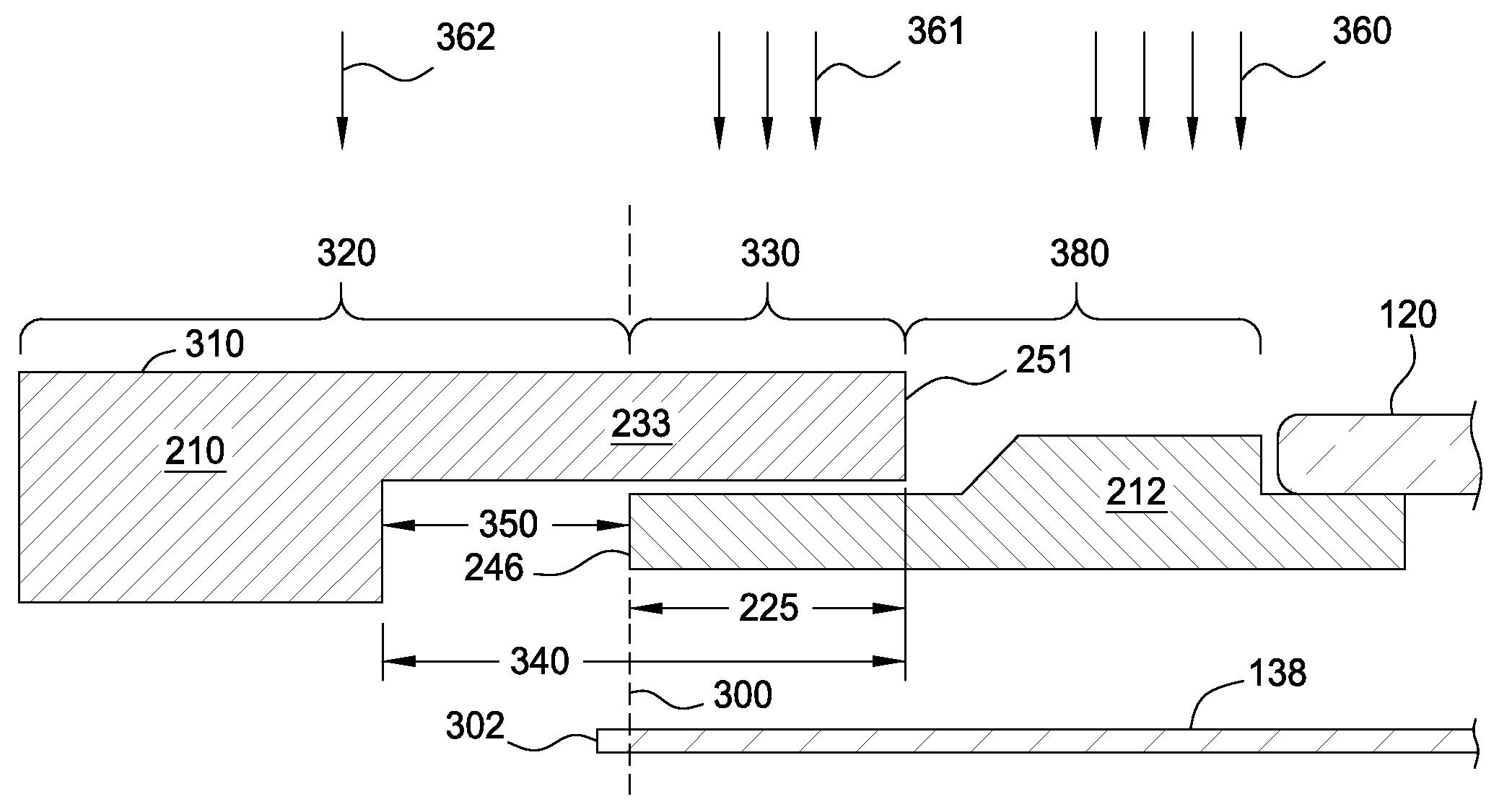
[0052] 외측 석영 링(210)의 외측 부분(234)은 먼쪽 측(far side)(253), 바닥(254) 및 가까운 측(255)을 갖는다. 먼쪽 측(253)은 조정가능한 링 조립체(130)의 최외측 직경(most outer diameter)을 정의한다. 가까운 측(255)은 중간 석영 링(211)과 경계를 접한다(abut). 바닥(254)은 오버랩 부분(233)의 바닥 표면(256)에 평행하고, 그 아래에서 연장하며, 그에 따라 외측 석영 링(210)이 위치적으로(positionally) 기판 지지 페디스털(135) 상에 놓이도록 허용한다. 외측 석영 링(210)과 내측 실리콘 링(212) 사이의 관계뿐 아니라, 이러한 관계에 의해 야기되는, 에칭에 대한 영향은 도 3에 대하여 논의된다.The
[0053] 도 3은, 캐소드 전극(138) 위에서의, 조정가능한 링 조립체(130)의 외측 석영 링(210)과 내측 실리콘 링(212) 사이의 오버랩을 예시한다. 조정가능한 링 조립체(130)의 외측 석영 링(210)과 내측 실리콘 링(212)의 상대적 위치들은, 프로세싱 챔버(100) 내의 플라즈마에 노출되는, 외측 석영 링(210)의 오버랩되지-않은 부분(320)과 오버랩 부분(330), 그리고 프로세싱 챔버(100) 내의 플라즈마에 또한 노출되는, 내측 실리콘 링(212)의 노출된 부분(380)을 정의한다. 내측 실리콘 링(212)의 다른 부분들은 외측 석영 링(210)의 오버랩 부분(330)에 의해 또는 기판(120)에 의해 커버된다(즉, 플라즈마로부터 쉴딩된다). 외측 석영 링(210)의 오버랩 부분(233)은 조정가능한 링 조립체(130)의 반경을 따라 측정된 길이(340)를 갖는다. 외측 석영 링(210)과 내측 실리콘 링(212) 사이에 갭(350)이 도시되어 있다. 갭(350)은, 도 2에 도시된 바와 같이, 중간 석영 링(211)이 링들(210, 212) 사이에 인터피팅되는(interfit) 것을 허용한다.3 illustrates the overlap between the
[0054] 도 3에 도시된 바와 같이, 캐소드 전극(138)은 내측 실리콘 링(212) 아래에서 외경 엣지(302)까지 연장하며, 외경 엣지(302)는 가상선(300)에 의해 예시된 바와 같이, 외측 석영 링(210)의 내측 표면(251) 및 내측 실리콘 링(212)의 먼쪽 표면(246)의 방사상 외측에 있다. 내측 실리콘 링(212) 아래에서의 캐소드 전극(138)의 연장은 기판(120)의 엣지에서의 플라즈마 균일성을 개선한다. 내측 실리콘 링(212)은, (플라즈마에 대해) 기판의 엣지를 그 실제 위치의 외측에 있는 것으로 보이게 하는 실리콘 표면을 제공할 수 있다.As shown in FIG. 3, the
[0055] 외측 석영 링(210) 아래에서의 캐소드 전극(138)의 연장은 오버랩되지-않은 부분(320)에 비해 외측 석영 링(210)의 오버랩 부분(330)을 우선적으로 에칭하며, 그에 따라 기판(120)의 엣지에 근접하여, 외측 석영 링(210)을 구성하는 석영 재료로부터 산소를 방출한다. 방출된 산소는, 폴리머 패시베이션의 양 및 마스크 ― 마스크를 통하여, 기판 상에 배치된 아래에 놓인 층들이 에칭됨 ― 의 개구들의 개방 크기가 제어되도록 허용한다. 예를 들면, 더 큰 오버랩 부분(330)을 갖는 것은 방출되는 산소의 양을 증가시킬 것이며, 그에 따라 마스크 ― 마스크를 통하여, 기판 상에 배치된 하부에 놓인 층들이 에칭됨 ― 의 개구들의 개방을 확대하거나 열린 채로 유지할(keep clear) 것이다. 반대로, 더 작은 오버랩 부분(330)을 갖는 것은 방출되는 산소의 양을 감소시킬 것이며, 그에 따라 에칭 동안, 마스크의 개구들의 개방이 좁아지도록 허용할 것이다. 따라서, 오버랩 부분(330)의 크기(즉, 도 2에 도시된 길이 치수(225))를 제어함으로써, 에칭 프로세스가 조정될 수 있다.Extension of the
[0056] 도 3에는 내측 실리콘 링(212) 위의 플라즈마 이온들(360), 외측 석영 링(210)의 오버랩 부분(330) 가까이의 플라즈마 이온들(361), 및 외측 석영 링(210)의 오버랩되지-않은 부분(320) 가까이의 플라즈마 이온들(362)이 예시된다. 플라즈마 이온들(360)에 대한 반응 레이트는 외측 석영 링(210)의 오버랩 부분(330)의 크기를 변화시킴으로써 조절될 수 있다. 반응 레이트는 플라즈마 이온들의 개수가 증가함에 따라 증가한다. 도시된 바와 같이, 플라즈마 이온들(360)을 도시하는 화살표들의 개수에 의해 도시된, 기판에 가장 가까이에서의 반응 레이트는 기판으로부터 더 멀리에서의 반응 레이트보다 더 높다. 플라즈마 이온들(360)의 증가는 기판의 엣지 가까이에서의 반응 레이트의 증가에 대응한다. 도시된 예에서, 플라즈마 이온들(360)은 내측 실리콘 링(212)의 노출된 부분(380)에 충격을 주고 플라즈마 이온들(361)은 오버랩 부분(330)에 충격을 주는 반면, 플라즈마 이온들(362)은 오버랩되지-않은 부분(320)에 충격을 준다. 그러므로 플라즈마 이온들(360, 361, 362)의 양은 조정가능한 링 조립체(130)에 걸쳐서 불균일하며, 이온들의 농도는 링 조립체의 중심으로부터의 거리가 증가함에 따라 감소한다.3,
[0057] 일 실시예에서, 기판 엣지에서의 플라즈마 반응 레이트는 내측 실리콘 링(212) 위의 외측 석영 링(210)에 대한 오버랩 부분(330)의 크기를 감소시킴으로써 조정될 수 있다. 이는 플라즈마 이온들(360)의 개수를 감소시키는 효과를 갖는다.In one embodiment, the rate of plasma reaction at the substrate edge can be adjusted by reducing the size of the
[0058] 다른 실시예에서, 기판 위에서의 플라즈마 반응 레이트는 불균일하다. 기판의 엣지에서 반응하는 플라즈마 이온들의 개수는 기판의 중앙과 동일한 레이트로 기판을 에칭하기에 충분하지 않다. 외측 석영 링(210)의 오버랩 부분(330)은 더 많은 내측 실리콘 링(212)을 커버하도록 증가될 수 있다. 길이(340)는 오버랩 치수(225)를 대응하게 증가시키도록 증가되며, 플라즈마 이온들(360)의 개수는 그에 따라 또한 증가된다. 대안적으로, 에칭 레이트는, 하나의 구역에 고 종횡비 피쳐들을 갖는 기판이 더 빠르게 에칭될 수 있도록 하는 특정 방식으로 불균일하도록 조정될 수 있다. 그러한 하나의 예는 3D 패키징에서 발견될 수 있는 스텝들(steps)이다.[0058] In another embodiment, the rate of plasma reaction over the substrate is non-uniform. The number of plasma ions reacting at the edge of the substrate is not sufficient to etch the substrate at the same rate as the center of the substrate. The
[0059] 알 수 있는 바와 같이, 기판 엣지에서의 반응 레이트는 외측 석영 링(210)의 오버랩 부분(330)의 치수(225)를 조절함으로써 조정될 수 있다. 일 실시예에서, 기판 엣지를 따라서 반응 레이트가 매우 낮은 경우, 오버랩 부분(330)은 링들(210, 212) 중 하나를 변화시킴으로써 증가될 수 있다.As can be seen, the rate of reaction at the edge of the substrate can be adjusted by adjusting the
[0060] 플라즈마 이온들에 대한 챔버 컴포넌트들의 노출은 유효 수명 및 유지보수 간격들에 크게 영향을 미치기 때문에, 링 조립체(130)에 영향을 주는 이온들의 양을 제어하는 능력은 유리하게 유효 수명을 연장시킨다. 링 조립체(130)는 ESC를 보호할 뿐 아니라, 기판의 표면에 걸쳐서 플라즈마 이온들의 균일성을 제어하는 것을 도움으로써, 플라즈마 프로세스를 향상시킨다.[0060] Since exposure of chamber components to plasma ions greatly affects the useful life and maintenance intervals, the ability to control the amount of ions that affect
[0061] 다양한 실시예들 사이의 차이점들을 보다 잘 예시하기 위해, 도 4는 다양한 링 조립체 구성들에 대한 에칭 레이트를 도시하는 그래프(400)를 제공한다. 그래프(400)는 3개의 실시예들을 도시한다. 제 1 실시예에서, 오버랩핑 부분들이 없는(즉, 길이(255)가 대략 0임) 링 조립체(130)가 트레이스(460)에 의해 도시된다. 제 2 실시예에서, 외측 부분(232)의 약 50 퍼센트가 외측 석영 링(210)과 오버랩핑된 링 조립체(130)가 트레이스(450)에 의해 도시된다. 제 3 실시예에서, 외측 부분(232)의 약 100 퍼센트가 외측 석영 링(210)과 오버랩핑된 링 조립체(130)가 트레이스(440)에 의해 도시된다. 트레이스들(440, 450, 460)은, 에칭 레이트(옹스트롬/분)를 도시하는 축(415) 및 기판(120) 상의 방사상 위치를 예시하는 축(410)을 이용하여 그래프로 도시되며, 기판(120)의 중심을 나타내는 참조 번호(405) 및 엣지를 나타내는 참조 번호(406)를 갖는다.To better illustrate the differences between the various embodiments, FIG. 4 provides a
[0062] 트레이스(460)에 의해 예시된 제 1 실시예에서, 링 조립체의 노출된 부분은 기판 엣지 가까이에서 주로 실리콘으로 구성되며, 기판 엣지에서의 에칭 레이트는 실리콘에 의해 가장 많이 영향을 받는다. 트레이스(460)에 대한 외측 반경(410)에서 볼 수 있는 바와 같이, 에칭 레이트는 엣지(406) 부근에서 떨어진다.In the first embodiment illustrated by the
[0063] 트레이스(450)에 의해 예시된 제 2 실시예에서, 링 조립체는 실리콘 및 석영으로 구성되며, 실리콘 부분이 기판 엣지에 가장 가깝다. 에칭 레이트는 이제, 기판의 엣지에 근접하여 플라즈마에 노출되는 석영의 양에 의해 부분적으로 영향을 받는다. 트레이스(450)에 대한 외측 반경(410)에서 볼 수 있는 바와 같이, 엣지(406)에서의 에칭 레이트는 기판(120)의 중심(405)에서의 에칭 레이트와 거의 동일하다.[0063] In the second embodiment illustrated by
[0064] 트레이스(440)에 의해 예시된 제 3 실시예에서, 링 조립체는 바로 기판 엣지에 대해 석영으로 구성된다. 에칭 레이트는, 기판의 엣지에 근접하여 플라즈마에 노출되는 석영의 양에 의해 상당히 영향을 받는다. 트레이스(440)에 대한 외측 반경(410)에서 볼 수 있는 바와 같이, 엣지(406)에서의 에칭 레이트는 기판(120)의 중심(405)에 대한 에칭 레이트에 비해 상당히 증가한다.[0064] In the third embodiment illustrated by
[0065] 전술한 내용은 본 발명의 실시예들에 관한 것이지만, 본 발명의 기본 범위로부터 벗어나지 않고 본 발명의 다른 그리고 추가의 실시예들이 안출될 수 있으며, 본 발명의 범위는 하기의 청구항들에 의해 결정된다.[0065] The above description relates to embodiments of the present invention, but other and additional embodiments of the present invention may be devised without departing from the basic scope of the present invention, and the scope of the present invention is in the following claims. Determined by
Claims (19)
바닥 표면 및 노출된 최상부 표면을 갖는 외측 세라믹 링; 및
상기 외측 세라믹 링과 정합하여(mate) 오버랩 영역을 정의하도록 구성되는 내측 실리콘 링을 포함하며, 상기 오버랩 영역에서 상기 내측 실리콘 링 위에 놓인 상기 외측 세라믹 링의 구역은 조정가능하고, 상기 외측 세라믹 링의 내부 직경은 상기 구역을 결정하도록 선택가능하고, 상기 내측 실리콘 링은,
내측 표면;
상기 내측 표면에 연결된 바닥 표면;
상기 바닥 표면에 평행한 실질적으로 평평한 최상부 표면;
상기 내측 표면과 상기 최상부 표면 사이에 형성된 노치로서, 상기 내측 표면은 상기 링 조립체의 내경을 정의하고, 상기 노치는,
상기 내측 표면으로부터 연장하는 내측 최상부 표면; 및
상기 내측 최상부 표면으로부터 상기 평평한 최상부 표면까지 연장하는 중간면 ― 상기 노치는 기판의 엣지(edge)를 수용하는 크기로 만들어지며, 상기 오버랩 영역에서 상기 외측 세라믹 링의 높이는 상기 중간면의 길이보다 더 큼 ―;을 포함하는, 상기 노치;
상기 내측 실리콘 링의 외측 부분의 외측 최상부 표면 ― 상기 외측 최상부 표면은 상기 오버랩 영역에서 상기 외측 세라믹 링의 상기 바닥 표면의 내측 부분과 접촉하도록 구성되고 상기 외측 세라믹 링의 상기 바닥 표면의 내측 부분 아래에 놓임 ―; 및
상기 외측 최상부 표면과 상기 평평한 최상부 표면을 연결하면서 방사상 내측으로 그리고 상부로 각진(angled) 경사 표면(inclined surface);을 포함하는,
링 조립체.As a ring assembly:
An outer ceramic ring having a bottom surface and an exposed top surface; And
An inner silicon ring configured to mate with the outer ceramic ring to define an overlap region, wherein a region of the outer ceramic ring overlying the inner silicon ring in the overlap region is adjustable, and The inner diameter is selectable to determine the zone, and the inner silicone ring,
Inner surface;
A floor surface connected to the inner surface;
A substantially flat top surface parallel to the bottom surface;
A notch formed between the inner surface and the top surface, the inner surface defining an inner diameter of the ring assembly, and the notch,
An inner top surface extending from the inner surface; And
An intermediate surface extending from the inner uppermost surface to the flat uppermost surface-The notch is sized to accommodate the edge of the substrate, and the height of the outer ceramic ring in the overlap area is greater than the length of the intermediate surface. -; including, the notch;
An outer top surface of the outer portion of the inner silicon ring, the outer top surface being configured to contact an inner portion of the bottom surface of the outer ceramic ring in the overlap region and below the inner portion of the bottom surface of the outer ceramic ring Placed -; And
Including; a radially inwardly and upwardly angled inclined surface (inclined surface) connecting the outer top surface and the flat top surface,
Ring assembly.
상기 외측 세라믹 링의 상기 바닥 표면의 상기 내측 부분 아래에 놓이는, 상기 내측 실리콘 링의 상기 오버랩 영역 아래에 놓이는 중간 세라믹 링을 더 포함하는
링 조립체.The method of claim 1,
Further comprising an intermediate ceramic ring lying below the overlap region of the inner silicon ring, lying below the inner portion of the bottom surface of the outer ceramic ring
Ring assembly.
상기 경사 표면은 상기 내측 실리콘 링의 상기 평평한 최상부 표면에 대해 45도로 배향되는
링 조립체.The method of claim 1,
The inclined surface is oriented 45 degrees relative to the flat top surface of the inner silicon ring.
Ring assembly.
챔버 본체;
상기 챔버 본체 내에 배치되며, 캐소드 전극이 내부에 배치되는 기판 지지 페디스털; 및
상기 기판 지지 페디스털 상에 배치된 링 조립체를 포함하며, 상기 링 조립체는:
바닥 표면 및 노출된 최상부 표면을 갖는 외측 세라믹 링; 및
상기 외측 세라믹 링과 정합하여(mate) 오버랩 영역을 정의하도록 구성되는 내측 실리콘 링을 포함하며, 상기 오버랩 영역에서 상기 내측 실리콘 링 위에 놓인 상기 외측 세라믹 링의 구역은 조정가능하고, 상기 외측 세라믹 링의 내부 직경은 상기 구역을 결정하도록 선택가능하고, 상기 내측 실리콘 링은,
내측 표면;
실질적으로 평평한 최상부 표면;
상기 내측 표면과 상기 평평한 최상부 표면 사이에 형성된 노치로서, 상기 내측 표면은 상기 링 조립체의 내경을 정의하고, 상기 노치는,
상기 내측 표면으로부터 연장하는 내측 최상부 표면; 및
상기 내측 최상부 표면으로부터 상기 최상부 표면까지 연장하는 중간면 ― 상기 노치는 기판의 엣지(edge)를 수용하는 크기로 만들어지며, 상기 오버랩 영역에서 상기 외측 세라믹 링의 높이는 상기 중간면의 길이보다 더 큼 ―;을 포함하는, 상기 노치;
상기 내측 실리콘 링의 외측 최상부 표면 ― 상기 외측 최상부 표면은 오버랩 영역에서 상기 외측 세라믹 링의 상기 바닥 표면의 내측 부분과 접촉하도록 구성되고 상기 외측 세라믹 링의 상기 바닥 표면의 내측 부분 아래에 놓이고, 상기 오버랩 영역은 상기 캐소드 전극 위에 배치됨 ―; 및
상기 외측 최상부 표면과 상기 최상부 표면을 연결하면서 방사상 내측으로 그리고 상부로 각진(angled) 경사 표면(inclined surface);을 포함하는,
플라즈마 프로세싱 챔버.As a plasma processing chamber:
Chamber body;
A substrate supporting pedestal disposed in the chamber body and having a cathode electrode disposed therein; And
A ring assembly disposed on the substrate support pedestal, the ring assembly comprising:
An outer ceramic ring having a bottom surface and an exposed top surface; And
An inner silicon ring configured to mate with the outer ceramic ring to define an overlap region, wherein a region of the outer ceramic ring overlying the inner silicon ring in the overlap region is adjustable, and The inner diameter is selectable to determine the zone, and the inner silicone ring,
Inner surface;
A substantially flat top surface;
A notch formed between the inner surface and the flat top surface, the inner surface defining an inner diameter of the ring assembly, and the notch,
An inner top surface extending from the inner surface; And
An intermediate surface extending from the inner uppermost surface to the uppermost surface-the notch is made in a size to accommodate an edge of the substrate, and the height of the outer ceramic ring in the overlap area is greater than the length of the intermediate surface- Including; the notch;
An outer top surface of the inner silicon ring, the outer top surface being configured to contact an inner portion of the bottom surface of the outer ceramic ring in an overlap region and lying below an inner portion of the bottom surface of the outer ceramic ring, the An overlap region is disposed over the cathode electrode; And
Including; a radially inwardly and upwardly angled inclined surface (inclined surface) connecting the outer uppermost surface and the uppermost surface;
Plasma processing chamber.
상기 캐소드 전극은 상기 내측 실리콘 링을 지나서(beyond) 연장하는
플라즈마 프로세싱 챔버.The method of claim 5,
The cathode electrode extends beyond the inner silicon ring
Plasma processing chamber.
상기 외측 세라믹 링의 상기 바닥 표면의 내측 부분 아래에 놓이는, 상기 내측 실리콘 링의 상기 오버랩 영역 아래에 놓이는 중간 세라믹 링을 더 포함하는
플라즈마 프로세싱 챔버.The method of claim 5,
Further comprising an intermediate ceramic ring lying below the overlap region of the inner silicon ring, lying below an inner portion of the bottom surface of the outer ceramic ring
Plasma processing chamber.
상기 오버랩 영역은 0보다 크고 30 mm 이하의 방사상 치수를 갖는
플라즈마 프로세싱 챔버.The method of claim 5,
The overlap area is greater than 0 and has a radial dimension of 30 mm or less.
Plasma processing chamber.
상기 외측 세라믹 링은 상기 내측 실리콘 링을 따라, 상기 노치로부터 30 mm까지 연장하는
플라즈마 프로세싱 챔버.The method of claim 5,
The outer ceramic ring extends from the notch to 30 mm along the inner silicon ring
Plasma processing chamber.
상기 경사 표면은 상기 내측 실리콘 링의 상기 최상부 표면에 대해 45도로 배향되는
플라즈마 프로세싱 챔버.The method of claim 5,
The inclined surface is oriented 45 degrees with respect to the top surface of the inner silicon ring.
Plasma processing chamber.
상기 링 조립체에 의해 외접하여 둘러싸이는(circumscribed) 제 1 기판을 에칭하는 단계 ― 상기 링 조립체는 오버랩 영역을 정의하도록 정합하는 실리콘 내측 링 및 세라믹 외측 링을 가짐 ―;
상기 오버랩 영역을 변화시키기 위해 상기 실리콘 내측 링과 상기 세라믹 외측 링 중 적어도 하나를 대체하는 단계; 및
변화된 상기 오버랩 영역을 갖는 상기 링 조립체의 존재하에서 제 2 기판을 에칭하는 단계를 포함하는
링 조립체를 이용하여 에칭 레이트를 조정하기 위한 방법.As a method for adjusting the etch rate using a ring assembly:
Etching a first substrate circumscribed by the ring assembly, the ring assembly having a silicon inner ring and a ceramic outer ring mating to define an overlap area;
Replacing at least one of the silicon inner ring and the ceramic outer ring to change the overlap area; And
Etching a second substrate in the presence of the ring assembly having the altered overlap region.
A method for adjusting the etch rate using a ring assembly.
상기 대체하는 단계는 상기 오버랩 영역의 치수를 증가시키는 것을 포함하는
링 조립체를 이용하여 에칭 레이트를 조정하기 위한 방법.The method of claim 12,
The replacing step comprises increasing the dimension of the overlap area.
A method for adjusting the etch rate using a ring assembly.
상기 대체하는 단계는 상기 오버랩 영역의 치수를 감소시키는 것을 포함하는
링 조립체를 이용하여 에칭 레이트를 조정하기 위한 방법.The method of claim 12,
The replacing step comprises reducing the dimension of the overlap area.
A method for adjusting the etch rate using a ring assembly.
상기 제 1 기판을 에칭하는 단계는:
상기 세라믹 외측 링으로부터의 산소를 드라이빙하도록(drive) 캐소드 전극을 에너자이징하는 단계를 포함하는
링 조립체를 이용하여 에칭 레이트를 조정하기 위한 방법.The method of claim 12,
Etching the first substrate comprises:
Energizing a cathode electrode to drive oxygen from the ceramic outer ring.
A method for adjusting the etch rate using a ring assembly.
상기 외측 세라믹 링은, 먼쪽 측, 바닥 측, 및 가까운 측을 갖는 외측 부분을 갖고, 상기 오버랩 영역은, 상기 외측 세라믹 링과 내측 석영 링 사이에 중간 세라믹 링을 인터피팅하도록(interfit) 구성되는 갭을 정의하는,
링 조립체.The method of claim 2,
The outer ceramic ring has an outer portion having a far side, a bottom side, and a near side, and the overlap region is a gap configured to interfit an intermediate ceramic ring between the outer ceramic ring and the inner quartz ring. To define,
Ring assembly.
상기 실질적으로 평평한 최상부 표면은 상기 외측 최상부 표면과 평행한,
링 조립체.The method of claim 1,
The substantially flat top surface is parallel to the outer top surface,
Ring assembly.
상기 내측 최상부 표면은 상기 외측 최상부 표면과 동일평면인,
링 조립체.The method of claim 1,
The inner top surface is flush with the outer top surface,
Ring assembly.
상기 외측 세라믹 링의 상기 노출된 최상부 표면은, 상기 내측 실리콘 링의 상기 평평한 최상부 표면에 수직으로 위에 있는,
링 조립체.
The method of claim 1,
The exposed top surface of the outer ceramic ring is perpendicular to the flat top surface of the inner silicon ring,
Ring assembly.
Applications Claiming Priority (5)
| Application Number | Priority Date | Filing Date | Title |
|---|---|---|---|
| US201361841194P | 2013-06-28 | 2013-06-28 | |
| US61/841,194 | 2013-06-28 | ||
| US14/020,774 | 2013-09-06 | ||
| US14/020,774 US20150001180A1 (en) | 2013-06-28 | 2013-09-06 | Process kit for edge critical dimension uniformity control |
| PCT/US2014/036010 WO2014209489A1 (en) | 2013-06-28 | 2014-04-30 | Process kit for edge critical dimension uniformity control |
Publications (2)
| Publication Number | Publication Date |
|---|---|
| KR20160029073A KR20160029073A (en) | 2016-03-14 |
| KR102190302B1 true KR102190302B1 (en) | 2020-12-11 |
Family
ID=52114576
Family Applications (1)
| Application Number | Title | Priority Date | Filing Date |
|---|---|---|---|
| KR1020167000788A Active KR102190302B1 (en) | 2013-06-28 | 2014-04-30 | Process kit for edge critical dimension uniformity control |
Country Status (6)
| Country | Link |
|---|---|
| US (1) | US20150001180A1 (en) |
| JP (2) | JP6867159B2 (en) |
| KR (1) | KR102190302B1 (en) |
| CN (1) | CN105283944B (en) |
| TW (1) | TWM495617U (en) |
| WO (1) | WO2014209489A1 (en) |
Families Citing this family (19)
| Publication number | Priority date | Publication date | Assignee | Title |
|---|---|---|---|---|
| US10358721B2 (en) * | 2015-10-22 | 2019-07-23 | Asm Ip Holding B.V. | Semiconductor manufacturing system including deposition apparatus |
| US9691625B2 (en) * | 2015-11-04 | 2017-06-27 | Lam Research Corporation | Methods and systems for plasma etching using bi-modal process gas composition responsive to plasma power level |
| JP7098273B2 (en) | 2016-03-04 | 2022-07-11 | アプライド マテリアルズ インコーポレイテッド | Universal process kit |
| US9947517B1 (en) * | 2016-12-16 | 2018-04-17 | Applied Materials, Inc. | Adjustable extended electrode for edge uniformity control |
| US12293902B2 (en) | 2018-01-19 | 2025-05-06 | Applied Materials, Inc. | Process kit for a substrate support |
| US11387134B2 (en) * | 2018-01-19 | 2022-07-12 | Applied Materials, Inc. | Process kit for a substrate support |
| US20190287835A1 (en) * | 2018-02-01 | 2019-09-19 | Yield Engineering Systems, Inc. | Interchangeable Edge Rings For Stabilizing Wafer Placement And System Using Same |
| SG11202010375QA (en) | 2018-04-20 | 2020-11-27 | Lam Res Corp | Edge exclusion control |
| JP7138514B2 (en) * | 2018-08-22 | 2022-09-16 | 東京エレクトロン株式会社 | Annular member, plasma processing apparatus and plasma etching method |
| JP7541005B2 (en) * | 2018-12-03 | 2024-08-27 | アプライド マテリアルズ インコーポレイテッド | Electrostatic chuck design with improved chuck and arcing performance |
| US12476082B2 (en) * | 2020-02-04 | 2025-11-18 | Lam Research Corporation | Radiofrequency signal filter arrangement for plasma processing system |
| KR20220010074A (en) | 2020-02-11 | 2022-01-25 | 램 리써치 코포레이션 | Carrier Ring Designs to Control Deposition on Wafer Bevel/Edge |
| CN111508803B (en) * | 2020-04-23 | 2023-01-17 | 北京北方华创微电子装备有限公司 | Semiconductor process chamber, wafer edge protection method and semiconductor equipment |
| CN113802111B (en) * | 2020-06-13 | 2023-10-31 | 拓荆科技股份有限公司 | Equipment for treating substrates using plasma and methods for improving surface morphology of wafer thin films |
| US20230238223A1 (en) * | 2020-06-25 | 2023-07-27 | Lam Research Corporation | Carrier rings with radially-varied plasma impedance |
| FI130020B (en) * | 2021-05-10 | 2022-12-30 | Picosun Oy | Substrate processing apparatus and method |
| US20230066418A1 (en) * | 2021-08-30 | 2023-03-02 | Taiwan Semiconductor Manufacturing Company, Ltd. | Focus ring for a plasma-based semiconductor processing tool |
| KR102744850B1 (en) * | 2022-08-10 | 2024-12-19 | 솔믹스 주식회사 | Focus ring and apparatus of plasma etching comprising the same |
| CN115910738B (en) * | 2022-11-01 | 2025-02-18 | 上海积塔半导体有限公司 | A method to adjust the uniformity of the Emax process chamber by changing the component size |
Citations (1)
| Publication number | Priority date | Publication date | Assignee | Title |
|---|---|---|---|---|
| JP2011035026A (en) * | 2009-07-30 | 2011-02-17 | Seiko Epson Corp | Dry etching device, method of manufacturing semiconductor device, and control ring |
Family Cites Families (24)
| Publication number | Priority date | Publication date | Assignee | Title |
|---|---|---|---|---|
| JP3121524B2 (en) * | 1995-06-07 | 2001-01-09 | 東京エレクトロン株式会社 | Etching equipment |
| US6284093B1 (en) * | 1996-11-29 | 2001-09-04 | Applied Materials, Inc. | Shield or ring surrounding semiconductor workpiece in plasma chamber |
| WO1999014788A1 (en) * | 1997-09-16 | 1999-03-25 | Applied Materials, Inc. | Shield or ring surrounding semiconductor workpiece in plasma chamber |
| JP3296300B2 (en) * | 1998-08-07 | 2002-06-24 | ウシオ電機株式会社 | Light irradiation type heating device |
| KR20010089376A (en) * | 1998-10-29 | 2001-10-06 | 조셉 제이. 스위니 | Apparatus for coupling power through a workpiece in a semiconductor wafer processing system |
| JP3764639B2 (en) * | 2000-09-13 | 2006-04-12 | 株式会社日立製作所 | Plasma processing apparatus and semiconductor device manufacturing method |
| JP4676074B2 (en) * | 2001-02-15 | 2011-04-27 | 東京エレクトロン株式会社 | Focus ring and plasma processing apparatus |
| JP4209618B2 (en) * | 2002-02-05 | 2009-01-14 | 東京エレクトロン株式会社 | Plasma processing apparatus and ring member |
| JP2003257935A (en) * | 2002-03-05 | 2003-09-12 | Tokyo Electron Ltd | Plasma treatment apparatus |
| AU2002366921A1 (en) * | 2001-12-13 | 2003-07-09 | Tokyo Electron Limited | Ring mechanism, and plasma processing device using the ring mechanism |
| US6868302B2 (en) * | 2002-03-25 | 2005-03-15 | Dainippon Screen Mfg. Co., Ltd. | Thermal processing apparatus |
| JP4286025B2 (en) * | 2003-03-03 | 2009-06-24 | 川崎マイクロエレクトロニクス株式会社 | Method of reclaiming quartz jig, method of reusing and using semiconductor device |
| JP2005167088A (en) * | 2003-12-04 | 2005-06-23 | Matsushita Electric Ind Co Ltd | Dry etching apparatus and dry etching method |
| US7244336B2 (en) * | 2003-12-17 | 2007-07-17 | Lam Research Corporation | Temperature controlled hot edge ring assembly for reducing plasma reactor etch rate drift |
| JP2005303099A (en) * | 2004-04-14 | 2005-10-27 | Hitachi High-Technologies Corp | Plasma processing apparatus and plasma processing method |
| JP2006086230A (en) * | 2004-09-14 | 2006-03-30 | Hitachi Kokusai Electric Inc | Semiconductor manufacturing equipment |
| US7520969B2 (en) * | 2006-03-07 | 2009-04-21 | Applied Materials, Inc. | Notched deposition ring |
| KR100794308B1 (en) * | 2006-05-03 | 2008-01-11 | 삼성전자주식회사 | Semiconductor plasma device |
| US8440049B2 (en) * | 2006-05-03 | 2013-05-14 | Applied Materials, Inc. | Apparatus for etching high aspect ratio features |
| US20070283884A1 (en) * | 2006-05-30 | 2007-12-13 | Applied Materials, Inc. | Ring assembly for substrate processing chamber |
| JP5035884B2 (en) * | 2007-03-27 | 2012-09-26 | 東京エレクトロン株式会社 | Thermal conductive sheet and substrate mounting apparatus using the same |
| US8622021B2 (en) * | 2007-10-31 | 2014-01-07 | Lam Research Corporation | High lifetime consumable silicon nitride-silicon dioxide plasma processing components |
| JP2010045200A (en) * | 2008-08-13 | 2010-02-25 | Tokyo Electron Ltd | Focus ring, and plasma processing apparatus and method |
| JP5719599B2 (en) * | 2011-01-07 | 2015-05-20 | 東京エレクトロン株式会社 | Substrate processing equipment |
-
2013
- 2013-09-06 US US14/020,774 patent/US20150001180A1/en not_active Abandoned
-
2014
- 2014-04-30 WO PCT/US2014/036010 patent/WO2014209489A1/en not_active Ceased
- 2014-04-30 JP JP2016523735A patent/JP6867159B2/en active Active
- 2014-04-30 KR KR1020167000788A patent/KR102190302B1/en active Active
- 2014-04-30 CN CN201480033790.1A patent/CN105283944B/en active Active
- 2014-05-02 TW TW103207716U patent/TWM495617U/en not_active IP Right Cessation
-
2020
- 2020-09-30 JP JP2020164401A patent/JP2021010016A/en active Pending
Patent Citations (1)
| Publication number | Priority date | Publication date | Assignee | Title |
|---|---|---|---|---|
| JP2011035026A (en) * | 2009-07-30 | 2011-02-17 | Seiko Epson Corp | Dry etching device, method of manufacturing semiconductor device, and control ring |
Also Published As
| Publication number | Publication date |
|---|---|
| US20150001180A1 (en) | 2015-01-01 |
| JP2016530705A (en) | 2016-09-29 |
| TWM495617U (en) | 2015-02-11 |
| WO2014209489A1 (en) | 2014-12-31 |
| KR20160029073A (en) | 2016-03-14 |
| JP6867159B2 (en) | 2021-04-28 |
| CN105283944B (en) | 2018-04-27 |
| JP2021010016A (en) | 2021-01-28 |
| CN105283944A (en) | 2016-01-27 |
Similar Documents
| Publication | Publication Date | Title |
|---|---|---|
| KR102190302B1 (en) | Process kit for edge critical dimension uniformity control | |
| JP6853038B2 (en) | Single ring design for high yield and reduction of substrate edge defects in ICP plasma processing chamber | |
| TWI433215B (en) | Substrate cleaning chamber and method for cleaning and adjusting | |
| CN205984889U (en) | A edge ring for inclined plane polymer reduces | |
| CN113039626B (en) | Edge Ring Temperature and Bias Control | |
| EP2819151B1 (en) | Plasma etching method and plasma etching apparatus | |
| US20140017900A1 (en) | Plasma etching apparatus and plasma etching method | |
| KR20190068490A (en) | Bottom ring and middle edge ring | |
| US9263239B1 (en) | Etching method of multilayered film | |
| JP5808750B2 (en) | Electrostatic chuck with inclined side walls | |
| KR20160117261A (en) | Plasma processing systems and structures having sloped confinement rings | |
| KR102505154B1 (en) | etching method | |
| US10553442B2 (en) | Etching method | |
| JP7801323B2 (en) | Chamber configuration and process for particle control | |
| JP7427108B2 (en) | Low resistance confinement liner for use in plasma chambers | |
| TW202146694A (en) | Exclusion ring with flow paths for exhausting wafer edge gas | |
| JP2026000968A (en) | Processing Chamber Deposition Confinement | |
| TWI889733B (en) | Substrate processing method and substrate processing apparatus | |
| TWI874452B (en) | Substrate processing method, method for manufacturing semiconducor device, and plasma processing apparatus | |
| US20220356584A1 (en) | Substrate processing method and substrate processing apparatus | |
| TWI798856B (en) | Semiconductor processing system and method for bevel backside deposition elimination |
Legal Events
| Date | Code | Title | Description |
|---|---|---|---|
| PA0105 | International application |
St.27 status event code: A-0-1-A10-A15-nap-PA0105 |
|
| P11-X000 | Amendment of application requested |
St.27 status event code: A-2-2-P10-P11-nap-X000 |
|
| P13-X000 | Application amended |
St.27 status event code: A-2-2-P10-P13-nap-X000 |
|
| P11-X000 | Amendment of application requested |
St.27 status event code: A-2-2-P10-P11-nap-X000 |
|
| P13-X000 | Application amended |
St.27 status event code: A-2-2-P10-P13-nap-X000 |
|
| R15-X000 | Change to inventor requested |
St.27 status event code: A-3-3-R10-R15-oth-X000 |
|
| R16-X000 | Change to inventor recorded |
St.27 status event code: A-3-3-R10-R16-oth-X000 |
|
| PG1501 | Laying open of application |
St.27 status event code: A-1-1-Q10-Q12-nap-PG1501 |
|
| A201 | Request for examination | ||
| E13-X000 | Pre-grant limitation requested |
St.27 status event code: A-2-3-E10-E13-lim-X000 |
|
| P11-X000 | Amendment of application requested |
St.27 status event code: A-2-2-P10-P11-nap-X000 |
|
| P13-X000 | Application amended |
St.27 status event code: A-2-2-P10-P13-nap-X000 |
|
| PA0201 | Request for examination |
St.27 status event code: A-1-2-D10-D11-exm-PA0201 |
|
| D13-X000 | Search requested |
St.27 status event code: A-1-2-D10-D13-srh-X000 |
|
| D14-X000 | Search report completed |
St.27 status event code: A-1-2-D10-D14-srh-X000 |
|
| E902 | Notification of reason for refusal | ||
| PE0902 | Notice of grounds for rejection |
St.27 status event code: A-1-2-D10-D21-exm-PE0902 |
|
| P11-X000 | Amendment of application requested |
St.27 status event code: A-2-2-P10-P11-nap-X000 |
|
| P13-X000 | Application amended |
St.27 status event code: A-2-2-P10-P13-nap-X000 |
|
| E701 | Decision to grant or registration of patent right | ||
| PE0701 | Decision of registration |
St.27 status event code: A-1-2-D10-D22-exm-PE0701 |
|
| GRNT | Written decision to grant | ||
| PR0701 | Registration of establishment |
St.27 status event code: A-2-4-F10-F11-exm-PR0701 |
|
| PR1002 | Payment of registration fee |
St.27 status event code: A-2-2-U10-U12-oth-PR1002 Fee payment year number: 1 |
|
| PG1601 | Publication of registration |
St.27 status event code: A-4-4-Q10-Q13-nap-PG1601 |
|
| PR1001 | Payment of annual fee |
St.27 status event code: A-4-4-U10-U11-oth-PR1001 Fee payment year number: 4 |
|
| PR1001 | Payment of annual fee |
St.27 status event code: A-4-4-U10-U11-oth-PR1001 Fee payment year number: 5 |
|
| PR1001 | Payment of annual fee |
St.27 status event code: A-4-4-U10-U11-oth-PR1001 Fee payment year number: 6 |
|
| U11 | Full renewal or maintenance fee paid |
Free format text: ST27 STATUS EVENT CODE: A-4-4-U10-U11-OTH-PR1001 (AS PROVIDED BY THE NATIONAL OFFICE) Year of fee payment: 6 |
|
| P22-X000 | Classification modified |
St.27 status event code: A-4-4-P10-P22-nap-X000 |