KR102173811B1 - Package unit and multi-stack package - Google Patents
Package unit and multi-stack package Download PDFInfo
- Publication number
- KR102173811B1 KR102173811B1 KR1020190057602A KR20190057602A KR102173811B1 KR 102173811 B1 KR102173811 B1 KR 102173811B1 KR 1020190057602 A KR1020190057602 A KR 1020190057602A KR 20190057602 A KR20190057602 A KR 20190057602A KR 102173811 B1 KR102173811 B1 KR 102173811B1
- Authority
- KR
- South Korea
- Prior art keywords
- semiconductor dies
- encapsulant
- package
- active surface
- encapsulation member
- Prior art date
- Legal status (The legal status is an assumption and is not a legal conclusion. Google has not performed a legal analysis and makes no representation as to the accuracy of the status listed.)
- Active
Links
Images


Classifications
-
- H—ELECTRICITY
- H01—ELECTRIC ELEMENTS
- H01L—SEMICONDUCTOR DEVICES NOT COVERED BY CLASS H10
- H01L25/00—Assemblies consisting of a plurality of semiconductor or other solid state devices
- H01L25/03—Assemblies consisting of a plurality of semiconductor or other solid state devices all the devices being of a type provided for in a single subclass of subclasses H10B, H10D, H10F, H10H, H10K or H10N, e.g. assemblies of rectifier diodes
- H01L25/04—Assemblies consisting of a plurality of semiconductor or other solid state devices all the devices being of a type provided for in a single subclass of subclasses H10B, H10D, H10F, H10H, H10K or H10N, e.g. assemblies of rectifier diodes the devices not having separate containers
- H01L25/065—Assemblies consisting of a plurality of semiconductor or other solid state devices all the devices being of a type provided for in a single subclass of subclasses H10B, H10D, H10F, H10H, H10K or H10N, e.g. assemblies of rectifier diodes the devices not having separate containers the devices being of a type provided for in group H10D89/00
- H01L25/0652—Assemblies consisting of a plurality of semiconductor or other solid state devices all the devices being of a type provided for in a single subclass of subclasses H10B, H10D, H10F, H10H, H10K or H10N, e.g. assemblies of rectifier diodes the devices not having separate containers the devices being of a type provided for in group H10D89/00 the devices being arranged next and on each other, i.e. mixed assemblies
-
- H10W90/00—
-
- H—ELECTRICITY
- H01—ELECTRIC ELEMENTS
- H01L—SEMICONDUCTOR DEVICES NOT COVERED BY CLASS H10
- H01L23/00—Details of semiconductor or other solid state devices
- H01L23/28—Encapsulations, e.g. encapsulating layers, coatings, e.g. for protection
- H01L23/31—Encapsulations, e.g. encapsulating layers, coatings, e.g. for protection characterised by the arrangement or shape
-
- H—ELECTRICITY
- H01—ELECTRIC ELEMENTS
- H01L—SEMICONDUCTOR DEVICES NOT COVERED BY CLASS H10
- H01L23/00—Details of semiconductor or other solid state devices
- H01L23/52—Arrangements for conducting electric current within the device in operation from one component to another, i.e. interconnections, e.g. wires, lead frames
- H01L23/522—Arrangements for conducting electric current within the device in operation from one component to another, i.e. interconnections, e.g. wires, lead frames including external interconnections consisting of a multilayer structure of conductive and insulating layers inseparably formed on the semiconductor body
- H01L23/5226—Via connections in a multilevel interconnection structure
-
- H—ELECTRICITY
- H01—ELECTRIC ELEMENTS
- H01L—SEMICONDUCTOR DEVICES NOT COVERED BY CLASS H10
- H01L23/00—Details of semiconductor or other solid state devices
- H01L23/52—Arrangements for conducting electric current within the device in operation from one component to another, i.e. interconnections, e.g. wires, lead frames
- H01L23/522—Arrangements for conducting electric current within the device in operation from one component to another, i.e. interconnections, e.g. wires, lead frames including external interconnections consisting of a multilayer structure of conductive and insulating layers inseparably formed on the semiconductor body
- H01L23/5227—Inductive arrangements or effects of, or between, wiring layers
-
- H—ELECTRICITY
- H01—ELECTRIC ELEMENTS
- H01L—SEMICONDUCTOR DEVICES NOT COVERED BY CLASS H10
- H01L23/00—Details of semiconductor or other solid state devices
- H01L23/52—Arrangements for conducting electric current within the device in operation from one component to another, i.e. interconnections, e.g. wires, lead frames
- H01L23/522—Arrangements for conducting electric current within the device in operation from one component to another, i.e. interconnections, e.g. wires, lead frames including external interconnections consisting of a multilayer structure of conductive and insulating layers inseparably formed on the semiconductor body
- H01L23/528—Layout of the interconnection structure
-
- H—ELECTRICITY
- H01—ELECTRIC ELEMENTS
- H01L—SEMICONDUCTOR DEVICES NOT COVERED BY CLASS H10
- H01L24/00—Arrangements for connecting or disconnecting semiconductor or solid-state bodies; Methods or apparatus related thereto
- H01L24/01—Means for bonding being attached to, or being formed on, the surface to be connected, e.g. chip-to-package, die-attach, "first-level" interconnects; Manufacturing methods related thereto
- H01L24/26—Layer connectors, e.g. plate connectors, solder or adhesive layers; Manufacturing methods related thereto
- H01L24/28—Structure, shape, material or disposition of the layer connectors prior to the connecting process
- H01L24/30—Structure, shape, material or disposition of the layer connectors prior to the connecting process of a plurality of layer connectors
-
- H—ELECTRICITY
- H01—ELECTRIC ELEMENTS
- H01L—SEMICONDUCTOR DEVICES NOT COVERED BY CLASS H10
- H01L25/00—Assemblies consisting of a plurality of semiconductor or other solid state devices
- H01L25/03—Assemblies consisting of a plurality of semiconductor or other solid state devices all the devices being of a type provided for in a single subclass of subclasses H10B, H10D, H10F, H10H, H10K or H10N, e.g. assemblies of rectifier diodes
- H01L25/04—Assemblies consisting of a plurality of semiconductor or other solid state devices all the devices being of a type provided for in a single subclass of subclasses H10B, H10D, H10F, H10H, H10K or H10N, e.g. assemblies of rectifier diodes the devices not having separate containers
- H01L25/065—Assemblies consisting of a plurality of semiconductor or other solid state devices all the devices being of a type provided for in a single subclass of subclasses H10B, H10D, H10F, H10H, H10K or H10N, e.g. assemblies of rectifier diodes the devices not having separate containers the devices being of a type provided for in group H10D89/00
- H01L25/0657—Stacked arrangements of devices
-
- H10W72/30—
-
- H10W74/10—
-
- H10W70/099—
-
- H10W72/073—
-
- H10W72/874—
-
- H10W72/9413—
-
- H10W90/22—
-
- H10W90/732—
Landscapes
- Engineering & Computer Science (AREA)
- Microelectronics & Electronic Packaging (AREA)
- Power Engineering (AREA)
- Physics & Mathematics (AREA)
- Computer Hardware Design (AREA)
- Condensed Matter Physics & Semiconductors (AREA)
- General Physics & Mathematics (AREA)
- Geometry (AREA)
- Structures Or Materials For Encapsulating Or Coating Semiconductor Devices Or Solid State Devices (AREA)
- Encapsulation Of And Coatings For Semiconductor Or Solid State Devices (AREA)
Abstract
활성면들을 부분적으로 노출하도록 오프셋되어 적층된 복수의 반도체 다이들; 상기 복수의 반도체 다이들의 노출된 상기 활성면을 피복하고, 상기 활성면에 평행한 제 1 면 및 제 2 면을 갖고, 감광성 절연막을 포함하는 제 1 봉지체; 상기 제 1 면으로부터 상기 제 1 봉지체를 관통하여 상기 활성면까지 연장되는 관통 비아들; 및 상기 제 1 봉지체의 제 1 면 위에서 상기 관통 비아들을 연결하는 상부 배선들을 포함하는 패키지 유닛이 제공된다.A plurality of semiconductor dies offset and stacked to partially expose active surfaces; A first encapsulation member covering the exposed active surface of the plurality of semiconductor dies, having first and second surfaces parallel to the active surface, and including a photosensitive insulating film; Through vias extending from the first surface to the active surface through the first encapsulation member; And upper wirings connecting the through vias on a first surface of the first encapsulant is provided.
Description
본 발명은 패키지 유닛 및 멀티 스택 패키지에 관한 것으로서, 보다 구체적으로는 제조가 간단하고 신속하며 비용이 저렴한 패키지 유닛 및 멀티 스택 패키지에 관한 것이다.The present invention relates to a package unit and a multi-stack package, and more particularly, to a package unit and a multi-stack package that are simple, fast, and inexpensive to manufacture.
메모리 저장 용량이 고용량화되는 반면, 반도체 메모리 소자를 포함하는 전자 장치는 얇고 가벼워질 것이 요구되기 때문에 다수의 반도체 칩들을 적층하는 멀티칩 패키지의 제조 방법에 있어서 여전히 개선할 점들이 있다.While memory storage capacity is increased, electronic devices including semiconductor memory devices are required to be thin and light, so there are still points to be improved in a method of manufacturing a multichip package in which a plurality of semiconductor chips are stacked.
본 발명이 이루고자 하는 첫 번째 기술적 과제는 제조가 간단하고 신속하며 비용이 저렴한 패키지 유닛을 제공하는 것이다.The first technical problem to be achieved by the present invention is to provide a package unit that is simple, fast, and inexpensive to manufacture.
본 발명이 이루고자 하는 두 번째 기술적 과제는 제조가 간단하고 신속하며 비용이 저렴한 멀티 스택 패키지를 제공하는 것이다.A second technical problem to be achieved by the present invention is to provide a multi-stack package that is simple, fast and inexpensive to manufacture.
본 발명이 이루고자 하는 세 번째 기술적 과제는 제조가 간단하고 신속하며 비용이 저렴한 패키지 유닛의 제조 방법을 제공하는 것이다.A third technical problem to be achieved by the present invention is to provide a method of manufacturing a package unit that is simple, fast, and inexpensive to manufacture.
본 발명은 상기 첫 번째 기술적 과제를 이루기 위하여 활성면들을 부분적으로 노출하도록 오프셋되어 적층된 복수의 반도체 다이들; 상기 복수의 반도체 다이들의 노출된 상기 활성면을 피복하고, 상기 활성면에 평행한 제 1 면 및 제 2 면을 갖고, 감광성 절연막을 포함하는 제 1 봉지체; 상기 제 1 면으로부터 상기 제 1 봉지체를 관통하여 상기 활성면까지 연장되는 관통 비아들; 및 상기 제 1 봉지체의 제 1 면 위에서 상기 관통 비아들을 연결하는 상부 배선들을 포함하는 패키지 유닛을 제공한다.In order to achieve the first technical problem, the present invention includes: a plurality of semiconductor dies stacked to be offset to partially expose active surfaces; A first encapsulation member covering the exposed active surface of the plurality of semiconductor dies, having first and second surfaces parallel to the active surface, and including a photosensitive insulating film; Through vias extending from the first surface to the active surface through the first encapsulation member; And upper wirings connecting the through vias on a first surface of the first encapsulation member.
일부 실시예들에 있어서, 상기 감광성 절연막은 폴리이미드계 수지일 수 있다. 일부 실시예들에 있어서, 상기 복수의 반도체 다이들 중 최상위에 위치하는 반도체 다이의 상부면 전체를 상기 제 1 봉지체가 피복하도록 구성될 수 있다.In some embodiments, the photosensitive insulating layer may be a polyimide resin. In some embodiments, the first encapsulant may be configured to cover the entire upper surface of the uppermost semiconductor die among the plurality of semiconductor dies.
일부 실시예들에 있어서, 상기 복수의 반도체 다이들은 상기 활성면들의 반대면인 비활성면을 각각 포함하고, 상기 비활성면과 접촉하며 상기 복수의 반도체 다이들을 피복하는 제 2 봉지체를 더 포함하고, 상기 제 2 봉지체는 상기 제 1 봉지체와 상이할 수 있다. 상기 제 2 봉지체는 에폭시 몰딩 컴파운드(epoxy molding compound, EMC)를 포함할 수 있다. 상기 제 2 면은 최하위에 위치하는 반도체 다이의 상기 비활성면과 실질적으로 동일 평면 위에 있을 수 있다. 상기 제 1 봉지체 및 상기 제 2 봉지체 중 적어도 하나의 측면 상에 프레임 잔여부를 더 포함할 수 있다.In some embodiments, the plurality of semiconductor dies each include an inactive surface opposite to the active surfaces, and further include a second encapsulant in contact with the inactive surface and covering the plurality of semiconductor dies, The second encapsulation body may be different from the first encapsulation body. The second encapsulant may include an epoxy molding compound (EMC). The second surface may be substantially on the same plane as the non-active surface of the lowermost semiconductor die. A frame remaining portion may be further included on at least one side of the first encapsulation member and the second encapsulation member.
일부 실시예들에 있어서, 상기 제 1 봉지체는 최상위에 위치하는 반도체 다이의 활성면 위로는 연장되지 않을 수 있다. 상기 제 1 봉지체의 제 1 면은 상기 최상위에 위치하는 반도체 다이의 상기 활성면과 실질적으로 동일 평면 위에 있고, 상기 상부 배선들 중 적어도 하나의 상부 배선은 상기 제 1 면 위로부터 상기 활성면 위로 연장될 수 있다.In some embodiments, the first encapsulant may not extend above the active surface of the uppermost semiconductor die. The first surface of the first encapsulant is substantially on the same plane as the active surface of the uppermost semiconductor die, and at least one of the upper wirings is above the first surface to the active surface. Can be extended.
본 발명은 상기 두 번째 기술적 과제를 이루기 위하여 패키지 기판; 상기 패키지 기판 위에 적층된 둘 이상의 상기 패키지 유닛들; 및 상기 패키지 유닛들을 봉지하는 몰딩 수지를 포함하는 멀티 스택 패키지를 제공한다.The present invention is a package substrate to achieve the second technical problem; Two or more of the package units stacked on the package substrate; And it provides a multi-stack package including a molding resin encapsulating the package units.
본 발명은 상기 세 번째 기술적 과제를 이루기 위하여 프레임의 캐비티 내에 제 1 봉지체를 형성하는 단계; 상기 캐비티 내에 복수의 반도체 다이들을 적층하되, 상기 반도체 다이들 각각의 활성면들이 부분적으로 노출되도록 상기 반도체 다이들을 오프셋 방식으로 적층하는 단계; 상기 반도체 다이들이 오프셋됨으로써 노출된 상기 활성면들을 덮도록 감광성 고분자를 포함하는 제 2 봉지체를 형성하는 단계; 포토리소그래피 방식으로 상기 제 2 봉지체에 상기 활성면을 노출시키는 관통 비아홀들을 형성하는 단계; 상기 관통 비아홀들 내에 관통 비아들을 형성하는 단계; 상기 제 2 봉지체의 상부면에 상기 관통 비아들을 연결하는 상부 배선을 형성하는 단계를 포함하는 패키지 유닛의 제조 방법을 제공한다.The present invention comprises the steps of forming a first encapsulant in the cavity of the frame in order to achieve the third technical problem; Stacking a plurality of semiconductor dies in the cavity, and stacking the semiconductor dies in an offset manner so that active surfaces of each of the semiconductor dies are partially exposed; Forming a second encapsulant including a photosensitive polymer to cover the exposed active surfaces by offsetting the semiconductor dies; Forming through via holes exposing the active surface to the second encapsulant through a photolithography method; Forming through vias in the through via holes; It provides a method of manufacturing a package unit, including forming an upper wiring connecting the through vias on an upper surface of the second encapsulant.
일부 실시예들에 있어서, 상기 제 1 봉지체는 감광성 고분자를 포함하지 않을 수 있다. 일부 실시예들에 있어서, 상기 제 2 봉지체를 형성하는 단계는 상기 복수의 반도체 다이들 중 최상위에 위치하는 반도체 다이의 상부면 전체를 상기 제 1 봉지체가 피복하는 단계를 포함할 수 있다.In some embodiments, the first encapsulant may not contain a photosensitive polymer. In some embodiments, the forming of the second encapsulant may include covering the entire upper surface of the uppermost semiconductor die among the plurality of semiconductor dies with the first encapsulant.
본 발명의 실시예들에 따른 패키지 유닛들을 이용하여 멀티 스택 패키지를 제조하면 신속하게 제조할 수 있을 뿐만 아니라 번-인 테스트한 패키지 유닛들 중 불량인 패키지 유닛을 미리 배제할 수 있기 때문에 멀티 스택 패키지 전체가 불량으로 판정되는 가능성을 크게 낮출 수 있다. 종래에는 전체 반도체 다이들이 실장된 전체 패키지의 제조를 완료한 후 번-인 테스트를 수행하였기 때문에 하나의 반도체 다이라도 불량이 있는 경우에는 전체 반도체 패키지가 모두 불량으로 판정나서 수율 손실(yield loss)이 증대되는 문제점이 있었다.If a multi-stack package is manufactured using the package units according to the embodiments of the present invention, not only can it be manufactured quickly, but also a defective package unit among the package units tested for burn-in can be excluded in advance. The possibility that the whole is judged as defective can be greatly reduced. Conventionally, since the burn-in test was performed after manufacturing the entire package with all the semiconductor dies mounted, if all of the semiconductors are defective, the entire semiconductor package is judged as defective, resulting in a yield loss. There was an increasing problem.
또한, 본원 발명은 다수의 반도체 다이들을 순차적으로 적층하는 것이 아니라, 이미 복수의 반도체 다이들이 적층된 패키지 유닛을 적층하기 때문에 제조가 간단하고 신속하며 비용이 저렴하다.In addition, the present invention does not sequentially stack a plurality of semiconductor dies, but stacks a package unit in which a plurality of semiconductor dies are already stacked, so that manufacturing is simple, rapid, and inexpensive.
도 1a는 본 발명의 일 실시예에 따른 패키지 유닛의 단면을 나타낸 측면도이다.
도 1b는 본 발명의 다른 실시예에 따른 패키지 유닛의 단면을 나타낸 측면도이다.
도 2a 내지 도 2e는 본 발명의 일 실시예에 따른 패키지 유닛을 제조하는 방법을 개념적으로 나타낸 측단면도들이다.
도 3은 본 발명의 일 실시예에 따른 멀티 스택 패키지를 나타낸 측단면도이다.
도 4a 및 도 4b는 본 발명의 일 실시예에 따른 멀티 스택 패키지의 제조 방법을 나타낸 측단면도들이다.
도 5a 내지 도 5f는 본 발명의 다른 실시예에 따른 패키지 유닛의 제조 방법을 나타낸 측단면도들이다.
도 6a 내지 도 6f는 본 발명의 또 다른 실시예에 따른 패키지 유닛의 제조 방법을 나타낸 측단면도들이다.
도 7a 내지 도 7e는 본 발명의 또 다른 실시예에 따른 패키지 유닛의 제조 방법을 나타낸 측단면도들이다.
도 8a 내지 도 8d는 본 발명의 또 다른 실시예에 따른 패키지 유닛의 제조 방법을 나타낸 측단면도들이다.1A is a side view showing a cross section of a package unit according to an embodiment of the present invention.
1B is a side view showing a cross section of a package unit according to another embodiment of the present invention.
2A to 2E are side cross-sectional views conceptually showing a method of manufacturing a package unit according to an embodiment of the present invention.
3 is a side cross-sectional view showing a multi-stack package according to an embodiment of the present invention.
4A and 4B are side cross-sectional views illustrating a method of manufacturing a multi-stack package according to an embodiment of the present invention.
5A to 5F are side cross-sectional views illustrating a method of manufacturing a package unit according to another embodiment of the present invention.
6A to 6F are side cross-sectional views showing a method of manufacturing a package unit according to still another embodiment of the present invention.
7A to 7E are side cross-sectional views illustrating a method of manufacturing a package unit according to still another embodiment of the present invention.
8A to 8D are side cross-sectional views illustrating a method of manufacturing a package unit according to still another embodiment of the present invention.
이하, 첨부도면을 참조하여 본 발명 개념의 바람직한 실시예들을 상세히 설명하기로 한다. 그러나, 본 발명 개념의 실시예들은 여러 가지 다른 형태로 변형될 수 있으며, 본 발명 개념의 범위가 아래에서 상술하는 실시예들로 인해 한정되어지는 것으로 해석되어져서는 안 된다. 본 발명 개념의 실시예들은 당 업계에서 평균적인 지식을 가진 자에게 본 발명 개념을 보다 완전하게 설명하기 위해서 제공되어지는 것으로 해석되는 것이 바람직하다. 동일한 부호는 시종 동일한 요소를 의미한다. 나아가, 도면에서의 다양한 요소와 영역은 개략적으로 그려진 것이다. 따라서, 본 발명 개념은 첨부한 도면에 그려진 상대적인 크기나 간격에 의해 제한되어지지 않는다.Hereinafter, exemplary embodiments of the concept of the present invention will be described in detail with reference to the accompanying drawings. However, embodiments of the concept of the present invention may be modified in various different forms, and the scope of the concept of the present invention should not be construed as being limited by the embodiments described below. Embodiments of the inventive concept are preferably interpreted as being provided in order to more fully explain the inventive concept to those with average knowledge in the art. Identical symbols mean the same elements all the time. Furthermore, various elements and areas in the drawings are schematically drawn. Accordingly, the inventive concept is not limited by the relative size or spacing drawn in the accompanying drawings.
제1, 제2 등의 용어는 다양한 구성 요소들을 설명하는 데 사용될 수 있지만, 상기 구성 요소들은 상기 용어들에 의해 한정되지 않는다. 상기 용어들은 하나의 구성 요소를 다른 구성 요소로부터 구별하는 목적으로만 사용된다. 예를 들어, 본 발명 개념의 권리 범위를 벗어나지 않으면서 제 1 구성 요소는 제 2 구성 요소로 명명될 수 있고, 반대로 제 2 구성 요소는 제 1 구성 요소로 명명될 수 있다.Terms such as first and second may be used to describe various components, but the components are not limited by the terms. These terms are only used for the purpose of distinguishing one component from another component. For example, without departing from the scope of the present invention concept, a first component may be referred to as a second component, and conversely, a second component may be referred to as a first component.
본 출원에서 사용한 용어는 단지 특정한 실시예들을 설명하기 위해 사용된 것으로서, 본 발명 개념을 한정하려는 의도가 아니다. 단수의 표현은 문맥상 명백하게 다르게 뜻하지 않는 한, 복수의 표현을 포함한다. 본 출원에서, "포함한다" 또는 "갖는다" 등의 표현은 명세서에 기재된 특징, 개수, 단계, 동작, 구성 요소, 부분품 또는 이들을 조합한 것이 존재함을 지정하려는 것이지, 하나 또는 그 이상의 다른 특징들이나 개수, 동작, 구성 요소, 부분품 또는 이들을 조합한 것들의 존재 또는 부가 가능성을 미리 배제하지 않는 것으로 이해되어야 한다.The terms used in the present application are only used to describe specific embodiments, and are not intended to limit the concept of the present invention. Singular expressions include plural expressions unless the context clearly indicates otherwise. In the present application, expressions such as "comprises" or "have" are intended to designate the presence of features, numbers, steps, actions, components, parts, or a combination thereof described in the specification, but one or more other features or It is to be understood that it does not preclude the possibility of the presence or addition of numbers, actions, components, parts, or combinations thereof.
달리 정의되지 않는 한, 여기에 사용되는 모든 용어들은 기술 용어와 과학 용어를 포함하여 본 발명 개념이 속하는 기술 분야에서 통상의 지식을 가진 자가 공통적으로 이해하고 있는 바와 동일한 의미를 지닌다. 또한, 통상적으로 사용되는, 사전에 정의된 바와 같은 용어들은 관련되는 기술의 맥락에서 이들이 의미하는 바와 일관되는 의미를 갖는 것으로 해석되어야 하며, 여기에 명시적으로 정의하지 않는 한 과도하게 형식적인 의미로 해석되어서는 아니 될 것임은 이해될 것이다.Unless otherwise defined, all terms used herein, including technical terms and scientific terms, have the same meaning as commonly understood by one of ordinary skill in the art to which the inventive concept belongs. In addition, commonly used terms as defined in the dictionary should be construed as having a meaning consistent with what they mean in the context of the technology to which they are related, and in an excessively formal sense unless explicitly defined herein. It will be understood that it should not be interpreted.
어떤 실시예가 달리 구현 가능한 경우에 특정한 공정 순서는 설명되는 순서와 다르게 수행될 수도 있다. 예를 들어, 연속하여 설명되는 두 공정이 실질적으로 동시에 수행될 수도 있고, 설명되는 순서와 반대의 순서로 수행될 수도 있다.When a certain embodiment can be implemented differently, a specific process order may be performed differently from the described order. For example, two processes described in succession may be performed substantially simultaneously, or may be performed in an order opposite to the described order.
첨부 도면에 있어서, 예를 들면, 제조 기술 및/또는 공차에 따라, 도시된 형상의 변형들이 예상될 수 있다. 따라서, 본 발명의 실시예들은 본 명세서에 도시된 영역의 특정 형상에 제한된 것으로 해석되어서는 아니 되며, 예를 들면 제조 과정에서 초래되는 형상의 변화를 포함하여야 한다. 여기에 사용되는 모든 용어 "및/또는"은 언급된 구성 요소들의 각각 및 하나 이상의 모든 조합을 포함한다. 또한, 본 명세서에서 사용되는 용어 "기판"은 기판 그 자체, 또는 기판과 그 표면에 형성된 소정의 층 또는 막 등을 포함하는 적층 구조체를 의미할 수 있다. 또한, 본 명세서에서 "기판의 표면"이라 함은 기판 그 자체의 노출 표면, 또는 기판 위에 형성된 소정의 층 또는 막 등의 외측 표면을 의미할 수 있다. In the accompanying drawings, for example, depending on manufacturing techniques and/or tolerances, variations of the illustrated shape can be expected. Accordingly, the embodiments of the present invention should not be construed as being limited to the specific shape of the region shown in the present specification, but should include, for example, a change in shape resulting from the manufacturing process. All terms "and/or" as used herein include each and every combination of one or more of the recited elements. In addition, the term "substrate" as used herein may refer to a substrate itself, or a laminate structure including a substrate and a predetermined layer or film formed on the surface thereof. In addition, in the present specification, "the surface of the substrate" may mean an exposed surface of the substrate itself, or an outer surface of a predetermined layer or film formed on the substrate.
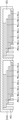
도 1a는 본 발명의 일 실시예에 따른 패키지 유닛(100a)의 단면을 나타낸 측면도이다.1A is a side view showing a cross-section of a
도 1a를 참조하면, 본 발명의 일 태양에 따른 패키지 유닛(100a)은 둘 이상의 적층된 반도체 다이들(110)을 포함할 수 있다. 도 1a에서는 상기 패키지 유닛(100a) 내에 네 개의 반도체 다이들(110a, 110b, 110c, 110d)이 적층된 것으로 도시되었지만, 통상의 기술자는 상기 반도체 다이들(110)이 둘, 셋, 또는 다섯 이상의 반도체 다이들을 포함할 수 있음을 이해할 것이다.Referring to FIG. 1A, a
일부 실시예들에 있어서, 상기 반도체 다이들(110a, 110b, 110c, 110d)은 비휘발성 메모리 장치를 포함할 수 있다. 상기 비휘발성 메모리 장치는, 예를 들면, 플래시 메모리, 상변화 메모리(phase-change RAM, PRAM), 저항 메모리(resistive RAM, RRAM), 강유전체 메모리(ferroelectric RAM, FeRAM), 고체자기 메모리(magnetic RAM, MRAM) 등일 수 있지만 여기에 한정되지 않는다. 상기 플래시 메모리는, 예를 들면 낸드(NAND) 플래시 메모리일 수 있다. 상기 플래시 메모리는, 예를 들면 브이낸드(V-NAND) 플래시 메모리일 수 있다. 상기 비휘발성 메모리 장치는 하나의 반도체 다이로 이루어질 수도 있고, 여러 개의 반도체 다이들이 적층된 것일 수도 있다. In some embodiments, the semiconductor dies 110a, 110b, 110c, and 110d may include a nonvolatile memory device. The nonvolatile memory device includes, for example, a flash memory, a phase-change memory (PRAM), a resistive RAM (RRAM), a ferroelectric memory (FeRAM), and a solid magnetic memory. , MRAM), etc., but is not limited thereto. The flash memory may be, for example, a NAND flash memory. The flash memory may be, for example, a V-NAND flash memory. The nonvolatile memory device may be formed of a single semiconductor die, or may be stacked of several semiconductor dies.
일부 실시예들에 있어서, 상기 반도체 다이들(110a, 110b, 110c, 110d)은 휘발성 메모리 장치를 포함할 수 있다. 상기 휘발성 메모리 장치는 예를 들면, DRAM, SRAM, SDRAM, DDR RAM, RDRAM 등일 수 있지만 여기에 한정되지 않는다. 상기 휘발성 메모리 장치는 상기 외부 호스트가 상기 패키지 유닛(100a)을 액세스할 때 자주 사용되는 데이터를 저장하는 캐시(cache) 기능을 제공하여, 상기 패키지 유닛(100a)과 연결되는 외부 호스트의 프로세스 성능에 맞도록 액세스 시간(access-time)과 데이터 전송 능력(data-transfer performance)을 조정(scale)할 수 있다.In some embodiments, the semiconductor dies 110a, 110b, 110c, and 110d may include a volatile memory device. The volatile memory device may be, for example, DRAM, SRAM, SDRAM, DDR RAM, RDRAM, etc., but is not limited thereto. The volatile memory device provides a cache function for storing frequently used data when the external host accesses the
상기 반도체 다이들(110)은 측방향으로 오프셋(offset)되면서 적층될 수 있다. 다시 말해, 상기 반도체 다이들(110)은 일 방향으로 어긋나면서 계단을 형성하도록 적층될 수 있다. 일부 실시예들에 있어서, 상기 반도체 다이들(110)은 활성면이 상부를 향하도록 하여 적층될 수 있다. 여기서는 상기 반도체 다이들(110)의 상부면이 활성면이고 하부면은 비활성면인 것으로 한다. 상기 반도체 다이들(110)은 활성면들을 부분적으로 노출하도록 오프셋되어 적층될 수 있다.The semiconductor dies 110 may be stacked while being offset in the lateral direction. In other words, the semiconductor dies 110 may be stacked to form steps while being shifted in one direction. In some embodiments, the semiconductor dies 110 may be stacked with an active surface facing upward. Here, it is assumed that the upper surface of the semiconductor dies 110 is an active surface and the lower surface is an inactive surface. The semiconductor dies 110 may be offset and stacked to partially expose active surfaces.
상기 각 반도체 다이들(110a, 110b, 110c, 110d)은 접착제나 다이 부착 필름(die attach film, DAF)과 같은 접착 부재(115)에 의하여 서로 결합될 수 있다. 제 1 접착 부재(115a)는 제 1 반도체 다이(110a)와 제 2 반도체 다이(110b)를 결합할 수 있다. 제 2 접착 부재(115b)는 제 2 반도체 다이(110b)와 제 3 반도체 다이(110c)를 결합할 수 있다. 제 3 접착 부재(115c)는 제 3 반도체 다이(110c)와 제 4 반도체 다이(110d)를 결합할 수 있다. Each of the semiconductor dies 110a, 110b, 110c, and 110d may be bonded to each other by an
상기 반도체 다이들(110)의 측면은 적어도 부분적으로 봉지 물질(120)에 의하여 봉지될 수 있다. 이 때 상기 반도체 다이들(110) 중 적어도 하나는 표면이 노출될 수 있다. 상기 봉지 물질(120)은 에폭시 몰딩 컴파운드(epoxy molding compound, EMC), 감광성 절연막(예컨대 폴리이미드계 물질막), 또는 이들의 조합일 수 있다. 일부 실시예들에 있어서, 상기 반도체 다이들(110)의 일측 측면은 EMC와 접촉하고 다른 일 측면은 감광성 절연막과 접촉할 수 있다. Side surfaces of the semiconductor dies 110 may be at least partially encapsulated by the
구체적으로, 상기 봉지 물질(120)은 제 1 봉지체(124)와 제 2 봉지체(122)를 포함할 수 있다. 상기 제 1 봉지체(124)는 상기 반도체 다이들(110)의 노출된 활성면들을 피복할 수 있다. 상기 제 1 봉지체(124)는 상기 반도체 다이들(110)의 상기 활성면에 각각 평행한 제 1 면(127) 및 제 2 면(128)을 가질 수 있다. 상기 제 2 봉지체(122)는 상기 반도체 다이들(110)의 비활성면과 접촉할 수 있다. Specifically, the
상기 제 1 봉지체(124)와 상기 제 2 봉지체(122)는 서로 상이한 물질일 수 있다. 일부 실시예들에 있어서, 상기 제 1 봉지체(124)는 감광성 절연막일 수 있으며, 예를 들면 감광성을 갖는 폴리이미드계 수지일 수 있다. 일부 실시예들에 있어서, 상기 제 2 봉지체(122)는 비감광성 절연막일 수 있으며, 예를 들면 EMC 수지일 수 있다.The
일부 실시예들에 있어서, 상기 제 1 봉지체(124)는 상기 반도체 다이들(110a, 110b, 110c, 110d) 중 최상위에 위치하는 반도체 다이(110d)의 활성면 전체를 피복할 수 있다.In some embodiments, the
상기 패키지 유닛(100a)에 포함된 각 반도체 다이들(110a, 110b, 110c, 110d)은 패키지 유닛 재배선 라인(130)에 의하여 전기적으로 연결될 수 있다. 일부 실시예들에 있어서, 상기 패키지 유닛 재배선 라인(130)은 둘 이상의 관통 비아(132)와 이들을 연결하는 상부 배선(134)을 포함할 수 있다.Each of the semiconductor dies 110a, 110b, 110c, and 110d included in the
상기 관통 비아(132)는 상기 봉지 물질(120)을 관통하여 각 반도체 다이들(110a, 110b, 110c, 110d)의 활성면에 연결될 수 있다. 일부 실시예들에 있어서, 상기 관통 비아(132)들은 상기 반도체 다이들(110a, 110b, 110c, 110d)이 오프셋되어 노출된 상부 부분에 결합되도록 배치될 수 있다. 일부 실시예들에 있어서, 상기 관통 비아(132)들은 상이한 길이들을 가질 수 있다. 일부 실시예들에 있어서, 상기 관통 비아(132)들의 상단은 실질적으로 동일한 레벨에 위치할 수 있다. 일부 실시예들에 있어서, 상기 관통 비아(132)들은 상기 봉지 물질(120)의 상부 표면으로부터, 각 관통 비아(132)에 대응되는 반도체 다이들(110a, 110b, 110c, 110d)의 상부 표면까지의 거리에 대응되는 수직 길이를 가질 수 있다.The through via 132 may pass through the
일부 실시예들에 있어서, 상기 관통 비아(132)들 중 둘 이상은 상기 봉지 물질(120)의 상부 표면에서 상부 배선(134)에 의하여 서로 연결될 수 있다. 일부 실시예들에 있어서, 상기 반도체 다이들(110a, 110b, 110c, 110d)의 각각에 대응되는 일군의 상기 관통 비아(132)들은 상기 봉지 물질(120)의 상부 표면에서 상부 배선(134)에 의하여 서로 연결될 수 있다. In some embodiments, two or more of the through
상기 상부 배선(134)의 상부에는 캡핑층(135)이 제공될 수 있다. 상기 캡핑층(135)는 예를 들면 실리콘 질화물과 같은 절연체일 수 있다.A
상기 관통 비아(132) 및 상기 상부 배선(134)은 임의의 도전체일 수 있으며 특별히 한정되지 않는다. 예를 들면, 상기 관통 비아(132) 및 상기 상부 배선(134)은 각각 독립적으로, 도핑된 실리콘, 금속, 도전성의 금속 질화물, 도전성의 금속 산화물, 도전성의 금속 산질화물, 또는 이들의 조합일 수 있다. 상기 금속은 티타늄(Ti), 텅스텐(W), 탄탈륨(Ta), 구리(Cu), 알루미늄(Al), 니켈(Ni), 코발트(Co), 철(Fe), 몰리브덴(Mo) 등일 수 있으나 이들에 한정되는 것은 아니다.The through via 132 and the
도 1b는 본 발명의 다른 실시예에 따른 패키지 유닛(100b)의 단면을 나타낸 측면도이다.1B is a side view showing a cross section of a
도 1b를 참조하면, 제 4 반도체 다이(110d)의 상부 표면이 노출되는 것 등을 제외하면 도 1a를 참조하여 설명한 실시예와 실질적으로 동일하다. 따라서 이하에서는 도 1a와의 차이점을 중심으로 설명하고, 도 1a와 동일하거나 유사한 점에 대해서는 구체적인 설명을 생략한다.Referring to FIG. 1B, it is substantially the same as the embodiment described with reference to FIG. 1A except that the upper surface of the
패키지 유닛(100b)에서는 제 1 반도체 다이(110a), 제 2 반도체 다이(110b), 및 제 3 반도체 다이(110c)에 대해서만 대응되는 관통 비아(132a)들이 존재할 수 있다. 상기 관통 비아(132a)들은 상부 배선(134a)을 통하여 상호 연결될 수 있다. 상기 제 4 반도체 다이(110d)는 관통 비아(132a)를 경유하지 않고 상기 상부 배선(134a)과 직접 연결될 수 있다.In the
상기 제 1 봉지체(124)는 상기 반도체 다이들(110a, 110b, 110c, 110d) 중 최상위에 위치하는 반도체 다이인 제 4 반도체 다이(110d)의 활성면 위로는 연장되지 않을 수 있다.The
일부 실시예들에 있어서, 상기 제 1 면(127)은 상기 반도체 다이들(110a, 110b, 110c, 110d) 중 최상위에 위치하는 반도체 다이인 제 4 반도체 다이(110d)의 활성면과 실질적으로 동일 평면 상에 있을 수 있다. 또, 상부 배선들(134a) 중 적어도 하나는 제 1 면(127)으로부터 상기 제 4 반도체 다이(110d)의 활성면 위로 연장될 수 있다. 상기 제 2 면(128)은 상기 반도체 다이들(110a, 110b, 110c, 110d) 중 최하위에 위치하는 반도체 다이인 제 1 반도체 다이(110a)의 비활성면과 실질적으로 동일 평면 상에 있을 수 있다.In some embodiments, the
도 1b에 도시된 패키지 유닛(100b)은 도 1a에 도시된 패키지 유닛(100a)에 비하여 더 얇은 두께를 가질 수 있다.The
도 2a 내지 도 2e는 본 발명의 일 실시예에 따른 패키지 유닛(100a)을 제조하는 방법을 개념적으로 나타낸 측단면도들이다.2A to 2E are side cross-sectional views conceptually showing a method of manufacturing the
도 2a를 참조하면, 캐비티(CA)를 갖는 프레임(101)이 제공된다. 상기 프레임(101)은 소정의 경도를 가진 물질, 예컨대 EMC로 될 수 있으며, 내부에 추후 형성될 반도체 다이들의 적층체가 수용될 수 있는 캐비티(CA)를 가질 수 있다.Referring to FIG. 2A, a
도 2b를 참조하면, 상기 프레임(101)의 캐비티(CA) 내에 제 2 봉지체(122)를 형성한다. 상기 제 2 봉지체(122)는 예를 들면, 프린팅 방식으로 형성될 수 있으며, 예를 들면, 에폭시 몰딩 컴파운드와 같은 폴리머 수지로 될 수 있다. 상기 제 2 봉지체(122)는 추후 배치될 반도체 다이들(110)의 형상에 대응하여 변형 가능할 정도의 점도를 가질 수 있다.Referring to FIG. 2B, a
도 2c를 참조하면, 상기 프레임(101)의 캐비티(CA) 내에 반도체 다이들(110)을 배치한다. 일부 실시예들에 있어서, 상기 반도체 다이들(110)은 제 1 반도체 다이(110a')부터 제 4 반도체 다이(110d)까지 순차 배치될 수 있다. 다른 실시예들에 있어서, 제 1 반도체 다이(110a')부터 제 4 반도체 다이(110d)까지 적층된 적층체를 상기 캐비티 내에 위치시킬 수 있다. 하지만 본 발명이 여기에 한정되는 것은 아니며, 상기 반도체 다이들(110)의 일부를 먼저 상기 캐비티 내에 배치한 후 나머지를 적층시키는 방식으로 배치할 수도 있다.Referring to FIG. 2C, semiconductor dies 110 are disposed in the cavity CA of the
상기 제 1 반도체 다이(110a') 내지 제 4 반도체 다이(110d)는 도 1a를 참조하여 설명한 바와 같이 소정 길이만큼 측방향으로 서로 오프셋되면서 적층될 수 있다.As described with reference to FIG. 1A, the first to fourth semiconductor dies 110a ′ to 110d may be stacked while being laterally offset from each other by a predetermined length.
도 2c에서 보는 바와 같이 상기 제 1 반도체 다이(110a')는 상기 제 2 봉지체(122)의 측면에 밀착되도록 배치될 수 있다. 또한 제 2 반도체 다이(110b)는 상기 제 1 반도체 다이(110a')의 일측 방향으로(도 2c에서는 왼쪽 방향으로) 오프셋되기 때문에 상기 제 2 봉지체(122)의 상부 가장자리와 밀착될 수 있다.As shown in FIG. 2C, the
비록 도 2b 및 도 2c의 실시예에서는 상기 제 2 봉지체(122)가 일시에 제공되고 반도체 다이들(110)의 배치에 의하여 형상이 결정되는 것으로 도시되었지만, 다른 실시예에서는 상기 제 2 봉지체(122)는 반도체 다이들(110)을 적층하면서 각 단계별로 순차 적층될 수도 있다. 본 발명의 다른 실시예에서, 상기 제 2 봉지체(122)는 생략될 수 있다.2B and 2C, the
도 2d를 참조하면, 상기 반도체 다이들(110)의 오프셋된 쪽의 상부 표면을 덮도록 제 1 봉지체(124)가 형성될 수 있다. 상기 제 1 봉지체(124)는 감광성 고분자일 수 있으며, 이 경우 포토리소그래피 방법에 의하여 관통 전극이 형성될 비아홀들(124H)이 용이하게 형성될 수 있다. 상기 감광성 고분자는, 예를 들면, 폴리이미드계 수지일 수 있으나 여기에 한정되는 것은 아니다.Referring to FIG. 2D, a
도 2e를 참조하면, 상기 제 1 봉지체(124)에 형성된 비아홀(124H) 내에 관통 비아(132)를 형성한다. 상기 관통 비아(132)는, 예를 들면, 화학 기상 증착(chemical vapor deposition, CVD), 스퍼터링과 같은 물리 기상 증착(physical vapor deposition, PVD), 전해 도금, 무전해 도금 등의 방법에 의하여 수행될 수 있다. 그러나 본 발명이 여기에 한정되는 것은 아니다.Referring to FIG. 2E, a through via 132 is formed in the via
상기 관통 비아(132)는, 예를 들면, 텅스텐(W), 구리(Cu), 지르코늄(Zr), 티타늄(Ti), 탄탈럼(Ta), 알루미늄(Al), 루테늄(Ru), 팔라듐(Pd), 백금(Pt), 코발트(Co), 니켈(Ni), 또는 이들의 조합으로 이루어질 수 있다. The through via 132 is, for example, tungsten (W), copper (Cu), zirconium (Zr), titanium (Ti), tantalum (Ta), aluminum (Al), ruthenium (Ru), palladium ( It may be made of Pd), platinum (Pt), cobalt (Co), nickel (Ni), or a combination thereof.
상기 관통 비아(132)를 형성하는 공정과 동시에 또는 그러한 공정에 연속하여, 또는 상기 관통 비아(132)를 형성하는 공정과 별도로 상부 배선(134)이 형성될 수 있다. 일부 실시예들에 있어서, 상기 상부 배선(134)은 도전층을 형성한 후 이를 패터닝함으로써 형성될 수 있다. 상기 상부 배선(134)은, 예를 들면, 텅스텐(W), 구리(Cu), 지르코늄(Zr), 티타늄(Ti), 탄탈럼(Ta), 알루미늄(Al), 루테늄(Ru), 팔라듐(Pd), 백금(Pt), 코발트(Co), 니켈(Ni), 또는 이들의 조합으로 이루어질 수 있다. The
이어서 상기 프레임(101)을 제거하고 상기 제 1 반도체 다이(101a')를 일부 두께에 걸쳐 제거하면 도 1a에 도시한 바와 같은 패키지 유닛(100a)을 얻을 수 있다.Subsequently, when the
도 3은 본 발명의 일 실시예에 따른 멀티 스택 패키지(10)를 나타낸 측단면도이다.3 is a side cross-sectional view showing a
도 3을 참조하면, 도 1a에 도시한 패키지 유닛(100a)들이 둘 이상 적층될 수 있다. 도 3에서는 5개의 상기 패키지 유닛(100a)들이 적층된 예가 도시되었지만, 통상의 기술자는 상기 패키지 유닛(100a)들이 둘, 셋, 넷, 또는 여섯 이상 적층될 수 있음을 이해할 것이다.Referring to FIG. 3, two or
복수의 상기 패키지 유닛(100a)들은 적층될 때 상부 배선(134)의 일부가 그의 상부에 배치되는 패키지 유닛(100a)에 의하여 노출되도록 오프셋되도록 배치될 수 있다. 또한 도 3에서는 상기 복수의 패키지 유닛(100a)들이 교대로 좌측 또는 우측으로 오프셋되도록 도시되었지만, 통상의 기술자는 상기 복수의 패키지 유닛(100a)들이 임의의 방향으로 오프셋될 수 있음을 이해할 것이다. 즉, 상기 복수의 패키지 유닛(100a)들은 좌측 또는 우측 방향은 물론, 도 3의 시선 방향의 전면 또는 후면 방향으로도 오프셋될 수 있다.When the plurality of
적층된 복수의 상기 패키지 유닛(100a)들은 패키지 기판(11) 상에 실장될 수 있다. 상기 복수의 상기 패키지 유닛(100a)들은 패키지 기판(11)의 상부 패드(11b)와 본딩 와이어와 같은 연결 수단(15)을 통하여 전기적으로 연결될 수 있다.The stacked plurality of
또한 상기 상부 패드(11b)는 기판 절연체(11a)를 관통하여 연장되는 비아(11d)를 통하여 하부 패드(11c)와 전기적으로 연결되며, 상기 복수의 패키지 유닛(100a)들은 상기 하부 패드(11c)를 통하여 외부 장치와 전기적으로 연결될 수 있다.In addition, the
적층된 상기 복수의 패키지 유닛(100a)들은 몰딩 수지(17)에 의하여 몰딩될 수 있다. 상기 몰딩 수지(17)는 예컨대 EMC일 수 있으나, 본 발명이 여기에 한정되는 것은 아니다.The stacked
도 4a 및 도 4b는 본 발명의 일 실시예에 따른 멀티 스택 패키지(10)의 제조 방법을 나타낸 측단면도들이다.4A and 4B are side cross-sectional views illustrating a method of manufacturing a
도 4a를 참조하면, 적층의 단위가 되는 패키지 유닛(100a)을 제조한다. 상기 패키지 유닛(100a)의 제조는 도 2a 내지 도 2e를 참조하여 설명하였으므로 여기서는 추가적인 설명을 생략한다.Referring to FIG. 4A, a
상기 패키지 유닛(100a)은 추후 적층되기 전에 상기 패키지 유닛(100a)에 대하여 각기 번-인(burn-in) 테스트를 수행할 수 있다. 번-인 테스트를 통과한 양품인 패키지 유닛(100a)만을 선별하여 추후 적층에 사용할 수 있다.Each of the
도 4b를 참조하면, 패키지 기판(11) 위에 복수의 패키지 유닛(100a)들을 적층한다. 이 때 도 3을 참조하여 설명한 바와 같이 적층되는 패키지 유닛(100a)들이 서로 오프셋되도록 상기 패키지 기판(11) 상에 적층할 수 있다. 보다 구체적으로, 상기 복수의 패키지 유닛(100a)들은 적층될 때 상부 배선(134)의 일부가 그의 상부에 배치되는 패키지 유닛(100a)에 의하여 노출되도록 오프셋되도록 배치될 수 있다. Referring to FIG. 4B, a plurality of
하나의 패키지 유닛(100a)과 그 위의 패키지 유닛(100a)은 다이 부착 필름(DAF)과 같은 접착 부재에 의하여 서로 결합될 수 있다.One
그런 다음 노출된 상기 상부 배선(134)을 상기 패키지 기판(11)의 상부 패드(11b)와 전기적으로 연결한다. 상기 상부 배선(134)은, 예를 들면, 본딩 와이어와 같은 연결 수단(15)에 의하여 상부 패드(11b)에 전기적으로 연결될 수 있다.Then, the exposed
이어서 상기 복수의 패키지 유닛(100a)들이 적층된 적층체를 몰딩 수지(17)로 몰딩하면 본 발명의 일 실시예에 따른 멀티 스택 패키지(10)를 얻을 수 있다.Subsequently, when the laminate in which the plurality of
본 발명의 실시예들에 따르면 각 패키지 유닛들을 개별적으로 번-인(burn-in) 테스트한 후 양품으로 판정된 패키지 유닛들을 이용하여 멀티스택 패키지를 제조하기 때문에 멀티 스택 패키지 전체가 불량으로 판정되는 가능성을 크게 낮출 수 있다. 종래에는 전체 반도체 다이들이 실장된 전체 패키지의 제조를 완료한 후 번-인 테스트를 수행하였기 때문에 하나의 반도체 다이라도 불량이 있는 경우에는 전체 반도체 패키지가 모두 불량으로 판정나서 수율 손실(yield loss)이 증대되는 문제점이 있었다.According to embodiments of the present invention, since each package unit is individually burn-in tested and then a multi-stack package is manufactured using package units determined as good products, the entire multi-stack package is determined as defective. It can greatly reduce the likelihood. Conventionally, since the burn-in test was performed after manufacturing the entire package with all the semiconductor dies mounted, if all of the semiconductors are defective, the entire semiconductor package is judged as defective, resulting in a yield loss. There was an increasing problem.
도 5a 내지 도 5f는 본 발명의 다른 실시예에 따른 패키지 유닛(100c)의 제조 방법을 나타낸 측단면도들이다.5A to 5F are side cross-sectional views illustrating a method of manufacturing a
도 5a 내지 도 5f에 도시한 제조 방법은 도 2a 내지 도 2e를 참조하여 설명한 실시예와 대비하여 둘 이상의 패키지 유닛이 동시에 제조되는 점에서 차이가 있다. 따라서 이하에서는 상기 차이점을 중심으로 설명하고 공통되는 부분에 대해서는 설명을 생략한다.The manufacturing method illustrated in FIGS. 5A to 5F is different from the embodiment described with reference to FIGS. 2A to 2E in that two or more package units are simultaneously manufactured. Therefore, in the following description, the differences will be mainly described, and descriptions of common parts will be omitted.
도 5a를 참조하면, 복수의 캐비티들(CA)이 형성된 프레임(101C)이 제공된다. 상기 프레임(101C)은 복수의 캐비티들(CA)을 둘 이상 가질 수 있다. 도 5a에서는 프레임(101C)에 두 개의 캐비티들(CA)이 형성된 예를 도시하였지만, 통상의 기술자는 프레임(101C)에 셋 이상의 캐비티들(CA)이 형성될 수 있음을 이해할 것이다.Referring to FIG. 5A, a
도 5b 내지 도 5e에 나타낸 단계들은 각각 도 2b 내지 도 2e에 나타낸 단계들과 실질적으로 동일하므로 여기서는 간략하게 설명한다.Since the steps shown in FIGS. 5B to 5E are substantially the same as the steps shown in FIGS. 2B to 2E, respectively, a brief description will be given here.
도 5b를 참조하면, 프레임(101C)의 캐비티(CA)들 내에 제 2 봉지체(122)를 각각 형성한다. 도 5c를 참조하면, 상기 프레임(101C)의 캐비티(CA)들 내에 반도체 다이들(110a', 110b, 110c, 110d)을 각각 배치한다. 도 5d를 참조하면, 상기 반도체 다이들(110a', 110b, 110c, 110d)의 오프셋된 쪽의 상부 표면을 덮도록 감광성 고분자를 포함하는 제 1 봉지체(124)를 형성하고 비아홀들을 형성한다. 도 5e를 참조하면, 상기 비아홀 내에 관통 비아(132)를 형성한다.Referring to FIG. 5B, the
도 5f를 참조하면, 제 1 반도체 다이(110a)를 노출시키기 위하여 도 5e의 LH 선을 따라 그라인딩을 수행할 수 있다. 또한, 각 패키지 유닛(100c)을 개별화(singulation)하기 위하여 도 5e의 LV 선을 따라 쏘잉(sawing)을 수행할 수 있다.Referring to FIG. 5F, grinding may be performed along the line LH of FIG. 5E to expose the
그 결과로서 얻어지는 패키지 유닛(100c)은 측표면 상에 상기 프레임(101C)의 일부분인 프레임 잔여부(101R)가 잔존하게 된다. 상기 프레임 잔여부(101R)는 상기 패키지 유닛(100c)의 측면들의 전부 또는 일부를 피복할 수 있다. 일부 실시예들에 있어서, 상기 프레임 잔여부(101R)는 상기 패키지 유닛(100c)의 각 측면들을 적어도 부분적으로 피복할 수 있다. 일부 실시예들에 있어서, 상기 프레임 잔여부(101R)는 제 1 봉지체(124) 및/또는 제 2 봉지체(122) 중 적어도 하나의 측면 상에 잔존할 수 있다.In the
도 6a 내지 도 6f는 본 발명의 또 다른 실시예에 따른 패키지 유닛(100c)의 제조 방법을 나타낸 측단면도들이다.6A to 6F are side cross-sectional views illustrating a method of manufacturing a
도 6a 내지 도 6f에 도시한 제조 방법은 도 5a 내지 도 5f를 참조하여 설명한 실시예와 대비하여 복수의 캐비티들이 프레임(101S)을 관통하도록 형성되는 점에서 차이가 있다. 따라서 이하에서는 상기 차이점을 중심으로 설명하고 공통되는 부분에 대해서는 설명을 생략한다.The manufacturing method shown in FIGS. 6A to 6F is different from the embodiment described with reference to FIGS. 5A to 5F in that a plurality of cavities are formed to penetrate the
도 6a를 참조하면 복수의 캐비티들이 형성된 프레임(100S)이 제공된다. 상기 프레임(101S)은 복수의 캐비티들을 둘 이상 가질 수 있다. 도 6a에서는 프레임(101S)에 두 개의 캐비티들이 형성된 예를 도시하였지만, 통상의 기술자는 프레임(101S)에 셋 이상의 캐비티들이 형성될 수 있음을 이해할 것이다.Referring to FIG. 6A, a frame 100S in which a plurality of cavities are formed is provided. The
상기 캐비티들 각각의 면적과 높이는 추후 설명되는 바와 같이 그 안에 실장되는 반도체 다이들의 크기와 수를 고려하여 결정될 수 있다. As will be described later, the area and height of each of the cavities may be determined in consideration of the size and number of semiconductor dies mounted therein.
도 6b 내지 도 6e에 나타낸 단계들은 각각 도 2b 내지 도 2e에 나타낸 단계들과 실질적으로 동일하므로 여기서는 간략하게 설명한다.Since the steps shown in FIGS. 6B to 6E are substantially the same as the steps shown in FIGS. 2B to 2E, respectively, a brief description will be given here.
도 6b를 참조하면, 프레임(101S)의 캐비티(CA)들 내에 제 2 봉지체(122)를 각각 형성한다. 도 6c를 참조하면, 상기 프레임(101S)의 캐비티(CA)들 내에 반도체 다이들(110a', 110b, 110c, 110d)을 각각 배치한다. 도 6d를 참조하면, 상기 반도체 다이들(110a', 110b, 110c, 110d)의 오프셋된 쪽의 상부 표면을 덮도록 감광성 고분자를 포함하는 제 1 봉지체(124)를 형성하고 비아홀들을 형성한다. 도 6e를 참조하면, 상기 비아홀 내에 관통 비아(132)를 형성한다.Referring to FIG. 6B, the
도 6f를 참조하면, 각 패키지 유닛(100c)을 개별화(singulation)하기 위하여 도 6e의 LV 선을 따라 쏘잉을 수행할 수 있다.Referring to FIG. 6F, in order to singulate each
그 결과로서 얻어지는 패키지 유닛(100c)은 도 5f에서 얻어지는 패키지 유닛(100c)과 동일할 수 있다. 도 6a 내지 도 6f에 나타낸 실시예에서는 도 5e의 LH 선을 따라 그라인딩을 할 필요가 없기 때문에 공정이 더욱 간단하다. 또한 적층에 사용되는 반도체 다이들의 두께가 모두 동일할 수 있기 때문에 제조 비용이 절감될 수 있다.The
도 7a 내지 도 7e는 본 발명의 또 다른 실시예에 따른 패키지 유닛의 제조 방법을 나타낸 측단면도들이다.7A to 7E are side cross-sectional views illustrating a method of manufacturing a package unit according to still another embodiment of the present invention.
도 7a 내지 도 7e에 도시한 제조 방법은 도 5a 내지 도 5f를 참조하여 설명한 실시예와 대비하여 프레임(101D)의 캐비티(CA) 내에 반도체 다이들이 오프셋되면서 안착될 수 있는 스텝 형상의 안착부(101SP)가 구비된 점에서 차이가 있다. 따라서 이하에서는 상기 차이점을 중심으로 설명하고 공통되는 부분에 대해서는 설명을 생략한다.The manufacturing method shown in FIGS. 7A to 7E is a step-shaped seating portion in which semiconductor dies are offset and seated in the cavity CA of the
도 7a를 참조하면, 상기 프레임(101D) 내에는 스텝 형상의 안착부(101SP)가 구비될 수 있다. 상기 안착부(101SP)는 상기 프레임(101D)과 별도로 형성될 수도 있고 상기 프레임(101D)과 일체로 형성될 수도 있다.Referring to FIG. 7A, a step-shaped seating portion 101SP may be provided in the
도 7b를 참조하면, 상기 프레임(101D) 내에 복수의 반도체 다이들(110a', 110b, 110c, 110d)이 순차 적층될 수 있으며, 상기 반도체 다이들(110a', 110b, 110c, 110d)의 각 높이와 접착 부재(115a, 115b, 115c)의 높이의 합이 상기 안착부(101SP)의 높이가 될 수 있다.Referring to FIG. 7B, a plurality of semiconductor dies 110a', 110b, 110c, and 110d may be sequentially stacked in the
도 7b 내지 도 7e에 나타낸 단계들은 각각 도 5c 내지 도 5f에 나타낸 단계들과 실질적으로 동일하므로 여기서는 간략하게 설명한다.Since the steps shown in FIGS. 7B to 7E are substantially the same as the steps shown in FIGS. 5C to 5F, respectively, a brief description will be given here.
도 7b를 참조하면, 상기 프레임(101D)의 캐비티(CA)들 내에 반도체 다이들(110a', 110b, 110c, 110d)을 각각 배치한다. 도 7c를 참조하면, 상기 반도체 다이들(110a', 110b, 110c, 110d)의 오프셋된 쪽의 상부 표면을 덮도록 감광성 고분자를 포함하는 제 1 봉지체(124)를 형성하고 비아홀들을 형성한다. 도 7d를 참조하면, 상기 비아홀 내에 관통 비아(132)를 형성한다. 도 7e를 참조하면, 제 1 반도체 다이(110a)를 노출시키기 위하여 도 7d의 LH 선을 따라 그라인딩을 수행할 수 있다. 또한, 각 패키지 유닛(100d)을 개별화(singulation)하기 위하여 도 7d의 LV 선을 따라 쏘잉(sawing)을 수행할 수 있다.Referring to FIG. 7B, semiconductor dies 110a', 110b, 110c, and 110d are disposed in the cavities CA of the
도 8a 내지 도 8d는 본 발명의 또 다른 실시예에 따른 패키지 유닛의 제조 방법을 나타낸 측단면도들이다.8A to 8D are side cross-sectional views illustrating a method of manufacturing a package unit according to still another embodiment of the present invention.
도 8a를 참조하면, 배선들(232, 234)이 형성된 프레임(224)이 제공된다. 상기 배선들(232, 234)은 프레임(224)에 홀을 형성한 후 도금, 증착 등의 방법을 이용하여 형성할 수 있다.Referring to FIG. 8A, a
도 8b를 참조하면, 상기 프레임(224) 내의 각 스텝에 노출된 수직 배선(232) 상에 접속 수단(237')을 배치할 수 있다. 상기 접속 수단(237')은 솔더볼이 예시될 수 있지만 여기에 한정되는 것은 아니다. Referring to FIG. 8B, a connection means 237 ′ may be disposed on the
그런 다음 제 1 반도체 다이(210a)를 상기 프레임(224) 내에 배치할 수 있다. 이 때 상기 제 1 반도체 다이(210a)를 상기 프레임(224)에 부착시키는 접착 부재(215a)가 상기 제 1 반도체 다이(210a)와 상기 프레임(224) 사이에 개재될 수 있다. 상기 접착 부재(215a)는 다이 부착 필름, 비전도성 필름(non-conductive film, NCF), 이방성 도전 필름(anisotropic conductive film, ACF) 등일 수 있지만 이들에 한정되는 것은 아니다. 특히, ACF가 사용되는 경우 상기 접속 수단(237')은 생략될 수 있다.Then, the
도 8c를 참조하면, 제 1 내지 제 4 반도체 다이(210a, 210b, 210c, 210d)가 순차 부착될 수 있다.Referring to FIG. 8C, first to fourth semiconductor dies 210a, 210b, 210c, and 210d may be sequentially attached.
도 8d를 참조하면, 상기 제 1 내지 제 4 반도체 다이(210a, 210b, 210c, 210d)를 봉지재(220)로 봉지(encapsulation)한다. 상기 봉지재(220)는 예를 들면, EMC와 같은 물질일 수 있지만 여기에 한정되는 것은 아니다.Referring to FIG. 8D, the first to fourth semiconductor dies 210a, 210b, 210c, and 210d are encapsulated with an
본 발명의 실시예들에 따른 패키지 유닛들을 이용하여 멀티 스택 패키지를 제조하면 신속하게 제조할 수 있을 뿐만 아니라 번-인 테스트한 패키지 유닛들 중 불량인 패키지 유닛을 미리 배제할 수 있기 때문에 멀티 스택 패키지 전체가 불량으로 판정되는 가능성을 크게 낮출 수 있다. 종래에는 전체 반도체 다이들이 실장된 전체 패키지의 제조를 완료한 후 번-인 테스트를 수행하였기 때문에 하나의 반도체 다이라도 불량이 있는 경우에는 전체 반도체 패키지가 모두 불량으로 판정나서 수율 손실(yield loss)이 증대되는 문제점이 있었다.If a multi-stack package is manufactured using the package units according to the embodiments of the present invention, not only can it be manufactured quickly, but also a defective package unit among the package units tested for burn-in can be excluded in advance. The possibility that the whole is judged as defective can be greatly reduced. Conventionally, since the burn-in test was performed after manufacturing the entire package with all the semiconductor dies mounted, if all of the semiconductors are defective, the entire semiconductor package is judged as defective, resulting in a yield loss. There was an increasing problem.
또한, 본원 발명은 다수의 반도체 다이들을 순차적으로 적층하는 것이 아니라, 이미 복수의 반도체 다이들(도 1a에서는 4 개의 반도체 다이들)이 적층된 패키지 유닛을 적층하기 때문에 제조가 간단하고 신속하며 비용이 저렴하다.In addition, the present invention does not stack a plurality of semiconductor dies sequentially, but stacks a package unit in which a plurality of semiconductor dies (four semiconductor dies in FIG. 1A) are stacked, so that manufacturing is simple, fast, and cost-effective It is cheaper.
이상에서 살펴본 바와 같이 본 발명의 실시예들에 대해 상세히 기술되었지만, 본 발명이 속하는 기술분야에 있어서 통상의 지식을 가진 사람이라면, 첨부된 청구 범위에 정의된 본 발명의 정신 및 범위를 벗어나지 않으면서 본 발명을 여러 가지로 변형하여 실시할 수 있을 것이다. 따라서 본 발명의 앞으로의 실시예들의 변경은 본 발명의 기술을 벗어날 수 없을 것이다.Although described in detail with respect to the embodiments of the present invention as described above, those of ordinary skill in the art to which the present invention belongs, without departing from the spirit and scope of the present invention defined in the appended claims It will be possible to practice the present invention by various modifications. Therefore, changes to the embodiments of the present invention will not be able to depart from the technology of the present invention.
Claims (13)
상기 복수의 반도체 다이들의 노출된 상기 활성면을 피복하고, 상기 활성면에 평행한 제 1 면 및 제 2 면을 갖고, 감광성 절연막을 포함하는 제 1 봉지체;
상기 제 1 봉지체와 상이하고, 상기 비활성면과 접촉하며 상기 복수의 반도체 다이들을 피복하는 제 2 봉지체;
상기 제 1 면으로부터 상기 제 1 봉지체를 관통하여 상기 활성면까지 연장되는 관통 비아들; 및
상기 제 1 봉지체의 제 1 면 위에서 상기 관통 비아들을 연결하는 상부 배선들;
을 포함하고,
상기 제 1 봉지체의 상기 제 2 면은 최하위에 위치하는 반도체 다이의 상기 비활성면 및 상기 제 2 봉지체의 최하면과 동일 평면 위에 있는 패키지 유닛.A plurality of semiconductor dies each including an active surface and a non-active surface opposite to the active surface, and offset and stacked to partially expose the active surfaces;
A first encapsulation member covering the exposed active surface of the plurality of semiconductor dies, having first and second surfaces parallel to the active surface, and including a photosensitive insulating film;
A second encapsulation member different from the first encapsulation member, contacting the inactive surface, and covering the plurality of semiconductor dies;
Through vias extending from the first surface to the active surface through the first encapsulation member; And
Upper wirings connecting the through vias on a first surface of the first encapsulation member;
Including,
The second surface of the first encapsulation member is on the same plane as the inactive surface of the semiconductor die and the lowermost surface of the second encapsulation member.
상기 감광성 절연막이 폴리이미드계 수지인 것을 특징으로 하는 패키지 유닛.The method of claim 1,
The package unit, wherein the photosensitive insulating film is a polyimide resin.
상기 복수의 반도체 다이들 중 최상위에 위치하는 반도체 다이의 상부면 전체를 상기 제 1 봉지체가 피복하는 것을 특징으로 하는 패키지 유닛.The method of claim 1,
And the first encapsulant covers the entire upper surface of the semiconductor die positioned at the top of the plurality of semiconductor dies.
상기 제 2 봉지체는 에폭시 몰딩 컴파운드(epoxy molding compound, EMC)를 포함하는 것을 특징으로 하는 패키지 유닛.The method of claim 1,
The second encapsulant comprises an epoxy molding compound (EMC).
상기 복수의 반도체 다이들의 노출된 상기 활성면을 피복하고, 상기 활성면에 평행한 제 1 면 및 제 2 면을 갖고, 감광성 절연막을 포함하는 제 1 봉지체;
상기 제 1 봉지체와 상이하고, 상기 비활성면과 접촉하며 상기 복수의 반도체 다이들을 피복하는 제 2 봉지체;
상기 제 1 면으로부터 상기 제 1 봉지체를 관통하여 상기 활성면까지 연장되는 관통 비아들; 및
상기 제 1 봉지체의 제 1 면 위에서 상기 관통 비아들을 연결하는 상부 배선들;
을 포함하고,
상기 제 1 봉지체 및 상기 제 2 봉지체 중 적어도 하나의 측면 상에 프레임 잔여부를 더 포함하는 것을 특징으로 하는 패키지 유닛.A plurality of semiconductor dies each including an active surface and a non-active surface opposite to the active surface, and offset and stacked to partially expose the active surfaces;
A first encapsulation member covering the exposed active surface of the plurality of semiconductor dies, having first and second surfaces parallel to the active surface, and including a photosensitive insulating film;
A second encapsulation member different from the first encapsulation member, contacting the inactive surface, and covering the plurality of semiconductor dies;
Through vias extending from the first surface to the active surface through the first encapsulation member; And
Upper wirings connecting the through vias on a first surface of the first encapsulation member;
Including,
The package unit, further comprising a frame residual portion on at least one side of the first and second encapsulation bodies.
상기 제 1 봉지체는 최상위에 위치하는 반도체 다이의 활성면 위로는 연장되지 않는 것을 특징으로 하는 패키지 유닛.The method according to claim 1 or 7,
Wherein the first encapsulant does not extend above the active surface of the uppermost semiconductor die.
상기 제 1 봉지체의 제 1 면은 상기 최상위에 위치하는 반도체 다이의 상기 활성면과 동일 평면 위에 있고,
상기 상부 배선들 중 적어도 하나의 상부 배선은 상기 제 1 면 위로부터 상기 활성면 위로 연장되는 것을 특징으로 하는 패키지 유닛.The method of claim 8,
The first surface of the first encapsulant is on the same plane as the active surface of the uppermost semiconductor die,
The package unit, wherein at least one of the upper wirings extends from the first surface to the active surface.
상기 패키지 기판 위에 적층된 둘 이상의 제 1 항 또는 제 7 항에 따른 패키지 유닛들; 및
상기 패키지 유닛들을 봉지하는 몰딩 수지;
를 포함하는 멀티 스택 패키지.Package substrate;
Two or more package units according to claim 1 or 7 stacked on the package substrate; And
A molding resin encapsulating the package units;
A multi-stack package containing.
상기 캐비티 내에 복수의 반도체 다이들을 적층하되, 상기 반도체 다이들 각각의 활성면들이 부분적으로 노출되도록 상기 반도체 다이들을 오프셋 방식으로 적층하는 단계;
상기 반도체 다이들이 오프셋됨으로써 노출된 상기 활성면들을 덮도록 감광성 고분자를 포함하는 제 2 봉지체를 형성하는 단계;
포토리소그래피 방식으로 상기 제 2 봉지체에 상기 활성면을 노출시키는 관통 비아홀들을 형성하는 단계;
상기 관통 비아홀들 내에 관통 비아들을 형성하는 단계;
상기 제 2 봉지체의 상부면에 상기 관통 비아들을 연결하는 상부 배선을 형성하는 단계;
를 포함하는 패키지 유닛의 제조 방법.Forming a first encapsulant in the cavity of the frame;
Stacking a plurality of semiconductor dies in the cavity, and stacking the semiconductor dies in an offset manner so that active surfaces of each of the semiconductor dies are partially exposed;
Forming a second encapsulant including a photosensitive polymer to cover the exposed active surfaces by offsetting the semiconductor dies;
Forming through via holes exposing the active surface to the second encapsulant by a photolithography method;
Forming through vias in the through via holes;
Forming an upper wiring connecting the through vias on an upper surface of the second encapsulant;
A method of manufacturing a package unit comprising a.
상기 제 1 봉지체는 감광성 고분자를 포함하지 않는 것을 특징으로 하는 패키지 유닛의 제조 방법.The method of claim 11,
The method of manufacturing a package unit, wherein the first encapsulant does not contain a photosensitive polymer.
상기 제 2 봉지체를 형성하는 단계는 상기 복수의 반도체 다이들 중 최상위에 위치하는 반도체 다이의 상부면 전체를 상기 제 2 봉지체가 피복하는 단계를 포함하는 것을 특징으로 하는 패키지 유닛의 제조 방법.
The method of claim 11,
The forming of the second encapsulant includes the step of covering the entire upper surface of the semiconductor die positioned at the top of the plurality of semiconductor dies with the second encapsulant.
Applications Claiming Priority (2)
| Application Number | Priority Date | Filing Date | Title |
|---|---|---|---|
| KR1020180056170 | 2018-05-16 | ||
| KR20180056170 | 2018-05-16 |
Publications (2)
| Publication Number | Publication Date |
|---|---|
| KR20190131453A KR20190131453A (en) | 2019-11-26 |
| KR102173811B1 true KR102173811B1 (en) | 2020-11-04 |
Family
ID=68731489
Family Applications (1)
| Application Number | Title | Priority Date | Filing Date |
|---|---|---|---|
| KR1020190057602A Active KR102173811B1 (en) | 2018-05-16 | 2019-05-16 | Package unit and multi-stack package |
Country Status (1)
| Country | Link |
|---|---|
| KR (1) | KR102173811B1 (en) |
Families Citing this family (1)
| Publication number | Priority date | Publication date | Assignee | Title |
|---|---|---|---|---|
| CN111048479B (en) * | 2019-12-27 | 2021-06-29 | 华天科技(南京)有限公司 | A multi-chip stack packaging structure and packaging method thereof |
Family Cites Families (4)
| Publication number | Priority date | Publication date | Assignee | Title |
|---|---|---|---|---|
| US20100193930A1 (en) * | 2009-02-02 | 2010-08-05 | Samsung Electronics Co., Ltd. | Multi-chip semiconductor devices having conductive vias and methods of forming the same |
| KR101686553B1 (en) * | 2010-07-12 | 2016-12-14 | 삼성전자 주식회사 | Chip Stacked Package and Package on Package |
| US10049953B2 (en) * | 2015-09-21 | 2018-08-14 | Taiwan Semiconductor Manufacturing Company, Ltd. | Method of manufacturing an integrated fan-out package having fan-out redistribution layer (RDL) to accommodate electrical connectors |
| KR20180001699A (en) * | 2016-06-27 | 2018-01-05 | 에스케이하이닉스 주식회사 | Methods for fabricating wafer level package and wafer level package fabricated thereby |
-
2019
- 2019-05-16 KR KR1020190057602A patent/KR102173811B1/en active Active
Also Published As
| Publication number | Publication date |
|---|---|
| KR20190131453A (en) | 2019-11-26 |
Similar Documents
| Publication | Publication Date | Title |
|---|---|---|
| US8803334B2 (en) | Semiconductor package including a semiconductor chip with a through silicon via | |
| US8847378B2 (en) | Semiconductor package | |
| US10262967B2 (en) | Semiconductor packages | |
| US20150200186A1 (en) | Electronic device, semiconductor package, and method of manufacturing the same | |
| US9911688B2 (en) | Semiconductor chip, semiconductor package including the same, and method of fabricating the same | |
| US20180122789A1 (en) | Semiconductor package and method of manufacturing the semiconductor package | |
| US8455349B2 (en) | Layered chip package and method of manufacturing same | |
| KR102434988B1 (en) | Semiconductor package and manufacturing method thereof | |
| US11094636B2 (en) | Semiconductor package and method of manufacturing the semiconductor package | |
| US11239219B2 (en) | Passive device module and semiconductor package including the same | |
| US20130075905A1 (en) | Semiconductor Chips and Semiconductor Packages and Methods of Fabricating the Same | |
| US20240332198A1 (en) | Semiconductor device and semiconductor package including the same | |
| US20250070094A1 (en) | Semiconductor package | |
| US20260020232A1 (en) | Semiconductor package having stacked interconnected semiconductor chips | |
| US20130037946A1 (en) | Semiconductor chip including bump having barrier layer, and manufacturing method thereof | |
| US10090266B2 (en) | Semiconductor device, and method of fabricating the same | |
| KR102173811B1 (en) | Package unit and multi-stack package | |
| KR20230033996A (en) | Semiconductor package | |
| KR102905973B1 (en) | Semiconductor package | |
| KR20200115298A (en) | Semiconductor package | |
| US20240071996A1 (en) | Semiconductor package and method of manufacturing the semiconductor package | |
| US11502053B2 (en) | Bond pad connection layout | |
| US11652090B2 (en) | Semiconductor package and method for fabricating the same | |
| US20250149507A1 (en) | Semiconductor package including encapsulation layers | |
| US20240136262A1 (en) | Semiconductor package and method for fabricating the same |
Legal Events
| Date | Code | Title | Description |
|---|---|---|---|
| PA0109 | Patent application |
St.27 status event code: A-0-1-A10-A12-nap-PA0109 |
|
| A201 | Request for examination | ||
| PA0201 | Request for examination |
St.27 status event code: A-1-2-D10-D11-exm-PA0201 |
|
| P11-X000 | Amendment of application requested |
St.27 status event code: A-2-2-P10-P11-nap-X000 |
|
| P13-X000 | Application amended |
St.27 status event code: A-2-2-P10-P13-nap-X000 |
|
| D13-X000 | Search requested |
St.27 status event code: A-1-2-D10-D13-srh-X000 |
|
| PG1501 | Laying open of application |
St.27 status event code: A-1-1-Q10-Q12-nap-PG1501 |
|
| D14-X000 | Search report completed |
St.27 status event code: A-1-2-D10-D14-srh-X000 |
|
| E902 | Notification of reason for refusal | ||
| PE0902 | Notice of grounds for rejection |
St.27 status event code: A-1-2-D10-D21-exm-PE0902 |
|
| E13-X000 | Pre-grant limitation requested |
St.27 status event code: A-2-3-E10-E13-lim-X000 |
|
| P11-X000 | Amendment of application requested |
St.27 status event code: A-2-2-P10-P11-nap-X000 |
|
| P13-X000 | Application amended |
St.27 status event code: A-2-2-P10-P13-nap-X000 |
|
| E701 | Decision to grant or registration of patent right | ||
| PE0701 | Decision of registration |
St.27 status event code: A-1-2-D10-D22-exm-PE0701 |
|
| GRNT | Written decision to grant | ||
| PR0701 | Registration of establishment |
St.27 status event code: A-2-4-F10-F11-exm-PR0701 |
|
| PR1002 | Payment of registration fee |
St.27 status event code: A-2-2-U10-U11-oth-PR1002 Fee payment year number: 1 |
|
| PG1601 | Publication of registration |
St.27 status event code: A-4-4-Q10-Q13-nap-PG1601 |
|
| R18-X000 | Changes to party contact information recorded |
St.27 status event code: A-5-5-R10-R18-oth-X000 |
|
| PR1001 | Payment of annual fee |
St.27 status event code: A-4-4-U10-U11-oth-PR1001 Fee payment year number: 4 |
|
| R17-X000 | Change to representative recorded |
St.27 status event code: A-5-5-R10-R17-oth-X000 |
|
| PR1001 | Payment of annual fee |
St.27 status event code: A-4-4-U10-U11-oth-PR1001 Fee payment year number: 5 |
|
| P22-X000 | Classification modified |
St.27 status event code: A-4-4-P10-P22-nap-X000 |
|
| P22-X000 | Classification modified |
St.27 status event code: A-4-4-P10-P22-nap-X000 |