KR102116829B1 - Uv light emitting diode and method of fabricating the same - Google Patents
Uv light emitting diode and method of fabricating the same Download PDFInfo
- Publication number
- KR102116829B1 KR102116829B1 KR1020130145122A KR20130145122A KR102116829B1 KR 102116829 B1 KR102116829 B1 KR 102116829B1 KR 1020130145122 A KR1020130145122 A KR 1020130145122A KR 20130145122 A KR20130145122 A KR 20130145122A KR 102116829 B1 KR102116829 B1 KR 102116829B1
- Authority
- KR
- South Korea
- Prior art keywords
- layer
- well
- based semiconductor
- light emitting
- layers
- Prior art date
- Legal status (The legal status is an assumption and is not a legal conclusion. Google has not performed a legal analysis and makes no representation as to the accuracy of the status listed.)
- Active
Links
- 238000004519 manufacturing process Methods 0.000 title claims abstract description 25
- 230000004888 barrier function Effects 0.000 claims abstract description 111
- 150000004767 nitrides Chemical class 0.000 claims abstract description 105
- 239000004065 semiconductor Substances 0.000 claims abstract description 102
- 239000000203 mixture Substances 0.000 claims abstract description 84
- 230000003750 conditioning effect Effects 0.000 claims abstract description 56
- 229910002704 AlGaN Inorganic materials 0.000 claims description 41
- 239000000758 substrate Substances 0.000 claims description 23
- 238000000034 method Methods 0.000 claims description 22
- 239000010410 layer Substances 0.000 description 391
- 235000012431 wafers Nutrition 0.000 description 20
- 229910002601 GaN Inorganic materials 0.000 description 11
- 230000000052 comparative effect Effects 0.000 description 9
- 230000003287 optical effect Effects 0.000 description 9
- 238000005424 photoluminescence Methods 0.000 description 8
- 230000007547 defect Effects 0.000 description 4
- 229910052594 sapphire Inorganic materials 0.000 description 4
- 239000010980 sapphire Substances 0.000 description 4
- JMASRVWKEDWRBT-UHFFFAOYSA-N Gallium nitride Chemical compound [Ga]#N JMASRVWKEDWRBT-UHFFFAOYSA-N 0.000 description 2
- 239000013078 crystal Substances 0.000 description 2
- 238000009826 distribution Methods 0.000 description 2
- 239000002356 single layer Substances 0.000 description 2
- 239000000443 aerosol Substances 0.000 description 1
- 229910052782 aluminium Inorganic materials 0.000 description 1
- 238000005452 bending Methods 0.000 description 1
- 238000005229 chemical vapour deposition Methods 0.000 description 1
- 238000007796 conventional method Methods 0.000 description 1
- PMHQVHHXPFUNSP-UHFFFAOYSA-M copper(1+);methylsulfanylmethane;bromide Chemical compound Br[Cu].CSC PMHQVHHXPFUNSP-UHFFFAOYSA-M 0.000 description 1
- 230000000694 effects Effects 0.000 description 1
- 230000005284 excitation Effects 0.000 description 1
- 238000001917 fluorescence detection Methods 0.000 description 1
- 229910052733 gallium Inorganic materials 0.000 description 1
- 229910052738 indium Inorganic materials 0.000 description 1
- 229910052751 metal Inorganic materials 0.000 description 1
- 239000002184 metal Substances 0.000 description 1
- 230000001954 sterilising effect Effects 0.000 description 1
- 238000004659 sterilization and disinfection Methods 0.000 description 1
Images


Classifications
-
- H—ELECTRICITY
- H10—SEMICONDUCTOR DEVICES; ELECTRIC SOLID-STATE DEVICES NOT OTHERWISE PROVIDED FOR
- H10H—INORGANIC LIGHT-EMITTING SEMICONDUCTOR DEVICES HAVING POTENTIAL BARRIERS
- H10H20/00—Individual inorganic light-emitting semiconductor devices having potential barriers, e.g. light-emitting diodes [LED]
- H10H20/80—Constructional details
- H10H20/81—Bodies
- H10H20/822—Materials of the light-emitting regions
- H10H20/824—Materials of the light-emitting regions comprising only Group III-V materials, e.g. GaP
- H10H20/825—Materials of the light-emitting regions comprising only Group III-V materials, e.g. GaP containing nitrogen, e.g. GaN
-
- H—ELECTRICITY
- H10—SEMICONDUCTOR DEVICES; ELECTRIC SOLID-STATE DEVICES NOT OTHERWISE PROVIDED FOR
- H10H—INORGANIC LIGHT-EMITTING SEMICONDUCTOR DEVICES HAVING POTENTIAL BARRIERS
- H10H20/00—Individual inorganic light-emitting semiconductor devices having potential barriers, e.g. light-emitting diodes [LED]
- H10H20/80—Constructional details
- H10H20/81—Bodies
- H10H20/811—Bodies having quantum effect structures or superlattices, e.g. tunnel junctions
- H10H20/812—Bodies having quantum effect structures or superlattices, e.g. tunnel junctions within the light-emitting regions, e.g. having quantum confinement structures
-
- H—ELECTRICITY
- H10—SEMICONDUCTOR DEVICES; ELECTRIC SOLID-STATE DEVICES NOT OTHERWISE PROVIDED FOR
- H10H—INORGANIC LIGHT-EMITTING SEMICONDUCTOR DEVICES HAVING POTENTIAL BARRIERS
- H10H20/00—Individual inorganic light-emitting semiconductor devices having potential barriers, e.g. light-emitting diodes [LED]
- H10H20/80—Constructional details
- H10H20/81—Bodies
- H10H20/815—Bodies having stress relaxation structures, e.g. buffer layers
Landscapes
- Led Devices (AREA)
Abstract
자외선 발광 다이오드 및 그것을 제조하는 방법이 개시된다. 이 발광 다이오드는, n형 질화물계 반도체층과 p형 질화물계 반도체층 사이에 활성 영역을 포함하며, 활성 영역은, Al을 함유하는 복수의 장벽층들; 장벽층들과 교대로 정렬되고, Al을 함유하는 복수의 웰층들; 및 적어도 하나의 컨디셔닝층을 포함한다. 각각의 컨디셔닝층은 웰층과 그것에 이웃하는 장벽층 사이에 위치하며, 2성분계 질화물 반도체로 형성된다. 컨디셔닝층을 채택함으로써, 활성 영역의 응력을 감소시킬 수 있으며, 또한, 웰층 및 장벽층의 조성을 균일하게 제어할 수 있다.Disclosed are an ultraviolet light emitting diode and a method of manufacturing the same. The light emitting diode includes an active region between an n-type nitride-based semiconductor layer and a p-type nitride-based semiconductor layer, the active region comprising: a plurality of barrier layers containing Al; A plurality of well layers alternately aligned with the barrier layers and containing Al; And at least one conditioning layer. Each conditioning layer is located between the well layer and the barrier layer adjacent to it, and is formed of a two-component nitride semiconductor. By adopting the conditioning layer, stress in the active region can be reduced, and the composition of the well layer and the barrier layer can be uniformly controlled.
Description
본 발명은 무기물 반도체 발광 다이오드에 관한 것으로, 특히 질화물계 자외선 발광 다이오드 및 그것을 제조하는 방법에 관한 것이다.The present invention relates to an inorganic semiconductor light emitting diode, and particularly to a nitride-based ultraviolet light emitting diode and a method for manufacturing the same.
일반적으로, 200 내지 365nm 범위 내의 자외선을 방출하는 발광 다이오드는 살균 장치 또는 바이오 에어로졸 형광 검출 시스템의 여기원을 포함하여 다양한 용도에 사용될 수 있다.In general, light emitting diodes that emit ultraviolet light within the range of 200 to 365 nm can be used for a variety of applications, including excitation sources of sterilization devices or bio aerosol fluorescence detection systems.
이러한 질화물계 자외선(UV) 발광다이오드는 전형적으로 사파이어 또는 질화알루미늄 등의 성장 기판 상에서 성장된다. 나아가, 최근에는 수직 구조의 자외선 발광 다이오드에 대한 기술도 소개되고 있다(WO2008/054995 참조). These nitride-based ultraviolet (UV) light emitting diodes are typically grown on growth substrates such as sapphire or aluminum nitride. Furthermore, recently, a technique for a vertical structure ultraviolet light emitting diode has also been introduced (see WO2008 / 054995).
종래의 근자외선 또는 청색 발광 다이오드와 달리, 상대적으로 심자외선을 방출하는 상기 발광 다이오드는 AlGaN과 같이 Al을 함유하는 웰층을 포함한다. 이에 따라, 장벽층이나 콘택층들은 웰층에 비해 넓은 밴드갭을 갖기 위해 웰층보다 더 많은 양의 Al을 함유한다.Unlike conventional near ultraviolet or blue light emitting diodes, the light emitting diodes that emit relatively deep ultraviolet rays include a well layer containing Al, such as AlGaN. Accordingly, the barrier layer or the contact layers contain a larger amount of Al than the well layer to have a wide band gap compared to the well layer.
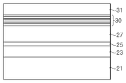
도 1은 종래 기술에 따른 자외선 발광 다이오드 제조 방법을 설명하기 위한 개략적인 단면도이고, 도 2는 도 1의 활성 영역을 확대 도시한 단면도이다.1 is a schematic cross-sectional view for explaining a method of manufacturing an ultraviolet light emitting diode according to the prior art, and FIG. 2 is an enlarged cross-sectional view of the active region of FIG. 1.
도 1 및 도 2를 참조하면, 기판(21) 상에 버퍼층(23), AlN층(25), n형 AlGaN층(27), 다중 양자우물 구조의 활성 영역(30) 및 p형 AlGaN층(31)이 형성된다.1 and 2, the
기판(21)은 사파이어 기판이고, 버퍼층(23)은 레이저 리프트 오프 공정을 위한 희생 버퍼층으로서 일반적으로 GaN로 형성된다. 버퍼층(23)은, 잘 알려진 바와 같이, 핵층 및 고온 버퍼층을 포함할 수 있다.The
이 분야에서 잘 알려진 바와 같이, p형 AlGaN층(31) 상에 지지기판이 부착되고, 레이저 리프트 오프 공정을 통해 기판(21)이 제거된다. 나아가, 버퍼층(23) 및 AlN층(25) 또한 제거되고 n형 AlGaN층(27)의 표면이 노출될 것이다.As is well known in the art, a supporting substrate is attached on the p-
한편, 활성 영역(30)은 장벽층(30b) 및 웰층(30w)이 교대로 적층된 다중 양자우물 구조를 가진다. 활성 영역(30)의 첫째층 및 마지막층은 장벽층(30b) 또는 웰층(30w)일 수 있다.Meanwhile, the
종래 기술에 따르면, 장벽층(30b) 및 웰층(30w)은 Al을 함유하는 질화물계 반도체층, 예컨대 AlGaN 또는 AlInGaN으로 형성된다. AlGaN이나 AlInGaN을 적층한 경우, 각 층들 내에 잔류하는 응력에 의해 밴드 벤딩 현상이 InGaN/GaN에 비해 상당히 크게 나타난다. 이에 따라, 자외선 발광 다이오드의 내부양자효율이 감소하고 또한 전류 증가에 따라 방출되는 광의 파장이 크게 변한다. 더욱이, 두께를 정밀하게 제어하지 못할 경우, 활성 영역(30) 상에 형성되는 층, 예컨대 p형 AlGaN층(31)에 크랙이 유발될 수 있으며, 따라서 발광 다이오드의 불량을 초래한다.According to the prior art, the
한편, 상기 종래 기술은 장벽층 및 웰층을 AlGaN 또는 AlInGaN으로 형성한다. 장벽층이나 웰층은 일반적으로 나노 스케일의 매우 얇은 두께를 갖는다. 이와 같이, 얇은 두께를 가지는 층을 AlGaN 또는 AlInGaN으로 형성할 경우, 성장되는 층의 조성은 그 아래 층의 조성에 강한 의존성을 나타낸다. 즉, 동일한 성장 조건으로 AlGaN층을 성장하더라도, 그 아래 층의 질화물계 반도체층의 조성이 바뀌면, 다른 조성을 가지는 AlGaN층이 성장한다.Meanwhile, in the prior art, the barrier layer and the well layer are formed of AlGaN or AlInGaN. The barrier layer or well layer generally has a very thin thickness of nanoscale. As described above, when a layer having a thin thickness is formed of AlGaN or AlInGaN, the composition of the grown layer exhibits a strong dependence on the composition of the underlying layer. That is, even if the AlGaN layer is grown under the same growth conditions, when the composition of the nitride-based semiconductor layer under the layer is changed, the AlGaN layer having a different composition is grown.
이에 따라, 런-투-런(run-to-run), 웨이퍼-투-웨이퍼(wafer-to-wafer)로 전기적 및 광학적 특성이 균일한 발광 다이오드들을 제조하기 어려우며, 나아가, 동일 웨이퍼 내에서 제조된 발광 다이오드들 또한 전기적 및 광학적 특성의 편차가 심하다.Accordingly, it is difficult to manufacture light-emitting diodes having uniform electrical and optical characteristics with a run-to-run, wafer-to-wafer, and further, it is manufactured in the same wafer. Light-emitting diodes also have a large variation in electrical and optical properties.
본 발명이 해결하고자 하는 과제는, 크랙과 같은 결정 결함의 발생을 방지할 수 있는 질화갈륨계 자외선 발광 다이오드 및 그 제조 방법을 제공하는 것이다.The problem to be solved by the present invention is to provide a gallium nitride-based ultraviolet light emitting diode and a method of manufacturing the same, which can prevent the occurrence of crystal defects such as cracks.
본 발명이 해결하고자 하는 또 다른 과제는, 웰층 및/또는 장벽층의 조성을 균일하게 제어할 수 있는 발광 다이오드 및 그 제조 방법을 제공하는 것이다.Another problem to be solved by the present invention is to provide a light emitting diode and a method for manufacturing the same, which can uniformly control the composition of the well layer and / or barrier layer.
본 발명이 해결하고자 하는 또 다른 과제는, 균일한 전기적 및 광학적 특성을 갖는 자외선 발광 다이오드 제조 방법을 제공하는 것이다.Another problem to be solved by the present invention is to provide a method for manufacturing an ultraviolet light emitting diode having uniform electrical and optical properties.
본 발명의 일 실시예에 따른 자외선 발광 다이오드는, n형 질화물계 반도체층과 p형 질화물계 반도체층 사이에 활성 영역을 포함하며, 상기 활성 영역은, Al을 함유하는 복수의 장벽층들; 상기 장벽층들과 교대로 정렬되고, Al을 함유하는 복수의 웰층들; 및 적어도 하나의 컨디셔닝층을 포함한다. 각각의 컨디셔닝층은 웰층과 그것에 이웃하는 장벽층 사이에 위치하며, 2성분계 질화물 반도체로 형성된다.An ultraviolet light emitting diode according to an embodiment of the present invention includes an active region between an n-type nitride-based semiconductor layer and a p-type nitride-based semiconductor layer, the active region comprising: a plurality of barrier layers containing Al; A plurality of well layers alternately aligned with the barrier layers and containing Al; And at least one conditioning layer. Each conditioning layer is located between the well layer and the barrier layer adjacent to it, and is formed of a two-component nitride semiconductor.
상기 컨디셔닝층을 채택함으로써, 활성 영역의 응력을 감소시킬 수 있으며, 또한, 웰층 및/또는 장벽층의 조성을 균일하게 제어할 수 있다.By adopting the conditioning layer, stress in the active region can be reduced, and the composition of the well layer and / or barrier layer can be uniformly controlled.
상기 2성분계 질화물 반도체는 GaN 또는 AlN일 수 있다. 특히, AlN는 웰층의 밴드갭보다 넓은 밴드갭을 가지므로, 웰층에서 생성된 광을 흡수하지 않으며, 따라서, 광 손실을 줄일 수 있다.The bi-component nitride semiconductor may be GaN or AlN. In particular, since AlN has a band gap wider than that of the well layer, it does not absorb light generated in the well layer, and thus, light loss can be reduced.
일 실시예에 있어서, 상기 적어도 하나의 컨디셔닝층은 상기 n형 질화물계 반도체층 측에서 웰층에 접하는 웰-컨디셔닝층을 포함할 수 있다.In one embodiment, the at least one conditioning layer may include a well-conditioning layer contacting the well layer on the n-type nitride-based semiconductor layer side.
다른 실시예에 있어서, 상기 적어도 하나의 컨디셔닝층은 상기 n형 질화물계 반도체층 측에서 장벽층에 접하는 장벽-컨디셔닝층을 포함할 수 있다.In another embodiment, the at least one conditioning layer may include a barrier-conditioning layer contacting the barrier layer on the n-type nitride-based semiconductor layer side.
상기 적어도 하나의 컨디셔닝층은 상기 웰-컨디셔닝층 및 장벽-컨디셔닝층 모두를 포함할 수 있다.The at least one conditioning layer may include both the well-conditioning layer and the barrier-conditioning layer.
한편, 상기 장벽층들은 일정한 조성을 가질 수 있으나, 이에 한정되는 것은 아니며, 조성 경사층일 수도 있다. 일 실시예에서, 상기 웰-컨디셔닝층에 인접한 장벽층은 상기 웰-컨디셔닝층을 향해 Al의 함량이 증가하는 조성 경사층일 수 있다.Meanwhile, the barrier layers may have a certain composition, but are not limited thereto, and may be a composition gradient layer. In one embodiment, the barrier layer adjacent to the well-conditioning layer may be a composition gradient layer in which the content of Al increases toward the well-conditioning layer.
상기 복수의 장벽층들 및 웰층들은 AlInGaN 또는 AlGaN으로 형성될 수 있다. 나아가, 상기 n형 질화물계 반도체층 및 p형 질화물계 반도체층은 AlInGaN 또는 AlGaN층을 포함할 수 있다.The plurality of barrier layers and the well layers may be formed of AlInGaN or AlGaN. Furthermore, the n-type nitride-based semiconductor layer and the p-type nitride-based semiconductor layer may include an AlInGaN or AlGaN layer.
본 발명의 다른 실시예에 따른 자외선 발광 다이오드는, n형 질화물계 반도체층과 p형 질화물계 반도체층 사이에 활성 영역을 포함하며, 상기 활성 영역은, Al을 함유하는 복수의 장벽층들; 및 상기 장벽층들과 교대로 정렬되고, Al을 함유하는 복수의 웰층들을 포함하고, 상기 복수의 장벽층들 중 적어도 하나는 웰층과 웰층 사이에서 Al의 함량이 증가하는 조성 경사층을 포함한다. 나아가, 상기 p형 질화물계 반도체층측의 상기 조성 경사층의 끝단의 조성은 AlN이다.An ultraviolet light emitting diode according to another embodiment of the present invention includes an active region between an n-type nitride-based semiconductor layer and a p-type nitride-based semiconductor layer, the active region comprising: a plurality of barrier layers containing Al; And a plurality of well layers alternately aligned with the barrier layers and containing Al, and at least one of the plurality of barrier layers includes a composition gradient layer in which the content of Al increases between the well layer and the well layers. Further, the composition of the end of the composition gradient layer on the p-type nitride-based semiconductor layer side is AlN.
조성 경사층의 끝단의 조성을 AlN가 되도록 함으로써, 그 위의 웰층의 조성이 용이하게 제어될 수 있다.Composition By making the composition at the end of the gradient layer AlN, the composition of the well layer thereon can be easily controlled.
나아가, 상기 자외선 발광 다이오드는, 상기 활성영역과 상기 n형 질화물계 반도체층 사이에서 상기 활성 영역에 접하는 2성분계 질화물 반도체의 컨디셔닝층을 더 포함할 수 있다. 상기 활성 영역에 접하는 컨디셔닝층은 GaN 또는 AlN로 형성될 수 있다.Furthermore, the ultraviolet light emitting diode may further include a conditioning layer of a two-component nitride semiconductor contacting the active region between the active region and the n-type nitride-based semiconductor layer. The conditioning layer contacting the active region may be formed of GaN or AlN.
한편, 상기 복수의 웰층들은 AlInGaN 또는 AlGaN으로 형성될 수 있다. 나아가, 상기 복수의 장벽층들은 AlInGaN 또는 AlGaN을 포함할 수 있다.Meanwhile, the plurality of well layers may be formed of AlInGaN or AlGaN. Furthermore, the plurality of barrier layers may include AlInGaN or AlGaN.
본 발명의 또 다른 실시예에 따른 자외선 발광 다이오드 제조 방법은, n형 질화물계 반도체층과 p형 질화물계 반도체층 사이에 활성 영역을 포함하는 자외선 발광 다이오드 제조 방법에 있어서, 기판 상에 n형 질화물계 반도체층을 성장시키고, 상기 n형 질화물계 반도체층 상에 Al을 함유하는 복수의 장벽층들과 Al을 함유하는 복수의 웰층들을 교대로 성장시켜 활성 영역을 형성하고, 상기 활성 영역 상에 p형 질화물계 반도체층을 성장시키는 것을 포함한다. 나아가, 상기 활성 영역을 형성하는 것은, 적어도 하나의 웰층 또는 적어도 하나의 장벽층을 성장시키기 전에, 컨디셔닝층을 성장시키는 것을 포함하고, 상기 컨디셔닝층은 2성분계 질화물 반도체로 형성된다.A method of manufacturing an ultraviolet light emitting diode according to another embodiment of the present invention, In the method of manufacturing an ultraviolet light emitting diode comprising an active region between the n-type nitride-based semiconductor layer and the p-type nitride-based semiconductor layer, n-type nitride on the substrate An active region is formed by alternately growing a plurality of barrier layers containing Al and a plurality of well layers containing Al on the n-type nitride-based semiconductor layer, and p on the active region. And growing the nitride semiconductor layer. Further, forming the active region includes growing a conditioning layer before growing at least one well layer or at least one barrier layer, and the conditioning layer is formed of a two-component nitride semiconductor.
웰층 또는 장벽층을 성장시키기 전에, 2성분계 질화물 반도체의 컨디셔닝층을 먼저 성장시킴으로써, 그 위에 성장되는 웰층 또는 장벽층의 조성을 용이하게 제어할 수 있다.Before growing the well layer or barrier layer, by first growing the conditioning layer of the two-component nitride semiconductor, the composition of the well layer or barrier layer grown thereon can be easily controlled.
상기 컨디셔닝층은 GaN 또는 AlN로 형성될 수 있다. 특히, AlN는 웰층의 밴드갭보다 넓은 밴드갭을 가지므로, 웰층에서 생성된 광을 흡수하지 않으며, 따라서, 광 손실을 줄일 수 있다.The conditioning layer may be formed of GaN or AlN. In particular, since AlN has a band gap wider than that of the well layer, it does not absorb light generated in the well layer, and thus, light loss can be reduced.
상기 활성 영역을 형성하는 것은, 복수의 웰층들 및 복수의 장벽층들 각각을 성장시키기 전에, 컨디셔닝층을 성장시키는 것을 포함할 수 있다.Forming the active region may include growing a conditioning layer before growing each of the plurality of well layers and the plurality of barrier layers.
한편, 상기 복수의 장벽층들 및 복수의 웰층들은 AlInGaN 또는 AlGaN으로 형성될 수 있다.Meanwhile, the plurality of barrier layers and the plurality of well layers may be formed of AlInGaN or AlGaN.
본 발명의 또 다른 실시예에 따른 자외선 발광 다이오드 제조 방법은, n형 질화물계 반도체층과 p형 질화물계 반도체층 사이에 활성 영역을 포함하는 자외선 발광 다이오드 제조 방법에 있어서, 기판 상에 n형 질화물계 반도체층을 성장시키고, 상기 n형 질화물계 반도체층 상에 Al을 함유하는 복수의 장벽층들과 Al을 함유하는 복수의 웰층들을 교대로 성장시켜 활성 영역을 형성하고, 상기 활성 영역 상에 p형 질화물계 반도체층을 성장시키는 것을 포함한다. 나아가, 상기 복수의 장벽층들 중 웰층들 사이에 위치하는 적어도 하나의 장벽층은 웰층 상에서 Al의 함량이 증가하는 조성 경사층으로 형성되고, 상기 조성 경사층의 끝단의 조성은 AlN이다.A method of manufacturing an ultraviolet light emitting diode according to another embodiment of the present invention, In the method of manufacturing an ultraviolet light emitting diode comprising an active region between the n-type nitride-based semiconductor layer and the p-type nitride-based semiconductor layer, n-type nitride on the substrate An active region is formed by alternately growing a plurality of barrier layers containing Al and a plurality of well layers containing Al on the n-type nitride-based semiconductor layer, and p on the active region. And growing the nitride semiconductor layer. Furthermore, at least one barrier layer positioned between well layers among the plurality of barrier layers is formed of a composition gradient layer in which the content of Al increases on the well layer, and the composition of the end of the composition gradient layer is AlN.
조성 경사층의 끝단의 조성이 AlN이므로, 그 위에 성장되는 웰층의 조성을 용이하게 제어할 수 있다.Composition Since the composition of the tip of the gradient layer is AlN, the composition of the well layer grown thereon can be easily controlled.
상기 복수의 장벽층들 및 복수의 웰층들은 AlInGaN 또는 AlGaN으로 형성될 수 있다.The plurality of barrier layers and the plurality of well layers may be formed of AlInGaN or AlGaN.
나아가, 상기 자외선 발광 다이오드 제조 방법은, 상기 활성 영역을 형성하기 전에 2성분계 질화물 반도체의 컨디셔닝층을 형성하는 것을 더 포함할 수 있다. 상기 2성분계 질화물 반도체는 GaN 또는 AlN일 수 있다.Furthermore, the method of manufacturing the ultraviolet light emitting diode may further include forming a conditioning layer of a two-component nitride semiconductor before forming the active region. The bi-component nitride semiconductor may be GaN or AlN.
본 발명의 실시예들에 따르면, 웰층 또는 장벽층을 성장시키기 전에 컨디셔닝층을 먼저 성장함으로써 웰층 또는 장벽층의 조성을 용이하게 제어할 수 있다. 나아가, 웰층 및 장벽층의 조성을 균일하게 제어함으로써, 크랙과 같은 결정 결함의 발생을 방지할 수 있는 질화갈륨계 자외선 발광 다이오드를 제공할 수 있다.According to embodiments of the present invention, the composition of the well layer or barrier layer can be easily controlled by first growing the conditioning layer before growing the well layer or barrier layer. Furthermore, by uniformly controlling the composition of the well layer and the barrier layer, it is possible to provide a gallium nitride-based ultraviolet light emitting diode capable of preventing the occurrence of crystal defects such as cracks.
도 1은 종래 기술에 따른 자외선 발광 다이오드 제조 방법을 설명하기 위한 개략적인 단면도이다.
도 2는 도 1의 활성 영역 부분을 확대 도시한 단면도이다.
도 3은 본 발명의 일 실시예에 따른 자외선 발광 다이오드를 설명하기 위해 활성 영역 부분을 확대 도시한 단면도이다.
도 4는 본 발명의 또 다른 실시예에 따른 자외선 발광 다이오드를 설명하기 위해 활성 영역 부분을 확대 도시한 단면도이다.
도 5(a) 및 도 5(b)는 각각 도 3 및 도 4의 실시예들에 따라 제조된 샘플들의 단면 TEM 사진들이다.
도 6(a) 및 도 6(b)는 각각 컨디셔닝층 또는 조성 경사층 채택에 따른 테스트 샘플들의 평면 광학 사진들이다.
도 7(a) 및 도 7(b)는 각각 종래 기술에 따라 형성된 테스트 샘플의 평면 사진들이다.
도 8은 종래 기술에 따라 함께 제조된 웨이퍼 그룹과 본 발명의 일 실시예에 따라 제조된 웨이퍼 그룹의 PL(photo-luminescence) 파장 분포를 나타내는 그래프이다.
도 9는 종래 기술에 따라 제조된 웨이퍼 및 본 발명의 일 실시예에 따라 제조된 웨이퍼의 PL 강도를 나타내는 그래프이다.1 is a schematic cross-sectional view for explaining a method of manufacturing an ultraviolet light emitting diode according to the prior art.
FIG. 2 is an enlarged cross-sectional view of an active region portion of FIG. 1.
3 is an enlarged cross-sectional view of an active region portion to describe an ultraviolet light emitting diode according to an embodiment of the present invention.
4 is an enlarged cross-sectional view of an active region portion for explaining an ultraviolet light emitting diode according to another embodiment of the present invention.
5 (a) and 5 (b) are cross-sectional TEM photographs of samples prepared according to the embodiments of FIGS. 3 and 4, respectively.
6 (a) and 6 (b) are planar optical photographs of test samples according to the adoption of a conditioning layer or a composition gradient layer, respectively.
7 (a) and 7 (b) are plan views of a test sample formed according to the prior art, respectively.
FIG. 8 is a graph showing a wavelength distribution of PL (photo-luminescence) of a wafer group manufactured according to the prior art and a wafer group manufactured according to an embodiment of the present invention.
9 is a graph showing PL strength of a wafer manufactured according to the prior art and a wafer manufactured according to an embodiment of the present invention.
이하, 첨부한 도면들을 참조하여 본 발명의 실시예들을 상세히 설명한다. 다음에 소개되는 실시예들은 당업자에게 본 발명의 사상이 충분히 전달될 수 있도록 하기 위해 예로서 제공되는 것이다. 따라서, 본 발명은 이하 설명되는 실시예에 한정되지 않고 다른 형태로 구체화될 수 있다. 그리고, 도면에 있어서, 구성요소의 폭, 길이, 두께 등은 편의를 위하여 과장되어 표현될 수 있다. 명세서 전체에 걸쳐서 동일한 참조번호들은 동일한 구성요소들을 나타낸다.Hereinafter, embodiments of the present invention will be described in detail with reference to the accompanying drawings. The following embodiments are provided as examples to ensure that the spirit of the present invention is sufficiently conveyed to those skilled in the art. Therefore, the present invention is not limited to the embodiments described below and may be embodied in other forms. In addition, in the drawings, the width, length, and thickness of components may be exaggerated for convenience. Throughout the specification, the same reference numbers refer to the same components.
도 3은 본 발명의 일 실시예에 따른 자외선 발광 다이오드를 설명하기 위해 활성 영역 부분을 확대 도시한 단면도이다.3 is an enlarged cross-sectional view of an active region portion to describe an ultraviolet light emitting diode according to an embodiment of the present invention.
도 3을 참조하면, 상기 자외선 발광 다이오드는 n형 질화물계 반도체층(27)과 p형 질화물계 반도체층(31) 사이에 활성 영역(50)을 가진다. 상기 자외선 발광 다이오드는 또한 도 1에 도시한 것과 같은 성장 기판(21) 또는 지지기판을 포함할 수 있다.Referring to FIG. 3, the ultraviolet light emitting diode has an
n형 질화물계 반도체층(27) 및 p형 질화물계 반도체층(27)은 활성층(30w)보다 넓은 밴드갭을 갖는 질화물계 반도체층으로 형성된다. n형 질화물계 반도체층(27) 및 p형 질화물계 반도체층(31)은 각각 Al을 함유하는 층, 예컨대 AlInGaN층 또는 AlGaN층을 포함할 수 있다.The n-type nitride-based
활성 영역(50)은 복수의 장벽층들(30b), 복수의 웰층들(30w) 및 컨디셔닝층들(30cb, 30cw)을 포함한다. 한편, 컨디셔닝층들(30cb, 30cw)은 웰-컨디셔닝층(30cw) 및 장벽-컨디셔닝층(30cb)를 포함한다.The
장벽층들(30b)과 웰층들(30w)은 서로 교대로 정렬되어 다중 양자우물 구조를 형성한다. 웰층들(30w)은 요구되는 자외선 파장, 예컨대 200 내지 365nm 범위 내의 자외선을 방출하는 질화물계 반도체층으로 형성된다. 일 실시예에서, 웰층들(30w)은 250 내지 340nm 범위 내의 자외선을 방출하는 질화물계 반도체층으로 형성될 수 있다. 웰층들(30w)은 Al을 함유하며, AlInGaN 또는 AlGaN으로 형성될 수 있다.The barrier layers 30b and the well layers 30w are alternately aligned with each other to form a multiple quantum well structure. The well layers 30w are formed of a nitride-based semiconductor layer that emits ultraviolet rays within a required ultraviolet wavelength range, for example, 200 to 365 nm. In one embodiment, the well layers 30w may be formed of a nitride-based semiconductor layer that emits ultraviolet rays in the range of 250 to 340 nm. The well layers 30w contain Al, and may be formed of AlInGaN or AlGaN.
장벽층들(30b)은 웰층들(30w)보다 넓은 밴드갭을 가지는 질화물계 반도체층으로 형성된다. 장벽층들(30b)은 Al을 함유하며, AlInGaN 또는 AlGaN으로 형성될 수 있다. 장벽층들(30b) 각각은 일정한 조성을 갖도록 형성될 수 있으나, 이에 한정되는 것은 아니다. 적어도 하나의 장벽층(30b)은 조성이 다른 층들의 적층 구조로 형성될 수 있으며, 조성 경사층으로 형성될 수 있다. 특히, 웰층(30w)들 사이에 위치하는 장벽층(30b)이 조성 경사층으로 형성될 수 있다.The barrier layers 30b are formed of a nitride-based semiconductor layer having a wider band gap than the
컨디셔닝층들(30cb, 30cw)은 각각 웰층(30w)과 그것에 이웃하는 장벽층(30b) 사이에 위치한다. 웰 컨디셔닝층(30cw)은 n형 질화물계 반도체층(27) 측에서 웰층(30w)에 접한다. 한편, 장벽 컨디셔닝층(30cb)은 n형 질화물계 반도체층(27) 측에서 장벽층(30b)에 접한다.The conditioning layers 30cb and 30cw are located between the
컨디셔닝층들(30cb, 30cw)은 2성분계 질화물계 반도체층, 예컨대, GaN 또는 AlN로 형성될 수 있다. 컨디셔닝층들(30cb, 30cw)은, 2성분계 질화물계 반도체층이므로, 3성분계 또는 4성분계 질화물계 반도체층에 비해 균일한 조성을 갖는다. 일 실시예에서, 컨디셔닝층들(30cb, 30cw)은 AlN로 형성될 수 있다. AlN는 웰층(30w)보다 넓은 밴드갭을 가지므로, 광을 흡수하지 않으며, 따라서, 광 손실을 줄일 수 있다.The conditioning layers 30cb and 30cw may be formed of a two-component nitride-based semiconductor layer, for example, GaN or AlN. Since the conditioning layers 30cb and 30cw are two-component nitride-based semiconductor layers, they have a uniform composition compared to three- or four-component nitride-based semiconductor layers. In one embodiment, the conditioning layers 30cb, 30cw may be formed of AlN. Since AlN has a wider band gap than the
본 실시예에 있어서, 상기 자외선 발광 다이오드는 수직 구조일 수 있으나, 이에 한정되는 것은 아니며, 수평 구조일 수도 있다. 수직 구조의 경우, 상기 자외선 발광 다이오드는 질화물계 반도체층들(27, 50, 31)을 지지하기 위한 지지 기판을 포함할 것이다. 이와 달리, 수평 구조의 경우, 상기 자외선 발광 다이오드는 질화물계 반도체층들(27, 50, 31)을 성장시키기 위한 성장 기판을 포함할 것이다.In the present embodiment, the ultraviolet light emitting diode may have a vertical structure, but is not limited thereto, and may also have a horizontal structure. In the case of a vertical structure, the ultraviolet light emitting diode will include a support substrate for supporting the nitride-based semiconductor layers 27, 50 and 31. Alternatively, in the case of a horizontal structure, the ultraviolet light emitting diode will include a growth substrate for growing the nitride-based semiconductor layers 27, 50, and 31.
한편, 본 실시예에 있어서, 웰-컨디셔닝층들(30cw)이 모든 웰층들(30c)에 접하여 형성된 것으로 도시 및 설명하지만, 본 발명은 이에 한정되는 것은 아니다. 즉, 일부 웰층들(30c) 또는 하나의 웰층(30c)에 접하여 웰-컨디셔닝층(들)(30cw)이 형성될 수 있다. 또한, 장벽-컨디셔닝층들(30cb)이 모든 장벽층들(30b)에 접하여 형성된 것으로 도시 및 설명하지만, 본 발명은 이에 한정되는 것은 아니다. 즉, 일부 장벽층들(30b) 또는 하나의 장벽층(30b)에 접하여 장벽-컨디셔닝층(들)(30cb)이 형성될 수 있다.On the other hand, in the present embodiment, the well-conditioning layers 30cw are illustrated and described as being formed in contact with all well layers 30c, but the present invention is not limited thereto. That is, the well-conditioning layer (s) 30cw may be formed in contact with some well layers 30c or one well layer 30c. In addition, although the barrier-conditioning layers 30cb are illustrated and described as being formed in contact with all the barrier layers 30b, the present invention is not limited thereto. That is, the barrier-conditioning layer (s) 30cb may be formed in contact with some barrier layers 30b or one
이하, 앞의 실시예의 자외선 발광 다이오드 제조 방법을 설명한다.Hereinafter, a method of manufacturing the ultraviolet light emitting diode of the previous embodiment will be described.
우선, 도 1에 도시한 바와 같은 기판(21) 상에 n형 질화물계 반도체층(27)이 성장된다. n형 질화물계 반도체층(27)을 성장하기 전, 종래기술에서 설명한 바와 같은 층들, 예컨대 버퍼층(23) 및 AlN층(25) 등이 성장될 수 있다. n형 질화물계 반도체층(27)을 형성하기 전에 기판(21) 상에 형성되는 층들은 다양하게 변형될 수 있으며, 공지의 다양한 층들이 용도에 맞게 선택될 수 있다.First, an n-type nitride-based
n형 질화물계 반도체층(27)은 금속 유기화학 기상 성장법(MOCVD)을 이용하여 성장될 수 있다. n형 질화물계 반도체층(27)은 단일층 또는 다중층으로 형성될 수 있으며, AlInGaN층 또는 AlGaN층을 포함한다.The n-type nitride-based
상기 n형 질화물계 반도체층(27) 상에 활성 영역(50)이 성장된다. 활성 영역(50)은 Al을 함유하는 복수의 장벽층들(30b)과 Al을 함유하는 복수의 웰층들(30w)을 교대로 성장시켜 형성된다. 다만, 장벽층들(30b)을 성장하기 전에 장벽 컨디셔닝층(30cb)이 먼저 성장되고, 웰층들(30w)을 성장하지 전에 웰-컨디셔닝층(30cw)이 먼저 성장된다. 상기 컨디셔닝층들(30cb, 30cw)은 2성분계 질화물 반도체, 예컨대 GaN 또는 AlN로 형성된다.The
이에 따라, 장벽층들(30b) 하부의 층들, 예컨대, n형 질화물계 반도체층(27) 또는 웰층들(30w)의 조성이 변하더라도, 장벽층들(30b)은 모두 균일한 조성의 장벽-컨디셔닝층(30cb) 상에서 성장될 수 있다. 따라서, 장벽층들(30b)의 조성이 용이하게 제어될 수 있다.Accordingly, even if the composition of the layers under the barrier layers 30b, for example, the n-type nitride-based
또한, 웰층들(30w)의 하부의 층들, 예컨대, 장벽층들(30b)의 조성이 변하더라도, 웰층들(30w)은 모두 균일한 조성의 웰-컨디셔닝층(30cw) 상에서 성장될 수 있다. 따라서, 웰층들(30w)의 조성이 용이하게 제어될 수 있다.In addition, even if the composition of the lower layers of the
이어서, 활성 영역(50) 상에 p형 질화물계 반도체층(31)이 성장된다. p형 질화물계 반도체층(31)은 단일층 또는 다중층으로 형성될 수 있으며, AlInGaN층 또는 AlGaN층을 포함할 수 있다.Subsequently, a p-type nitride-based
상기 자외선 발광 다이오드는 수평 구조 또는 수직 구조의 발광 다이오드로 제조될 수 있으며, 이에 대한 자세한 설명은 생략한다.The ultraviolet light emitting diode may be made of a light emitting diode having a horizontal structure or a vertical structure, and detailed description thereof will be omitted.
본 실시예에 따르면, 웰-컨디셔닝층(30cw) 및/또는 장벽-컨디셔닝층(30cb)을 채택함으로써, 웰층들(30w) 및/또는 장벽층들(30b)의 조성을 용이하게 제어할 수 있다. 따라서, 활성 영역(50) 내의 잔류 응력을 감소시킬 수 있어, 활성 영역(50) 상에 성장되는 p형 질화물계 반도체층(31)에 크랙 등의 결함이 발생하는 것을 방지할 수 있다. 나아가, 웰층들(30w) 및/또는 장벽층들(30b)의 조성을 균일하게 제어할 수 있다. 따라서, 동일 웨이퍼 내에서 제조된 발광 다이오드들의 전기적 및 광학적 특성이 균일할 뿐만 아니라, 런-투-런, 웨이퍼-투-웨이퍼로 제조된 발광 다이오드들 또한 균일한 전기적 및 광학적 특성을 가질 수 있다.According to this embodiment, by adopting the well-conditioning layer 30cw and / or barrier-conditioning layer 30cb, it is possible to easily control the composition of the well layers 30w and / or
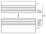
도 4는 본 발명의 또 다른 실시예에 따른 자외선 발광 다이오드를 설명하기 위해 활성 영역 부분을 확대 도시한 단면도이다.4 is an enlarged cross-sectional view of an active region portion for explaining an ultraviolet light emitting diode according to another embodiment of the present invention.
도 4를 참조하면, 상기 자외선 발광 다이오드는 n형 질화물계 반도체층(27)과 p형 질화물계 반도체층(31) 사이에 활성 영역(60)을 가진다. 상기 자외선 발광 다이오드는 또한 도 1에 도시한 것과 같은 성장 기판(21) 또는 지지기판을 포함할 수 있다.Referring to FIG. 4, the ultraviolet light emitting diode has an
n형 질화물계 반도체층(27), p형 질화물계 반도체층(27), 성장 기판(21), 및 지지기판은 도 3을 참조하여 설명한 바와 동일하므로, 중복을 피하기 위해 상세한 설명은 생략한다.Since the n-type nitride-based
활성 영역(50)은 복수의 장벽층들(30b, 30gb) 및 복수의 웰층들(30w)을 포함한다.The
장벽층들(30gb)과 웰층들(30w)은 서로 교대로 정렬되어 다중 양자우물 구조를 형성한다. 웰층들(30w)은 도 3을 참조하여 설명한 바와 중복되므로, 상세한 설명은 생략한다. 한편, 장벽층들(30gb)는 웰층들(30w)보다 넓은 밴드갭을 가지는 질화물계 반도체층으로 형성된다. 장벽층들(30gb)은 Al을 함유하며, AlInGaN 또는 AlGaN을 포함할 수 있다.The barrier layers 30gb and the well layers 30w are alternately aligned with each other to form a multiple quantum well structure. Since the well layers 30w are overlapped with those described with reference to FIG. 3, detailed description is omitted. Meanwhile, the barrier layers 30gb are formed of a nitride-based semiconductor layer having a wider band gap than the
장벽층들(30gb)은 특히 웰층(30w)들 사이에 위치하며, Al 함량이 증가하는 조성 경사층이다. p형 질화물계 반도체층(31) 측의 상기 조성 경사층(30gb)의 끝단의 조성은 AlN이다. 조성 경사층(30gb)의 끝단의 조성을 AlN로 함으로써, 그 위에 성장되는 웰층(30w)의 조성을 용이하게 제어할 수 있다.The barrier layers 30gb are particularly located between the well layers 30w and are composition gradient layers in which the Al content is increased. The composition of the end of the composition gradient layer 30gb on the p-type nitride-based
일 실시예에 있어서, 활성 영역(60)은 n형 질화물계 반도체층(27)에 인접하여 위치하는 장벽층(30b)을 더 포함할 수 있다. 장벽층(30b)은 도 3을 참조하여 설명한 장벽층(30b)과 동일하며, 예컨대 일정한 조성층일 수 있다. 이 경우, 장벽-컨디셔닝층(30cb)이 n형 질화물계 반도체층(27) 측에서 장벽층(30b)에 접할 수 있다. 또한, 도시하지는 않았지만, 장벽층(30b)과 그 위에 위치하는 웰층(30w) 사이에 도 3을 참조하여 설명한 바와 같은 웰-컨디셔닝층(30cw)이 위치할 수 있다.In one embodiment, the
다른 실시예에 있어서, 웰층(30w)이 n형 질화물계 반도체층(27)에 인접하여 위치할 수 있으며, 이 경우, 웰-컨디셔닝층(도 3의 30cw)이 n형 질화물계 반도체층(27) 측에서 웰층(30w)에 접할 수 있다.In another embodiment, the
본 실시예에 있어서, 상기 자외선 발광 다이오드는, 도 3을 참조하여 설명한 바와 같이, 수직 구조 또는 수평 구조일 수 있다.In the present embodiment, the ultraviolet light emitting diode may have a vertical structure or a horizontal structure, as described with reference to FIG. 3.
한편, 본 실시예에 있어서, n형 질화물계 반도체층(27)에 인접한 장벽층(30b)을 제외하고 모든 장벽층들(30gb)이 조성 경사층인 것으로 도시 및 설명하지만, 본 발명은 이에 한정되는 것은 아니다. 즉, 일부 장벽층들 또는 하나의 장벽층만이 조성 경사층이고, 나머지 장벽층들은 일정한 조성을 가질 수 있다. 또한, 상기 활성 영역(60)은 조성이 다른 층들의 적층 구조를 갖는 장벽층을 포함할 수도 있다. 나아가, 상기 활성 영역(60)은 조성 경사층의 장벽층(30gb)과 함께, 컨디셔닝층(30cw 또는 30cb)들을 그 내부에 포함할 수 있다.On the other hand, in the present embodiment, all barrier layers 30gb except for the
이하, 앞의 실시예의 자외선 발광 다이오드 제조 방법을 설명한다.Hereinafter, a method of manufacturing the ultraviolet light emitting diode of the previous embodiment will be described.
본 실시예에 따른 자외선 발광 다이오드 제조 방법은 활성 영역(60)을 제외하면, 도 3을 참조하여 설명한 제조 방법과 유사하므로, 중복을 피하기 위해, 그 차이점에 대해서만 상세히 설명한다.The manufacturing method of the ultraviolet light emitting diode according to this embodiment is similar to the manufacturing method described with reference to FIG. 3 except for the
기판(21) 상에 n형 질화물계 반도체층(27)이 성장된 후, n형 질화물계 반도체층(27) 상에 활성 영역(60)이 성장된다. 활성 영역(60)은 Al을 함유하는 복수의 장벽층들(30b, 30gb)과 Al을 함유하는 복수의 웰층들(30w)을 교대로 성장시켜 형성된다. 장벽층(30b)은 생략될 수도 있다. 복수의 웰층들(30w)은 AlInGaN층 또는 AlGaN층으로 형성될 수 있다. After the n-type nitride-based
또한, 장벽층들(30b, 30gb)은 AlInGaN 또는 AlGaN으로 형성될 수 있다. 다만, 장벽층들(30b, 30gb) 중 웰층들(30w) 사이에 위치하는 장벽층들(30gb)은 웰층(30w) 상에서 Al의 함량이 증가하는 조성 경사층으로 형성되며, 조성 경사층(30w)의 끝단의 조성은 AlN이다. 예컨대, 장벽층(30gb)은 웰층(30w)의 조성으로부터 Al의 함량이 증가하고, Ga 또는 In의 함량이 감소하여 AlN의 조성으로 성장이 종료될 수 있다. 조성 경사층(30gb)을 채택함으로써, 활성 영역(60) 내의 잔류 응력을 줄일 수 있다. 나아가, 조성 경사층의 끝단의 조성을 AlN로 설정함으로써, 장벽층(30gb) 상에 성장되는 웰층(30w)의 조성을 용이하게 제어할 수 있다.In addition, the barrier layers 30b and 30gb may be formed of AlInGaN or AlGaN. However, of the barrier layers 30b and 30gb, the barrier layers 30gb positioned between the well layers 30w are formed of a composition gradient layer in which the content of Al increases on the
본 실시예에 따르면, 조성 경사층의 장벽층(30gb)을 채택함으로써, 웰층(30w)의 조성을 균일하게 제어할 수 있다. 따라서, 동일 웨이퍼 내에서 제조된 발광 다이오드들의 전기적 및 광학적 특성이 균일할 뿐만 아니라, 런-투-런, 웨이퍼-투-웨이퍼로 제조된 발광 다이오드들 또한 균일한 전기적 및 광학적 특성을 가질 수 있다.According to this embodiment, by adopting the barrier layer 30gb of the composition gradient layer, it is possible to uniformly control the composition of the
도 5(a) 및 도 5(b)는 각각 도 3 및 도 4의 실시예들에 따라 제조된 샘플들의 단면 TEM 사진들이다.5 (a) and 5 (b) are cross-sectional TEM photographs of samples prepared according to the embodiments of FIGS. 3 and 4, respectively.
도 5(a)를 참조하면, 웰층(30w) 및 장벽층(30b)은 각각 AlGaN으로 형성되었다. 장벽층(30b)이 웰층(30w)에 비해 더 많은 Al을 함유하므로, 장벽층(30b)이 웰층(30w)보다 더 짙은 회색을 나타낸다. 한편, 장벽층(30b)과 웰층(30w) 사이에 컨디셔닝층들(30cw, 30cb)이 형성된 것을 확인할 수 있다. 컨디셔닝층들(30cw, 30cb)은 웰-컨디셔닝층(30cw)과 장벽-컨디셔닝층(30cb)을 포함한다. 이들 컨디셔닝층들(30cw, 30cb)은 모두 AlN로 형성되었다.5 (a), the
도 5(b)를 참조하면, 웰층(30w)은 AlGaN으로 형성되었으며, 장벽층(30b)은 조성 경사층으로 형성되었다. 장벽층(30b)의 끝단의 조성은 AlN이며, 따라서, TEM 사진에서 검정색으로 보인다. 장벽층(30b)은 웰층(30w)의 조성으로부터 순차적으로 Al이 증가하여 끝단에서 AlN로 된다. AlN 조성에 도달한 후, 성장을 계속하여, 일정 두께를 갖는 AlN층이 형성될 수 있다.Referring to FIG. 5 (b), the
도 6(a) 및 도 6(b)는 각각 컨디셔닝층 또는 조성 경사층 채택에 따른 테스트 샘플들의 평면 광학 사진들이다.6 (a) and 6 (b) are planar optical photographs of test samples according to the adoption of a conditioning layer or a composition gradient layer, respectively.
테스트 샘플들은, 본 발명의 실시예들에 따른 컨디셔닝층 또는 조성 경사층이 다중양자우물 구조 내의 응력에 미치는 영향을 확인하기 위해 제조되었다. 따라서, n형 질화물 반도체층이나 p형 질화물 반도체층과 같은 도핑층들은 형성되지 않았ek.Test samples were prepared to confirm the effect of the conditioning layer or the composition gradient layer on the stress in the multi-quantum well structure according to embodiments of the present invention. Accordingly, doped layers such as an n-type nitride semiconductor layer or a p-type nitride semiconductor layer are not formed.
도 6(a)의 테스트 샘플은, 사파이어 기판 상에 GaN 버퍼층을 성장시킨 후, 도 5(a)의 구조와 유사하게 Al 함량이 높은 AlGaN층들과 Al이 함량이 상대적으로 낮은 AlGaN층들을 교대로 성장시키고, 마지막층으로 0.1㎛ 두께의 AlGaN층을 성장시켜 제조되었다. 나아가, Al 함량이 높은 AlGaN층들과 Al이 함량이 상대적으로 낮은 AlGaN층들을 성장시키기 전에 컨디셔닝층으로서 AlN층들이 각각 성장되었다.In the test sample of FIG. 6 (a), after the GaN buffer layer was grown on the sapphire substrate, AlGaN layers having a high Al content and AlGaN layers having a relatively low Al content were alternately similar to the structure of FIG. 5 (a). It was made by growing and growing a 0.1 µm thick AlGaN layer as the last layer. Furthermore, before growing AlGaN layers with a high Al content and AlGaN layers with a relatively low Al content, the AlN layers were respectively grown as a conditioning layer.
한편, 도 6(b)의 테스트 샘플은 도 6(a)의 테스트 샘플과 유사하게 제조되었으나, 다만, Al 함량이 높은 AlGaN층들을 도 5(b)에서 설명한 바와 같이 조성 경사층으로 형성하였다. 또한, AlN층의 컨디셔닝층을 형성하는 대신, 조성 경사층의 마지막 조성을 AlN로 하였다.Meanwhile, the test sample of FIG. 6 (b) was prepared similarly to the test sample of FIG. 6 (a), but AlGaN layers having a high Al content were formed as a composition gradient layer as described in FIG. 5 (b). In addition, instead of forming the conditioning layer of the AlN layer, the final composition of the composition gradient layer was made AlN.
도 6(a) 및 도 6(b)에서 알 수 있듯이, 건디셔닝층 또는 마지막 조성을 AlN로 하는 조성 경사층을 채택한 테스트 샘플들에서 크랙은 관찰되지 않았다.6 (a) and 6 (b), cracks were not observed in the test samples employing a dry conditioning layer or a composition gradient layer with AlN as the final composition.
한편, 도 7(a) 및 도 7(b)는 각각 종래 기술에 따라 형성된 테스트 샘플의 평면 사진들이다.Meanwhile, FIGS. 7 (a) and 7 (b) are plan views of a test sample formed according to the prior art, respectively.
도 7(a)의 테스트 샘플은 도 6(a)의 테스트 샘플과 유사하게 제조되었으나, 종래 기술과 같이, 컨디셔닝층은 생략되었다. 도 7(b)의 테스트 샘플은 도 6(b)의 테스트 샘플과 유사하게 제조되었으나, 조성 경사층의 마지막 조성은 AlN가 아니라 AlGaN이었다.The test sample of FIG. 7 (a) was prepared similarly to the test sample of FIG. 6 (a), but as in the prior art, the conditioning layer was omitted. The test sample of FIG. 7 (b) was prepared similarly to the test sample of FIG. 6 (b), but the final composition of the composition gradient layer was AlGaN, not AlN.
도 7(a) 및 도 7(b)를 참조하면, 종래 기술에 따라 제조된 테스트 샘플들의 경우, 마지막 층에서 많은 크랙들이 관찰되었다. 조성 경사층을 채택한 도 7(b)의 샘플은 도 7(a)의 샘플에 비해 표면이 개선되는 것을 보이지만, 여전히 많은 크랙이 발생하였다.7 (a) and 7 (b), in the case of test samples prepared according to the prior art, many cracks were observed in the last layer. Although the sample of FIG. 7 (b) employing the composition gradient layer showed improved surface compared to the sample of FIG. 7 (a), many cracks still occurred.
따라서, 종래 기술에 따라 다중 양자우물 구조를 형성할 경우, 다중 양자우물 구조내의 응력에 의해 그 위에 형성되는 p형 질화물계 반도체층에 많은 크랙이 발생할 수 있다. 이에 반해, 본 발명의 실시예들과 같이, 컨디셔닝층을 채택하거나 또는 마지막 조성이 AlN인 조성 경사층을 채택함으로써, 다중 양자우물 구조 내의 응력을 감소시킬 수 있으며, 따라서, 그 위에 형성되는 p형 질화물계 반도체층에 크랙이 발생하는 것을 방지할 수 있을 것이다.Therefore, when forming a multi-quantum well structure according to the prior art, many cracks may occur in the p-type nitride-based semiconductor layer formed thereon by stress in the multi-quantum well structure. On the other hand, as in the embodiments of the present invention, by adopting a conditioning layer or a composition gradient layer having a final composition of AlN, it is possible to reduce stress in a multi-quantum well structure, and thus, p-type formed thereon It will be possible to prevent cracks from occurring in the nitride-based semiconductor layer.
도 8은 종래 기술에 따라 함께 제조된 웨이퍼 그룹과 본 발명의 일 실시예에 따라 함께 제조된 웨이퍼 그룹의 PL 파장 분포를 나타내는 그래프이다.8 is a graph showing a PL wavelength distribution of a group of wafers manufactured together according to the prior art and a group of wafers manufactured together according to an embodiment of the present invention.
비교예 1 및 실시예는 각각 30장의 사파이어 기판들을 MOCVD의 동일 챔버에 장착하고, 동일 조건으로 동시에 에피층들을 성장시켰다. 실시예는 본 발명의 일 실시예에 따라, 웰층 및 장벽층을 성장하기 전에 도 3을 참조하여 설명한 바와 같이 웰-컨디셔닝층 및 장벽-컨디셔닝층을 형성한 웨이퍼들고, 비교예 1은 종래 기술에 따라 컨디셔닝층 없이 제조된 웨이퍼들이다. 컨디셔닝층들을 제외하면, 실시예의 각 층들은 비교예 1의 각 층과 동일 조건으로 성장되었다. In Comparative Example 1 and Example, each of 30 sapphire substrates was mounted in the same chamber of MOCVD, and epitaxial layers were simultaneously grown under the same conditions. Examples are wafers in which a well-conditioning layer and a barrier-conditioning layer are formed as described with reference to FIG. 3 before growing the well layer and the barrier layer according to one embodiment of the present invention, and Comparative Example 1 is a conventional technique. Thus, they are wafers manufactured without a conditioning layer. Except for the conditioning layers, each layer of the example was grown under the same conditions as each layer of Comparative Example 1.
도 8을 참조하면, 비교예 1 및 실시예의 웰층들은 동일 조건으로 성장되었지만, 실시예의 웨이퍼들이 비교예 1의 웨이퍼들에 비해 상대적으로 짧은 피크 파장을 나타내었다. 또한, 실시예의 웨이퍼들이 비교예 1의 웨이퍼들에 비해 상대적으로 적은 편차를 나타내었다. 이는, AlN 컨디셔닝층을 채택함에 따라, 웰층 내에 함유되는 Al 함량이 증가하였고, 또한, 웰층의 Al 조성이 더 균일하게 되었기 때문이라 판단된다.Referring to FIG. 8, the well layers of Comparative Example 1 and Example were grown under the same conditions, but the wafers of Example showed relatively short peak wavelengths compared to those of Comparative Example 1. In addition, the wafers of the example exhibited a relatively small deviation compared to the wafers of the comparative example 1. This is judged to be because the Al content contained in the well layer increased as the AlN conditioning layer was adopted, and the Al composition of the well layer became more uniform.
도 9는 종래 기술에 따라 제조된 웨이퍼 및 본 발명의 일 실시예에 따라 제조된 웨이퍼의 PL 강도를 나타내는 그래프이다.9 is a graph showing PL strength of a wafer manufactured according to the prior art and a wafer manufactured according to an embodiment of the present invention.
여기서, 실시예는 도 8의 실시예의 웨이퍼 그룹들 중에서 선택된 하나의 웨이퍼이고, 비교예 2는 실시예와 유사한 피크 파장을 갖도록 웰층 및 장벽층의 조성을 조절하여 제조된 웨이퍼이다.Here, the embodiment is one wafer selected from the wafer groups of the embodiment of FIG. 8, and the comparative example 2 is a wafer manufactured by adjusting the composition of the well layer and the barrier layer to have a peak wavelength similar to the embodiment.
도 9에서 알 수 있듯이, 실시예의 웨이퍼가 비교예 2에 비해 더 높은 PL 강도를 나타내었다. 실시예의 PL 강도는 비교예 2의 PL 강도의 약 2배이었다.As can be seen in Figure 9, the wafer of the Example showed a higher PL strength than Comparative Example 2. The PL strength of the Example was about twice the PL strength of Comparative Example 2.
앞에서, 본 발명의 다양한 실시예들 및 실험예들에 대해 설명하였지만, 본 발명은 이들 실시예들 및 실험예들에 한정되는 것은 아니다. 또한, 하나의 실시예에서 설명된 구성 요소는 본 발명의 기술적 사상을 벗어나지 않는 한 다른 실시예에도 적용될 수 있다.Previously, various embodiments and experimental examples of the present invention have been described, but the present invention is not limited to these embodiments and experimental examples. In addition, the components described in one embodiment can be applied to other embodiments without departing from the technical spirit of the present invention.
Claims (20)
상기 활성 영역은,
Al을 함유하는 복수의 장벽층들;
상기 장벽층들과 교대로 정렬되고, Al을 함유하는 복수의 웰층들; 및
적어도 하나의 컨디셔닝층을 포함하되,
각각의 컨디셔닝층은 웰층과 그것에 이웃하는 장벽층 사이에 위치하며, 2성분계 질화물 반도체로 형성된 자외선 발광 다이오드.In the ultraviolet light emitting diode including an active region between the n-type nitride-based semiconductor layer and the p-type nitride-based semiconductor layer,
The active region,
A plurality of barrier layers containing Al;
A plurality of well layers alternately aligned with the barrier layers and containing Al; And
At least one conditioning layer,
Each conditioning layer is located between the well layer and the barrier layer adjacent to it, and the ultraviolet light emitting diode formed of a two-component nitride semiconductor.
상기 2성분계 질화물 반도체는 AlN인 자외선 발광 다이오드.The method according to claim 1,
The two-component nitride semiconductor is an AlN ultraviolet light emitting diode.
상기 적어도 하나의 컨디셔닝층은 상기 n형 질화물계 반도체층 측에서 웰층에 접하는 웰-컨디셔닝층을 포함하는 자외선 발광 다이오드.The method according to claim 1,
The at least one conditioning layer comprises a well-conditioning layer contacting the well layer on the side of the n-type nitride-based semiconductor layer.
상기 웰-컨디셔닝층에 인접한 장벽층은 상기 컨디셔닝층을 향해 Al의 함량이 증가하는 조성 경사층인 자외선 발광 다이오드.The method according to claim 3,
The barrier layer adjacent to the well-conditioning layer is an ultraviolet light emitting diode that is a composition gradient layer in which the content of Al increases toward the conditioning layer.
상기 적어도 하나의 컨디셔닝층은 상기 n형 질화물계 반도체층 측에서 장벽층에 접하는 장벽-컨디셔닝층을 포함하는 자외선 발광 다이오드.The method according to claim 1,
The at least one conditioning layer comprises a barrier-conditioning layer in contact with the barrier layer on the side of the n-type nitride-based semiconductor layer.
상기 복수의 장벽층들 및 웰층들은 AlInGaN 또는 AlGaN으로 형성된 자외선 발광 다이오드.The method according to claim 1,
The plurality of barrier layers and well layers are ultraviolet light emitting diodes formed of AlInGaN or AlGaN.
상기 n형 질화물계 반도체층 및 p형 질화물계 반도체층은 AlInGaN 또는 AlGaN층을 포함하는 자외선 발광 다이오드.The method according to claim 1,
The n-type nitride-based semiconductor layer and the p-type nitride-based semiconductor layer includes an AlInGaN or AlGaN layer of an ultraviolet light emitting diode.
상기 활성 영역은,
Al을 함유하는 복수의 장벽층들; 및
상기 장벽층들과 교대로 정렬되고, Al을 함유하는 복수의 웰층들을 포함하되,
상기 복수의 장벽층들 중 적어도 하나는 웰층과 웰층 사이에서 Al의 함량이 증가하는 조성 경사층을 포함하고,
상기 p형 질화물계 반도체층측의 상기 조성 경사층의 끝단의 조성은 AlN인 자외선 발광 다이오드.In the ultraviolet light emitting diode including an active region between the n-type nitride-based semiconductor layer and the p-type nitride-based semiconductor layer,
The active region,
A plurality of barrier layers containing Al; And
Alternating with the barrier layers, including a plurality of well layers containing Al,
At least one of the plurality of barrier layers includes a well layer and a composition gradient layer in which the content of Al increases between the well layers,
The composition of the end of the composition gradient layer on the side of the p-type nitride-based semiconductor layer is AlN.
상기 활성영역과 상기 n형 질화물계 반도체층 사이에서 상기 활성 영역에 접하는 2성분계 질화물 반도체의 컨디셔닝층을 더 포함하는 자외선 발광 다이오드.The method according to claim 8,
An ultraviolet light-emitting diode further comprising a conditioning layer of a two-component nitride semiconductor contacting the active region between the active region and the n-type nitride-based semiconductor layer.
상기 활성 영역에 접하는 컨디셔닝층은 AlN로 형성된 자외선 발광 다이오드.The method according to claim 9,
The conditioning layer in contact with the active region is an ultraviolet light emitting diode formed of AlN.
상기 복수의 웰층들은 AlInGaN 또는 AlGaN으로 형성된 자외선 발광 다이오드.The method according to claim 8,
The plurality of well layers are ultraviolet light emitting diodes formed of AlInGaN or AlGaN.
상기 복수의 장벽층들은 AlInGaN 또는 AlGaN을 포함하는 자외선 발광 다이오드.The method according to claim 11,
The plurality of barrier layers are ultraviolet light emitting diodes comprising AlInGaN or AlGaN.
기판 상에 n형 질화물계 반도체층을 성장시키고,
상기 n형 질화물계 반도체층 상에 Al을 함유하는 복수의 장벽층들과 Al을 함유하는 복수의 웰층들을 교대로 성장시켜 활성 영역을 형성하고,
상기 활성 영역 상에 p형 질화물계 반도체층을 성장시키는 것을 포함하되,
상기 활성 영역을 형성하는 것은, 적어도 하나의 웰층 또는 적어도 하나의 장벽층을 성장시키기 전에, 컨디셔닝층을 성장시키는 것을 포함하고,
상기 컨디셔닝층은 2성분계 질화물 반도체로 형성된 자외선 발광 다이오드 제조 방법.In the method of manufacturing an ultraviolet light emitting diode comprising an active region between the n-type nitride-based semiconductor layer and the p-type nitride-based semiconductor layer,
Growing an n-type nitride-based semiconductor layer on the substrate,
An active region is formed by alternately growing a plurality of barrier layers containing Al and a plurality of well layers containing Al on the n-type nitride-based semiconductor layer,
Growing a p-type nitride-based semiconductor layer on the active region,
Forming the active region includes growing a conditioning layer before growing at least one well layer or at least one barrier layer,
The conditioning layer is a method of manufacturing an ultraviolet light emitting diode formed of a two-component nitride semiconductor.
상기 컨디셔닝층은 AlN로 형성된 자외선 발광 다이오드 제조 방법.The method according to claim 13,
The conditioning layer is a method of manufacturing an ultraviolet light emitting diode formed of AlN.
상기 활성 영역을 형성하는 것은, 복수의 웰층들 및 복수의 장벽층들 각각을 성장시키기 전에, 컨디셔닝층을 성장시키는 것을 포함하는 자외선 발광 다이오드 제조 방법.The method according to claim 13,
The forming of the active region comprises growing a conditioning layer before growing each of the plurality of well layers and the plurality of barrier layers.
상기 복수의 장벽층들 및 복수의 웰층들은 AlInGaN 또는 AlGaN으로 형성된 자외선 발광 다이오드 제조 방법.The method according to claim 13,
The plurality of barrier layers and the plurality of well layers are formed of AlInGaN or AlGaN ultraviolet light emitting diode manufacturing method.
기판 상에 n형 질화물계 반도체층을 성장시키고,
상기 n형 질화물계 반도체층 상에 Al을 함유하는 복수의 장벽층들과 Al을 함유하는 복수의 웰층들을 교대로 성장시켜 활성 영역을 형성하고,
상기 활성 영역 상에 p형 질화물계 반도체층을 성장시키는 것을 포함하되,
상기 복수의 장벽층들 중 웰층들 사이에 위치하는 적어도 하나의 장벽층은 웰층 상에서 Al의 함량이 증가하는 조성 경사층으로 형성되고, 상기 조성 경사층의 끝단의 조성은 AlN인 자외선 발광 다이오드 제조 방법.In the method of manufacturing an ultraviolet light emitting diode comprising an active region between the n-type nitride-based semiconductor layer and the p-type nitride-based semiconductor layer,
Growing an n-type nitride-based semiconductor layer on the substrate,
An active region is formed by alternately growing a plurality of barrier layers containing Al and a plurality of well layers containing Al on the n-type nitride-based semiconductor layer,
Growing a p-type nitride-based semiconductor layer on the active region,
At least one barrier layer located between well layers among the plurality of barrier layers is formed of a composition gradient layer in which the content of Al increases on the well layer, and the composition of the end of the composition gradient layer is AlN. .
상기 복수의 장벽층들 및 복수의 웰층들은 AlInGaN 또는 AlGaN으로 형성된 자외선 발광 다이오드 제조 방법.The method according to claim 17,
The plurality of barrier layers and the plurality of well layers are formed of AlInGaN or AlGaN ultraviolet light emitting diode manufacturing method.
상기 활성 영역을 형성하기 전에 2성분계 질화물 반도체의 컨디셔닝층을 형성하는 것을 더 포함하는 자외선 발광 다이오드 제조 방법.The method according to claim 17,
And forming a conditioning layer of a two-component nitride semiconductor before forming the active region.
상기 2성분계 질화물 반도체는 AlN인 자외선 발광 다이오드 제조 방법.The method according to claim 19,
The two-component nitride semiconductor is AlN ultraviolet light emitting diode manufacturing method.
Priority Applications (4)
| Application Number | Priority Date | Filing Date | Title |
|---|---|---|---|
| KR1020130145122A KR102116829B1 (en) | 2013-11-27 | 2013-11-27 | Uv light emitting diode and method of fabricating the same |
| CN201410705184.1A CN104681679B (en) | 2013-11-27 | 2014-11-27 | UV LED and preparation method |
| CN201420733931.8U CN204243075U (en) | 2013-11-27 | 2014-11-27 | Ultraviolet light-emitting diode |
| US14/556,033 US9543476B2 (en) | 2013-11-27 | 2014-11-28 | UV light emitting diode and method of fabricating the same |
Applications Claiming Priority (1)
| Application Number | Priority Date | Filing Date | Title |
|---|---|---|---|
| KR1020130145122A KR102116829B1 (en) | 2013-11-27 | 2013-11-27 | Uv light emitting diode and method of fabricating the same |
Publications (2)
| Publication Number | Publication Date |
|---|---|
| KR20150061252A KR20150061252A (en) | 2015-06-04 |
| KR102116829B1 true KR102116829B1 (en) | 2020-06-01 |
Family
ID=52772529
Family Applications (1)
| Application Number | Title | Priority Date | Filing Date |
|---|---|---|---|
| KR1020130145122A Active KR102116829B1 (en) | 2013-11-27 | 2013-11-27 | Uv light emitting diode and method of fabricating the same |
Country Status (3)
| Country | Link |
|---|---|
| US (1) | US9543476B2 (en) |
| KR (1) | KR102116829B1 (en) |
| CN (2) | CN204243075U (en) |
Families Citing this family (5)
| Publication number | Priority date | Publication date | Assignee | Title |
|---|---|---|---|---|
| KR102116829B1 (en) * | 2013-11-27 | 2020-06-01 | 서울바이오시스 주식회사 | Uv light emitting diode and method of fabricating the same |
| CN105895759B (en) * | 2016-06-24 | 2018-07-17 | 太原理工大学 | A kind of DUV LED epitaxial wafer structure |
| KR102554517B1 (en) * | 2016-08-19 | 2023-07-12 | 쑤저우 레킨 세미컨덕터 컴퍼니 리미티드 | Uv light emitting device and lighting system |
| DE102016116425A1 (en) * | 2016-09-02 | 2018-03-08 | Osram Opto Semiconductors Gmbh | Optoelectronic component |
| US11764327B2 (en) * | 2018-06-13 | 2023-09-19 | King Abdullah University Of Science And Technology | Light emitting diode with a graded quantum barrier layer |
Citations (1)
| Publication number | Priority date | Publication date | Assignee | Title |
|---|---|---|---|---|
| JP2009212523A (en) * | 2008-03-05 | 2009-09-17 | Advanced Optoelectronic Technology Inc | Light-emitting device of group iii nitride compound semiconductor |
Family Cites Families (16)
| Publication number | Priority date | Publication date | Assignee | Title |
|---|---|---|---|---|
| KR101030068B1 (en) * | 2002-07-08 | 2011-04-19 | 니치아 카가쿠 고교 가부시키가이샤 | Nitride semiconductor device manufacturing method and nitride semiconductor device |
| KR20090002241A (en) * | 2007-06-25 | 2009-01-09 | 엘지이노텍 주식회사 | Light emitting device and manufacturing method |
| JP4917585B2 (en) * | 2008-08-26 | 2012-04-18 | 住友電気工業株式会社 | Method for manufacturing nitride-based semiconductor optical device and method for manufacturing epitaxial wafer |
| KR101007087B1 (en) * | 2009-10-26 | 2011-01-10 | 엘지이노텍 주식회사 | Light emitting device and fabrication method thereof |
| KR20120129449A (en) * | 2011-05-20 | 2012-11-28 | 엘지이노텍 주식회사 | Ultraviolet light emitting device |
| KR20130011374A (en) * | 2011-07-21 | 2013-01-30 | 주식회사 칩테크놀러지 | Multiple quantum well for ultraviolet light emitting diode and method for manufacturing thereof |
| US8648384B2 (en) * | 2011-07-25 | 2014-02-11 | Lg Innotek Co., Ltd. | Light emitting device |
| US9252329B2 (en) * | 2011-10-04 | 2016-02-02 | Palo Alto Research Center Incorporated | Ultraviolet light emitting devices having compressively strained light emitting layer for enhanced light extraction |
| KR20130074080A (en) * | 2011-12-26 | 2013-07-04 | 엘지이노텍 주식회사 | Ultraviolet light-emitting device |
| US20130228743A1 (en) * | 2012-03-01 | 2013-09-05 | Industrial Technology Research Institute | Light emitting diode |
| JP6239499B2 (en) * | 2012-03-16 | 2017-11-29 | 古河電気工業株式会社 | Semiconductor laminated substrate, semiconductor element, and manufacturing method thereof |
| KR101953716B1 (en) * | 2012-08-23 | 2019-03-05 | 엘지이노텍 주식회사 | Light emitting device, light emitting device package, and lighting system |
| CN103066174A (en) * | 2013-01-10 | 2013-04-24 | 合肥彩虹蓝光科技有限公司 | Epitaxial structure and growing method for improving gallium nitride (GaN) based light-emitting diode (LED) lighting efficiency |
| CN103296164A (en) * | 2013-05-30 | 2013-09-11 | 光垒光电科技(上海)有限公司 | Semiconductor light-emitting structure |
| DE212014000187U1 (en) * | 2013-09-23 | 2016-07-25 | Sensor Electronic Technology, Inc. | Group III nitride heterostructure for an optoelectronic device |
| KR102116829B1 (en) * | 2013-11-27 | 2020-06-01 | 서울바이오시스 주식회사 | Uv light emitting diode and method of fabricating the same |
-
2013
- 2013-11-27 KR KR1020130145122A patent/KR102116829B1/en active Active
-
2014
- 2014-11-27 CN CN201420733931.8U patent/CN204243075U/en not_active Expired - Fee Related
- 2014-11-27 CN CN201410705184.1A patent/CN104681679B/en active Active
- 2014-11-28 US US14/556,033 patent/US9543476B2/en active Active
Patent Citations (1)
| Publication number | Priority date | Publication date | Assignee | Title |
|---|---|---|---|---|
| JP2009212523A (en) * | 2008-03-05 | 2009-09-17 | Advanced Optoelectronic Technology Inc | Light-emitting device of group iii nitride compound semiconductor |
Also Published As
| Publication number | Publication date |
|---|---|
| CN104681679A (en) | 2015-06-03 |
| US20150144874A1 (en) | 2015-05-28 |
| US9543476B2 (en) | 2017-01-10 |
| KR20150061252A (en) | 2015-06-04 |
| CN104681679B (en) | 2018-11-16 |
| CN204243075U (en) | 2015-04-01 |
Similar Documents
| Publication | Publication Date | Title |
|---|---|---|
| EP2195862B1 (en) | Semiconductor light emitting device and method of fabricating the same | |
| US8890184B2 (en) | Nanostructured light-emitting device | |
| KR20120067752A (en) | Nano-structured light emitting device | |
| KR102116829B1 (en) | Uv light emitting diode and method of fabricating the same | |
| JP6686172B2 (en) | Nitride semiconductor light emitting device | |
| KR20140010587A (en) | Semiconductor light emitting device with doped buffer layer and manufacturing method of the same | |
| WO2004047245A1 (en) | Semiconductor light-emitting device and method for manufacturing same | |
| US20120132943A1 (en) | Semiconductor light emitting device | |
| JP2023536363A (en) | LED device and method for manufacturing LED device | |
| KR101666836B1 (en) | Growth technique for phosphor-free white light emitting diode | |
| KR20130139107A (en) | Gallium nitride based semiconductor device and method of manufacturing the same | |
| KR20120057658A (en) | Method for producing semiconductor light-emitting element | |
| KR100616543B1 (en) | Nitride single crystal growth method on silicon substrate, nitride semiconductor light emitting device using same and manufacturing method thereof | |
| JP5881560B2 (en) | Semiconductor light emitting device and manufacturing method thereof | |
| JPH10303459A5 (en) | ||
| KR101373804B1 (en) | White light emitting diode and fabrication method thereof | |
| JP5973006B2 (en) | Semiconductor light emitting device | |
| JP2008227103A (en) | GaN-BASED SEMICONDUCTOR LIGHT EMITTING ELEMENT | |
| KR101862406B1 (en) | Nitride light emitting device and method for fabricating the same | |
| KR101581438B1 (en) | manufacturing method of white LED using nanorod and white LED thereby | |
| JP2012119692A (en) | Semiconductor light-emitting element | |
| US10186634B2 (en) | Semiconductor light-emitting element | |
| KR100668966B1 (en) | Manufacturing method of light emitting device | |
| JP2007201152A5 (en) | ||
| JP2012129573A (en) | Method of manufacturing semiconductor light-emitting element |
Legal Events
| Date | Code | Title | Description |
|---|---|---|---|
| PA0109 | Patent application |
Patent event code: PA01091R01D Comment text: Patent Application Patent event date: 20131127 |
|
| PG1501 | Laying open of application | ||
| A201 | Request for examination | ||
| PA0201 | Request for examination |
Patent event code: PA02012R01D Patent event date: 20181114 Comment text: Request for Examination of Application Patent event code: PA02011R01I Patent event date: 20131127 Comment text: Patent Application |
|
| E902 | Notification of reason for refusal | ||
| PE0902 | Notice of grounds for rejection |
Comment text: Notification of reason for refusal Patent event date: 20191111 Patent event code: PE09021S01D |
|
| E701 | Decision to grant or registration of patent right | ||
| PE0701 | Decision of registration |
Patent event code: PE07011S01D Comment text: Decision to Grant Registration Patent event date: 20200301 |
|
| GRNT | Written decision to grant | ||
| PR0701 | Registration of establishment |
Comment text: Registration of Establishment Patent event date: 20200525 Patent event code: PR07011E01D |
|
| PR1002 | Payment of registration fee |
Payment date: 20200526 End annual number: 3 Start annual number: 1 |
|
| PG1601 | Publication of registration | ||
| PR1001 | Payment of annual fee |
Payment date: 20240326 Start annual number: 5 End annual number: 5 |