KR102062195B1 - Mems microphone package with molded interconnect device - Google Patents
Mems microphone package with molded interconnect device Download PDFInfo
- Publication number
- KR102062195B1 KR102062195B1 KR1020157008913A KR20157008913A KR102062195B1 KR 102062195 B1 KR102062195 B1 KR 102062195B1 KR 1020157008913 A KR1020157008913 A KR 1020157008913A KR 20157008913 A KR20157008913 A KR 20157008913A KR 102062195 B1 KR102062195 B1 KR 102062195B1
- Authority
- KR
- South Korea
- Prior art keywords
- substrate
- conductive
- trace
- lead
- component
- Prior art date
- Legal status (The legal status is an assumption and is not a legal conclusion. Google has not performed a legal analysis and makes no representation as to the accuracy of the status listed.)
- Active
Links
Images


Classifications
-
- H—ELECTRICITY
- H04—ELECTRIC COMMUNICATION TECHNIQUE
- H04R—LOUDSPEAKERS, MICROPHONES, GRAMOPHONE PICK-UPS OR LIKE ACOUSTIC ELECTROMECHANICAL TRANSDUCERS; DEAF-AID SETS; PUBLIC ADDRESS SYSTEMS
- H04R19/00—Electrostatic transducers
- H04R19/04—Microphones
-
- H—ELECTRICITY
- H04—ELECTRIC COMMUNICATION TECHNIQUE
- H04R—LOUDSPEAKERS, MICROPHONES, GRAMOPHONE PICK-UPS OR LIKE ACOUSTIC ELECTROMECHANICAL TRANSDUCERS; DEAF-AID SETS; PUBLIC ADDRESS SYSTEMS
- H04R23/00—Transducers other than those covered by groups H04R9/00 - H04R21/00
-
- B—PERFORMING OPERATIONS; TRANSPORTING
- B81—MICROSTRUCTURAL TECHNOLOGY
- B81B—MICROSTRUCTURAL DEVICES OR SYSTEMS, e.g. MICROMECHANICAL DEVICES
- B81B7/00—Microstructural systems; Auxiliary parts of microstructural devices or systems
- B81B7/0032—Packages or encapsulation
- B81B7/0061—Packages or encapsulation suitable for fluid transfer from the MEMS out of the package or vice versa, e.g. transfer of liquid, gas, sound
-
- B—PERFORMING OPERATIONS; TRANSPORTING
- B81—MICROSTRUCTURAL TECHNOLOGY
- B81B—MICROSTRUCTURAL DEVICES OR SYSTEMS, e.g. MICROMECHANICAL DEVICES
- B81B7/00—Microstructural systems; Auxiliary parts of microstructural devices or systems
- B81B7/0032—Packages or encapsulation
- B81B7/0064—Packages or encapsulation for protecting against electromagnetic or electrostatic interferences
-
- H—ELECTRICITY
- H04—ELECTRIC COMMUNICATION TECHNIQUE
- H04R—LOUDSPEAKERS, MICROPHONES, GRAMOPHONE PICK-UPS OR LIKE ACOUSTIC ELECTROMECHANICAL TRANSDUCERS; DEAF-AID SETS; PUBLIC ADDRESS SYSTEMS
- H04R1/00—Details of transducers, loudspeakers or microphones
- H04R1/02—Casings; Cabinets ; Supports therefor; Mountings therein
- H04R1/04—Structural association of microphone with electric circuitry therefor
-
- B—PERFORMING OPERATIONS; TRANSPORTING
- B81—MICROSTRUCTURAL TECHNOLOGY
- B81B—MICROSTRUCTURAL DEVICES OR SYSTEMS, e.g. MICROMECHANICAL DEVICES
- B81B2201/00—Specific applications of microelectromechanical systems
- B81B2201/02—Sensors
- B81B2201/0257—Microphones or microspeakers
-
- H—ELECTRICITY
- H04—ELECTRIC COMMUNICATION TECHNIQUE
- H04R—LOUDSPEAKERS, MICROPHONES, GRAMOPHONE PICK-UPS OR LIKE ACOUSTIC ELECTROMECHANICAL TRANSDUCERS; DEAF-AID SETS; PUBLIC ADDRESS SYSTEMS
- H04R2201/00—Details of transducers, loudspeakers or microphones covered by H04R1/00 but not provided for in any of its subgroups
- H04R2201/003—Mems transducers or their use
-
- H10W90/753—
Landscapes
- Engineering & Computer Science (AREA)
- Microelectronics & Electronic Packaging (AREA)
- Physics & Mathematics (AREA)
- Computer Hardware Design (AREA)
- Acoustics & Sound (AREA)
- Signal Processing (AREA)
- Electromagnetism (AREA)
- Electrostatic, Electromagnetic, Magneto- Strictive, And Variable-Resistance Transducers (AREA)
- Details Of Audible-Bandwidth Transducers (AREA)
Abstract
MEMS 마이크로폰 패키지(300)는 기판(305) 및 성형 리드(307)를 구비한다. 도전성 리드 트레이스(313)와 도전성 기판 트레이스(311)는 기판(305) 상에 장착된 하나 이상의 부품(301, 309, 317)과 리드 상에 장착된 하나 이상의 부품(301, 309, 317) 사이에 전기적 결합을 제공한다. 하나 이상의 부품의 예는 MEMS 마이크로폰 다이(301), ASIC(309), 및 전기 접촉 패드(317)이다. The MEMS microphone package 300 has a substrate 305 and a forming lead 307. Conductive lead trace 313 and conductive substrate trace 311 are disposed between one or more components 301, 309, 317 mounted on substrate 305 and one or more components 301, 309, 317 mounted on leads. Provide electrical coupling. Examples of one or more components are MEMS microphone die 301, ASIC 309, and electrical contact pads 317.
Description
(관련 출원)(Related application)
본 출원은, 2013년 9월 10일자로 출원되고 발명의 명칭이 "성형 인터커넥트 디바이스를 갖는 MEMS 마이크로폰 패키지(MEMS MICROPHONE PACKAGE WITH MOLDED INTERCONNECT DEVICE)"이며 그 전체 내용이 본 명세서에 참조로 원용되는 미국 임시 특허출원 제61/698,801호의 이익을 청구한다. This application is filed on September 10, 2013 and is entitled "MEMS MICROPHONE PACKAGE WITH MOLDED INTERCONNECT DEVICE" and is entitled US Interim, the entire contents of which are incorporated herein by reference. Claims of patent application 61 / 698,801.
본 발명은 MEMS 마이크로폰 패키지에 관한 것이다. 특히, 본 발명은 MEMS 마이크로폰 패키지 내의 부품들 사이의 전자 통신을 위한 기구에 관한 것이다. The present invention relates to a MEMS microphone package. In particular, the present invention relates to a mechanism for electronic communication between components in a MEMS microphone package.
마이크로폰의 음향 성능은 음향 챔버 및 사운드 입력을 수용하기 위한 챔버 내로의 개방 포트를 요구한다. 특정 용도에 따라서, 마이크로전자기계 마이크로폰(MEMS microphone)을 사용하는 주문자 상표부착 제조업자(original equipment manufacturer: OEM)는 MEMS 마이크로폰을 하부-포트 구조와 상부-포트 구조 양자로 요구한다. 하부-포트 구조에서는 음향 입력 포트가 마이크로폰 패키지의 하부에 위치하고 상부-포트 구조에서는 음향 입력 포트가 마이크로폰 패키지의 상부에 위치한다. 일부 하부-포트 마이크로폰 패키지는 기판 관통 구멍으로서 형성되는 음향 입력 포트를 구비하며, 구멍 위에 MEMS 마이크로폰 다이가 배치된다. 이후 기판 위에 리드(lid)가 배치되어 밀봉 공동을 형성한다. The acoustic performance of the microphone requires an acoustic port and an open port into the chamber to receive the sound input. Depending on the particular application, original equipment manufacturers (OEMs) using microelectromechanical microphones require MEMS microphones in both bottom-port and top-port structures. In the bottom-port structure, the acoustic input port is located underneath the microphone package and in the top-port structure, the acoustic input port is located above the microphone package. Some bottom-port microphone packages have an acoustic input port formed as a substrate through hole, with a MEMS microphone die disposed over the hole. A lid is then placed over the substrate to form a sealing cavity.
상부-포트 마이크로폰 패키지에서 동등한 성능을 얻기 위해, 음향 입력 포트는 리드 관통 구멍으로서 형성될 수 있으며, 구멍 바로 아래에 MEMS 마이크로폰 다이가 배치된다. 그러나, 이러한 구조에서는, 마이크로폰 패키지의 상면(즉, 리드)과 마이크로폰 패키지의 하면(즉, 기판) 사이의 전자 통신을 위한 기구가 제공되어야 한다. 한 가지 옵션은 MEMS 마이크로폰 패키지를 내부 기판에 의해 형성되는 공동을 갖는 적층 기판의 스택으로서 구성하는 것이 될 것이다. 상면과 하면 사이의 전자식 경로지정(routing)은 내부 기판의 측벽에 위치하는 비아(via)에 의해 달성될 수 있다. 대안적으로, MEMS 마이크로폰 다이를 기판 상에 거꾸로 배치하기 위해 "플립-칩(flip-chip)" 설계 기술이 사용될 수 있다. 이후 적절한 음향 성능을 보장하기 위해 마이크로폰 패키지의 리드에 대한 추가 밀봉이 요구될 것이다. To achieve equivalent performance in a top-port microphone package, the acoustic input port can be formed as a lead through hole, with a MEMS microphone die placed just below the hole. However, in such a structure, a mechanism for electronic communication between the top surface (ie, lid) of the microphone package and the bottom surface (ie, substrate) of the microphone package must be provided. One option would be to configure the MEMS microphone package as a stack of laminated substrates having cavities formed by internal substrates. Electronic routing between the top and bottom surfaces can be achieved by vias located on the sidewalls of the inner substrate. Alternatively, a "flip-chip" design technique can be used to place the MEMS microphone die upside down on the substrate. Thereafter, additional sealing of the leads of the microphone package will be required to ensure proper acoustic performance.
일 실시예에서, 본 발명은 플라스틱 리드, 기판 베이스, 및 두 개의 전기 부품을 구비하는 마이크로폰 패키지를 제공한다. 플라스틱 리드는 제1 도전성 리드 트레이스를 구비하고 기판은 제1 도전성 기판 트레이스를 구비한다. 플라스틱 리드는 밀봉 공동을 형성하기 위해 기판 베이스에 밀봉식으로 결합된다. 기판 트레이스와 리드 트레이스는 공동이 밀봉될 때 기판 트레이스와 리드 트레이스 사이에 전기 접속부가 형성되도록 구성된다. 제1 부품은 기판 베이스 상에 장착되고 기판 트레이스에 전기적으로 결합된다. 제2 부품은 리드 상에 장착되고 리드 트레이스에 전기적으로 결합된다. 기판 트레이스와 리드 트레이스 사이의 전기 접속부는 제1 부품과 제2 부품 사이에 전기적 결합을 제공한다. 제1 부품과 제2 부품 중 적어도 하나는 MEMS 마이크로폰 다이를 구비한다. In one embodiment, the present invention provides a microphone package having a plastic lead, a substrate base, and two electrical components. The plastic lead has a first conductive lead trace and the substrate has a first conductive substrate trace. The plastic lead is sealingly bonded to the substrate base to form a sealing cavity. The substrate trace and the lead trace are configured such that an electrical connection is formed between the substrate trace and the lead trace when the cavity is sealed. The first component is mounted on the substrate base and electrically coupled to the substrate trace. The second component is mounted on the lead and electrically coupled to the lead trace. The electrical connection between the substrate trace and the lead trace provides an electrical coupling between the first component and the second component. At least one of the first component and the second component has a MEMS microphone die.
다른 실시예에서, 본 발명은 성형 인터커넥트 디바이스 리드, 베이스 기판, MEMS 마이크로폰 다이, 및 전기 접촉 패드를 구비하는 상부-포트형 마이크로폰 패키지를 제공한다. MEMS 마이크로폰 다이는 리드를 관통하여 연장되는 음향 포트 개구에 인접하여 성형 인터커넥트 디바이스 리드 상에 장착된다. MEMS 마이크로폰 다이는 리드의 내표면 상의 도전성 트레이스에 전기적으로 결합된다. 전기 접촉 패드는 기판 베이스의 외표면 상에 장착되며 도전성 기판 트레이스에 전기적으로 결합된다. 도전성 기판 트레이스와 리드 트레이스는 MEMS 마이크로폰 다이와 전기 접촉 패드 사이에 전기적 결합을 제공하기 위해 전기 접속부를 형성하도록 구성된다. In another embodiment, the present invention provides a top-port type microphone package having a molded interconnect device lead, a base substrate, a MEMS microphone die, and an electrical contact pad. The MEMS microphone die is mounted on the molded interconnect device leads adjacent the acoustic port openings extending through the leads. The MEMS microphone die is electrically coupled to a conductive trace on the inner surface of the lid. Electrical contact pads are mounted on the outer surface of the substrate base and electrically coupled to the conductive substrate traces. The conductive substrate traces and the lead traces are configured to form electrical connections to provide electrical coupling between the MEMS microphone die and the electrical contact pads.
또 다른 실시예에서, 본 발명은 성형 인터커넥트 디바이스 리드, 베이스 기판, MEMS 마이크로폰 다이, 및 전기 접촉 패드를 구비하는 하부-포트형 마이크로폰 패키지를 제공한다. MEMS 마이크로폰 다이는 베이스 기판을 관통하여 연장되는 음향 포트 개구에 인접하여 베이스 기판 상에 장착된다. MEMS 마이크로폰 다이는 베이스 기판의 내표면 상의 도전성 트레이스에 전기적으로 결합된다. 전기 접촉 패드는 리드의 외표면 상에 장착되며 리드의 내표면 상의 도전성 트레이스에 전기적으로 결합된다. 도전성 기판 트레이스와 리드 트레이스는 MEMS 마이크로폰 다이와 전기 접촉 패드 사이에 전기적 결합을 제공하기 위해 전기 접속부를 형성하도록 구성된다. In yet another embodiment, the present invention provides a bottom-port type microphone package having a molded interconnect device lead, a base substrate, a MEMS microphone die, and an electrical contact pad. The MEMS microphone die is mounted on the base substrate adjacent to the acoustic port opening extending through the base substrate. The MEMS microphone die is electrically coupled to a conductive trace on the inner surface of the base substrate. The electrical contact pads are mounted on the outer surface of the lid and electrically coupled to conductive traces on the inner surface of the lid. The conductive substrate traces and the lead traces are configured to form electrical connections to provide electrical coupling between the MEMS microphone die and the electrical contact pads.
본 발명의 다른 태양은 상세한 설명 및 첨부도면을 고려함으로써 명확해질 것이다. Other aspects of the invention will be apparent from consideration of the detailed description and the accompanying drawings.
도 1a는 상부-포트형 MEMS 마이크로폰 패키지의 평면도이다.
도 1b는 제1 시각으로부터의 도 1a의 상부-포트형 MEMS 마이크로폰 패키지의 횡단 입면도이다.
도 1c는 제2 시각으로부터의 도 1a의 상부-포트형 MEMS 마이크로폰 패키지의 다른 횡단 입면도이다.
도 2는 하부-포트형 MEMS 마이크로폰 패키지의 횡단 입면도이다.
도 3a는 하부-포트형 MEMS 마이크로폰 패키지의 제2 예의 횡단 입면도이다.
도 3b는 도 3a의 하부-포트형 MEMS 마이크로폰 패키지의 상세도이다.
도 3c는 도 3a의 하부-포트형 MEMS 마이크로폰 패키지의 상향식(bottom-up) 횡단면도이다.
도 3d는 도 3a의 하부-포트형 MEMS 마이크로폰 패키지의 하향식(top-down) 횡단면도이다.
도 4는 조립 도중의 MEMS 마이크로폰 패키지의 어레이의 사시도이다.
도 5a는 하부-포트형 MEMS 마이크로폰 패키지의 제3 예의 상향식 횡단면도이다.
도 5b는 도 5a의 하부-포트형 MEMS 마이크로폰 패키지의 하면의 상향식 도시도이다.
도 5c는 도 5a의 하부-포트형 MEMS 마이크로폰 패키지의 횡단 입면도이다.
도 5d는 도 5a의 하부-포트형 MEMS 마이크로폰 패키지의 측면도이다.
도 5e는 도 5a의 하부-포트형 MEMS 마이크로폰 패키지의 사시도이다. 1A is a top view of a top-ported MEMS microphone package.
FIG. 1B is a cross-sectional elevation view of the top-ported MEMS microphone package of FIG. 1A from a first time point.
FIG. 1C is another cross-sectional elevation view of the top-ported MEMS microphone package of FIG. 1A from a second perspective.
2 is a cross-sectional elevation view of a bottom-ported MEMS microphone package.
3A is a cross-sectional elevation view of a second example of a bottom-ported MEMS microphone package.
FIG. 3B is a detailed view of the bottom-ported MEMS microphone package of FIG. 3A.
3C is a bottom-up cross-sectional view of the bottom-ported MEMS microphone package of FIG. 3A.
FIG. 3D is a top-down cross-sectional view of the bottom-ported MEMS microphone package of FIG. 3A.
4 is a perspective view of an array of MEMS microphone packages during assembly.
5A is a bottom up cross-sectional view of a third example of a bottom-ported MEMS microphone package.
FIG. 5B is a bottom up view of the bottom-ported MEMS microphone package of FIG. 5A.
5C is a cross-sectional elevation view of the bottom-ported MEMS microphone package of FIG. 5A.
FIG. 5D is a side view of the bottom-ported MEMS microphone package of FIG. 5A.
5E is a perspective view of the bottom-ported MEMS microphone package of FIG. 5A.
본 발명의 실시예를 상세하게 설명하기 전에, 본 발명은 그 적용에 있어서 하기 설명에 제시되거나 하기 도면에 도시된 부품의 구조 및 배치의 상세에 한정되지 않음을 알아야 한다. 본 발명은 다른 실시예가 가능하며, 다양한 방식으로 실행 또는 실시될 수 있다. Before describing the embodiments of the present invention in detail, it is to be understood that the invention is not limited in its application to the details of construction and arrangement of the components set forth in the following description or shown in the drawings. The invention is capable of other embodiments and of being practiced or carried out in various ways.
도 1a 내지 도 1c는 성형 인터커넥트 디바이스(molded interconnect device: MID)로서 작동하는 리드를 사용하여 마이크로폰의 상면(즉, 리드)과 하면(즉, 기판) 사이의 통신을 제공하는 상부-포트형 MEMS 마이크로폰의 일 예를 도시한다. 도 1a는 패키지(100)의 상면을 도시한다. 이 시각에서는, 리드 부품(101)뿐 아니라 리드(101)를 관통하여 형성된 음향 입력 포트(103)도 볼 수 있다. 리드(101)는 이후 더 자세히 설명되는 통합 전자 회로 트레이스를 갖는 사출-성형된 열가소성 부품이다. 1A-1C are top-port type MEMS microphones that provide communication between the top (ie, lead) and bottom (ie, substrate) of a microphone using a lead that acts as a molded interconnect device (MID). An example of this is shown. 1A shows a top view of a
도 1b는 도 1a의 A-A 라인을 따라서 취한 마이크로폰 패키지(100)의 횡단면도이다. 도 1a 내지 도 1c는 상부-포트형 마이크로폰 패키지를 도시하지만 도 1b는 마이크로폰 패키지(100)를 이 패키지(100)의 바닥에 음향 포트(103)가 배치되는 상태로 도시하는 것에 유의해야 한다. 도 1b에 도시하듯이, 열가소성 리드(101)는 내부에 중공 공동이 형성된다. 열가소성 리드(101)는 밀봉 공동을 형성하도록 기판 층(105)에 결합된다. 음향 입력 포트(103)를 통해서 마이크로폰 패키지(100)에 진입하는 음향 압력(예를 들면, 사운드)이 MEMS 마이크로폰 다이(107)와 마주치도록 MEMS 마이크로폰 다이(107)는 음향 포트 개구(103)에 인접하여 리드(101)에 장착된다. FIG. 1B is a cross-sectional view of the
MID 리드(101)의 내표면 상에 도전성 트레이스(109)(예를 들면, 금속)가 증착된다. 기판(105)이 리드(101)에 밀봉될 때, 도전성 트레이스는 기판(105) 상에 형성된 대응 트레이스와 전자적으로 결합된다. 도 1b의 예에서, 기판(105) 상의 회로 트레이스(111)는 하나 이상의 전기 비아(113)에 결합되고, 비아는 다시 기판(105)의 하면 상의 하나 이상의 전기 접촉 패드(115)에 결합된다. Conductive traces 109 (eg, metal) are deposited on the inner surface of the
도 1b의 예에서, MEMS 마이크로폰 다이(107)는 단일 다이 내에 주문형 반도체(application specific integrated circuit: ASIC) 부품과 미세-기계 전기 마이크로폰 격벽 양자를 구비하는 모놀리식으로 집적된 MEMS 다이이다. MEMS 마이크로폰 다이(107)를 리드(101)의 내표면 상의 도전성 트레이스(109)에 결합시키기 위해 MEMS 마이크로폰 다이(107)로부터 와이어(117)가 연장된다. 따라서, MEMS 마이크로폰 다이(107)는, 본 예에서 마이크로폰 패키지(100)의 외표면 상의 전기 접촉 패드(115)를 포함하는, 기판(105) 상에 장착되는 하나 이상의 디바이스와 전자 통신된다. In the example of FIG. 1B, the MEMS microphone die 107 is a monolithically integrated MEMS die having both application specific integrated circuit (ASIC) components and micro-mechanical electrical microphone partitions in a single die.
도 1c는 이번에는 도 1a의 B-B 라인을 따라서 취한 마이크로폰 패키지의 다른 횡단면도이다. 도 1c는 리드(101) 내표면의 보다 상세한 도시도이다. 전술했듯이, 리드(101)의 내벽에 증착된 도전성 트레이스(109)는 리드(101)와 기판(105) 사이의 전기적 경로설정(routing)을 제공한다. 그러나, 이 예에서, 전기적 경로설정을 위해 사용되지 않는 리드(101)의 내표면은 기판에 접지되는 도전층(119)으로 커버된다. 공동의 라이닝된 표면(119)은 기판(105)(도전성 접지판을 구비할 수도 있음)과 함께 패러데이 케이지(Faraday's cage)를 형성하며, MEMS 마이크로폰 디바이스의 개선된 전자기 차폐를 제공한다. FIG. 1C is another cross-sectional view of the microphone package taken along line B-B in FIG. 1A this time. 1C is a more detailed illustration of the inner surface of the
도 1a 내지 도 1c를 참조하여 전술된 예는 기판(105)과 리드의 상면에 장착된 디바이스[MEMS 마이크로폰 다이(107) 등] 사이에 전기 통신을 제공하는 상부-포트형 마이크로폰 패키지를 도시한다. 도 2는 역시 마이크로폰 패키지의 상면과 하면 사이에 전기 통신을 제공하는 하부-포트형 마이크로폰 패키지의 예를 도시한다. 도 2의 마이크로폰 패키지(200)는 기판(203)에 밀봉식으로 결합되는 열가소성 리드(201)를 구비한다. 마이크로폰 패키지(200)가 하부-포트형 구조이기 때문에, MEMS 마이크로폰 다이(205)는 기판(203)을 관통하여 형성된 음향 입력 포트(207)에 인접하여 기판(203) 상에 장착된다. The example described above with reference to FIGS. 1A-1C illustrates a top-port type microphone package that provides electrical communication between the
도 1a 내지 도 1c의 예와 마찬가지로, 리드(201)의 내표면 상에 도전성 금속 트레이스(209)가 증착된다. 리드(201) 상의 도전성 트레이스(209)는 기판 상의 대응 트레이스(211)와 정렬되며, 리드(201)의 상면을 관통하여 형성된 도전성 "비아"(213)로 연장된다. 리드(201)의 상면의 외부에는 하나 이상의 전기 접촉 패드(215)가 장착된다. MEMS 마이크로폰 다이(205)가 하나 이상의 와이어(217)에 의해 기판(203) 상의 도전성 트레이스(211)에 결합될 때, 리드(201)의 내표면 상의 도전성 트레이스(209)는 MEMS 마이크로폰 다이(205)를 리드(201)의 외표면 상의 전기 접촉 패드(215)에 결합시킨다. Like the example of FIGS. 1A-1C, conductive metal traces 209 are deposited on the inner surface of the
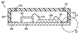
도 3a는 하부-포트형 마이크로폰 패키지(300)의 또 다른 예를 도시한다. 이 예에서, MEMS 마이크로폰 다이(301)는 다시 기판(305)을 관통하여 형성된 음향 입력 포트(303)에 인접하여 장착된다. 기판(305)은 열가소성 성형 리드(307)에 밀봉식으로 결합된다. 그러나 이 예에서 기판(305)에는 추가 전자 부품, 즉 ASIC(309)도 장착된다. 기판 상의 도전성 트레이스(311)는 리드(307)의 내표면 상의 대응 도전성 트레이스(313)와 정렬되며, 리드의 상면을 관통하여 형성된 도전성 "비아"(315)로 연장된다. 리드(307)의 상면의 외부에는 하나 이상의 전기 접촉 패드(317)가 장착된다. 제1 와이어 본드가 MEMS 마이크로폰 다이(301)를 ASIC(309)에 전자식으로 결합시키며, 제2 와이어 본드(321)가 ASIC(309)를 리드(307)의 내표면 상에 증착된 트레이스(313)를 통해서 리드(307)의 외표면 상의 접촉 패드(317)에 결합시킨다. 이런 식으로, ASIC(309)는 MEMS 마이크로폰 다이(301)의 작동을 모니터링하고 제어하며, 또한 접촉 패드(317)를 통한 외부 시스템과의 전기 통신을 촉진한다. 3A shows another example of a bottom-ported
도 3b는 도 3a에서의 인서트 "D"의 상세도를 제공함으로써 도 3a의 하부-포트형 구조의 추가 특징을 도시한다. 도 3b에 도시하듯이, 격리층(323)이 솔더 마스크에 개구(325)를 제공하며, 상기 개구에서 리드(307) 상의 도전성 트레이스(313)가 기판(305) 상의 트레이스(311)와 전자식으로 결합될 수 있다. 리드(307)를 기판(305)에 밀봉하기 위해 325에서 솔더(또는 다른 도전성 재료)가 증착될 때, 리드 트레이스(313)와 대응 기판 트레이스(311) 사이에 전기 접속부(327)가 형성된다. FIG. 3B illustrates additional features of the bottom-ported structure of FIG. 3A by providing a detailed view of insert “D” in FIG. 3A. As shown in FIG. 3B, an
도 3b에 도시하듯이, 전기 절연된 트레이스(329)가 기판의 외부 에지 주위에 도전성 링을 형성하며, 이는 공동을 음향적으로 밀봉하고 또한 리드(307) 상의 도전성 차폐층과 기판(305)의 접지부 사이에 도전성 연결을 제공하기 위해 사용된다. 이 도전성 링과 차폐 구조는 도 3c 및 도 3d에 보다 명료하게 도시되어 있다. 도 3c는 리드(307)가 기판(305)에 결합되는 지점에서의 리드(307)의 저부로부터의 횡단면도이다. 점선은 전자 통신을 위해 전자 트레이스가 증착되는 위치인 리드(307)의 내표면을 나타낸다. 도전성 차폐층은 도전성 트레이스 링(329) 위에서 리드를 통해 연장된다. 도전성 차폐층은 도 1c에 도시하듯이 리드(307)의 내표면 상에 형성될 수 있거나 또는 성형 리드(307)의 외표면 상에 증착될 수 있다. 리드의 도전성 트레이스와 능동 전자기기 사이의 전기 통신은 지점(327)에 제공되고, 차폐의 접지부는 접촉 패드(331)에 제공된다. As shown in FIG. 3B, electrically
도 3d는 기판(305) 상의 대응 도전성 접점 구조를 도시한다. 다시, 도전성 링 트레이스(329)는 접촉 패드(331)에서 리드(307)의 차폐층과 기판(305)의 접지부 사이의 전기적 결합을 제공한다. 기판(305)의 표면 상의 도전성 트레이스(311)는 도 3d에서 더 잘 볼 수 있으며, 전기 접속부(327)에서 리드(307)의 내표면 상의 트레이스와 정렬된다. 와이어 본드(321)가 ASIC(309)를 기판(305)의 전기 트레이스(311)에 연결시킨다. 3D shows a corresponding conductive contact structure on
상기 논의는 주로 기판 상에 장착된 부품과 리드의 대향 표면 상에 장착된 부품 사이의 전자 통신의 단일 경로에 집중하고 있지만, 전술한 개념은 두 개의 표면 사이 및 일부 경우에 기판과 리드의 측면 상에 장착된 디바이스 사이의 전자 통신을 위한 여러가지 수단을 제공하기 위해 사용될 수 있음을 알아야 한다. 예를 들어, 도 3d에서는, 모두 세 개의 와이어 본드(321) 각각이 ASIC(309)를 상이한 트레이스(311)에 연결하기 위해 사용된다. 각각의 트레이스는 이 트레이스가 상이한 위치에서 리드(및 리드의 내부에 형성된 대응 트레이스)와 접촉하는 지점까지 연장된다. 따라서, 도 3d의 예는 기판(305) 상에 장착된 ASIC(309)와 리드의 상면에 장착된 부품(예를 들면, 전기 접촉 패드) 사이의 전기 통신을 위해 세 개의 상이한 전기 절연된 경로를 제공한다. While the above discussion mainly focuses on a single path of electronic communication between a component mounted on a substrate and a component mounted on an opposing surface of the lead, the above concept is on the side of the substrate and the lead between two surfaces and in some cases. It should be appreciated that the present invention may be used to provide various means for electronic communication between devices mounted on the device. For example, in FIG. 3D, all three
전술한 것과 같은 MEMS 마이크로폰 패키지는 어레이로 제조될 수 있으며 단일 기판으로부터 단일화(singulate)될 수 있다. 도 4에 도시하듯이, 단일 기판 층(401)은 어레이로 배열되는 복수의 MEMS 마이크로폰 다이, 관련 회로, 및 필수 도전성 트레이스(일괄해서 403으로 도시됨)를 구비하도록 제조된다. 열가소성 성형 리드의 어레이(405)(각각 적절한 도전성 트레이스를 구비)는 기판 패키지(403)의 어레이와 정렬되고, 적소로 하강되며, 기판에 밀봉식으로 결합된다. 도 4는 기판 어레이(401) 위에 정렬되는 제1 리드 어레이(405) 및 적소로 하강된 다른 리드 어레이(407)를 도시한다. 이후 개별 패키지는 어레이로부터 단일화된다. MEMS microphone packages, such as those described above, can be manufactured in an array and can be singulated from a single substrate. As shown in FIG. 4, a
MEMS 마이크로폰 패키지의 일부 구조는 구체적으로 전술한 것과 같은 어레이-기반 제조 기술 및 단일화 공정으로부터 이득을 얻도록 설계된다. 예를 들어, 차폐 목적으로 리드의 내표면을 금속화하는 대신에, 하나 이상의 금속화된 전기 비아가, 어레이의 쏘우-스트리트(saw-street)를 따라서 배치되는 리드 어레이의 일부로서 형성될 수 있다. Some structures of MEMS microphone packages are specifically designed to benefit from array-based manufacturing techniques and singulation processes such as those described above. For example, instead of metallizing the inner surface of the lead for shielding purposes, one or more metalized electrical vias may be formed as part of a lead array disposed along the saw-street of the array. .
도 5a는 상부-포트형 MEMS 마이크로폰 패키지(500)의 하나의 이러한 구조의 예를 도시한다(패키지의 리드의 구조 및 부품을 보다 양호하게 도시하기 위해 기판은 생략되어 있음). 기준 측정은 이 예에서 여러 부품의 상대 치수를 제공한다. 리드(501)에는 MEMS 마이크로폰 다이(503)와 이것에 장착되는 ASIC(505) 양자가 제공된다. 리드(501)의 재료 내에는 일련의 도전성 트레이스(507)가 배치되며, 이는 공동이 밀봉될 때 기판과의 전기 접속을 제공한다. 전술했듯이, 리드(501)의 외표면 주위에는 도전층(509)이 배치된다. 이 도전층(509)은 기판의 접지부에 결합되며, 전술한 MEMS 마이크로폰 다이(503)의 전자기 차폐를 제공한다. 5A shows an example of one such structure of a top-ported MEMS microphone package 500 (substrate is omitted to better illustrate the structure and components of the lid of the package). Reference measurements provide the relative dimensions of the various parts in this example. The
이 예에서 도전층(509)은 리드(501)의 외표면 상에 증착되지 않는다. 대신에, 리드의 어레이[즉, 도 4의 어레이(405)]는 리드 어레이의 쏘우-스트리트를 따라서 하나 이상의 비아 어레인지를 구비하도록 제조된다. 개별 패키지가 어레이로부터 단일화될 때, 비아는 부분적으로 절취된다. 리드의 외표면 상의 도전성 비아의 잔여부는 도 5a의 도전성 차폐층(509)을 형성한다. In this example, the
도 5b는 상부-포트형 마이크로폰 패키지(500)의 리드(501)의 상부 외표면을 도시한다. 음향 포트 개구(511)는 리드(500)의 상면을 통해서 볼 수 있다. 도 5c에 도시하듯이, MEMS 마이크로폰 다이(503)는 음향 포트 개구(511)에 인접하여 리드(501)에 장착된다. ASIC(505)도 리드의 표면에 장착된다. 전술했듯이, 도전성 차폐층(509)은 각각의 단일화된 패키지(500)의 외표면을 따라서 연장된다. 5B shows the top outer surface of the
대안적으로, 리드의 외표면 상에 실질적으로 균일한 도전층을 형성하기 위해 어레이의 쏘우-스트리트에 배치되는 비아를 사용하는 대신에, 원통형 도전성 비아가 어레이 내의 쏘우-스트리트를 따라서 주기적 간격으로 배치될 수 있다. 개별 마이크로폰 패키지(500)가 단일화될 때, 원통형 비아는 이분할된다. 도 5b에 반원형 구조물(513)로서 도시되어 있는 잔여부는 기판 접지부에 결합되며, 마이크로폰 디바이스에 차폐를 제공한다. Alternatively, instead of using vias disposed in the saw-street of the array to form a substantially uniform conductive layer on the outer surface of the lid, cylindrical conductive vias are disposed at periodic intervals along the saw-street in the array. Can be. When the
또 다른 구성에서는, 마이크로폰 패키지가 단일화된 후에 도전성 차폐층(509)의 외표면 상에 격리층(515)이 증착된다. 차폐층(509)에 전기 접점을 제공하기 위해, 반원통형 절취부(513)가 리드(501)의 둘레 주위에 간격을 두고 형성된다. 도 5d에 도시하듯이, 원통형 절취부(513)는 도전성 차폐층(509)이 마이크로폰 패키지의 외부에서 부분 노출되도록 격리층(515)을 관통 절단한다. 패키지(500)의 레이아웃과 구조는 또한 도 5e에 사시도로 도시되어 있다. In another configuration, the
전술한 특정 레이아웃, 부품, 및 제조 기술은 예시적이며, 다르게 실현될 수 있다. 예를 들어, MID 리드를 형성하기 위해 사출 성형 가능한 열가소성 재료를 사용하는 것에 추가적으로, 트랜스퍼 성형 가능한 열경화성 플라스틱 재료가 사용될 수 있다. 이 재료가 MID 기술에 통상적으로 사용되지는 않지만, 이것은 일부 마이크로폰 패키지 구조에서 금속화를 위한 도금 방법을 사용함으로써 실현될 수도 있다. The specific layouts, components, and fabrication techniques described above are illustrative and can be realized differently. For example, in addition to using an injection moldable thermoplastic material to form a MID lead, a transfer moldable thermosetting plastic material may be used. Although this material is not commonly used in MID technology, this may be realized by using a plating method for metallization in some microphone package structures.
따라서, 본 발명은 무엇보다도, 기판 상에 장착된 하나 이상의 부품과 리드 상에 장착된 하나 이상의 부품 사이에 전기적 결합을 제공하는 성형 리드와 기판을 구비하는 MEMS 마이크로폰 패키지를 제공한다. 본 발명의 다양한 특징 및 장점은 하기 청구범위에 나타나 있다. Accordingly, the present invention provides, among other things, a MEMS microphone package having a substrate and a molded lead that provide electrical coupling between one or more components mounted on the substrate and one or more components mounted on the leads. Various features and advantages of the invention are set forth in the following claims.
Claims (18)
플라스틱 리드의 내표면을 따라 연장되는 제1 도전성 리드 트레이스와, 제1 도전성 리드 트레이스를 위해 사용되지 않는 위치에서 리드의 내표면 상에 전기 차폐층으로서 기판 베이스의 접지부에 전기적으로 결합되는 전기 차폐층을 구비하는 플라스틱 리드;
밀봉 공동을 형성하기 위해 상기 플라스틱 리드에 결합되는 기판 베이스로서, 상기 제1 도전성 리드 트레이스와 전기 접속부를 형성하도록 구성된 제1 도전성 기판 트레이스를 구비하는 기판 베이스;
상기 기판 베이스 상에 장착되고 상기 제1 도전성 기판 트레이스에 전기적으로 결합되는 제1 부품; 및
제2 부품으로서, 상기 플라스틱 리드 상에 장착되고 제1 도전성 리드 트레이스와 제1 도전성 기판 트레이스 사이의 전기 접속부가 제1 부품과 제2 부품 사이에 전기적 결합을 제공하도록 상기 제1 도전성 리드 트레이스에 전기적으로 결합되는 제2 부품을 포함하며,
상기 제1 도전성 리드 트레이스는 제2 부품에 근접한 제1 위치로부터 제1 도전성 기판 트레이스와 전기 접속부를 형성하는 제2 위치를 향해 밀봉 공동의 내표면을 따라 연장되고,
상기 제1 부품과 제2 부품 중 적어도 하나는 밀봉 공동의 내부에 배치되는 MEMS 마이크로폰 다이를 구비하는 마이크로폰 패키지. Microphone package,
A first conductive lead trace extending along the inner surface of the plastic lid and an electrical shield electrically coupled to the ground portion of the substrate base as an electrical shielding layer on the inner surface of the lid at a position not used for the first conductive lead trace A plastic lead having a layer;
A substrate base coupled to the plastic lead to form a sealing cavity, the substrate base comprising a first conductive substrate trace configured to form an electrical connection with the first conductive lead trace;
A first component mounted on the substrate base and electrically coupled to the first conductive substrate trace; And
A second component, mounted on the plastic lead and electrically connected to the first conductive lead trace such that an electrical connection between the first conductive lead trace and the first conductive substrate trace provides an electrical coupling between the first component and the second component. A second component coupled to the
The first conductive lead trace extends along an inner surface of the sealing cavity from a first position proximate to the second component toward a second position forming an electrical connection with the first conductive substrate trace,
At least one of the first component and the second component has a MEMS microphone die disposed inside the sealing cavity.
상기 기판 베이스를 관통하여 형성되고 전기 접촉 패드와 MEMS 마이크로폰 다이 사이에 전기적 결합을 제공하기 위해 전기 접촉 패드를 제1 도전성 기판 트레이스에 전기적으로 결합시키는 도전성 비아를 추가로 포함하는 마이크로폰 패키지. 3. The apparatus of claim 2, wherein the first component includes an electrical contact pad and is mounted on an outer surface of the substrate base;
And a conductive via formed through the substrate base and electrically coupling the electrical contact pad to the first conductive substrate trace to provide electrical coupling between the electrical contact pad and the MEMS microphone die.
리드를 관통하여 형성되고 전기 접촉 패드와 MEMS 마이크로폰 다이 사이에 전기적 결합을 제공하기 위해 전기 접촉 패드를 제1 도전성 기판 트레이스에 전기적으로 결합시키는 도전성 비아를 추가로 포함하는 마이크로폰 패키지. 6. The apparatus of claim 5, wherein the second component has an electrical contact pad and is mounted on an outer surface of the lid;
And a conductive via formed through the lead and electrically coupling the electrical contact pad to the first conductive substrate trace to provide electrical coupling between the electrical contact pad and the MEMS microphone die.
상기 리드의 외표면 상에 형성되는 제2 도전성 리드 트레이스;
상기 리드 상에 장착되고 상기 제2 도전성 리드 트레이스에 전기적으로 결합되는 제3 부품;
상기 기판 상에 형성되고, 상기 제2 도전성 리드 트레이스와 전기 접속부를 형성하도록 구성되는 제2 도전성 기판 트레이스; 및
제4 부품으로서, 상기 기판 상에 장착되고 제2 도전성 리드 트레이스와 제2 도전성 기판 트레이스 사이의 전기 접속부가 제3 부품과 제4 부품 사이에 전기적 결합을 제공하도록 상기 제2 도전성 기판 트레이스에 전기적으로 결합되는 제4 부품을 추가로 포함하는 마이크로폰 패키지. The method of claim 1,
A second conductive lead trace formed on an outer surface of the lead;
A third component mounted on the lead and electrically coupled to the second conductive lead trace;
A second conductive substrate trace formed on the substrate and configured to form an electrical connection with the second conductive lead trace; And
A fourth component, mounted on the substrate and electrically connected to the second conductive substrate trace such that an electrical connection between the second conductive lead trace and the second conductive substrate trace provides an electrical coupling between the third component and the fourth component. The microphone package further comprising a fourth component to be joined.
기판 베이스를 관통하여 형성되고 상기 제1 전기 접촉 패드와 상기 MEMS 마이크로폰 다이의 제1 접촉 핀 사이에 전기적 결합을 제공하기 위해 제1 전기 접촉 패드를 제1 도전성 기판 트레이스에 전기적으로 결합시키는 제1 도전성 비아; 및
기판 베이스를 관통하여 형성되고 상기 제2 전기 접촉 패드와 상기 MEMS 마이크로폰 다이의 제2 접촉 핀 사이에 전기적 결합을 제공하기 위해 제2 전기 접촉 패드를 제2 도전성 기판 트레이스에 전기적으로 결합시키는 제2 도전성 비아를 추가로 포함하는 마이크로폰 패키지. 11. The apparatus of claim 10, wherein the first component has a first electrical contact pad mounted on an outer surface of the substrate base and the fourth component has a second electrical contact pad mounted on an outer surface of the substrate base. ,
A first conductivity formed through the substrate base and electrically coupling the first electrical contact pad to the first conductive substrate trace to provide electrical coupling between the first electrical contact pad and the first contact pin of the MEMS microphone die Vias; And
A second conductivity formed through the substrate base and electrically coupling the second electrical contact pad to the second conductive substrate trace to provide electrical coupling between the second electrical contact pad and the second contact pin of the MEMS microphone die. Microphone package further including vias.
어레이로 배열되는 복수의 기판 베이스를 구비하는 기판 어레이를 제공하는 단계로서, 상기 복수의 기판 베이스의 각각의 기판 베이스는 제1 도전성 기판 트레이스 및 상기 제1 도전성 기판 트레이스에 전기적으로 결합되는 제1 부품을 구비하는 기판 어레이를 제공하는 단계;
어레이로 배열되는 복수의 리드를 구비하는 리드 어레이를 제공하는 단계로서, 상기 복수의 리드의 각각의 리드는 밀봉되지 않은 공동, 상기 밀봉되지 않은 공동의 내표면 상의 제1 도전성 리드 트레이스, 및 상기 제1 도전성 리드 트레이스에 전기적으로 결합되는 제2 부품을 구비하는 단계;
각각의 제1 도전성 리드 트레이스가 대응 제1 도전성 기판 트레이스와 정렬되도록 리드 어레이를 기판 어레이와 정렬시키는 단계;
각각 밀봉 공동을 구비하는 마이크로폰 패키지의 어레이를 형성하고 각각의 제1 도전성 리드 트레이스를 대응 제1 도전성 기판 트레이스와 전기적으로 연결하기 위해 기판 어레이와 리드 어레이를 밀봉식으로 결합시키는 단계; 및
상기 마이크로폰 패키지의 어레이를 쏘우-스트리트를 따라서 분리시킴으로써 마이크로폰 패키지의 어레이로부터 마이크로폰 패키지를 분리하는 단계를 포함하는 마이크로폰 패키지 제조 방법. The method of manufacturing the microphone package of claim 1,
Providing a substrate array having a plurality of substrate bases arranged in an array, each substrate base of the plurality of substrate bases having a first conductive substrate trace and a first component electrically coupled to the first conductive substrate trace Providing a substrate array having a;
Providing a lead array having a plurality of leads arranged in an array, each lead of the plurality of leads having an unsealed cavity, a first conductive lead trace on the inner surface of the unsealed cavity, and the first lead; Providing a second component electrically coupled to the first conductive lead trace;
Aligning the lead array with the substrate array such that each first conductive lead trace is aligned with a corresponding first conductive substrate trace;
Sealingly coupling the substrate array and the lead array to form an array of microphone packages each having a sealing cavity and to electrically connect each first conductive lead trace with a corresponding first conductive substrate trace; And
Separating the microphone package from the array of microphone packages by separating the array of microphone packages along a saw-street.
성형 가능한 열가소성 재료로 형성되는 성형 인터커넥트 디바이스 리드로서, 플라스틱 리드의 내표면을 따라 연장되는 도전성 리드 트레이스와, 제1 도전성 리드 트레이스를 위해 사용되지 않는 위치에서 리드의 내표면 상에 전기 차폐층으로서 기판 베이스의 접지부에 전기적으로 결합되는 전기 차폐층을 구비하는 성형 인터커넥트 디바이스 리드;
상기 성형 인터커넥트 디바이스 리드의 상면을 관통하여 형성되는 음향 포트 개구;
상기 음향 포트 개구에 인접하여 상기 성형 인터커넥트 디바이스 리드의 내표면 상에 장착되는 MEMS 마이크로폰 다이로서, 상기 도전성 리드 트레이스에 전기적으로 결합되는 MEMS 마이크로폰 다이;
밀봉 공동을 형성하기 위해 상기 성형 인터커넥트 디바이스 리드에 결합되는 베이스 기판으로서, 상기 도전성 리드 트레이스와 전기 접속부를 형성하도록 구성된 상기 밀봉 공동의 내부 상의 도전성 기판 트레이스를 구비하는 베이스 기판; 및
상기 베이스 기판의 외표면 상에 장착되고, 도전성 기판 트레이스와 도전성 리드 트레이스 사이의 전기 접속부가 전기 접촉 패드와 MEMS 마이크로폰 다이 사이에 전기적 결합을 제공하도록 상기 도전성 기판 트레이스에 전기적으로 결합되는 전기 접촉 패드를 포함하고,
상기 제1 도전성 리드 트레이스는 제2 부품에 근접한 제1 위치로부터 제1 도전성 기판 트레이스와 전기 접속부를 형성하는 제2 위치를 향해 밀봉 공동의 내표면을 따라 연장되는 상부-포트형 마이크로폰 패키지. Top-port microphone package
A molded interconnect device lead formed of a moldable thermoplastic material, the substrate comprising: a conductive lead trace extending along the inner surface of the plastic lead and a substrate as an electrical shield on the inner surface of the lead at a position not used for the first conductive lead trace A molded interconnect device lead having an electrical shield layer electrically coupled to a ground portion of the base;
An acoustic port opening formed through an upper surface of the molded interconnect device lead;
A MEMS microphone die mounted on an inner surface of the molded interconnect device lead adjacent the acoustic port opening, the MEMS microphone die electrically coupled to the conductive lead traces;
A base substrate coupled to the molded interconnect device leads to form a sealing cavity, comprising: a base substrate having conductive substrate traces on the interior of the sealing cavity configured to form electrical connections with the conductive lead traces; And
An electrical contact pad mounted on an outer surface of the base substrate and electrically coupled to the conductive substrate trace such that an electrical connection between the conductive substrate trace and the conductive lead trace provides an electrical coupling between the electrical contact pad and the MEMS microphone die. Including,
Wherein the first conductive lead trace extends along an inner surface of the sealing cavity from a first position proximate to the second component toward a second position forming an electrical connection with the first conductive substrate trace.
베이스 기판로서, 베이스 기판의 제1 표면 상에 도전성 기판 트레이스를 구비하는, 베이스 기판;
상기 베이스 기판을 관통하여 형성되는 음향 포트 개구;
상기 음향 포트 개구에 인접하여 상기 베이스 기판의 제1 표면 상에 장착되는 MEMS 마이크로폰 다이로서, 상기 도전성 기판 트레이스에 전기적으로 결합되는 MEMS 마이크로폰 다이;
성형 가능한 열가소성 재료로 형성되고 밀봉 공동을 형성하기 위해 베이스 기판에 결합되는 성형 인터커넥트 디바이스 리드로서, 베이스 기판의 제1 표면이 밀봉 공동의 내부에 위치하고, 도전성 기판 트레이스와 전기 접속부를 형성하도록 구성된 도전성 리드 트레이스를 구비하며, 상기 도전성 리드 트레이스와 중첩되지 않는 전기적 차폐를 포함하는 성형 인터커넥트 디바이스 리드; 및
상기 성형 인터커넥트 디바이스 리드의 외표면 상에 장착되고, 도전성 기판 트레이스와 도전성 리드 트레이스 사이의 전기 접속부가 전기 접촉 패드와 MEMS 마이크로폰 다이 사이에 전기적 결합을 제공하도록 상기 도전성 리드 트레이스에 전기적으로 결합되는 전기 접촉 패드 마운트를 포함하고,
상기 도전성 기판 트레이스는 전기 접속 패드에 근접한 제1 위치로부터 도전성 기판 트레이스와 도전성 리드 트레이스 사이에 전기 접속부를 형성하는 제2 위치를 향해 성형 인터커넥트 디바이스 리드의 내표면을 따라 연장되는 하부-포트형 마이크로폰 패키지. Bottom-port microphone package
A base substrate, comprising: a base substrate having conductive substrate traces on a first surface of the base substrate;
An acoustic port opening formed through the base substrate;
A MEMS microphone die mounted on a first surface of the base substrate adjacent the acoustic port opening, the MEMS microphone die electrically coupled to the conductive substrate trace;
A molded interconnect device lead formed of a moldable thermoplastic material and bonded to a base substrate to form a sealing cavity, wherein the first surface of the base substrate is positioned inside the sealing cavity and is configured to form an electrical connection with the conductive substrate trace A molded interconnect device lead having a trace, the molded interconnect device lead including an electrical shield that does not overlap the conductive lead trace; And
An electrical contact mounted on an outer surface of the molded interconnect device lead, the electrical contact between the conductive substrate trace and the conductive lead trace electrically coupled to the conductive lead trace to provide electrical coupling between the electrical contact pad and the MEMS microphone die Including pad mount,
The conductive substrate trace extends along the inner surface of the molded interconnect device lead from a first position proximate the electrical connection pad toward a second position that forms an electrical connection between the conductive substrate trace and the conductive lead trace. .
Applications Claiming Priority (3)
| Application Number | Priority Date | Filing Date | Title |
|---|---|---|---|
| US201261698801P | 2012-09-10 | 2012-09-10 | |
| US61/698,801 | 2012-09-10 | ||
| PCT/US2013/058891 WO2014040017A1 (en) | 2012-09-10 | 2013-09-10 | Mems microphone package with molded interconnect device |
Publications (2)
| Publication Number | Publication Date |
|---|---|
| KR20150054909A KR20150054909A (en) | 2015-05-20 |
| KR102062195B1 true KR102062195B1 (en) | 2020-02-11 |
Family
ID=49223891
Family Applications (1)
| Application Number | Title | Priority Date | Filing Date |
|---|---|---|---|
| KR1020157008913A Active KR102062195B1 (en) | 2012-09-10 | 2013-09-10 | Mems microphone package with molded interconnect device |
Country Status (6)
| Country | Link |
|---|---|
| US (1) | US9002038B2 (en) |
| EP (1) | EP2893713B1 (en) |
| KR (1) | KR102062195B1 (en) |
| CN (1) | CN104604248B (en) |
| TW (1) | TWI606731B (en) |
| WO (1) | WO2014040017A1 (en) |
Families Citing this family (60)
| Publication number | Priority date | Publication date | Assignee | Title |
|---|---|---|---|---|
| US8247253B2 (en) * | 2009-08-11 | 2012-08-21 | Pixart Imaging Inc. | MEMS package structure and method for fabricating the same |
| US9307328B2 (en) * | 2014-01-09 | 2016-04-05 | Knowles Electronics, Llc | Interposer for MEMS-on-lid microphone |
| US20150237429A1 (en) * | 2014-02-14 | 2015-08-20 | Knowles Electronics, Llc | Microphone In Speaker Assembly |
| US10812900B2 (en) * | 2014-06-02 | 2020-10-20 | Invensense, Inc. | Smart sensor for always-on operation |
| US20150350772A1 (en) * | 2014-06-02 | 2015-12-03 | Invensense, Inc. | Smart sensor for always-on operation |
| JP6412598B2 (en) * | 2014-06-23 | 2018-10-24 | Tdk株式会社 | Microphone and method of manufacturing a microphone |
| US9162869B1 (en) * | 2014-07-31 | 2015-10-20 | Merry Electronics (Shenzhen) Co., Ltd. | MEMS microphone package structure having non-planar substrate and method of manufacturing same |
| US9582085B2 (en) | 2014-09-30 | 2017-02-28 | Apple Inc. | Electronic devices with molded insulator and via structures |
| US9781519B2 (en) | 2014-10-29 | 2017-10-03 | Akustica, Inc. | Molded interconnect mircoelectromechanical system (MEMS) device package |
| CN107005756B (en) | 2014-10-29 | 2019-11-01 | 罗伯特·博世有限公司 | Microphone package with the spacer being molded |
| US9641940B2 (en) | 2014-11-06 | 2017-05-02 | Robert Bosch Gmbh | Metalized microphone lid with integrated wire bonding shelf |
| CN204408625U (en) * | 2015-01-21 | 2015-06-17 | 瑞声声学科技(深圳)有限公司 | Mems microphone |
| US9783412B2 (en) * | 2015-01-29 | 2017-10-10 | Unisem (M) Berhad | Method for improving manufacturability of cavity packages for direct top port MEMS microphone |
| CN105916084B (en) * | 2015-02-23 | 2019-11-12 | 因文森斯公司 | The intelligence sensor of always-on operation |
| US9554207B2 (en) | 2015-04-30 | 2017-01-24 | Shure Acquisition Holdings, Inc. | Offset cartridge microphones |
| US9565493B2 (en) | 2015-04-30 | 2017-02-07 | Shure Acquisition Holdings, Inc. | Array microphone system and method of assembling the same |
| US10291973B2 (en) | 2015-05-14 | 2019-05-14 | Knowles Electronics, Llc | Sensor device with ingress protection |
| CN107534818B (en) * | 2015-05-14 | 2020-06-23 | 美商楼氏电子有限公司 | microphone |
| KR101684526B1 (en) * | 2015-08-28 | 2016-12-08 | 현대자동차 주식회사 | Microphone and method manufacturing the same |
| CN106608613A (en) * | 2015-10-24 | 2017-05-03 | 美律电子(深圳)有限公司 | Chip package of micro-electro-mechanical system and manufacturing method of chip package |
| US9868632B2 (en) | 2016-03-24 | 2018-01-16 | Infineon Technologies Ag | Molded cavity package with embedded conductive layer and enhanced sealing |
| US20170325012A1 (en) | 2016-05-06 | 2017-11-09 | Infineon Technologies Ag | Device for detecting acoustic waves |
| DE102016113347A1 (en) * | 2016-07-20 | 2018-01-25 | Infineon Technologies Ag | METHOD FOR PRODUCING A SEMICONDUCTOR MODULE |
| JP6914540B2 (en) * | 2016-07-29 | 2021-08-04 | 国立大学法人東北大学 | Microphones, electronics and packaging methods |
| US10281485B2 (en) | 2016-07-29 | 2019-05-07 | Invensense, Inc. | Multi-path signal processing for microelectromechanical systems (MEMS) sensors |
| TW201808020A (en) * | 2016-08-24 | 2018-03-01 | 菱生精密工業股份有限公司 | MEMS microphone package structure including a substrate, a sidewall, a cover plate, a processing chip, and an acoustic wave transducer |
| US10367948B2 (en) | 2017-01-13 | 2019-07-30 | Shure Acquisition Holdings, Inc. | Post-mixing acoustic echo cancellation systems and methods |
| JP6838990B2 (en) * | 2017-02-17 | 2021-03-03 | ホシデン株式会社 | Microphone unit |
| US10361145B2 (en) * | 2017-07-18 | 2019-07-23 | Skyworks Solutions, Inc. | Through-mold openings for dual-sided packaged modules with ball grid arrays |
| WO2019060021A1 (en) * | 2017-09-22 | 2019-03-28 | Robert Bosch Gmbh | Mems microphone system |
| WO2019231632A1 (en) | 2018-06-01 | 2019-12-05 | Shure Acquisition Holdings, Inc. | Pattern-forming microphone array |
| US11297423B2 (en) | 2018-06-15 | 2022-04-05 | Shure Acquisition Holdings, Inc. | Endfire linear array microphone |
| GB2582238A (en) * | 2018-08-24 | 2020-09-23 | Atlantic Inertial Systems Ltd | Sensor packages |
| US10631100B2 (en) * | 2018-09-12 | 2020-04-21 | Infineon Technologies Ag | Micro-electrical mechanical system sensor package and method of manufacture thereof |
| CN112889296B (en) | 2018-09-20 | 2025-01-10 | 舒尔获得控股公司 | Adjustable lobe shape for microphone arrays |
| US11558693B2 (en) | 2019-03-21 | 2023-01-17 | Shure Acquisition Holdings, Inc. | Auto focus, auto focus within regions, and auto placement of beamformed microphone lobes with inhibition and voice activity detection functionality |
| WO2020191354A1 (en) | 2019-03-21 | 2020-09-24 | Shure Acquisition Holdings, Inc. | Housings and associated design features for ceiling array microphones |
| EP3942845A1 (en) | 2019-03-21 | 2022-01-26 | Shure Acquisition Holdings, Inc. | Auto focus, auto focus within regions, and auto placement of beamformed microphone lobes with inhibition functionality |
| WO2020237206A1 (en) | 2019-05-23 | 2020-11-26 | Shure Acquisition Holdings, Inc. | Steerable speaker array, system, and method for the same |
| JP7731292B2 (en) | 2019-05-31 | 2025-08-29 | シュアー アクイジッション ホールディングス インコーポレイテッド | Integrated low latency automixer with voice and noise activity detection |
| WO2021041275A1 (en) | 2019-08-23 | 2021-03-04 | Shore Acquisition Holdings, Inc. | Two-dimensional microphone array with improved directivity |
| USD943558S1 (en) | 2019-11-01 | 2022-02-15 | Shure Acquisition Holdings, Inc. | Housing for ceiling array microphone |
| USD943559S1 (en) | 2019-11-01 | 2022-02-15 | Shure Acquisition Holdings, Inc. | Housing for ceiling array microphone |
| WO2021087377A1 (en) | 2019-11-01 | 2021-05-06 | Shure Acquisition Holdings, Inc. | Proximity microphone |
| US11552611B2 (en) | 2020-02-07 | 2023-01-10 | Shure Acquisition Holdings, Inc. | System and method for automatic adjustment of reference gain |
| USD944776S1 (en) | 2020-05-05 | 2022-03-01 | Shure Acquisition Holdings, Inc. | Audio device |
| USD943552S1 (en) | 2020-05-05 | 2022-02-15 | Shure Acquisition Holdings, Inc. | Audio device |
| WO2021243368A2 (en) | 2020-05-29 | 2021-12-02 | Shure Acquisition Holdings, Inc. | Transducer steering and configuration systems and methods using a local positioning system |
| CN212324360U (en) * | 2020-06-30 | 2021-01-08 | 瑞声声学科技(深圳)有限公司 | Microphone (CN) |
| CN116918351A (en) | 2021-01-28 | 2023-10-20 | 舒尔获得控股公司 | Hybrid Audio Beamforming System |
| US12452584B2 (en) | 2021-01-29 | 2025-10-21 | Shure Acquisition Holdings, Inc. | Scalable conferencing systems and methods |
| EP4043391A1 (en) * | 2021-02-10 | 2022-08-17 | TE Connectivity Solutions GmbH | Device for supporting mems and/or asic components |
| US12308811B2 (en) * | 2021-04-19 | 2025-05-20 | Skyworks Solutions, Inc. | Method of manufacturing a cap substrate for acoustic wave device |
| DE102021113343A1 (en) * | 2021-05-21 | 2022-11-24 | duotec GmbH | Media-tight overmoulding of electronic circuit boards with external contacts |
| US12431857B2 (en) | 2021-06-30 | 2025-09-30 | Skyworks Solutions, Inc. | Acoustic wave device with acoustic obstruction structure |
| US12542123B2 (en) | 2021-08-31 | 2026-02-03 | Shure Acquisition Holdings, Inc. | Mask non-linear processor for acoustic echo cancellation |
| EP4413745A1 (en) | 2021-10-04 | 2024-08-14 | Shure Acquisition Holdings, Inc. | Networked automixer systems and methods |
| TWI795953B (en) * | 2021-10-19 | 2023-03-11 | 香港商睿克科技有限公司 | Microelectromechanical system microphone structure and manufacturing method thereof |
| EP4427465A1 (en) | 2021-11-05 | 2024-09-11 | Shure Acquisition Holdings, Inc. | Distributed algorithm for automixing speech over wireless networks |
| WO2023133513A1 (en) | 2022-01-07 | 2023-07-13 | Shure Acquisition Holdings, Inc. | Audio beamforming with nulling control system and methods |
Citations (2)
| Publication number | Priority date | Publication date | Assignee | Title |
|---|---|---|---|---|
| US20080298621A1 (en) * | 2007-06-01 | 2008-12-04 | Infineon Technologies Ag | Module including a micro-electro-mechanical microphone |
| US20120153771A1 (en) * | 2009-12-23 | 2012-06-21 | Stmicroelectronics (Malta) Ltd. | Microelectromechanical transducer and corresponding assembly process |
Family Cites Families (14)
| Publication number | Priority date | Publication date | Assignee | Title |
|---|---|---|---|---|
| CN1926919B (en) * | 2004-03-09 | 2011-01-26 | 松下电器产业株式会社 | Electret Condenser Microphone |
| JP5174673B2 (en) | 2005-10-14 | 2013-04-03 | エスティーマイクロエレクトロニクス エス.アール.エル. | Electronic device with substrate level assembly and method of manufacturing the same |
| US7763488B2 (en) | 2006-06-05 | 2010-07-27 | Akustica, Inc. | Method of fabricating MEMS device |
| TWI345289B (en) * | 2007-06-08 | 2011-07-11 | Advanced Semiconductor Eng | Microelectromechanical system package and the method for manufacturing the same |
| EP2094028B8 (en) * | 2008-02-22 | 2017-03-29 | TDK Corporation | Miniature microphone assembly with solder sealing ring |
| DE102008032319B4 (en) | 2008-07-09 | 2012-06-06 | Epcos Ag | Method for producing an MST component |
| US8193596B2 (en) | 2008-09-03 | 2012-06-05 | Solid State System Co., Ltd. | Micro-electro-mechanical systems (MEMS) package |
| US8102015B2 (en) | 2008-10-02 | 2012-01-24 | Fortemedia, Inc. | Microphone package with minimum footprint size and thickness |
| US20100086146A1 (en) | 2008-10-02 | 2010-04-08 | Fortemedia, Inc. | Silicon-based microphone package |
| CN102187685B (en) | 2008-10-14 | 2015-03-11 | 美商楼氏电子有限公司 | Microphone having multiple transducer elements |
| WO2010045088A2 (en) * | 2008-10-17 | 2010-04-22 | Knowles Electronics, Llc | Apparatus and method for reducing crosstalk within a microphone |
| DE102009007837A1 (en) | 2009-02-06 | 2010-08-19 | Epcos Ag | Sensor module and method for producing sensor modules |
| US8115283B1 (en) * | 2009-07-14 | 2012-02-14 | Amkor Technology, Inc. | Reversible top/bottom MEMS package |
| CN102958826B (en) | 2010-07-08 | 2015-12-09 | 埃普科斯股份有限公司 | MEMS microphone and the method for the manufacture of MEMS microphone |
-
2013
- 2013-09-10 KR KR1020157008913A patent/KR102062195B1/en active Active
- 2013-09-10 TW TW102132636A patent/TWI606731B/en active
- 2013-09-10 EP EP13765586.6A patent/EP2893713B1/en active Active
- 2013-09-10 US US14/022,523 patent/US9002038B2/en active Active
- 2013-09-10 CN CN201380046744.0A patent/CN104604248B/en active Active
- 2013-09-10 WO PCT/US2013/058891 patent/WO2014040017A1/en not_active Ceased
Patent Citations (2)
| Publication number | Priority date | Publication date | Assignee | Title |
|---|---|---|---|---|
| US20080298621A1 (en) * | 2007-06-01 | 2008-12-04 | Infineon Technologies Ag | Module including a micro-electro-mechanical microphone |
| US20120153771A1 (en) * | 2009-12-23 | 2012-06-21 | Stmicroelectronics (Malta) Ltd. | Microelectromechanical transducer and corresponding assembly process |
Also Published As
| Publication number | Publication date |
|---|---|
| CN104604248A (en) | 2015-05-06 |
| US9002038B2 (en) | 2015-04-07 |
| US20140072151A1 (en) | 2014-03-13 |
| EP2893713A1 (en) | 2015-07-15 |
| WO2014040017A1 (en) | 2014-03-13 |
| TWI606731B (en) | 2017-11-21 |
| CN104604248B (en) | 2018-07-24 |
| TW201415909A (en) | 2014-04-16 |
| EP2893713B1 (en) | 2020-08-12 |
| KR20150054909A (en) | 2015-05-20 |
Similar Documents
| Publication | Publication Date | Title |
|---|---|---|
| KR102062195B1 (en) | Mems microphone package with molded interconnect device | |
| US9998812B2 (en) | Surface mountable microphone package, a microphone arrangement, a mobile phone and a method for recording microphone signals | |
| US9346668B1 (en) | Molded cavity substrate MEMS package fabrication method and structure | |
| CN106331966B (en) | Microelectromechanical microphone and method for manufacturing microelectromechanical microphone | |
| US8618619B1 (en) | Top port with interposer MEMS microphone package and method | |
| US9573800B2 (en) | Pre-molded MEMS device package having conductive column coupled to leadframe and cover | |
| US20160100256A1 (en) | Acoustic Assembly and Method of Manufacturing The Same | |
| KR100966681B1 (en) | Semiconductor device, lead frame and its microphone package | |
| CN109264662B (en) | System and method for overlapping sensor packages | |
| CN102685657A (en) | Component | |
| CN105830465A (en) | Acoustic assembly and method of manufacturing the same | |
| KR20200031048A (en) | Micro-electrical mechanical system sensor package and method of manufacture thereof | |
| TW201442940A (en) | Top port MEMS cavity package and method of manufacturing same | |
| JP6311800B2 (en) | Microphone with expanded back chamber and manufacturing method | |
| CN105357616B (en) | Micro-electro-mechanical microphone packaging structure with three-dimensional substrate | |
| TW201605248A (en) | Micro electromechanical microphone package structure with stereo substrate | |
| CN101492148A (en) | Microphone package, lead frame, mold substrate, and mounting structure therefor | |
| CN109292725A (en) | Sensor device and method for making sensor device | |
| CN105592393A (en) | Metalized microphone lid with integrated wire bonding shelf | |
| CN107005756B (en) | Microphone package with the spacer being molded | |
| CN104220365B (en) | Chamber encapsulation design |
Legal Events
| Date | Code | Title | Description |
|---|---|---|---|
| PA0105 | International application |
Patent event date: 20150407 Patent event code: PA01051R01D Comment text: International Patent Application |
|
| PG1501 | Laying open of application | ||
| PA0201 | Request for examination |
Patent event code: PA02012R01D Patent event date: 20180816 Comment text: Request for Examination of Application |
|
| E902 | Notification of reason for refusal | ||
| PE0902 | Notice of grounds for rejection |
Comment text: Notification of reason for refusal Patent event date: 20190410 Patent event code: PE09021S01D |
|
| E701 | Decision to grant or registration of patent right | ||
| PE0701 | Decision of registration |
Patent event code: PE07011S01D Comment text: Decision to Grant Registration Patent event date: 20191022 |
|
| PR0701 | Registration of establishment |
Comment text: Registration of Establishment Patent event date: 20191227 Patent event code: PR07011E01D |
|
| PR1002 | Payment of registration fee |
Payment date: 20191230 End annual number: 3 Start annual number: 1 |
|
| PG1601 | Publication of registration | ||
| PR1001 | Payment of annual fee |
Payment date: 20221219 Start annual number: 4 End annual number: 4 |
|
| PR1001 | Payment of annual fee |
Payment date: 20231219 Start annual number: 5 End annual number: 5 |
|
| PR1001 | Payment of annual fee |
Payment date: 20241218 Start annual number: 6 End annual number: 6 |