KR102023924B1 - Oxide thin film transistor having array substrate for display device and method for fabricating the same - Google Patents
Oxide thin film transistor having array substrate for display device and method for fabricating the same Download PDFInfo
- Publication number
- KR102023924B1 KR102023924B1 KR1020120055683A KR20120055683A KR102023924B1 KR 102023924 B1 KR102023924 B1 KR 102023924B1 KR 1020120055683 A KR1020120055683 A KR 1020120055683A KR 20120055683 A KR20120055683 A KR 20120055683A KR 102023924 B1 KR102023924 B1 KR 102023924B1
- Authority
- KR
- South Korea
- Prior art keywords
- drain
- source
- etch stop
- oxide
- layer
- Prior art date
- Legal status (The legal status is an assumption and is not a legal conclusion. Google has not performed a legal analysis and makes no representation as to the accuracy of the status listed.)
- Active
Links
Images


Classifications
-
- H—ELECTRICITY
- H10—SEMICONDUCTOR DEVICES; ELECTRIC SOLID-STATE DEVICES NOT OTHERWISE PROVIDED FOR
- H10D—INORGANIC ELECTRIC SEMICONDUCTOR DEVICES
- H10D30/00—Field-effect transistors [FET]
- H10D30/60—Insulated-gate field-effect transistors [IGFET]
- H10D30/67—Thin-film transistors [TFT]
- H10D30/6704—Thin-film transistors [TFT] having supplementary regions or layers in the thin films or in the insulated bulk substrates for controlling properties of the device
-
- H—ELECTRICITY
- H10—SEMICONDUCTOR DEVICES; ELECTRIC SOLID-STATE DEVICES NOT OTHERWISE PROVIDED FOR
- H10D—INORGANIC ELECTRIC SEMICONDUCTOR DEVICES
- H10D30/00—Field-effect transistors [FET]
- H10D30/01—Manufacture or treatment
- H10D30/021—Manufacture or treatment of FETs having insulated gates [IGFET]
- H10D30/031—Manufacture or treatment of FETs having insulated gates [IGFET] of thin-film transistors [TFT]
-
- H—ELECTRICITY
- H10—SEMICONDUCTOR DEVICES; ELECTRIC SOLID-STATE DEVICES NOT OTHERWISE PROVIDED FOR
- H10D—INORGANIC ELECTRIC SEMICONDUCTOR DEVICES
- H10D30/00—Field-effect transistors [FET]
- H10D30/60—Insulated-gate field-effect transistors [IGFET]
- H10D30/67—Thin-film transistors [TFT]
- H10D30/6729—Thin-film transistors [TFT] characterised by the electrodes
- H10D30/673—Thin-film transistors [TFT] characterised by the electrodes characterised by the shapes, relative sizes or dispositions of the gate electrodes
-
- H—ELECTRICITY
- H10—SEMICONDUCTOR DEVICES; ELECTRIC SOLID-STATE DEVICES NOT OTHERWISE PROVIDED FOR
- H10D—INORGANIC ELECTRIC SEMICONDUCTOR DEVICES
- H10D30/00—Field-effect transistors [FET]
- H10D30/60—Insulated-gate field-effect transistors [IGFET]
- H10D30/67—Thin-film transistors [TFT]
- H10D30/674—Thin-film transistors [TFT] characterised by the active materials
- H10D30/6755—Oxide semiconductors, e.g. zinc oxide, copper aluminium oxide or cadmium stannate
-
- H—ELECTRICITY
- H10—SEMICONDUCTOR DEVICES; ELECTRIC SOLID-STATE DEVICES NOT OTHERWISE PROVIDED FOR
- H10D—INORGANIC ELECTRIC SEMICONDUCTOR DEVICES
- H10D64/00—Electrodes of devices having potential barriers
- H10D64/60—Electrodes characterised by their materials
- H10D64/62—Electrodes ohmically coupled to a semiconductor
-
- H—ELECTRICITY
- H10—SEMICONDUCTOR DEVICES; ELECTRIC SOLID-STATE DEVICES NOT OTHERWISE PROVIDED FOR
- H10D—INORGANIC ELECTRIC SEMICONDUCTOR DEVICES
- H10D99/00—Subject matter not provided for in other groups of this subclass
-
- H—ELECTRICITY
- H10—SEMICONDUCTOR DEVICES; ELECTRIC SOLID-STATE DEVICES NOT OTHERWISE PROVIDED FOR
- H10H—INORGANIC LIGHT-EMITTING SEMICONDUCTOR DEVICES HAVING POTENTIAL BARRIERS
- H10H29/00—Integrated devices, or assemblies of multiple devices, comprising at least one light-emitting semiconductor element covered by group H10H20/00
- H10H29/10—Integrated devices comprising at least one light-emitting semiconductor component covered by group H10H20/00
- H10H29/14—Integrated devices comprising at least one light-emitting semiconductor component covered by group H10H20/00 comprising multiple light-emitting semiconductor components
Landscapes
- Thin Film Transistor (AREA)
Abstract
본 발명은 산화물 박막트랜지스터, 제조방법, 이를 구비한 액정표시장치용 어레이기판 및 그 제조방법에 관한 것으로, 개시된 발명은 기판상에 형성된 게이트전극; 상기 게이트전극을 포함한 기판 전면에 형성된 게이트 절연막; 상기 게이트전극 상측의 게이트 절연막 상에 형성된 액티브층; 상기 액티브층 상에 형성된 식각정지층패턴; 상기 식각정지층패턴 상에 형성되고 서로 이격된 소스부 및 드레인부; 상기 소스부와 상기 액티브층에 접촉된 소스전극과, 상기 드레인부와 상기 액티브층에 접촉된 드레인전극;을 포함하여 구성된다.The present invention relates to an oxide thin film transistor, a manufacturing method, an array substrate for a liquid crystal display device having the same, and a manufacturing method thereof. The disclosed invention includes: a gate electrode formed on a substrate; A gate insulating film formed on an entire surface of the substrate including the gate electrode; An active layer formed on the gate insulating layer above the gate electrode; An etch stop layer pattern formed on the active layer; Source and drain portions formed on the etch stop layer pattern and spaced apart from each other; And a source electrode in contact with the source portion and the active layer, and a drain electrode in contact with the drain portion and the active layer.
Description
본 발명은 박막 트랜지스터에 관한 것으로서, 보다 상세하게는 산화물 박막 트랜지스터, 그 제조방법 및 이를 구비한 표시장치용 어레이기판 그리고 그 제조방법에 관한 것이다.The present invention relates to a thin film transistor, and more particularly, to an oxide thin film transistor, a method for manufacturing the same, an array substrate for a display device having the same, and a method for manufacturing the same.
비약적으로 성장하고 있는 평판디스플레이 시장에서 가장 큰 응용 대상으로 TV(Television) 제품이 있다. 현재 TV용 패널로서 액정디스플레이(LCD; Liquid Crystal Display)가 주축을 이루고 있는 가운데, 유기발광디스플레이도 TV로의 응용을 위해 많은 연구가 진행되고 있다.The largest application in the rapidly growing flat panel display market is TV (Television) products. Currently, liquid crystal displays (LCDs) are mainly used as TV panels, and organic light emitting displays are also being researched for application to TVs.
현재의 TV 용 디스플레이 기술의 방향을 시장에서 요구하는 주요 항목에 초점을 맞추고 있는데, 시장에서 요구하는 사항으로는 대형 TV 또는 DID(Digital Information Display), 저가격, 고화질(동영상 표현력, 고해상도, 밝기, 명암비, 새재현력)이 있다.The focus of current display technology for TVs is on the market's major demands.The market demands large TV or Digital Information Display (DID), low cost, high definition (video expression power, high resolution, brightness, contrast ratio). , New reappearance).
이러한 요건에 부합되게 하기 위해서는 유리 등의 기판의 대형화와 함께, 비용 증가 없이 우수한 성능을 갖는 디스플레이 스위칭 및 구동소자로 적용될 박막 트랜지스터(TFT; Thin Film Transistor)가 필요하다.In order to meet such requirements, a thin film transistor (TFT) to be used as a display switching and driving device having excellent performance without increasing costs, along with the enlargement of a substrate such as glass, is required.
따라서, 향후의 기술개발은 이러한 추세에 맞게 저가격으로 우수한 성능의 디스플레이 패널을 제작할 수 있는 TFT 제작 기술 확보에 초점이 맞춰져야 할 것이다.Therefore, the future development of technology should focus on securing TFT manufacturing technology that can manufacture display panels of high performance at low cost in accordance with this trend.
디스플레이의 구동 및 스위칭 소자로서 대표적인 비정질 실리콘 박막트랜지스터(a-Si TFT)는 저가의 비용으로 2m가 넘는 대형 기판상에 균일하게 형성될 수 있는 소자로서 현재 널리 쓰이는 소자이다.A typical amorphous silicon thin film transistor (a-Si TFT) as a driving and switching element of a display is a device widely used as a device that can be uniformly formed on a large substrate of more than 2 m at a low cost.
그러나, 디스플레이의 대형화 및 고화질화 추세에 따라 소자 성능 역시 고성능이 요구되어, 이동도 0.5 cm2/Vs 수준의 기존의 a-Si TFT는 한계에 다다를 것으로 판단된다.However, with the trend toward larger displays and higher image quality, device performance is also required, and the existing a-Si TFT with a mobility of 0.5 cm 2 / Vs is expected to reach its limit.
따라서, a-Si TFT보다 높은 이동도를 갖는 고성능 TFT 및 제조 기술이 필요하다. 또한, a-Si TFT는 최대의 약점으로서 동작을 계속함에 따라 소자 특성이 계속 열화되어 초기의 성능을 유지할 수 없는 신뢰성 상의 문제를 내포하고 있다.Therefore, there is a need for a high performance TFT and a manufacturing technology having higher mobility than a-Si TFT. In addition, as a-Si TFT continues to operate as its greatest weakness, the device characteristics continue to deteriorate, thereby including a reliability problem in which initial performance cannot be maintained.
이것은 a-Si TFT가 교류 구동의 LCD보다는 지속적으로 전류를 흘려 보내면서 동작하는 유기발광디스플레이(OLED; Organic Luminescene Emitted Diode)로 응용되기 힘든 주된 이유이다.This is the main reason why a-Si TFT is difficult to be applied as an organic luminescence display (OLED) that operates by continuously flowing current rather than an AC-driven LCD.
a-Si TFT 대비 월등히 높은 성능을 갖는 다결정 실리콘 박막트랜지스터 (poly-Si TFT)는 수십에서 수백 cm2/Vs의 높은 이동도를 갖기 때문에, 기존 a-Si TFT에서 실현하기 힘들었던 고화질 디스플레이에 적용할 수 있는 성능을 갖을 뿐만 아니라, a-Si TFT 대비 동작에 따른 소자특성 열화 문제가 매우 적다. 그러나, poly-Si TFT를 제작하기 위해서는 a-Si TFT에 비해 많은 수의 공정이 필요하고, 그에 다른 추가 장비 투자 역시 선행되어야 한다.Poly-Si TFTs, which have significantly higher performance than a-Si TFTs, have high mobility from tens to hundreds of cm 2 / Vs, so they can be applied to high-definition displays that were difficult to realize in conventional a-Si TFTs. In addition to the performance, the problem of deterioration of device characteristics due to operation compared to a-Si TFT is very small. However, manufacturing a poly-Si TFT requires a large number of processes compared to a-Si TFT, and other additional equipment investment must also be preceded.
따라서, p-Si TFT는 디스플레이의 고화질화나 OLED와 같은 제품에 응용되기 적합하지만, 비용 면에서는 기존 a-Si TFT에 비해 열세이므로 응용이 제한적일 수 밖에 없다. Therefore, the p-Si TFT is suitable for high-definition display and applications such as OLED, but in terms of cost is inferior to the existing a-Si TFT, the application is limited.
특히, p-Si TFT 의 경우, 제조장비의 한계나 균일도 불량과 같은 기술적인 문제로 현재까지는 1m가 넘는 대형 기판을 이용한 제조 공정이 실현되고 있지 않기 때문에, TV 제품으로의 응용이 어려운 것도, 고성능의 p-Si TFT가 쉽게 시장에 자리 잡기 힘들게 하는 요인이 되고 있다.In particular, in the case of p-Si TFT, due to technical problems such as limitations of manufacturing equipment and poor uniformity, a manufacturing process using a large substrate of more than 1 m has not been realized until now, so that application to TV products is difficult. P-Si TFTs are becoming a factor that makes it difficult to position in the market.
따라서, a-Si TFT의 장점(대형화, 저가격화, 균일도)과 poly-Si TFT의 장점(고성능, 신뢰성)을 모두 취할 수 있는 새로운 TFT기술에 대한 요구가 어느 때보다도 크며, 이에 대한 연구가 활발히 진행되고 있는데, 그 대표적인 것으로 산화물 반도체가 있다.Therefore, the demand for a new TFT technology that can take advantage of both the advantages of a-Si TFT (large size, low cost, uniformity) and the advantages of poly-Si TFT (high performance, reliability) is greater than ever. There is progress, and the representative thing is an oxide semiconductor.
이러한 산화물 반도체인 경우 비정질 실리콘(a-Si) TFT에 비해 이동도 (mobility)가 높고, 다결정 실리콘(poly-Si) TFT에 비해서는 제조 공정이 간단하고 제작 비용이 낮다는 장점이 있어, 액정디스플레이(LCD) 및 유기전계발광소자(OLED)로서의 이용 가치가 높다. Such oxide semiconductors have advantages of higher mobility than amorphous silicon (a-Si) TFTs and simpler manufacturing processes and lower manufacturing costs than polycrystalline silicon (poly-Si) TFTs. The use value as (LCD) and organic electroluminescent element (OLED) is high.
이러한 관점에서, 산화물 반도체를 이용한 종래기술에 따른 산화물 박막트랜지스터 구조에 대해 도 1 및 2를 참조하여 설명하면 다음과 같다.In this regard, the oxide thin film transistor structure according to the related art using an oxide semiconductor will be described with reference to FIGS. 1 and 2 as follows.
도 1은 종래기술에 따른 산화물 박막 트랜지스터 구조의 평면도이다.1 is a plan view of an oxide thin film transistor structure according to the prior art.
도 2는 도 1의 Ⅱ-Ⅱ선에 따른 단면도로서, 종래기술에 따른 산화물 박막 트랜지스터의 개략적인 단면도이다.FIG. 2 is a cross-sectional view taken along line II-II of FIG. 1 and is a schematic cross-sectional view of an oxide thin film transistor according to the prior art.
도 3은 도 2의 "A" 확대 단면도로서, 식각정지층과 소스전극 및 드레인전극 간 거리에 대해 개략적으로 도시한 단면도이다.3 is an enlarged cross-sectional view "A" of FIG. 2 and schematically illustrates a cross-sectional view of the distance between the etch stop layer, the source electrode, and the drain electrode.
종래기술에 따른 산화물 박막 트랜지스터(10)는, 도 1 내지 3에 도시된 바와 같이, 기판(11) 상에 일정 폭과 길이를 갖고 패턴된 게이트전극(13)과, 상기 게이트전극(13)을 포함한 기판(11) 전면에 형성된 게이트 절연막(15)과, 상기 게이트 전극(13) 상측을 포함한 게이트 절연막(15)의 상부에 형성되고 일정 모양으로 패턴 형성된 산화물 반도체로 이루어진 액티브층(17)과, 상기 액티브층(17) 상에 형성되고 일정 모양으로 패턴 형성된 식각정지층(19)과, 상기 식각정지층(19) 상부에서 서로 이격되고 상기 액티브층(17)과 게이트 절연막(15) 상부에 걸쳐 형성된 소스전극(21) 및 드레인전극(23)을 포함하여 구성된다.In the oxide
여기서, 상기 식각정지층(19)은 상기 게이트전극(13)과 액티브층(17)과 오버랩되어 있으며, 상기 액티브층(17)의 채널영역 상부에 형성된다.The
또한, 상기 소스전극(21) 및 드레인전극(27)은 상기 식각정지층(19) 상부에서 서로 이격되어 형성되고, 상기 식각정지층(19), 액티브층(17) 및 게이트 절연막 (15)에 걸쳐 형성된다. In addition, the
이때, 상기 소스전극(21)과 식각정지층(19)의 일측이 서로 오버랩되는 제1 폭(W1)과 상기 드레인전극(23)과 식각정지층(19)의 타측이 오버랩되는 제2 폭(W2)은 서로 다르게 형성된다. In this case, a first width W1 of which one side of the
이는 산화물 박막트랜지스터의 소스전극 및 드레인전극 제조 공정시에, 마스크의 오정렬(misalign)로 인해 상기 식각정지층(19) 상부에서 서로 이격되게 형성되는 소스전극(21))과 오버랩되는 식각정지층(19)의 일측 간의 제1 폭(W1)과, 드레인전극(23)과 식각정지층(19)의 타측 간의 제2 폭(W2)이 서로 다르게 형성된다. 즉, 상기 제1 폭(W1)은 제2 폭(W2)보다 길게 형성된다. 이는 소스전극 및 드레인전극 형성시에, 마스크(미도시)가 식각정지층(19)의 타측으로 오정렬되어 이동 (shift)됨으로 인해 발생하게 된다.In the manufacturing process of the source electrode and the drain electrode of the oxide thin film transistor, an etch stop layer overlapping the
특히, 산화물 박막트랜지스터 제조시에, 상기 식각정지층(19)을 형성하는 공정과 소스전극(21) 및 드레인전극(23)을 형성하는 공정이 서로 다른 마스크 공정에 의해 진행되기 때문에 상기 소스전극(21) 및 드레인전극(23)과 식각정지층(19) 간에 오정렬이 발생할 가능성이 있게 된다.In particular, when the oxide thin film transistor is manufactured, the process of forming the
따라서, 종래기술에 따른 산화물 박막트랜지스터의 경우, 이러한 상기 소스전극(21) 및 드레인전극(23)과 식각정지층(19) 간에 발생하는 오정렬로 인해, 산화물 박막트랜지스터의 온 전류(on current) 또는 문턱전압(Vth; threshold voltage)이 이동되는(shift) 문제가 나타나게 된다.Accordingly, in the oxide thin film transistor according to the related art, due to the misalignment occurring between the
또한, 종래기술에 따른 산화물 박막트랜지스터는 식각정지층(19)을 형성하는 공정과 소스전극(21) 및 드레인전극(23)을 형성하는 공정이 서로 다른 마스크 공정에 의해 진행되기 때문에, 그만큼 마스크 공정 수가 늘어나서 제작 비용이 증가하게 된다.In the oxide thin film transistor according to the related art, the process of forming the
본 발명은 종래기술의 문제점들을 해결하기 위한 것으로, 본 발명의 목적은 반도체소자 제조시의 오정렬을 방지하여 소자 특성의 균일도를 향상시키고, 마스크 수를 줄여 제조비용을 절감시킬 수 있는 산화물 박막트랜지스터, 그 제조방법, 이를 구비한 표시장치용 어레이기판 및 그 제조방법을 제공함에 있다. The present invention is to solve the problems of the prior art, an object of the present invention is to prevent the misalignment during fabrication of the semiconductor device to improve the uniformity of the device characteristics, the number of masks to reduce the oxide thin film transistor, A method of manufacturing the same, an array substrate for a display device having the same, and a method of manufacturing the same are provided.
상기 목적을 달성하기 위한 본 발명에 따른 산화물 박막트랜지스터는, 기판상에 형성된 게이트전극과; 상기 게이트전극을 포함한 기판 전면에 형성된 게이트 절연막과; 상기 게이트전극 상측의 게이트 절연막 상에 형성된 액티브층과; 상기 액티브층 상에 형성된 식각정지층과; 상기 식각정지층 상에 형성되고 서로 이격된 소스부 및 드레인부와; 상기 소스부와 상기 액티브층에 접촉된 소스전극과, 상기 드레인부와 상기 액티브층에 접촉된 드레인전극;을 포함하여 구성되는 것을 특징으로 한다.An oxide thin film transistor according to the present invention for achieving the above object comprises a gate electrode formed on a substrate; A gate insulating film formed on an entire surface of the substrate including the gate electrode; An active layer formed on the gate insulating film above the gate electrode; An etch stop layer formed on the active layer; Source and drain portions formed on the etch stop layer and spaced apart from each other; And a source electrode in contact with the source portion and the active layer, and a drain electrode in contact with the drain portion and the active layer.
상기 목적을 달성하기 위한 본 발명에 따른 산화물 박막트랜지스터 제조방법은, 기판상에 게이트전극을 형성하는 단계와; 상기 게이트전극을 포함한 기판 전면에 게이트 절연막을 형성하는 단계와; 상기 게이트전극 상측의 게이트 절연막 상에 액티브층을 형성하는 단계와; 상기 액티브층 상에 식각정지층과, 서로 이격된 소스부 및 드레인부를 형성하는 단계와; 상기 소스부와 상기 액티브층에 소스전극을 형성하고, 상기 드레인부와 상기 액티브층에 드레인전극을 형성하는 단계;를 포함하여 구성되는 것을 특징으로 한다.Oxide thin film transistor manufacturing method according to the present invention for achieving the above object comprises the steps of forming a gate electrode on the substrate; Forming a gate insulating film on an entire surface of the substrate including the gate electrode; Forming an active layer on the gate insulating film above the gate electrode; Forming an etch stop layer and source and drain portions spaced apart from each other on the active layer; And forming a source electrode on the source unit and the active layer, and forming a drain electrode on the drain unit and the active layer.
상기 목적을 달성하기 위한 본 발명의 다른 실시 예에 따른 산화물 박막트랜지스터를 구비한 표시장치용 어레이기판은, 기판상에 형성된 게이트전극과; 상기 게이트전극을 포함한 기판 전면에 형성된 게이트 절연막과; 상기 게이트전극 상측의 게이트 절연막 상에 형성된 액티브층과; 상기 액티브층 상에 형성된 식각정지층과; 상기 식각정지층 상에 형성되고 서로 이격된 소스부 및 드레인부와; 상기 소스부 및 드레인부를 포함한 기판 전면에 형성되고, 상기 액티브층을 노출시키는 소스전극 콘택홀과 드레인전극 콘택홀을 구비한 패시베이션막과; 상기 패시베이션막 상부에 형성되고, 소스전극 콘택홀을 통해 상기 소스부와 상기 액티브층에 접촉된 소스전극과, 상기 드레인전극 콘택홀을 통해 상기 드레인부와 상기 액티브층에 접촉된 드레인전극과; 상기 패시베이션막 상에 형성되고, 상기 드레인전극으로부터 연장된 화소전극과 이 화소전극과 이격된 공통전극;을 포함하여 구성되는 것을 특징으로 한다.According to another aspect of the present invention, an array substrate for a display device having an oxide thin film transistor includes: a gate electrode formed on a substrate; A gate insulating film formed on an entire surface of the substrate including the gate electrode; An active layer formed on the gate insulating film above the gate electrode; An etch stop layer formed on the active layer; Source and drain portions formed on the etch stop layer and spaced apart from each other; A passivation film formed over the substrate including the source and drain portions, the passivation layer including a source electrode contact hole and a drain electrode contact hole exposing the active layer; A source electrode formed on the passivation layer and in contact with the source portion and the active layer through a source electrode contact hole, and a drain electrode in contact with the drain portion and the active layer through the drain electrode contact hole; And a common electrode formed on the passivation layer, the pixel electrode extending from the drain electrode, and the common electrode spaced apart from the pixel electrode.
상기 목적을 달성하기 위한 본 발명의 다른 실시 예에 따른 산화물 박막트랜지스터를 구비한 표시장치용 어레이기판 제조방법은, 기판상에 게이트전극을 형성하는 단계와; 상기 게이트전극을 포함한 기판 전면에 게이트 절연막을 형성하는 단계와; 상기 게이트전극 상측의 게이트 절연막 상에 액티브층을 형성하는 단계와; 상기 액티브층 상에 식각정지층과 서로 이격된 소스부 및 드레인부을 형성하는 단계와; 상기 소스부 및 드레인부를 포함한 기판 전면에 상기 액티브층을 노출시키는 소스전극 콘택홀과 드레인전극 콘택홀을 구비한 패시베이션막을 형성하는 단계와; 상기 소스전극 콘택홀을 통해 상기 소스부와 상기 액티브층에 접촉된 소스전극과, 상기 드레인전극 콘택홀을 통해 상기 드레인부와 상기 액티브층에 접촉된 드레인전극을 형성하는 단계 및; 상기 드레인전극으로부터 연장된 화소전극과 이 화소전극과 이격된 공통전극을 형성하는 단계;를 포함하여 구성되는 것을 특징으로 한다.According to another aspect of the present invention, there is provided a method of manufacturing an array substrate for a display device having an oxide thin film transistor, the method including: forming a gate electrode on a substrate; Forming a gate insulating film on an entire surface of the substrate including the gate electrode; Forming an active layer on the gate insulating film above the gate electrode; Forming a source portion and a drain portion spaced apart from the etch stop layer on the active layer; Forming a passivation film including a source electrode contact hole and a drain electrode contact hole exposing the active layer on the entire surface of the substrate including the source part and the drain part; Forming a source electrode in contact with the source portion and the active layer through the source electrode contact hole, and a drain electrode in contact with the drain portion and the active layer through the drain electrode contact hole; And forming a pixel electrode extending from the drain electrode and a common electrode spaced apart from the pixel electrode.
본 발명에 따른 산화물 박막트랜지스터, 그 제조방법, 이를 구비한 표시장치용 어레이기판 및 그 제조방법에 따르면, 다음과 같은 효과가 있다.According to the oxide thin film transistor according to the present invention, a method of manufacturing the same, an array substrate for a display device having the same, and a method of manufacturing the same, the following effects are obtained.
본 발명에 따른 산화물 박막트랜지스터, 그 제조방법, 이를 구비한 표시장치용 어레이기판 및 그 제조방법에 따르면, 소스부 및 드레인부 또는 데이터배선 형성시에 하프톤 마스크(half-ton mask)를 적용하여 소스부 및 드레인부 또는 데이터배선과 식각정지층을 동일 마스크로 형성할 수 있어, 소스부 및 드레인부와 식각정지층이 오정렬되는 현상이 제거된다.According to the oxide thin film transistor according to the present invention, a method of manufacturing the same, an array substrate for a display device having the same, and a method of manufacturing the same, a half-ton mask is applied when a source part and a drain part or a data line are formed. The source and drain portions or the data wiring and the etch stop layer can be formed with the same mask, thereby eliminating the phenomenon that the source and drain portions and the etch stop layer are misaligned.
또한, 본 발명에 따른 산화물 박막트랜지스터, 그 제조방법, 이를 구비한 표시장치용 어레이기판 및 그 제조방법에 따르면, 소스부 및 드레인부와 식각 정지층을 하프톤 마스크를 적용하여 동일 마스크로 형성할 수 있기 때문에, 소스부 및 드레인부와 식각정지층 간의 정렬 마진(align margin)이 감소함에 따라 단채널(short channel) 구현이 가능하게 된다.In addition, according to the oxide thin film transistor according to the present invention, a method of manufacturing the same, an array substrate for a display device having the same, and a method of manufacturing the same, a source mask, a drain capacitor, and an etch stop layer may be formed using a halftone mask. Since the alignment margin between the source and drain portions and the etch stop layer is reduced, the short channel may be realized.
그리고, 본 발명에 따른 산화물 박막트랜지스터, 그 제조방법, 이를 구비한 표시장치용 어레이기판 및 그 제조방법에 따르면, 소스부 및 드레인부 또는 데이터배선 형성시에 하프톤 마스크(half-ton mask)를 적용하여 소스부 및 드레인부 또는 데이터배선과 식각정지층을 동일 마스크로 형성할 수 있어 포토 오정렬(photo misalign)이 제거됨에 따라, 공정 변동에 따른 소자 특성 차 및 기판 내의 소자 균일성 (uniformity) 특성이 향상된다. In addition, according to the oxide thin film transistor according to the present invention, a method of manufacturing the same, an array substrate for a display device having the same, and a method of manufacturing the same, a half-ton mask is formed when a source part and a drain part or a data line are formed. The source and drain portions, or the data wiring and the etch stop layer can be formed using the same mask so that photo misalignment is eliminated, and thus device uniformity characteristics and substrate uniformity characteristics due to process variations are eliminated. This is improved.
더욱이, 본 발명에 따른 산화물 박막트랜지스터, 그 제조방법, 이를 구비한 표시장치용 어레이기판 및 그 제조방법에 따르면, 소스부 및 드레인부와 식각 정지층을 하프톤 마스크를 적용하여 동일 마스크로 형성할 수 있기 때문에 마스크 수가 저감되어 제조 비용이 절감되는 효과가 있다.Furthermore, according to the oxide thin film transistor according to the present invention, a method of manufacturing the same, an array substrate for a display device having the same, and a method of manufacturing the same, the source and drain portions and the etch stop layer may be formed using the same mask using a halftone mask. Since the number of masks can be reduced, manufacturing cost can be reduced.
도 1은 종래기술에 따른 산화물 박막 트랜지스터 구조의 평면도이다.
도 2는 도 1의 Ⅱ-Ⅱ선에 따른 단면도로서, 종래기술에 따른 산화물 박막 트랜지스터의 개략적인 단면도이다.
도 3은 도 2의 "A" 확대 단면도로서, 식각정지층과 소스전극 및 드레인전극 간 거리에 대해 개략적으로 도시한 단면도이다.
도 4는 본 발명에 따른 산화물 박막 트랜지스터 구조의 평면도이다.
도 5는 도 4의 Ⅴ-Ⅴ선에 따른 단면도로서, 본 발명에 따른 산화물 박막 트랜지스터의 개략적인 단면도이다.
도 6a 내지 6j는 본 발명에 따른 산화물 박막 트랜지스터의 제조공정 단면도들이다.
도 7은 본 발명의 다른 실시 예에 따른 산화물 박막트랜지스터를 구비한 표시장치용 어레이기판의 개략적인 단면도이다.
도 8a 내지 8k는 본 발명의 다른 실시 예에 따른 산화물 박막트랜지스터를 구비한 표시장치용 어레이기판의 제조 공정 단면도들이다.
도 9는 본 발명의 또 다른 실시 예에 따른 산화물 박막트랜지스터를 구비한 표시장치용 어레이기판의 개략적인 단면도이다.
도 10a 내지 10k는 본 발명의 또 다른 실시 예에 따른 산화물 박막트랜지스터를 구비한 표시장치용 어레이기판의 제조 공정 단면도들이다.1 is a plan view of an oxide thin film transistor structure according to the prior art.
FIG. 2 is a cross-sectional view taken along line II-II of FIG. 1 and is a schematic cross-sectional view of an oxide thin film transistor according to the prior art.
3 is an enlarged cross-sectional view "A" of FIG. 2 and schematically illustrates a cross-sectional view of the distance between the etch stop layer, the source electrode, and the drain electrode.
4 is a plan view of an oxide thin film transistor structure according to the present invention.
5 is a cross-sectional view taken along the line VV of FIG. 4 and is a schematic cross-sectional view of the oxide thin film transistor according to the present invention.
6A to 6J are cross-sectional views illustrating a process of manufacturing an oxide thin film transistor according to the present invention.
7 is a schematic cross-sectional view of an array substrate for a display device having an oxide thin film transistor according to another exemplary embodiment of the present invention.
8A through 8K are cross-sectional views illustrating a manufacturing process of an array substrate for a display device having an oxide thin film transistor according to another exemplary embodiment of the present invention.
9 is a schematic cross-sectional view of an array substrate for a display device having an oxide thin film transistor according to still another embodiment of the present invention.
10A through 10K are cross-sectional views illustrating a manufacturing process of an array substrate for a display device having an oxide thin film transistor according to another exemplary embodiment of the present invention.
이하, 본 발명의 바람직한 실시 예에 따른 산화물 박막트랜지스터 구조에 대해 첨부된 도면을 참조하여 상세히 설명한다.Hereinafter, an oxide thin film transistor structure according to a preferred embodiment of the present invention will be described in detail with reference to the accompanying drawings.
도 4는 본 발명에 따른 산화물 박막 트랜지스터 구조의 평면도이다.4 is a plan view of an oxide thin film transistor structure according to the present invention.
도 5는 도 4의 Ⅴ-Ⅴ선에 따른 단면도로서, 본 발명에 따른 산화물 박막 트랜지스터의 개략적인 단면도이다.5 is a cross-sectional view taken along the line VV of FIG. 4 and is a schematic cross-sectional view of the oxide thin film transistor according to the present invention.
본 발명에 따른 산화물 박막트랜지스터(100)는, 도 4 및 5에 도시된 바와 같이, 기판(101)상에 형성된 게이트전극(103a)과; 상기 게이트전극(103a)을 포함한 기판 전면에 형성된 게이트 절연막(107)과; 상기 게이트전극(103a) 상측의 게이트 절연막(107) 상에 형성된 액티브층(109)과; 상기 액티브층(109) 상에 형성된 식각정지층패턴(113a)과; 상기 식각정지층패턴(113a) 상에 형성되고 서로 이격된 소스부 (115a) 및 드레인부(115b)와; 상기 소스부(115a)와 상기 액티브층(109)에 접촉된 소스전극(123a)과, 상기 드레인부(115b)와 상기 액티브층(109)에 접촉된 드레인전극(123b);을 포함하여 구성된다.Oxide
여기서, 상기 게이트전극(103a)은 실리콘, 유리, 플라스틱 또는 다른 적절한 물질을 포함하여 이루어지거나, 금속 또는 다른 적절한 도전 물질로 이루어질 수 있다. 예컨대, 상기 게이트전극(103a)으로는, 산화인듐주석(Indium Tin Oxide; ITO), 산화갈륨아연(Indium Gallium Zinc Oixde; GZO), 산화인듐갈륨아연(Indium Gallium Zinc Oxide; IGZO), 산화인듐갈륨(Indium Gallium Oixe; IGO), 산화인듐아연 (Indium Zinc Oxide; IZO), 산화인듐아연(Indium Zinc Oxide; IZO) 및 산화인듐 (In2O3)으로 이루어지는 그룹으로부터 선택되는 어느 하나 또는 이들의 2 이상의 조합 또는 다른 적절한 물질을 포함할 수도 있다. 또는 상기 게이트 전극(103a)의 형성 물질로는, 알루미늄(Al), 텅스텐(W), 구리 (Cu), 몰리브덴(Mo), 크롬(Cr), 티타늄 (Ti), 몰리텅스텐(MoW), 몰리티타늄 (MoTi), 구리/몰리티타늄 (Cu/MoTi)을 포함하는 도전성 금속 그룹 중에서 선택된 적어도 어느 하나 또는 이들의 2 이상의 조합 또는 다른 적절한 물질을 포함할 수도 있다. The
또한, 상기 게이트 절연막(107)으로는 산화실리콘(SiO2), 질화실리콘(SiNx), 산화지르코늄(ZrO2), 산화하프늄(HfO2), 산화티타늄(TiO2), 산화탄탈륨(Ta2O5), 바륨-스트론튬-티타늄-산소화합물(Ba-Sr-Ti-O) 및 비스머스-아연-니오븀-산소 화합물(Bi-Zn-Nb-O)로 이루어지는 그룹으로부터 선택되는 어느 하나 또는 이들의 2 이상의 조합 또는 다른 적절한 물질을 포함할 수도 있다.In addition, the
그리고, 상기 액티브층(109)은 소스전극(123a)과 드레인전극(123b) 사이에 전자가 이동하는 채널을 형성하기 위한 층으로서, 저온 다결정 실리콘(Low Temperature Poly Silicon; 이하 LTPS라 함) 또는 비정질 실리콘(a-Si) 재질 대신에 실리콘(Si)을 포함하는 산화물 반도체로 이루어진다.The
이때, 상기 산화물 반도체로는, 게르마늄 (Ge), 주석(Sn), 납(Pb), 인듐 (In), 티타늄(Ti), 갈륨(Ga) 및 알루미늄(Al)으로 이루어지는 그룹으로부터 선택된 하나 이상의 물질 및 아연(Zn)을 포함하는 산화물 반도체에 실리콘 (Si)이 첨가된 물질로 이루어질 수 있다. 예컨대, 상기 액티브패턴(109a)은 인듐아연 복합 산화물(InZnO)에 실리콘 이온이 첨가된 실리콘 산화인듐아연(Si-InZnO: SIZO)으로 이루어질 수도 있다.In this case, the oxide semiconductor, at least one material selected from the group consisting of germanium (Ge), tin (Sn), lead (Pb), indium (In), titanium (Ti), gallium (Ga) and aluminum (Al). And silicon (Si) added to the oxide semiconductor including zinc (Zn). For example, the active pattern 109a may be formed of silicon indium zinc oxide (Si-InZnO: SIZO) in which silicon ions are added to indium zinc complex oxide (InZnO).
상기 액티브층(109)이 SIZO로 이루어지는 경우, 액티브층에서 아연(Zn), 인듐(In) 및 실리콘(Si) 원자의 전체 함량 대비 실리콘(Si) 원자 함량의 조성비는 약 0.001 중량%(wt%) 내지 약 30 wt%일 수도 있다. 실리콘(Si) 원자 함량이 높아질수록 전자 생성을 제어하는 역할이 강해져서, 이동도가 낮아질 수 있으나, 그 소자의 안정성은 더 좋아질 수 있다.When the
한편, 상기 액티브층(109)으로는, 전술한 물질 외에 리튬(Li) 또는 칼륨(K)과 같은 I족 원소, 마그네슘(Mg), 칼슘(Ca) 또는 스트론튬(Sr)과 같은 Ⅱ족 원소, 갈륨(Ga), 알루미늄(Al), 인듐(In) 또는 이트륨(Y)과 같은 Ⅲ족 원소, 티타늄(Ti), 지르코늄(Zr), 실리콘(Si), 주석(Sn) 또는 게르마늄(Ge)과 같은 Ⅳ족 원소, 탄탈륨(Ta), 바나듐(V), 니오븀(Nb) 또는 안티몬(Sb)과 같은 Ⅴ족 원소, 또는 란티늄(La), 세륨(Ce), 프라세오디뮴(Pr), 네오디뮴(Nd), 프로메튬(Pm), 사마륨 (Sm), 유로퓸(Eu), 가돌리듐(Gd), 터븀(Tb), 디스프로슘(Dy), 홀뮴(Ho), 어븀(Er), 툴륨(Tm), 이터븀(Yb) 또는 루테듐(Lu)과 같은 란탄(Ln) 계열 원소 등이 더 포함될 수도 있다.On the other hand, the
또한, 상기 식각정지층패턴(113a)은 산화실리콘(SiO2)과 질화실리콘 (SiNx)으로 이루어진 무기 절연물질 중에서 어느 하나를 선택하여 사용한다.In addition, the etch
그리고, 상기 소스부(115a) 및 드레인부(115b)는 상기 게이트전극(103a)과 마찬가지로 금속 또는 다른 적절한 도전물질을 포함하여 이루어질 수 있다. 예컨대, 상기 소스부(115a) 및 드레인부(115b)는 산화인듐주석(Indium Tin Oxide; ITO), 산화갈륨아연(Indium Gallium Zinc Oixde; GZO), 산화인듐갈륨아연(Indium Gallium Zinc Oxide; IGZO), 산화인듐갈륨(Indium Gallium Oixe; IGO), 산화인듐아연 (Indium Zinc Oxide; IZO), 산화인듐아연(Indium Zinc Oxide; IZO) 및 산화인듐 (In2O3)으로 이루어지는 그룹으로부터 선택되는 어느 하나 또는 이들의 2 이상의 조합 또는 다른 적절한 물질을 포함할 수도 있다. 또는, 상기 소스부(115a) 및 드레인부(115b)는 알루미늄(Al), 텅스텐(W), 구리 (Cu), 몰리브덴(Mo), 크롬(Cr), 티타늄 (Ti), 몰리텅스텐(MoW), 몰리티타늄 (MoTi), 구리/몰리티타늄 (Cu/MoTi)을 포함하는 도전성 금속 그룹 중에서 선택된 적어도 어느 하나 또는 이들의 2 이상의 조합 또는 다른 적절한 물질을 포함할 수도 있다.The
특히, 상기 소스부(115a) 및 드레인부(115b)는 상기 식각정지층패턴(113a)의 영역 내에 한정하여 형성되며, 이들 소스부(115a) 및 드레인부(115b)는 상기 식각정지층패턴(113a) 영역 내에서 이격되어 형성된다. 이는 산화물 박막트랜지스터 제조시에, 하프톤 마스크를 이용한 마스크 공정시에, 상기 소스부(115a) 및 드레인부 (115b)가 상기 식각정지층패턴(113a)과 동일 마스크로 형성되기 때문에 가능하게 된다. In particular, the
따라서, 상기 소스부(115a) 및 드레인부(115b)와 오버랩되는 식각정지층패턴 (113a)의 일측 및 타측 간 제1 폭(W1)과 제2 폭(W2)은 항상 동일하게 유지됨으로써, 상기 소스부(115a) 및 드레인부(115b)과 식각정지층패턴(113a) 간의 오정렬(misalign)이 방지된다.Accordingly, the first width W1 and the second width W2 between one side and the other side of the etch
그리고, 상기 소스전극(123a) 및 드레인전극(123b)은 동일한 물질로 형성되는데, 상기 소스전극(123a) 및 드레인전극(123b)으로는, 상기 게이트전극(103a)과 마찬가지로 금속 또는 다른 적절한 도전물질을 포함하여 이루어질 수 있다. 예컨대, 상기 소스전극(123a) 및 드레인전극(123b)은 산화인듐주석(Indium Tin Oxide; ITO), 산화갈륨아연(Indium Gallium Zinc Oixde; GZO), 산화인듐갈륨아연 (Indium Gallium Zinc Oxide; IGZO), 산화인듐갈륨(Indium Gallium Oixe; IGO), 산화인듐아연 (Indium Zinc Oxide; IZO), 산화인듐아연(Indium Zinc Oxide; IZO) 및 산화인듐 (In2O3)으로 이루어지는 그룹으로부터 선택되는 어느 하나 또는 이들의 2 이상의 조합 또는 다른 적절한 물질을 포함할 수도 있다. 또는, 상기 소스전극 (123a) 및 드레인전극(123b)은 알루미늄(Al), 텅스텐(W), 구리 (Cu), 몰리브덴 (Mo), 크롬(Cr), 티타늄 (Ti), 몰리텅스텐(MoW), 몰리티타늄 (MoTi), 구리/몰리티타늄 (Cu/MoTi)을 포함하는 도전성 금속 그룹 중에서 선택된 적어도 어느 하나 또는 이들의 2 이상의 조합 또는 다른 적절한 물질을 포함할 수도 있다.The
특히, 상기 소스전극(123a) 및 드레인전극(123b) 각각은 소스부(115a) 및 드레인부(115b) 상부를 포함한 상기 액티브층(109)의 노출된 부분과도 접촉되도록 형성됨으로써, 채널이 상기 소스전극(123a) 및 드레인전극(123b)과 연결되어 박막트랜지스터 특성이 나타나게 된다.In particular, each of the
이와 같은 구성으로 이루어지는 본 발명에 따른 산화물 박막트랜지스터 제조방법에 대해 첨부된 도면을 참조하여 상세히 설명한다.An oxide thin film transistor manufacturing method according to the present invention having such a configuration will be described in detail with reference to the accompanying drawings.
도 6a 내지 6j는 본 발명에 따른 산화물 박막 트랜지스터의 제조공정 단면도들이다.6A to 6J are cross-sectional views illustrating a process of manufacturing an oxide thin film transistor according to the present invention.
도 6a를 참조하면, 기판(101)상에 게이트전극용 제1 도전물질을 스퍼터링방법으로 증착하여 제1 도전층(103)을 형성하고, 그 위에 제1 감광막(미도시)을 도포한 후, 포토리소그라피 공정기술을 이용한 제1 마스크 공정을 통해 상기 제1 감광막(미도시)을 패터닝하여 제1 감광막패턴(105)을 형성한다.Referring to FIG. 6A, after depositing a first conductive material for a gate electrode on a
이때, 상기 제1 도전층(103)은 실리콘, 유리, 플라스틱 또는 다른 적절한 물질을 포함하여 이루어지거나, 금속 또는 다른 적절한 도전 물질로 이루어질 수 있다. 예컨대, 상기 게이트전극(103a)으로는, 산화인듐주석(Indium Tin Oxide; ITO), 산화갈륨아연(Indium Gallium Zinc Oixde; GZO), 산화인듐갈륨아연(Indium Gallium Zinc Oxide; IGZO), 산화인듐갈륨(Indium Gallium Oixe; IGO), 산화인듐아연 (Indium Zinc Oxide; IZO), 산화인듐아연(Indium Zinc Oxide; IZO) 및 산화인듐 (In2O3)으로 이루어지는 그룹으로부터 선택되는 어느 하나 또는 이들의 2 이상의 조합 또는 다른 적절한 물질을 포함할 수도 있다. 또는 상기 제1 도전층(103)의 형성 물질로는, 알루미늄(Al), 텅스텐(W), 구리 (Cu), 몰리브덴(Mo), 크롬(Cr), 티타늄 (Ti), 몰리텅스텐(MoW), 몰리티타늄 (MoTi), 구리/몰리티타늄 (Cu/MoTi)을 포함하는 도전성 금속 그룹 중에서 선택된 적어도 어느 하나 또는 이들의 2 이상의 조합 또는 다른 적절한 물질을 포함할 수도 있다. In this case, the first
그 다음, 도 6b를 참조하면, 상기 제1 감광막패턴(105)을 식각 마스크로 상기 제1 도전층(103)을 선택적으로 식각하여 게이트전극(103a)을 형성한다. 6B, the first
이어서, 도 6c를 참조하면, 상기 제1 감광막패턴(105)을 제거하고, 상기 게이트전극(103a)을 포함한 기판 전면에 게이트 절연막(107)을 형성한다. 이때, 상기 게이트 절연막(107)으로는 산화실리콘(SiO2), 질화실리콘(SiNx), 산화지르코늄 (ZrO2), 산화하프늄(HfO2), 산화티타늄(TiO2), 산화탄탈륨(Ta2O5), 바륨-스트론튬-티타늄-산소화합물(Ba-Sr-Ti-O) 및 비스머스-아연-니오븀-산소 화합물(Bi-Zn-Nb-O)로 이루어지는 그룹으로부터 선택되는 어느 하나 또는 이들의 2 이상의 조합 또는 다른 적절한 물질을 포함할 수도 있다.Subsequently, referring to FIG. 6C, the first
이어서, 상기 게이트 절연막(107) 상에 산화물 반도체 물질을 이용하여 반도체층(미도시)을 형성하고, 그 위에 제2 감광막(미도시)을 도포한다. Subsequently, a semiconductor layer (not shown) is formed on the
그 다음, 도면에는 도시하지 않았지만, 포토리소그라피 공정기술을 이용한 제2 마스크 공정을 통해 상기 제2 감광막(미도시)을 패터닝하여 제2 감광막패턴 (미도시)을 형성한다.Next, although not shown in the drawing, the second photoresist film (not shown) is patterned through a second mask process using a photolithography process technology to form a second photoresist pattern (not shown).
이어서, 도 6c를 참조하면, 상기 제2 감광막패턴(미도시)을 식각 마스크로 상기 반도체층(미도시)을 선택적으로 제거하여, 상기 게이트전극(103a) 상측의 게이트 절연막(107) 상에 액티브층(109)을 형성한다. 이때, 상기 액티브층(109)은 소스전극(123a)과 드레인전극(123b) 사이에 전자가 이동하는 채널을 형성하기 위한 층으로서, 저온 다결정 실리콘(Low Temperature Poly Silicon; 이하 LTPS라 함) 또는 비정질 실리콘(a-Si) 재질 대신에 실리콘(Si)을 포함하는 산화물 반도체로 이루어진다.Subsequently, referring to FIG. 6C, the semiconductor layer (not shown) is selectively removed using the second photoresist pattern (not shown) as an etch mask to be active on the
이때, 상기 산화물 반도체로는, 게르마늄 (Ge), 주석(Sn), 납(Pb), 인듐 (In), 티타늄(Ti), 갈륨(Ga) 및 알루미늄(Al)으로 이루어지는 그룹으로부터 선택된 하나 이상의 물질 및 아연(Zn)을 포함하는 산화물 반도체에 실리콘 (Si)이 첨가된 물질로 이루어질 수 있다. 예컨대, 상기 액티브패턴(109a)은 인듐아연 복합 산화물(InZnO)에 실리콘 이온이 첨가된 실리콘 산화인듐아연(Si-InZnO: SIZO)으로 이루어질 수도 있다.In this case, the oxide semiconductor, at least one material selected from the group consisting of germanium (Ge), tin (Sn), lead (Pb), indium (In), titanium (Ti), gallium (Ga) and aluminum (Al). And silicon (Si) added to the oxide semiconductor including zinc (Zn). For example, the active pattern 109a may be formed of silicon indium zinc oxide (Si-InZnO: SIZO) in which silicon ions are added to indium zinc complex oxide (InZnO).
상기 액티브층(109)이 SIZO로 이루어지는 경우, 액티브층에서 아연(Zn), 인듐(In) 및 실리콘(Si) 원자의 전체 함량 대비 실리콘(Si) 원자 함량의 조성비는 약 0.001 중량%(wt%) 내지 약 30 wt%일 수도 있다. 실리콘(Si) 원자 함량이 높아질수록 전자 생성을 제어하는 역할이 강해져서, 이동도가 낮아질 수 있으나, 그 소자의 안정성은 더 좋아질 수 있다.When the
한편, 상기 액티브층(109)으로는, 전술한 물질 외에 리튬(Li) 또는 칼륨(K)과 같은 I족 원소, 마그네슘(Mg), 칼슘(Ca) 또는 스트론튬(Sr)과 같은 Ⅱ족 원소, 갈륨(Ga), 알루미늄(Al), 인듐(In) 또는 이트륨(Y)과 같은 Ⅲ족 원소, 티타늄(Ti), 지르코늄(Zr), 실리콘(Si), 주석(Sn) 또는 게르마늄(Ge)과 같은 Ⅳ족 원소, 탄탈륨(Ta), 바나듐(V), 니오븀(Nb) 또는 안티몬(Sb)과 같은 Ⅴ족 원소, 또는 란티늄(La), 세륨(Ce), 프라세오디뮴(Pr), 네오디뮴(Nd), 프로메튬(Pm), 사마륨 (Sm), 유로퓸(Eu), 가돌리듐(Gd), 터븀(Tb), 디스프로슘(Dy), 홀뮴(Ho), 어븀(Er), 툴륨(Tm), 이터븀(Yb) 또는 루테듐(Lu)과 같은 란탄(Ln) 계열 원소 등이 더 포함될 수도 있다.On the other hand, the
그 다음, 도 6d를 참조하면, 상기 액티브층(109)을 포함한 기판 전면에 식각정지층(113)과 제2 도전층(115)을 차례로 적층하고, 그 위에 다시 제3 감광막(117)을 도포한다. 이때, 상기 식각정지층(113)은 산화실리콘(SiO2)과 질화실리콘 (SiNx)으로 이루어진 무기 절연물질 중에서 어느 하나를 선택하여 사용한다.Next, referring to FIG. 6D, the
또한, 상기 제2 도전층(115)은 상기 게이트전극(103a)과 마찬가지로 금속 또는 다른 적절한 도전물질을 포함하여 이루어질 수 있다. 예컨대, 상기 제2 도전층 (117)은 산화인듐주석(Indium Tin Oxide; ITO), 산화갈륨아연(Indium Gallium Zinc Oixde; GZO), 산화인듐갈륨아연(Indium Gallium Zinc Oxide; IGZO), 산화인듐갈륨 (Indium Gallium Oixe; IGO), 산화인듐아연 (Indium Zinc Oxide; IZO), 산화인듐아연(Indium Zinc Oxide; IZO) 및 산화인듐 (In2O3)으로 이루어지는 그룹으로부터 선택되는 어느 하나 또는 이들의 2 이상의 조합 또는 다른 적절한 물질을 포함할 수도 있다. 또는, 상기 제2 도전층(115)은 알루미늄(Al), 텅스텐(W), 구리 (Cu), 몰리브덴(Mo), 크롬(Cr), 티타늄 (Ti), 몰리텅스텐(MoW), 몰리티타늄 (MoTi), 구리/몰리티타늄 (Cu/MoTi)을 포함하는 도전성 금속 그룹 중에서 선택된 적어도 어느 하나 또는 이들의 2 이상의 조합 또는 다른 적절한 물질을 포함할 수도 있다.In addition, like the
이어서, 하프톤 마스크(Half-Ton Mask)(121)을 이용한 포토리소그라피 공정기술을 통해 노광 공정을 실시한다. 이때, 상기 하프톤 마스크(121)는 제1 광차단패턴(121a)과 제2 광차단패턴(121b)을 포함하고 있는데, 상기 제1 광차단패턴 (121a)은 광을 전부 차단하는 역할을 담당하고, 상기 제2 광차단패턴(121b)은 광의 일부는 투과시키고, 나머지는 차단하는 역할을 담당한다.Subsequently, an exposure process is performed through a photolithography process technology using a half-
그 다음, 도 6e를 참조하면, 상기 노광 공정을 통해 광이 투과된 제3 감광막 (117) 부분을 현상 공정을 통해 제거하여, 두께가 다른 제3 감광막패턴(117a, 117b)을 형성한다. 이때, 두께가 얇은 제3 감광막패턴(117b)은 상기 액티브층 (109)의 채널영역 상부에 위치하며, 두께가 두꺼운 제3 감광막패턴(117a)은 후속 공정에서 형성될 소스부 및 드레인부 상부에 위치하게 된다.Next, referring to FIG. 6E, a portion of the third
이어서, 도 6f에 도시된 바와 같이, 상기 제3 감광막패턴(117a, 117b)을 식각 마스크로 상기 제2 도전층(115)과 식각정지층(113)을 선택적으로 식각하여 식각정지층패턴(113a)을 형성한다. 이때, 상기 식각정지층패턴(113a)은 상기 액티브층 (109) 보다 면적이 작으며, 상기 액티브층(109)의 일부는 외부로 노출된 상태가 된다.Subsequently, as shown in FIG. 6F, the second
그 다음, 도 6g를 참조하면, 상기 제3 감광막패턴(117a, 117b) 중에서, 상기 제3 감광막패턴(117b)이 완전 제거될 때까지 에싱(Ashing) 공정을 실시한다. 이때, 상기 제3 감광막패턴(117a) 일부도 함께 제거된다. 또한, 상기 제3 감광막패턴 (117b)이 완전 제거됨으로 인해, 그 하부의 제2 도전층(115) 부분이 외부로 노출된다.6G, an ashing process is performed until the
이어서, 도 6h를 참조하면, 상기 제3 감광막패턴(117a)을 식각 마스크로 상기 제2 도전층(115)의 노출된 부분을 식각하여, 서로 이격된 소스부(115a) 및 드레인부(115b)를 형성한다. 이때, 상기 소스부(115a) 및 드레인부(115b)는 상기 식각정지층패턴(113a)의 영역 내에 한정하여 형성되며, 이들 소스부(115a) 및 드레인부 (115b)는 상기 식각정지층패턴(113a) 영역 내에서 이격되어 형성된다. 이는 산화물 박막트랜지스터 제조시에, 하프톤 마스크를 이용한 마스크 공정시에, 상기 소스부 (115a) 및 드레인부 (115b)가 상기 식각정지층패턴(113a)과 동일 마스크로 형성되기 때문에 가능하게 된다. 6H, exposed portions of the second
따라서, 상기 소스부(115a) 및 드레인부(115b)와 오버랩되는 식각정지층패턴 (113a)의 일측 및 타측 간 제1 폭(W1)과 제2 폭(W2)은 항상 동일하게 유지됨으로 써, 상기 소스부(115a) 및 드레인부(115b)과 식각정지층패턴(113a) 간의 오정렬 (misalign)이 방지된다.Therefore, since the first width W1 and the second width W2 between one side and the other side of the etch
그 다음, 도면에는 도시하지 않았지만, 상기 소스부(115a) 및 드레인부 (115b)를 포함한 기판 전면에 제3 도전층(123)을 스퍼터링 방법으로 증착하고, 그 위에 제4 감광막(미도시)을 도포한다. 이때, 상기 제3 도전층(123)으로는, 상기 게이트전극(103a)과 마찬가지로 금속 또는 다른 적절한 도전물질을 포함하여 이루어질 수 있다. 예컨대, 상기 제3 도전층(123)은 산화인듐주석(Indium Tin Oxide; ITO), 산화갈륨아연(Indium Gallium Zinc Oixde; GZO), 산화인듐갈륨아연 (Indium Gallium Zinc Oxide; IGZO), 산화인듐갈륨(Indium Gallium Oixe; IGO), 산화인듐아연 (Indium Zinc Oxide; IZO), 산화인듐아연(Indium Zinc Oxide; IZO) 및 산화인듐 (In2O3)으로 이루어지는 그룹으로부터 선택되는 어느 하나 또는 이들의 2 이상의 조합 또는 다른 적절한 물질을 포함할 수도 있다. 또는, 상기 제3 도전층(123)은 알루미늄(Al), 텅스텐(W), 구리 (Cu), 몰리브덴 (Mo), 크롬(Cr), 티타늄 (Ti), 몰리텅스텐(MoW), 몰리티타늄 (MoTi), 구리/몰리티타늄 (Cu/MoTi)을 포함하는 도전성 금속 그룹 중에서 선택된 적어도 어느 하나 또는 이들의 2 이상의 조합 또는 다른 적절한 물질을 포함할 수도 있다.Next, although not shown, a third
이어서, 도 6i를 참조하면, 포토리소그라피 공정기술을 이용한 제4 마스크 공정을 통해 상기 제4 감광막(미도시)을 패터닝하여, 제4 감광막패턴(125)을 형성한다.6I, the fourth photoresist layer (not shown) is patterned through a fourth mask process using a photolithography process technology to form a fourth
그 다음, 도 6j를 참조하면, 상기 제4 감광막패턴(125)을 식각마스크로, 상기 제3 도전층(123)을 선택적으로 식각하여, 상기 소스부(115a)와 상기 액티브층 (109)에 접촉된 소스전극(123a)과, 상기 드레인부(115b)와 상기 액티브층(109)에 접촉된 드레인전극(123b)을 동일 마스크로 형성함으로써, 본 발명에 따른 산화물 박막트랜지스터 제조공정을 완료한다. 이때, 상기 소스전극(123a) 및 드레인전극(123b)은 각각 소스부(115a) 및 드레인부(115b) 상부를 포함한 상기 액티브층(109)의 노출된 부분과도 접촉되도록 형성됨으로써, 채널이 상기 소스전극(123a) 및 드레인전극 (123b)과 연결되어 박막트랜지스터 특성이 나타나게 된다.Next, referring to FIG. 6J, the
이상에서와 같이, 본 발명에 따르면, 소스부 및 드레인부 또는 데이터배선 형성시에 하프톤 마스크(half-ton mask)를 적용하여 소스부 및 드레인부 또는 데이터배선과 식각정지층을 동일 마스크로 형성할 수 있어, 소스부 및 드레인부와 식각정지층이 오정렬되는 현상이 제거된다.As described above, according to the present invention, the source and drain portions or the data wiring and the etch stop layer are formed by the same mask by applying a half-ton mask when the source and drain portions or the data wiring are formed. This eliminates the phenomenon that the source and drain portions and the etch stop layer are misaligned.
또한, 본 발명에 따르면, 소스부 및 드레인부와 식각 정지층을 하프톤 마스크를 적용하여 동일 마스크로 형성할 수 있기 때문에, 소스부 및 드레인부와 식각정지층 간의 정렬 마진(align margin)이 감소함에 따라 단채널(short channel) 구현이 가능하게 된다.In addition, according to the present invention, since the source portion, the drain portion, and the etch stop layer may be formed in the same mask by applying a halftone mask, the alignment margin between the source portion, the drain portion, and the etch stop layer is reduced. As a result, short channel implementation is possible.
그리고, 본 발명에 따르면, 소스부 및 드레인부 또는 데이터배선 형성시에 하프톤 마스크(half-ton mask)를 적용하여 소스부 및 드레인부 또는 데이터배선과 식각정지층을 동일 마스크로 형성할 수 있어 포토 오정렬(photo misalign)이 제거됨에 따라, 공정 변동에 따른 소자 특성 차 및 기판 내의 소자 균일성 (uniformity) 특성이 향상된다. According to the present invention, the source and drain portions or the data wiring and the etch stop layer may be formed using the same mask by applying a half-ton mask when the source and drain portions or the data wiring are formed. As photo misalignment is eliminated, device characteristic differences due to process variations and device uniformity characteristics in the substrate are improved.
더욱이, 본 발명에 따른 산화물 박막트랜지스터, 그 제조방법, 이를 구비한 표시장치용 어레이기판 및 그 제조방법에 따르면, 소스부 및 드레인부와 식각 정지층을 하프톤 마스크를 적용하여 동일 마스크로 형성할 수 있기 때문에 마스크 수가 저감되어 제조 비용이 절감되는 효과가 있다.Furthermore, according to the oxide thin film transistor according to the present invention, a method of manufacturing the same, an array substrate for a display device having the same, and a method of manufacturing the same, the source and drain portions and the etch stop layer may be formed using the same mask using a halftone mask. Since the number of masks can be reduced, manufacturing cost can be reduced.
따라서, 본 발명에 따른 산화물 박막트랜지스터 및 그 제조방법은, 액티브층 이 실리콘을 포함하는 산화물 반도체로 이루어지므로 높은 전자 이동도를 가지며, 생산 단가가 낮은 이점이 있다. 또한, 상기 액티브층의 제조 공정은 상온에서도 수행 가능하므로 공정을 용이하게 할 수 있다.Accordingly, the oxide thin film transistor and the method of manufacturing the same according to the present invention have an advantage of high electron mobility and low production cost since the active layer is made of an oxide semiconductor including silicon. In addition, the manufacturing process of the active layer may be performed at room temperature, thereby facilitating the process.
본 발명에 따른 산화물 박막트랜지스터 구조는, 액정표시장치 (Liquid Crystal Display; 이하 LCD라 함), 유기발광 다이오드(Organic Luminescence Emitted Diode; 이하 OLED라 함) 등 평판 디스플레이의 구동 소자 또는 스위칭 소자나, 메모리 소자의 주변 회로 구성을 위한 소자 등 다양한 전자 소자에 적용될 수 있다.The oxide thin film transistor structure according to the present invention may be a driving device or switching device of a flat panel display such as a liquid crystal display (hereinafter referred to as LCD), an organic light emitting diode (hereinafter referred to as OLED), or a memory. It can be applied to various electronic devices such as devices for the peripheral circuit configuration of the device.
한편, 본 발명의 다른 실시 예에 따른 산화물 박막트랜지스터를 구비한 액정표시장치용 어레이기판 구조에 대해 도 7을 참조하여 설명하면 다음과 같다.Meanwhile, a structure of an array substrate for a liquid crystal display device having an oxide thin film transistor according to another embodiment of the present invention will be described with reference to FIG. 7.
도 7은 본 발명의 다른 실시 예에 따른 산화물 박막트랜지스터를 구비한 표시장치용 어레이기판의 개략적인 단면도이다.7 is a schematic cross-sectional view of an array substrate for a display device having an oxide thin film transistor according to another exemplary embodiment of the present invention.
여기서, 본 발명의 다른 실시 예에 따른 산화물 박막트랜지스터를 구비한 액정표시장치용 어레이기판 구조는 횡전계 모드(In-Plane Switching Mode) 의 액정표시장치에 적용하는 경우를 예로 들어 설명하기로 한다.Here, an array substrate structure for a liquid crystal display device having an oxide thin film transistor according to another embodiment of the present invention will be described by taking an example of applying the liquid crystal display device in an in-plane switching mode.
본 발명의 다른 실시 예에 따른 산화물 박막트랜지스터를 구비한 액정표시장치용 어레이기판은, 도 7에 도시된 바와 같이, 기판(201)상에 형성된 게이트전극 (203a)과; 상기 게이트전극(203a)을 포함한 기판 전면에 형성된 게이트 절연막 (207)과; 상기 게이트전극(203a) 상측의 게이트 절연막(207) 상에 형성된 액티브층 (209)과; 상기 액티브층(209) 상에 형성된 식각정지층패턴(213a)과; 상기 식각정지층패턴(213a) 상에 형성되고 서로 이격된 소스부(215a) 및 드레인부(215b)와; 상기 소스부(215a) 및 드레인부(215b)를 포함한 기판 전면에 형성되고, 상기 액티브층 (209)을 노출시키는 소스전극 콘택홀(미도시, 도 8i의 225a 참조)과 드레인전극 콘택홀(미도시, 도 8i의 225b 참조)을 구비한 패시베이션막(223)과; 상기 패시베이션막 (223) 상에 형성되고, 상기 소스전극 콘택홀을 통해 상기 소스부(215a)와 상기 액티브층(209)에 접촉된 소스전극(227a)과, 상기 드레인전극 콘택홀을 통해 상기 드레인부(215b)와 상기 액티브층(209)에 접촉된 드레인전극(227b)과; 상기 패시베이션막(223) 상에 형성되고, 상기 드레인전극 (227b)으로부터 연장되어 분기된 화소전극(227c)과 이 화소전극(227c)과 이격된 다수의 분기된 공통전극(227d);을 포함하여 구성된다.According to another exemplary embodiment of the present invention, an array substrate for an LCD device including an oxide thin film transistor may include: a
여기서, 상기 게이트전극(203a)은 실리콘, 유리, 플라스틱 또는 다른 적절한 물질을 포함하여 이루어지거나, 금속 또는 다른 적절한 도전 물질로 이루어질 수 있다. 예컨대, 상기 게이트전극(203a)으로는, 산화인듐주석(Indium Tin Oxide; ITO), 산화갈륨아연(Indium Gallium Zinc Oixde; GZO), 산화인듐갈륨아연(Indium Gallium Zinc Oxide; IGZO), 산화인듐갈륨(Indium Gallium Oixe; IGO), 산화인듐아연 (Indium Zinc Oxide; IZO), 산화인듐아연(Indium Zinc Oxide; IZO) 및 산화인듐 (In2O3)으로 이루어지는 그룹으로부터 선택되는 어느 하나 또는 이들의 2 이상의 조합 또는 다른 적절한 물질을 포함할 수도 있다. 또는 상기 게이트 전극(203a)의 형성 물질로는, 알루미늄(Al), 텅스텐(W), 구리 (Cu), 몰리브덴(Mo), 크롬(Cr), 티타늄 (Ti), 몰리텅스텐(MoW), 몰리티타늄 (MoTi), 구리/몰리티타늄 (Cu/MoTi)을 포함하는 도전성 금속 그룹 중에서 선택된 적어도 어느 하나 또는 이들의 2 이상의 조합 또는 다른 적절한 물질을 포함할 수도 있다. Here, the
또한, 상기 게이트 절연막(207)으로는 산화실리콘(SiO2), 질화실리콘(SiNx), 산화지르코늄(ZrO2), 산화하프늄(HfO2), 산화티타늄(TiO2), 산화탄탈륨(Ta2O5), 바륨-스트론튬-티타늄-산소화합물(Ba-Sr-Ti-O) 및 비스머스-아연-니오븀-산소 화합물(Bi-Zn-Nb-O)로 이루어지는 그룹으로부터 선택되는 어느 하나 또는 이들의 2 이상의 조합 또는 다른 적절한 물질을 포함할 수도 있다.In addition, the
그리고, 상기 액티브층(209)은 소스전극(227a)과 드레인전극(227b) 사이에 전자가 이동하는 채널을 형성하기 위한 층으로서, 저온 다결정 실리콘(Low Temperature Poly Silicon; 이하 LTPS라 함) 또는 비정질 실리콘(a-Si) 재질 대신에 실리콘(Si)을 포함하는 산화물 반도체로 이루어진다.The
이때, 상기 산화물 반도체로는, 게르마늄 (Ge), 주석(Sn), 납(Pb), 인듐 (In), 티타늄(Ti), 갈륨(Ga) 및 알루미늄(Al)으로 이루어지는 그룹으로부터 선택된 하나 이상의 물질 및 아연(Zn)을 포함하는 산화물 반도체에 실리콘 (Si)이 첨가된 물질로 이루어질 수 있다. 예컨대, 상기 액티브층(109)은 인듐아연 복합 산화물 (InZnO)에 실리콘 이온이 첨가된 실리콘 산화인듐아연(Si-InZnO: SIZO)으로 이루어질 수도 있다.In this case, the oxide semiconductor, at least one material selected from the group consisting of germanium (Ge), tin (Sn), lead (Pb), indium (In), titanium (Ti), gallium (Ga) and aluminum (Al). And silicon (Si) added to the oxide semiconductor including zinc (Zn). For example, the
상기 액티브층(209)이 SIZO로 이루어지는 경우, 액티브층에서 아연(Zn), 인듐(In) 및 실리콘(Si) 원자의 전체 함량 대비 실리콘(Si) 원자 함량의 조성비는 약 0.001 중량%(wt%) 내지 약 30 wt%일 수도 있다. 실리콘(Si) 원자 함량이 높아질수록 전자 생성을 제어하는 역할이 강해져서, 이동도가 낮아질 수 있으나, 그 소자의 안정성은 더 좋아질 수 있다.When the
한편, 상기 액티브층(209)으로는, 전술한 물질 외에 리튬(Li) 또는 칼륨(K)과 같은 I족 원소, 마그네슘(Mg), 칼슘(Ca) 또는 스트론튬(Sr)과 같은 Ⅱ족 원소, 갈륨(Ga), 알루미늄(Al), 인듐(In) 또는 이트륨(Y)과 같은 Ⅲ족 원소, 티타늄(Ti), 지르코늄(Zr), 실리콘(Si), 주석(Sn) 또는 게르마늄(Ge)과 같은 Ⅳ족 원소, 탄탈륨(Ta), 바나듐(V), 니오븀(Nb) 또는 안티몬(Sb)과 같은 Ⅴ족 원소, 또는 란티늄(La), 세륨(Ce), 프라세오디뮴(Pr), 네오디뮴(Nd), 프로메튬(Pm), 사마륨 (Sm), 유로퓸(Eu), 가돌리듐(Gd), 터븀(Tb), 디스프로슘(Dy), 홀뮴(Ho), 어븀(Er), 툴륨(Tm), 이터븀(Yb) 또는 루테듐(Lu)과 같은 란탄(Ln) 계열 원소 등이 더 포함될 수도 있다.Meanwhile, the
또한, 상기 식각정지층패턴(213a)은 산화실리콘(SiO2)과 질화실리콘 (SiNx)으로 이루어진 무기 절연물질 중에서 어느 하나를 선택하여 사용한다.In addition, the etch
그리고, 상기 소스부(215a) 및 드레인부(215b)는 상기 게이트전극(203a)과 마찬가지로 금속 또는 다른 적절한 도전물질을 포함하여 이루어질 수 있다. 예컨대, 상기 소스부(215a) 및 드레인부(215b)는 산화인듐주석(Indium Tin Oxide; ITO), 산화갈륨아연(Indium Gallium Zinc Oixde; GZO), 산화인듐갈륨아연(Indium Gallium Zinc Oxide; IGZO), 산화인듐갈륨(Indium Gallium Oixe; IGO), 산화인듐아연 (Indium Zinc Oxide; IZO), 산화인듐아연(Indium Zinc Oxide; IZO) 및 산화인듐 (In2O3)으로 이루어지는 그룹으로부터 선택되는 어느 하나 또는 이들의 2 이상의 조합 또는 다른 적절한 물질을 포함할 수도 있다. 또는, 상기 소스부(215a) 및 드레인부(215b)는 알루미늄(Al), 텅스텐(W), 구리 (Cu), 몰리브덴(Mo), 크롬(Cr), 티타늄 (Ti), 몰리텅스텐(MoW), 몰리티타늄 (MoTi), 구리/몰리티타늄 (Cu/MoTi)을 포함하는 도전성 금속 그룹 중에서 선택된 적어도 어느 하나 또는 이들의 2 이상의 조합 또는 다른 적절한 물질을 포함할 수도 있다.The
특히, 상기 소스부(215a) 및 드레인부(215b)는 상기 식각정지층패턴(213a)의 영역 내에 한정하여 형성되며, 이들 소스부(215a) 및 드레인부(215b)는 상기 식각정지층패턴(213a) 영역 내에서 이격되어 형성된다. 이는 산화물 박막트랜지스터 제조시에, 하프톤 마스크를 이용한 마스크 공정시에, 상기 소스부(215a) 및 드레인부 (215b)가 상기 식각정지층패턴(213a)과 동일 마스크로 형성되기 때문에 가능하게 된다. In particular, the
따라서, 상기 소스부(215a) 및 드레인부(215b)와 오버랩되는 식각정지층패턴 (213a)의 일측 및 타측 간 제1 폭(W1)과 제2 폭(W2)은 항상 동일하게 유지됨으로써, 상기 소스부(215a) 및 드레인부(215b)과 식각정지층패턴(213a) 간의 오정렬(misalign)이 방지된다.Therefore, the first width W1 and the second width W2 between one side and the other side of the etch
그리고, 상기 소스전극(223a) 및 드레인전극(223b)은 상기 드레인전극 (223b)으로부터 연장되어 다수의 분기된 화소전극(227c)과 공통전극(227d)으로도 사용되어야 하기 때문에 투명한 도전 물질로 이루어지는데, 상기 투명한 도전 물질로는 ITO (Indium Tin Oxide), IZO(Indium Zinc Oxide)를 포함한 투명한 물질 그룹 중에서 선택된 어느 하나를 사용한다. Since the source electrode 223a and the drain electrode 223b extend from the drain electrode 223b and must also be used as the plurality of
특히, 상기 소스전극(223a) 및 드레인전극(223b)은 각각 소스부(215a) 및 드레인부(215b) 상부를 포함한 상기 액티브층(209)의 노출된 부분과도 접촉되도록 형성됨으로써, 채널이 상기 소스전극(223a) 및 드레인전극(223b)와 연결되어 박막트랜지스터 특성이 나타나게 된다.In particular, the source electrode 223a and the drain electrode 223b are formed to be in contact with an exposed portion of the
한편, 이와 같은 구성으로 이루어지는 본 발명의 다른 실시 예에 따른 산화물 박막트랜지스터를 구비한 액정표시장치용 어레이기판 제조방법에 대해 첨부된 도면을 참조하여 상세히 설명한다.Meanwhile, a method of manufacturing an array substrate for a liquid crystal display device having an oxide thin film transistor according to another embodiment of the present invention having such a configuration will be described in detail with reference to the accompanying drawings.
도 8a 내지 8k는 본 발명의 다른 실시 예에 따른 산화물 박막 트랜지스터를 구비한 액정표시장치용 어레이기판의 제조공정 단면도들이다.8A through 8K are cross-sectional views illustrating manufacturing processes of an array substrate for a liquid crystal display device having an oxide thin film transistor according to another exemplary embodiment of the present invention.
도 8a를 참조하면, 기판(201)상에 게이트전극용 제1 도전물질을 스퍼터링방법으로 증착하여 제1 도전층(203)을 형성하고, 그 위에 제1 감광막(미도시)을 도포한 후, 포토리소그라피 공정기술을 이용한 제1 마스크 공정을 통해 상기 제1 감광막(미도시)을 패터닝하여 제1 감광막패턴(205)을 형성한다.Referring to FIG. 8A, after depositing a first conductive material for a gate electrode on a
이때, 상기 제1 도전층(203)은 실리콘, 유리, 플라스틱 또는 다른 적절한 물질을 포함하여 이루어지거나, 금속 또는 다른 적절한 도전 물질로 이루어질 수 있다. 예컨대, 상기 게이트전극(203a)으로는, 산화인듐주석(Indium Tin Oxide; ITO), 산화갈륨아연(Indium Gallium Zinc Oixde; GZO), 산화인듐갈륨아연(Indium Gallium Zinc Oxide; IGZO), 산화인듐갈륨(Indium Gallium Oixe; IGO), 산화인듐아연 (Indium Zinc Oxide; IZO), 산화인듐아연(Indium Zinc Oxide; IZO) 및 산화인듐 (In2O3)으로 이루어지는 그룹으로부터 선택되는 어느 하나 또는 이들의 2 이상의 조합 또는 다른 적절한 물질을 포함할 수도 있다. 또는 상기 제1 도전층(203)의 형성 물질로는, 알루미늄(Al), 텅스텐(W), 구리 (Cu), 몰리브덴(Mo), 크롬(Cr), 티타늄 (Ti), 몰리텅스텐(MoW), 몰리티타늄 (MoTi), 구리/몰리티타늄 (Cu/MoTi)을 포함하는 도전성 금속 그룹 중에서 선택된 적어도 어느 하나 또는 이들의 2 이상의 조합 또는 다른 적절한 물질을 포함할 수도 있다. In this case, the first
그 다음, 도 8b를 참조하면, 상기 제1 감광막패턴(205)을 식각 마스크로 상기 제1 도전층(203)을 선택적으로 식각하여 게이트전극(203a)을 형성한다. Next, referring to FIG. 8B, the first
이어서, 도 8c를 참조하면, 상기 제1 감광막패턴(205)을 제거하고, 상기 게이트전극(203a)을 포함한 기판 전면에 게이트 절연막(207)을 형성한다. 이때, 상기 게이트 절연막(207)으로는 산화실리콘(SiO2), 질화실리콘(SiNx), 산화지르코늄 (ZrO2), 산화하프늄(HfO2), 산화티타늄(TiO2), 산화탄탈륨(Ta2O5), 바륨-스트론튬-티타늄-산소화합물(Ba-Sr-Ti-O) 및 비스머스-아연-니오븀-산소 화합물(Bi-Zn-Nb-O)로 이루어지는 그룹으로부터 선택되는 어느 하나 또는 이들의 2 이상의 조합 또는 다른 적절한 물질을 포함할 수도 있다.Subsequently, referring to FIG. 8C, the first
이어서, 상기 게이트 절연막(207) 상에 산화물 반도체 물질을 이용하여 반도체층(미도시)을 형성하고, 그 위에 제2 감광막(미도시)을 도포한다. Subsequently, a semiconductor layer (not shown) is formed on the
그 다음, 도면에는 도시하지 않았지만, 포토리소그라피 공정기술을 이용한 제2 마스크 공정을 통해 상기 제2 감광막(미도시)을 패터닝하여 제2 감광막패턴 (미도시)을 형성한다.Next, although not shown in the drawing, the second photoresist film (not shown) is patterned through a second mask process using a photolithography process technology to form a second photoresist pattern (not shown).
이어서, 도 8c를 참조하면, 상기 제2 감광막패턴(미도시)을 식각 마스크로 상기 반도체층(미도시)을 선택적으로 제거하여, 상기 게이트전극(203a) 상측의 게이트 절연막(207) 상에 액티브층(209)을 형성한다. 이때, 상기 액티브층(209)은 소스전극(미도시)과 드레인전극(미도시) 사이에 전자가 이동하는 채널을 형성하기 위한 층으로서, 저온 다결정 실리콘(Low Temperature Poly Silicon; 이하 LTPS라 함) 또는 비정질 실리콘(a-Si) 재질 대신에 실리콘(Si)을 포함하는 산화물 반도체로 이루어진다.Subsequently, referring to FIG. 8C, the semiconductor layer (not shown) may be selectively removed using the second photoresist layer pattern (not shown) as an etch mask, and thus active on the
이때, 상기 산화물 반도체로는, 게르마늄 (Ge), 주석(Sn), 납(Pb), 인듐 (In), 티타늄(Ti), 갈륨(Ga) 및 알루미늄(Al)으로 이루어지는 그룹으로부터 선택된 하나 이상의 물질 및 아연(Zn)을 포함하는 산화물 반도체에 실리콘 (Si)이 첨가된 물질로 이루어질 수 있다. 예컨대, 상기 액티브패턴(109a)은 인듐아연 복합 산화물(InZnO)에 실리콘 이온이 첨가된 실리콘 산화인듐아연(Si-InZnO: SIZO)으로 이루어질 수도 있다.In this case, the oxide semiconductor, at least one material selected from the group consisting of germanium (Ge), tin (Sn), lead (Pb), indium (In), titanium (Ti), gallium (Ga) and aluminum (Al). And silicon (Si) added to the oxide semiconductor including zinc (Zn). For example, the active pattern 109a may be formed of silicon indium zinc oxide (Si-InZnO: SIZO) in which silicon ions are added to indium zinc complex oxide (InZnO).
상기 액티브층(209)이 SIZO로 이루어지는 경우, 액티브층에서 아연(Zn), 인듐(In) 및 실리콘(Si) 원자의 전체 함량 대비 실리콘(Si) 원자 함량의 조성비는 약 0.001 중량%(wt%) 내지 약 30 wt%일 수도 있다. 실리콘(Si) 원자 함량이 높아질수록 전자 생성을 제어하는 역할이 강해져서, 이동도가 낮아질 수 있으나, 그 소자의 안정성은 더 좋아질 수 있다.When the
한편, 상기 액티브층(209)으로는, 전술한 물질 외에 리튬(Li) 또는 칼륨(K)과 같은 I족 원소, 마그네슘(Mg), 칼슘(Ca) 또는 스트론튬(Sr)과 같은 Ⅱ족 원소, 갈륨(Ga), 알루미늄(Al), 인듐(In) 또는 이트륨(Y)과 같은 Ⅲ족 원소, 티타늄(Ti), 지르코늄(Zr), 실리콘(Si), 주석(Sn) 또는 게르마늄(Ge)과 같은 Ⅳ족 원소, 탄탈륨(Ta), 바나듐(V), 니오븀(Nb) 또는 안티몬(Sb)과 같은 Ⅴ족 원소, 또는 란티늄(La), 세륨(Ce), 프라세오디뮴(Pr), 네오디뮴(Nd), 프로메튬(Pm), 사마륨 (Sm), 유로퓸(Eu), 가돌리듐(Gd), 터븀(Tb), 디스프로슘(Dy), 홀뮴(Ho), 어븀(Er), 툴륨(Tm), 이터븀(Yb) 또는 루테듐(Lu)과 같은 란탄(Ln) 계열 원소 등이 더 포함될 수도 있다.Meanwhile, the
그 다음, 도 8d를 참조하면, 상기 액티브층(209)을 포함한 기판 전면에 식각정지층(213)과 제2 도전층(215)을 차례로 적층하고, 그 위에 다시 제3 감광막(217)을 도포한다. 이때, 상기 식각정지층(213)은 산화실리콘(SiO2)과 질화실리콘 (SiNx)으로 이루어진 무기 절연물질 중에서 어느 하나를 선택하여 사용한다.Next, referring to FIG. 8D, the
또한, 상기 제2 도전층(215)은 상기 게이트전극(203a)과 마찬가지로 금속 또는 다른 적절한 도전물질을 포함하여 이루어질 수 있다. 예컨대, 상기 제2 도전층 (117)은 산화인듐주석(Indium Tin Oxide; ITO), 산화갈륨아연(Indium Gallium Zinc Oixde; GZO), 산화인듐갈륨아연(Indium Gallium Zinc Oxide; IGZO), 산화인듐갈륨 (Indium Gallium Oixe; IGO), 산화인듐아연 (Indium Zinc Oxide; IZO), 산화인듐아연(Indium Zinc Oxide; IZO) 및 산화인듐 (In2O3)으로 이루어지는 그룹으로부터 선택되는 어느 하나 또는 이들의 2 이상의 조합 또는 다른 적절한 물질을 포함할 수도 있다. 또는, 상기 제2 도전층(215)은 알루미늄(Al), 텅스텐(W), 구리 (Cu), 몰리브덴(Mo), 크롬(Cr), 티타늄 (Ti), 몰리텅스텐(MoW), 몰리티타늄 (MoTi), 구리/몰리티타늄 (Cu/MoTi)을 포함하는 도전성 금속 그룹 중에서 선택된 적어도 어느 하나 또는 이들의 2 이상의 조합 또는 다른 적절한 물질을 포함할 수도 있다.In addition, like the
이어서, 하프톤 마스크(Half-Ton Mask)(221)를 이용한 포토리소그라피 공정기술을 통해 노광 공정을 실시한다. 이때, 상기 하프톤 마스크(221)는 제1 광차단패턴(221a)과 제2 광차단패턴(221b)을 포함하고 있는데, 상기 제1 광차단패턴 (221a)은 광을 전부 차단하는 역할을 담당하고, 상기 제2 광차단패턴(221b)은 광의 일부는 투과시키고, 나머지는 차단하는 역할을 담당한다.Subsequently, an exposure process is performed through a photolithography process technology using a half-
그 다음, 도 8e를 참조하면, 상기 노광 공정을 통해 광이 투과된 제3 감광막 (217) 부분을 현상 공정을 통해 제거하여, 두께가 다른 제3 감광막패턴(217a, 217b)을 형성한다. 이때, 두께가 얇은 제3 감광막패턴(217b)은 상기 액티브층 (209)의 채널영역 상부에 위치하며, 두께가 두꺼운 제3 감광막패턴(217a)은 후속 공정에서 형성될 소스부 및 드레인부 상부에 위치하게 된다.Next, referring to FIG. 8E, a portion of the third
이어서, 도 8f에 도시된 바와 같이, 상기 제3 감광막패턴(217a, 217b)을 식각 마스크로 상기 제2 도전층(215)과 식각정지층(213)을 선택적으로 식각하여 식각정지층패턴(213a)을 형성한다. 이때, 상기 식각정지층패턴(213a)은 상기 액티브층 (209) 보다 면적이 작으며, 상기 액티브층(209)의 일부는 외부로 노출된 상태가 된다.Subsequently, as illustrated in FIG. 8F, the second
그 다음, 도 8g를 참조하면, 상기 제3 감광막패턴(217a, 217b) 중에서, 상기 제3 감광막패턴(217b)이 완전 제거될 때까지 에싱(Ashing) 공정을 실시한다. 이때, 상기 제3 감광막패턴(217a) 일부도 함께 제거된다. 또한, 상기 제3 감광막패턴 (217b)이 완전 제거됨으로 인해, 그 하부의 제2 도전층(215) 부분이 외부로 노출된다.Next, referring to FIG. 8G, an ashing process may be performed until the
이어서, 도 8h를 참조하면, 상기 제3 감광막패턴(217a)을 식각 마스크로 상기 제2 도전층(215)의 노출된 부분을 식각하여, 서로 이격된 소스부(215a) 및 드레인부(215b)를 형성한다. 이때, 상기 소스부(215a) 및 드레인부(215b)는 상기 식각정지층패턴(213a)의 영역 내에 한정하여 형성되며, 이들 소스부(215a) 및 드레인부 (215b)는 상기 식각정지층패턴(213a) 영역 내에서 이격되어 형성된다. 이는 산화물 박막트랜지스터 제조시에, 하프톤 마스크를 이용한 마스크 공정시에, 상기 소스부 (215a) 및 드레인부(215b)가 상기 식각정지층패턴(213a)과 동일 마스크로 형성되기 때문에 가능하게 된다. 이때, 상기 소스부(215a) 및 드레인부(215b) 형성시에, 데이터배선 (미도시)도 함께 형성된다.Subsequently, referring to FIG. 8H, exposed portions of the second
따라서, 상기 소스부(215a) 및 드레인부(215b)와 오버랩되는 식각정지층패턴 (213a)의 일측 및 타측 간 제1 폭(W1)과 제2 폭(W2)은 항상 동일하게 유지됨으로 써, 상기 소스부(215a) 및 드레인부(215b)과 식각정지층패턴(213a) 간의 오정렬 (misalign)이 방지된다.Therefore, since the first width W1 and the second width W2 between one side and the other side of the etch
그 다음, 상기 소스부(215a) 및 드레인부(215b)를 포함한 기판 전면에 패시베이션막(223)을 증착한다. 이때, 상기 패시베이션막(223)으로는 질화막 및 산화막을 포함하는 무기절연물질 또는 유기절연물질 중에서 어느 하나를 선택하여 사용할 수 있다.Next, a
이어서, 도면에는 도시하지 않았지만, 상기 패시베이션막(223) 상부에 제4 감광막(미도시)을 도포하고, 포토리소그라피 공정기술을 이용한 제4 마스크 공정을 통해 상기 제4 감광막(미도시)을 선택적으로 패터닝하여, 제4 감광막패턴(미도시)을 형성한다.Subsequently, although not shown in the drawing, a fourth photoresist film (not shown) is coated on the
그 다음, 도 8i를 참조하면, 상기 제4 감광막패턴(미도시)을 식각 마스크로 상기 패시베이션막 (223)을 선택적으로 식각하여, 상기 소스부(215a) 및 드레인부 (215b) 각각과 상기 액티브층(209)을 노출시키는 소스전극 콘택홀(225a) 및 드레인전극 콘택홀(225b)을 동시에 형성한다.Next, referring to FIG. 8I, the
이어서, 도 8j를 참조하면, 상기 제4 감광막패턴(미도시)을 제거하고, 상기 소스전극 콘택홀(225a) 및 드레인전극 콘택홀(225b)을 포함한 패시베이션막(223) 상부에 제3 도전층(227)을 스퍼터링 방법으로 증착하고, 그 위에 제5 감광막(미도시)을 도포한다. 이때, 상기 제3 도전층(227)으로는, 그리고, 소스전극과 드레인전극 뿐만 아니라 드레인전극으로부터 연장되어 다수의 분기된 화소전극과 공통전극으로도 사용되어야 하기 때문에 투명한 도전 물질로 이루어지는데, 상기 투명한 도전 물질로는 ITO (Indium Tin Oxide), IZO(Indium Zinc Oxide)를 포함한 투명한 물질 그룹 중에서 선택된 어느 하나를 사용한다. Subsequently, referring to FIG. 8J, the fourth photoresist layer pattern (not shown) is removed, and a third conductive layer is formed on the
그 다음, 도면에는 도시하지 않았지만, 포토리소그라피 공정기술을 이용한 제5 마스크 공정을 통해 상기 제5 감광막(미도시)을 패터닝하여, 제5 감광막패턴 (미도시)을 형성한다.Next, although not shown in the drawing, the fifth photoresist film (not shown) is patterned through a fifth mask process using a photolithography process technology to form a fifth photoresist pattern (not shown).
이어서, 도 8k를 참조하면, 상기 제5 감광막패턴(미도시)을 식각마스크로, 상기 제3 도전층(227)을 선택적으로 식각하여, 상기 소스부(215a)와 상기 액티브층 (209)에 접촉된 소스전극(227a)과, 상기 드레인부(215b)와 상기 액티브층(209)에 접촉된 드레인전극(227b)과 함께, 상기 드레인전극(227b)으로부터 연장되어 다수 개로 분기된 화소전극(227c)과 이 화소전극(227c)과 서로 일정간격 이격된 다수의 분기된 공통전극(227d)를 동시에 형성함으로써, 본 발명의 다른 실시 예에 따른 산화물 박막트랜지스터를 구비한 액정표시장치용 어레이기판 제조공정을 완료한다. 이때, 상기 소스전극(227a) 및 드레인전극(227b)은 각각 소스부(215a) 및 드레인부 (215b) 상부를 포함한 상기 액티브층(209)의 노출된 부분과도 접촉되도록 형성됨으로써, 채널이 상기 소스전극(227a) 및 드레인전극(227b)과 연결되어 박막트랜지스터 특성이 나타나게 된다.Subsequently, referring to FIG. 8K, the third
이상에서와 같이, 본 발명에 따르면, 소스부 및 드레인부 또는 데이터배선 형성시에 하프톤 마스크(half-ton mask)를 적용하여 소스부 및 드레인부 또는 데이터배선과 식각정지층을 동일 마스크로 형성할 수 있어, 소스부 및 드레인부와 식각정지층이 오정렬되는 현상이 제거된다.As described above, according to the present invention, the source and drain portions or the data wiring and the etch stop layer are formed by the same mask by applying a half-ton mask when the source and drain portions or the data wiring are formed. This eliminates the phenomenon that the source and drain portions and the etch stop layer are misaligned.
또한, 본 발명에 따르면, 소스부 및 드레인부와 식각 정지층을 하프톤 마스크를 적용하여 형성할 수 있기 때문에, 소스부 및 드레인부와 식각정지층 간의 정렬 마진(align margin)이 감소함에 따라 단채널(short channel) 구현이 가능하게 된다.In addition, according to the present invention, since the source and drain portions and the etch stop layer may be formed by applying a halftone mask, as the alignment margin between the source and drain portions and the etch stop layer decreases, Short channel implementations are possible.
그리고, 본 발명에 따르면, 소스부 및 드레인부 또는 데이터배선 형성시에 하프톤 마스크(half-ton mask)를 적용하여 소스부 및 드레인부 또는 데이터배선과 식각정지층을 동일 마스크로 형성할 수 있어 포토 오정렬(photo misalign)이 제거됨에 따라, 공정 변동에 따른 소자 특성 차 및 기판 내의 소자 균일성 (uniformity) 특성이 향상된다. According to the present invention, the source and drain portions or the data wiring and the etch stop layer may be formed using the same mask by applying a half-ton mask when the source and drain portions or the data wiring are formed. As photo misalignment is eliminated, device characteristic differences due to process variations and device uniformity characteristics in the substrate are improved.
더욱이, 본 발명에 따르면, 소스부 및 드레인부와 식각 정지층을 하프톤 마스크를 적용하여 형성할 수 있기 때문에 마스크 수가 저감되어 제조 비용이 절감되는 효과가 있다.Furthermore, according to the present invention, since the source portion, the drain portion, and the etch stop layer can be formed by applying a halftone mask, the number of masks is reduced, thereby reducing the manufacturing cost.
따라서, 본 발명에 따른 산화물 박막트랜지스터를 구비한 액정표시장치용 어레이기판 및 그 제조방법은, 액티브층 이 실리콘을 포함하는 산화물 반도체로 이루어지므로 높은 전자 이동도를 가지며, 생산 단가가 낮은 이점이 있다. 또한, 상기 액티브층의 제조 공정은 상온에서도 수행 가능하므로 공정을 용이하게 할 수 있다.Accordingly, an array substrate for a liquid crystal display device having an oxide thin film transistor and a method of manufacturing the same according to the present invention have an advantage of high electron mobility and low production cost since the active layer is made of an oxide semiconductor containing silicon. . In addition, the manufacturing process of the active layer may be performed at room temperature, thereby facilitating the process.
본 발명에 따른 산화물 박막트랜지스터를 구비한 액정표시장치용 어레이기판은, 액정표시장치(Liquid Crystal Display; 이하 LCD라 함) 뿐만 아니라, 유기발광 다이오드(Organic Luminescence Emitted Diode; 이하 OLED라 함) 등 평판 디스플레이의 구동 소자 또는 스위칭 소자나, 메모리 소자의 주변 회로 구성을 위한 소자 등 다양한 전자 소자에 적용될 수 있다.An array substrate for a liquid crystal display device having an oxide thin film transistor according to the present invention is not only a liquid crystal display (hereinafter referred to as LCD) but also a flat panel such as an organic luminescence diode (hereinafter referred to as OLED). The present invention can be applied to various electronic devices such as a driving device or a switching device of a display or a device for configuring a peripheral circuit of a memory device.
또 한편, 본 발명의 또 다른 실시 예에 따른 산화물 박막트랜지스터를 구비한 액정표시장치용 어레이기판 구조에 대해 도 9를 참조하여 설명하면 다음과 같다.Meanwhile, a structure of an array substrate for a liquid crystal display device having an oxide thin film transistor according to still another embodiment of the present invention will be described with reference to FIG. 9.
도 9는 본 발명의 또 다른 실시 예에 따른 산화물 박막트랜지스터를 구비한 표시장치용 어레이기판의 개략적인 단면도이다.9 is a schematic cross-sectional view of an array substrate for a display device having an oxide thin film transistor according to still another embodiment of the present invention.
여기서, 본 발명의 또 다른 실시 예에 따른 산화물 박막트랜지스터를 구비한 액정표시장치용 어레이기판 구조는 에이에이치 횡전계 모드(Advanced Horizontal In-Plane Switching Mode) (즉, FFS모드; Fringe Field Switching Mode)의 액정표시장치에 적용하는 경우를 예로 들어 설명하기로 한다.Here, the array substrate structure for a liquid crystal display device having an oxide thin film transistor according to another embodiment of the present invention is the Advanced Horizontal In-Plane Switching Mode (ie, FFS mode; Fringe Field Switching Mode) The case of applying to the liquid crystal display device will be described as an example.
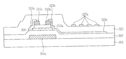
본 발명의 또 다른 실시 예에 따른 산화물 박막트랜지스터를 구비한 액정표시장치용 어레이기판은, 도 9에 도시된 바와 같이, 기판(301)상에 형성된 게이트전극(303a)과; 상기 게이트전극(303a)을 포함한 기판 전면에 형성된 게이트 절연막 (307)과; 상기 게이트전극(303a) 상측의 게이트 절연막(307) 상에 형성된 액티브층 (309)과; 상기 액티브층(309) 상에 형성된 식각정지층패턴(313a)과; 상기 식각정지층패턴(313a) 상에 형성되고 서로 이격된 소스부(315a) 및 드레인부(315b)와; 상기 소스부(315a)를 포함한 액티브층(309)과 접촉된 소스전극(323a)과, 상기 드레인부 (315b)을 포함한 액티브층(309)과 접촉된 드레인전극(323b)와; 상기 드레인전극 (323b)으로부터 연장된 대면적의 화소전극(323c)과; 상기 소스전극(323a) 및 드레인전극(323b)과 화소전극(323c)을 포함한 기판 전면에 형성된 패시베이션막(325)과; 상기 패시베이션막(325) 상부에 형성되고, 서로 이격되어 상기 화소전극(323c)과 대응하는 다수의 공통전극(327a)을 포함하여 구성된다.According to another exemplary embodiment of the present invention, an array substrate for an LCD device including an oxide thin film transistor may include: a
여기서, 상기 게이트전극(303a)은 실리콘, 유리, 플라스틱 또는 다른 적절한 물질을 포함하여 이루어지거나, 금속 또는 다른 적절한 도전 물질로 이루어질 수 있다. 예컨대, 상기 게이트전극(303a)으로는, 산화인듐주석(Indium Tin Oxide; ITO), 산화갈륨아연(Indium Gallium Zinc Oixde; GZO), 산화인듐갈륨아연(Indium Gallium Zinc Oxide; IGZO), 산화인듐갈륨(Indium Gallium Oixe; IGO), 산화인듐아연 (Indium Zinc Oxide; IZO), 산화인듐아연(Indium Zinc Oxide; IZO) 및 산화인듐 (In2O3)으로 이루어지는 그룹으로부터 선택되는 어느 하나 또는 이들의 2 이상의 조합 또는 다른 적절한 물질을 포함할 수도 있다. 또는 상기 게이트 전극(203a)의 형성 물질로는, 알루미늄(Al), 텅스텐(W), 구리 (Cu), 몰리브덴(Mo), 크롬(Cr), 티타늄 (Ti), 몰리텅스텐(MoW), 몰리티타늄 (MoTi), 구리/몰리티타늄 (Cu/MoTi)을 포함하는 도전성 금속 그룹 중에서 선택된 적어도 어느 하나 또는 이들의 2 이상의 조합 또는 다른 적절한 물질을 포함할 수도 있다. Here, the
또한, 상기 게이트 절연막(307)으로는 산화실리콘(SiO2), 질화실리콘(SiNx), 산화지르코늄(ZrO2), 산화하프늄(HfO2), 산화티타늄(TiO2), 산화탄탈륨(Ta2O5), 바륨-스트론튬-티타늄-산소화합물(Ba-Sr-Ti-O) 및 비스머스-아연-니오븀-산소 화합물(Bi-Zn-Nb-O)로 이루어지는 그룹으로부터 선택되는 어느 하나 또는 이들의 2 이상의 조합 또는 다른 적절한 물질을 포함할 수도 있다.In addition, the
그리고, 상기 액티브층(309)은 소스전극(323a)과 드레인전극(323b) 사이에 전자가 이동하는 채널을 형성하기 위한 층으로서, 저온 다결정 실리콘(Low Temperature Poly Silicon; 이하 LTPS라 함) 또는 비정질 실리콘(a-Si) 재질 대신에 실리콘(Si)을 포함하는 산화물 반도체로 이루어진다.The
이때, 상기 산화물 반도체로는, 게르마늄 (Ge), 주석(Sn), 납(Pb), 인듐 (In), 티타늄(Ti), 갈륨(Ga) 및 알루미늄(Al)으로 이루어지는 그룹으로부터 선택된 하나 이상의 물질 및 아연(Zn)을 포함하는 산화물 반도체에 실리콘 (Si)이 첨가된 물질로 이루어질 수 있다. 예컨대, 상기 액티브층(309)은 인듐아연 복합 산화물 (InZnO)에 실리콘 이온이 첨가된 실리콘 산화인듐아연(Si-InZnO: SIZO)으로 이루어질 수도 있다.In this case, the oxide semiconductor, at least one material selected from the group consisting of germanium (Ge), tin (Sn), lead (Pb), indium (In), titanium (Ti), gallium (Ga) and aluminum (Al). And silicon (Si) added to the oxide semiconductor including zinc (Zn). For example, the
상기 액티브층(309)이 SIZO로 이루어지는 경우, 액티브층에서 아연(Zn), 인듐(In) 및 실리콘(Si) 원자의 전체 함량 대비 실리콘(Si) 원자 함량의 조성비는 약 0.001 중량%(wt%) 내지 약 30 wt%일 수도 있다. 실리콘(Si) 원자 함량이 높아질수록 전자 생성을 제어하는 역할이 강해져서, 이동도가 낮아질 수 있으나, 그 소자의 안정성은 더 좋아질 수 있다.When the
한편, 상기 액티브층(309)으로는, 전술한 물질 외에 리튬(Li) 또는 칼륨(K)과 같은 I족 원소, 마그네슘(Mg), 칼슘(Ca) 또는 스트론튬(Sr)과 같은 Ⅱ족 원소, 갈륨(Ga), 알루미늄(Al), 인듐(In) 또는 이트륨(Y)과 같은 Ⅲ족 원소, 티타늄(Ti), 지르코늄(Zr), 실리콘(Si), 주석(Sn) 또는 게르마늄(Ge)과 같은 Ⅳ족 원소, 탄탈륨(Ta), 바나듐(V), 니오븀(Nb) 또는 안티몬(Sb)과 같은 Ⅴ족 원소, 또는 란티늄(La), 세륨(Ce), 프라세오디뮴(Pr), 네오디뮴(Nd), 프로메튬(Pm), 사마륨 (Sm), 유로퓸(Eu), 가돌리듐(Gd), 터븀(Tb), 디스프로슘(Dy), 홀뮴(Ho), 어븀(Er), 툴륨(Tm), 이터븀(Yb) 또는 루테듐(Lu)과 같은 란탄(Ln) 계열 원소 등이 더 포함될 수도 있다.On the other hand, the
또한, 상기 식각정지층패턴(313a)은 산화실리콘(SiO2)과 질화실리콘 (SiNx)으로 이루어진 무기 절연물질 중에서 어느 하나를 선택하여 사용한다.In addition, the etch
그리고, 상기 소스부(315a) 및 드레인부(315b)는 상기 게이트전극(203a)과 마찬가지로 금속 또는 다른 적절한 도전물질을 포함하여 이루어질 수 있다. 예컨대, 상기 소스부(315a) 및 드레인부(315b)는 산화인듐주석(Indium Tin Oxide; ITO), 산화갈륨아연(Indium Gallium Zinc Oixde; GZO), 산화인듐갈륨아연(Indium Gallium Zinc Oxide; IGZO), 산화인듐갈륨(Indium Gallium Oixe; IGO), 산화인듐아연 (Indium Zinc Oxide; IZO), 산화인듐아연(Indium Zinc Oxide; IZO) 및 산화인듐 (In2O3)으로 이루어지는 그룹으로부터 선택되는 어느 하나 또는 이들의 2 이상의 조합 또는 다른 적절한 물질을 포함할 수도 있다. 또는, 상기 소스부(315a) 및 드레인부(315b)는 알루미늄(Al), 텅스텐(W), 구리 (Cu), 몰리브덴(Mo), 크롬(Cr), 티타늄 (Ti), 몰리텅스텐(MoW), 몰리티타늄 (MoTi), 구리/몰리티타늄 (Cu/MoTi)을 포함하는 도전성 금속 그룹 중에서 선택된 적어도 어느 하나 또는 이들의 2 이상의 조합 또는 다른 적절한 물질을 포함할 수도 있다.The
특히, 상기 소스부(315a) 및 드레인부(315b)는 상기 식각정지층패턴(313a)의 영역 내에 한정하여 형성되며, 이들 소스부(315a) 및 드레인부(315b)는 상기 식각정지층패턴(313a) 영역 내에서 이격되어 형성된다. 이는 산화물 박막트랜지스터 제조시에, 하프톤 마스크를 이용한 마스크 공정시에, 상기 소스부(315a) 및 드레인부 (315b)가 상기 식각정지층패턴(313a)과 동일 마스크로 형성되기 때문에 가능하게 된다. In particular, the
따라서, 상기 소스부(315a) 및 드레인부(315b)와 오버랩되는 식각정지층패턴 (313a)의 일측 및 타측 간 제1 폭(W1)과 제2 폭(W2)은 항상 동일하게 유지됨으로써, 상기 소스부(315a) 및 드레인부(315b)과 식각정지층패턴(313a) 간의 오정렬(misalign)이 방지된다.Accordingly, the first width W1 and the second width W2 between one side and the other side of the etch
그리고, 상기 소스전극(323a) 및 드레인전극(323b)은 상기 드레인전극 (323b)으로부터 연장되어 대면적의 화소전극(323c)으로도 사용되어야 하기 때문에 투명한 도전 물질로 이루어지는데, 상기 투명한 도전 물질로는 ITO (Indium Tin Oxide), IZO(Indium Zinc Oxide)를 포함한 투명한 물질 그룹 중에서 선택된 어느 하나를 사용한다. Since the
또한, 상기 공통전극(327a)도 투명한 도전 물질로 이루어지는데, 상기 투명한 도전 물질로는 ITO (Indium Tin Oxide), IZO(Indium Zinc Oxide)를 포함한 투명한 물질 그룹 중에서 선택된 어느 하나를 사용한다. In addition, the
특히, 상기 소스전극(323a) 및 드레인전극(323b)은 각각 소스부(315a) 및 드레인부(315b) 상부를 포함한 상기 액티브층(309)의 노출된 부분과도 접촉되도록 형성됨으로써, 채널이 상기 소스전극(323a) 및 드레인전극(323b)와 연결되어 박막트랜지스터 특성이 나타나게 된다.In particular, the
이와 같은 구성으로 이루어지는 본 발명의 또 다른 실시 예에 따른 산화물 박막트랜지스터를 구비한 액정표시장치용 어레이기판 제조방법에 대해 첨부된 도면을 참조하여 상세히 설명한다.A method of manufacturing an array substrate for a liquid crystal display device having an oxide thin film transistor according to another embodiment of the present invention having such a configuration will be described in detail with reference to the accompanying drawings.
도 10a 내지 10k는 본 발명의 또 다른 실시 예에 따른 산화물 박막 트랜지스터를 구비한 액정표시장치용 어레이기판의 제조공정 단면도들이다.10A through 10K are cross-sectional views illustrating a process of manufacturing an array substrate for a liquid crystal display device having an oxide thin film transistor according to another exemplary embodiment of the present invention.
도 10a를 참조하면, 기판(301)상에 게이트전극용 제1 도전물질을 스퍼터링방법으로 증착하여 제1 도전층(303)을 형성하고, 그 위에 제1 감광막(미도시)을 도포한 후, 포토리소그라피 공정기술을 이용한 제1 마스크 공정을 통해 상기 제1 감광막(미도시)을 패터닝하여 제1 감광막패턴(305)을 형성한다.Referring to FIG. 10A, after depositing a first conductive material for a gate electrode on a
이때, 상기 제1 도전층(303)은 실리콘, 유리, 플라스틱 또는 다른 적절한 물질을 포함하여 이루어지거나, 금속 또는 다른 적절한 도전 물질로 이루어질 수 있다. 예컨대, 상기 게이트전극(303a)으로는, 산화인듐주석(Indium Tin Oxide; ITO), 산화갈륨아연(Indium Gallium Zinc Oixde; GZO), 산화인듐갈륨아연(Indium Gallium Zinc Oxide; IGZO), 산화인듐갈륨(Indium Gallium Oixe; IGO), 산화인듐아연 (Indium Zinc Oxide; IZO), 산화인듐아연(Indium Zinc Oxide; IZO) 및 산화인듐 (In2O3)으로 이루어지는 그룹으로부터 선택되는 어느 하나 또는 이들의 2 이상의 조합 또는 다른 적절한 물질을 포함할 수도 있다. 또는 상기 제1 도전층(203)의 형성 물질로는, 알루미늄(Al), 텅스텐(W), 구리 (Cu), 몰리브덴(Mo), 크롬(Cr), 티타늄 (Ti), 몰리텅스텐(MoW), 몰리티타늄 (MoTi), 구리/몰리티타늄 (Cu/MoTi)을 포함하는 도전성 금속 그룹 중에서 선택된 적어도 어느 하나 또는 이들의 2 이상의 조합 또는 다른 적절한 물질을 포함할 수도 있다. In this case, the first
그 다음, 도 10b를 참조하면, 상기 제1 감광막패턴(305)을 식각 마스크로 상기 제1 도전층(303)을 선택적으로 식각하여 게이트전극(303a)을 형성한다. Next, referring to FIG. 10B, the first
이어서, 도 10c를 참조하면, 상기 제1 감광막패턴(305)을 제거하고, 상기 게이트전극(303a)을 포함한 기판 전면에 게이트 절연막(307)을 형성한다. 이때, 상기 게이트 절연막(307)으로는 산화실리콘(SiO2), 질화실리콘(SiNx), 산화지르코늄 (ZrO2), 산화하프늄(HfO2), 산화티타늄(TiO2), 산화탄탈륨(Ta2O5), 바륨-스트론튬-티타늄-산소화합물(Ba-Sr-Ti-O) 및 비스머스-아연-니오븀-산소 화합물(Bi-Zn-Nb-O)로 이루어지는 그룹으로부터 선택되는 어느 하나 또는 이들의 2 이상의 조합 또는 다른 적절한 물질을 포함할 수도 있다.Next, referring to FIG. 10C, the first
이어서, 상기 게이트 절연막(307) 상에 산화물 반도체 물질을 이용하여 반도체층(미도시)을 형성하고, 그 위에 제2 감광막(미도시)을 도포한다. Subsequently, a semiconductor layer (not shown) is formed on the
그 다음, 도면에는 도시하지 않았지만, 포토리소그라피 공정기술을 이용한 제2 마스크 공정을 통해 상기 제2 감광막(미도시)을 패터닝하여 제2 감광막패턴 (미도시)을 형성한다.Next, although not shown in the drawing, the second photoresist film (not shown) is patterned through a second mask process using a photolithography process technology to form a second photoresist pattern (not shown).
이어서, 도 10c를 참조하면, 상기 제2 감광막패턴(미도시)을 식각 마스크로 상기 반도체층(미도시)을 선택적으로 제거하여, 상기 게이트전극(303a) 상측의 게이트 절연막(307) 상에 액티브층(309)을 형성한다. 이때, 상기 액티브층(309)은 소스전극(미도시)과 드레인전극(미도시) 사이에 전자가 이동하는 채널을 형성하기 위한 층으로서, 저온 다결정 실리콘(Low Temperature Poly Silicon; 이하 LTPS라 함) 또는 비정질 실리콘(a-Si) 재질 대신에 실리콘(Si)을 포함하는 산화물 반도체로 이루어진다.Subsequently, referring to FIG. 10C, the semiconductor layer (not shown) is selectively removed using the second photoresist pattern (not shown) as an etch mask to be active on the
이때, 상기 산화물 반도체로는, 게르마늄 (Ge), 주석(Sn), 납(Pb), 인듐 (In), 티타늄(Ti), 갈륨(Ga) 및 알루미늄(Al)으로 이루어지는 그룹으로부터 선택된 하나 이상의 물질 및 아연(Zn)을 포함하는 산화물 반도체에 실리콘 (Si)이 첨가된 물질로 이루어질 수 있다. 예컨대, 상기 액티브패턴(109a)은 인듐아연 복합 산화물(InZnO)에 실리콘 이온이 첨가된 실리콘 산화인듐아연(Si-InZnO: SIZO)으로 이루어질 수도 있다.In this case, the oxide semiconductor, at least one material selected from the group consisting of germanium (Ge), tin (Sn), lead (Pb), indium (In), titanium (Ti), gallium (Ga) and aluminum (Al). And silicon (Si) added to the oxide semiconductor including zinc (Zn). For example, the active pattern 109a may be formed of silicon indium zinc oxide (Si-InZnO: SIZO) in which silicon ions are added to indium zinc complex oxide (InZnO).
상기 액티브층(309)이 SIZO로 이루어지는 경우, 액티브층에서 아연(Zn), 인듐(In) 및 실리콘(Si) 원자의 전체 함량 대비 실리콘(Si) 원자 함량의 조성비는 약 0.001 중량%(wt%) 내지 약 30 wt%일 수도 있다. 실리콘(Si) 원자 함량이 높아질수록 전자 생성을 제어하는 역할이 강해져서, 이동도가 낮아질 수 있으나, 그 소자의 안정성은 더 좋아질 수 있다.When the
한편, 상기 액티브층(309)으로는, 전술한 물질 외에 리튬(Li) 또는 칼륨(K)과 같은 I족 원소, 마그네슘(Mg), 칼슘(Ca) 또는 스트론튬(Sr)과 같은 Ⅱ족 원소, 갈륨(Ga), 알루미늄(Al), 인듐(In) 또는 이트륨(Y)과 같은 Ⅲ족 원소, 티타늄(Ti), 지르코늄(Zr), 실리콘(Si), 주석(Sn) 또는 게르마늄(Ge)과 같은 Ⅳ족 원소, 탄탈륨(Ta), 바나듐(V), 니오븀(Nb) 또는 안티몬(Sb)과 같은 Ⅴ족 원소, 또는 란티늄(La), 세륨(Ce), 프라세오디뮴(Pr), 네오디뮴(Nd), 프로메튬(Pm), 사마륨 (Sm), 유로퓸(Eu), 가돌리듐(Gd), 터븀(Tb), 디스프로슘(Dy), 홀뮴(Ho), 어븀(Er), 툴륨(Tm), 이터븀(Yb) 또는 루테듐(Lu)과 같은 란탄(Ln) 계열 원소 등이 더 포함될 수도 있다.On the other hand, the
그 다음, 도 10d를 참조하면, 상기 액티브층(209)을 포함한 기판 전면에 식각정지층(313)과 제2 도전층(315)을 차례로 적층하고, 그 위에 다시 제3 감광막 (317)을 도포한다. 이때, 상기 식각정지층(313)은 산화실리콘(SiO2)과 질화실리콘 (SiNx)으로 이루어진 무기 절연물질 중에서 어느 하나를 선택하여 사용한다.Next, referring to FIG. 10D, the
또한, 상기 제2 도전층(315)은 상기 게이트전극(303a)과 마찬가지로 금속 또는 다른 적절한 도전물질을 포함하여 이루어질 수 있다. 예컨대, 상기 제2 도전층 (117)은 산화인듐주석(Indium Tin Oxide; ITO), 산화갈륨아연(Indium Gallium Zinc Oixde; GZO), 산화인듐갈륨아연(Indium Gallium Zinc Oxide; IGZO), 산화인듐갈륨 (Indium Gallium Oixe; IGO), 산화인듐아연 (Indium Zinc Oxide; IZO), 산화인듐아연(Indium Zinc Oxide; IZO) 및 산화인듐 (In2O3)으로 이루어지는 그룹으로부터 선택되는 어느 하나 또는 이들의 2 이상의 조합 또는 다른 적절한 물질을 포함할 수도 있다. 또는, 상기 제2 도전층(315)은 알루미늄(Al), 텅스텐(W), 구리 (Cu), 몰리브덴(Mo), 크롬(Cr), 티타늄 (Ti), 몰리텅스텐(MoW), 몰리티타늄 (MoTi), 구리/몰리티타늄 (Cu/MoTi)을 포함하는 도전성 금속 그룹 중에서 선택된 적어도 어느 하나 또는 이들의 2 이상의 조합 또는 다른 적절한 물질을 포함할 수도 있다.In addition, like the
이어서, 하프톤 마스크(Half-Ton Mask)(321)를 이용한 포토리소그라피 공정기술을 통해 노광 공정을 실시한다. 이때, 상기 하프톤 마스크(321)는 제1 광차단패턴(321a)과 제2 광차단패턴(321b)을 포함하고 있는데, 상기 제1 광차단패턴 (321a)은 광을 전부 차단하는 역할을 담당하고, 상기 제2 광차단패턴(321b)은 광의 일부는 투과시키고, 나머지는 차단하는 역할을 담당한다.Subsequently, an exposure process is performed through a photolithography process technology using a half-
그 다음, 도 10e를 참조하면, 상기 노광 공정을 통해 광이 투과된 제3 감광막 (317) 부분을 현상 공정을 통해 제거하여, 두께가 다른 제3 감광막패턴(317a, 317b)을 형성한다. 이때, 두께가 얇은 제3 감광막패턴(317b)은 상기 액티브층 (309)의 채널영역 상부에 위치하며, 두께가 두꺼운 제3 감광막패턴(317a)은 후속 공정에서 형성될 소스부 및 드레인부 상부에 위치하게 된다.Next, referring to FIG. 10E, a portion of the third
이어서, 도 10f에 도시된 바와 같이, 상기 제3 감광막패턴(317a, 317b)을 식각 마스크로 상기 제2 도전층(315)과 식각정지층(313)을 선택적으로 식각하여 식각정지층패턴(313a)을 형성한다. 이때, 상기 식각정지층패턴(313a)은 상기 액티브층 (309) 보다 면적이 작으며, 상기 액티브층(309)의 일부는 외부로 노출된 상태가 된다.Subsequently, as illustrated in FIG. 10F, the second
그 다음, 도 10g를 참조하면, 상기 제3 감광막패턴(317a, 317b) 중에서, 상기 제3 감광막패턴(317b)이 완전 제거될 때까지 에싱(Ashing) 공정을 실시한다. 이때, 상기 제3 감광막패턴(317a) 일부도 함께 제거된다. 또한, 상기 제3 감광막패턴 (317b)이 완전 제거됨으로 인해, 그 하부의 제2 도전층(315) 부분이 외부로 노출된다.Next, referring to FIG. 10G, an ashing process may be performed until the
이어서, 도 10h를 참조하면, 상기 제3 감광막패턴(317a)을 식각 마스크로 상기 제2 도전층(315)의 노출된 부분을 식각하여, 서로 이격된 소스부(315a) 및 드레인부(315b)를 형성한다. 이때, 상기 소스부(315a) 및 드레인부(315b)는 상기 식각정지층패턴(313a)의 영역 내에 한정하여 형성되며, 이들 소스부(315a) 및 드레인부 (315b)는 상기 식각정지층패턴(313a) 영역 내에서 이격되어 형성된다. 이는 산화물 박막트랜지스터 제조시에, 하프톤 마스크를 이용한 마스크 공정시에, 상기 소스부 (315a) 및 드레인부(315b)가 상기 식각정지층패턴(313a)과 동일 마스크로 형성되기 때문에 가능하게 된다. 이때, 상기 소스부(315a) 및 드레인부(315b) 형성시에, 데이터배선 (미도시)도 함께 형성된다.Subsequently, referring to FIG. 10H, exposed portions of the second
따라서, 상기 소스부(315a) 및 드레인부(315b)와 오버랩되는 식각정지층패턴 (313a)의 일측 및 타측 간 제1 폭(W1)과 제2 폭(W2)은 항상 동일하게 유지됨으로 써, 상기 소스부(315a) 및 드레인부(315b)과 식각정지층패턴(313a) 간의 오정렬 (misalign)이 방지된다.Therefore, the first width W1 and the second width W2 between one side and the other side of the etch
그 다음, 상기 소스부(315a) 및 드레인부(315b)를 포함한 기판 전면에, 제3 도전층(323)을 증착하고, 그 위에 제4 감광막(미도시)을 도포한다. 이때, 상기 제3 도전층(323)은 드레인전극으로부터 연장되어 대면적의 화소전극으로도 사용되어야 하기 때문에 투명한 도전 물질로 이루어지는데, 상기 투명한 도전 물질로는 ITO (Indium Tin Oxide), IZO(Indium Zinc Oxide)를 포함한 투명한 물질 그룹 중에서 선택된 어느 하나를 사용한다. Next, a third
이어서, 도면에는 도시하지 않았지만, 포토리소그라피 공정기술을 이용한 제4 마스크 공정을 통해 상기 제4 감광막(미도시)을 선택적으로 패터닝하여, 제4 감광막패턴(미도시)을 형성한다. Next, although not shown in the drawing, the fourth photoresist layer (not shown) is selectively patterned through a fourth mask process using a photolithography process technology to form a fourth photoresist layer pattern (not shown).
그 다음, 도 10i를 참조하면, 상기 제4 감광막패턴(미도시)을 식각마스크로 상기 제3 도전층(323)을 선택적으로 식각하여, 소스전극(323a)과 드레인전극(323b)과 함께 이 드레인전극(323b)으로부터 연장된 대면적의 화소전극(323c)을 동시에 형성한다. 이때, 상기 소스전극(323a) 및 드레인전극(323b)은 각각 소스부(315a) 및 드레인부(315b) 상부를 포함한 상기 액티브층(309)의 노출된 부분과도 접촉되도록 형성됨으로써, 채널이 상기 소스전극(323a) 및 드레인전극(323b)과 연결되어 박막트랜지스터 특성이 나타나게 된다.Next, referring to FIG. 10I, the third
이어서, 도 10j를 참조하면, 상기 소스전극(323a)과 드레인전극(323b) 및 화소전극(323c)을 포함한 기판 전면에 패시베이션막(325)을 증착한다. 이때, 상기 패시베이션막(325)으로는 질화막 및 산화막을 포함하는 무기절연물질 또는 유기절연물질 중에서 어느 하나를 선택하여 사용할 수 있다.Next, referring to FIG. 10J, a
그 다음, 상기 패시베이션막(325) 상부에 제4 도전층(327)을 스퍼터링 방법으로 증착하고, 그 위에 제5 감광막(미도시)을 도포한다. 이때, 상기 제4 도전층 (327)으로는, 투명한 도전 물질을 사용하는데, 상기 투명한 도전 물질로는 ITO (Indium Tin Oxide), IZO(Indium Zinc Oxide)를 포함한 투명한 물질 그룹 중에서 선택된 어느 하나를 사용한다. Next, a fourth
이어서, 도면에는 도시하지 않았지만, 포토리소그라피 공정기술을 이용한 제5 마스크 공정을 통해 상기 제5 감광막(미도시)을 패터닝하여, 제5 감광막패턴 (미도시)을 형성한다.Subsequently, although not shown in the drawing, the fifth photoresist film (not shown) is patterned through a fifth mask process using a photolithography process technology to form a fifth photoresist pattern (not shown).
이어서, 도 10k를 참조하면, 상기 제5 감광막패턴(미도시)을 식각마스크로, 상기 제4 도전층(327)을 선택적으로 식각하여, 상기 화소전극(323c)와 대응하는 다수의 분기된 공통전극(327a)을 형성함으로써, 본 발명의 또 다른 실시 예에 따른 산화물 박막트랜지스터를 구비한 액정표시장치용 어레이기판 제조공정을 완료한다. Subsequently, referring to FIG. 10K, the fourth photoresist layer pattern (not shown) is etched and the fourth
이상에서와 같이, 본 발명에 따르면, 소스부 및 드레인부 또는 데이터배선 형성시에 하프톤 마스크(half-ton mask)를 적용하여 소스부 및 드레인부 또는 데이터배선과 식각정지층을 형성할 수 있어, 소스부 및 드레인부와 식각정지층이 오정렬되는 현상이 제거된다.As described above, according to the present invention, the source and drain portions or the data wiring and the etch stop layer may be formed by applying a half-tone mask when the source and drain portions or the data wiring are formed. The misalignment of the source and drain portions with the etch stop layer is eliminated.
또한, 본 발명에 따르면, 소스부 및 드레인부와 식각 정지층을 하프톤 마스크를 적용하여 형성할 수 있기 때문에, 소스부 및 드레인부와 식각정지층 간의 정렬 마진(align margin)이 감소함에 따라 단채널(short channel) 구현이 가능하게 된다.In addition, according to the present invention, since the source and drain portions and the etch stop layer may be formed by applying a halftone mask, as the alignment margin between the source and drain portions and the etch stop layer decreases, Short channel implementations are possible.
그리고, 본 발명에 따르면, 소스부 및 드레인부 또는 데이터배선 형성시에 하프톤 마스크(half-ton mask)를 적용하여 소스부 및 드레인부 또는 데이터배선과 식각정지층을 형성할 수 있어 포토 오정렬(photo misalign)이 제거됨에 따라, 공정 변동에 따른 소자 특성 차 및 기판 내의 소자 균일성 (uniformity) 특성이 향상된다. In addition, according to the present invention, a half-ton mask may be applied when the source and drain portions or the data lines are formed to form the source and drain portions or the data lines and the etch stop layer. As photo misalignment is eliminated, device characteristic differences due to process variations and device uniformity characteristics in the substrate are improved.
더욱이, 본 발명에 따르면, 소스부 및 드레인부와 식각 정지층을 하프톤 마스크를 적용하여 형성할 수 있기 때문에 마스크 수가 저감되어 제조 비용이 절감되는 효과가 있다.Furthermore, according to the present invention, since the source portion, the drain portion, and the etch stop layer can be formed by applying a halftone mask, the number of masks is reduced, thereby reducing the manufacturing cost.
따라서, 본 발명에 따른 산화물 박막트랜지스터를 구비한 액정표시장치용 어레이기판 및 그 제조방법은, 액티브층 이 실리콘을 포함하는 산화물 반도체로 이루어지므로 높은 전자 이동도를 가지며, 생산 단가가 낮은 이점이 있다. 또한, 상기 액티브층의 제조 공정은 상온에서도 수행 가능하므로 공정을 용이하게 할 수 있다.Accordingly, an array substrate for a liquid crystal display device having an oxide thin film transistor and a method of manufacturing the same according to the present invention have an advantage of high electron mobility and low production cost since the active layer is made of an oxide semiconductor containing silicon. . In addition, the manufacturing process of the active layer may be performed at room temperature, thereby facilitating the process.
한편, 본 발명에 따른 산화물 박막 트랜지스터는 기존의 비정질 실리콘 박막트랜지스터(a-Si TFT)나 다결정 실리콘 박막트랜지스터(poly-Si TFT)를 대체할 수 있는 산화물 반도체 박막트랜지스터(oxide TFT) 소자 제작에 응용될 수 있다.Meanwhile, the oxide thin film transistor according to the present invention is applied to fabrication of an oxide semiconductor thin film transistor (oxide TFT) device that can replace an existing amorphous silicon thin film transistor (a-Si TFT) or polycrystalline silicon thin film transistor (poly-Si TFT). Can be.
또한, 상기 박막트랜지스터를 기반으로 한 스위칭 및 구동 소자가 요구되는 평판디스플레이, 특히 액정디스플레이(LCD)와 유기발광디스플레이(OLED)에 적용될 수 있다. In addition, the switching and driving device based on the thin film transistor may be applied to a flat panel display, in particular, a liquid crystal display (LCD) and an organic light emitting display (OLED).
최종적으로 액정디스플레이(LCD) 또는 유기발광디스플레이(OLED)를 채용한 평판디스플레이 제품, 핸드폰 및 모바일기기, 노트북, 모니터, TV제품에 적용된다.Finally, it is applied to flat panel display products, cell phones and mobile devices, laptops, monitors, and TV products employing liquid crystal display (LCD) or organic light emitting display (OLED).
상기한 설명에서 많은 사항이 구체적으로 기재되어 있으나, 그들은 발명의 범위를 한정하는 것이라기보다, 바람직한 실시 예의 예시로서 해석되어야 한다. 예를 들어, 본 발명이 속하는 기술 분야에서 통상의 지식을 가진 자라면, 본 발명의 박막트랜지스터의 구성 요소는 다양화할 수 있을 것이고, 구조 또한 다양한 형태로 변형할 수 있을 것이다. While many details are set forth in the foregoing description, they should be construed as illustrative of preferred embodiments, rather than to limit the scope of the invention. For example, those of ordinary skill in the art to which the present invention pertains will be able to vary the components of the thin film transistor of the present invention, the structure may also be modified in various forms.
또한, 본 발명의 산화물 박막 트랜지스터는 액정표시장치나 유기발광표시장치뿐만 아니라 메모리소자 및 논리 소자 분야에도 적용될 수 있음을 알 수 있을 것이다. 때문에 본 발명의 범위는 설명된 실시 예에 의하여 정하여 질 것이 아니고 특허 청구범위에 기재된 기술적 사상에 의해 정하여져야 한다.In addition, it will be appreciated that the oxide thin film transistor of the present invention can be applied not only to a liquid crystal display device or an organic light emitting display device but also to a memory device and a logic device field. Therefore, the scope of the present invention should not be defined by the described embodiments, but should be determined by the technical spirit described in the claims.
100: 산화물 박막트랜지스터 103a: 게이트전극
107: 게이트 절연막 109: 액티브층
113a: 식각정지층패턴 115a: 소스부
115b: 드레인부 121: 하프톤 마스크
121a: 제1 광차단패턴 121b: 제2 광차단패턴
123a: 소스전극 123b: 드레인전극100: oxide
107: gate insulating film 109: active layer
113a: etch
115b: drain 121: halftone mask
121a: first
123a:
Claims (20)
상기 게이트전극을 포함한 기판 전면에 형성된 게이트 절연막;
상기 게이트전극 상측의 게이트 절연막 상에 산화물 반도체로 형성된 액티브층;
상기 액티브층 상에 형성된 식각정지층패턴과;
상기 식각정지층패턴 상내에 서로 이격되어 형성되는 소스부 및 드레인부;
상기 소스부 및 드레인부를 포함한 기판 전면에 형성되고, 상기 액티브층을 노출시키는 소스전극 콘택홀과 드레인전극 콘택홀을 구비한 패시베이션막;
상기 패시베이션막 상부에 형성되고, 상기 소스전극 콘택홀을 통해 상기 소스부와 상기 액티브층에 접촉된 소스전극과, 상기 드레인전극 콘택홀을 통해 상기 드레인부와 상기 액티브층에 접촉된 드레인전극; 및
상기 패시베이션막 상에 형성되고, 상기 드레인전극으로부터 연장된 다수의 분기된 화소전극과 이 화소전극과 이격된 다수의 분기된 공통전극;을 포함하여 구성되는 산화물 박막트랜지스터를 구비하고,
상기 소스부와 상기 식각정지층패턴간의 오버랩되는 채널 길이 방향의 폭은 상기 드레인부와 상기 식각정지층패턴 간의 오버랩되는 채널 길이 방향의 폭과 동일한 것을 특징으로 하는 산화물 박막트랜지스터를 구비한 표시장치용 어레이기판.A gate electrode formed on the substrate;
A gate insulating film formed on an entire surface of the substrate including the gate electrode;
An active layer formed of an oxide semiconductor on the gate insulating layer above the gate electrode;
An etch stop layer pattern formed on the active layer;
Source and drain portions formed on the etch stop layer pattern and spaced apart from each other;
A passivation film formed over the substrate including the source and drain portions and having a source electrode contact hole and a drain electrode contact hole exposing the active layer;
A source electrode formed on the passivation layer, the source electrode contacting the source portion and the active layer through the source electrode contact hole, and the drain electrode contacting the drain portion and the active layer through the drain electrode contact hole; And
An oxide thin film transistor formed on the passivation layer, the plurality of branched pixel electrodes extending from the drain electrode and the plurality of branched common electrodes spaced apart from the pixel electrode;
The width of the overlapping channel length direction between the source portion and the etch stop layer pattern is the same as the width of the overlapping channel length direction between the drain portion and the etch stop layer pattern for a display device having an oxide thin film transistor Array substrate.
상기 게이트전극을 포함한 기판 전면에 게이트 절연막을 형성하는 단계;
상기 게이트전극 상측의 게이트 절연막 상에 산화물 반도체로 이루어진 액티브층을 형성하는 단계;
상기 액티브층을 포함한 기판 전면에 식각정지층과 도전층을 차례로 적층하는 단계;
상기 도전층상에 감광막을 도포하고 하프톤 마스크를 이용한 노광 및 현상 공정으로 두께가 다른 감광막 패턴을 형성하는 단계;
상기 감광막 패턴을 마스크로 상기 도전층과 식각정지층을 선택적으로 식각하여 도전층패턴과 식각정지층패턴을 형성하는 단계;
상기 감광막 패턴을 애싱 처리하고 잔류한 감광막 패턴을 마스크로 상기 도전층패턴을 선택적으로 식각하여 상기 식각정지층패턴 상내에 소스부 및 드레인부를 형성하는 단계;
상기 감광막 패턴을 제거하고 상기 소스부 및 드레인부를 포함한 기판 전면에 상기 액티브층을 노출시키는 소스전극 콘택홀과 드레인전극 콘택홀을 구비한 패시베이션막을 형성하는 단계; 및
상기 소스전극 콘택홀을 통해 상기 소스부와 상기 액티브층에 접촉된 소스전극과, 상기 드레인전극 콘택홀을 통해 상기 드레인부와 상기 액티브층에 접촉된 드레인전극과 함께 이 드레인전극으로부터 연장된 다수의 분기된 화소전극 및 상기 드레인전극으로부터 연장된 다수의 분기된 화소전극과 서로 이격된 다수의 공통전극을 형성하는 단계;를 포함하여 구성되는 산화물 박막트랜지스터를 구비한 표시장치용 어레이기판 제조방법. Forming a gate electrode on the substrate;
Forming a gate insulating film on an entire surface of the substrate including the gate electrode;
Forming an active layer made of an oxide semiconductor on the gate insulating film above the gate electrode;
Sequentially stacking an etch stop layer and a conductive layer on the entire surface of the substrate including the active layer;
Forming a photosensitive film pattern having a different thickness by applying a photosensitive film on the conductive layer and exposing and developing a halftone mask;
Selectively etching the conductive layer and the etch stop layer using the photoresist pattern as a mask to form a conductive layer pattern and an etch stop layer pattern;
Ashing the photoresist pattern and selectively etching the conductive layer pattern using the remaining photoresist pattern to form a source portion and a drain portion on the etch stop layer pattern;
Removing the photoresist pattern and forming a passivation layer including a source electrode contact hole and a drain electrode contact hole exposing the active layer on the entire surface of the substrate including the source and drain portions; And
A plurality of source electrodes contacting the source portion and the active layer through the source electrode contact hole and drain electrodes contacting the drain portion and the active layer through the drain electrode contact hole; And forming a plurality of branched pixel electrodes and a plurality of branched pixel electrodes extending from the drain electrode and a plurality of common electrodes spaced apart from each other. 2. A method of manufacturing an array substrate for a display device, comprising: an oxide thin film transistor;
Priority Applications (3)
| Application Number | Priority Date | Filing Date | Title |
|---|---|---|---|
| KR1020120055683A KR102023924B1 (en) | 2012-05-24 | 2012-05-24 | Oxide thin film transistor having array substrate for display device and method for fabricating the same |
| US13/728,732 US8921850B2 (en) | 2012-05-24 | 2012-12-27 | Oxide thin film transistor, method for fabricating TFT, array substrate for display device and method for fabricating the same |
| CN201210586802.6A CN103426934B (en) | 2012-05-24 | 2012-12-28 | Oxide thin film transistor and manufacture method thereof, array base palte and manufacture method thereof |
Applications Claiming Priority (1)
| Application Number | Priority Date | Filing Date | Title |
|---|---|---|---|
| KR1020120055683A KR102023924B1 (en) | 2012-05-24 | 2012-05-24 | Oxide thin film transistor having array substrate for display device and method for fabricating the same |
Publications (2)
| Publication Number | Publication Date |
|---|---|
| KR20130131823A KR20130131823A (en) | 2013-12-04 |
| KR102023924B1 true KR102023924B1 (en) | 2019-09-23 |
Family
ID=49620895
Family Applications (1)
| Application Number | Title | Priority Date | Filing Date |
|---|---|---|---|
| KR1020120055683A Active KR102023924B1 (en) | 2012-05-24 | 2012-05-24 | Oxide thin film transistor having array substrate for display device and method for fabricating the same |
Country Status (3)
| Country | Link |
|---|---|
| US (1) | US8921850B2 (en) |
| KR (1) | KR102023924B1 (en) |
| CN (1) | CN103426934B (en) |
Cited By (2)
| Publication number | Priority date | Publication date | Assignee | Title |
|---|---|---|---|---|
| KR20210152083A (en) | 2020-06-05 | 2021-12-15 | 삼성디스플레이 주식회사 | Display device |
| US11626471B2 (en) | 2020-09-14 | 2023-04-11 | Samsung Display Co., Ltd. | Display device including transistor with separate insulating patterns and etch stoppers overlying active layer thereof, and method of manufacturing the same |
Families Citing this family (26)
| Publication number | Priority date | Publication date | Assignee | Title |
|---|---|---|---|---|
| CN102651401B (en) * | 2011-12-31 | 2015-03-18 | 京东方科技集团股份有限公司 | A kind of thin film transistor, array substrate and its manufacturing method and display device |
| TWI520221B (en) * | 2013-07-25 | 2016-02-01 | 中華映管股份有限公司 | Thin film transistor and method of manufacturing same |
| US9082664B2 (en) * | 2013-11-12 | 2015-07-14 | Shenzhen China Star Optoelectronics Technology Co., Ltd | Method for manufacturing thin-film transistor substrate and thin-film transistor substrate manufactured with same |
| HK1251495A1 (en) | 2015-06-26 | 2019-02-01 | 科耐立制造公司 | Method of providing doses of light sufficient to deactivate dangerous pathogens throughout a volumetric space over a period of time |
| US10363325B2 (en) | 2015-06-26 | 2019-07-30 | Kenall Manufacturing Company | Lighting device that deactivates dangerous pathogens while providing visually appealing light |
| US11273324B2 (en) | 2015-07-14 | 2022-03-15 | Illumipure Corp | LED structure and luminaire for continuous disinfection |
| JP2018525848A (en) | 2015-07-30 | 2018-09-06 | バイタル バイオ、 インコーポレイテッド | Single diode sterilization |
| US10918747B2 (en) | 2015-07-30 | 2021-02-16 | Vital Vio, Inc. | Disinfecting lighting device |
| US10357582B1 (en) | 2015-07-30 | 2019-07-23 | Vital Vio, Inc. | Disinfecting lighting device |
| CN105161519B (en) | 2015-08-20 | 2018-03-27 | 京东方科技集团股份有限公司 | Thin film transistor (TFT) and preparation method, array base palte and preparation method and display device |
| US10942409B2 (en) * | 2016-09-01 | 2021-03-09 | Sharp Kabushiki Kaisha | Active-matrix substrate and display device |
| US10006619B1 (en) | 2016-12-28 | 2018-06-26 | WLC Enterprises, Inc. | Combination LED lighting and fan apparatus |
| US20180185533A1 (en) | 2016-12-29 | 2018-07-05 | Vital Vio, Inc. | Control systems for disinfecting light systems and methods of regulating operations of disinfecting light systems |
| US10835627B2 (en) | 2017-12-01 | 2020-11-17 | Vital Vio, Inc. | Devices using flexible light emitting layer for creating disinfecting illuminated surface, and related method |
| US10309614B1 (en) | 2017-12-05 | 2019-06-04 | Vital Vivo, Inc. | Light directing element |
| US10413626B1 (en) | 2018-03-29 | 2019-09-17 | Vital Vio, Inc. | Multiple light emitter for inactivating microorganisms |
| CN109659313B (en) * | 2018-11-12 | 2021-04-02 | 惠科股份有限公司 | Array substrate, manufacturing method of array substrate, and display panel |
| US12194168B2 (en) | 2018-12-19 | 2025-01-14 | Vyv, Inc. | Lighting and dissipation device |
| US11639897B2 (en) | 2019-03-29 | 2023-05-02 | Vyv, Inc. | Contamination load sensing device |
| US11541135B2 (en) | 2019-06-28 | 2023-01-03 | Vyv, Inc. | Multiple band visible light disinfection |
| US11369704B2 (en) | 2019-08-15 | 2022-06-28 | Vyv, Inc. | Devices configured to disinfect interiors |
| US11878084B2 (en) | 2019-09-20 | 2024-01-23 | Vyv, Inc. | Disinfecting light emitting subcomponent |
| US11499707B2 (en) | 2020-04-13 | 2022-11-15 | Calyxpure, Inc. | Light fixture having a fan and ultraviolet sterilization functionality |
| US11759540B2 (en) | 2021-05-11 | 2023-09-19 | Calyxpure, Inc. | Portable disinfection unit |
| US20220362432A1 (en) | 2021-05-11 | 2022-11-17 | Calyxpure, Inc. | Sensor System for a Light Fixture Having Ultraviolet Sterilization Functionality |
| JP2023054475A (en) * | 2021-10-04 | 2023-04-14 | 株式会社ジャパンディスプレイ | Semiconductor device and manufacturing method for the same |
Citations (1)
| Publication number | Priority date | Publication date | Assignee | Title |
|---|---|---|---|---|
| JP2009192932A (en) * | 2008-02-15 | 2009-08-27 | Mitsubishi Electric Corp | Liquid crystal display device and manufacturing method thereof |
Family Cites Families (13)
| Publication number | Priority date | Publication date | Assignee | Title |
|---|---|---|---|---|
| US6025605A (en) * | 1996-07-26 | 2000-02-15 | Lg Electronics Inc. | Aligned semiconductor structure |
| JPH11274505A (en) * | 1998-03-23 | 1999-10-08 | Nec Corp | Thin film transistor structure and its manufacture |
| US6049365A (en) * | 1998-05-07 | 2000-04-11 | Mitsubishi Denki Kabushiki Kaisha | Liquid crystal displaying apparatus with a converter not exposed to liquid crystal |
| US6218221B1 (en) * | 1999-05-27 | 2001-04-17 | Chi Mei Optoelectronics Corp. | Thin film transistor with a multi-metal structure and a method of manufacturing the same |
| US6774397B2 (en) * | 2000-05-12 | 2004-08-10 | Semiconductor Energy Laboratory Co., Ltd. | Semiconductor device |
| KR100516508B1 (en) * | 2002-05-06 | 2005-09-22 | 진 장 | Thin film transistor plat and fabrication method thereof |
| KR100936908B1 (en) * | 2003-07-18 | 2010-01-18 | 삼성전자주식회사 | Thin film transistor of electroluminescent device, electroluminescent device using same and manufacturing method thereof |
| KR101282893B1 (en) * | 2006-06-30 | 2013-07-05 | 엘지디스플레이 주식회사 | An array substrate for LCD and method for fabricating thereof |
| US8227278B2 (en) * | 2008-09-05 | 2012-07-24 | Semiconductor Energy Laboratory Co., Ltd. | Methods for manufacturing thin film transistor and display device |
| KR101019048B1 (en) * | 2008-11-20 | 2011-03-07 | 엘지디스플레이 주식회사 | Array substrate and its manufacturing method |
| JP2012069540A (en) * | 2010-09-21 | 2012-04-05 | Casio Comput Co Ltd | Thin film transistor, manufacturing method for thin film transistor, and light-emitting device |
| KR101774478B1 (en) * | 2010-10-22 | 2017-09-05 | 삼성디스플레이 주식회사 | Thin film transistor and manufacturing method thereof |
| KR20120042064A (en) * | 2010-10-22 | 2012-05-03 | 삼성모바일디스플레이주식회사 | Thin film transistor |
-
2012
- 2012-05-24 KR KR1020120055683A patent/KR102023924B1/en active Active
- 2012-12-27 US US13/728,732 patent/US8921850B2/en active Active
- 2012-12-28 CN CN201210586802.6A patent/CN103426934B/en active Active
Patent Citations (1)
| Publication number | Priority date | Publication date | Assignee | Title |
|---|---|---|---|---|
| JP2009192932A (en) * | 2008-02-15 | 2009-08-27 | Mitsubishi Electric Corp | Liquid crystal display device and manufacturing method thereof |
Cited By (3)
| Publication number | Priority date | Publication date | Assignee | Title |
|---|---|---|---|---|
| KR20210152083A (en) | 2020-06-05 | 2021-12-15 | 삼성디스플레이 주식회사 | Display device |
| US11626471B2 (en) | 2020-09-14 | 2023-04-11 | Samsung Display Co., Ltd. | Display device including transistor with separate insulating patterns and etch stoppers overlying active layer thereof, and method of manufacturing the same |
| US11917878B2 (en) | 2020-09-14 | 2024-02-27 | Samsung Display Co., Ltd. | Display device including transistor with vias contacting active layer through etch stop layer, and method of manufacturing same |
Also Published As
| Publication number | Publication date |
|---|---|
| KR20130131823A (en) | 2013-12-04 |
| CN103426934A (en) | 2013-12-04 |
| US20130313546A1 (en) | 2013-11-28 |
| CN103426934B (en) | 2016-05-25 |
| US8921850B2 (en) | 2014-12-30 |
Similar Documents
| Publication | Publication Date | Title |
|---|---|---|
| KR102023924B1 (en) | Oxide thin film transistor having array substrate for display device and method for fabricating the same | |
| KR101438039B1 (en) | Oxide thin film transistor, method for fabricating tft, display device having tft and method for fabricating the same | |
| EP3089212B1 (en) | Array substrate, manufacturing method therefor, and display device | |
| KR102068089B1 (en) | Oxide semiconductor thin film transistor, method for fabricating tft, array substrate for display device having tft and method for fabricating the same | |
| CN102456623B (en) | Array sustrate for organic electroluminescent device and method of fabricating the same | |
| KR102148478B1 (en) | Thin film transistor array substrate using oxide semiconductor and method for fabricating the same | |
| CN104637925A (en) | Array substrate for display panel and manufacturing method thereof | |
| KR20110133243A (en) | Organic light emitting display and manufacturing method thereof | |
| KR101232159B1 (en) | Tunneling effect thin film transistor and method of manufacturing the same and organcic electroluminescence dispaly using the same | |
| KR102070762B1 (en) | Oxide thin film transistor, method for fabricating tft, array substrate for display device having tft and method for fabricating the same | |
| KR102142483B1 (en) | Method for fabricating thin film transistor array substrate for display device and the thin film transistor array substrate | |
| KR101375846B1 (en) | Thin film transistor and mehtod for fabricating the same | |
| KR102066020B1 (en) | Array substrate for display device having oxide semiconductor and method for fabricating the same | |
| KR102167136B1 (en) | Display device having thin film transistor array substrate and method for fabricating the same | |
| KR102135932B1 (en) | Thin film transistor array substrate for display device and method for fabricating the same | |
| KR101760946B1 (en) | Method for fabricating Array substrate having Thin Film Transistor | |
| KR101985399B1 (en) | Oxide thin film transistor for display device and method for fabricating the same | |
| KR20130101750A (en) | Oxide thin film transistor and method for fabricating the same | |
| KR101255303B1 (en) | Polysilicon thin film transistor, method f0r fabricating the same, display using the same and meethod for fabricating the display | |
| KR101987041B1 (en) | Method for fabricating oxide thin film transistor for display device | |
| KR102142477B1 (en) | Array substrate and method of fabricating the same | |
| KR102009017B1 (en) | Oxide thin film transistor for display device and method for fabricating the same |
Legal Events
| Date | Code | Title | Description |
|---|---|---|---|
| PA0109 | Patent application |
St.27 status event code: A-0-1-A10-A12-nap-PA0109 |
|
| PG1501 | Laying open of application |
St.27 status event code: A-1-1-Q10-Q12-nap-PG1501 |
|
| A201 | Request for examination | ||
| PA0201 | Request for examination |
St.27 status event code: A-1-2-D10-D11-exm-PA0201 |
|
| R17-X000 | Change to representative recorded |
St.27 status event code: A-3-3-R10-R17-oth-X000 |
|
| E902 | Notification of reason for refusal | ||
| PE0902 | Notice of grounds for rejection |
St.27 status event code: A-1-2-D10-D21-exm-PE0902 |
|
| AMND | Amendment | ||
| E13-X000 | Pre-grant limitation requested |
St.27 status event code: A-2-3-E10-E13-lim-X000 |
|
| P11-X000 | Amendment of application requested |
St.27 status event code: A-2-2-P10-P11-nap-X000 |
|
| P13-X000 | Application amended |
St.27 status event code: A-2-2-P10-P13-nap-X000 |
|
| E601 | Decision to refuse application | ||
| PE0601 | Decision on rejection of patent |
St.27 status event code: N-2-6-B10-B15-exm-PE0601 |
|
| AMND | Amendment | ||
| E13-X000 | Pre-grant limitation requested |
St.27 status event code: A-2-3-E10-E13-lim-X000 |
|
| P11-X000 | Amendment of application requested |
St.27 status event code: A-2-2-P10-P11-nap-X000 |
|
| P13-X000 | Application amended |
St.27 status event code: A-2-2-P10-P13-nap-X000 |
|
| PX0901 | Re-examination |
St.27 status event code: A-2-3-E10-E12-rex-PX0901 |
|
| E902 | Notification of reason for refusal | ||
| PE0902 | Notice of grounds for rejection |
St.27 status event code: A-1-2-D10-D21-exm-PE0902 |
|
| AMND | Amendment | ||
| P11-X000 | Amendment of application requested |
St.27 status event code: A-2-2-P10-P11-nap-X000 |
|
| P13-X000 | Application amended |
St.27 status event code: A-2-2-P10-P13-nap-X000 |
|
| PX0701 | Decision of registration after re-examination |
St.27 status event code: A-3-4-F10-F13-rex-PX0701 |
|
| X701 | Decision to grant (after re-examination) | ||
| GRNT | Written decision to grant | ||
| PR0701 | Registration of establishment |
St.27 status event code: A-2-4-F10-F11-exm-PR0701 |
|
| PR1002 | Payment of registration fee |
St.27 status event code: A-2-2-U10-U11-oth-PR1002 Fee payment year number: 1 |
|
| PG1601 | Publication of registration |
St.27 status event code: A-4-4-Q10-Q13-nap-PG1601 |
|
| PR1001 | Payment of annual fee |
St.27 status event code: A-4-4-U10-U11-oth-PR1001 Fee payment year number: 4 |
|
| PR1001 | Payment of annual fee |
St.27 status event code: A-4-4-U10-U11-oth-PR1001 Fee payment year number: 5 |
|
| PR1001 | Payment of annual fee |
St.27 status event code: A-4-4-U10-U11-oth-PR1001 Fee payment year number: 6 |
|
| P22-X000 | Classification modified |
St.27 status event code: A-4-4-P10-P22-nap-X000 |
|
| PR1001 | Payment of annual fee |
St.27 status event code: A-4-4-U10-U11-oth-PR1001 Fee payment year number: 7 |
|
| U11 | Full renewal or maintenance fee paid |
Free format text: ST27 STATUS EVENT CODE: A-4-4-U10-U11-OTH-PR1001 (AS PROVIDED BY THE NATIONAL OFFICE) Year of fee payment: 7 |