KR102004025B1 - Transparent conductor and display apparatus comprising the same - Google Patents
Transparent conductor and display apparatus comprising the same Download PDFInfo
- Publication number
- KR102004025B1 KR102004025B1 KR1020160031194A KR20160031194A KR102004025B1 KR 102004025 B1 KR102004025 B1 KR 102004025B1 KR 1020160031194 A KR1020160031194 A KR 1020160031194A KR 20160031194 A KR20160031194 A KR 20160031194A KR 102004025 B1 KR102004025 B1 KR 102004025B1
- Authority
- KR
- South Korea
- Prior art keywords
- nanowire
- group
- transparent conductor
- transparent
- meth
- Prior art date
- Legal status (The legal status is an assumption and is not a legal conclusion. Google has not performed a legal analysis and makes no representation as to the accuracy of the status listed.)
- Active
Links
- 239000004020 conductor Substances 0.000 title claims description 75
- 239000002070 nanowire Substances 0.000 claims abstract description 133
- 239000010410 layer Substances 0.000 claims description 89
- 239000011159 matrix material Substances 0.000 claims description 30
- 239000000203 mixture Substances 0.000 claims description 26
- BQCADISMDOOEFD-UHFFFAOYSA-N Silver Chemical compound [Ag] BQCADISMDOOEFD-UHFFFAOYSA-N 0.000 claims description 22
- 239000002042 Silver nanowire Substances 0.000 claims description 15
- -1 acrylic compound Chemical class 0.000 claims description 14
- 239000003963 antioxidant agent Substances 0.000 claims description 13
- 239000002245 particle Substances 0.000 claims description 12
- 230000003078 antioxidant effect Effects 0.000 claims description 11
- 230000001588 bifunctional effect Effects 0.000 claims description 9
- 239000003999 initiator Substances 0.000 claims description 8
- 239000002318 adhesion promoter Substances 0.000 claims description 4
- 239000002346 layers by function Substances 0.000 claims description 4
- 239000006185 dispersion Substances 0.000 description 38
- 229910052751 metal Inorganic materials 0.000 description 38
- 239000002184 metal Substances 0.000 description 38
- NIXOWILDQLNWCW-UHFFFAOYSA-M Acrylate Chemical compound [O-]C(=O)C=C NIXOWILDQLNWCW-UHFFFAOYSA-M 0.000 description 26
- 239000000758 substrate Substances 0.000 description 22
- 230000003287 optical effect Effects 0.000 description 21
- 239000010408 film Substances 0.000 description 19
- NIXOWILDQLNWCW-UHFFFAOYSA-N acrylic acid group Chemical group C(C=C)(=O)O NIXOWILDQLNWCW-UHFFFAOYSA-N 0.000 description 15
- 239000000178 monomer Substances 0.000 description 15
- 239000011248 coating agent Substances 0.000 description 13
- 238000000576 coating method Methods 0.000 description 13
- 239000007787 solid Substances 0.000 description 10
- 239000002904 solvent Substances 0.000 description 8
- 230000000052 comparative effect Effects 0.000 description 7
- 239000006087 Silane Coupling Agent Substances 0.000 description 6
- VYPSYNLAJGMNEJ-UHFFFAOYSA-N Silicium dioxide Chemical compound O=[Si]=O VYPSYNLAJGMNEJ-UHFFFAOYSA-N 0.000 description 6
- 239000000654 additive Substances 0.000 description 6
- 239000000523 sample Substances 0.000 description 6
- 150000005846 sugar alcohols Polymers 0.000 description 6
- 238000002834 transmittance Methods 0.000 description 6
- TXBCBTDQIULDIA-UHFFFAOYSA-N 2-[[3-hydroxy-2,2-bis(hydroxymethyl)propoxy]methyl]-2-(hydroxymethyl)propane-1,3-diol Chemical compound OCC(CO)(CO)COCC(CO)(CO)CO TXBCBTDQIULDIA-UHFFFAOYSA-N 0.000 description 5
- 239000011230 binding agent Substances 0.000 description 5
- 238000001723 curing Methods 0.000 description 5
- 125000000524 functional group Chemical group 0.000 description 5
- 230000003647 oxidation Effects 0.000 description 5
- 238000007254 oxidation reaction Methods 0.000 description 5
- 239000012790 adhesive layer Substances 0.000 description 4
- 238000005530 etching Methods 0.000 description 4
- 239000007788 liquid Substances 0.000 description 4
- 239000011347 resin Substances 0.000 description 4
- 229920005989 resin Polymers 0.000 description 4
- 239000000243 solution Substances 0.000 description 4
- POILWHVDKZOXJZ-ARJAWSKDSA-M (z)-4-oxopent-2-en-2-olate Chemical compound C\C([O-])=C\C(C)=O POILWHVDKZOXJZ-ARJAWSKDSA-M 0.000 description 3
- 229910018072 Al 2 O 3 Inorganic materials 0.000 description 3
- LFQSCWFLJHTTHZ-UHFFFAOYSA-N Ethanol Chemical compound CCO LFQSCWFLJHTTHZ-UHFFFAOYSA-N 0.000 description 3
- LYCAIKOWRPUZTN-UHFFFAOYSA-N Ethylene glycol Chemical compound OCCO LYCAIKOWRPUZTN-UHFFFAOYSA-N 0.000 description 3
- PEDCQBHIVMGVHV-UHFFFAOYSA-N Glycerine Chemical compound OCC(O)CO PEDCQBHIVMGVHV-UHFFFAOYSA-N 0.000 description 3
- KFZMGEQAYNKOFK-UHFFFAOYSA-N Isopropanol Chemical compound CC(C)O KFZMGEQAYNKOFK-UHFFFAOYSA-N 0.000 description 3
- OAICVXFJPJFONN-UHFFFAOYSA-N Phosphorus Chemical compound [P] OAICVXFJPJFONN-UHFFFAOYSA-N 0.000 description 3
- 229910004298 SiO 2 Inorganic materials 0.000 description 3
- ZJCCRDAZUWHFQH-UHFFFAOYSA-N Trimethylolpropane Chemical compound CCC(CO)(CO)CO ZJCCRDAZUWHFQH-UHFFFAOYSA-N 0.000 description 3
- 230000000996 additive effect Effects 0.000 description 3
- 230000015572 biosynthetic process Effects 0.000 description 3
- 239000002270 dispersing agent Substances 0.000 description 3
- 238000000059 patterning Methods 0.000 description 3
- 229910052698 phosphorus Inorganic materials 0.000 description 3
- 239000011574 phosphorus Substances 0.000 description 3
- 229920002120 photoresistant polymer Polymers 0.000 description 3
- 239000000377 silicon dioxide Substances 0.000 description 3
- 239000000126 substance Substances 0.000 description 3
- 239000002562 thickening agent Substances 0.000 description 3
- WYTZZXDRDKSJID-UHFFFAOYSA-N (3-aminopropyl)triethoxysilane Chemical compound CCO[Si](OCC)(OCC)CCCN WYTZZXDRDKSJID-UHFFFAOYSA-N 0.000 description 2
- SJECZPVISLOESU-UHFFFAOYSA-N 3-trimethoxysilylpropan-1-amine Chemical compound CO[Si](OC)(OC)CCCN SJECZPVISLOESU-UHFFFAOYSA-N 0.000 description 2
- JOYRKODLDBILNP-UHFFFAOYSA-N Ethyl urethane Chemical compound CCOC(N)=O JOYRKODLDBILNP-UHFFFAOYSA-N 0.000 description 2
- NTIZESTWPVYFNL-UHFFFAOYSA-N Methyl isobutyl ketone Chemical compound CC(C)CC(C)=O NTIZESTWPVYFNL-UHFFFAOYSA-N 0.000 description 2
- UIHCLUNTQKBZGK-UHFFFAOYSA-N Methyl isobutyl ketone Natural products CCC(C)C(C)=O UIHCLUNTQKBZGK-UHFFFAOYSA-N 0.000 description 2
- PXHVJJICTQNCMI-UHFFFAOYSA-N Nickel Chemical compound [Ni] PXHVJJICTQNCMI-UHFFFAOYSA-N 0.000 description 2
- ISWSIDIOOBJBQZ-UHFFFAOYSA-N Phenol Chemical compound OC1=CC=CC=C1 ISWSIDIOOBJBQZ-UHFFFAOYSA-N 0.000 description 2
- JKIJEFPNVSHHEI-UHFFFAOYSA-N Phenol, 2,4-bis(1,1-dimethylethyl)-, phosphite (3:1) Chemical group CC(C)(C)C1=CC(C(C)(C)C)=CC=C1OP(OC=1C(=CC(=CC=1)C(C)(C)C)C(C)(C)C)OC1=CC=C(C(C)(C)C)C=C1C(C)(C)C JKIJEFPNVSHHEI-UHFFFAOYSA-N 0.000 description 2
- 239000002202 Polyethylene glycol Substances 0.000 description 2
- MPIAGWXWVAHQBB-UHFFFAOYSA-N [3-prop-2-enoyloxy-2-[[3-prop-2-enoyloxy-2,2-bis(prop-2-enoyloxymethyl)propoxy]methyl]-2-(prop-2-enoyloxymethyl)propyl] prop-2-enoate Chemical compound C=CC(=O)OCC(COC(=O)C=C)(COC(=O)C=C)COCC(COC(=O)C=C)(COC(=O)C=C)COC(=O)C=C MPIAGWXWVAHQBB-UHFFFAOYSA-N 0.000 description 2
- 125000003545 alkoxy group Chemical group 0.000 description 2
- 229910052782 aluminium Inorganic materials 0.000 description 2
- XAGFODPZIPBFFR-UHFFFAOYSA-N aluminium Chemical compound [Al] XAGFODPZIPBFFR-UHFFFAOYSA-N 0.000 description 2
- XITRBUPOXXBIJN-UHFFFAOYSA-N bis(2,2,6,6-tetramethylpiperidin-4-yl) decanedioate Chemical compound C1C(C)(C)NC(C)(C)CC1OC(=O)CCCCCCCCC(=O)OC1CC(C)(C)NC(C)(C)C1 XITRBUPOXXBIJN-UHFFFAOYSA-N 0.000 description 2
- 239000003795 chemical substances by application Substances 0.000 description 2
- 238000004519 manufacturing process Methods 0.000 description 2
- 238000002156 mixing Methods 0.000 description 2
- WXZMFSXDPGVJKK-UHFFFAOYSA-N pentaerythritol Chemical compound OCC(CO)(CO)CO WXZMFSXDPGVJKK-UHFFFAOYSA-N 0.000 description 2
- 238000000016 photochemical curing Methods 0.000 description 2
- 229920000728 polyester Polymers 0.000 description 2
- 229920001223 polyethylene glycol Polymers 0.000 description 2
- 230000001737 promoting effect Effects 0.000 description 2
- 239000010409 thin film Substances 0.000 description 2
- DTGKSKDOIYIVQL-WEDXCCLWSA-N (+)-borneol Chemical group C1C[C@@]2(C)[C@@H](O)C[C@@H]1C2(C)C DTGKSKDOIYIVQL-WEDXCCLWSA-N 0.000 description 1
- QNODIIQQMGDSEF-UHFFFAOYSA-N (1-hydroxycyclohexyl)-phenylmethanone Chemical compound C=1C=CC=CC=1C(=O)C1(O)CCCCC1 QNODIIQQMGDSEF-UHFFFAOYSA-N 0.000 description 1
- JYEUMXHLPRZUAT-UHFFFAOYSA-N 1,2,3-triazine Chemical compound C1=CN=NN=C1 JYEUMXHLPRZUAT-UHFFFAOYSA-N 0.000 description 1
- 239000012956 1-hydroxycyclohexylphenyl-ketone Substances 0.000 description 1
- OXYZDRAJMHGSMW-UHFFFAOYSA-N 3-chloropropyl(trimethoxy)silane Chemical compound CO[Si](OC)(OC)CCCCl OXYZDRAJMHGSMW-UHFFFAOYSA-N 0.000 description 1
- VHUUQVKOLVNVRT-UHFFFAOYSA-N Ammonium hydroxide Chemical compound [NH4+].[OH-] VHUUQVKOLVNVRT-UHFFFAOYSA-N 0.000 description 1
- RYGMFSIKBFXOCR-UHFFFAOYSA-N Copper Chemical compound [Cu] RYGMFSIKBFXOCR-UHFFFAOYSA-N 0.000 description 1
- 229920000089 Cyclic olefin copolymer Polymers 0.000 description 1
- MUXOBHXGJLMRAB-UHFFFAOYSA-N Dimethyl succinate Chemical compound COC(=O)CCC(=O)OC MUXOBHXGJLMRAB-UHFFFAOYSA-N 0.000 description 1
- 239000004593 Epoxy Substances 0.000 description 1
- VTLYFUHAOXGGBS-UHFFFAOYSA-N Fe3+ Chemical compound [Fe+3] VTLYFUHAOXGGBS-UHFFFAOYSA-N 0.000 description 1
- CERQOIWHTDAKMF-UHFFFAOYSA-M Methacrylate Chemical compound CC(=C)C([O-])=O CERQOIWHTDAKMF-UHFFFAOYSA-M 0.000 description 1
- VCUFZILGIRCDQQ-KRWDZBQOSA-N N-[[(5S)-2-oxo-3-(2-oxo-3H-1,3-benzoxazol-6-yl)-1,3-oxazolidin-5-yl]methyl]-2-[[3-(trifluoromethoxy)phenyl]methylamino]pyrimidine-5-carboxamide Chemical compound O=C1O[C@H](CN1C1=CC2=C(NC(O2)=O)C=C1)CNC(=O)C=1C=NC(=NC=1)NCC1=CC(=CC=C1)OC(F)(F)F VCUFZILGIRCDQQ-KRWDZBQOSA-N 0.000 description 1
- 239000004642 Polyimide Substances 0.000 description 1
- 239000004793 Polystyrene Substances 0.000 description 1
- XBDQKXXYIPTUBI-UHFFFAOYSA-M Propionate Chemical compound CCC([O-])=O XBDQKXXYIPTUBI-UHFFFAOYSA-M 0.000 description 1
- XUIMIQQOPSSXEZ-UHFFFAOYSA-N Silicon Chemical compound [Si] XUIMIQQOPSSXEZ-UHFFFAOYSA-N 0.000 description 1
- 239000007983 Tris buffer Substances 0.000 description 1
- BGYHLZZASRKEJE-UHFFFAOYSA-N [3-[3-(3,5-ditert-butyl-4-hydroxyphenyl)propanoyloxy]-2,2-bis[3-(3,5-ditert-butyl-4-hydroxyphenyl)propanoyloxymethyl]propyl] 3-(3,5-ditert-butyl-4-hydroxyphenyl)propanoate Chemical compound CC(C)(C)C1=C(O)C(C(C)(C)C)=CC(CCC(=O)OCC(COC(=O)CCC=2C=C(C(O)=C(C=2)C(C)(C)C)C(C)(C)C)(COC(=O)CCC=2C=C(C(O)=C(C=2)C(C)(C)C)C(C)(C)C)COC(=O)CCC=2C=C(C(O)=C(C=2)C(C)(C)C)C(C)(C)C)=C1 BGYHLZZASRKEJE-UHFFFAOYSA-N 0.000 description 1
- 239000006096 absorbing agent Substances 0.000 description 1
- 238000010521 absorption reaction Methods 0.000 description 1
- 239000000853 adhesive Substances 0.000 description 1
- 230000001070 adhesive effect Effects 0.000 description 1
- 239000005456 alcohol based solvent Substances 0.000 description 1
- 125000000217 alkyl group Chemical group 0.000 description 1
- PNEYBMLMFCGWSK-UHFFFAOYSA-N aluminium oxide Inorganic materials [O-2].[O-2].[O-2].[Al+3].[Al+3] PNEYBMLMFCGWSK-UHFFFAOYSA-N 0.000 description 1
- 150000001412 amines Chemical class 0.000 description 1
- 125000003277 amino group Chemical group 0.000 description 1
- 239000000908 ammonium hydroxide Substances 0.000 description 1
- 239000002216 antistatic agent Substances 0.000 description 1
- 239000007864 aqueous solution Substances 0.000 description 1
- 230000005540 biological transmission Effects 0.000 description 1
- BABRCNCZSLPWJC-UHFFFAOYSA-N bis(2,2,6,6-tetramethylpiperidin-3-yl) decanedioate Chemical compound CC1(NC(C(CC1)OC(CCCCCCCCC(=O)OC1CCC(NC1(C)C)(C)C)=O)(C)C)C BABRCNCZSLPWJC-UHFFFAOYSA-N 0.000 description 1
- MQDJYUACMFCOFT-UHFFFAOYSA-N bis[2-(1-hydroxycyclohexyl)phenyl]methanone Chemical compound C=1C=CC=C(C(=O)C=2C(=CC=CC=2)C2(O)CCCCC2)C=1C1(O)CCCCC1 MQDJYUACMFCOFT-UHFFFAOYSA-N 0.000 description 1
- 230000008859 change Effects 0.000 description 1
- XEHUIDSUOAGHBW-UHFFFAOYSA-N chromium;pentane-2,4-dione Chemical compound [Cr].CC(=O)CC(C)=O.CC(=O)CC(C)=O.CC(=O)CC(C)=O XEHUIDSUOAGHBW-UHFFFAOYSA-N 0.000 description 1
- 229910052802 copper Inorganic materials 0.000 description 1
- 239000010949 copper Substances 0.000 description 1
- 238000005536 corrosion prevention Methods 0.000 description 1
- 125000000113 cyclohexyl group Chemical group [H]C1([H])C([H])([H])C([H])([H])C([H])(*)C([H])([H])C1([H])[H] 0.000 description 1
- 125000001511 cyclopentyl group Chemical group [H]C1([H])C([H])([H])C([H])([H])C([H])(*)C1([H])[H] 0.000 description 1
- 230000002542 deteriorative effect Effects 0.000 description 1
- 125000004386 diacrylate group Chemical group 0.000 description 1
- KZHJGOXRZJKJNY-UHFFFAOYSA-N dioxosilane;oxo(oxoalumanyloxy)alumane Chemical compound O=[Si]=O.O=[Si]=O.O=[Al]O[Al]=O.O=[Al]O[Al]=O.O=[Al]O[Al]=O KZHJGOXRZJKJNY-UHFFFAOYSA-N 0.000 description 1
- 238000007598 dipping method Methods 0.000 description 1
- 238000001035 drying Methods 0.000 description 1
- 238000010828 elution Methods 0.000 description 1
- 125000003700 epoxy group Chemical group 0.000 description 1
- NKSJNEHGWDZZQF-UHFFFAOYSA-N ethenyl(trimethoxy)silane Chemical compound CO[Si](OC)(OC)C=C NKSJNEHGWDZZQF-UHFFFAOYSA-N 0.000 description 1
- 229920002457 flexible plastic Polymers 0.000 description 1
- 239000011521 glass Substances 0.000 description 1
- 125000003976 glyceryl group Chemical group [H]C([*])([H])C(O[H])([H])C(O[H])([H])[H] 0.000 description 1
- PCHJSUWPFVWCPO-UHFFFAOYSA-N gold Chemical compound [Au] PCHJSUWPFVWCPO-UHFFFAOYSA-N 0.000 description 1
- 229910052737 gold Inorganic materials 0.000 description 1
- 239000010931 gold Substances 0.000 description 1
- 238000007756 gravure coating Methods 0.000 description 1
- 239000012760 heat stabilizer Substances 0.000 description 1
- 230000006872 improvement Effects 0.000 description 1
- AQBLLJNPHDIAPN-LNTINUHCSA-K iron(3+);(z)-4-oxopent-2-en-2-olate Chemical compound [Fe+3].C\C([O-])=C\C(C)=O.C\C([O-])=C\C(C)=O.C\C([O-])=C\C(C)=O AQBLLJNPHDIAPN-LNTINUHCSA-K 0.000 description 1
- 239000005453 ketone based solvent Substances 0.000 description 1
- 239000004611 light stabiliser Substances 0.000 description 1
- 239000004973 liquid crystal related substance Substances 0.000 description 1
- 238000005259 measurement Methods 0.000 description 1
- 239000007769 metal material Substances 0.000 description 1
- 125000005395 methacrylic acid group Chemical group 0.000 description 1
- 238000012986 modification Methods 0.000 description 1
- 230000004048 modification Effects 0.000 description 1
- QUSNBJAOOMFDIB-UHFFFAOYSA-N monoethyl amine Natural products CCN QUSNBJAOOMFDIB-UHFFFAOYSA-N 0.000 description 1
- 229910052863 mullite Inorganic materials 0.000 description 1
- SLCVBVWXLSEKPL-UHFFFAOYSA-N neopentyl glycol Chemical compound OCC(C)(C)CO SLCVBVWXLSEKPL-UHFFFAOYSA-N 0.000 description 1
- 229910052759 nickel Inorganic materials 0.000 description 1
- 239000003960 organic solvent Substances 0.000 description 1
- NFHFRUOZVGFOOS-UHFFFAOYSA-N palladium;triphenylphosphane Chemical compound [Pd].C1=CC=CC=C1P(C=1C=CC=CC=1)C1=CC=CC=C1.C1=CC=CC=C1P(C=1C=CC=CC=1)C1=CC=CC=C1.C1=CC=CC=C1P(C=1C=CC=CC=1)C1=CC=CC=C1.C1=CC=CC=C1P(C=1C=CC=CC=1)C1=CC=CC=C1 NFHFRUOZVGFOOS-UHFFFAOYSA-N 0.000 description 1
- 239000002530 phenolic antioxidant Substances 0.000 description 1
- 125000001997 phenyl group Chemical group [H]C1=C([H])C([H])=C(*)C([H])=C1[H] 0.000 description 1
- OJMIONKXNSYLSR-UHFFFAOYSA-N phosphorous acid Chemical compound OP(O)O OJMIONKXNSYLSR-UHFFFAOYSA-N 0.000 description 1
- 229920003207 poly(ethylene-2,6-naphthalate) Polymers 0.000 description 1
- 229920002492 poly(sulfone) Polymers 0.000 description 1
- 239000004417 polycarbonate Substances 0.000 description 1
- 229920000515 polycarbonate Polymers 0.000 description 1
- 229920006289 polycarbonate film Polymers 0.000 description 1
- 239000011112 polyethylene naphthalate Substances 0.000 description 1
- 229920000139 polyethylene terephthalate Polymers 0.000 description 1
- 239000005020 polyethylene terephthalate Substances 0.000 description 1
- 229920001721 polyimide Polymers 0.000 description 1
- 229920000098 polyolefin Polymers 0.000 description 1
- 229920001451 polypropylene glycol Polymers 0.000 description 1
- 229920001296 polysiloxane Polymers 0.000 description 1
- 229920002223 polystyrene Polymers 0.000 description 1
- 239000004800 polyvinyl chloride Substances 0.000 description 1
- 229920000915 polyvinyl chloride Polymers 0.000 description 1
- 230000002265 prevention Effects 0.000 description 1
- 125000002924 primary amino group Chemical group [H]N([H])* 0.000 description 1
- 230000001681 protective effect Effects 0.000 description 1
- 239000011241 protective layer Substances 0.000 description 1
- 230000000630 rising effect Effects 0.000 description 1
- 229910052710 silicon Inorganic materials 0.000 description 1
- 239000010703 silicon Substances 0.000 description 1
- HBMJWWWQQXIZIP-UHFFFAOYSA-N silicon carbide Chemical compound [Si+]#[C-] HBMJWWWQQXIZIP-UHFFFAOYSA-N 0.000 description 1
- 229910052709 silver Inorganic materials 0.000 description 1
- 239000004332 silver Substances 0.000 description 1
- 239000002356 single layer Substances 0.000 description 1
- 238000007764 slot die coating Methods 0.000 description 1
- 238000001029 thermal curing Methods 0.000 description 1
- 229920001187 thermosetting polymer Polymers 0.000 description 1
- 150000003852 triazoles Chemical class 0.000 description 1
- BPSIOYPQMFLKFR-UHFFFAOYSA-N trimethoxy-[3-(oxiran-2-ylmethoxy)propyl]silane Chemical compound CO[Si](OC)(OC)CCCOCC1CO1 BPSIOYPQMFLKFR-UHFFFAOYSA-N 0.000 description 1
- 239000004034 viscosity adjusting agent Substances 0.000 description 1
- XLYOFNOQVPJJNP-UHFFFAOYSA-N water Substances O XLYOFNOQVPJJNP-UHFFFAOYSA-N 0.000 description 1
Images


Classifications
-
- H—ELECTRICITY
- H01—ELECTRIC ELEMENTS
- H01B—CABLES; CONDUCTORS; INSULATORS; SELECTION OF MATERIALS FOR THEIR CONDUCTIVE, INSULATING OR DIELECTRIC PROPERTIES
- H01B5/00—Non-insulated conductors or conductive bodies characterised by their form
- H01B5/08—Several wires or the like stranded in the form of a rope
- H01B5/10—Several wires or the like stranded in the form of a rope stranded around a space, insulating material, or dissimilar conducting material
- H01B5/102—Several wires or the like stranded in the form of a rope stranded around a space, insulating material, or dissimilar conducting material stranded around a high tensile strength core
- H01B5/104—Several wires or the like stranded in the form of a rope stranded around a space, insulating material, or dissimilar conducting material stranded around a high tensile strength core composed of metallic wires, e.g. steel wires
-
- H—ELECTRICITY
- H01—ELECTRIC ELEMENTS
- H01B—CABLES; CONDUCTORS; INSULATORS; SELECTION OF MATERIALS FOR THEIR CONDUCTIVE, INSULATING OR DIELECTRIC PROPERTIES
- H01B1/00—Conductors or conductive bodies characterised by the conductive materials; Selection of materials as conductors
- H01B1/02—Conductors or conductive bodies characterised by the conductive materials; Selection of materials as conductors mainly consisting of metals or alloys
-
- H—ELECTRICITY
- H01—ELECTRIC ELEMENTS
- H01B—CABLES; CONDUCTORS; INSULATORS; SELECTION OF MATERIALS FOR THEIR CONDUCTIVE, INSULATING OR DIELECTRIC PROPERTIES
- H01B13/00—Apparatus or processes specially adapted for manufacturing conductors or cables
- H01B13/0026—Apparatus for manufacturing conducting or semi-conducting layers, e.g. deposition of metal
-
- H—ELECTRICITY
- H01—ELECTRIC ELEMENTS
- H01B—CABLES; CONDUCTORS; INSULATORS; SELECTION OF MATERIALS FOR THEIR CONDUCTIVE, INSULATING OR DIELECTRIC PROPERTIES
- H01B5/00—Non-insulated conductors or conductive bodies characterised by their form
- H01B5/14—Non-insulated conductors or conductive bodies characterised by their form comprising conductive layers or films on insulating-supports
-
- B—PERFORMING OPERATIONS; TRANSPORTING
- B82—NANOTECHNOLOGY
- B82Y—SPECIFIC USES OR APPLICATIONS OF NANOSTRUCTURES; MEASUREMENT OR ANALYSIS OF NANOSTRUCTURES; MANUFACTURE OR TREATMENT OF NANOSTRUCTURES
- B82Y40/00—Manufacture or treatment of nanostructures
Landscapes
- Engineering & Computer Science (AREA)
- Manufacturing & Machinery (AREA)
- Non-Insulated Conductors (AREA)
- Laminated Bodies (AREA)
Abstract
기재층 및 상기 기재층 상에 형성된 투명 도전층을 포함하고, 상기 투명 도전층은 길이가 1㎛ 이상 20㎛ 미만인 적어도 하나 이상의 나노와이어를 함유하는 제1나노와이어 군과 길이가 20㎛ 이상 40㎛ 이하인 적어도 하나 이상의 나노와이어를 함유하는 제2나노와이어 군을 포함하고, 상기 제1나노와이어 군과 상기 제2나노와이어 군의 나노와이어의 평균 길이의 비는 1:2 내지 1:4인 투명 도전체 및 이를 포함하는 디스플레이 장치가 제공된다.And a transparent conductive layer formed on the base layer, wherein the transparent conductive layer has a first nanowire group containing at least one nanowire having a length of 1 mu m or more and less than 20 mu m and a second nanowire group having a length of 20 mu m or more and 40 mu m Wherein the ratio of the average length of the nanowires of the first nanowire group to the nanowire group of the second nanowire group is from 1: 2 to 1: 4, And a display device including the same are provided.
Description
본 발명은 투명 도전체 및 이를 포함하는 디스플레이 장치에 관한 것이다.The present invention relates to a transparent conductor and a display device including the transparent conductor.
금속 나노와이어(nanowire) 함유 투명 도전체는 디스플레이 장치의 터치스크린패널 등에 포함될 수 있다. 금속 나노와이어 함유 투명 도전체는 매트릭스에 금속 나노와이어로 형성된 도전성 네트워크가 함침되어 있는 구조를 갖는다.The metal nanowire-containing transparent conductor may be included in a touch screen panel or the like of a display device. The metal nanowire-containing transparent conductor has a structure in which a conductive network formed of metal nanowires is impregnated in the matrix.
금속 나노와이어 함유 투명 도전체는 금속 나노와이어 분산액을 기재층에 코팅하여 제조될 수 있다. 금속 나노와이어는 나노와이어 형상으로 인하여 분산액의 코팅 방향으로 주로 배향하게 됨으로써, 투명 도전체 또는 그의 패턴화된 투명 도전체는 상하 및 좌우 방향으로 선저항이 균일하지 않게 되어 채널 저항 균일도가 떨어지고, 디스플레이 장치에 사용시 수율이 떨어질 수 있다.The metal nanowire-containing transparent conductor can be made by coating a metal nanowire dispersion on a substrate layer. Since the metal nanowires are mainly oriented in the coating direction of the dispersion due to the nanowire shape, the transparent conductor or the patterned transparent conductor thereof is not uniform in line resistance in the vertical and horizontal directions, When used in a device, the yield may drop.
본 발명의 배경기술은 한국공개특허 제2012-0053724호에 기술되어 있다.The background art of the present invention is described in Korean Patent Publication No. 2012-0053724.
본 발명이 해결하고자 하는 과제는 채널 저항 균일도가 높고, 채널 형성 수율이 우수하며, 헤이즈가 낮아 광학 특성이 우수한 투명 도전체를 제공하는 것이다.A problem to be solved by the present invention is to provide a transparent conductor having a high channel resistance uniformity, an excellent channel forming yield, and a low haze, thereby having excellent optical characteristics.
본 발명이 해결하고자 하는 다른 과제는 면 저항이 낮고, 외관이 좋은, 투명 도전체를 제공하는 것이다.Another problem to be solved by the present invention is to provide a transparent conductor having a low surface resistance and a good appearance.
본 발명의 투명 도전체는 기재층 및 상기 기재층 상에 형성된 투명 도전층을 포함하고, 상기 투명 도전층은 길이가 1㎛ 이상 20㎛ 미만인 적어도 하나 이상의 나노와이어를 함유하는 제1나노와이어 군과 길이가 20㎛ 이상 40㎛ 이하인 적어도 하나 이상의 나노와이어를 함유하는 제2나노와이어 군을 포함하고, 상기 제1나노와이어 군과 상기 제2나노와이어 군의 나노와이어의 평균 길이의 비는 1:2 내지 1:4가 될 수 있다.The transparent conductor of the present invention comprises a base layer and a transparent conductive layer formed on the base layer, wherein the transparent conductive layer includes a first nanowire group containing at least one nanowire having a length of 1 m or more and less than 20 m Wherein the ratio of the average length of the nanowires of the first nanowire group to the nanowire group of the second nanowire group is 1: 2 To 1: 4.
본 발명의 디스플레이 장치는 본 발명의 투명 도전체를 포함할 수 있다.The display device of the present invention may include the transparent conductor of the present invention.
본 발명은 채널 저항 균일도가 높고, 채널 형성 수율이 우수하며, 헤이즈가 낮아 광학 특성이 우수한 투명 도전체를 제공하였다.The present invention provides a transparent conductor having high channel resistance uniformity, excellent channel formation yield, and low haze, and having excellent optical characteristics.
본 발명은 면 저항이 낮고, 외관이 좋은, 투명 도전체를 제공하였다.The present invention provides a transparent conductor having a low surface resistance and good appearance.
도 1은 본 발명의 일 실시예에 따른 투명 도전체의 단면도이다.
도 2는 본 발명의 다른 실시예에 따른 투명 도전체의 단면도이다.
도 3은 본 발명의 일 실시예에 따른 디스플레이 장치의 단면도이다.
도 4는 본 발명의 다른 실시예에 따른 디스플레이 장치의 단면도이다.1 is a cross-sectional view of a transparent conductor according to an embodiment of the present invention.
2 is a cross-sectional view of a transparent conductor according to another embodiment of the present invention.
3 is a cross-sectional view of a display device according to an embodiment of the present invention.
4 is a cross-sectional view of a display device according to another embodiment of the present invention.
첨부한 도면을 참고하여 실시예에 대하여 본 발명이 속하는 기술 분야에서 통상의 지식을 가진 자가 용이하게 실시할 수 있도록 상세히 설명한다. 본 발명은 여러 가지 상이한 형태로 구현될 수 있으며 여기에서 설명하는 실시예에 한정되지 않는다. 도면에서 본 발명을 명확하게 설명하기 위해서 설명과 관계없는 부분은 생략하였으며, 명세서 전체를 통하여 동일 또는 유사한 구성 요소에 대해서는 동일한 도면 부호를 붙였다.The present invention is not limited to the above embodiments and various changes and modifications may be made by those skilled in the art without departing from the scope of the present invention. The present invention may be embodied in many different forms and is not limited to the embodiments described herein. In order to clearly illustrate the present invention, parts not related to the description are omitted, and the same or similar components are denoted by the same reference numerals throughout the specification.
본 명세서에서 "상부"와 "하부"는 도면을 기준으로 정의한 것으로서, 시 관점에 따라 "상부"가 "하부"로 "하부"가 "상부"로 변경될 수 있고, "위(on)" 또는 "상(on)"으로 지칭되는 것은 바로 위뿐만 아니라 중간에 다른 구조를 개재한 경우도 포함할 수 있다. 반면, "직접 위(directly on)", "바로 위" 또는 "직접적으로 형성"으로 지칭되는 것은 중간에 다른 구조를 개재하지 않은 것을 의미한다.The terms "upper" and "lower" in this specification are defined with reference to the drawings, wherein "upper" may be changed to "lower", "lower" What is referred to as "on" may include not only superposition, but also intervening other structures in the middle. On the other hand, what is referred to as "directly on," " directly above, "or" directly formed, "
본 명세서에서 "(메트)아크릴"은 아크릴 및/또는 메타아크릴을 의미한다.As used herein, "(meth) acrylic" means acrylic and / or methacrylic.
본 명세서에서 "종횡비(aspect ratio)"는 금속 나노와이어의 단면의 최단 직경(d)에 대한 금속 나노와이어의 최장 길이(L)의 비(L/d)를 의미하고, 나노와이어 군에 대해 "나노와이어의 평균 길이"는 해당 나노와이어 군의 나노와이어의 길이의 총 합을 나노와이어의 총 개수로 나눈 값을 의미한다. 나노와이어의 평균 길이는 SEM(scanning electron microscope)으로 측정될 수 있다.As used herein, the term "aspect ratio" means the ratio (L / d) of the longest length (L) of the metal nanowires to the shortest diameter (d) of the cross section of the metal nanowires, Mean length of nanowire "means the sum of the lengths of the nanowires of the group of nanowires divided by the total number of nanowires. The average length of the nanowires can be measured with a scanning electron microscope (SEM).
본 명세서에서 "채널 저항 편차값"은 투명 도전체 또는 패턴화된 투명 도전체 중 일 방향을 x축, x축과 수직인 방향을 y축이라고 할 때, x축 방향과 y축 방향 각각에서 얻은 선 저항 Rx, Ry을 이용해서 하기 식 1로 계산된 값을 의미한다. 채널 저항 편차값이 낮을수록 채널 저항 균일도가 높다: 예를 들면, x축 방향은 투명 도전층 형성시 금속 나노와이어 분산액이 코팅되는 방향이 될 수 있고, 이 경우 Ry ≥ Rx이 될 수 있다:In the present specification, "channel resistance deviation value" means a value obtained by subtracting a value obtained in each of the x-axis direction and the y-axis direction, when one direction of the transparent conductor or the patterned transparent conductor is x- Means the value calculated by the following Equation 1 using line resistances R x and R y . The lower the channel resistance deviation value, the higher the channel resistance uniformity. For example, the x-axis direction may be the direction in which the metal nanowire dispersion is coated in the formation of the transparent conductive layer, and in this case R y ≥ R x :
<식 1><Formula 1>
채널 저항 편차값 = (Ry - Rx) / Rx x 100Channel resistance deviation value = (R y - R x ) / R x x 100
이하, 본 발명의 일 실시예에 따른 투명 도전체를 도 1을 참조하여 설명한다. 도 1은 본 발명의 일 실시예에 따른 투명 도전체의 단면도이다.Hereinafter, a transparent conductor according to an embodiment of the present invention will be described with reference to FIG. 1 is a cross-sectional view of a transparent conductor according to an embodiment of the present invention.
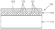
도 1을 참조하면, 본 발명의 일 실시예에 따른 투명 도전체(100)는 기재층(110), 투명 도전층(120)을 포함할 수 있다.Referring to FIG. 1, a
기재층(110)은 투명 도전층(120)을 지지하고 투명 도전층(120)을 보호할 수 있다. 기재층(110)은 파장 550nm에서 광 투과율이 85% 내지 100%, 더 구체적으로 90% 내지 99%인 수지 필름을 포함할 수 있다. 상기 범위에서, 투명 도전체의 광학 특성이 개선될 수 있다. 구체적으로, 수지는 폴리카보네이트, 시클릭올레핀폴리머, 폴리에틸렌테레프탈레이트, 폴리에틸렌나프탈레이트 등을 포함하는 폴리에스테르, 폴리올레핀, 폴리술폰, 폴리이미드, 실리콘(silicone), 폴리스티렌, 폴리아크릴, 폴리비닐클로라이드 수지 중 하나 이상을 포함할 수 있지만, 이에 제한되지 않는다. 기재층(110)은 두께가 10㎛ 내지 200㎛, 구체적으로 30㎛ 내지 150㎛, 더 구체적으로 30㎛ 내지 100㎛가 될 수 있다. 상기 범위에서, 기재층은 투명 도전체에 사용될 수 있다. 도 1은 기재층(110)이 단일층으로 되어 있으나 기재층은 다중층이 될 수도 있고, 도 1에서 도시되지 않았지만 기재층(110) 상에는 기능층이 형성될 수도 있다. 기능층은 하드 코팅, 부식 방지, 반사 방지, 부착력 증진, 올리고머 용출 방지 기능 등을 제공하는 것으로, 기재층과 독립적으로 별개의 층으로 형성되거나 또는 기재층의 일면이 기능층이 되도록 형성될 수도 있다.The
투명 도전층(120)은 기재층(110) 상에 형성되며, 투명 도전체(100)에 도전성과 유연성을 제공할 수 있다. 투명 도전층(120)은 기재층(110)에 직접적으로 형성될 수 있다.The transparent
투명 도전층(120)은 제1나노와이어 군(121), 제2나노와이어 군(122) 및 매트릭스(123)를 포함하고, 제1나노와이어 군(121)은 제2나노와이어 군(122)의 나노와이어 대비 길이가 작고, 제1나노와이어 군(121)과 제2나노와이어 군(122)의 나노와이어의 평균 길이의 비는 1:2 내지 1:4가 될 수 있다. 본 실시예의 투명 도전체(100)는 투명 도전층(120)에 서로 길이가 상이한 2종의 나노와이어를 포함함으로써 채널 저항 편차값이 낮아 채널 저항 균일도가 높고, 채널 형성 수율이 우수하며, 헤이즈가 낮아 광학 특성이 우수하고 면 저항이 낮을 수 있다. 구체적으로, 투명 도전체(100)는 채널 저항 편차값이 100% 이하, 구체적으로 30% 내지 90%, 파장 550nm에서 헤이즈가 1.0% 이하, 구체적으로 0.01% 내지 1.0%가 될 수 있다. 상기 범위에서, 투명 도전체를 패턴화하여 디스플레이 장치에 사용시 채널의 각도별로 채널 저항의 편차가 줄어들어 장치 구동에 더 유리할 수 있고, 광학디스플레이 장치에 사용하기에 더 용이할 수 있다.The transparent
제1나노와이어 군(121)은 투명 도전층(120)에 포함되며, 후술할 제2 나노와이어 군(122) 대비 길이가 작아 투명 도전층(120) 형성시 제2 나노와이어 군(122)이 한쪽 방향으로만 배향되는 것을 억제함으로써 투명 도전체(100)의 채널 저항 편차 값을 낮출 수 있다. 도 1은 제1나노와이어 군(121)이 투명 도전층(120)에 완전히 함침되는 경우를 예시하나 이에 제한되는 것은 아니며, 제1나노와이어 군(121)은 투명 도전층(120)의 외부에 일부 노출될 수도 있다. 도 1과 같이 제1나노와이어 군(121)이 투명 도전층(120)에 완전히 함침되는 경우 나노와이어의 산화가 감소할 수 있어 투명 도전체(100)의 면저항을 더 낮출 수 있다.The
제1나노와이어 군(121)은 길이가 1㎛ 이상 20㎛ 미만인 금속 나노와이어를 적어도 하나 이상 함유할 수 있다. 상기 범위에서, 투명 도전체의 채널 저항 편차 값을 낮추고 헤이즈와 면저항을 낮출 수 있다. 제1나노와이어 군(121)의 나노와이어의 평균 길이는 5㎛ 내지 18㎛, 구체적으로 5㎛ 내지 15㎛가 될 수 있다. 제1나노와이어 군(121)은 제1나노와이어 군(121)과 제2나노와이어 군(122) 전체 중 50중량% 미만, 구체적으로 10중량% 내지 30중량%로 포함될 수 있다. 상기 평균 길이 및 함량 범위에서, 투명 도전체의 채널 저항 편차값을 낮추고 헤이즈를 낮추어 광 특성을 좋게 할 수 있다. 금속 나노와이어는 종횡비가 10 내지 5000, 구체적으로 500 내지 1000, 더 구체적으로 500 내지 700이 될 수 있다. 금속 나노와이어는 단면의 직경이 0nm 초과 100nm 이하, 구체적으로 10nm 내지 100nm, 더 구체적으로 10nm 내지 30nm가 될 수 있다. 상기 종횡비 및 직경 범위에서, 높은 종횡비를 가져 투명 도전체의 전도성을 높이고 면 저항을 낮출 수 있다. 금속 나노와이어는 은, 구리, 알루미늄, 니켈, 금 중 하나 이상을 포함하는 금속으로 형성될 수 있고, 구체적으로 은 나노와이어를 포함할 수 있다.The first group of
제2나노와이어 군(122)은 투명 도전층(120)에 포함되며, 도전성 네트워크를 형성하여 투명 도전체(120)에 도전성을 제공하고, 면저항을 낮출 수 있다. 도 1은 제2나노와이어 군(122)이 투명 도전층(120)에 완전히 함침되는 경우를 예시하나 이에 제한되는 것은 아니며, 투명 도전층(120) 외부에 일부 노출될 수도 있다. 도 1과 같이 제2나노와이어 군(122)이 투명 도전층(120)에 완전히 함침되는 경우 나노와이어의 산화가 방지되어 막아 면저항을 더 낮출 수 있다.The second group of
제2나노와이어 군(122)은 길이가 20㎛ 이상 40㎛ 이하인 적어도 하나 이상의 금속 나노와이어를 함유할 수 있다. 상기 범위에서, 투명 도전체의 채널 저항 편차 값을 낮추고 헤이즈와 면저항을 낮출 수 있다. 제2나노와이어 군(122)의 나노와이어의 평균 길이는 20㎛ 내지 35㎛가 될 수 있다. 제2나노와이어 군(122)은 제1나노와이어 군(121)과 제2나노와이어 군(122) 중 50중량% 이상, 구체적으로 70중량% 내지 90중량%로 포함될 수 있다. 상기 평균 길이 및 함량 범위에서, 투명 도전체의 면저항을 낮추고 도전성을 좋게 할 수 있다. 제2나노와이어 군(122) 중 금속 나노와이어는 상술한 제1나노와이어 군(121)의 금속 나노와이어 대비 동일 또는 이종의 종횡비, 단면 직경, 금속 재료로 형성될 수 있다.The second group of
제1나노와이어 군(121)과 제2나노와이어 군(122) 전체는 투명 도전층(120) 중 40중량% 내지 80중량%, 구체적으로 50중량% 내지 70중량%로 포함될 수 있다. 상기 범위에서, 투명 도전체의 도전성을 높여 줄 수 있다.The entire
매트릭스(123)는 기재층(110) 상에 형성되어, 기재층(110)과 투명 도전층(120)의 결합을 강하게 하고, 제1나노와이어 군(121)과 제2나노와이어 군(122)을 함침시켜 금속 나노와이어의 산화를 방지하여 투명 도전체(100)의 면저항 상승을 막고, 투명 도전체(100)의 광학 특성, 내화학성, 내용매성, 내구성(신뢰성), 에칭성 등을 높일 수 있다.The
매트릭스(123)는 5관능 이상의 (메트)아크릴계 화합물, 2관능 또는3관능의 (메트)아크릴계 화합물, 및 개시제를 포함하는 매트릭스용 조성물로 형성될 수 있다.The
5관능 이상의 (메트)아크릴계 화합물은 5관능 내지 10관능 구체적으로 5관능 내지 6관능으로, (메트)아크릴계 모노머, (메트)아크릴계 올리고머 중 하나 이상을 포함할 수 있다. 5관능 이상의 (메트)아크릴계 모노머는 C3 내지 C20의 다가 알코올의 5관능 이상의 (메트)아크릴계 모노머를 함유하고, 디펜타에리트리톨펜타(메트)아크릴레이트, 디펜타에리트리톨헥사(메트)아크릴레이트, 카프로락톤 변성 디펜타에리트리톨펜타(메트)아크릴레이트, 카프로락톤 변성 디펜타에리트리톨헥사(메트)아크릴레이트 중 하나 이상을 포함할 수 있다. 5관능 이상의 (메트)아크릴계 올리고머는 5관능 이상의, 우레탄 (메트)아크릴레이트 올리고머, 폴리에스테르 (메트)아크릴레이트 올리고머, 에폭시 (메트)아크릴레이트 올리고머, 실리콘 함유 (메트)아크릴레이트 올리고머 중 하나 이상을 포함할 수 있다.The (meth) acrylic compound having five or more functional groups may include at least one of a (meth) acrylic monomer and a (meth) acrylic oligomer in a pentafunctionality to a tenth functionality, specifically a pentafunctionality or a hexafunctionality. The (meth) acrylate monomer having five or more functional groups is preferably a monomer containing at least a (meth) acrylic monomer having five or more functionalities of a polyhydric alcohol of C3 to C20 and having at least one of dipentaerythritol penta (meth) acrylate, dipentaerythritol hexa (meth) Caprolactone-modified dipentaerythritol penta (meth) acrylate, and caprolactone-modified dipentaerythritol hexa (meth) acrylate. The (meth) acrylic oligomer having five or more functional groups may be at least one of a urethane (meth) acrylate oligomer, a polyester (meth) acrylate oligomer, an epoxy (meth) acrylate oligomer, and a silicon containing (meth) acrylate oligomer .
2관능 또는 3관능 (메트)아크릴계 화합물은 비-우레탄계 2관능 또는 3관능 (메트)아크릴계 화합물로서, 비-개질된 C2 내지 C20의 다가알코올의 (메트)아크릴계 모노머, 알콕시기(예:C1 내지 C5의 알콕시기)로 개질된 C2 내지 C20의 다가알코올의 (메트)아크릴계 모노머 중 하나 이상을 포함할 수 있다. 비-개질된 C2 내지 C20의 다가알코올의 (메트)아크릴계 모노머는 트리메틸올프로판트리(메트)아크릴레이트, 글리세롤트리(메트)아크릴레이트, 펜타에리트리톨트리(메트)아크릴레이트, 디펜타에리트리톨트리(메트)아크릴레이트, 폴리에틸렌글리콜디(메트)아크릴레이트, 폴리프로필렌글리콜디(메트)아크릴레이트 중 하나 이상을 포함할 수 있다. 알콕시기로 개질된C2 내지 C20의 다가알코올의 (메트)아크릴계 모노머는 에톡시화된 트리메틸올프로판트리(메트)아크릴레이트, 프로폭시화된 글리세릴트리(메트)아크릴레이트 중 하나 이상을 포함할 수 있다. 5관능 이상의 (메트)아크릴계 화합물은 고형분 기준 매트릭스용 조성물 중 5중량% 내지 40중량%, 구체적으로 5중량% 내지 30중량%, 2관능 또는 3관능의 (메트)아크릴계 화합물은 고형분 기준 매트릭스용 조성물 중 25중량% 내지 85중량%, 구체적으로 25중량% 내지 60중량%로 포함될 수 있다. 상기 범위에서, 투명 도전체의 광 투과도와 신뢰성이 높을 수 있다. 본 명세서에서 "고형분"은 매트릭스용 조성물 중 용매를 제외한 나머지 전체를 의미한다.The bifunctional or trifunctional (meth) acrylic compound is a non-urethane-based bifunctional or trifunctional (meth) acrylic compound. The (meth) acrylic monomer may be a (meth) acrylic monomer or an alkoxy group of a non-modified C2 to C20 polyhydric alcohol (Meth) acrylic monomer of a C 2 to C 20 polyhydric alcohol modified with an alkyl (meth) acrylate or methacrylate (meth) acrylate. The (meth) acrylic monomers of the non-modified C2 to C20 polyhydric alcohols include trimethylol propane tri (meth) acrylate, glycerol tri (meth) acrylate, pentaerythritol tri (meth) acrylate, dipentaerythritol tri (Meth) acrylate, polyethylene glycol di (meth) acrylate, and polypropylene glycol di (meth) acrylate. The (meth) acrylic monomer of the C2 to C20 polyhydric alcohol modified with an alkoxy group may include one or more of ethoxylated trimethylol propane tri (meth) acrylate, propoxylated glyceryl tri (meth) acrylate . The (meth) acrylic compound having 5 or more functional groups is contained in an amount of 5 to 40% by weight, specifically 5 to 30% by weight, based on the weight of the solid matrix composition, and the bifunctional or trifunctional (meth) 25% by weight to 85% by weight, specifically 25% by weight to 60% by weight. Within the above range, the transparency of the transparent conductor can be high and reliability. As used herein, "solids" means the entirety of the composition for a matrix except for the solvent.
개시제는 광중합 개시제로서, 흡수 파장이 150nm 내지 500nm인 것이 될 수 있고, 알파-히드록시 케톤계 또는 알파-아미노 케톤계 중 하나 이상, 예를 들면 1-히드록시시클로헥실페닐케톤 또는 이를 포함하는 혼합물이 될 수 있다. 개시제는 고형분 기준 매트릭스용 조성물 중 1중량% 내지 15중량%, 구체적으로 1중량% 내지 11중량%로 포함될 수 있다. 상기 범위에서, 매트릭스용 조성물의 고형분이 완전히 경화될 수 있고, 잔량의 개시제가 남아서 투명 도전층의 광 특성이 떨어지는 것을 방지할 수 있다.The initiator may be a photopolymerization initiator having an absorption wavelength of 150 nm to 500 nm, and may be one or more of an alpha-hydroxy ketone type or alpha-amino ketone type, for example, 1-hydroxycyclohexyl phenyl ketone or a mixture . The initiator may be included in the composition for solid matrix-based matrices in an amount of 1 wt% to 15 wt%, specifically 1 wt% to 11 wt%. Within the above range, the solid content of the matrix composition can be completely cured, and the remaining amount of the initiator remains, thereby preventing the optical characteristics of the transparent conductive layer from deteriorating.
매트릭스용 조성물은 부착 증진제, 산화방지제, 무기 중공 입자 중 하나 이상을 더 포함할 수 있다.The composition for a matrix may further include at least one of an adhesion promoter, an antioxidant, and an inorganic hollow particle.
부착 증진제는 금속 나노와이어의 기재층에 대한 부착성을 증진시키고, 투명 도전체의 신뢰성을 높일 수 있다. 부착 증진제는 실란커플링제, 1관능의 (메트)아크릴계 모노머, 2관능의 (메트)아크릴계 모노머 중 하나 이상을 포함할 수 있다. 이들은 단독 또는 2종 이상 혼합하여 포함될 수 있다. 실란커플링제는 통상의 알려진 실란커플링제로, 3-글리시드옥시프로필트리메톡시실란 등의 에폭시기를 갖는 실란커플링제; 비닐트리메톡시실란 등의 중합성 불포화기 함유 실란커플링제; 3-아미노프로필트리메톡시실란, 3-아미노프로필트리에톡시실란 등의 아미노기 함유 실란커플링제; 및 3-클로로프로필트리메톡시실란 중 하나 이상을 사용할 수 있다. 1관능 또는 2관능의 (메트)아크릴계 모노머는 C3 내지 C20의 다가알코올의, 1관능 또는 2관능의 (메트)아크릴계 모노머로서, 이소보르닐(메트)아크릴레이트, 사이클로펜틸(메트)아크릴레이트, 사이클로헥실(메트)아크릴레이트, 트리메틸올프로판디(메트)아크릴레이트, 에틸렌글리콜디(메트)아크릴레이트, 네오펜틸글리콜디(메트)아크릴레이트, 헥산디올디(메트)아크릴레이트, 사이클로데칸디메탄올디(메트)아크릴레이트 중 하나 이상을 포함할 수 있다. 부착증진제는 고형분 기준 매트릭스용 조성물 중 1중량% 내지 20중량%, 구체적으로 5중량% 내지 15중량%로 포함될 수 있다. 상기 범위에서, 투명 도전체의 신뢰성과 도전성을 좋게 하고, 투명 도전층의 부착성을 좋게 할 수 있다.The adhesion promoter improves the adhesion of the metal nanowire to the base layer and can improve the reliability of the transparent conductor. The adhesion promoter may include at least one of a silane coupling agent, a monofunctional (meth) acrylic monomer, and a bifunctional (meth) acrylic monomer. These may be included singly or in combination of two or more. The silane coupling agent is a commonly known silane coupling agent, and includes silane coupling agents having an epoxy group such as 3-glycidoxypropyltrimethoxysilane; A silane coupling agent containing a polymerizable unsaturated group such as vinyltrimethoxysilane; Amino group-containing silane coupling agents such as 3-aminopropyltrimethoxysilane and 3-aminopropyltriethoxysilane; And 3-chloropropyltrimethoxysilane can be used. The monofunctional or bifunctional (meth) acrylic monomer is a monofunctional or bifunctional (meth) acrylic monomer of C3 to C20 polyalcohol, such as isobornyl (meth) acrylate, cyclopentyl (meth) (Meth) acrylate, cyclohexyl (meth) acrylate, trimethylolpropane di (meth) acrylate, ethylene glycol di (meth) acrylate, neopentyl glycol di Di (meth) acrylate, and the like. The adhesion promoting agent may be included in the composition for solid matrix-based matrices in an amount of 1 wt% to 20 wt%, specifically 5 wt% to 15 wt%. Within the above range, the reliability and conductivity of the transparent conductor can be improved, and the adhesion of the transparent conductive layer can be improved.
산화방지제는 금속 나노와이어의 네트워크의 산화를 방지할 수 있다. 산화방지제는 트리아졸계, 트리아진계, 포스파이트계 등의 인계, HALS(Hinder amine light stabilizer)계, 페놀계, 금속 아세틸아세토네이트계 산화방지제 중 하나 이상을 포함할 수 있다. 이들은 단독 또는 2종 이상 혼합하여 포함될 수 있다. 구체적으로, 인계 산화방지제는 트리스(2,4-디-터트-부틸페닐)포스파이트, 페놀계 산화방지제는 펜타에리트리톨테트라키스(3-(3,5-디-터트-부틸-4-히드록시페닐)프로피오네이트)가 될 수 있다. HALS계 산화방지제는 비스(2,2,6,6-테트라메틸-4-피페리딜)세바케이트, 비스(2,2,6,6-테트라메틸-4-피페리디닐)세바케이트, 비스(2,2,6,6-테트라메틸-5-피페리디닐)세바케이트, 4-히드록시-2,2,6,6-테트라메틸-1-피페리딘-에탄올을 갖는 디메틸숙시네이트 공중합체, 2,4-비스[N-부틸-N-(1-시클로헥실옥시-2,2,6,6-테트라메틸피페리딘-4-일)아미노]-6-(2-히드록시에틸아민)-1,3,5-트리아진 등을 포함할 수 있지만, 이에 제한되지 않는다. 금속 아세틸아세토네이트계 산화방지제는 트리스(아세틸아세토네이토)철(III), 트리스(아세틸아세토네이토)크롬(III) 등을 포함할 수 있지만, 이에 제한되지 않는다. 산화방지제는 고형분 기준 매트릭스용 조성물 중 0.01중량% 내지 10중량%, 구체적으로 0.5중량% 내지 7중량%로 포함될 수 있다. 상기 범위에서, 금속 나노와이어의 산화를 방지하고, 패터닝된 투명 도전체의 패턴 균일도가 높고 미세 패턴의 구현에 유리할 수 있다.Antioxidants can prevent oxidation of the network of metal nanowires. The antioxidant may include one or more of triazole-based, triazine-based, phosphite-based phosphorus, Hindered amine light stabilizer (HALS) based, phenol based, and metal acetylacetonate based antioxidant. These may be included singly or in combination of two or more. Specifically, the phosphorus antioxidant is tris (2,4-di-tert-butylphenyl) phosphite and the phenol antioxidant is pentaerythritol tetrakis (3- (3,5- Roxy phenyl) propionate). The antioxidant for HALS is bis (2,2,6,6-tetramethyl-4-piperidyl) sebacate, bis (2,2,6,6-tetramethyl-4- piperidinyl) sebacate, bis (2,2,6,6-tetramethyl-5-piperidinyl) sebacate, dimethyl succinate having 4-hydroxy-2,2,6,6-tetramethyl-1-piperidin- N-butyl-N- (1-cyclohexyloxy-2,2,6,6-tetramethylpiperidin-4-yl) amino] -6- Ethylamine) -1,3,5-triazine, and the like. The metal acetylacetonate antioxidant may include, but is not limited to, tris (acetylacetonato) iron (III), tris (acetylacetonato) chromium (III), and the like. The antioxidant may be contained in the composition for solid matrix-based matrices in an amount of 0.01 wt% to 10 wt%, specifically 0.5 wt% to 7 wt%. In this range, oxidation of the metal nanowires is prevented, pattern uniformity of the patterned transparent conductor is high, and it is advantageous for realizing a fine pattern.
무기 중공 입자는 굴절률이 1.4 이하, 구체적으로 1.33 내지 1.38이 될 수 있다. 무기 중공 입자의 평균입경(D50)은 30nm 내지 100nm, 구체적으로 40nm 내지 70nm일 수 있다. 상기 범위에서 매트릭스에 포함될 수 있으며, 투명 도전층으로 적용하기에 유리할 수 있다. 무기 중공 입자는 실리카, 멀라이트(mullite), 알루미나, 실리콘 카바이드(SiC), MgO-Al2O3-SiO2, Al2O3-SiO2, MgO-Al2O3-SiO2-LiO2, 또는 이들의 혼합물을 포함할 수 있고, 이들은 표면 처리된 것일 수도 있다. 무기 중공 입자는 입자 자체로 포함될 수도 있으나, 무기 중공 입자 함유 용액으로 포함되어도 무방하다. 무기 중공 입자는 매트릭스용 조성물 중 고형분에 대하여 10중량% 내지 50중량%, 15중량% 내지 50중량%로 포함될 수 있다. 상기 범위에서, 투명 도전체의 투과 b*값을 낮추고 투과도를 높일 수 있다.The inorganic hollow particles may have a refractive index of 1.4 or less, specifically 1.33 to 1.38. The average particle size (D50) of the inorganic hollow particles may be 30 nm to 100 nm, specifically 40 nm to 70 nm. May be included in the matrix within the above range, and may be advantageously applied as a transparent conductive layer. The inorganic hollow particles may be selected from the group consisting of silica, mullite, alumina, silicon carbide (SiC), MgO-Al 2 O 3 -SiO 2 , Al 2 O 3 -SiO 2 , MgO-Al 2 O 3 -SiO 2 -LiO 2 , Or a mixture thereof, and they may be surface-treated. The inorganic hollow particles may be contained in the particles themselves, but may be contained in the solution containing the inorganic hollow particles. The inorganic hollow particles may be present in the matrix composition in an amount of from 10% 50% by weight, and 15% by weight to 50% by weight. In the above range, the transmission b * value of the transparent conductor can be lowered and the transmittance can be increased.
매트릭스용 조성물은 용매를 더 포함할 수 있다. 용매는 메틸이소부틸케톤 등의 케톤계 용매, 이소프로필알코올, 에탄올 등의 알코올계 용매 중 하나 이상을 포함할 수 있다. 매트릭스용 조성물은 첨가제를 더 포함할 수 있다. 첨가제는 대전방지제, 자외선 흡수제, 점도 조절제, 열 안정제, 분산제, 증점제 등을 포함할 수 있다.The composition for a matrix may further comprise a solvent. The solvent may include at least one of ketone solvents such as methyl isobutyl ketone, and alcohol solvents such as isopropyl alcohol and ethanol. The composition for a matrix may further comprise an additive. The additives may include antistatic agents, ultraviolet absorbers, viscosity modifiers, heat stabilizers, dispersants, thickeners, and the like.
매트릭스용 조성물은 25℃에서 점도가 0.1cP 내지 20cP가 될 수 있다. 상기 범위에서, 매트릭스용 조성물의 코팅성을 좋게 하고, 균일하게 박막으로 코팅되도록 하여 투명 도전층이 균일한 물리, 화학적 특성을 내도록 할 수 있다.The composition for a matrix may have a viscosity of 0.1 cP to 20 cP at 25 캜. Within the above range, the coating property of the matrix composition is improved and uniformly coated with a thin film, so that the transparent conductive layer can have uniform physical and chemical properties.
투명 도전층(120)은 두께가 10nm 내지 1㎛, 구체적으로 10nm 내지 200nm가 될 수 있다. 상기 범위에서, 광학 디스플레이 장치에 사용될 수 있다.The transparent
투명 도전체(100)는 가시광선 영역 예를 들면 파장 400nm 내지 700nm에서 투명성을 가질 수 있다. 구체적으로, 투명 도전체(100)는 전광선 투과율이 90% 이상, 구체적으로 90% 내지 99%일 수 있다. 상기 범위에서, 투명성이 좋아 투명 도전체로 사용될 수 있다. 투명 도전체(100)는 4-프로브(probe) 또는 비접촉식 면 저항 측정기로 측정된 면 저항이 100Ω/□ 이하, 구체적으로 30Ω/□ 내지 100Ω/□, 더 구체적으로 30Ω/□ 내지 55Ω/□일 수 있다. 상기 범위에서, 면 저항이 낮아 터치패널용 전극 필름으로 사용할 수 있고, 대면적 터치 패널에 적용될 수 있다. 투명 도전체(100)의 두께는 10㎛ 내지 250㎛, 구체적으로 50㎛ 내지 200㎛일 수 있다. 상기 범위에서, 터치패널용 필름을 포함하는 투명 전극 필름으로 사용할 수 있고, 플렉서블 터치 패널용 투명 전극필름으로 사용될 수 있다. 투명 도전체(100)는 필름 형태로서, 에칭 등에 의해 패터닝되어, 터치 패널, E-paper, 또는 태양 전지의 투명 전극 필름으로 사용될 수 있다.The
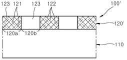
이하, 본 발명의 다른 실시예에 따른 투명 도전체를 도 2를 참고하여 설명한다. 도 2는 본 발명의 다른 실시예에 따른 투명 도전체의 단면도이다.Hereinafter, a transparent conductor according to another embodiment of the present invention will be described with reference to FIG. 2 is a cross-sectional view of a transparent conductor according to another embodiment of the present invention.
도 2를 참고하면, 본 실시예의 투명 도전체(100')는 투명 도전층(120')이 투명 도전성층(120a)과, 매트릭스(123)만 포함하는 투명 비도전성층(120b)으로 패턴화된 점을 제외하고는 본 발명의 일 실시예의 투명 도전체(100)와 실질적으로 동일하다. 투명 도전층(120')은 본 발명의 일 실시예에 따른 투명 도전층(120)을 통상의 방법으로 패턴화하여 형성될 수 있다. 구체적으로, 패턴화는 투명 도전층(120) 상에 포토레지스트층을 형성하고, 패턴이 형성된 마스크를 포토레지스트층 상에 놓고, UV 노광하고, 현상하고, 베이킹하고, 에칭하는 것을 포함할 수 있다.2, the transparent conductor 100 'of the present embodiment is formed by patterning a transparent conductive layer 120' into a transparent
이하, 도 3을 참고하여 본 발명의 일 실시예에 따른 광학표시장치를 설명한다. 도 3은 본 발명의 일 실시예에 따른 광학표시장치의 단면도이다.Hereinafter, an optical display device according to an embodiment of the present invention will be described with reference to FIG. 3 is a cross-sectional view of an optical display device according to an embodiment of the present invention.
도 3을 참고하면, 본 발명의 일 실시예에 따른 광학표시장치(200)는 디스플레이부(210), 편광판(220), 투명 전극체(230), 윈도우 필름(240), 점착층(250)을 포함하고, 투명 전극체(230)는 본 발명의 실시예들에 따른 투명 도전체로 형성될 수 있다. 도 3은 디스플레이부(210), 편광판(220), 투명 전극체(230), 윈도우 필름(240)의 순서로 적층된 구조를 도시한 것이나, 디스플레이부(210), 투명 전극체(230), 편광판(220), 윈도우 필름(240)의 순서로 적층된 구조도 가능할 수 있다.3, an
디스플레이부(210)는 광학표시장치(200)를 구동시키기 위한 것으로, 기판 및 기판 상에 형성된 OLED, LED 또는 LCD 소자를 포함하는 광학 소자를 포함할 수 있다. 일 구체예에서, 디스플레이부(210)는 하부기판, 박막 트랜지스터, 유기발광다이오드, 평탄화층, 보호막, 절연막을 포함할 수 있다. 다른 구체예에서, 디스플레이부(210)는 상부기판, 하부기판, 상부 기판과 하부 기판 사이에 위치된 액정층, 및 상부기판, 하부기판 중 하나 이상에 형성된 칼라필터를 포함할 수 있다. 도 3은 디스플레이부(210)와 투명 전극체(230)가 별개의 독립적으로 적층된 구조를 나타낸 것이나, 디스플레이부 내부에 투명 전극체(230)가 형성될 수도 있다.The
편광판(220)은 디스플레이부(210) 상에 형성되어, 내광의 편광을 구현하거나 또는 외광의 반사를 방지하여 디스플레이를 구현하거나 디스플레이의 명암비를 좋게 할 수 있다. 편광판(220)은 편광자 단독이 될 수 있다. 또는, 편광판(220)은 편광자 및 편광자의 일면 또는 양면에 형성된 보호필름을 포함할 수 있다. 도 3에서 도시되지 않았지만, 디스플레이부(210)의 하부에도 편광판이 더 형성되어, 디스플레이의 명암비를 더 좋게 할 수 있다. 이때, 편광판은 점착층에 의해 디스플레이부(210)에 형성될 수 있다.The
투명 전극체(230)는 편광판(220) 상에 형성되어, 접촉 등에 의해 투명 전극체(230)가 터치될 때 발생되는 커패시턴스의 변화를 감지하여 전기적 신호를 발생시킬 수 있다. 투명 전극체(230)는 기재층(110), 기재층(110)의 일면에 형성된 제1전극(231)과 제2전극(232), 기재층(110)의 다른 일면에 형성된 제3전극(233)과 제4전극(234)을 포함할 수 있다. 도 3은 제3전극(233)과 제4전극(234)/기재층(110)/제1전극(231)과 제2전극(232)의 순서로 적층된 구조를 나타낸 것이나, 기재층(110)/제3전극(233)과 제4전극(234)/기재층(110)/ 제1전극(231)과 제2전극(232)의 순서로 적층될 수도 있다.The
윈도우 필름(240)은 광학표시장치(200)의 최 외곽에 형성되어 광학표시장치(200)를 보호할 수 있다. 윈도우 필름(240)은 유리 기판, 또는 유연성이 있는 플라스틱 기판으로 형성될 수 있다.The
점착층(250)은 디스플레이부(210)와 편광판(220) 사이, 편광판(220)과 투명 전극체(230) 사이, 투명 전극체(230)와 윈도우 필름(240) 사이에 형성되어, 디스플레이부(210), 편광판(220), 투명 전극체(230), 윈도우 필름(240) 간의 결합을 강하게 할 수 있다. 점착층(250)은 통상의 광학적으로 투명한 점착제로 형성될 수 있다. The
이하, 도 4를 참고하여, 본 발명의 다른 실시예에 따른 광학표시장치를 설명한다. 도 4는 본 발명의 다른 실시예에 따른 광학표시장치의 단면도이다.Hereinafter, an optical display device according to another embodiment of the present invention will be described with reference to FIG. 4 is a cross-sectional view of an optical display device according to another embodiment of the present invention.
도 4를 참고하면, 본 발명의 다른 실시예에 따른 광학표시장치(300)는 투명 전극체(230')가 기재층(110), 기재층(110)의 일면에 형성된 제3전극(233)과 제4전극(234)을 포함하고, 윈도우 필름(240')에 제1전극(231)과 제2전극(232)이 더 형성된 것을 제외하고는 본 발명의 일 실시예에 따른 광학표시장치(200)와 실질적으로 동일하다.4, an
이하, 본 발명의 일 실시예에 따른 투명 도전체의 제조 방법을 설명한다.Hereinafter, a method of manufacturing a transparent conductor according to an embodiment of the present invention will be described.
본 발명의 일 실시예에 따른 투명 도전체의 제조 방법은 금속 나노와이어 분산액을 기재층 상에 코팅하여 금속 나노와이어 분산액 층을 형성하고, 상기 금속 나노와이어 분산액 층 상에 매트릭스용 조성물을 코팅하고, 상기 금속 나노와이어 분산액 층과 매트릭스용 조성물을 경화시키는 단계를 포함할 수 있다.A method of manufacturing a transparent conductor according to an exemplary embodiment of the present invention includes coating a metal nanowire dispersion on a base layer to form a metal nanowire dispersion layer, coating the matrix composition on the metal nanowire dispersion layer, And curing the metal nanowire dispersion layer and the composition for a matrix.
금속 나노와이어 분산액은 제1나노와이어 군 분산액과 제2나노와이어 군 분산액을 혼합하여 제조될 수 있다. 제2나노와이어 군 분산액은 상업적으로 시판되는 Cambrios사의 제품(예:ClearOhm Ink)을 사용할 수 있지만, 이에 제한되지 않는다. 제1나노와이어 군 분산액은 상업적으로 구입할 수도 있고 또는 제2나노와이어 군 분산액을 프로브 소니케이터로 처리하여 나노와이어를 절단함으로써 제조될 수 있다. 이때, 제1나노와이어 군 분산액과 제2나노와이어 군 분산액 중 나노와이어의 평균 길이의 비가 1:2 내지 1:4가 되도록 프로브 소니케이터 처리 시간 및/또는 파워를 조절할 수 있다. 제1나노와이어 군 분산액과 제2나노와이어 군 분산액의 총합 100중량부 중, 제1나노와이어 군 분산액은 50중량부 미만 구체적으로 10중량부 내지 30중량부, 제2나노와이어 군 분산액은 50중량부 이상 구체적으로 70중량부 내지 90중량부로 포함될 수 있다.The metal nanowire dispersion can be prepared by mixing the dispersion of the first nanowire group and the dispersion of the second nanowire group. The second nanowire group dispersion can be, but is not limited to, commercially available products from Cambrios (e.g. ClearOhm Ink). The first nanowire group dispersion may be commercially available or may be prepared by treating the second nanowire group dispersion with a probe sonicator to cut the nanowires. At this time, the probe sonicator processing time and / or power can be adjusted so that the ratio of the average length of the nanowires in the dispersion of the first nanowire group dispersion and the dispersion of the second nanowire group is 1: 2 to 1: 4. The first nanowire group dispersion is less than 50 parts by weight, specifically 10 parts by weight to 30 parts by weight, and the second nanowire group dispersion is 50 parts by weight, the total amount of the first nanowire group dispersion and the second nanowire group dispersion is 100 parts by weight Or more and specifically 70 parts by weight to 90 parts by weight.
금속 나노와이어 분산액은 용매를 더 포함하여 금속 나노와이어의 코팅성을 더 높일 수 있다. 용매는 물, 알코올 등의 유기 용매 등을 포함할 수 있지만, 이에 제한되지 않는다. 금속 나노와이어 분산액은 바인더, 개시제, 첨가제 등을 더 포함할 수도 있다. 첨가제는 분산제, 증점제 등이 될 수 있다. 바인더는 (메트)아크릴레이트계 단관능 모노머, (메트)아크릴레이트계 다관능 모노머 중 하나 이상을 포함할 수 있다. 분산제는 금속 나노와이어, 바인더의 분산을 높일 수 있다. 증점제는 금속 나노와이어 분산액의 점도를 높일 수 있다. 바인더, 개시제, 및 첨가제 전체는 금속 나노와이어 분산액 중 고형분 기준으로 0.1중량% 내지 50중량%, 구체적으로 5중량% 내지 45중량%로 포함될 수 있다. 상기 범위에서, 투명 도전체의 광 특성 향상, 접촉 저항 증가 방지, 내구성 및 내 화학성이 개선될 수 있다.The metal nanowire dispersion may further include a solvent to further enhance the coating properties of the metal nanowire. The solvent may include, but is not limited to, water, an organic solvent such as alcohol, and the like. The metal nanowire dispersion may further contain a binder, an initiator, an additive, and the like. The additives may be dispersants, thickeners, and the like. The binder may include at least one of a (meth) acrylate-based monofunctional monomer and a (meth) acrylate-based polyfunctional monomer. The dispersing agent can increase the dispersion of the metal nanowires and the binder. Thickening agents can increase the viscosity of the metal nanowire dispersion. The binder, initiator, and additives may be included in the metal nanowire dispersion in an amount of 0.1 wt% to 50 wt%, specifically 5 wt% to 45 wt% based on solids. Within the above range, improvement of optical characteristics, prevention of increase in contact resistance, durability and chemical resistance of the transparent conductor can be improved.
매트릭스용 조성물은 5관능 이상의 (메트)아크릴계 화합물, 2관능 또는 3관능의 (메트)아크릴계 화합물 등을 혼합하여 제조될 수 있다. 부착증진제, 산화방지제, 무기 중공 입자 또는 무기 중공 입자 함유 용액, 첨가제, 용매 등이 매트릭스용 조성물에 더 포함될 수도 있다.The composition for a matrix may be prepared by mixing a (meth) acrylic compound having five or more functional groups, a bifunctional or trifunctional (meth) acrylic compound, and the like. An adhesion promoting agent, an antioxidant, a solution containing an inorganic hollow particle or an inorganic hollow particle, an additive, a solvent and the like may further be contained in the composition for a matrix.
그런 다음, 금속 나노와이어 분산액을 기재층 상에 코팅하여 금속 나노와이어 분산액 층을 형성하고, 상기 금속 나노와이어 분산액 층 상에 매트릭스용 조성물을 코팅하고, 금속 나노와이어 분산액 층과 매트릭스용 조성물을 경화시킴으로써 투명 도전층을 형성할 수 있다. 코팅은 바 코팅, 슬롯 다이 코팅, 그라비아 코팅, 롤-투-롤(roll-to-roll) 코팅으로 수행될 수 있지만, 이에 제한되지 않는다. 코팅 두께는 10nm 내지 1㎛, 구체적으로 20nm 내지 150nm, 더 구체적으로 50nm 내지 130 nm 또는 70nm 내지 120nm가 될 수 있다. 경화는 투명 도전층을 형성하고 투명 도전층의 강도를 높일 수 있다. 경화는 열 경화, 광 경화 중 하나 이상을 포함할 수 있다. 열 경화는 40℃ 내지 180℃, 1분 내지 48시간 동안 수행될 수 있다. 광경화는 UV 조사량 50mJ/cm2 내지 1,000mJ/cm2으로 수행될 수 있다. 투명 도전층용 도막을 경화시키기 전에 투명 도전층용 도막을 건조시켜, 경화 시간을 단축시킬 수 있다. 건조는 40℃ 내지 180℃, 1분 내지 48시간 동안 수행될 수 있다.The metal nanowire dispersion is then coated on the substrate layer to form a metal nanowire dispersion layer, the composition for the matrix is coated on the metal nanowire dispersion layer, and the metal nanowire dispersion layer and the matrix composition are cured A transparent conductive layer can be formed. The coating can be performed by, but not limited to, bar coating, slot die coating, gravure coating, and roll-to-roll coating. The coating thickness can be from 10 nm to 1 탆, specifically from 20 nm to 150 nm, more specifically from 50 nm to 130 nm or from 70 nm to 120 nm. The curing can form a transparent conductive layer and increase the strength of the transparent conductive layer. The curing may include one or more of thermosetting, photo-curing. The thermal curing may be carried out at 40 캜 to 180 캜 for 1 minute to 48 hours. Photocuring can be carried out with a UV dose of 50 mJ / cm 2 to 1,000 mJ / cm 2 . The coating film for a transparent conductive layer can be dried before curing the coating film for a transparent conductive layer to shorten the curing time. Drying may be carried out at 40 캜 to 180 캜 for 1 minute to 48 hours.
이하, 본 발명의 바람직한 실시예를 통해 본 발명의 구성 및 작용을 더욱 상세히 설명하기로 한다. 다만, 이는 본 발명의 바람직한 예시로 제시된 것이며 어떠한 의미로도 이에 의해 본 발명이 제한되는 것으로 해석될 수는 없다.Hereinafter, the configuration and operation of the present invention will be described in more detail with reference to preferred embodiments of the present invention. It is to be understood, however, that the same is by way of illustration and example only and is not to be construed in a limiting sense.
실시예Example 1 One
은 나노와이어의 길이가 20㎛ 내지 30㎛(은 나노와이어의 평균 길이:약 24㎛)인 다수의 은 나노와이어가 분산되어 있는 제2나노와이어 군 분산액(Clearohm ink, Cambrios사)을 준비하였다. 상기 제2나노와이어 군 분산액을 프로브 소니케이터에서 power 20%로 20초 동안 처리하여 제1나노와이어 군 분산액(은 나노와이어의 길이: 10㎛ 내지 15㎛, 은 나노와이어의 평균 길이:약 12㎛)을 제조하였다. 은 나노와이어의 평균 길이는 SEM으로 측정되었다.A second nanowire group dispersion (Clearohm ink, Cambrios) in which a plurality of silver nanowires having a length of nanowires of 20 mu m to 30 mu m (silver nanowire average length: about 24 mu m) was dispersed was prepared. The dispersion of the second nanowire group was treated with a power of 20% in a probe sonicator for 20 seconds to obtain a dispersion of the first nanowire group (length of the silver nanowire: 10 탆 to 15 탆, average length of the silver nanowire: about 12 Mu m). The average length of the silver nanowires was measured by SEM.
제1나노와이어 군 분산액 10중량부와 제2나노와이어 군 분산액 90중량부를 혼합하고, 용제 물을 소정량 첨가하여, 은 나노와이어 분산액(고형분 농도:0.9%)을 제조하였다.10 parts by weight of the dispersion of the first nanowire group and 90 parts by weight of the dispersion of the second nanowire group were mixed and a predetermined amount of solvent was added to prepare a silver nanowire dispersion (solid concentration: 0.9%).
디펜타에리트리톨헥사아크릴레이트(DPHA, Entis사) 12.7중량부, 폴리에틸렌글리콜디아크릴레이트(SR344, Sartomer사) 38.2중량부, 부착증진제로 3-아미노프로필트리에톡시실란(KBE-903, 신에츠사) 8.5중량부, 산화방지제로 페놀계 산화방지제 Irganox 1010, 인계 산화방지제 Irgafos 168(BASF사) 및 트리스(아세틸아세토네이트)철(III)(Sigma Aldrich사)의 혼합물 4.9중량부, 개시제로 Irgacure 184(CIBA사) 1.7중량부, 중공 실리카(A-2505(실리카 고형분10중량%를 포함하는 용액), Plenox) 34 중량부를 포함하는 고형분 100중량부의 혼합물 중 1.6중량부를 용매인 메틸이소부틸케톤 98.4중량부에 첨가하여 25℃에서 점도 0.56cP의 매트릭스용 조성물을 제조하였다.12.7 parts by weight of dipentaerythritol hexaacrylate (DPHA, Entis), 38.2 parts by weight of polyethylene glycol diacrylate (SR344, Sartomer), 3-aminopropyltriethoxysilane (KBE-903, , 4.9 parts by weight of a mixture of phenolic antioxidant Irganox 1010, phosphorus antioxidant Irgafos 168 (BASF) and tris (acetylacetonate) iron (III) (Sigma Aldrich) as antioxidants, Irgacure 184 , 1.6 parts by weight of a mixture of 100 parts by weight of a solid component containing 1.7 parts by weight of a binder resin (CIBA) and 34 parts by weight of hollow silica (A-2505 (solution containing 10% by weight of silica solid content), Plenox) was dissolved in 98.4 weight parts of methyl isobutyl ketone To prepare a composition for a matrix having a viscosity of 0.56 cP at 25 캜.
기재층(폴리카보네이트 필름, Teijin, 두께:50㎛)에, 제조한 은 나노와이어 분산액을 스핀 코터로 코팅하고, 140℃ 오븐에서 90초 건조시키고, 이어서 제조한 매트릭스용 조성물을 바 코터로 코팅한 후, 80℃ 오븐에서 90초, 120℃ 오븐에서 90초 건조 후, 200mJ/cm2으로 UV 경화시켜, 두께 90nm의 투명 도전층을 형성함으로써, 투명 도전체를 제조하였다.The prepared silver nanowire dispersion liquid was coated on a substrate layer (polycarbonate film, Teijin, thickness: 50 占 퐉) by a spin coater, dried in an oven at 140 占 폚 for 90 seconds, and then coated with a bar coater Thereafter, the substrate was dried in an oven at 80 ° C for 90 seconds, dried in an oven at 120 ° C for 90 seconds, and then UV-cured at 200 mJ / cm 2 to form a transparent conductive layer having a thickness of 90 nm.
실시예Example 2와 2 and 실시예Example 3, 3, 비교예Comparative Example 1 One
실시예 1에서, 하기 표 1의 중량부로 제조된 은 나노와이어 분산액을 사용한 것을 제외하고는 동일한 방법으로, 투명 도전체를 제조하였다.A transparent conductor was prepared in the same manner as in Example 1, except that the silver nanowire dispersion liquid prepared in the weight parts of the following Table 1 was used.
비교예Comparative Example 2 2
실시예 1에서, 제2나노와이어 군 분산액을 프로브 소니케이터에서 power 40%로 20초 동안 처리하여 제3나노와이어 군 분산액(은 나노와이어의 길이: 3㎛ 내지 8㎛, 은 나노와이어의 평균 길이: 약 5㎛)을 제조하였다. 실시예 1에서, 하기 표 1의 중량부로 제조된 은 나노와이어 분산액을 사용한 것을 제외하고는 동일한 방법으로, 투명 도전체를 제조하였다.In Example 1, the dispersion of the second nanowire group was treated in a probe sonicator at a power of 40% for 20 seconds to obtain a dispersion of the third nanowire group (silver nanowires having a length of 3 탆 to 8 탆, silver nanowires averaged Length: about 5 탆). A transparent conductor was prepared in the same manner as in Example 1, except that the silver nanowire dispersion liquid prepared in the weight parts of the following Table 1 was used.
비교예Comparative Example 3 3
실시예 1에서, 제2나노와이어 군 분산액을 프로브 소니케이터에서 power 10%로 20초 동안 처리하여 제4나노와이어 군 분산액(은 나노와이어의 길이: 15㎛ 내지 20㎛, 은 나노와이어의 평균 길이:약 18㎛)을 제조하였다.In Example 1, the dispersion of the second nanowire group was treated in a probe sonicator at a power of 10% for 20 seconds to obtain a dispersion of the fourth nanowire group (silver nanowires having a length of 15 mu m to 20 mu m, Length: about 18 mu m).
실시예 1에서, 하기 표 1의 중량부로 제조된 은 나노와이어 분산액을 사용한 것을 제외하고는 동일한 방법으로, 투명 도전체를 제조하였다.A transparent conductor was prepared in the same manner as in Example 1, except that the silver nanowire dispersion liquid prepared in the weight parts of the following Table 1 was used.
실시예와 비교예의 투명 도전체에 대해 하기 물성을 평가하고, 그 결과를 하기 표 1에 나타내었다.The following properties of the transparent conductor of the examples and comparative examples were evaluated, and the results are shown in Table 1 below.
(1)면저항: 투명 도전체에 대해 비접촉식 면저항 측정기(EC-80P, NAPSON)를 사용하여 면저항을 측정하였다. 면저항은 패터닝하지 않은 투명 도전층에 대해 측정하였다.(1) Surface resistance: The sheet resistance was measured using a non-contact type surface resistivity meter (EC-80P, NAPSON) for the transparent conductor. The sheet resistance was measured for a transparent conductive layer that was not patterned.
(2)헤이즈와 전광선 투과율: 투명 도전체에 대해 도전층을 광원으로 향하게 하고 파장 400nm 내지 700nm에서 헤이즈미터(NDH-2000, NIPPON DENSHOKU)를 사용하여 헤이즈와 전광선 투과율을 측정하였다.(2) Haze and total light transmittance: Haze and total light transmittance were measured using a haze meter (NDH-2000, NIPPON DENSHOKU) at a wavelength of 400 nm to 700 nm with the conductive layer directed toward the light source for the transparent conductor.
(3)채널 저항(Rx, Ry) 및 채널 저항 편차값: 투명 도전체에 포토레지스트 필름(동우화인켐, SS-03A9)을 스핀 코팅하고 120℃ 오븐에서 3분간 건조시키고, 패턴 마스크를 사용하여 200mJ/cm2로 자외선 노광한 후 트리메틸암모늄 하이드록사이드 5% 수용액에 넣고 10초 동안 현상하고, 120℃ 오븐에서 3분간 베이킹하고, 에칭액(Al etchant, Transene사 Aluminum etchant type A))에 침지하여 에칭하여 패턴화된 투명 도전체를 제조하였다. 은 나노와이어가 코팅된 방향을 x축, x축과 수직인 방향을 y축이라고 할 때, 패턴화된 투명 도전체의 은 나노와이어를 함유하는 부분 중 x축 방향과 y축 방향 각각으로 멀티미터(Sanwa社, CD800a)를 사용하여 저항 측정 길이 70mm로 채널 저항(선저항) Rx, Ry을 측정하고, 상기 식 1에 따라 계산하였다. (3) Channel resistance (R x , R y ) and channel resistance deviation value: A photoresist film (Dongwoo Fine-Chem, SS-03A9) was spin-coated on the transparent conductor and dried in an oven at 120 ° C for 3 minutes. after the ultraviolet light exposure at 200mJ / cm 2 using ammonium hydroxide developer for 5% aqueous solution into 10 seconds, and, and 3 minutes and baked at 120 ℃ oven, an etching solution (Al etchant, Transene Co. Aluminum etchant type a)) Followed by dipping and etching to prepare a patterned transparent conductor. And a direction perpendicular to the x-axis is a y-axis, a direction in which the nanowire is coated is defined as x-axis and a direction perpendicular to the x- (Line resistance) R x and R y were measured at a resistance measurement length of 70 mm by using a resistivity measuring device (Sanwa, CD800a) and calculated according to the above-mentioned formula 1.
(Ω/□)Sheet resistance
(Ω / □)
(%)Hayes
(%)
(%)Total light transmittance
(%)
(kΩ)R x
(kΩ)
(kΩ)R y
(kΩ)
(%)Channel resistance deviation value
(%)
1:2A: B
1: 2
1:2A: B
1: 2
1:2A: B
1: 2
1:4.8C: B
1: 4.8
1:1.33D: B
1: 1.33
*A: 제1나노와이어 군: 은 나노와이어의 평균 길이 약 12㎛* A: First nanowire group: average length of silver nanowire about 12 탆
*B: 제2나노와이어 군: 은 나노와이어의 평균 길이 약 24㎛* B: second nanowire group: average length of silver nanowires about 24 m
*C: 제3 나노와이어 군: 은 나노와이어의 평균 길이 약 5㎛* C: third nanowire group: average length of silver nanowire about 5 탆
*D: 제4 나노와이어 군: 은 나노와이어의 평균 길이 약 18㎛* D: fourth nanowire group: mean length of silver nanowires about 18 m
*R: 은 나노와이어 평균 길이의 비* R: ratio of silver nanowire average length
상기 표 1과 같이, 본 발명의 실시예에 따른 투명 도전체는 채널 저항 편차값이 낮아져 채널 저항 균일도가 높고, 헤이즈가 낮아 광학 특성이 좋았으며, 면저항도 낮았다.As shown in Table 1, the transparent conductor according to the embodiment of the present invention has low channel resistance deviation value, high channel resistance uniformity, low haze, good optical characteristics, and low sheet resistance.
본 발명의 단순한 변형 내지 변경은 이 분야의 통상의 지식을 가진 자에 의하여 용이하게 실시될 수 있으며, 이러한 변형이나 변경은 모두 본 발명의 영역에 포함되는 것으로 볼 수 있다.It will be understood by those skilled in the art that various changes in form and details may be made therein without departing from the spirit and scope of the invention as defined by the appended claims.
Claims (10)
상기 투명 도전층은 길이가 1㎛ 이상 20㎛ 미만인 적어도 하나 이상의 나노와이어를 함유하는 제1나노와이어 군과 길이가 20㎛ 이상 40㎛ 이하인 적어도 하나 이상의 나노와이어를 함유하는 제2나노와이어 군을 포함하고,
상기 제1나노와이어 군과 상기 제2나노와이어 군의 나노와이어의 평균 길이의 비는 1:2 내지 1:4이고,
상기 제1나노와이어 군과 제2나노와이어 군 전체 중 상기 제1나노와이어 군은 10중량% 내지 30중량%, 상기 제2나노와이어 군은 70중량% 내지 90중량%이고,
상기 투명 도전체는 하기 식 1의 채널 저항 편차값이 100% 이하이고,
<식 1>
채널 저항 편차값 = (Ry - Rx) / Rx x 100
(상기 식 1에서, Rx, Ry 는 상기 투명 도전체 또는 패턴화된 상기 투명 도전체 중 일 방향을 x축, x축과 수직인 방향을 y축이라고 할 때, x축 방향과 y축 방향 각각에서 얻은 선 저항이다),
상기 투명 도전체는 파장 550nm에서 헤이즈가 1.0% 이하이고,
상기 제1나노와이어 군과 상기 제2나노와이어 군은 상기 투명 도전층 중 서로 혼합되어 있는 것인, 투명 도전체.
A transparent conductor comprising a base layer and a transparent conductive layer formed on the base layer,
The transparent conductive layer includes a first group of nanowires including at least one nanowire having a length of 1 mu m or more and less than 20 mu m and a second group of nanowires containing at least one nanowire having a length of 20 mu m or more and 40 mu m or less and,
Wherein the ratio of the average length of the nanowires of the first nanowire group to the second nanowire group is 1: 2 to 1: 4,
The first nanowire group and the second nanowire group may include 10 wt% to 30 wt% and 70 wt% to 90 wt%, respectively, of the first nanowire group and the second nanowire group,
Wherein the transparent conductor has a channel resistance deviation value of 100% or less,
<Formula 1>
Channel resistance deviation value = (R y - R x ) / R x x 100
(Where R x and R y are the x axis in one direction among the transparent conductors or the patterned transparent conductors and the y axis in the direction perpendicular to the x axis, Direction, respectively),
The transparent conductor has a haze of 1.0% or less at a wavelength of 550 nm,
Wherein the first nanowire group and the second nanowire group are mixed with each other in the transparent conductive layer.
2. The transparent conductor of claim 1, wherein the nanowire comprises silver nanowires.
상기 매트릭스는 5관능 이상의 (메트)아크릴계 화합물, 2관능 또는 3관능의 (메트)아크릴계 화합물, 개시제를 포함하는 매트릭스용 조성물로 형성되는 것인, 투명 도전체.
The method of claim 1, wherein the transparent conductive layer comprises a matrix,
Wherein the matrix is formed of a composition for a matrix comprising a (meth) acrylic compound, a bifunctional or trifunctional (meth) acrylic compound, and an initiator having five or more functionalities.
6. The transparent conductor according to claim 5, wherein the composition for a matrix further comprises at least one of an adhesion promoter, an antioxidant, and inorganic hollow particles.
The transparent conductor according to claim 1, wherein the base layer further comprises a functional layer.
Priority Applications (1)
| Application Number | Priority Date | Filing Date | Title |
|---|---|---|---|
| KR1020160031194A KR102004025B1 (en) | 2016-03-15 | 2016-03-15 | Transparent conductor and display apparatus comprising the same |
Applications Claiming Priority (1)
| Application Number | Priority Date | Filing Date | Title |
|---|---|---|---|
| KR1020160031194A KR102004025B1 (en) | 2016-03-15 | 2016-03-15 | Transparent conductor and display apparatus comprising the same |
Publications (2)
| Publication Number | Publication Date |
|---|---|
| KR20170107332A KR20170107332A (en) | 2017-09-25 |
| KR102004025B1 true KR102004025B1 (en) | 2019-07-25 |
Family
ID=60035285
Family Applications (1)
| Application Number | Title | Priority Date | Filing Date |
|---|---|---|---|
| KR1020160031194A Active KR102004025B1 (en) | 2016-03-15 | 2016-03-15 | Transparent conductor and display apparatus comprising the same |
Country Status (1)
| Country | Link |
|---|---|
| KR (1) | KR102004025B1 (en) |
Citations (1)
| Publication number | Priority date | Publication date | Assignee | Title |
|---|---|---|---|---|
| JP5590627B2 (en) | 2010-06-17 | 2014-09-17 | 信越ポリマー株式会社 | Input device |
Family Cites Families (5)
| Publication number | Priority date | Publication date | Assignee | Title |
|---|---|---|---|---|
| CN101689568B (en) * | 2007-04-20 | 2014-02-26 | 凯博瑞奥斯技术公司 | Composite transparent conductor and method of forming same |
| EP2748827A4 (en) * | 2011-08-24 | 2015-05-27 | Innova Dynamics Inc | TEXTURED TRANSPARENT CONDUCTORS AND METHODS OF MANUFACTURING THE SAME |
| US9711263B2 (en) * | 2012-05-18 | 2017-07-18 | 3M Innovative Properties Company | Corona patterning of overcoated nanowire transparent conducting coatings |
| CN104521005B (en) * | 2013-04-05 | 2016-08-24 | 苏州诺菲纳米科技有限公司 | Transparency conductive electrode, their structure with fused metal nano wire design and manufacture method |
| KR102360031B1 (en) * | 2014-11-12 | 2022-02-09 | 삼성전자주식회사 | nanostructure, preparing method thereof, and panel unit comprising the same |
-
2016
- 2016-03-15 KR KR1020160031194A patent/KR102004025B1/en active Active
Patent Citations (1)
| Publication number | Priority date | Publication date | Assignee | Title |
|---|---|---|---|---|
| JP5590627B2 (en) | 2010-06-17 | 2014-09-17 | 信越ポリマー株式会社 | Input device |
Also Published As
| Publication number | Publication date |
|---|---|
| KR20170107332A (en) | 2017-09-25 |
Similar Documents
| Publication | Publication Date | Title |
|---|---|---|
| KR101854509B1 (en) | Transparent conductor, method for preparing the same and display apparatus comprising the same | |
| KR101813749B1 (en) | Transparent conductor, method for preparing the same, and optical display including the same | |
| KR101802567B1 (en) | Transparent conductor and optical display apparatus comprising the same | |
| KR101737156B1 (en) | Transparent conductor and apparatus comprising the same | |
| US20150185890A1 (en) | Transparent conductor, input device and electronic apparatus | |
| KR101665173B1 (en) | Transparent conductor and optical display apparatus comprising the same | |
| US20150118508A1 (en) | Transparent conductor, method for preparing the same, and optical display including the same | |
| KR20150015314A (en) | Transparent conductor and optical display apparatus comprising the same | |
| TWI614660B (en) | Transparent conductive film and touch panel therewith and display device | |
| US20170003808A1 (en) | Transparent conductor, method of fabricating the same and optical display including the same | |
| KR101966634B1 (en) | Film Touch Sensor | |
| KR101696978B1 (en) | Transparent conductor, method for preparing the same and optical display apparatus comprising the same | |
| CN106104706B (en) | Transparent conductor, method of making the same, and optical display device including the same | |
| KR20170003429A (en) | Transparent conductor, method for preparing the same and optical display apparatus comprising the same | |
| KR102004025B1 (en) | Transparent conductor and display apparatus comprising the same | |
| KR102004026B1 (en) | Transparent conductor and display apparatus comprising the same | |
| KR20150024184A (en) | Transparent conductor and optical display apparatus comprising the same | |
| KR101822710B1 (en) | Transparent conductor and display apparatus comprising the same | |
| KR101813752B1 (en) | Transparent conductor and optical display apparatus comprising the same | |
| KR102040292B1 (en) | Transparent conductor and display apparatus comprising the same | |
| KR20180012098A (en) | Transparent conductor, method for preparing the same and display apparatus comprising the same | |
| KR20180003352A (en) | Transparent conductor and display apparatus comprising the same | |
| KR20160015536A (en) | Transparent conductor, method for preparing the same and optical display apparatus comprising the same | |
| KR20160005289A (en) | Transparent conductor, composition for transparent conductive layer for the same and optical display apparatus comprising the same | |
| KR20170082389A (en) | Composition for bridge electrode, transparent electrode module comprising the bridge electrode and optical display apparatus comprising the same |
Legal Events
| Date | Code | Title | Description |
|---|---|---|---|
| PA0109 | Patent application |
Patent event code: PA01091R01D Comment text: Patent Application Patent event date: 20160315 |
|
| A201 | Request for examination | ||
| PA0201 | Request for examination |
Patent event code: PA02012R01D Patent event date: 20170427 Comment text: Request for Examination of Application Patent event code: PA02011R01I Patent event date: 20160315 Comment text: Patent Application |
|
| PG1501 | Laying open of application | ||
| E902 | Notification of reason for refusal | ||
| PE0902 | Notice of grounds for rejection |
Comment text: Notification of reason for refusal Patent event date: 20180531 Patent event code: PE09021S01D |
|
| E902 | Notification of reason for refusal | ||
| PE0902 | Notice of grounds for rejection |
Comment text: Notification of reason for refusal Patent event date: 20181213 Patent event code: PE09021S01D |
|
| E701 | Decision to grant or registration of patent right | ||
| PE0701 | Decision of registration |
Patent event code: PE07011S01D Comment text: Decision to Grant Registration Patent event date: 20190627 |
|
| PR0701 | Registration of establishment |
Comment text: Registration of Establishment Patent event date: 20190719 Patent event code: PR07011E01D |
|
| PR1002 | Payment of registration fee |
Payment date: 20190719 End annual number: 3 Start annual number: 1 |
|
| PG1601 | Publication of registration | ||
| PR1001 | Payment of annual fee |
Payment date: 20220630 Start annual number: 4 End annual number: 4 |
|
| PR1001 | Payment of annual fee |
Payment date: 20240701 Start annual number: 6 End annual number: 6 |