KR101978587B1 - Display device and driving method thereof - Google Patents
Display device and driving method thereof Download PDFInfo
- Publication number
- KR101978587B1 KR101978587B1 KR1020177021175A KR20177021175A KR101978587B1 KR 101978587 B1 KR101978587 B1 KR 101978587B1 KR 1020177021175 A KR1020177021175 A KR 1020177021175A KR 20177021175 A KR20177021175 A KR 20177021175A KR 101978587 B1 KR101978587 B1 KR 101978587B1
- Authority
- KR
- South Korea
- Prior art keywords
- measurement
- circuit
- dummy
- measuring
- voltage
- Prior art date
- Legal status (The legal status is an assumption and is not a legal conclusion. Google has not performed a legal analysis and makes no representation as to the accuracy of the status listed.)
- Expired - Fee Related
Links
Images


Classifications
-
- G—PHYSICS
- G09—EDUCATION; CRYPTOGRAPHY; DISPLAY; ADVERTISING; SEALS
- G09G—ARRANGEMENTS OR CIRCUITS FOR CONTROL OF INDICATING DEVICES USING STATIC MEANS TO PRESENT VARIABLE INFORMATION
- G09G3/00—Control arrangements or circuits, of interest only in connection with visual indicators other than cathode-ray tubes
- G09G3/20—Control arrangements or circuits, of interest only in connection with visual indicators other than cathode-ray tubes for presentation of an assembly of a number of characters, e.g. a page, by composing the assembly by combination of individual elements arranged in a matrix no fixed position being assigned to or needed to be assigned to the individual characters or partial characters
- G09G3/22—Control arrangements or circuits, of interest only in connection with visual indicators other than cathode-ray tubes for presentation of an assembly of a number of characters, e.g. a page, by composing the assembly by combination of individual elements arranged in a matrix no fixed position being assigned to or needed to be assigned to the individual characters or partial characters using controlled light sources
- G09G3/30—Control arrangements or circuits, of interest only in connection with visual indicators other than cathode-ray tubes for presentation of an assembly of a number of characters, e.g. a page, by composing the assembly by combination of individual elements arranged in a matrix no fixed position being assigned to or needed to be assigned to the individual characters or partial characters using controlled light sources using electroluminescent panels
- G09G3/32—Control arrangements or circuits, of interest only in connection with visual indicators other than cathode-ray tubes for presentation of an assembly of a number of characters, e.g. a page, by composing the assembly by combination of individual elements arranged in a matrix no fixed position being assigned to or needed to be assigned to the individual characters or partial characters using controlled light sources using electroluminescent panels semiconductive, e.g. using light-emitting diodes [LED]
- G09G3/3208—Control arrangements or circuits, of interest only in connection with visual indicators other than cathode-ray tubes for presentation of an assembly of a number of characters, e.g. a page, by composing the assembly by combination of individual elements arranged in a matrix no fixed position being assigned to or needed to be assigned to the individual characters or partial characters using controlled light sources using electroluminescent panels semiconductive, e.g. using light-emitting diodes [LED] organic, e.g. using organic light-emitting diodes [OLED]
- G09G3/3225—Control arrangements or circuits, of interest only in connection with visual indicators other than cathode-ray tubes for presentation of an assembly of a number of characters, e.g. a page, by composing the assembly by combination of individual elements arranged in a matrix no fixed position being assigned to or needed to be assigned to the individual characters or partial characters using controlled light sources using electroluminescent panels semiconductive, e.g. using light-emitting diodes [LED] organic, e.g. using organic light-emitting diodes [OLED] using an active matrix
- G09G3/3233—Control arrangements or circuits, of interest only in connection with visual indicators other than cathode-ray tubes for presentation of an assembly of a number of characters, e.g. a page, by composing the assembly by combination of individual elements arranged in a matrix no fixed position being assigned to or needed to be assigned to the individual characters or partial characters using controlled light sources using electroluminescent panels semiconductive, e.g. using light-emitting diodes [LED] organic, e.g. using organic light-emitting diodes [OLED] using an active matrix with pixel circuitry controlling the current through the light-emitting element
-
- G—PHYSICS
- G09—EDUCATION; CRYPTOGRAPHY; DISPLAY; ADVERTISING; SEALS
- G09G—ARRANGEMENTS OR CIRCUITS FOR CONTROL OF INDICATING DEVICES USING STATIC MEANS TO PRESENT VARIABLE INFORMATION
- G09G3/00—Control arrangements or circuits, of interest only in connection with visual indicators other than cathode-ray tubes
- G09G3/20—Control arrangements or circuits, of interest only in connection with visual indicators other than cathode-ray tubes for presentation of an assembly of a number of characters, e.g. a page, by composing the assembly by combination of individual elements arranged in a matrix no fixed position being assigned to or needed to be assigned to the individual characters or partial characters
- G09G3/2092—Details of a display terminals using a flat panel, the details relating to the control arrangement of the display terminal and to the interfaces thereto
-
- G—PHYSICS
- G01—MEASURING; TESTING
- G01R—MEASURING ELECTRIC VARIABLES; MEASURING MAGNETIC VARIABLES
- G01R19/00—Arrangements for measuring currents or voltages or for indicating presence or sign thereof
- G01R19/10—Measuring sum, difference or ratio
-
- G—PHYSICS
- G01—MEASURING; TESTING
- G01R—MEASURING ELECTRIC VARIABLES; MEASURING MAGNETIC VARIABLES
- G01R31/00—Arrangements for testing electric properties; Arrangements for locating electric faults; Arrangements for electrical testing characterised by what is being tested not provided for elsewhere
- G01R31/28—Testing of electronic circuits, e.g. by signal tracer
- G01R31/282—Testing of electronic circuits specially adapted for particular applications not provided for elsewhere
- G01R31/2825—Testing of electronic circuits specially adapted for particular applications not provided for elsewhere in household appliances or professional audio/video equipment
-
- G—PHYSICS
- G09—EDUCATION; CRYPTOGRAPHY; DISPLAY; ADVERTISING; SEALS
- G09G—ARRANGEMENTS OR CIRCUITS FOR CONTROL OF INDICATING DEVICES USING STATIC MEANS TO PRESENT VARIABLE INFORMATION
- G09G3/00—Control arrangements or circuits, of interest only in connection with visual indicators other than cathode-ray tubes
- G09G3/20—Control arrangements or circuits, of interest only in connection with visual indicators other than cathode-ray tubes for presentation of an assembly of a number of characters, e.g. a page, by composing the assembly by combination of individual elements arranged in a matrix no fixed position being assigned to or needed to be assigned to the individual characters or partial characters
- G09G3/22—Control arrangements or circuits, of interest only in connection with visual indicators other than cathode-ray tubes for presentation of an assembly of a number of characters, e.g. a page, by composing the assembly by combination of individual elements arranged in a matrix no fixed position being assigned to or needed to be assigned to the individual characters or partial characters using controlled light sources
- G09G3/30—Control arrangements or circuits, of interest only in connection with visual indicators other than cathode-ray tubes for presentation of an assembly of a number of characters, e.g. a page, by composing the assembly by combination of individual elements arranged in a matrix no fixed position being assigned to or needed to be assigned to the individual characters or partial characters using controlled light sources using electroluminescent panels
- G09G3/32—Control arrangements or circuits, of interest only in connection with visual indicators other than cathode-ray tubes for presentation of an assembly of a number of characters, e.g. a page, by composing the assembly by combination of individual elements arranged in a matrix no fixed position being assigned to or needed to be assigned to the individual characters or partial characters using controlled light sources using electroluminescent panels semiconductive, e.g. using light-emitting diodes [LED]
- G09G3/3208—Control arrangements or circuits, of interest only in connection with visual indicators other than cathode-ray tubes for presentation of an assembly of a number of characters, e.g. a page, by composing the assembly by combination of individual elements arranged in a matrix no fixed position being assigned to or needed to be assigned to the individual characters or partial characters using controlled light sources using electroluminescent panels semiconductive, e.g. using light-emitting diodes [LED] organic, e.g. using organic light-emitting diodes [OLED]
- G09G3/3266—Details of drivers for scan electrodes
-
- G—PHYSICS
- G09—EDUCATION; CRYPTOGRAPHY; DISPLAY; ADVERTISING; SEALS
- G09G—ARRANGEMENTS OR CIRCUITS FOR CONTROL OF INDICATING DEVICES USING STATIC MEANS TO PRESENT VARIABLE INFORMATION
- G09G3/00—Control arrangements or circuits, of interest only in connection with visual indicators other than cathode-ray tubes
- G09G3/20—Control arrangements or circuits, of interest only in connection with visual indicators other than cathode-ray tubes for presentation of an assembly of a number of characters, e.g. a page, by composing the assembly by combination of individual elements arranged in a matrix no fixed position being assigned to or needed to be assigned to the individual characters or partial characters
- G09G3/22—Control arrangements or circuits, of interest only in connection with visual indicators other than cathode-ray tubes for presentation of an assembly of a number of characters, e.g. a page, by composing the assembly by combination of individual elements arranged in a matrix no fixed position being assigned to or needed to be assigned to the individual characters or partial characters using controlled light sources
- G09G3/30—Control arrangements or circuits, of interest only in connection with visual indicators other than cathode-ray tubes for presentation of an assembly of a number of characters, e.g. a page, by composing the assembly by combination of individual elements arranged in a matrix no fixed position being assigned to or needed to be assigned to the individual characters or partial characters using controlled light sources using electroluminescent panels
- G09G3/32—Control arrangements or circuits, of interest only in connection with visual indicators other than cathode-ray tubes for presentation of an assembly of a number of characters, e.g. a page, by composing the assembly by combination of individual elements arranged in a matrix no fixed position being assigned to or needed to be assigned to the individual characters or partial characters using controlled light sources using electroluminescent panels semiconductive, e.g. using light-emitting diodes [LED]
- G09G3/3208—Control arrangements or circuits, of interest only in connection with visual indicators other than cathode-ray tubes for presentation of an assembly of a number of characters, e.g. a page, by composing the assembly by combination of individual elements arranged in a matrix no fixed position being assigned to or needed to be assigned to the individual characters or partial characters using controlled light sources using electroluminescent panels semiconductive, e.g. using light-emitting diodes [LED] organic, e.g. using organic light-emitting diodes [OLED]
- G09G3/3275—Details of drivers for data electrodes
-
- G—PHYSICS
- G09—EDUCATION; CRYPTOGRAPHY; DISPLAY; ADVERTISING; SEALS
- G09G—ARRANGEMENTS OR CIRCUITS FOR CONTROL OF INDICATING DEVICES USING STATIC MEANS TO PRESENT VARIABLE INFORMATION
- G09G2230/00—Details of flat display driving waveforms
-
- G—PHYSICS
- G09—EDUCATION; CRYPTOGRAPHY; DISPLAY; ADVERTISING; SEALS
- G09G—ARRANGEMENTS OR CIRCUITS FOR CONTROL OF INDICATING DEVICES USING STATIC MEANS TO PRESENT VARIABLE INFORMATION
- G09G2300/00—Aspects of the constitution of display devices
- G09G2300/08—Active matrix structure, i.e. with use of active elements, inclusive of non-linear two terminal elements, in the pixels together with light emitting or modulating elements
- G09G2300/0809—Several active elements per pixel in active matrix panels
- G09G2300/0828—Several active elements per pixel in active matrix panels forming a digital to analog [D/A] conversion circuit
-
- G—PHYSICS
- G09—EDUCATION; CRYPTOGRAPHY; DISPLAY; ADVERTISING; SEALS
- G09G—ARRANGEMENTS OR CIRCUITS FOR CONTROL OF INDICATING DEVICES USING STATIC MEANS TO PRESENT VARIABLE INFORMATION
- G09G2300/00—Aspects of the constitution of display devices
- G09G2300/08—Active matrix structure, i.e. with use of active elements, inclusive of non-linear two terminal elements, in the pixels together with light emitting or modulating elements
- G09G2300/0809—Several active elements per pixel in active matrix panels
- G09G2300/0842—Several active elements per pixel in active matrix panels forming a memory circuit, e.g. a dynamic memory with one capacitor
- G09G2300/0861—Several active elements per pixel in active matrix panels forming a memory circuit, e.g. a dynamic memory with one capacitor with additional control of the display period without amending the charge stored in a pixel memory, e.g. by means of additional select electrodes
-
- G—PHYSICS
- G09—EDUCATION; CRYPTOGRAPHY; DISPLAY; ADVERTISING; SEALS
- G09G—ARRANGEMENTS OR CIRCUITS FOR CONTROL OF INDICATING DEVICES USING STATIC MEANS TO PRESENT VARIABLE INFORMATION
- G09G2310/00—Command of the display device
- G09G2310/02—Addressing, scanning or driving the display screen or processing steps related thereto
- G09G2310/0264—Details of driving circuits
- G09G2310/0291—Details of output amplifiers or buffers arranged for use in a driving circuit
-
- G—PHYSICS
- G09—EDUCATION; CRYPTOGRAPHY; DISPLAY; ADVERTISING; SEALS
- G09G—ARRANGEMENTS OR CIRCUITS FOR CONTROL OF INDICATING DEVICES USING STATIC MEANS TO PRESENT VARIABLE INFORMATION
- G09G2310/00—Command of the display device
- G09G2310/08—Details of timing specific for flat panels, other than clock recovery
-
- G—PHYSICS
- G09—EDUCATION; CRYPTOGRAPHY; DISPLAY; ADVERTISING; SEALS
- G09G—ARRANGEMENTS OR CIRCUITS FOR CONTROL OF INDICATING DEVICES USING STATIC MEANS TO PRESENT VARIABLE INFORMATION
- G09G2320/00—Control of display operating conditions
- G09G2320/02—Improving the quality of display appearance
- G09G2320/029—Improving the quality of display appearance by monitoring one or more pixels in the display panel, e.g. by monitoring a fixed reference pixel
- G09G2320/0295—Improving the quality of display appearance by monitoring one or more pixels in the display panel, e.g. by monitoring a fixed reference pixel by monitoring each display pixel
-
- G—PHYSICS
- G09—EDUCATION; CRYPTOGRAPHY; DISPLAY; ADVERTISING; SEALS
- G09G—ARRANGEMENTS OR CIRCUITS FOR CONTROL OF INDICATING DEVICES USING STATIC MEANS TO PRESENT VARIABLE INFORMATION
- G09G2320/00—Control of display operating conditions
- G09G2320/04—Maintaining the quality of display appearance
- G09G2320/043—Preventing or counteracting the effects of ageing
- G09G2320/045—Compensation of drifts in the characteristics of light emitting or modulating elements
-
- G—PHYSICS
- G09—EDUCATION; CRYPTOGRAPHY; DISPLAY; ADVERTISING; SEALS
- G09G—ARRANGEMENTS OR CIRCUITS FOR CONTROL OF INDICATING DEVICES USING STATIC MEANS TO PRESENT VARIABLE INFORMATION
- G09G2320/00—Control of display operating conditions
- G09G2320/06—Adjustment of display parameters
- G09G2320/0693—Calibration of display systems
-
- G—PHYSICS
- G09—EDUCATION; CRYPTOGRAPHY; DISPLAY; ADVERTISING; SEALS
- G09G—ARRANGEMENTS OR CIRCUITS FOR CONTROL OF INDICATING DEVICES USING STATIC MEANS TO PRESENT VARIABLE INFORMATION
- G09G2330/00—Aspects of power supply; Aspects of display protection and defect management
- G09G2330/02—Details of power systems and of start or stop of display operation
-
- G—PHYSICS
- G09—EDUCATION; CRYPTOGRAPHY; DISPLAY; ADVERTISING; SEALS
- G09G—ARRANGEMENTS OR CIRCUITS FOR CONTROL OF INDICATING DEVICES USING STATIC MEANS TO PRESENT VARIABLE INFORMATION
- G09G2330/00—Aspects of power supply; Aspects of display protection and defect management
- G09G2330/08—Fault-tolerant or redundant circuits, or circuits in which repair of defects is prepared
-
- G—PHYSICS
- G09—EDUCATION; CRYPTOGRAPHY; DISPLAY; ADVERTISING; SEALS
- G09G—ARRANGEMENTS OR CIRCUITS FOR CONTROL OF INDICATING DEVICES USING STATIC MEANS TO PRESENT VARIABLE INFORMATION
- G09G2330/00—Aspects of power supply; Aspects of display protection and defect management
- G09G2330/12—Test circuits or failure detection circuits included in a display system, as permanent part thereof
Landscapes
- Engineering & Computer Science (AREA)
- Physics & Mathematics (AREA)
- General Physics & Mathematics (AREA)
- Computer Hardware Design (AREA)
- Theoretical Computer Science (AREA)
- Multimedia (AREA)
- General Engineering & Computer Science (AREA)
- Control Of Indicators Other Than Cathode Ray Tubes (AREA)
- Control Of El Displays (AREA)
- Electroluminescent Light Sources (AREA)
Abstract
측정 회로는, 복수의 측정부를 포함하고, 일부의 측정부에 측정용 전압을 공급하여 화소 회로에 대하여 전류 또는 전압을 측정하는 본 측정과, 잔여의 측정부에 더미 신호를 공급하여 전류 또는 전압을 측정하는 더미 측정을 동일한 타이밍에서 행하고, 본 측정의 결과와 더미 측정의 결과에 대하여 연산을 행한다. 더미 신호에는, 측정되어야 할 값이 대략 제로인 신호를 사용한다. 전류 또는 전압의 측정 결과는 영상 신호의 보정에 사용된다. 이에 의해, 화소 회로에 대하여 전류 또는 전압을 측정할 때에 측정 시의 노이즈를 제거할 수 있는 표시 장치를 제공한다.The measurement circuit includes a main measurement including a plurality of measurement portions and supplying a measurement voltage to a plurality of measurement portions to measure a current or a voltage with respect to the pixel circuit and a measurement circuit for supplying a dummy signal to the remaining measurement portion, The dummy measurement for measurement is performed at the same timing, and the result of this measurement and the result of the dummy measurement are calculated. For the dummy signal, a signal whose value to be measured is approximately zero is used. The measurement result of current or voltage is used to correct the video signal. Thereby, there is provided a display device capable of removing noises during measurement when measuring a current or a voltage with respect to the pixel circuit.
Description
본 발명은 표시 장치에 관한 것이며, 특히 유기 EL 소자 등의 전기 광학 소자를 포함하는 화소 회로를 구비한 표시 장치 및 그 구동 방법에 관한 것이다.The present invention relates to a display device, and more particularly to a display device including a pixel circuit including an electro-optical element such as an organic EL element and a driving method thereof.
최근, 박형, 경량, 고속 응답 가능한 표시 장치로서, 유기 EL(Electro Luminescence) 표시 장치가 주목받고 있다. 유기 EL 표시 장치는, 2차원 형상으로 배치된 복수의 화소 회로를 구비하고 있다. 유기 EL 표시 장치의 화소 회로는, 유기 EL 소자, 및, 유기 EL 소자와 직렬로 접속된 구동 트랜지스터를 포함하고 있다. 구동 트랜지스터는 유기 EL 소자에 흐르는 전류의 양을 제어하고, 유기 EL 소자는 흐르는 전류의 양에 따른 휘도로 발광한다.2. Description of the Related Art In recent years, organic EL (Electro Luminescence) display devices have attracted attention as display devices that are thin, lightweight, and capable of high-speed response. The organic EL display device includes a plurality of pixel circuits arranged in a two-dimensional shape. The pixel circuit of the organic EL display device includes an organic EL element and a driving transistor connected in series with the organic EL element. The driving transistor controls the amount of current flowing through the organic EL element, and the organic EL element emits light with luminance corresponding to the amount of current flowing.
화소 회로 내의 소자의 특성에는, 제조 시에 편차가 발생한다. 또한, 화소 회로 내의 소자의 특성은, 시간의 경과와 함께 변동된다. 예를 들어, 구동 트랜지스터의 특성은, 발광 휘도나 발광 시간에 따라서 개별로 열화된다. 유기 EL 소자의 특성도 이것과 마찬가지이다. 이 때문에, 구동 트랜지스터의 게이트 단자에 동일한 전압을 인가해도, 유기 EL 소자의 발광 휘도에는 편차가 발생한다.Variations in the characteristics of elements in the pixel circuit occur at the time of manufacturing. Further, the characteristics of the elements in the pixel circuit fluctuate with the lapse of time. For example, the characteristics of the driving transistor are individually deteriorated in accordance with the light emission luminance and the light emission time. The characteristics of the organic EL device are also the same. Therefore, even if the same voltage is applied to the gate terminal of the driving transistor, a variation occurs in the light emission luminance of the organic EL element.
따라서, 유기 EL 표시 장치에 있어서 고화질 표시를 행하기 위해, 유기 EL 소자나 구동 트랜지스터의 특성의 편차나 변동을 보상하도록 영상 신호를 보정하는 방법이 알려져 있다. 예를 들어, 특허문헌 1에는, 유기 EL 소자에 검정 전류를 흘렸을 때의 유기 EL 소자의 단자간의 전압을 측정하고, 측정한 전압에 기초하여 영상 신호를 보정함으로써, 유기 EL 소자의 특성 변동을 보상하는 유기 EL 표시 장치가 기재되어 있다.Therefore, in order to perform high-quality display in the organic EL display device, there is known a method of correcting the video signal so as to compensate for variations or variations in the characteristics of the organic EL element or the driving transistor. For example,
또한, 본원 발명에 관련하여, 특허문헌 2에는, 구동 트랜지스터의 역치 전압과 유기 EL 소자의 열화 정보를 구하기 위해, 도 15에 도시한 센싱부를 구비한 유기 EL 표시 장치가 기재되어 있다. 도 15에 있어서, 증폭부(91)는 화소 회로 내의 어느 절점의 전압을 증폭한다. 오차 보상부(92)는 2개의 오피 앰프, 4개의 콘덴서 C1∼C4 및 12개의 스위치를 포함하고 있다. 오차 보상부(92)는 스위치를 제어하여 콘덴서 C3, C4에 교대로 전압을 축적하거나 하여, 증폭부(91)와 오차 보상부(92)에 포함되는 소자의 오차 성분을 보상한다.Further, in relation to the present invention,
이하, 화소 회로 내의 소자의 특성의 편차나 변동을 보상하기 위해, 화소 회로를 흐르는 전류를 측정하는 전류 측정 회로를 구비한 유기 EL 표시 장치를 생각한다. 이와 같은 유기 EL 표시 장치에서는, 표시부에서 발생하는 노이즈나, 전류 측정 회로에 공급되는 전원 전압이나 레퍼런스 전압에 포함되는 노이즈에 의해, 전류 측정 결과에 노이즈가 혼입되어, 전류 측정 결과의 S/N비가 저하되는 경우가 있다.Hereinafter, an organic EL display device having a current measuring circuit for measuring a current flowing through a pixel circuit in order to compensate for variations or variations in characteristics of elements in a pixel circuit will be considered. In such an organic EL display device, noise is mixed into the current measurement result due to noise generated in the display portion, noise included in the power supply voltage supplied to the current measurement circuit, or the reference voltage, and the S / There may be a case where it is lowered.
전류 측정 결과의 S/N비가 저하된 경우, 화소 회로를 흐르는 전류를 정확하게 측정할 수 없어, 화소 회로 내의 소자의 특성의 편차나 변동을 보상하도록 영상 신호를 정확하게 보정할 수 없다. 이 때문에, 유기 EL 표시 장치에서는, 전류 측정 결과에 기초하여 영상 신호를 보정해도, 전류 측정 시의 노이즈의 영향에 의해 고화질 표시를 행할 수 없는 경우가 있다.When the S / N ratio of the current measurement result is lowered, the current flowing through the pixel circuit can not be accurately measured, and the video signal can not be accurately corrected so as to compensate for variations and variations in the characteristics of the elements in the pixel circuit. Therefore, in the organic EL display device, even if the video signal is corrected based on the current measurement result, high-quality display can not be performed due to the influence of noise at the time of current measurement.
특허문헌 2에 기재된 센싱부에서는, 전압의 오차 성분을 측정하는 타이밍과, 신호 전압을 측정하는 타이밍이 상이하다. 이 때문에, 이들 2개의 타이밍의 사이에서 노이즈 레벨이 상이한 경우에는, 증폭부(91)와 오차 보상부(92)에 포함되는 소자의 오차 성분을 충분히 보상할 수 없다.In the sensing unit described in
화소 회로 내의 소자의 특성의 편차나 변동을 보상하기 위해, 화소 회로 내의 절점의 전압을 측정하는 전압 측정 회로를 구비한 유기 EL 표시 장치에서도, 상기와 마찬가지의 문제가 발생한다.The same problem as described above also arises in an organic EL display device including a voltage measuring circuit for measuring a voltage at a node in a pixel circuit in order to compensate for a deviation or variation in characteristics of the element in the pixel circuit.
그 때문에, 본 발명은 화소 회로에 대하여 전류 또는 전압을 측정할 때에 측정 시의 노이즈를 제거할 수 있는 표시 장치를 제공하는 것을 목적으로 한다.Therefore, it is an object of the present invention to provide a display device capable of removing noise during measurement when measuring a current or a voltage with respect to a pixel circuit.
본 발명의 제1 국면은, 액티브 매트릭스형의 표시 장치로서,A first aspect of the present invention is an active matrix type display device,
복수의 주사선과 복수의 데이터선과 2차원 형상으로 배치된 복수의 화소 회로를 포함하는 표시부와,A display section including a plurality of scanning lines, a plurality of data lines, and a plurality of pixel circuits arranged in a two-dimensional shape;
상기 주사선을 구동하는 주사선 구동 회로와,A scanning line driving circuit for driving the scanning line,
상기 데이터선을 구동하는 데이터선 구동 회로와,A data line driving circuit for driving the data line,
복수의 측정부를 포함하고, 상기 화소 회로에 대하여 전류 또는 전압을 측정하는 측정 회로를 구비하고,And a measuring circuit for measuring a current or a voltage with respect to the pixel circuit,
상기 측정 회로는, 일부의 측정부에 측정용 신호를 공급하여 상기 화소 회로에 대하여 전류 또는 전압을 측정하는 본 측정과, 잔여의 측정부의 적어도 일부에 더미 신호를 공급하여 전류 또는 전압을 측정하는 더미 측정을 동일한 타이밍에서 행하고, 상기 본 측정의 결과와 상기 더미 측정의 결과에 대하여 연산을 행하는 것을 특징으로 한다.The measurement circuit includes a main measurement circuit for supplying a measurement signal to a part of the measurement unit to measure a current or a voltage with respect to the pixel circuit and a dummy signal supply unit for supplying a dummy signal to at least a part of the remaining measurement unit, Measurement is performed at the same timing, and arithmetic operation is performed on the result of the main measurement and the result of the dummy measurement.
본 발명의 제2 국면은, 본 발명의 제1 국면에 있어서,According to a second aspect of the present invention, in the first aspect of the present invention,
상기 측정 회로는, 상기 더미 측정을 행할 때에는 측정되어야 할 값이 대략 제로인 신호를 상기 더미 신호로서 공급하고, 상기 본 측정의 결과와 상기 더미 측정의 결과의 차를 구하는 것을 특징으로 한다.Wherein the measurement circuit supplies a signal whose value to be measured is substantially zero when the dummy measurement is performed as the dummy signal and obtains a difference between the result of the main measurement and the result of the dummy measurement.
본 발명의 제3 국면은, 본 발명의 제2 국면에 있어서,According to a third aspect of the present invention, in the second aspect of the present invention,
상기 측정부는 상기 데이터선에 대응하여 설치되어 있고,Wherein the measuring unit is provided corresponding to the data line,
상기 측정 회로는, 상기 잔여의 측정부의 적어도 일부에 상기 더미 신호를 공급하여 상기 화소 회로에 대하여 전류 또는 전압을 측정하는 것을 특징으로 한다.And the measuring circuit supplies the dummy signal to at least a part of the remaining measuring unit to measure a current or a voltage with respect to the pixel circuit.
본 발명의 제4 국면은, 본 발명의 제3 국면에 있어서,According to a fourth aspect of the present invention, in the third aspect of the present invention,
상기 측정부는 제1 및 제2 그룹으로 분류되고,The measuring unit is classified into first and second groups,
상기 측정 회로는, 제1 기간에 있어서 상기 제1 그룹 내의 측정부를 사용한 본 측정과 상기 제2 그룹 내의 측정부를 사용한 더미 측정을 동일한 타이밍에서 행하고, 제2 기간에 있어서 상기 제2 그룹 내의 측정부를 사용한 본 측정과 상기 제1 그룹 내의 측정부를 사용한 더미 측정을 동일한 타이밍에서 행하는 것을 특징으로 한다.Wherein the measurement circuit performs the main measurement using the measurement unit in the first group and the dummy measurement using the measurement unit in the second group at the same timing in the first period and the measurement using the measurement unit in the second group The present measurement and the dummy measurement using the measurement section in the first group are performed at the same timing.
본 발명의 제5 국면은, 본 발명의 제4 국면에 있어서,According to a fifth aspect of the present invention, in the fourth aspect of the present invention,
상기 측정부는, 대응하는 데이터선의 배치순에 따라서, 복수개씩 교대로 상기 제1 및 제2 그룹으로 분류되는 것을 특징으로 한다.The measuring unit is characterized in that a plurality of the measuring units are alternately grouped into the first and second groups according to the arrangement order of the corresponding data lines.
본 발명의 제6 국면은, 본 발명의 제4 국면에 있어서,According to a sixth aspect of the present invention, in the fourth aspect of the present invention,
상기 측정부는, 대응하는 데이터선의 배치순에 따라서, 1개씩 교대로 상기 제1 및 제2 그룹으로 분류되는 것을 특징으로 한다.The measuring unit is divided into the first and second groups alternately one by one according to the arrangement order of the corresponding data line.
본 발명의 제7 국면은, 본 발명의 제4 국면에 있어서,According to a seventh aspect of the present invention, in the fourth aspect of the present invention,
상기 측정 회로는, 상기 제1 그룹 내의 측정부의 출력에 대하여 선택을 행하는 셀렉터와, 상기 제2 그룹 내의 측정부의 출력에 대하여 선택을 행하는 셀렉터를 더 포함하는 것을 특징으로 한다.The measurement circuit may further include a selector for selecting an output of the measurement unit in the first group and a selector for selecting the output of the measurement unit in the second group.
본 발명의 제8 국면은, 본 발명의 제5 국면에 있어서,According to an eighth aspect of the present invention, in the fifth aspect of the present invention,
상기 화소 회로는, 대응하는 데이터선마다 복수의 표시색 중 어느 하나를 갖고,Wherein the pixel circuit has any one of a plurality of display colors for each corresponding data line,
상기 측정부는, 대응하는 데이터선의 배치순에 따라서, 상기 표시색과 동수씩 교대로 상기 제1 및 제2 그룹으로 분류되는 것을 특징으로 한다.The measurement unit is divided into the first and second groups alternately in the order of arrangement of the corresponding data lines, the number being the same as the display color.
본 발명의 제9 국면은, 본 발명의 제2 국면에 있어서,According to a ninth aspect of the present invention, in the second aspect of the present invention,
1개 이상의 더미 측정 대상 회로를 더 구비하고,Further comprising at least one dummy measurement target circuit,
상기 일부의 측정부는 상기 데이터선에 대응하여 설치되고, 상기 잔여의 측정부는 상기 더미 측정 대상 회로에 대응하여 설치되어 있고,Wherein the part of the measuring part is provided corresponding to the data line and the remaining measuring part is provided corresponding to the dummy measuring object circuit,
상기 측정 회로는, 상기 잔여의 측정부의 적어도 일부에 상기 더미 신호를 공급하여 상기 더미 측정 대상 회로에 대하여 전류 또는 전압을 측정하는 것을 특징으로 한다.The measurement circuit supplies the dummy signal to at least a part of the remaining measurement unit and measures a current or a voltage with respect to the dummy measurement target circuit.
본 발명의 제10 국면은, 본 발명의 제9 국면에 있어서,According to a tenth aspect of the present invention, in the ninth aspect of the present invention,
상기 더미 측정 대상 회로는, 상기 데이터선과 동일한 부하를 갖는 것을 특징으로 한다.And the dummy measurement target circuit has the same load as the data line.
본 발명의 제11 국면은, 본 발명의 제9 국면에 있어서,An eleventh aspect of the present invention provides, in a ninth aspect of the present invention,
상기 측정 회로는, 상기 일부의 측정부의 출력에 대하여 선택을 행하는 셀렉터를 더 포함하는 것을 특징으로 한다.The measurement circuit may further include a selector for performing selection on the output of the part of the measurement unit.
본 발명의 제12 국면은, 본 발명의 제2 국면에 있어서,According to a twelfth aspect of the present invention, in the second aspect of the present invention,
상기 측정 회로에 의해 측정된 전류 또는 전압에 기초하여, 상기 데이터선 구동 회로에 공급되는 영상 신호를 보정하는 보정부를 더 구비한다.And a correction unit for correcting the video signal supplied to the data line driving circuit based on the current or voltage measured by the measuring circuit.
본 발명의 제13 국면은, 본 발명의 제2 국면에 있어서,In a thirteenth aspect of the present invention, in the second aspect of the present invention,
상기 화소 회로는, 전기 광학 소자와, 상기 전기 광학 소자에 직렬로 접속된 구동 트랜지스터를 포함하는 것을 특징으로 한다.The pixel circuit includes an electro-optical element and a driving transistor connected in series to the electro-optical element.
본 발명의 제14 국면은, 본 발명의 제13 국면에 있어서,In a fourteenth aspect of the present invention, in the thirteenth aspect of the present invention,
상기 측정 회로에 의해 측정된 전류 또는 전압에 기초하여, 상기 데이터선 구동 회로에 공급되는 영상 신호를 보정하는 보정부와,A correcting unit for correcting a video signal supplied to the data line driving circuit based on the current or voltage measured by the measuring circuit,
상기 화소 회로마다 상기 전기 광학 소자와 상기 구동 트랜지스터의 역치 전압과 게인을 기억하는 기억부를 더 구비하고,And a storage section for storing a threshold voltage and a gain of the electro-optical element and the driving transistor for each of the pixel circuits,
상기 보정부는, 상기 측정 회로에 의해 측정된 전류 또는 전압에 기초하여, 상기 기억부에 기억되는 역치 전압과 게인을 구하고, 상기 기억부에 기억된 역치 전압과 게인에 기초하여 상기 영상 신호를 보정하는 것을 특징으로 한다.Wherein the correction section obtains a threshold voltage and a gain stored in the storage section based on the current or voltage measured by the measurement circuit and corrects the video signal based on the threshold voltage and gain stored in the storage section .
본 발명의 제15 국면은, 본 발명의 제13 국면에 있어서,A fifteenth aspect of the present invention is the thirteenth aspect of the present invention,
상기 화소 회로는,The pixel circuit includes:
상기 데이터선에 접속된 제1 도통 단자, 상기 구동 트랜지스터의 제어 단자에 접속된 제2 도통 단자, 및, 상기 주사선 중 제1 주사선에 접속된 제어 단자를 갖는 기입 제어 트랜지스터와,A write control transistor having a first conduction terminal connected to the data line, a second conduction terminal connected to a control terminal of the drive transistor, and a control terminal connected to the first one of the scan lines,
상기 데이터선에 접속된 제1 도통 단자, 상기 구동 트랜지스터와 상기 전기 광학 소자의 접속점에 접속된 제2 도통 단자, 및, 상기 주사선 중 제2 주사선에 접속된 제어 단자를 갖는 판독 제어 트랜지스터를 더 포함하는 것을 특징으로 한다.And a read control transistor having a first conduction terminal connected to the data line, a second conduction terminal connected to the connection point of the driving transistor and the electro-optical element, and a control terminal connected to the second one of the scanning lines .
본 발명의 제16 국면은, 본 발명의 제2 국면에 있어서,A sixteenth aspect of the present invention, in a second aspect of the present invention,
상기 측정 회로는, 상기 화소 회로에 대하여 전류 또는 전압을 측정한 결과를 나타내는 아날로그 신호를 디지털값으로 변환하는 A/D 변환기를 더 포함하고, 상기 본 측정의 결과에 대한 A/D 변환과 상기 더미 측정의 결과에 대한 A/D 변환을 동일한 타이밍에서 행하는 것을 특징으로 한다.Wherein the measuring circuit further comprises an A / D converter for converting an analog signal representing a result of measuring a current or voltage to the pixel circuit into a digital value, wherein the A / D conversion and the dummy And A / D conversion with respect to the measurement result is performed at the same timing.
본 발명의 제17 국면은, 본 발명의 제2 국면에 있어서,In a seventeenth aspect of the present invention, in the second aspect of the present invention,
상기 측정 회로는, 상기 화소 회로를 흐르는 전류를 측정하는 전류 측정 회로인 것을 특징으로 한다.And the measuring circuit is a current measuring circuit for measuring a current flowing through the pixel circuit.
본 발명의 제18 국면은, 본 발명의 제17 국면에 있어서,According to an eighteenth aspect of the present invention, in the seventeenth aspect of the present invention,
상기 데이터선 구동 회로와 상기 전류 측정 회로는, 증폭 회로를 공유하는 것을 특징으로 한다.And the data line driving circuit and the current measuring circuit share an amplifying circuit.
본 발명의 제19 국면은, 본 발명의 제2 국면에 있어서,A nineteenth aspect of the present invention, in the second aspect of the present invention,
상기 측정 회로는, 상기 화소 회로 내의 절점의 전압을 측정하는 전압 측정 회로인 것을 특징으로 한다.And the measuring circuit is a voltage measuring circuit for measuring a voltage at a node in the pixel circuit.
본 발명의 제20 국면은, 복수의 주사선과 복수의 데이터선과 2차원 형상으로 배치된 복수의 화소 회로를 포함하는 표시부를 갖는 액티브 매트릭스형의 표시 장치의 구동 방법으로서,A twentieth aspect of the present invention is a driving method of an active matrix display device having a display section including a plurality of scanning lines, a plurality of data lines and a plurality of pixel circuits arranged in a two-dimensional shape,
상기 주사선을 구동하는 스텝과,Driving the scanning line;
상기 데이터선을 구동하는 스텝과,Driving the data line;
복수의 측정부를 사용하여, 상기 화소 회로에 대하여 전류 또는 전압을 측정하는 스텝을 구비하고,And a step of measuring a current or a voltage with respect to the pixel circuit using a plurality of measurement units,
상기 측정하는 스텝은,Wherein the measuring step comprises:
일부의 측정부에 측정용 신호를 공급하여 상기 화소 회로에 대하여 전류 또는 전압을 측정하는 본 측정과, 잔여의 측정부의 적어도 일부에 더미 신호를 공급하여 전류 또는 전압을 측정하는 더미 측정을 동일한 타이밍에서 행하는 스텝과,The main measurement for supplying a measurement signal to a part of the measurement unit to measure the current or voltage with respect to the pixel circuit and the dummy measurement for supplying the dummy signal to at least a part of the remaining measurement unit and measuring the current or voltage at the same timing And
상기 본 측정의 결과와 상기 더미 측정의 결과에 대하여 연산을 행하는 스텝을 포함하는 것을 특징으로 한다.And performing an arithmetic operation on the result of the main measurement and the result of the dummy measurement.
본 발명의 제1 또는 제20 국면에 의하면, 본 측정과 더미 측정을 동일한 타이밍에서 행하고, 본 측정의 결과와 더미 측정의 결과에 대하여 연산을 행함으로써, 화소 회로에 대하여 전류 또는 전압을 측정할 때에 측정 시의 노이즈를 제거할 수 있다. 또한, 전류 또는 전압의 측정 결과를 사용하여, 고화질 표시를 행할 수 있다.According to the first or twentieth aspect of the present invention, when the current measurement or the voltage measurement is performed on the pixel circuit by performing the measurement and the dummy measurement at the same timing, and calculating the result of this measurement and the result of the dummy measurement Noise during measurement can be removed. In addition, high-quality display can be performed using measurement results of current or voltage.
본 발명의 제2 국면에 의하면, 측정되어야 할 값이 대략 제로인 더미 신호를 사용하여, 본 측정의 결과와 더미 측정의 결과의 차를 구함으로써, 화소 회로에 대하여 전류 또는 전압을 측정할 때에 측정 시의 노이즈를 용이하게 제거할 수 있다.According to the second aspect of the present invention, a dummy signal whose value to be measured is approximately zero is used to determine the difference between the result of this measurement and the result of the dummy measurement, Can be easily removed.
본 발명의 제3 국면에 의하면, 화소 회로에 대하여 전류 또는 전압을 측정하는 더미 측정을 행함으로써, 더미 측정용의 회로를 형성하지 않고, 화소 회로에 대하여 전류 또는 전압을 측정할 때에 측정 시의 노이즈를 제거할 수 있다.According to the third aspect of the present invention, a dummy measurement for measuring a current or a voltage is performed on a pixel circuit, and a dummy measurement circuit is not formed. By measuring a current or a voltage with respect to the pixel circuit, Can be removed.
본 발명의 제4 국면에 의하면, 측정부를 2개의 그룹으로 나누어, 본 측정과 더미 측정을 교대로 행함으로써, 데이터선과 동수의 화소 회로에 대하여 전류 또는 전압을 2회의 본 측정에 의해 측정할 수 있다.According to the fourth aspect of the present invention, by dividing the measuring unit into two groups and alternately performing the main measurement and the dummy measurement, the current or voltage can be measured by the main measurement twice with respect to the pixel circuits of the same number as the data lines .
본 발명의 제5 국면에 의하면, 화소 회로에 대하여 전류 또는 전압을 측정할 때에, 근방의 화소 회로에 대한 더미 측정의 결과를 참조함으로써, 전류 또는 전압 측정 시의 노이즈를 효과적으로 제거할 수 있다.According to the fifth aspect of the present invention, when measuring current or voltage with respect to the pixel circuit, it is possible to effectively remove the noise during current or voltage measurement by referring to the result of the dummy measurement for the neighboring pixel circuit.
본 발명의 제6 국면에 의하면, 화소 회로에 대하여 전류 또는 전압을 측정할 때에, 인접하는 화소 회로에 대한 더미 측정의 결과를 참조함으로써, 전류 또는 전압 측정 시의 노이즈를 효과적으로 제거할 수 있다.According to the sixth aspect of the present invention, it is possible to effectively remove noise during current or voltage measurement by referring to the result of the dummy measurement for the adjacent pixel circuit when measuring the current or voltage with respect to the pixel circuit.
본 발명의 제7 국면에 의하면, 셀렉터를 사용하여 본 측정의 결과와 더미 측정의 결과를 선택하고, 선택된 2개의 측정 결과에 대하여 연산을 행할 수 있다.According to the seventh aspect of the present invention, the result of this measurement and the result of the dummy measurement can be selected using the selector, and the selected two measurement results can be calculated.
본 발명의 제8 국면에 의하면, 동일한 표시색을 갖는 화소 회로에 대하여 본 측정과 더미 측정을 행함으로써, 전류 또는 전압 측정 시의 노이즈를 효과적으로 제거할 수 있다.According to the eighth aspect of the present invention, the present measurement and the dummy measurement are performed on the pixel circuit having the same display color, thereby effectively eliminating the noise during current or voltage measurement.
본 발명의 제9 국면에 의하면, 더미 측정 대상 회로를 설치하고, 더미 측정 대상 회로에 대하여 전류 또는 전압을 측정하는 더미 측정을 행함으로써, 데이터선과 동수의 화소 회로를 흐르는 전류를 1회의 본 측정에 의해 측정할 수 있다.According to the ninth aspect of the present invention, a dummy measurement target circuit is provided, and a dummy measurement is performed to measure a current or a voltage with respect to the dummy measurement object circuit, whereby the current flowing through the pixel circuit of the same number as the data line is measured .
본 발명의 제10 국면에 의하면, 데이터선과 동일한 부하를 갖는 더미 측정 대상 회로를 사용함으로써, 본 측정과 동일한 조건에서 더미 측정을 행할 수 있다.According to the tenth aspect of the present invention, by using the dummy measurement object circuit having the same load as the data line, the dummy measurement can be performed under the same conditions as this measurement.
본 발명의 제11 국면에 의하면, 셀렉터를 사용하여 본 측정의 결과를 선택하고, 선택된 본 측정의 결과와 더미 측정의 결과에 대하여 연산을 행할 수 있다.According to the eleventh aspect of the present invention, the result of this measurement can be selected using the selector, and the result of the selected measurement and the result of the dummy measurement can be calculated.
본 발명의 제12 국면에 의하면, 측정된 전류 또는 전압에 기초하여 영상 신호를 보정함으로써, 고화질 표시를 행할 수 있다.According to the twelfth aspect of the present invention, high-quality display can be performed by correcting the video signal based on the measured current or voltage.
본 발명의 제13 국면에 의하면, 전기 광학 소자와 구동 트랜지스터를 포함하는 화소 회로를 구비한 표시 장치에 대하여, 화소 회로에 대하여 전류 또는 전압을 측정할 때에 측정 시의 노이즈를 제거할 수 있다According to the thirteenth aspect of the present invention, it is possible to eliminate noise during measurement when measuring current or voltage with respect to a pixel circuit with respect to a display device including a pixel circuit including an electro-optical element and a driving transistor
본 발명의 제14 국면에 의하면, 전류 또는 전압 측정 결과에 기초하여 전기 광학 소자와 구동 트랜지스터의 역치 전압과 게인을 구하고, 이것을 사용하여 영상 신호를 보정함으로써, 전기 광학 소자와 구동 트랜지스터의 특성의 편차나 변동을 보상하여 고화질 표시를 행할 수 있다.According to the fourteenth aspect of the present invention, the threshold voltage and the gain of the electro-optical element and the driving transistor are obtained based on the result of current or voltage measurement, and the image signal is corrected using the threshold voltage and gain, And the high-quality display can be performed.
본 발명의 제15 국면에 의하면, 전기 광학 소자와 구동 트랜지스터와 기입 제어 트랜지스터와 판독 제어 트랜지스터를 포함하는 화소 회로를 구비한 표시 장치에 대하여, 전류 또는 전압 측정 시의 노이즈를 제거하여 고화질 표시를 행할 수 있다.According to the fifteenth aspect of the present invention, there is provided a display device including a pixel circuit including an electro-optical element, a drive transistor, a write control transistor, and a read control transistor, wherein noises at the time of current or voltage measurement are removed to perform high- .
본 발명의 제16 국면에 의하면, 본 측정의 결과에 대한 A/D 변환과 더미 측정의 결과에 대한 A/D 변환을 동일한 타이밍에서 행함으로써, 전류 또는 전압 측정 시의 노이즈를 효과적으로 제거할 수 있다.According to the sixteenth aspect of the present invention, by performing the A / D conversion on the result of this measurement and the A / D conversion on the result of the dummy measurement at the same timing, it is possible to effectively remove the noise in measuring the current or voltage .
본 발명의 제17 국면에 의하면, 화소 회로를 흐르는 전류를 측정할 때에 측정 시의 노이즈를 제거할 수 있다.According to the seventeenth aspect of the present invention, noise in measurement can be removed when measuring the current flowing through the pixel circuit.
본 발명의 제18 국면에 의하면, 데이터선 구동 회로와 전류 측정 회로에서 증폭기를 공유함으로써, 표시 장치의 회로량을 삭감할 수 있다.According to the eighteenth aspect of the present invention, it is possible to reduce the circuit amount of the display device by sharing the amplifier in the data line driving circuit and the current measuring circuit.
본 발명의 제19 국면에 의하면, 화소 회로 내의 절점의 전압을 측정할 때에 측정 시의 노이즈를 제거할 수 있다.According to the nineteenth aspect of the present invention, noise at the time of measurement can be removed when measuring the voltage at the node in the pixel circuit.
도 1은 본 발명의 제1 실시 형태에 따른 표시 장치의 구성을 도시하는 블록도이다.
도 2는 도 1에 도시한 표시 장치의 화소 회로와 출력/측정 회로의 회로도이다.
도 3은 도 1에 도시한 표시 장치의 데이터선 구동/전류 측정 회로의 일부를 상세하게 도시하는 도면이다.
도 4는 도 1에 도시한 표시 장치의 구동 트랜지스터의 특성 검출 시의 본 측정의 타이밍차트이다.
도 5는 도 1에 도시한 표시 장치의 유기 EL 소자의 특성 검출 시의 본 측정의 타이밍차트이다.
도 6은 도 1에 도시한 표시 장치에 있어서의 보정 처리의 플로우차트이다.
도 7은 도 1에 도시한 표시 장치에 있어서의 출력/측정 회로와 셀렉터의 대응짓기, 및, 본 측정과 더미 측정의 전환 방법을 도시하는 도면이다.
도 8은 본 발명의 제2 실시 형태에 따른 표시 장치에 있어서의 출력/측정 회로와 셀렉터의 대응짓기, 및, 본 측정과 더미 측정의 전환 방법을 도시하는 도면이다.
도 9는 본 발명의 제3 실시 형태에 따른 표시 장치에 있어서의 출력/측정 회로와 셀렉터의 대응짓기, 및, 본 측정과 더미 측정의 전환 방법을 도시하는 도면이다.
도 10은 본 발명의 제4 실시 형태에 따른 표시 장치의 데이터선 구동/전류 측정 회로의 일부를 상세하게 도시하는 도면이다.
도 11은 본 발명의 제4 실시 형태에 따른 표시 장치에 있어서의 본 측정과 더미 측정의 타이밍을 도시하는 도면이다.
도 12는 본 발명의 제4 실시 형태의 변형예에 따른 표시 장치의 데이터선 구동/전류 측정 회로의 일부를 상세하게 도시하는 도면이다.
도 13은 본 발명의 제5 실시 형태에 따른 표시 장치의 구성을 도시하는 블록도이다.
도 14는 도 13에 도시한 표시 장치의 화소 회로와 출력/측정 회로의 구성을 도시하는 도면이다.
도 15는 종래의 표시 장치에 포함되는 센싱부의 구성을 도시하는 도면이다.1 is a block diagram showing a configuration of a display device according to a first embodiment of the present invention.
2 is a circuit diagram of a pixel circuit and an output / measurement circuit of the display device shown in Fig.
3 is a diagram showing in detail a part of the data line driving / current measuring circuit of the display device shown in Fig.
4 is a timing chart of this measurement at the time of detecting the characteristics of the driving transistor of the display device shown in Fig.
5 is a timing chart of this measurement at the time of detecting the characteristics of the organic EL element of the display device shown in Fig.
6 is a flowchart of a correction process in the display device shown in Fig.
Fig. 7 is a diagram showing a correspondence between the output / measurement circuit and the selector in the display device shown in Fig. 1, and a method of switching between this measurement and dummy measurement.
8 is a diagram showing a correspondence between an output / measurement circuit and a selector in the display device according to the second embodiment of the present invention, and a method of switching between this measurement and dummy measurement.
Fig. 9 is a diagram showing a correspondence between an output / measurement circuit and a selector in the display device according to the third embodiment of the present invention, and a method of switching between this measurement and dummy measurement.
10 is a diagram showing in detail a part of the data line driving / current measuring circuit of the display device according to the fourth embodiment of the present invention.
11 is a diagram showing the timing of this measurement and the dummy measurement in the display device according to the fourth embodiment of the present invention.
12 is a diagram showing in detail a part of the data line driving / current measuring circuit of the display device according to the modified example of the fourth embodiment of the present invention.
13 is a block diagram showing a configuration of a display device according to a fifth embodiment of the present invention.
14 is a diagram showing a configuration of a pixel circuit and an output / measurement circuit of the display device shown in Fig.
15 is a diagram showing a configuration of a sensing unit included in a conventional display device.
이하, 도면을 참조하여, 본 발명의 실시 형태에 따른 표시 장치에 대하여 설명한다. 본 발명의 실시 형태에 따른 표시 장치는, 유기 EL 소자와 구동 트랜지스터를 포함하는 화소 회로를 구비한 액티브 매트릭스형의 유기 EL 표시 장치이다. 이하의 설명에서는, 박막 트랜지스터를 TFT(Thin Film Transistor), 유기 EL 소자를 OLED(Organic Light Emitting Diode)라고도 한다. 또한, m, n 및 p는 2 이상의 정수, i는 1 이상 n 이하의 정수, j는 1 이상 m 이하의 정수인 것으로 한다.Hereinafter, a display device according to an embodiment of the present invention will be described with reference to the drawings. A display device according to an embodiment of the present invention is an active matrix type organic EL display device including a pixel circuit including an organic EL element and a driving transistor. In the following description, the thin film transistor is referred to as a TFT (Thin Film Transistor), and the organic EL element is also referred to as an OLED (Organic Light Emitting Diode). M, n and p are integers of 2 or more, i is an integer of 1 or more and n or less, and j is an integer of 1 or more and m or less.
(제1 실시 형태)(First Embodiment)
도 1은 본 발명의 제1 실시 형태에 따른 표시 장치의 구성을 도시하는 블록도이다. 도 1에 도시한 표시 장치(10)는 표시부(11), 표시 제어 회로(12), 주사선 구동 회로(13), 데이터선 구동/전류 측정 회로(데이터선 구동 회로와 전류 측정 회로의 겸용 회로)(14), 및, 보정 데이터 기억부(15)를 구비하고 있다. 표시 제어 회로(12)는 보정부(16)를 포함하고 있다.1 is a block diagram showing a configuration of a display device according to a first embodiment of the present invention. The
표시부(11)는 2n개의 주사선 GA1∼GAn, GB1∼GBn, m개의 데이터선 S1∼Sm, 및, (m×n)개의 화소 회로(20)를 포함하고 있다. 주사선 GA1∼GAn, GB1∼GBn은, 서로 평행하게 배치된다. 데이터선 S1∼Sm은, 서로 평행하게, 또한, 주사선 GA1∼GAn, GB1∼GBn과 직교하도록 배치된다. 주사선 GA1∼GAn과 데이터선 S1∼Sm은, (m×n)개소에서 교차한다. (m×n)개의 화소 회로(20)는 주사선 GA1∼GAn과 데이터선 S1∼Sm의 교차점에 대응하여 2차원 형상으로 배치된다. 화소 회로(20)에는, 도시하지 않은 전원선 또는 전원 전극을 사용하여 하이 레벨 전원 전압 ELVDD와 로우 레벨 전원 전압 ELVSS가 공급된다.The
표시 장치(10)에는, 외부로부터 영상 신호 VS1이 입력된다. 표시 제어 회로(12)는 영상 신호 VS1에 기초하여, 주사선 구동 회로(13)에 대하여 제어 신호 CS1을 출력하고, 데이터선 구동/전류 측정 회로(14)에 대하여 제어 신호 CS2와 영상 신호 VS2를 출력한다. 제어 신호 CS1에는, 예를 들어 게이트 스타트 펄스나 게이트 클럭이 포함된다. 제어 신호 CS2에는, 예를 들어 소스 스타트 펄스나 소스 클럭이 포함된다. 영상 신호 VS2는, 보정부(16)에 있어서 영상 신호 VS1에 대하여 후술하는 보정을 행함으로써 얻어진다.In the
주사선 구동 회로(13)와 데이터선 구동/전류 측정 회로(14)는 표시부(11)의 외부에 설치된다. 주사선 구동 회로(13)와 데이터선 구동/전류 측정 회로(14)는 화소 회로(20)에 대하여 영상 신호 VS2에 따른 데이터 전압을 기입하는 처리와, 화소 회로(20)에 측정용 전압을 기입하였을 때에 화소 회로(20)를 흐르는 전류를 측정하는 처리를 선택적으로 행한다. 이하, 전자를 「기입」, 후자를 「전류 측정」이라 한다.The scanning
주사선 구동 회로(13)는 제어 신호 CS1에 기초하여, 주사선 GA1∼GAn, GB1∼GBn을 구동한다. 주사선 구동 회로(13)는 기입 시에는, 주사선 GA1∼GAn 중으로부터 1개의 주사선을 순서대로 선택하고, 선택한 주사선에 선택 전압(여기서는, 하이 레벨 전압)을 인가한다. 이에 의해, 선택된 주사선에 접속된 m개의 화소 회로(20)가 일괄하여 선택된다.The scanning
데이터선 구동/전류 측정 회로(14)는 구동/측정 신호 생성 회로(구동 신호와 측정 신호의 생성 회로)(17), 신호 변환 회로(40), 및, m개의 출력/측정 회로(출력 회로와 측정 회로의 겸용 회로)(30)를 포함하고, 제어 신호 CS2에 기초하여 데이터선 S1∼Sm을 구동한다. 데이터선 구동/전류 측정 회로(14)는 기입 시에는, 영상 신호 VS2에 따른 m개의 데이터 전압을 데이터선 S1∼Sm에 각각 인가한다. 이에 의해, 선택된 m개의 화소 회로(20)에 m개의 데이터 전압이 각각 기입된다.The data line drive /
주사선 구동 회로(13)는 전류 측정 시에는, 후술하는 타이밍에서 주사선 GA1∼GAn, GB1∼GBn을 구동한다. 데이터선 구동/전류 측정 회로(14)는 m개의 출력/측정 회로(30)를 2개의 그룹으로 분류한다. 출력/측정 회로(30)는 전류 측정 시에는, 측정 회로에 포함되는 측정부로서 기능한다. 데이터선 구동/전류 측정 회로(14)는 전류 측정 시에는, 한쪽의 그룹 내의 출력/측정 회로(30)에 측정용 신호로서 측정용 전압을 공급하고, 당해 출력/측정 회로에 접속된 화소 회로(20)에 측정용 전압을 기입하였을 때에 당해 화소 회로를 흐르는 전류를 측정하는 처리(이하, 본 측정이라 함)와, 다른 쪽의 그룹 내의 출력/측정 회로(30)에 더미 신호로서 제로 전압을 공급하고, 당해 출력/측정 회로에 접속된 화소 회로(20)에 제로 전압을 기입하였을 때에 당해 화소 회로를 흐르는 전류를 측정하는 처리(이하, 더미 측정이라 함)를 행한다. 여기서, 제로 전압이란, 출력/측정 회로(30)에 의해 측정되어야 할 값(전압 측정 결과의 기대값)이 제로인 전압을 말한다. 더미 신호에는, 측정되어야 할 값이 대략 제로(제로를 포함함)인 신호가 사용된다. 데이터선 구동/전류 측정 회로(14)는 본 측정과 더미 측정을 동일한 타이밍에서 행하고, 본 측정의 결과와 더미 측정의 결과에 대하여 양자의 차를 구하는 연산을 행함으로써, 화소 회로(20)를 흐르는 전류를 측정한다. 데이터선 구동/전류 측정 회로(14)는 화소 회로(20)를 흐르는 전류를 측정한 결과를 포함하는 모니터 신호 MS를 표시 제어 회로(12)에 대하여 출력한다.The scanning
보정부(16)는 모니터 신호 MS에 기초하여 화소 회로(20) 내의 구동 트랜지스터와 유기 EL 소자의 특성을 구하고, 구한 특성을 사용하여 영상 신호 VS1을 보정함으로써 영상 신호 VS2를 구한다. 보정 데이터 기억부(15)는 보정부(16)의 작업용 메모리이다. 보정 데이터 기억부(15)는 TFT 오프셋 기억부(15a), TFT 게인 기억부(15b), OLED 오프셋 기억부(15c), 및, OLED 게인 기억부(15d)를 포함하고 있다. TFT 오프셋 기억부(15a)는 각 화소 회로(20)에 대하여 구동 트랜지스터의 역치 전압을 기억한다. TFT 게인 기억부(15b)는 각 화소 회로(20)에 대하여 구동 트랜지스터의 게인을 기억한다. OLED 오프셋 기억부(15c)는 각 화소 회로(20)에 대하여 유기 EL 소자의 역치 전압을 기억한다. OLED 게인 기억부(15d)는 각 화소 회로(20)에 대하여 유기 EL 소자의 게인을 기억한다.The
도 2는 화소 회로(20)와 출력/측정 회로(30)의 회로도이다. 도 2에는, i행 j열째의 화소 회로(20)와, 데이터선 Sj에 대응한 출력/측정 회로(30)가 기재되어 있다. 도 2에 도시한 바와 같이, i행 j열째의 화소 회로(20)는 트랜지스터(21∼23), 유기 EL 소자(24), 및, 콘덴서(25)를 포함하고, 주사선 GAi, GBi와 데이터선 Sj에 접속된다. 트랜지스터(21∼23)는 N채널형 TFT이다.Fig. 2 is a circuit diagram of the
트랜지스터(21)의 드레인 단자에는, 하이 레벨 전원 전압 ELVDD가 인가된다. 트랜지스터(21)의 소스 단자는, 유기 EL 소자(24)의 애노드 단자에 접속된다. 유기 EL 소자(24)의 캐소드 단자에는, 로우 레벨 전원 전압 ELVSS가 인가된다. 트랜지스터(22, 23)의 한쪽의 도통 단자(도 2에서는 좌측의 단자)는 데이터선 Sj에 접속된다. 트랜지스터(22)의 다른 쪽의 도통 단자는 트랜지스터(21)의 게이트 단자에 접속되고, 트랜지스터(22)의 게이트 단자는 주사선 GAi에 접속된다. 트랜지스터(23)의 다른 쪽의 도통 단자는 트랜지스터(21)의 소스 단자와 유기 EL 소자(24)의 애노드 단자에 접속되고, 트랜지스터(23)의 게이트 단자는 주사선 GBi에 접속된다. 콘덴서(25)는 트랜지스터(21)의 게이트 단자와 드레인 단자 사이에 설치된다. 트랜지스터(21∼23)는 각각, 구동 트랜지스터, 기입 제어 트랜지스터, 및, 판독 제어 트랜지스터로서 기능한다.To the drain terminal of the
데이터선 Sj에 대응한 출력/측정 회로(30)는 오피 앰프(31), 콘덴서(32), 및, 스위치(33∼35)를 포함하고, 데이터선 Sj에 접속된다. 스위치(34)의 일단(도 2에서는 상단)과 스위치(35)의 일단(도 2에서는 좌단)은 데이터선 Sj에 접속된다. 스위치(35)의 타단에는, 소정의 전압 V0이 인가된다. 오피 앰프(31)의 비반전 입력 단자에는, 데이터선 Sj에 대응한 D/A 변환기(도시하지 않음)의 출력 신호 DVj가 인가된다. 오피 앰프(31)의 반전 입력 단자는, 스위치(34)의 타단에 접속된다. 콘덴서(32)는 오피 앰프(31)의 반전 입력 단자와 출력 단자 사이에 설치된다. 스위치(33)는 콘덴서(32)와 병렬로, 오피 앰프(31)의 반전 입력 단자와 출력 단자 사이에 설치된다. 스위치(33∼35)는 각각, 스위치 제어 신호 CLK1, CLK2, CLK2B가 하이 레벨일 때에 온한다. 스위치 제어 신호 CLK2B는, 스위치 제어 신호 CLK2의 부정 신호이다.The output /
도 3은 데이터선 구동/전류 측정 회로(14)의 일부를 상세하게 도시하는 도면이다. 도 3에 도시한 바와 같이, m개의 출력/측정 회로(30)는 m개의 데이터선 S1∼Sm에 대응하여 설치된다. 데이터선 S1∼Sm은, p개씩 (m/p)개의 그룹으로 분류된다. 신호 변환 회로(40)는 셀렉터(41), 오프셋 회로(42), 및, A/D 변환기(43)를 (m/p)개씩 포함하고 있다. 셀렉터(41), 오프셋 회로(42), 및, A/D 변환기(43)는 데이터선의 1개의 그룹에 대응지어진다. 각 셀렉터(41)의 전단에는, p개의 출력/측정 회로(30)가 설치된다. (m/p)개의 A/D 변환기(43)의 후단에는, 구동/측정 신호 생성 회로(17)가 설치된다.3 is a diagram showing a part of the data line driving /
셀렉터(41)는 p개의 출력/측정 회로(30)의 출력 단자(오피 앰프(31)의 출력 단자)에 접속된다. 셀렉터(41)는 p개의 출력/측정 회로(30)의 출력 신호 중으로부터 1개의 아날로그 신호를 선택한다. 오프셋 회로(42)는 셀렉터(41)에 의해 선택된 아날로그 신호에 소정의 오프셋을 가산한다. A/D 변환기(43)는 오프셋 회로(42)로부터 출력된 아날로그 신호를 디지털값으로 변환한다. 구동/측정 신호 생성 회로(17)는 (m/p)개의 A/D 변환기(43)에 의해 구한 디지털값에 기초하여, 본 측정의 결과와 더미 측정의 결과의 차를 구하여 일시적으로 기억한다. 각 셀렉터(41)는 p개의 오피 앰프(31)의 출력 신호를 순서대로 선택한다. 셀렉터(41)가 p회의 선택을 완료하였을 때, 구동/측정 신호 생성 회로(17)에는, 본 측정의 결과와 더미 측정의 결과의 차를 나타내는 (m/2)개의 디지털값이 기억되어 있다. 구동/측정 신호 생성 회로(17)는 표시 제어 회로(12)에 대하여 (m/2)개의 디지털값을 포함하는 모니터 신호 MS를 출력한다.The
영상 신호 VS1을 보정하여 영상 신호 VS2를 구하기 위해, 데이터선 구동/전류 측정 회로(14)는 각 화소 회로(20)에 대하여 4종류의 전류를 측정한다. 보다 상세하게는, 각 화소 회로(20) 내의 트랜지스터(21)의 특성을 구하기 위해, 데이터선 구동/전류 측정 회로(14)는 화소 회로(20)에 제1 측정용 전압 Vm1을 기입하였을 때에 화소 회로(20)로부터 흘러나오는 전류 Im1과, 화소 회로(20)에 제2 측정용 전압 Vm2(>Vm1)를 기입하였을 때에 화소 회로(20)로부터 흘러나오는 전류 Im2를 측정한다. 또한, 각 화소 회로(20) 내의 유기 EL 소자(24)의 특성을 구하기 위해, 데이터선 구동/전류 측정 회로(14)는 화소 회로(20)에 제3 측정용 전압 Vm3을 기입하였을 때에 화소 회로(20)에 흘러들어가는 전류 Im3과, 화소 회로(20)에 제4 측정용 전압 Vm4(>Vm3)를 기입하였을 때에 화소 회로(20)에 흘러들어가는 전류 Im4를 측정한다. 이하, 전류 Im1, Im2를 측정할 때를 「구동 트랜지스터의 특성 검출 시」, 전류 Im3, Im4를 측정할 때를 「유기 EL 소자의 특성 검출 시」라 한다.The data line driving /
주사선 구동 회로(13)와 데이터선 구동/전류 측정 회로(14)는 1행분의 화소 회로(20)에 대한 기입 처리와, 반행분의 화소 회로(20)에 대하여 4종류의 전류 Im1∼Im4 중 어느 하나를 측정하는 처리를 행한다. 예를 들어, 주사선 구동 회로(13)와 데이터선 구동/전류 측정 회로(14)는 연속한 8프레임 기간 중, 제1, 제3, 제5, 및, 제7 프레임 기간 내의 i번째의 라인 기간에서는 i행째의 화소 회로(20) 중 절반에 대하여 전류 Im1∼Im4를 각각 측정하고, 제2, 제4, 제6, 및, 제8 프레임 기간 내의 i번째의 라인 기간에서는 i행째의 화소 회로(20) 중 나머지 절반에 대하여 전류 Im1∼Im4를 각각 측정하고, 그 이외의 라인 기간에서는 1행분의 화소 회로(20)에 대한 기입 처리를 행해도 된다.The scanning
도 4는 구동 트랜지스터의 특성 검출 시의 본 측정의 타이밍차트이다. 도 5는 유기 EL 소자의 특성 검출 시의 본 측정의 타이밍차트이다. 도 4 및 도 5에 있어서, 기간 t0은 (i-1)행째의 화소 회로(20)의 기입 시의 선택 기간이며, 기간 t1∼t6은 i행째의 화소 회로(20)의 전류 측정 시의 선택 기간이다. 전류 측정 시의 선택 기간에는, 리셋 기간 t1, 레퍼런스 전압 기입 기간 t2, 측정용 전압 기입 기간 t3, 전류 측정 기간 t4, A/D 변환 기간 t5, 및, 데이터 전압 기입 기간 t6이 포함된다. 이하, 주사선 GAi, GBi 상의 신호를 주사 신호 GAi, GBi, 데이터선 Sj에 대응한 D/A 변환기의 출력 신호의 전압을 DVj라 한다. 또한, 더미 측정의 타이밍차트는, 도 4 및 도 5에 있어서, 기간 t3∼t5에 있어서의 전압 DVj를 제로 전압으로 함으로써 얻어진다.4 is a timing chart of this measurement at the time of detecting the characteristics of the driving transistor. 5 is a timing chart of this measurement at the time of detecting the characteristics of the organic EL element. 4 and 5, the period t0 is a selection period at the time of writing of the
기간 t1보다 전에서는, 주사 신호 GAi, GBi와 스위치 제어 신호 CLK2B는 로우 레벨, 스위치 제어 신호 CLK1, CLK2는 하이 레벨이다. 기간 t0에서는, 주사 신호 GAi-1(도시하지 않음)은 하이 레벨, 주사 신호 GBi-1(도시하지 않음)은 로우 레벨, 전압 DVj는 (i-1)행 j열째의 화소 회로(20)에 기입해야 할 데이터 전압 Vdata(i-1, j)로 된다.Before the period t1, the scanning signals GAi and GBi and the switch control signal CLK2B are low level, and the switch control signals CLK1 and CLK2 are high level. In the period t0, the scanning signal GAi-1 (not shown) is set to the high level, the scanning signal GBi-1 (not shown) is set to the low level, and the voltage DVj is set to the
기간 t1에서는, 주사 신호 GAi, GBi는 하이 레벨, 전압 DVj는 프리차지 전압 Vpc로 된다. 프리차지 전압 Vpc는, 트랜지스터(21)가 오프하도록 결정된다. 특히, 프리차지 전압 Vpc는, 구동 트랜지스터(트랜지스터(21))와 유기 EL 소자(24)가 모두 오프하는 범위 내에서, 가능한 한 높게 결정하는 것이 바람직하다(이유는 후술). 기간 t1에서는, i행째의 화소 회로(20)에 있어서, 트랜지스터(22, 23)는 온하여, 트랜지스터(21)의 게이트 단자 및 소스 단자, 및, 유기 EL 소자(24)의 애노드 단자에 프리차지 전압 Vpc가 인가된다. 이에 의해, i행째의 화소 회로(20) 내의 트랜지스터(21)와 유기 EL 소자(24)는 초기화된다.In the period t1, the scanning signals GAi and GBi are at the high level and the voltage DVj is the pre-charge voltage Vpc. The precharge voltage Vpc is determined so that the
예를 들어, InGaZnO(Indium Gallium Zinc Oxide : 인듐-갈륨-아연 산화물) 등의 산화물 반도체를 사용하여 트랜지스터(21)를 형성한 경우, 트랜지스터(21)가 히스테리시스 특성을 갖는 경우가 있다. 이와 같은 경우에 트랜지스터(21)를 초기화하지 않고 사용하면, 직전의 표시 상태에 따라서 전류 측정 결과가 상이한 경우가 있다. 전류 측정 시의 선택 기간의 선두에 리셋 기간 t1을 설정하고, 리셋 기간 t1에 있어서 트랜지스터(21)를 초기화함으로써, 히스테리시스 특성에 기인하는 전류 측정 결과의 편차를 방지할 수 있다. 또한, 유기 EL 소자(24)는 히스테리시스 특성을 갖지 않으므로, 유기 EL 소자의 특성 검출 시에는 리셋 기간 t1을 설정할 필요는 없다. 또한, 표시 중이 아니라, 전원 투입 직후나 표시 오프 중에 비표시 상태에서 전류를 측정하는 경우에는, 리셋 기간을 생략할 수 있다.For example, when the
기간 t2에서는, 주사 신호 GAi는 하이 레벨, 주사 신호 GBi는 로우 레벨, 전압 DVj는 레퍼런스 전압(구동 트랜지스터의 특성 검출 시에는 Vref_TFT, 유기 EL 소자의 특성 검출 시에는 Vref_OLED)으로 된다. 기간 t2에서는, i행 j열째의 화소 회로(20)에 있어서, 트랜지스터(22)는 온하고, 트랜지스터(23)는 오프하고, 트랜지스터(21)의 게이트 단자에는 레퍼런스 전압 Vref_TFT 또는 Vref_OLED가 인가된다. 레퍼런스 전압 Vref_TFT는, 기간 t3, t4에 있어서 트랜지스터(21)가 온하는 높은 전압으로 결정된다. 레퍼런스 전압 Vref_OLED는, 기간 t3, t4에 있어서 트랜지스터(21)가 오프하는 낮은 전압으로 결정된다.In the period t2, the scanning signal GAi is at the high level, the scanning signal GBi is at the low level, and the voltage DVj is at the reference voltage (Vref_TFT when detecting the characteristics of the driving transistor and Vref_OLED when detecting characteristics of the organic EL element). In the period t2, the
기간 t3에서는, 주사 신호 GAi는 로우 레벨, 주사 신호 GBi는 하이 레벨, 전압 DVj는 제1∼제4 측정용 전압 Vm1∼Vm4 중 어느 하나로 된다. 도 4에 도시한 Vm_TFT는 제1 및 제2 측정용 전압 Vm1, Vm2 중 어느 하나를 나타내고, 도 5에 도시한 Vm_OLED는 제3 및 제4 측정용 전압 Vm3, Vm4 중 어느 하나를 나타낸다. 기간 t3에서는, i행 j열째의 화소 회로(20)에 있어서, 트랜지스터(22)는 오프하고, 트랜지스터(23)는 온하여, 유기 EL 소자(24)의 애노드 단자에는 제1∼제4 측정용 전압 Vm1∼Vm4 중 어느 하나가 인가된다. 구동 트랜지스터의 특성 검출 시에는, 트랜지스터(21)는 온하고, 전류는 하이 레벨 전원 전압 ELVDD를 갖는 전원선 또는 전원 전극으로부터 트랜지스터(21, 23)를 통과하여 데이터선 Sj에 흐른다. 유기 EL 소자의 특성 검출 시에는, 트랜지스터(21)는 오프하고, 전류는 데이터선 Sj로부터 트랜지스터(23)와 유기 EL 소자(24)를 통과하여 로우 레벨 전원 전압 ELVSS를 갖는 전원선 또는 전원 전극에 흐른다. 기간 t3의 개시로부터 조금 지나면, 데이터선 Sj는 소정의 전압 레벨로 충전되어, 화소 회로(20)로부터 데이터선 Sj에 흘러나오는 전류(혹은, 데이터선 Sj로부터 화소 회로(20)에 흘러들어가는 전류)는 일정해진다.In the period t3, the scanning signal GAi is at a low level, the scanning signal GBi is at a high level, and the voltage DVj is any one of the first to fourth measuring voltages Vm1 to Vm4. The Vm_TFT shown in Fig. 4 represents one of the first and second measuring voltages Vm1 and Vm2, and Vm_OLED shown in Fig. 5 represents any one of the third and fourth measuring voltages Vm3 and Vm4. In the period t3, the
또한, 구동 트랜지스터의 특성 검출 시에, 기간 t2에 있어서의 트랜지스터(21)의 소스 전위가 낮은 경우에는, 기간 t3의 개시 시에 트랜지스터(21)의 게이트-소스간 전압이 커져, 트랜지스터(21)에 큰 전류가 흘러, 유기 EL 소자(24)가 발광한다. 이때의 발광을 방지하기 위해서는, 상술한 바와 같이, 구동 트랜지스터와 유기 EL 소자(24)가 모두 오프하는 범위 내에서, 기간 t1에서 인가하는 프리차지 전압 Vpc를 높게 결정해 두면 된다.When the source potential of the
기간 t4에서는, 주사 신호 GAi, GBi와 전압 DVj는 기간 t3과 동일한 레벨을 유지하고, 스위치 제어 신호 CLK1은 로우 레벨로 된다. 기간 t4에서는, 스위치(33)는 오프하고, 오피 앰프(31)의 출력 단자와 반전 입력 단자는 콘덴서(32)를 통해 접속된다. 이때, 오피 앰프(31)와 콘덴서(32)는 적분 앰프로서 기능한다. 기간 t4의 종료 시에 있어서의 오피 앰프(31)의 출력 전압은, i행 j열째의 화소 회로(20)와 데이터선 Sj를 흐르는 전류의 양, 콘덴서(32)의 용량, 및, 기간 t4의 길이 등에 의해 결정된다.In the period t4, the scanning signals GAi and GBi and the voltage DVj maintain the same level as the period t3, and the switch control signal CLK1 becomes low level. In the period t4, the
기간 t5에서는, 주사 신호 GAi, GBi와 스위치 제어 신호 CLK1, CLK2는 로우 레벨, 스위치 제어 신호 CLK2B는 하이 레벨로 되고, 전압 DVj는 기간 t3, t4와 동일한 레벨을 유지한다. 기간 t5에서는, i행 j열째의 화소 회로(20)에 있어서, 트랜지스터(22, 23)는 오프한다. 또한, 스위치(34)가 오프하고, 스위치(35)가 온하므로, 데이터선 Sj는 오피 앰프(31)의 비반전 입력 단자로부터 전기적으로 분리되고, 데이터선 Sj에는 전압 V0이 인가된다. 오피 앰프(31)의 비반전 입력 단자는 데이터선 Sj로부터 전기적으로 분리되므로, 오피 앰프(31)의 출력 전압은 일정해진다. 기간 t5에 있어서, 데이터선 Sj를 포함하는 그룹에 대응한 오프셋 회로(42)는 오피 앰프(31)의 출력 전압에 오프셋을 가산하고, 당해 그룹에 대응한 A/D 변환기(43)는 오프셋 가산 후의 아날로그 신호를 디지털값으로 변환한다(도 3을 참조).In the period t5, the scanning signals GAi and GBi and the switch control signals CLK1 and CLK2 are at the low level, the switch control signal CLK2B is at the high level, and the voltage DVj is maintained at the same level as the periods t3 and t4. In the period t5, the
기간 t6에서는, 주사 신호 GAi는 하이 레벨, 주사 신호 GBi는 로우 레벨, 전압 DVj는 i행 j열째의 화소 회로(20)에 기입해야 할 데이터 전압 Vdata(i, j)로 된다. 기간 t6에서는, i행 j열째의 화소 회로(20)에 있어서, 트랜지스터(22)가 온하여, 트랜지스터(21)의 게이트 단자에 데이터 전압 Vdata(i, j)가 인가된다. 기간 t6의 종료 시에 주사 신호 GAi가 로우 레벨로 변화되면, i행 j열째의 화소 회로(20) 내의 트랜지스터(22)는 오프한다. 이 이후, i행 j열째의 화소 회로(20)에 있어서, 트랜지스터(21)의 게이트 전압은, 콘덴서(25)의 작용에 의해 Vdata(i, j)로 유지된다.In the period t6, the scanning signal GAi is at the high level, the scanning signal GBi is at the low level, and the voltage DVj is the data voltage Vdata (i, j) to be written in the
보정부(16)는 측정된 4종류의 전류 Im1∼Im4에 기초하여, 트랜지스터(21)와 유기 EL 소자(24)의 특성을 구하는 처리를 행하고, 구한 2종류의 특성에 기초하여 영상 신호 VS1을 보정한다. 보다 상세하게는, 보정부(16)는 2종류의 전류 Im1, Im2에 기초하여, 트랜지스터(21)의 특성으로서 역치 전압과 게인을 구한다. 트랜지스터(21)의 역치 전압은 TFT 오프셋 기억부(15a)에 기입되고, 트랜지스터(21)의 게인은 TFT 게인 기억부(15b)에 기입된다. 또한, 보정부(16)는 2종류의 전류 Im3, Im4에 기초하여, 유기 EL 소자(24)의 특성으로서 역치 전압과 게인을 구한다. 유기 EL 소자(24)의 역치 전압은 OLED 오프셋 기억부(15c)에 기입되고, 유기 EL 소자(24)의 게인은 OLED 게인 기억부(15d)에 기입된다. 보정부(16)는 보정 데이터 기억부(15)로부터 역치 전압과 게인을 판독하고, 이들을 사용하여 영상 신호 VS1을 보정한다.The
이하, 화소 회로(20)에 제1 및 제2 측정용 전압 Vm1, Vm2를 기입하였을 때의 트랜지스터(21)의 게이트-소스간 전압을, 각각, Vgsm1, Vgsm2로 하고, 화소 회로(20)에 제3 및 제4 측정용 전압 Vm3, Vm4를 기입하였을 때의 유기 EL 소자(24)의 애노드-캐소드간 전압을, 각각, Vom3, Vom4로 한다.Hereinafter, the gate-source voltages of the
보정부(16)는 전류 Im1, Im2를 포함하는 모니터 신호 MS를 수취하였을 때에는, 전압 Vgsm1, Vgsm2 및 전류 Im1, Im2에 대하여 다음 식 (1a), (1b)에 나타내는 연산을 행함으로써, 트랜지스터(21)의 역치 전압 VthTFT와 게인 βTFT를 구한다.When the

역치 전압 VthTFT는 TFT 오프셋 기억부(15a)에 기입되고, 게인 βTFT는 TFT 게인 기억부(15b)에 기입된다.The threshold voltage Vth TFT is written to the TFT offset
보정부(16)는 전류 Im3, Im4를 포함하는 모니터 신호 MS를 수취하였을 때에는, 전압 Vom3, Vom4, 및, 전류 Im3, Im4에 대하여, 다음 식 (2a), (2b)에 나타내는 연산을 행함으로써, 유기 EL 소자(24)의 역치 전압 VthOLED와 게인 βOLED를 구한다.When the
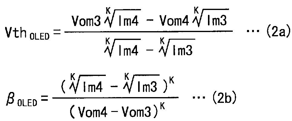
또한, 식 (2a), (2b)에 있어서, K는 2 이상 3 이하의 상수이다. 역치 전압 VthOLED는 OLED 오프셋 기억부(15c)에 기입되고, 게인 βOLED는 OLED 게인 기억부(15d)에 기입된다.In the equations (2a) and (2b), K is a constant of 2 or more and 3 or less. The threshold voltage Vth OLED is written to the OLED offset
도 6은 영상 신호 VS1에 대한 보정 처리의 플로우차트이다. 보정부(16)는 영상 신호 VS1에 포함되는 코드값 CV0에 대하여, 트랜지스터(21)의 역치 전압 VthTFT, 트랜지스터(21)의 게인 βTFT, 유기 EL 소자(24)의 역치 전압 VthOLED, 및, 유기 EL 소자(24)의 게인 βOLED를 사용하여 보정을 행한다. 이하의 처리에서 사용되는 역치 전압 VthTFT, VthOLED 및 게인 βTFT, βOLED는 보정 데이터 기억부(15)로부터 판독된 것이다.6 is a flowchart of a correction process for the video signal VS1. The
보정부(16)는, 먼저, 유기 EL 소자(24)의 발광 효율을 보정하는 처리를 행한다(스텝 S101). 구체적으로는, 보정부(16)는 다음 식 (3)에 나타내는 연산을 행함으로써, 보정 후의 코드값 CV1을 구한다.The correcting
![]()
![]()
단, 식 (3)에 있어서, γ는 화소 회로(20)마다 구한 발광 효율 보정 계수를 나타낸다. 유기 EL 소자(24)의 발광 효율이 크게 저하되어 있는 화소일수록, 발광 효율 보정 계수 γ는 큰 값을 갖는다. 또한, γ를 계산에 의해 구할 수도 있다.In Equation (3),? Represents the luminescence efficiency correction coefficient obtained for each
다음에, 보정부(16)는 보정 후의 코드값 CV1을 트랜지스터(21)의 게이트-소스간 전압을 나타내는 전압값 Vdata1TFT와 유기 EL 소자(24)의 애노드-캐소드간 전압을 나타내는 전압값 Vdata1OLED로 변환한다(스텝 S102). 스텝 S102에 있어서의 변환은, 예를 들어 미리 준비한 테이블을 참조하는 방법이나, 연산기를 사용하여 연산하는 방법에 의해 행해진다.Next, the correcting
다음에, 보정부(16)는 전압값 Vdata1TFT에 대하여 다음 식 (4)에 나타내는 연산을 행함으로써, 보정 후의 전압값 Vdata2TFT를 구한다(스텝 S103).Next, the

단, 트랜지스터(21)의 게인의 초기값의 평균값을 β0TFT로 하였을 때, 식 (4)에 포함되는 BTFT는 다음 식 (5)에 의해 제공된다.However, when the average value of the initial values of the gain of the
![]()
![]()
다음에, 보정부(16)는 전압값 Vdata1OLED에 대하여 다음 식 (6)에 나타내는 연산을 행함으로써, 보정 후의 전압값 Vdata2OLED를 구한다(스텝 S104).Next, the

단, 유기 EL 소자(24)의 게인의 초기값의 평균값을 β0OLED로 하였을 때, 식 (6)에 포함되는 BOLED는 다음 식 (7)에 의해 제공된다.However, when the average value of the initial value of the gain of the
![]()
![]()
다음에, 보정부(16)는 다음 식 (8)에 따라, 스텝 S103에서 구한 보정 후의 전압값 Vdata2TFT와, 스텝 S104에서 구한 보정 후의 전압값 Vdata2OLED를 가산한다. 이에 의해, 트랜지스터(21)의 게이트 단자에 인가되는 전압을 나타내는 전압값 Vdata가 얻어진다(스텝 S105).Next, the
![]()
![]()
마지막으로, 보정부(16)는 전압값 Vdata를 출력 코드값 CV로 변환한다(스텝 S106). 스텝 S106에 있어서의 변환은, 스텝 S102에 있어서의 변환과 마찬가지의 방법에 의해 행해진다.Finally, the
도 7은 표시 장치(10)에 있어서의 출력/측정 회로(30)와 셀렉터(41)의 대응짓기, 및, 본 측정과 더미 측정의 전환 방법을 도시하는 도면이다. 이하, 데이터선 Sj에 대응한 출력/측정 회로(30)를 j번째의 출력/측정 회로라 한다. 도 3 및 도 7에 도시한 바와 같이, 셀렉터(41)에는, 출력/측정 회로(30)가 p개씩 순서대로 대응지어진다. 예를 들어, 1번째의 셀렉터(41)에는 1∼p번째의 출력/측정 회로(30)가 대응지어지고, 2번째의 셀렉터(41)에는 (p+1)∼2p번째의 출력/측정 회로(30)가 대응지어진다. m개의 출력/측정 회로(30)는 대응하는 데이터선의 배치순에 따라서, p개씩 교대로 2개의 그룹으로 분류된다. 1∼p번째, (2p+1)∼3p번째, …의 출력/측정 회로(30)는 제1 그룹으로 분류되고, (p+1)∼2p번째, (3p+1)∼4p번째, …의 출력/측정 회로(30)는 제2 그룹으로 분류된다. 마찬가지로 (m×n)개의 화소 회로(20)는 p열씩 교대로 2개의 그룹으로 분류된다. 1∼p열째, (2p+1)∼3p열째, …의 화소 회로(20)는 제1 그룹으로 분류되고, (p+1)∼2p열째, (3p+1)∼4p열째, …의 화소 회로(20)는 제2 그룹으로 분류된다.7 is a diagram showing a correspondence between the output /
데이터선 구동/전류 측정 회로(14)는 제1 그룹 내의 화소 회로(20)에 대하여 전류 측정을 행할 때에는, 제1 그룹 내의 출력/측정 회로(30)를 사용한 본 측정과 제2 그룹 내의 출력/측정 회로(30)를 사용한 더미 측정을 동일한 타이밍에서 행하고, 본 측정의 결과와 더미 측정의 결과에 대하여 양자의 차를 구하는 연산을 행한다. 또한, 데이터선 구동/전류 측정 회로(14)는 제2 그룹 내의 화소 회로(20)에 대하여 전류 측정을 행할 때에는, 제2 그룹 내의 출력/측정 회로(30)를 사용한 본 측정과 제1 그룹 내의 출력/측정 회로(30)를 사용한 더미 측정을 동일한 타이밍에서 행하고, 본 측정의 결과와 더미 측정의 결과에 대하여 양자의 차를 구하는 연산을 행한다.When performing the current measurement for the
구체적으로는, 데이터선 구동/전류 측정 회로(14)는, 어느 프레임 기간 내에 설정된 i행째의 화소 회로(20)의 전류 측정 시의 선택 기간에서는, 1∼p번째, (2p+1)∼3p번째, …의 출력/측정 회로(30)에 측정용 전압을 공급하여 1∼p열째, (2p+1)∼3p열째, …의 화소 회로(20)에 대하여 본 측정을 행함과 함께, (p+1)∼2p번째, (3p+1)∼4p번째, …의 출력/측정 회로(30)에 제로 전압을 공급하여 (p+1)∼2p열째, (3p+1)∼4p열째, …의 화소 회로(20)에 대하여 더미 측정을 행한다(도 7의 상부를 참조). 또한, 데이터선 구동/전류 측정 회로(14)는 다른 프레임 기간 내에 설정된 i행째의 화소 회로(20)의 전류 측정 시의 선택 기간에서는, (p+1)∼2p번째, (3p+1)∼4p번째, …의 출력/측정 회로(30)에 측정용 전압을 공급하여 (p+1)∼2p열째, (3p+1)∼4p열째, …의 화소 회로(20)에 대하여 본 측정을 행함과 함께, 1∼p번째, (2p+1)∼3p번째, …의 출력/측정 회로(30)에 제로 전압을 공급하여 1∼p열째, (2p+1)∼3p열째, …의 화소 회로(20)에 대하여 더미 측정을 행한다(도 7의 하부를 참조). 어느 경우도, 본 측정과 더미 측정은 동일한 타이밍에서 행해진다.Specifically, the data line driving /
각 셀렉터(41)는 p개의 출력/측정 회로(30)의 출력 신호를, 예를 들어 오름차순으로 선택한다. 구동/측정 신호 생성 회로(17)는 k번째(단, k는 1 이상 (m/p) 이하의 홀수)의 셀렉터(41)의 출력 신호에 기초하는 디지털값과 (k+1)번째의 셀렉터(41)의 출력 신호에 기초하는 디지털값의 차를 구하고, 그 차를 일시적으로 기억한다. 이에 의해, 제1 그룹 내의 출력/측정 회로(30)를 사용한 본 측정의 결과와 제2 그룹 내의 출력/측정 회로(30)를 사용한 더미 측정의 결과의 차, 혹은, 제2 그룹 내의 출력/측정 회로(30)를 사용한 본 측정의 결과와 제1 그룹 내의 출력/측정 회로(30)를 사용한 더미 측정의 결과의 차를 구할 수 있다.Each
예를 들어, 1∼p번째의 출력/측정 회로(30)가 본 측정을 행하고, (p+1)∼2p번째의 출력/측정 회로(30)가 더미 측정을 행하는 경우, 1번째의 셀렉터(41)는 1번째의 출력/측정 회로(30)의 출력 신호, 2번째의 출력/측정 회로(30)의 출력 신호, …, p번째의 출력/측정 회로(30)의 출력 신호를 순서대로 선택한다. 이것에 맞추어, 2번째의 셀렉터(41)는 (p+1)번째의 출력/측정 회로(30)의 출력 신호, (p+2)번째의 출력/측정 회로(30)의 출력 신호, …, 2p번째의 출력/측정 회로(30)의 출력 신호를 순서대로 선택한다. 구동/측정 신호 생성 회로(17)는 1번째의 출력/측정 회로(30)의 출력 신호와 (p+1)번째의 출력/측정 회로(30)의 출력 신호의 차, 2번째의 출력/측정 회로(30)의 출력 신호와 (p+2)번째의 출력/측정 회로(30)의 출력 신호의 차, …, p번째의 출력/측정 회로(30)의 출력 신호와 2p번째의 출력/측정 회로(30)의 출력 신호의 차를 순서대로 구한다. 이에 의해, 1번째의 출력/측정 회로(30)를 사용한 본 측정의 결과와 (p+1)번째의 출력/측정 회로(30)를 사용한 더미 측정의 결과의 차, 2번째의 출력/측정 회로(30)를 사용한 본 측정의 결과와 (p+2)번째의 출력/측정 회로(30)를 사용한 더미 측정의 결과의 차, …, p번째의 출력/측정 회로(30)를 사용한 본 측정의 결과와 2p번째의 출력/측정 회로(30)를 사용한 더미 측정의 결과의 차를 구할 수 있다.For example, when the first to pth output /
더미 측정의 결과는, 화소 회로(20)를 흐르는 전류를 측정하는 회로계에서 발생하는 노이즈로 간주할 수 있다. 본 측정의 결과에는 상기 노이즈가 포함되어 있으므로, 본 측정의 결과와 더미 측정의 결과의 차를 구함으로써, 화소 회로(20)를 흐르는 전류를 노이즈를 포함시키지 않고 측정할 수 있다. i행 j열째의 화소 회로(20)에 대한 본 측정의 결과와 i행 (j+p)열째의 화소 회로(20)에 관한 더미 측정의 결과의 차는, i행 j열째의 화소 회로(20)를 흐르는 전류를 노이즈를 포함시키지 않고 측정한 결과를 나타낸다. i행 (j+p)열째의 화소 회로(20)에 대한 본 측정의 결과와 i행 j열째의 화소 회로(20)에 대한 더미 측정의 결과의 차는, i행 (j+p)열째의 화소 회로(20)를 흐르는 전류를 노이즈를 포함시키지 않고 측정한 결과를 나타낸다. 데이터선 구동/전류 측정 회로(14)는 이상에 설명한 방법에 의해 화소 회로(20)를 흐르는 전류를 측정한다.The result of the dummy measurement can be regarded as a noise generated in a circuit system for measuring the current flowing through the
이하, 본 실시 형태에 따른 표시 장치(10)의 효과를 설명한다. 화소 회로를 흐르는 전류를 측정하고, 전류 측정 결과에 기초하여 영상 신호를 보정하는 유기 EL 표시 장치에서는, 전류 측정 결과에 노이즈가 혼입되고, 그 영향을 받아 고화질 표시를 행할 수 없는 경우가 있다. 예를 들어, 전류 측정 회로에 공급되는 D/A 변환기의 출력의 불균일이나, 전류 측정 회로의 오피 앰프에 공급되는 전원 전압에 포함되는 노이즈는, 큰 노이즈의 발생 요인으로 된다. 전원 리플이나, 로드 레귤레이션, 상용 전원의 저주파 노이즈, 내부 회로로부터의 유입 노이즈 등도, 노이즈의 발생 요인으로 된다. 또한, 도 2에 도시한 출력/측정 회로(30)를 사용한 경우, 스위치 제어 신호 CLK1이 로우 레벨일 때에는, 출력/측정 회로(30)의 게인은 매우 커진다(오픈 루프 게인과 동등하게 된다). 이 때문에, 스위치 제어 신호 CLK1이 로우 레벨일 때에는, 출력/측정 회로(30)는 작은 노이즈를 크게 증폭한다.Hereinafter, the effect of the
본 실시 형태에 따른 표시 장치(10)는 본 측정과 더미 측정을 동일한 타이밍에서 행하고, 본 측정의 결과와 더미 측정의 결과에 대하여 양자의 차를 구하는 연산을 행함으로써, 화소 회로(20)를 흐르는 전류를 측정한다. 표시 장치(10)에서 각종 노이즈가 발생하였을 때, 본 측정의 결과와 더미 측정의 결과에는 동일 정도의 노이즈가 혼입된다. 이 때문에, 본 측정의 결과와 더미 측정의 결과의 차를 구함으로써, 전류 측정 시의 노이즈를 제거하여, 화소 회로(20)를 흐르는 전류를 정확하게 측정할 수 있다. 따라서, 전류 측정 결과에 기초하여 영상 신호 VS1을 보정함으로써, 전류 측정 시의 노이즈를 제거하여 고화질 표시를 행할 수 있다.The
또한, 이상의 설명에서는, 셀렉터(41)는 p개의 출력/측정 회로(30)의 출력 신호를 오름차순으로 선택하는 것으로 하였다. 이것 대신에, 셀렉터(41)는 p개의 출력/측정 회로(30)의 출력 신호를 1번째, p번째, 2번째, (p-1)번째, 3번째, (p-2)번째, …의 순서로 선택해도 된다. 혹은, 홀수번째의 셀렉터(41)는 p개의 출력/측정 회로(30)의 출력 신호를 내림차순으로 선택하고, 짝수번째의 셀렉터(41)는 p개의 출력/측정 회로(30)의 출력 신호를 오름차순으로 선택해도 된다. 이에 의해, 인접하는 출력/측정 회로(30)의 출력 신호의 사이에서 A/D 변환을 행하는 타이밍의 차를 작게 하여, 전류 측정 시의 노이즈를 효과적으로 제거할 수 있다.In the above description, the
이상에 나타내는 바와 같이, 본 실시 형태에 따른 표시 장치(10)는 복수의 주사선 GA1∼GAn, GB1∼GBn과 복수의 데이터선 S1∼Sm과 2차원 형상으로 배치된 복수의 화소 회로(20)를 포함하는 표시부(11)와, 주사선 GA1∼GAn, GB1∼GBn을 구동하는 주사선 구동 회로(13)와, 데이터선 S1∼Sm을 구동하는 데이터선 구동 회로(데이터선 구동/전류 측정 회로(14)의 일부)와, 복수의 측정부(출력/측정 회로(30))를 포함하고, 화소 회로(20)를 흐르는 전류를 측정하는 전류 측정 회로(데이터선 구동/전류 측정 회로(14)의 다른 일부)를 구비하고 있다. 전류 측정 회로는, 일부의 측정부에 측정용 신호(측정용 전압)를 공급하여 화소 회로(20)에 대하여 전류를 측정하는 본 측정과, 잔여의 측정부에 더미 신호(제로 전압)를 공급하여 전류를 측정하는 더미 측정을 동일한 타이밍에서 행하고, 본 측정의 결과와 더미 측정의 결과에 대하여 연산을 행한다. 또한, 잔여의 측정부의 적어도 일부가, 더미 측정을 행하면 된다. 이와 같이 본 측정과 더미 측정을 동일한 타이밍에서 행하고, 본 측정의 결과와 더미 측정의 결과에 대하여 연산을 행함으로써, 화소 회로(20)에 대하여 전류를 측정할 때에 측정 시의 노이즈를 제거할 수 있다. 또한, 전류 측정 결과를 사용하여, 고화질 표시를 행할 수 있다.As described above, the
또한, 전류 측정 회로는, 더미 측정을 행할 때에는 측정되어야 할 값이 대략 제로인 신호(제로 전압)를 더미 신호로서 공급하고, 본 측정의 결과와 더미 측정의 결과의 차를 구한다. 이에 의해, 화소 회로(20)에 대하여 전류를 측정할 때에 측정 시의 노이즈를 용이하게 제거할 수 있다.Further, when performing dummy measurement, a current measurement circuit supplies a signal (a zero voltage) whose value to be measured is approximately zero as a dummy signal, and obtains a difference between the result of this measurement and the result of the dummy measurement. Thereby, it is possible to easily remove the noise at the time of measurement when measuring the current with respect to the pixel circuit (20).
또한, 측정부는 데이터선 Sj에 대응하여 설치되어 있고, 전류 측정 회로는, 잔여의 측정부에 더미 신호를 공급하여 화소 회로(20)에 대하여 전류를 측정한다. 이에 의해, 더미 측정용으로 새로운 회로를 형성하지 않고, 화소 회로(20)에 대하여 전류를 측정할 때에 측정 시의 노이즈를 제거할 수 있다. 또한, 측정부는 제1 및 제2 그룹으로 분류되고, 전류 측정 회로는, 제1 기간에 있어서 제1 그룹 내의 측정부를 사용한 본 측정과 제2 그룹 내의 측정부를 사용한 더미 측정을 동일한 타이밍에서 행하고, 제2 기간에 있어서 제2 그룹 내의 측정부를 사용한 본 측정과 제1 그룹 내의 측정부를 사용한 더미 측정을 동일한 타이밍에서 행한다. 이와 같이 측정부를 2개의 그룹으로 나누고, 본 측정과 더미 측정을 교대로 행함으로써, 데이터선 S1∼Sm과 동수(m개)의 화소 회로(20)를 흐르는 전류를 2회의 본 측정에 의해 측정할 수 있다.The measuring unit is provided corresponding to the data line Sj, and the current measuring circuit supplies a dummy signal to the remaining measuring unit to measure the current with respect to the
또한, 측정부는, 대응하는 데이터선의 배치순에 따라서, 복수개(p개)씩 교대로 제1 및 제2 그룹으로 분류된다. 따라서, 화소 회로(20)에 대하여 전류를 측정할 때에, 근방의 화소 회로(20)에 대한 더미 측정 결과를 참조함으로써, 전류 측정 시의 노이즈를 효과적으로 제거할 수 있다. 또한, 전류 측정 회로는, 제1 그룹 내의 측정부의 출력에 대하여 선택을 행하는 셀렉터(홀수번째의 셀렉터(41))와, 제2 그룹 내의 측정부의 출력에 대하여 선택을 행하는 셀렉터(짝수번째의 셀렉터(41))를 포함하고 있다. 따라서, 셀렉터(41)를 사용하여 본 측정의 결과와 더미 측정의 결과를 선택하고, 선택된 2개의 측정 결과에 대하여 연산을 행할 수 있다.Further, the measuring unit is divided into the first and second groups alternately (p number) in accordance with the arrangement order of the corresponding data lines. Therefore, when measuring the current with respect to the
또한, 표시 장치(10)는 전류 측정 회로에 의해 측정된 전류에 기초하여, 데이터선 구동 회로에 공급되는 영상 신호 VS1을 보정하는 보정부(16)를 구비하고 있다. 따라서, 측정된 전류에 기초하여 영상 신호 VS1을 보정함으로써, 고화질 표시를 행할 수 있다.The
또한, 화소 회로(20)는 전기 광학 소자(유기 EL 소자(24))와, 전기 광학 소자에 직렬로 접속된 구동 트랜지스터(트랜지스터(21))와, 데이터선 Sj에 접속된 제1 도통 단자, 구동 트랜지스터의 제어 단자(게이트 단자)에 접속된 제2 도통 단자, 및, 주사선 중 제1 주사선 GAi에 접속된 제어 단자를 갖는 기입 제어 트랜지스터(트랜지스터(22))와, 데이터선 Sj에 접속된 제1 도통 단자, 구동 트랜지스터와 전기 광학 소자의 접속점에 접속된 제2 도통 단자, 및, 주사선 중 제2 주사선 GBi에 접속된 제어 단자를 갖는 판독 제어 트랜지스터(트랜지스터(23))를 포함하고 있다. 따라서, 전기 광학 소자와 구동 트랜지스터와 기입 제어 트랜지스터와 판독 제어 트랜지스터를 포함하는 화소 회로를 구비한 표시 장치에 대하여, 화소 회로에 대하여 전류를 측정할 때에 측정 시의 노이즈를 제거할 수 있다.The
또한, 표시 장치(10)는 화소 회로마다 전기 광학 소자와 구동 트랜지스터의 역치 전압과 게인을 기억하는 기억부(보정용 데이터 기억부(15))를 구비하고 있다. 보정부(16)는 전류 측정 회로에 의해 측정된 전류에 기초하여, 기억부에 기억되는 역치 전압과 게인을 구하고, 기억부에 기억된 역치 전압과 게인에 기초하여, 영상 신호 VS1을 보정한다. 따라서, 전류 측정 결과에 기초하여 전기 광학 소자와 구동 트랜지스터의 역치 전압과 게인을 구하고, 이것을 사용하여 영상 신호 VS1을 보정함으로써, 전기 광학 소자와 구동 트랜지스터의 특성의 편차나 변동을 보상하여 고화질 표시를 행할 수 있다. 또한, 데이터선 구동 회로와 전류 측정 회로는, 증폭기(오피 앰프(31))를 공유한다. 이에 의해, 표시 장치(10)의 회로량을 삭감할 수 있다The
(제2 실시 형태)(Second Embodiment)
본 발명의 제2 실시 형태에 따른 표시 장치는, 제1 실시 형태에 따른 표시 장치와 마찬가지의 구성을 갖고(도 1 및 도 2를 참조), 적, 녹 및 청의 3원색을 사용하여 화상을 표시한다. (m×n)개의 화소 회로(20)는 대응하는 데이터선마다(즉, 열마다), 적, 녹, 및, 청 중 어느 하나의 표시색을 갖는다. 1열째, 4열째, 7열째, …의 화소 회로(20)의 표시색은 적, 2열째, 5열째, 8열째, …의 화소 회로(20)의 표시색은 녹, 3열째, 6열째, 9열째, …의 화소 회로(20)의 표시색은 청이다.The display device according to the second embodiment of the present invention has the same configuration as that of the display device according to the first embodiment (see Figs. 1 and 2), and displays an image using three primary colors of red, green and blue do. (m x n)
도 8은 본 실시 형태에 따른 표시 장치에 있어서의 출력/측정 회로(30)와 셀렉터(41)의 대응짓기, 및, 본 측정과 더미 측정의 전환 방법을 도시하는 도면이다. 도 8은 도 7에 있어서 p=3으로 한 것이다. 출력/측정 회로(30)는 대응하는 데이터선의 배치순에 따라서, 3개씩 교대로 제1 및 제2 그룹으로 분류된다. 데이터선 구동/전류 측정 회로(14)는 동일한 표시색을 갖는 화소 회로(20)에 대하여 본 측정과 더미 측정을 동일한 타이밍에서 행한다.8 is a diagram showing a correspondence between the output /
이상에 나타내는 바와 같이, 본 실시 형태에 따른 표시 장치에서는, 화소 회로(20)는 대응하는 데이터선마다 복수의 표시색 중 어느 하나를 갖는다. 측정부(출력/측정 회로(30))는, 대응하는 데이터선의 배치순에 따라서, 표시색과 동수(3개)씩 교대로 제1 및 제2 그룹으로 분류된다. 이와 같이 동일한 표시색을 갖는 화소 회로(20)에 대하여 본 측정과 더미 측정을 행함으로써, 전류 측정 시의 노이즈를 효과적으로 제거할 수 있다.As described above, in the display device according to the present embodiment, the
(제3 실시 형태)(Third Embodiment)
본 발명의 제3 실시 형태에 따른 표시 장치는, 제1 실시 형태에 따른 표시 장치와 마찬가지의 구성을 갖는다(도 1 및 도 2를 참조). 본 실시 형태와 제1 실시 형태에서는, 출력/측정 회로(30)와 셀렉터(41)의 대응짓기, 및, 본 측정과 더미 측정의 전환 방법이 상이하다. 이하, 제1 실시 형태와의 상위점을 설명한다.The display device according to the third embodiment of the present invention has the same configuration as the display device according to the first embodiment (see Figs. 1 and 2). In the present embodiment and the first embodiment, the correspondence between the output /
도 9는 본 실시 형태에 따른 표시 장치에 있어서의 출력/측정 회로(30)와 셀렉터(41)의 대응짓기, 및, 본 측정과 더미 측정의 전환 방법을 도시하는 도면이다. 본 실시 형태에서는, 홀수번째의 셀렉터(41)에는 홀수번째의 출력/측정 회로(30)가 p개씩 순서대로 대응지어지고, 짝수번째의 셀렉터(41)에는 짝수번째의 출력/측정 회로(30)가 p개씩 순서대로 대응지어진다. 예를 들어, 1번째의 셀렉터(41)에는 1번째, 3번째, …, (2p-1)번째의 출력/측정 회로(30)가 대응지어지고, 2번째의 셀렉터(41)에는 2번째, 4번째, …, 2p번째의 출력/측정 회로(30)가 대응지어진다. m개의 출력/측정 회로(30)는, 대응하는 데이터선의 배치순에 따라서, 1개씩 교대로 2개의 그룹으로 분류된다. 홀수번째의 출력/측정 회로(30)는 제1 그룹으로 분류되고, 짝수번째의 출력/측정 회로(30)는 제2 그룹으로 분류된다. 마찬가지로 (m×n)개의 화소 회로(20)는 1열씩 교대로 2개의 그룹으로 분류된다. 홀수열째의 화소 회로(20)는 제1 그룹으로 분류되고, 짝수열째의 화소 회로(20)는 제2 그룹으로 분류된다.9 is a diagram showing a correspondence between the output /
데이터선 구동/전류 측정 회로(14)는 제1 그룹 내의 화소 회로(20)(홀수열째의 화소 회로(20))에 대하여 전류 측정을 행할 때에는, 제1 그룹 내의 출력/측정 회로(30)(홀수번째의 출력/측정 회로(30))를 사용한 본 측정과 제2 그룹 내의 출력/측정 회로(30)(짝수번째의 출력/측정 회로(30))를 사용한 더미 측정을 동일한 타이밍에서 행하고, 본 측정의 결과와 더미 측정의 결과의 차를 구한다. 또한, 데이터선 구동/전류 측정 회로(14)는 제2 그룹 내의 화소 회로(20)(짝수열째의 화소 회로(20))에 대하여 전류 측정을 행할 때에는, 제2 그룹 내의 출력/측정 회로(30)를 사용한 본 측정과 제1 그룹 내의 출력/측정 회로(30)를 사용한 더미 측정을 동일한 타이밍에서 행하고, 본 측정의 결과와 더미 측정의 결과의 차를 구한다.The data line driving /
구체적으로는, 데이터선 구동/전류 측정 회로(14)는 어느 프레임 기간 내에 설정된 i행째의 화소 회로(20)의 전류 측정 시의 선택 기간에서는, 1번째, 3번째, …의 출력/측정 회로(30)에 측정용 전압을 공급하여 1열째, 3열째, …의 화소 회로(20)에 대하여 본 측정을 행함과 함께, 2번째, 4번째, …의 출력/측정 회로(30)에 제로 전압을 공급하여 2열째, 4열째, …의 화소 회로(20)에 대하여 더미 측정을 행한다(도 8의 상부를 참조). 또한, 데이터선 구동/전류 측정 회로(14)는 다른 프레임 기간 내에 설정된 i행째의 화소 회로(20)의 전류 측정 시의 선택 기간에서는, 2번째, 4번째, …의 출력/측정 회로(30)에 측정용 전압을 공급하여 2열째, 4열째, …의 화소 회로(20)에 대하여 본 측정을 행함과 함께, 1번째, 3번째, …의 출력/측정 회로(30)에 제로 전압을 인가하여 1열째, 3열째, …의 화소 회로(20)에 대하여 더미 측정을 행한다(도 8의 하부를 참조). 어느 경우도, 본 측정과 더미 측정은 동일한 타이밍에서 행해진다.Specifically, in the selection period of the current measurement of the
각 셀렉터(41)는 p개의 출력/측정 회로(30)의 출력 신호를, 예를 들어 오름차순으로 선택한다. 구동/측정 신호 생성 회로(17)는 k번째(단, k는 1 이상 (m/p) 이하의 홀수)의 셀렉터(41)의 출력 신호에 기초하는 디지털값과 (k+1)번째의 셀렉터(41)의 출력 신호에 기초하는 디지털값의 차를 구하고, 그 차를 일시적으로 기억한다. 이에 의해, 홀수번째의 출력/측정 회로(30)를 사용한 본 측정의 결과와 짝수번째의 출력/측정 회로(30)를 사용한 더미 측정의 결과의 차, 혹은, 짝수번째의 출력/측정 회로(30)를 사용한 본 측정의 결과와 홀수번째의 출력/측정 회로(30)를 사용한 더미 측정의 결과의 차를 구할 수 있다. i행 j열째의 화소 회로(20)에 대한 본 측정의 결과와 i행 (j+1)열째의 화소 회로(20)에 대한 더미 측정의 결과의 차는, i행 j열째의 화소 회로(20)를 흐르는 전류를 측정한 결과를 나타낸다. i행 (j+1)열째의 화소 회로(20)에 대한 본 측정의 결과와 i행 j열째의 화소 회로(20)에 대한 더미 측정의 결과의 차는, i행 (j+1)열째의 화소 회로(20)를 흐르는 전류를 측정한 결과를 나타낸다. 데이터선 구동/전류 측정 회로(14)는 이상에 설명한 방법에 의해 화소 회로(20)를 흐르는 전류를 측정한다.Each
이상에 나타내는 바와 같이, 본 실시 형태에 따른 표시 장치에서는, 측정부(출력/측정 회로(30))는 대응하는 데이터선의 배치순에 따라서, 1개씩 교대로 제1 및 제2 그룹으로 분류된다. 따라서, 화소 회로(20)를 흐르는 전류를 측정할 때에, 인접하는 화소 회로(20)에 대한 더미 측정의 결과를 참조함으로써, 전류 측정 시의 노이즈를 효과적으로 제거할 수 있다.As described above, in the display device according to the present embodiment, the measurement section (output / measurement circuit 30) is classified into the first and second groups alternately one by one according to the arrangement order of the corresponding data line. Therefore, when the current flowing through the
(제4 실시 형태)(Fourth Embodiment)
본 발명의 제4 실시 형태에 따른 표시 장치는, 제1 실시 형태에 따른 표시 장치와 마찬가지의 구성을 갖는다(도 1 및 도 2를 참조). 단, 본 실시 형태에 따른 표시 장치는, 도 3에 도시한 데이터선 구동/전류 측정 회로(14) 대신에, 도 10에 도시한 데이터선 구동/전류 측정 회로(50)를 구비하고 있다.A display device according to a fourth embodiment of the present invention has a configuration similar to that of the display device according to the first embodiment (see Figs. 1 and 2). However, the display device according to the present embodiment is provided with the data line driving /
도 10에 도시한 데이터선 구동/전류 측정 회로(50)는 (m+m/p)개의 출력/측정 회로(30), 신호 변환 회로(51) 및 구동/측정 신호 생성 회로(52)를 포함하고 있다. 신호 변환 회로(51)는 (m/p)개의 셀렉터(53), (2m/p)개의 오프셋 회로(54) 및 (2m/p)개의 A/D 변환기(55)를 포함하고 있다.The data line driving /
(m+m/p)개의 출력/측정 회로(30)는 m개의 본 측정용 회로(이하, 출력/측정 회로(30a)라 함)와, (m/p)개의 더미 측정용 회로(이하, 출력/측정 회로(30b)라 함)로 분류된다. m개의 출력/측정 회로(30a)는, 각각, m개의 데이터선 S1∼Sm에 접속된다. 데이터선 Sj에 접속된 출력/측정 회로(30a) 내의 오피 앰프(31)의 비반전 입력 단자에는, 데이터선 Sj에 대응한 D/A 변환기(도시하지 않음)의 출력 신호 DVj가 인가된다. m개의 출력/측정 회로(30a)와 (m/p)개의 셀렉터(53)는 제1 실시 형태와 동일한 형태로 접속된다.(m / p) number of output / measurement circuits 30 (hereinafter, referred to as output /
(m/p)개의 출력/측정 회로(30b)는, 각각, 표시부(11)에 형성된 (m/p)개의 더미 배선 D1∼Dm/p에 접속된다. 더미 배선 D1∼Dm/p는, 데이터선 S1∼Sm과 동일한 부하를 갖고, 더미 측정 대상 회로로서 기능한다. 출력/측정 회로(30b) 내의 오피 앰프(31)의 비반전 입력 단자에는, 제로 전압 DVzero가 고정적으로 인가된다.(m / p) number of output /
셀렉터(53)는 p개의 출력/측정 회로(30a)의 출력 신호 중으로부터 1개의 아날로그 신호를 선택한다. 오프셋 회로(54)는 셀렉터(53)에 의해 선택된 아날로그 신호, 또는, 출력/측정 회로(30b)의 출력 신호에 대하여 소정의 오프셋을 가산한다. A/D 변환기(55)는 오프셋 회로(54)로부터 출력된 아날로그 신호를 디지털값으로 변환한다.The
구동/측정 신호 생성 회로(52)는 각 A/D 변환기(55)에 의해 구한 디지털값에 기초하여, 본 측정의 결과와 더미 측정의 결과의 차를 구하여 일시적으로 기억한다. 셀렉터(53)는 p개의 출력/측정 회로(30a)의 출력 신호를 순서대로 선택한다. 셀렉터(53)가 p회의 선택을 완료하였을 때, 구동/측정 신호 생성 회로(52)에는, 본 측정에 의한 결과와 더미 측정에 의한 결과의 차를 나타내는 m개의 디지털값이 기억되어 있다. 구동/측정 신호 생성 회로(52)는 표시 제어 회로(12)에 대하여, m개의 디지털값을 포함하는 모니터 신호 MS를 출력한다.The drive / measurement
도 11은 본 실시 형태에 따른 표시 장치에 있어서의 본 측정과 더미 측정의 타이밍을 도시하는 도면이다. 도 11에는 데이터선 S1∼Sp에 접속된 출력/측정 회로(30a)에 의한 본 측정과, 더미 배선 D1에 접속된 출력/측정 회로(30b)에 의한 더미 측정의 타이밍이 기재되어 있다. 여기에서는, 본 측정과 더미 측정을, 측정과 A/D 변환으로 나누어 생각한다.11 is a diagram showing the timing of this measurement and the dummy measurement in the display device according to the present embodiment. 11 shows the main measurement by the output /
도 11에 도시한 바와 같이, 시각 t0에서는, 더미 배선 D1에 접속된 출력/측정 회로(30b)에 의한 측정과, 데이터선 S1∼Sp에 접속된 출력/측정 회로(30a)에 의한 측정이 동일한 타이밍에서 행해진다. 시각 t1에서는, 더미 배선 D1에 접속된 출력/측정 회로(30b)의 출력 신호에 대한 A/D 변환과, 데이터선 S1에 접속된 출력/측정 회로(30a)의 출력 신호에 대한 A/D 변환이 동일한 타이밍에서 행해진다. 시각 t2에서는, 더미 배선 D1에 접속된 출력/측정 회로(30b)의 출력 신호에 대한 A/D 변환과, 데이터선 S2에 접속된 출력/측정 회로(30a)의 출력 신호에 대한 A/D 변환이 동일한 타이밍에서 행해진다. 마찬가지로, 시각 t3∼tp에서는, 더미 배선 D1에 접속된 출력/측정 회로(30b)의 출력 신호에 대한 A/D 변환과, 데이터선 S3∼Sp에 접속된 출력/측정 회로(30a)의 출력 신호에 대한 A/D 변환이 동일한 타이밍에서 행해진다. 이와 같이 본 측정의 결과에 대한 A/D 변환과 더미 측정의 결과에 대한 A/D 변환을 동일한 타이밍에서 행함으로써, 전류 측정 시의 노이즈를 효과적으로 제거할 수 있다.11, at time t0, the measurement by the output /
또한, 이상의 설명에서는, 더미 배선의 개수는 (m/p)개인 것으로 하였지만, 더미 배선의 수는 1개 이상이면 임의여도 된다. 예를 들어, 더미 배선이 1개인 경우에는, 데이터선 구동/전류 측정 회로는 도 12에 도시한 구성을 갖는다. 또한, 더미 측정 대상 회로로서, 더미 배선 이외의 회로를 사용해도 된다.In the above description, the number of dummy wirings is (m / p), but the number of dummy wirings may be one or more. For example, when there is one dummy wiring, the data line driving / current measuring circuit has the configuration shown in Fig. As the dummy measurement target circuit, a circuit other than the dummy wiring may be used.
이상에 나타내는 바와 같이, 본 실시 형태에 따른 표시 장치는, 1개 이상의 더미 측정 대상 회로(더미 배선 D1∼Dm/p)를 구비하고 있다. 일부의 측정부(출력/측정 회로(30a))는 데이터선 S1∼Sm에 대응하여 설치되고, 잔여의 측정부(출력/측정 회로(30b))는 더미 측정 대상 회로에 대응하여 설치된다. 전류 측정 회로(데이터선 구동/전류 측정 회로(50)의 일부)는 잔여의 측정부에 더미 신호(제로 전압)를 공급하여 더미 측정 대상 회로를 흐르는 전류를 측정한다. 이와 같이 더미 측정 대상 회로를 설치하고, 더미 측정 대상 회로를 흐르는 전류를 측정하는 더미 측정을 행함으로써, 데이터선과 동수(m개)의 화소 회로(20)를 흐르는 전류를 1회의 본 측정에 의해 측정할 수 있다. 또한, 데이터선 S1∼Sm과 동일한 부하를 갖는 더미 측정 대상 회로를 사용함으로써, 본 측정과 동일한 조건에서 더미 측정을 행할 수 있다. 또한, 전류 측정 회로는, 일부의 측정부의 출력에 대하여 선택을 행하는 셀렉터(53)를 포함하고 있다. 따라서, 셀렉터(53)를 사용하여 본 측정의 결과를 선택하고, 선택된 본 측정의 결과와 더미 측정의 결과 사이에서 연산을 행할 수 있다.As described above, the display device according to the present embodiment has one or more dummy measurement target circuits (dummy wirings D1 to Dm / p). Some of the measurement units (output /
또한, 전류 측정 회로는, 화소 회로(20)에 대하여 전류를 측정한 결과를 나타내는 아날로그 신호를 디지털값으로 변환하는 A/D 변환기(55)를 포함하고, 본 측정의 결과에 대한 A/D 변환과 더미 측정의 결과에 대한 A/D 변환을 동일한 타이밍에서 행한다. 이에 의해, 전류 측정 시의 노이즈를 효과적으로 제거할 수 있다.The current measuring circuit includes an A /
(제5 실시 형태)(Fifth Embodiment)
제1∼제4 실시 형태에서는, 화소 회로에 대하여 전류를 측정하는 전류 측정 회로를 구비한 표시 장치에 대하여 설명하였다. 제5 실시 형태에서는, 화소 회로에 대하여 전압을 측정하는 전압 측정 회로를 구비한 표시 장치에 대하여 설명한다.In the first to fourth embodiments, the display device provided with the current measuring circuit for measuring the current with respect to the pixel circuit has been described. In the fifth embodiment, a display device provided with a voltage measuring circuit for measuring a voltage with respect to a pixel circuit will be described.
도 13은 본 발명의 제5 실시 형태에 따른 표시 장치의 구성을 도시하는 블록도이다. 도 13에 도시한 표시 장치(60)는 제1 실시 형태에 따른 표시 장치(10)(도 1)에 있어서, 데이터선 구동/전류 측정 회로(14)를 데이터선 구동/전압 측정 회로(데이터선 구동 회로와 전압 측정 회로의 겸용 회로)(61)로 치환한 것이다. 데이터선 구동/전압 측정 회로(61)는 구동/측정 신호 생성 회로(17), 신호 변환 회로(40) 및 m개의 출력/측정 회로(62)를 포함하고 있다.13 is a block diagram showing a configuration of a display device according to a fifth embodiment of the present invention. The
도 14는 화소 회로(20)와 출력/측정 회로(62)의 구성을 도시하는 도면이다. 도 14에는 i행 j열째의 화소 회로(20)와, 데이터선 Sj에 대응한 출력/측정 회로(62)가 기재되어 있다. 화소 회로(20)의 구성은 제1 실시 형태와 동일하다. 이하, 트랜지스터(21)의 소스 단자와 유기 EL 소자(24)의 애노드 단자가 접속된 절점을 N1이라 한다.Fig. 14 is a diagram showing the configuration of the
출력/측정 회로(62)는 전압 생성 회로(63), 전류원(64), 전압 측정 회로(65) 및 스위치(66)를 포함하고 있다. 스위치(66)의 일단은, 데이터선 Sj에 접속된다. 스위치(66)는 스위치 제어 신호 SC에 따라서, 데이터선 Sj를 전압 생성 회로(63)에 접속할지, 전류원(64)과 전압 측정 회로(65)에 접속할지를 전환한다.The output /
전압 생성 회로(63)는 신호 변환 회로(40)로부터 출력된 디지털 데이터에 기초하여 데이터 전압을 출력하거나, 레퍼런스 전압을 출력한다. 데이터선 Sj가 전압 생성 회로(63)에 접속되어 있을 때, 전압 생성 회로(63)로부터 출력된 데이터 전압 또는 레퍼런스 전압은 데이터선 Sj에 인가된다. 데이터선 Sj가 전류원(64)과 전압 측정 회로(65)에 접속되어 있을 때, 전류원(64)은 데이터선 Sj에 대하여 소정량의 전류를 흘리고, 전압 측정 회로(65)는 그때의 데이터선 Sj의 전압을 측정한다.The
영상 신호 VS1을 보정하여 영상 신호 VS2를 구하기 위해, 데이터선 구동/전압 측정 회로(61)는 각 화소 회로(20)에 대하여 4종류의 전압을 측정한다. 보다 상세하게는, 각 화소 회로(20) 내의 트랜지스터(21)의 특성을 구하기 위해, 데이터선 구동/전압 측정 회로(61)는 화소 회로(20)에 트랜지스터(21)가 온하는 레퍼런스 전압을 기입하고, 전류원(64)으로부터 제1 측정용 전류 In1을 흘렸을 때의 절점 N1의 전압 Vn1과, 화소 회로(20)에 트랜지스터(21)가 온하는 전압을 기입하고, 전류원(64)으로부터 제2 측정용 전류 In2(>In1)를 흘렸을 때의 절점 N1의 전압 Vn2와, 화소 회로(20)에 트랜지스터(21)가 오프하는 전압을 기입하고, 전류원(64)으로부터 제3 측정용 전류 In3을 흘렸을 때의 절점 N1의 전압 Vn3과, 화소 회로(20)에 트랜지스터(21)가 오프하는 전압을 기입하고, 전류원(64)으로부터 제4 측정용 전류 In4(>In3)을 흘렸을 때의 절점 N1의 전압 Vn4를 측정한다.In order to correct the video signal VS1 to obtain the video signal VS2, the data line driving /
주사선 구동 회로(13)와 데이터선 구동/전압 측정 회로(61)는 1행분의 화소 회로(20)에 대한 기입 처리와, 1행분의 화소 회로(20)에 대하여 4종류의 전압 Vn1∼Vn4 중 어느 하나를 측정하는 처리를 행한다. 예를 들어, 주사선 구동 회로(13)와 데이터선 구동/전압 측정 회로(61)는 연속한 4프레임 기간 중, 제1∼제4 프레임 기간 내의 i번째의 라인 기간에서는 i행째의 화소 회로(20)에 대하여 전압 Vn1∼Vn4를 각각 측정하고, 그 이외의 라인 기간에서는 1행분의 화소 회로(20)에 대한 기입 처리를 행해도 된다.The scanning
보정부(16)는 측정된 4종류의 전압 Vn1∼Vn4에 기초하여, 트랜지스터(21)와 유기 EL 소자(24)의 특성을 구하는 처리를 행하고, 구한 2종류의 특성에 기초하여 영상 신호 VS1을 보정한다. 보다 상세하게는, 보정부(16)는 2종류의 전압 Vn1, Vn2에 기초하여, 트랜지스터(21)의 특성으로서 역치 전압과 게인을 구하고, 2종류의 전압 Vn3, Vn4에 기초하여, 유기 EL 소자(24)의 특성으로서 역치 전압과 게인을 구한다. 트랜지스터(21)의 역치 전압과 게인 및 유기 EL 소자(24)의 역치 전압과 게인을 구하는 방법은, 제1 실시 형태와 마찬가지이다. 보정부(16)는 구한 역치 전압과 게인을 보정 데이터 기억부(15)에 기입하고, 보정 데이터 기억부(15)로부터 판독한 역치 전압과 게인을 사용하여 영상 신호 VS1을 보정한다.The
이상에 나타내는 바와 같이, 본 실시 형태에 따른 표시 장치(60)는 측정 회로로서 전류 측정 회로 대신에, 화소 회로(20) 내의 절점 N1의 전압 Vn1∼Vn4를 측정하는 전압 측정 회로(65)를 구비하고, 전압 측정 회로(65)에 의해 측정된 전압 Vn1∼Vn4에 기초하여, 데이터선 구동 회로(데이터선 구동/전압 측정 회로(61)의 일부)에 공급되는 영상 신호 VS1에 대하여 보정을 행하는 보정부(16)를 구비하고 있다.As described above, the
본 실시 형태에 따른 표시 장치(60)에 의하면, 제1 실시 형태에 따른 표시 장치(10)와 마찬가지로, 본 측정과 더미 측정을 동일한 타이밍에서 행하고, 본 측정의 결과와 더미 측정의 결과에 대하여 연산을 행함으로써, 화소 회로(20) 내의 절점 N1의 전압을 측정할 때에 측정 시의 노이즈를 제거할 수 있다. 또한, 전압 측정 결과를 사용하여, 고화질 표시를 행할 수 있다.According to the
또한, 이상에 설명한 각 실시 형태에 따른 표시 장치는 화소 회로(20)와 출력/측정 회로(30)를 구비하는 것으로 하였지만, 표시 장치는 다른 화소 회로를 구비하고 있어도 되고, 다른 출력/측정 회로를 구비하고 있어도 된다.Although the display device according to each of the embodiments described above is provided with the
이상에 나타내는 바와 같이, 본 발명의 표시 장치에 의하면, 본 측정과 더미 측정을 동일한 타이밍에서 행하고, 본 측정의 결과와 더미 측정의 결과의 차를 구함으로써, 화소 회로에 대하여 전류 또는 전압을 측정할 때에 측정 시의 노이즈를 제거할 수 있다. 또한, 전류 또는 전압의 측정 결과를 사용하여, 고화질 표시를 행할 수 있다.As described above, according to the display device of the present invention, the current measurement or the dummy measurement is performed at the same timing, and the difference between the result of this measurement and the result of the dummy measurement is determined, Noise at the time of measurement can be removed. In addition, high-quality display can be performed using measurement results of current or voltage.
본 발명의 표시 장치는, 화소 회로에 대하여 전류 또는 전압을 측정할 때에 측정 시의 노이즈를 제거할 수 있다는 특징을 가지므로, 유기 EL 표시 장치 등, 전기 광학 소자를 포함하는 화소 회로를 구비한 각종 표시 장치에 이용할 수 있다.The display device of the present invention is characterized by being capable of removing noise at the time of measurement when measuring a current or a voltage with respect to the pixel circuit. Therefore, the display device of the present invention can be applied to various types of display devices including a pixel circuit including an electro- And can be used for a display device.
10, 60 : 표시 장치
11 : 표시부
12 : 표시 제어 회로
13 : 주사선 구동 회로
14, 50 : 데이터선 구동/전류 측정 회로
15 : 보정 데이터 기억부
16 : 보정부
17, 52 : 구동/측정 신호 생성 회로
20 : 화소 회로
21 : 트랜지스터(구동 트랜지스터)
22 : 트랜지스터(기입 제어 트랜지스터)
23 : 트랜지스터(판독 제어 트랜지스터)
24 : 유기 EL 소자(전기 광학 소자)
25, 32 : 콘덴서
30, 62 : 출력/측정 회로
31 : 오피 앰프
33∼35, 66 : 스위치
40, 51 : 신호 변환 회로
41, 53 : 셀렉터
42, 54 : 오프셋 회로
43, 55 : A/D 변환기
61 : 데이터선 구동/전압 측정 회로
63 : 전압 생성 회로
64 : 전류원
65 : 전압 측정 회로
GA1∼GAn, GB1∼GBn : 주사선
S1∼Sm : 데이터선10, 60: display device
11:
12: Display control circuit
13: scanning line driving circuit
14, 50: Data line driving / current measuring circuit
15: correction data storage section
16:
17, 52: drive / measurement signal generation circuit
20:
21: transistor (driving transistor)
22: transistor (write control transistor)
23: transistor (read control transistor)
24: Organic EL element (electro-optical element)
25, 32: Capacitors
30, 62: output / measurement circuit
31: Op Amp
33 to 35, 66:
40, 51: Signal conversion circuit
41, 53: selector
42, 54: offset circuit
43, 55: A / D converter
61: Data line driving / voltage measuring circuit
63: voltage generating circuit
64: current source
65: Voltage measuring circuit
GA1 to GAn, GB1 to GBn:
S1 to Sm: Data lines
Claims (20)
복수의 주사선과 복수의 데이터선과 2차원 형상으로 배치된 복수의 화소 회로를 포함하는 표시부와,
상기 주사선을 구동하는 주사선 구동 회로와,
상기 데이터선을 구동하는 데이터선 구동 회로와,
복수의 측정부를 포함하고, 상기 화소 회로에 대하여 전류 또는 전압을 측정하는 측정 회로를 구비하고,
상기 측정 회로는, 일부의 측정부에 측정용 신호를 공급하여 상기 화소 회로에 대하여 전류 또는 전압을 측정하는 본 측정과, 잔여의 측정부의 적어도 일부에 더미 신호를 공급하여 전류 또는 전압을 측정하는 더미 측정을 동일한 타이밍에서 행하고, 상기 본 측정의 결과와 상기 더미 측정의 결과에 대하여 연산을 행하고,
상기 측정 회로는, 상기 더미 측정을 행할 때에는 측정되어야 할 값이 제로인 신호를 상기 더미 신호로서 공급하고, 상기 본 측정의 결과와 상기 더미 측정의 결과의 차를 구하고,
상기 측정부는 상기 데이터선에 대응하여 설치되어 있고,
상기 측정 회로는, 상기 잔여의 측정부의 적어도 일부에 상기 더미 신호를 공급하여 상기 화소 회로에 대하여 전류 또는 전압을 측정하고,
상기 측정부는 제1 및 제2 그룹으로 분류되고,
상기 측정 회로는, 제1 기간에 있어서 상기 제1 그룹 내의 측정부를 사용한 본 측정과 상기 제2 그룹 내의 측정부를 사용한 더미 측정을 동일한 타이밍에서 행하고, 제2 기간에 있어서 상기 제2 그룹 내의 측정부를 사용한 본 측정과 상기 제1 그룹 내의 측정부를 사용한 더미 측정을 동일한 타이밍에서 행하고,
상기 측정부는, 대응하는 데이터선의 배치순에 따라서, 복수개씩 교대로 상기 제1 및 제2 그룹으로 분류되는 것을 특징으로 하는 표시 장치.As an active matrix type display device,
A display section including a plurality of scanning lines, a plurality of data lines, and a plurality of pixel circuits arranged in a two-dimensional shape;
A scanning line driving circuit for driving the scanning line,
A data line driving circuit for driving the data line,
And a measuring circuit for measuring a current or a voltage with respect to the pixel circuit,
The measurement circuit includes a main measurement circuit for supplying a measurement signal to a part of the measurement unit to measure a current or a voltage with respect to the pixel circuit and a dummy signal supply unit for supplying a dummy signal to at least a part of the remaining measurement unit, Measurement is performed at the same timing, arithmetic operation is performed on the result of the main measurement and the result of the dummy measurement,
Wherein the measurement circuit supplies a signal having a value of zero to be measured as the dummy signal when the dummy measurement is performed to obtain a difference between the result of the main measurement and the result of the dummy measurement,
Wherein the measuring unit is provided corresponding to the data line,
Wherein the measurement circuit supplies the dummy signal to at least a part of the remaining measurement unit to measure a current or a voltage with respect to the pixel circuit,
The measuring unit is classified into first and second groups,
Wherein the measurement circuit performs the main measurement using the measurement unit in the first group and the dummy measurement using the measurement unit in the second group at the same timing in the first period and the measurement using the measurement unit in the second group The present measurement and the dummy measurement using the measurement unit in the first group are performed at the same timing,
Wherein the measuring unit is divided into a first group and a second group alternately by a plurality in accordance with the arrangement order of the corresponding data line.
복수의 주사선과 복수의 데이터선과 2차원 형상으로 배치된 복수의 화소 회로를 포함하는 표시부와,
상기 주사선을 구동하는 주사선 구동 회로와,
상기 데이터선을 구동하는 데이터선 구동 회로와,
복수의 측정부를 포함하고, 상기 화소 회로에 대하여 전류 또는 전압을 측정하는 측정 회로를 구비하고,
상기 측정 회로는, 일부의 측정부에 측정용 신호를 공급하여 상기 화소 회로에 대하여 전류 또는 전압을 측정하는 본 측정과, 잔여의 측정부의 적어도 일부에 더미 신호를 공급하여 전류 또는 전압을 측정하는 더미 측정을 동일한 타이밍에서 행하고, 상기 본 측정의 결과와 상기 더미 측정의 결과에 대하여 연산을 행하고,
상기 측정 회로는, 상기 더미 측정을 행할 때에는 측정되어야 할 값이 제로인 신호를 상기 더미 신호로서 공급하고, 상기 본 측정의 결과와 상기 더미 측정의 결과의 차를 구하고,
상기 측정부는 상기 데이터선에 대응하여 설치되어 있고,
상기 측정 회로는, 상기 잔여의 측정부의 적어도 일부에 상기 더미 신호를 공급하여 상기 화소 회로에 대하여 전류 또는 전압을 측정하고,
상기 측정부는 제1 및 제2 그룹으로 분류되고,
상기 측정 회로는, 제1 기간에 있어서 상기 제1 그룹 내의 측정부를 사용한 본 측정과 상기 제2 그룹 내의 측정부를 사용한 더미 측정을 동일한 타이밍에서 행하고, 제2 기간에 있어서 상기 제2 그룹 내의 측정부를 사용한 본 측정과 상기 제1 그룹 내의 측정부를 사용한 더미 측정을 동일한 타이밍에서 행하고,
상기 측정부는, 대응하는 데이터선의 배치순에 따라서, 1개씩 교대로 상기 제1 및 제2 그룹으로 분류되는 것을 특징으로 하는 표시 장치.As an active matrix type display device,
A display section including a plurality of scanning lines, a plurality of data lines, and a plurality of pixel circuits arranged in a two-dimensional shape;
A scanning line driving circuit for driving the scanning line,
A data line driving circuit for driving the data line,
And a measuring circuit for measuring a current or a voltage with respect to the pixel circuit,
The measurement circuit includes a main measurement circuit for supplying a measurement signal to a part of the measurement unit to measure a current or a voltage with respect to the pixel circuit and a dummy signal supply unit for supplying a dummy signal to at least a part of the remaining measurement unit, Measurement is performed at the same timing, arithmetic operation is performed on the result of the main measurement and the result of the dummy measurement,
Wherein the measurement circuit supplies a signal having a value of zero to be measured as the dummy signal when the dummy measurement is performed to obtain a difference between the result of the main measurement and the result of the dummy measurement,
Wherein the measuring unit is provided corresponding to the data line,
Wherein the measurement circuit supplies the dummy signal to at least a part of the remaining measurement unit to measure a current or a voltage with respect to the pixel circuit,
The measuring unit is classified into first and second groups,
Wherein the measurement circuit performs the main measurement using the measurement unit in the first group and the dummy measurement using the measurement unit in the second group at the same timing in the first period and the measurement using the measurement unit in the second group The present measurement and the dummy measurement using the measurement unit in the first group are performed at the same timing,
Wherein the measuring unit is divided into the first and second groups alternately one by one according to the arrangement order of the corresponding data line.
복수의 주사선과 복수의 데이터선과 2차원 형상으로 배치된 복수의 화소 회로를 포함하는 표시부와,
상기 주사선을 구동하는 주사선 구동 회로와,
상기 데이터선을 구동하는 데이터선 구동 회로와,
복수의 측정부를 포함하고, 상기 화소 회로에 대하여 전류 또는 전압을 측정하는 측정 회로를 구비하고,
상기 측정 회로는, 일부의 측정부에 측정용 신호를 공급하여 상기 화소 회로에 대하여 전류 또는 전압을 측정하는 본 측정과, 잔여의 측정부의 적어도 일부에 더미 신호를 공급하여 전류 또는 전압을 측정하는 더미 측정을 동일한 타이밍에서 행하고, 상기 본 측정의 결과와 상기 더미 측정의 결과에 대하여 연산을 행하고,
상기 측정 회로는, 상기 더미 측정을 행할 때에는 측정되어야 할 값이 제로인 신호를 상기 더미 신호로서 공급하고, 상기 본 측정의 결과와 상기 더미 측정의 결과의 차를 구하고,
상기 측정부는 상기 데이터선에 대응하여 설치되어 있고,
상기 측정 회로는, 상기 잔여의 측정부의 적어도 일부에 상기 더미 신호를 공급하여 상기 화소 회로에 대하여 전류 또는 전압을 측정하고,
상기 측정부는 제1 및 제2 그룹으로 분류되고,
상기 측정 회로는, 제1 기간에 있어서 상기 제1 그룹 내의 측정부를 사용한 본 측정과 상기 제2 그룹 내의 측정부를 사용한 더미 측정을 동일한 타이밍에서 행하고, 제2 기간에 있어서 상기 제2 그룹 내의 측정부를 사용한 본 측정과 상기 제1 그룹 내의 측정부를 사용한 더미 측정을 동일한 타이밍에서 행하고,
상기 측정 회로는, 상기 제1 그룹 내의 측정부의 출력에 대하여 선택을 행하는 셀렉터와, 상기 제2 그룹 내의 측정부의 출력에 대하여 선택을 행하는 셀렉터를 더 포함하는 것을 특징으로 하는 표시 장치.As an active matrix type display device,
A display section including a plurality of scanning lines, a plurality of data lines, and a plurality of pixel circuits arranged in a two-dimensional shape;
A scanning line driving circuit for driving the scanning line,
A data line driving circuit for driving the data line,
And a measuring circuit for measuring a current or a voltage with respect to the pixel circuit,
The measurement circuit includes a main measurement circuit for supplying a measurement signal to a part of the measurement unit to measure a current or a voltage with respect to the pixel circuit and a dummy signal supply unit for supplying a dummy signal to at least a part of the remaining measurement unit, Measurement is performed at the same timing, arithmetic operation is performed on the result of the main measurement and the result of the dummy measurement,
Wherein the measurement circuit supplies a signal having a value of zero to be measured as the dummy signal when the dummy measurement is performed to obtain a difference between the result of the main measurement and the result of the dummy measurement,
Wherein the measuring unit is provided corresponding to the data line,
Wherein the measurement circuit supplies the dummy signal to at least a part of the remaining measurement unit to measure a current or a voltage with respect to the pixel circuit,
The measuring unit is classified into first and second groups,
Wherein the measurement circuit performs the main measurement using the measurement unit in the first group and the dummy measurement using the measurement unit in the second group at the same timing in the first period and the measurement using the measurement unit in the second group The present measurement and the dummy measurement using the measurement unit in the first group are performed at the same timing,
Wherein the measurement circuit further includes a selector for selecting an output of the measurement unit in the first group and a selector for selecting the output of the measurement unit in the second group.
상기 화소 회로는, 대응하는 데이터선마다 복수의 표시색 중 어느 하나를 갖고,
상기 측정부는, 대응하는 데이터선의 배치순에 따라서, 상기 표시색과 동수씩 교대로 상기 제1 및 제2 그룹으로 분류되는 것을 특징으로 하는 표시 장치.6. The method of claim 5,
Wherein the pixel circuit has any one of a plurality of display colors for each corresponding data line,
Wherein the measuring section is divided into the first and second groups alternately in the order of arrangement of the corresponding data line, the number being the same as the display color.
1개 이상의 더미 측정 대상 회로를 더 구비하고,
상기 일부의 측정부는 상기 데이터선에 대응하여 설치되고, 상기 잔여의 측정부는 상기 더미 측정 대상 회로에 대응하여 설치되어 있고,
상기 측정 회로는, 상기 잔여의 측정부의 적어도 일부에 상기 더미 신호를 공급하여 상기 더미 측정 대상 회로에 대하여 전류 또는 전압을 측정하는 것을 특징으로 하는 표시 장치.8. The method according to any one of claims 5 to 7,
Further comprising at least one dummy measurement target circuit,
Wherein the part of the measuring part is provided corresponding to the data line and the remaining measuring part is provided corresponding to the dummy measuring object circuit,
Wherein the measurement circuit supplies the dummy signal to at least a part of the remaining measurement unit and measures a current or voltage with respect to the dummy measurement target circuit.
상기 더미 측정 대상 회로는, 상기 데이터선과 동일한 부하를 갖는 것을 특징으로 하는 표시 장치.10. The method of claim 9,
Wherein the dummy measurement object circuit has the same load as the data line.
상기 측정 회로는, 상기 일부의 측정부의 출력에 대하여 선택을 행하는 셀렉터를 더 포함하는 것을 특징으로 하는 표시 장치.10. The method of claim 9,
Wherein the measuring circuit further comprises a selector for selecting an output of the part of the measuring unit.
상기 측정 회로에서 측정된 전류 또는 전압에 기초하여, 상기 데이터선 구동 회로에 공급되는 영상 신호를 보정하는 보정부를 더 구비한 표시 장치.8. The method according to any one of claims 5 to 7,
And a correction section for correcting the video signal supplied to the data line driving circuit based on the current or voltage measured by the measuring circuit.
상기 화소 회로는, 전기 광학 소자와, 상기 전기 광학 소자에 직렬로 접속된 구동 트랜지스터를 포함하는 것을 특징으로 하는 표시 장치.8. The method according to any one of claims 5 to 7,
Wherein the pixel circuit includes an electro-optical element and a driving transistor connected in series to the electro-optical element.
상기 측정 회로에서 측정된 전류 또는 전압에 기초하여, 상기 데이터선 구동 회로에 공급되는 영상 신호를 보정하는 보정부와,
상기 화소 회로마다 상기 전기 광학 소자와 상기 구동 트랜지스터의 역치 전압과 게인을 기억하는 기억부를 더 구비하고,
상기 보정부는, 상기 측정 회로에 의해 측정된 전류 또는 전압에 기초하여, 상기 기억부에 기억되는 역치 전압과 게인을 구하고, 상기 기억부에 기억된 역치 전압과 게인에 기초하여 상기 영상 신호를 보정하는 것을 특징으로 하는 표시 장치.14. The method of claim 13,
A correcting unit for correcting a video signal supplied to the data line driving circuit based on the current or voltage measured by the measuring circuit,
And a storage section for storing a threshold voltage and a gain of the electro-optical element and the driving transistor for each of the pixel circuits,
Wherein the correction section obtains a threshold voltage and a gain stored in the storage section based on the current or voltage measured by the measurement circuit and corrects the video signal based on the threshold voltage and gain stored in the storage section And the display device.
상기 화소 회로는,
상기 데이터선에 접속된 제1 도통 단자, 상기 구동 트랜지스터의 제어 단자에 접속된 제2 도통 단자, 및, 상기 주사선 중 제1 주사선에 접속된 제어 단자를 갖는 기입 제어 트랜지스터와,
상기 데이터선에 접속된 제1 도통 단자, 상기 구동 트랜지스터와 상기 전기 광학 소자의 접속점에 접속된 제2 도통 단자, 및, 상기 주사선 중 제2 주사선에 접속된 제어 단자를 갖는 판독 제어 트랜지스터를 더 포함하는 것을 특징으로 하는 표시 장치.14. The method of claim 13,
The pixel circuit includes:
A write control transistor having a first conduction terminal connected to the data line, a second conduction terminal connected to a control terminal of the drive transistor, and a control terminal connected to the first one of the scan lines,
And a read control transistor having a first conduction terminal connected to the data line, a second conduction terminal connected to the connection point of the driving transistor and the electro-optical element, and a control terminal connected to the second one of the scanning lines And the display device.
상기 측정 회로는, 상기 화소 회로에 대하여 전류 또는 전압을 측정한 결과를 나타내는 아날로그 신호를 디지털값으로 변환하는 A/D 변환기를 더 포함하고, 상기 본 측정의 결과에 대한 A/D 변환과 상기 더미 측정의 결과에 대한 A/D 변환을 동일한 타이밍에서 행하는 것을 특징으로 하는 표시 장치.8. The method according to any one of claims 5 to 7,
Wherein the measuring circuit further comprises an A / D converter for converting an analog signal representing a result of measuring a current or voltage to the pixel circuit into a digital value, wherein the A / D conversion and the dummy And the A / D conversion of the result of the measurement is performed at the same timing.
상기 측정 회로는, 상기 화소 회로를 흐르는 전류를 측정하는 전류 측정 회로인 것을 특징으로 하는 표시 장치.8. The method according to any one of claims 5 to 7,
Wherein the measuring circuit is a current measuring circuit for measuring a current flowing through the pixel circuit.
상기 데이터선 구동 회로와 상기 전류 측정 회로는, 증폭 회로를 공유하는 것을 특징으로 하는 표시 장치.18. The method of claim 17,
Wherein the data line driving circuit and the current measuring circuit share an amplifying circuit.
상기 측정 회로는, 상기 화소 회로 내의 절점의 전압을 측정하는 전압 측정 회로인 것을 특징으로 하는 표시 장치.8. The method according to any one of claims 5 to 7,
Wherein the measuring circuit is a voltage measuring circuit for measuring a voltage at a node in the pixel circuit.
Applications Claiming Priority (3)
| Application Number | Priority Date | Filing Date | Title |
|---|---|---|---|
| JPJP-P-2015-019160 | 2015-02-03 | ||
| JP2015019160 | 2015-02-03 | ||
| PCT/JP2016/052238 WO2016125641A1 (en) | 2015-02-03 | 2016-01-27 | Display device and drive method |
Publications (2)
| Publication Number | Publication Date |
|---|---|
| KR20170104512A KR20170104512A (en) | 2017-09-15 |
| KR101978587B1 true KR101978587B1 (en) | 2019-05-14 |
Family
ID=56563991
Family Applications (1)
| Application Number | Title | Priority Date | Filing Date |
|---|---|---|---|
| KR1020177021175A Expired - Fee Related KR101978587B1 (en) | 2015-02-03 | 2016-01-27 | Display device and driving method thereof |
Country Status (4)
| Country | Link |
|---|---|
| US (1) | US10510285B2 (en) |
| KR (1) | KR101978587B1 (en) |
| CN (1) | CN107210022B (en) |
| WO (1) | WO2016125641A1 (en) |
Families Citing this family (7)
| Publication number | Priority date | Publication date | Assignee | Title |
|---|---|---|---|---|
| CN107980159B (en) | 2016-12-27 | 2021-06-29 | 深圳市柔宇科技股份有限公司 | Pixel circuit driving method, pixel circuit group, and organic light-emitting display device |
| US11663973B1 (en) * | 2018-05-10 | 2023-05-30 | Apple Inc. | External compensation for displays using sensing and emission differences |
| US10818208B2 (en) * | 2018-09-14 | 2020-10-27 | Novatek Microelectronics Corp. | Source driver |
| KR102560747B1 (en) * | 2018-12-20 | 2023-07-27 | 엘지디스플레이 주식회사 | Organic Light Emitting Display Device And Pixel Sensing Method Of The Same |
| KR102773250B1 (en) | 2020-05-22 | 2025-02-28 | 삼성디스플레이 주식회사 | Display device |
| JP7688965B2 (en) * | 2020-07-22 | 2025-06-05 | 武漢天馬微電子有限公司 | display device |
| CN113611250A (en) * | 2021-08-10 | 2021-11-05 | 京东方科技集团股份有限公司 | Display substrate and display device |
Citations (6)
| Publication number | Priority date | Publication date | Assignee | Title |
|---|---|---|---|---|
| JP2003195813A (en) | 2001-09-07 | 2003-07-09 | Semiconductor Energy Lab Co Ltd | Light emitting device |
| JP2004004675A (en) | 2002-03-29 | 2004-01-08 | Seiko Epson Corp | Electronic device, method of driving electronic device, electro-optical device, and electronic apparatus |
| JP2007085782A (en) | 2005-09-20 | 2007-04-05 | Agilent Technol Inc | Pixel drive current measuring method and apparatus |
| JP2008250069A (en) | 2007-03-30 | 2008-10-16 | Sanyo Electric Co Ltd | Electroluminescence display device |
| JP2010281874A (en) | 2009-06-02 | 2010-12-16 | Casio Computer Co Ltd | LIGHT EMITTING DEVICE, ITS DRIVE CONTROL METHOD, AND ELECTRONIC DEVICE |
| JP2011164135A (en) | 2010-02-04 | 2011-08-25 | Global Oled Technology Llc | Display device |
Family Cites Families (7)
| Publication number | Priority date | Publication date | Assignee | Title |
|---|---|---|---|---|
| JP2001195026A (en) * | 2000-01-14 | 2001-07-19 | Victor Co Of Japan Ltd | Matrix type display device |
| JP4266682B2 (en) * | 2002-03-29 | 2009-05-20 | セイコーエプソン株式会社 | Electronic device, driving method of electronic device, electro-optical device, and electronic apparatus |
| JP4909587B2 (en) * | 2005-12-28 | 2012-04-04 | Necディスプレイソリューションズ株式会社 | Image display device |
| JP2008299019A (en) * | 2007-05-30 | 2008-12-11 | Sony Corp | Cathode potential control device, self-luminous display device, electronic device, and cathode potential control method |
| US8139007B2 (en) | 2008-03-31 | 2012-03-20 | Casio Computer Co., Ltd. | Light-emitting device, display device, and method for controlling driving of the light-emitting device |
| JP4877261B2 (en) | 2008-03-31 | 2012-02-15 | カシオ計算機株式会社 | Display device and drive control method thereof |
| KR102005052B1 (en) | 2012-12-03 | 2019-07-31 | 삼성디스플레이 주식회사 | Error Compensation part and Organic Light Emitting Display Device Using the same |
-
2016
- 2016-01-27 KR KR1020177021175A patent/KR101978587B1/en not_active Expired - Fee Related
- 2016-01-27 CN CN201680006453.2A patent/CN107210022B/en not_active Expired - Fee Related
- 2016-01-27 US US15/548,237 patent/US10510285B2/en active Active
- 2016-01-27 WO PCT/JP2016/052238 patent/WO2016125641A1/en not_active Ceased
Patent Citations (6)
| Publication number | Priority date | Publication date | Assignee | Title |
|---|---|---|---|---|
| JP2003195813A (en) | 2001-09-07 | 2003-07-09 | Semiconductor Energy Lab Co Ltd | Light emitting device |
| JP2004004675A (en) | 2002-03-29 | 2004-01-08 | Seiko Epson Corp | Electronic device, method of driving electronic device, electro-optical device, and electronic apparatus |
| JP2007085782A (en) | 2005-09-20 | 2007-04-05 | Agilent Technol Inc | Pixel drive current measuring method and apparatus |
| JP2008250069A (en) | 2007-03-30 | 2008-10-16 | Sanyo Electric Co Ltd | Electroluminescence display device |
| JP2010281874A (en) | 2009-06-02 | 2010-12-16 | Casio Computer Co Ltd | LIGHT EMITTING DEVICE, ITS DRIVE CONTROL METHOD, AND ELECTRONIC DEVICE |
| JP2011164135A (en) | 2010-02-04 | 2011-08-25 | Global Oled Technology Llc | Display device |
Also Published As
| Publication number | Publication date |
|---|---|
| CN107210022A (en) | 2017-09-26 |
| US10510285B2 (en) | 2019-12-17 |
| CN107210022B (en) | 2020-12-15 |
| WO2016125641A1 (en) | 2016-08-11 |
| US20170365205A1 (en) | 2017-12-21 |
| KR20170104512A (en) | 2017-09-15 |
Similar Documents
| Publication | Publication Date | Title |
|---|---|---|
| KR101978587B1 (en) | Display device and driving method thereof | |
| US9847056B2 (en) | Picture signal processing circuit, picture signal processing method, and display unit | |
| JP6284636B2 (en) | Display device and driving method thereof | |
| CN107863071B (en) | Organic Light Emitting Display Device | |
| JP5240538B2 (en) | Display driving device and driving method thereof, and display device and driving method thereof | |
| US9171503B2 (en) | Organic light emitting display, method for driving the same, and method for manufacturing the same | |
| KR102702446B1 (en) | Display device and methode of driving the same | |
| KR102356368B1 (en) | Orgainic light emitting display and driving method for the same | |
| US9361823B2 (en) | Display device | |
| US20190012948A1 (en) | Pixel circuit, and display device and driving method therefor | |
| KR101322322B1 (en) | Light emitting device and drive control method thereof, and electronic device | |
| US10141020B2 (en) | Display device and drive method for same | |
| WO2016129463A1 (en) | Display device and method for driving same | |
| JP2009180765A (en) | Display driving device, display device and driving method thereof | |
| US9852682B2 (en) | Organic light-emitting display configured to correct image data and method of driving the same | |
| JPWO2014021201A1 (en) | Display device and driving method thereof | |
| WO2016158481A1 (en) | Display device and drive method for same | |
| JP2008039799A (en) | Display device and drive control method thereof | |
| KR101939231B1 (en) | Organic light emitting diode display device and method of measuring pixel current of the same | |
| JP2008185809A (en) | Image display device and driving method thereof | |
| KR101843020B1 (en) | Light emitting diode display | |
| CN111402798B (en) | Pixel driving circuit, control method thereof and display device | |
| JP4284704B2 (en) | Display drive device and drive control method thereof, and display device and drive control method thereof | |
| WO2017026335A1 (en) | Display device and method for driving same | |
| JP6677402B2 (en) | Image display device, image display control device, and image display method |
Legal Events
| Date | Code | Title | Description |
|---|---|---|---|
| A201 | Request for examination | ||
| P11-X000 | Amendment of application requested |
St.27 status event code: A-2-2-P10-P11-nap-X000 |
|
| P13-X000 | Application amended |
St.27 status event code: A-2-2-P10-P13-nap-X000 |
|
| PA0105 | International application |
St.27 status event code: A-0-1-A10-A15-nap-PA0105 |
|
| PA0201 | Request for examination |
St.27 status event code: A-1-2-D10-D11-exm-PA0201 |
|
| PG1501 | Laying open of application |
St.27 status event code: A-1-1-Q10-Q12-nap-PG1501 |
|
| E902 | Notification of reason for refusal | ||
| PE0902 | Notice of grounds for rejection |
St.27 status event code: A-1-2-D10-D21-exm-PE0902 |
|
| E13-X000 | Pre-grant limitation requested |
St.27 status event code: A-2-3-E10-E13-lim-X000 |
|
| P11-X000 | Amendment of application requested |
St.27 status event code: A-2-2-P10-P11-nap-X000 |
|
| P13-X000 | Application amended |
St.27 status event code: A-2-2-P10-P13-nap-X000 |
|
| E701 | Decision to grant or registration of patent right | ||
| PE0701 | Decision of registration |
St.27 status event code: A-1-2-D10-D22-exm-PE0701 |
|
| GRNT | Written decision to grant | ||
| PR0701 | Registration of establishment |
St.27 status event code: A-2-4-F10-F11-exm-PR0701 |
|
| PR1002 | Payment of registration fee |
St.27 status event code: A-2-2-U10-U12-oth-PR1002 Fee payment year number: 1 |
|
| PG1601 | Publication of registration |
St.27 status event code: A-4-4-Q10-Q13-nap-PG1601 |
|
| PR1001 | Payment of annual fee |
St.27 status event code: A-4-4-U10-U11-oth-PR1001 Fee payment year number: 4 |
|
| PR1001 | Payment of annual fee |
St.27 status event code: A-4-4-U10-U11-oth-PR1001 Fee payment year number: 5 |
|
| PC1903 | Unpaid annual fee |
St.27 status event code: A-4-4-U10-U13-oth-PC1903 Not in force date: 20240509 Payment event data comment text: Termination Category : DEFAULT_OF_REGISTRATION_FEE |
|
| PC1903 | Unpaid annual fee |
St.27 status event code: N-4-6-H10-H13-oth-PC1903 Ip right cessation event data comment text: Termination Category : DEFAULT_OF_REGISTRATION_FEE Not in force date: 20240509 |