KR101973395B1 - Light emitting module - Google Patents
Light emitting module Download PDFInfo
- Publication number
- KR101973395B1 KR101973395B1 KR1020120087167A KR20120087167A KR101973395B1 KR 101973395 B1 KR101973395 B1 KR 101973395B1 KR 1020120087167 A KR1020120087167 A KR 1020120087167A KR 20120087167 A KR20120087167 A KR 20120087167A KR 101973395 B1 KR101973395 B1 KR 101973395B1
- Authority
- KR
- South Korea
- Prior art keywords
- light emitting
- ceramic substrate
- heat dissipation
- hole
- disposed
- Prior art date
- Legal status (The legal status is an assumption and is not a legal conclusion. Google has not performed a legal analysis and makes no representation as to the accuracy of the status listed.)
- Expired - Fee Related
Links
Images


Classifications
-
- H—ELECTRICITY
- H10—SEMICONDUCTOR DEVICES; ELECTRIC SOLID-STATE DEVICES NOT OTHERWISE PROVIDED FOR
- H10H—INORGANIC LIGHT-EMITTING SEMICONDUCTOR DEVICES HAVING POTENTIAL BARRIERS
- H10H20/00—Individual inorganic light-emitting semiconductor devices having potential barriers, e.g. light-emitting diodes [LED]
- H10H20/80—Constructional details
- H10H20/85—Packages
- H10H20/858—Means for heat extraction or cooling
- H10H20/8582—Means for heat extraction or cooling characterised by their shape
-
- F—MECHANICAL ENGINEERING; LIGHTING; HEATING; WEAPONS; BLASTING
- F21—LIGHTING
- F21V—FUNCTIONAL FEATURES OR DETAILS OF LIGHTING DEVICES OR SYSTEMS THEREOF; STRUCTURAL COMBINATIONS OF LIGHTING DEVICES WITH OTHER ARTICLES, NOT OTHERWISE PROVIDED FOR
- F21V29/00—Protecting lighting devices from thermal damage; Cooling or heating arrangements specially adapted for lighting devices or systems
- F21V29/50—Cooling arrangements
- F21V29/502—Cooling arrangements characterised by the adaptation for cooling of specific components
- F21V29/503—Cooling arrangements characterised by the adaptation for cooling of specific components of light sources
-
- F—MECHANICAL ENGINEERING; LIGHTING; HEATING; WEAPONS; BLASTING
- F21—LIGHTING
- F21V—FUNCTIONAL FEATURES OR DETAILS OF LIGHTING DEVICES OR SYSTEMS THEREOF; STRUCTURAL COMBINATIONS OF LIGHTING DEVICES WITH OTHER ARTICLES, NOT OTHERWISE PROVIDED FOR
- F21V19/00—Fastening of light sources or lamp holders
- F21V19/001—Fastening of light sources or lamp holders the light sources being semiconductors devices, e.g. LEDs
-
- F—MECHANICAL ENGINEERING; LIGHTING; HEATING; WEAPONS; BLASTING
- F21—LIGHTING
- F21V—FUNCTIONAL FEATURES OR DETAILS OF LIGHTING DEVICES OR SYSTEMS THEREOF; STRUCTURAL COMBINATIONS OF LIGHTING DEVICES WITH OTHER ARTICLES, NOT OTHERWISE PROVIDED FOR
- F21V29/00—Protecting lighting devices from thermal damage; Cooling or heating arrangements specially adapted for lighting devices or systems
- F21V29/50—Cooling arrangements
- F21V29/70—Cooling arrangements characterised by passive heat-dissipating elements, e.g. heat-sinks
- F21V29/83—Cooling arrangements characterised by passive heat-dissipating elements, e.g. heat-sinks the elements having apertures, ducts or channels, e.g. heat radiation holes
-
- H—ELECTRICITY
- H10—SEMICONDUCTOR DEVICES; ELECTRIC SOLID-STATE DEVICES NOT OTHERWISE PROVIDED FOR
- H10H—INORGANIC LIGHT-EMITTING SEMICONDUCTOR DEVICES HAVING POTENTIAL BARRIERS
- H10H20/00—Individual inorganic light-emitting semiconductor devices having potential barriers, e.g. light-emitting diodes [LED]
- H10H20/80—Constructional details
- H10H20/85—Packages
- H10H20/855—Optical field-shaping means, e.g. lenses
-
- H—ELECTRICITY
- H10—SEMICONDUCTOR DEVICES; ELECTRIC SOLID-STATE DEVICES NOT OTHERWISE PROVIDED FOR
- H10H—INORGANIC LIGHT-EMITTING SEMICONDUCTOR DEVICES HAVING POTENTIAL BARRIERS
- H10H20/00—Individual inorganic light-emitting semiconductor devices having potential barriers, e.g. light-emitting diodes [LED]
- H10H20/80—Constructional details
- H10H20/85—Packages
- H10H20/8506—Containers
Landscapes
- Engineering & Computer Science (AREA)
- General Engineering & Computer Science (AREA)
- Led Device Packages (AREA)
Abstract
실시 예는 발광 모듈에 관한 것으로, 광손실을 최소화하여 광출력을 향상시킬 수 있고, 유테틱 본딩(Eutectic Bonding)을 사용하여 공정 차별화를 구현할 수 있고, 고 방열 및 장 수명을 구현할 수 있다. 그리고, 범용 설계가 가능하며, 콤팩트(compact) 설계를 통해 소형화가 가능하다. 또한, 개면 박리에 의한 변색, 변질을 방지할 수 있고, 외부의 수분이나 공기가 내부로 침투하지 못하도록 구조를 개선할 수 있으며, 제조 공정 및 비용을 줄일 수 있다.
실시 예의 발광 모듈은, 상면과 하면을 포함하고,상면과 하면을 관통하는 관통 홀을 가지는 세라믹 기판, 세라믹 기판의 관통 홀에 배치되는 방열 블록, 세라믹 기판 상에 배치되며 캐비티를 형성하는 측벽을 갖는 몸체, 캐비티 내부의 방열 블록 상에 배치되는 발광 칩, 몸체 상에 배치되며 관통 홀을 갖는 캡, 캡의 관통 홀에 배치되는 투명 창, 세라믹 기판의 상면과 방열 블록의 상면을 직접적으로 접촉하며, 방열 블록의 상면 전체를 덮도록 배치된 제1 돌출방지층 및 세라믹 기판의 하면과 방열 블록의 하면을 직접적으로 접촉하며, 방열 블록의 하면 전체를 덮도록 배치된 제2 돌출방지층을 포함하고, 세라믹 기판의 상면에서의 세라믹 기판의 관통 홀의 최대 폭은, 세라믹 기판의 하면에서의 세라믹 기판의 관통 홀의 최대 폭보다 작고, 방열 블록은 제2 돌출방지층에 접하는 면이 제1 돌출방지층에 접하는 면보다 더 넓어 지도록 단차를 이루고, 투명 창의 하면과 발광 칩의 상면 사이의 간격은 0.1 mm 이상 0.3 mm 이하이고, 발광 칩의 폭은 방열 블록의 폭보다 작고, 제1 돌출방지층과 제2 돌출방지층과 세라믹 기판의 폭은 동일하고, 제1 돌출방지층과 제2 돌출방지층과 방열 블록의 두께의 합은 0.2mm 이상 0.6mm 이하이고, 캡은 관통 홀을 정의하는 단차면을 포함하고, 단차면에 투명 창이 배치되고, 캡의 관통 홀은 상부 직경이 하부 직경보다 더 작고, 투명 창은 단차면과 대응되는 단차면을 포함하며 투명 창의 상면은 캡의 상면보다 낮을 수 있다.Embodiments relate to a light emitting module, which can minimize optical loss and improve light output, can realize process differentiation using eutectic bonding, and can achieve high heat dissipation and long service life. And it can be general-purpose design, and it can be downsized by compact design. In addition, it is possible to prevent discoloration and deterioration due to delamination on the front surface, to improve the structure so that external moisture and air can not penetrate into the interior, and manufacturing process and cost can be reduced.
The light emitting module of the embodiment includes a ceramic substrate including an upper surface and a lower surface and having a through hole penetrating the upper surface and the lower surface, a heat dissipation block disposed in the through hole of the ceramic substrate, a sidewall formed on the ceramic substrate and having a cavity A cap having a through hole disposed on the body, a transparent window disposed in the through hole of the cap, a top surface of the ceramic substrate directly contacting the top surface of the heat dissipation block, A first protrusion preventing layer disposed so as to cover the entire upper surface of the heat dissipation block and a second protrusion preventing layer directly contacting the lower surface of the heat dissipation block and the lower surface of the ceramic substrate and covering the entire lower surface of the heat dissipation block, The maximum width of the through hole of the ceramic substrate on the upper surface of the ceramic substrate is smaller than the maximum width of the through hole of the ceramic substrate on the lower surface of the ceramic substrate, 2 protrusion preventing layer is larger than a surface contacting the first protrusion preventing layer, the distance between the lower surface of the transparent window and the upper surface of the light emitting chip is 0.1 mm or more and 0.3 mm or less, and the width of the light emitting chip is the width The total thickness of the first and second protrusion preventing layers and the heat dissipation block is equal to or greater than 0.2 mm and equal to or less than 0.6 mm, Wherein the transparent window is disposed in the stepped surface, the through hole of the cap has a lower diameter smaller than the lower diameter, the transparent window includes a stepped surface corresponding to the stepped surface, and the upper surface of the transparent window has a stepped surface May be lower than the upper surface.
Description
실시 예는 발광 모듈에 관한 것이다.
An embodiment relates to a light emitting module.
반도체의 3-5족 또는 2-6족 화합물 반도체 물질을 이용한 발광 다이오드(Light Emitting Diode)나 레이저 다이오드와 같은 발광소자는 박막 성장 기술 및 소자 재료의 개발로 적색, 녹색, 청색 및 자외선 등 다양한 색을 구현할 수 있으며, 형광 물질을 이용하거나 색을 조합함으로써 효율이 좋은 백색 광선도 구현이 가능하며, 형광등, 백열등 등 기존의 광원에 비해 저소비 전력, 반영구적인 수명, 빠른 응답속도, 안전성, 환경친화성의 장점을 가진다.BACKGROUND ART Light emitting devices such as light emitting diodes and laser diodes using semiconductor materials of Group 3-5 or 2-6 group semiconductors have been widely used for various colors such as red, green, blue, and ultraviolet And it is possible to realize white light rays with high efficiency by using fluorescent materials or colors, and it is possible to realize low energy consumption, semi-permanent life time, quick response speed, safety and environment friendliness compared to conventional light sources such as fluorescent lamps and incandescent lamps .
따라서, 광 통신 수단의 송신 모듈, LCD(Liquid Crystal Display) 표시 장치의 백라이트를 구성하는 냉 음극관(CCFL: Cold Cathode Fluorescence Lamp)을 대체하는 발광 다이오드 백라이트, 형광등이나 백열 전구를 대체할 수 있는 백색 발광 다이오드 조명 장치, 자동차 헤드 라이트 및 신호등에까지 응용이 확대되고 있다.Therefore, a transmission module of the optical communication means, a light emitting diode backlight replacing a cold cathode fluorescent lamp (CCFL) constituting a backlight of an LCD (Liquid Crystal Display) display device, a white light emitting element capable of replacing a fluorescent lamp or an incandescent lamp Diode lighting, automotive headlights, and traffic lights.
메탈기판에 자외선(UV) LED를 실장한 발광 모듈의 경우, 자외선 반사광이 메탈기판 상의 절연층에 닿아 절연층에 포함된 유기 재질이 변색되거나 변질되어 발광 모듈의 광 출력 저하를 유발하여 신뢰성이 저하되는 문제점이 존재한다. 따라서 메탈기판과 같은 우수한 방열 특성을 유지하면서도 발광 모듈의 신뢰성 향상과 전 반사 효율이 좋은 무기 재질을 사용할 필요가 있다.
In the case of a light emitting module in which an ultraviolet (UV) LED is mounted on a metal substrate, since the ultraviolet reflected light touches the insulating layer on the metal substrate, the organic material contained in the insulating layer is discolored or deteriorated, . Therefore, it is necessary to use an inorganic material having improved reliability of the light emitting module and excellent antireflection efficiency while maintaining excellent heat radiation characteristics as the metal substrate.
전술한 문제점을 해결하기 위하여 실시 예가 이루고자 하는 기술적 과제는, 광손실을 최소화하여 광출력을 향상시킬 수 있는 발광 모듈을 제시하는 데 있다.SUMMARY OF THE INVENTION The present invention has been made in view of the above problems, and it is an object of the present invention to provide a light emitting module capable of improving light output by minimizing light loss.
또한, 실시 예가 이루고자 하는 다른 기술적 과제는, 유테틱 본딩(Eutectic Bonding)을 사용하여 공정 차별화를 구현할 수 있는 발광 모듈을 제시하는 데 있다.Another embodiment of the present invention is to provide a light emitting module capable of implementing process differentiation using eutectic bonding.
또한, 실시 예가 이루고자 하는 또 다른 기술적 과제는, 고 방열 및 장 수명을 구현할 수 있는 발광 모듈을 제시하는 데 있다.It is another object of the present invention to provide a light emitting module capable of realizing high heat dissipation and long service life.
또한, 실시 예가 이루고자 하는 또 다른 기술적 과제는, 280nm, 365nm, 385nm, 395nm, 405nm 를 동일한 패키지로 구현할 수 있어 범용 설계가 가능한 발광 모듈을 제시하는 데 있다.Another embodiment of the present invention is to provide a light emitting module capable of implementing 280nm, 365nm, 385nm, 395nm, and 405nm in the same package, and capable of general designing.
또한, 실시 예가 이루고자 하는 또 다른 기술적 과제는, 콤팩트(compact) 설계를 통해 소형화가 가능한 발광 모듈을 제시하는 데 있다.It is another object of the present invention to provide a light emitting module that can be miniaturized through a compact design.
또한, 실시 예가 이루고자 하는 또 다른 기술적 과제는, 개면 박리에 의한 변색, 변질을 방지할 수 있는 발광 모듈을 제시하는 데 있다.It is another object of the present invention to provide a light emitting module capable of preventing discoloration and deterioration due to separation on the front surface.
또한, 실시 예가 이루고자 하는 또 다른 기술적 과제는, 외부의 수분이나 공기가 내부로 침투하지 못하도록 구조를 개선한 발광 모듈을 제시하는 데 있다.Another embodiment of the present invention is to provide a light emitting module which is improved in structure so that external moisture or air can not penetrate into the interior.
또한, 실시 예가 이루고자 하는 또 다른 기술적 과제는, 제조 공정 및 비용을 줄일 수 있는 발광 모듈을 제시하는 데 있다.
It is another object of the present invention to provide a light emitting module capable of reducing the manufacturing process and cost.
본 발명의 해결과제는 이상에서 언급된 것들에 한정되지 않으며, 언급되지 아니한 다른 해결과제들은 아래의 기재로부터 당업자에게 명확하게 이해되어 질 수 있을 것이다.
The solution to the problem of the present invention is not limited to those mentioned above, and other solutions not mentioned can be clearly understood by those skilled in the art from the following description.
전술한 기술적 과제를 해결하기 위한 수단으로서, 실시 예의 발광 모듈은, 상면과 하면을 포함하고, 상기 상면과 상기 하면을 관통하는 관통 홀을 가지는 세라믹 기판, 상기 관통 홀에 배치되는 방열 블록, 상기 세라믹 기판 상에 배치되며 캐비티를 형성하는 측벽을 갖는 몸체, 상기 캐비티 내부의 상기 방열 블록 상에 배치되는 발광 칩, 상기 몸체 상에 배치되며 관통 홀을 갖는 캡, 상기 캡의 관통 홀에 배치되는 투명 창, 상기 세라믹 기판의 상면과 상기 방열 블록의 상면을 직접적으로 접촉하며, 상기 방열 블록의 상면 전체를 덮도록 배치된 제1 돌출방지층 및 상기 세라믹 기판의 하면과 상기 방열 블록의 하면을 직접적으로 접촉하며, 상기 방열 블록의 하면 전체를 덮도록 배치된 제2 돌출방지층을 포함하고, 상기 세라믹 기판의 상면에서의 상기 세라믹 기판의 관통 홀의 최대 폭은, 상기 세라믹 기판의 하면에서의 상기 세라믹 기판의 관통 홀의 최대 폭보다 작고, 상기 방열 블록은 상기 제2 돌출방지층에 접하는 면이 상기 제1 돌출방지층에 접하는 면보다 더 넓어 지도록 단차를 이루고, 상기 투명 창의 하면과 상기 발광 칩의 상면 사이의 간격은 0.1 mm 이상 0.3 mm 이하이고, 상기 발광 칩의 폭은 상기 방열 블록의 폭보다 작고, 상기 제1 돌출방지층과 상기 제2 돌출방지층과 상기 세라믹 기판의 폭은 동일하고, 상기 제1 돌출방지층과 상기 제2 돌출방지층과 상기 방열 블록의 두께의 합은 0.2mm 이상 0.6mm 이하이고, 상기 캡은 상기 관통 홀을 정의하는 단차면을 포함하고, 상기 단차면에 상기 투명 창이 배치되고, 상기 관통 홀은 상부 직경이 하부 직경보다 더 작고, 상기 투명 창은 상기 단차면과 대응되는 단차면을 포함하며 상기 투명 창의 상면은 상기 캡의 상면보다 낮을 수 있다.As a means for solving the above-mentioned technical problems, a light emitting module of an embodiment includes a ceramic substrate including an upper surface and a lower surface and having a through hole penetrating the upper surface and the lower surface, a heat dissipation block disposed in the through hole, A light emitting chip disposed on the heat dissipation block inside the cavity, a cap disposed on the body and having a through hole, a transparent window disposed on the through hole of the cap, , A first protrusion preventing layer directly contacting the upper surface of the ceramic substrate and the upper surface of the heat dissipation block and covering the entire upper surface of the heat dissipation block and the lower surface of the ceramic substrate directly contacting the lower surface of the heat dissipation block And a second protrusion preventing layer disposed so as to cover the entire lower surface of the heat dissipation block, wherein the upper surface of the ceramic substrate The maximum width of the through hole of the ceramic substrate is smaller than the maximum width of the through hole of the ceramic substrate on the lower surface of the ceramic substrate and the surface in contact with the second protrusion preventing layer is wider than the surface contacting the first protrusion preventing layer Wherein a distance between the lower surface of the transparent window and the upper surface of the light emitting chip is 0.1 mm or more and 0.3 mm or less and the width of the light emitting chip is smaller than the width of the heat blocking block, The total thickness of the first protrusion preventing layer, the second protrusion preventing layer, and the heat dissipation block is 0.2 mm or more and 0.6 mm or less, and the cap has a step of defining the through hole Wherein the transparent window is disposed on the stepped surface, the through hole has an upper diameter smaller than a lower diameter, and the transparent window corresponds to the stepped surface Including the step surface and the upper surface of the transparent window may be lower than an upper surface of the cap.
상기 발광 모듈은, 상기 발광 칩과 상기 방열 블록 사이에 배치된서브마운트를 더 포함할 수 있다.The light emitting module may further include a submount disposed between the light emitting chip and the heat dissipation block.
상기 캡은 단차면을 가지며, 상기 단차면에 상기 투명 창이 배치될 수 있다.The cap has a stepped surface, and the transparent window may be disposed on the stepped surface.
상기 캡의 관통 홀은 상부 직경이 하부 직경보다 더 크고, 상기 투명 창은 상기 단차면과 대응되는 단차를 가질 수 있다. The through hole of the cap may have an upper diameter larger than a lower diameter, and the transparent window may have a step corresponding to the stepped surface.
상기 캡의 관통 홀은 상부 직경이 하부 직경보다 더 작고, 상기 투명 창은 상기 단차면과 대응되는 단차를 가질 수 있다. The through hole of the cap may have an upper diameter smaller than a lower diameter, and the transparent window may have a step corresponding to the stepped surface.
상기 캡과 상기 몸체는, 진공 상태 또는 질소(N2) 가스에서 Au-Sn 유테틱(Eutectic) 본딩으로 결합될 수 있다.The cap and the body may be bonded by Au-Sn eutectic bonding in a vacuum state or a nitrogen (N 2 ) gas.
상기 몸체의 측벽은 수직면, 경사면, 계단형 중 어느 하나의 형상을 가질 수 있다.The side wall of the body may have any one of a vertical surface, an inclined surface, and a stepped surface.
상기 발광 칩은 플립칩으로 본딩될 수 있다. 또한, 상기 발광 칩은 Au 페이스트를 이용한 본딩 또는 Au-Sn 유테틱(Eutectic) 본딩으로 고정될 수 있다.The light emitting chip may be bonded to the flip chip. The light emitting chip may be fixed by bonding using Au paste or Au-Sn eutectic bonding.
상기 발광 칩과 상기 투명 창 사이의 간격은 0.2mm 이상 0.3㎜ 이하일 수 있다.The distance between the light emitting chip and the transparent window may be 0.2 mm or more and 0.3 mm or less.
상기 세라믹 기판 및 상기 몸체는, 고온 동시 소성 세라믹(high temperature co-fired ceramic: HTCC) 또는 저온 동시 소성 세라믹(Low Temperature Cofired Ceramics: LTCC)으로 이루어질 수 있다.The ceramic substrate and the body may be formed of a high temperature co-fired ceramic (HTCC) or a low temperature cofired ceramic (LTCC).
상기 세라믹 기판 및 상기 몸체는, SiO2, SixOy, Si3Ny, SiOxNy, Al2O3, AlN 중 어느 하나를 포함할 수 있다.The ceramic substrate and the body may include any one of SiO 2 , Si x O y , Si 3 N y , SiO x N y , Al 2 O 3 , and AlN.
상기 방열 블록은 Cu, M, W, Ag, Mo, CuMo, CuW 중 어느 하나를 포함할 수 있다.The heat dissipation block may include any one of Cu, M, W, Ag, Mo, CuMo and CuW.
상기 투명 창은 SiO2(Quartz, UV Fused Silica), Al2O3(Sapphire), LiF, MgF2, CaF2, Low Iron Transparent Glass, B2O3를 포함한 글라스 재질 중 어느 하나로 이루어질 수 있다.The transparent window may be made of any one of glass materials including SiO 2 (Quartz, UV Fused Silica), Al 2 O 3 (Sapphire), LiF, MgF 2 , CaF 2 , Low Iron Transparent Glass and B 2 O 3 .
상기 캐비티는 진공 상태이거나, 질소(N2) 가스 또는 포밍 가스(forming gas)가 충진될 수 있다.The cavity may be in a vacuum state, or may be filled with nitrogen (N 2 ) gas or forming gas.
상기 발광 칩을 포위하도록 상기 캐비티 내에 형성되는 몰딩부를 더 포함할 수 있다.And a molding part formed in the cavity to surround the light emitting chip.
상기 몰딩부는, 형광체가 혼합된 고 굴절률 또는 저 굴절률 Si계 Resin 또는 하이브리드계 Resin 중 적어도 하나를 포함할 수 있다.The molding part may include at least one of a high refractive index or a low refractive index Si-based resin mixed with a fluorescent material or a hybrid system resin.
상기 세라믹 기판은 회로 패턴을 포함하고, 상기 회로 패턴과 상기 발광 칩이 전기적으로 연결될 수 있다.The ceramic substrate may include a circuit pattern, and the circuit pattern and the light emitting chip may be electrically connected.
상기 세라믹 기판의 하부에 방열 패드를 더 포함할 수 있다.The ceramic substrate may further include a heat radiating pad at a lower portion thereof.
상기 발광 칩은, 200nm 이상 405㎚ 이하의 파장을 갖는 심 자외선(Deep UV) LED 칩 또는 근 자외선(Near UV) LED 칩을 포함할 수 있다.The light emitting chip may include a deep UV LED chip or a near UV LED chip having a wavelength of 200 nm or more and 405 nm or less.
상기 세라믹 기판은 상기 발광 칩이 위치하는 공간과 분리된 위치에 제너다이오드가 탑재될 수 있다.
The zener diode may be mounted on the ceramic substrate at a position separated from a space where the light emitting chip is located.
실시 예에 따르면, 광손실을 최소화하여 광출력을 향상시킬 수 있다.According to the embodiment, the light output can be improved by minimizing the light loss.
또한, 유테틱 본딩(Eutectic Bonding)을 사용하여 공정 차별화를 구현할 수 있고, 고 방열 및 장 수명을 구현할 수 있다.In addition, it is possible to realize process differentiation by using eutectic bonding and realize high heat dissipation and long service life.
또한, 280nm, 365nm, 385nm, 395nm, 405nm 를 동일한 패키지로 구현할 수 있어 범용 설계가 가능하며, 콤팩트(compact) 설계를 통해 소형화가 가능하다.In addition, 280nm, 365nm, 385nm, 395nm, and 405nm can be implemented in the same package, making it possible to design for general use, and compactness through compact design.
또한, 개면 박리에 의한 변색, 변질을 방지할 수 있다.Further, it is possible to prevent discoloration and deterioration due to separation on the front surface.
또한, 외부의 수분이나 공기가 내부로 침투하지 못하도록 구조를 개선할 수 있으며, 제조 공정 및 비용을 줄일 수 있다.
Further, the structure can be improved so that external moisture or air can not penetrate into the interior, and manufacturing process and cost can be reduced.
본 발명의 효과는 이상에서 언급된 것들에 한정되지 않으며, 언급되지 아니한 다른 효과들은 아래의 기재로부터 당업자에게 명확하게 이해되어 질 수 있을 것이다.
The effects of the present invention are not limited to those mentioned above, and other effects not mentioned can be clearly understood by those skilled in the art from the following description.
도 1 내지 도 7은 제1 실시 예에 의한 발광 모듈의 도면으로,
도 1은 사시도이고,
도 2는 분해 사시도이고,
도 3은 도 2의 절단 단면도이고,
도 4는 단면 구성도이고,
도 5 내지 도 7은 발광 모듈의 설계치수 예를 도시한 단면도이다.
도 8 내지 도 10은 제2 실시 예에 의한 발광 모듈의 도면으로,
도 8은 단면 구성도이고,
도 9 및 도 10은 발광 모듈의 설계치수 예를 도시한 단면도이다.1 to 7 are views of a light emitting module according to a first embodiment,
1 is a perspective view,
2 is an exploded perspective view,
3 is a cross-sectional view of Fig. 2,
Fig. 4 is a cross-sectional view,
5 to 7 are sectional views showing an example of the design dimensions of the light emitting module.
8 to 10 are views of a light emitting module according to a second embodiment,
Fig. 8 is a sectional view,
9 and 10 are sectional views showing an example of the design dimensions of the light emitting module.
도면에서 각층의 두께나 크기는 설명의 편의 및 명확성을 위하여 과장되거나 생략되거나 또는 개략적으로 도시되었다. 또한 각 구성요소의 크기는 실제크기를 전적으로 반영하는 것은 아니다.The thickness and size of each layer in the drawings are exaggerated, omitted, or schematically shown for convenience and clarity of explanation. Also, the size of each component does not entirely reflect the actual size.
본 발명에 따른 실시 예의 설명에 있어서, 각 element의 " 상(위) 또는 하(아래)(on or under)"에 형성되는 것으로 기재되는 경우에 있어, 상(위) 또는 하(아래)(on or under)는 두 개의 element가 서로 직접(directly)접촉되거나 하나 이상의 다른 element가 상기 두 element 사이에 배치되어(indirectly) 형성되는 것을 모두 포함한다. 또한 "상(위) 또는 하(아래)(on or under)"으로 표현되는 경우 하나의 element를 기준으로 위쪽 방향뿐만 아니라 아래쪽 방향의 의미도 포함할 수 있다.In the description of the embodiment according to the present invention, in the case of being described as being formed "on or under" of each element, the upper (upper) or lower (lower) or under are all such that two elements are in direct contact with each other or one or more other elements are indirectly formed between the two elements. Also, when expressed as "on or under", it may include not only an upward direction but also a downward direction with respect to one element.
이하, 본 발명에서 실시하고자 하는 구체적인 기술내용에 대해 첨부도면을 참조하여 상세하게 설명하기로 한다.
DETAILED DESCRIPTION OF THE PREFERRED EMBODIMENTS Hereinafter, the present invention will be described in detail with reference to the accompanying drawings.
제1 실시 예의 구성 예Configuration Example of First Embodiment
도 1 내지 도 7은 제1 실시 예에 의한 발광 모듈의 도면으로, 도 1은 사시도이고, 도 2는 분해 사시도이고, 도 3은 도 2의 절단 단면도이고, 도 4는 단면 구성도이고, 도 5 내지 도 7은 발광 모듈의 설계치수 예를 도시한 단면도이다.1 is a perspective view, Fig. 2 is an exploded perspective view, Fig. 3 is a sectional view of Fig. 2, Fig. 4 is a sectional structural view, and Fig. 3 is a sectional view of the light emitting module according to the first embodiment. 5 to 7 are sectional views showing an example of the design dimensions of the light emitting module.
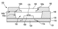
상기 발광 모듈(100)의 제1 실시 예는, 도 1 내지 도 4에 도시된 바와 같이, 관통 홀(110a)이 형성된 세라믹 기판(110)과, 상기 관통 홀(110a) 내에 배치되는 방열 블록(120)과, 상기 세라믹 기판(110) 상에 배치되며 캐비티(cavity, 150)를 형성하는 측벽을 갖는 몸체(140)와, 상기 방열 블록(120) 상에 배치되는 서브마운트(sub mount, 160)와, 상기 서브마운트(160) 상에 배치되는 적어도 하나 이상의 발광 칩(170)과, 상기 몸체(140) 상에 배치되며 관통 홀(180a)이 형성된 캡(cap, 180)과, 상기 캡(180)의 관통 홀(180a) 내에 배치되는 투명 창(190)을 포함한다.1 to 4, the first embodiment of the
상기 세라믹 기판(110)은 단일 층의 세라믹 기판 또는 다층의 세라믹 기판일 수 있다. The
상기 세라믹 기판(110)이 단일 층의 세라믹 기판인 경우, 고온 동시 소성 세라믹(high temperature co-fired ceramic: HTCC) 기술을 이용하여 구현될 수 있다. 이때, 상기 고온동시소성 세라믹(HTCC)은 1200℃ 이상의 고온에서 세라믹 시트들을 동시소성하여 형성될 수 있다.When the
상기 세라믹 기판(110)이 다층의 세라믹 기판인 경우, 예를 들어, 고온 동시 소성 세라믹(high temperature co-fired ceramic: HTCC) 또는 저온 동시 소성 세라믹(Low Temperature Cofired Ceramics: LTCC)으로 구성될 수 있다. When the
상기 세라믹 기판(110)이 다층의 세라믹 기판인 경우, 각 층의 두께는 동일할 수도 있고, 다를 수도 있으며, 이에 대해 제한을 두지 않는다.When the
상기 세라믹 기판(110)은 질화물 또는 산화물의 절연성 재질로 이루어질 수 있다. 예를 들어, SiO2, SixOy, Si3Ny, SiOxNy, Al2O3, 또는 AlN을 포함할 수 있다.The
상기 세라믹 기판(110)은 메탈에 비해 열 전도성이 떨어지기 때문에, 방열 특성을 보상하기 위하여 메탈 슬러그(metal slug)로 이루어진 상기 방열 블록(120)을 동시 소성(Co-fired)하거나, 또는 AgCu로 본딩하여 열처리 후 결합 또는 삽입하여 사용할 수 있다.Since the thermal conductivity of the
상기 세라믹 기판(110)은 상기 발광 칩(170)이 위치하는 공간과 분리된 위치에 제너다이오드가 탑재될 수 있다.A zener diode may be mounted on the
상기 세라믹 기판(110)에는 관통 홀(110a)이 형성되며, 상기 몸체(140) 내부에 캐비티(150)가 형성될 경우 상기 캐비티(150)는 상기 관통 홀(110a) 상에 형성될 수 있다.A through
상기 세라믹 기판(110)의 관통 홀(110a) 내에 상기 방열 블록(120)이 삽입되어 배치된다.The
상기 세라믹 기판(110)의 관통 홀(110a)은 도 4에 도시된 바와 같이, 관통 홀(110a)이 단차 모양으로 형성되어 상기 방열 블록(120)과의 접촉 면적을 넓힘으로써 방열 효과를 증대시킬 수 있다.As shown in FIG. 4, the through-
상기 방열 블록(120)은 상기 발광 칩(170)에서 발생된 열을 방열하는 역할을 한다. 따라서, 상기 방열 블록(120)은 열 전도성이 우수한 금속을 포함할 수 있다. 예를 들어, CuW, CuMo와 같이 Cu가 포함된 합금, Cu 단일 금속, Mo, W, Au 및 Ag 중 적어도 하나를 포함할 수 있다.The
상기 발광 칩(170)에서 발생한 열이 열 전도성이 우수한 상기 방열 블록(120)을 통해 외부로 방출되어 발광 모듈(100)의 방열 특성이 개선되고 신뢰성이 향상될 수 있다. 그리고 상기 방열 블록(120)은 동시 소성(Co-fired)되거나, 또는 AgCu로 본딩하여 열 처리 후 상기 세라믹 기판(110)의 관통 홀(110a)에 결합 또는 삽입하여 사용될 수 있다.Heat generated in the
상기 세라믹 기판(110)과 상기 방열 블록(120)의 열팽창 계수를 고려할 때, 예를 들어 상기 세라믹 기판(110)이 HTCC 기술을 이용하여 구현될 경우 CuW을 포함한 방열 블록(120)을 삽입하여 사용하는 것이 열에 안정적이고, 상기 세라믹 기판(110)이 LTCC 기술을 이용하여 구현될 경우 Ag를 포함한 방열 블록(120)을 결합 또는 삽입하여 사용하는 것이 열에 안정적일 수 있다.Considering the thermal expansion coefficient of the
상기 세라믹 기판(110)과 상기 방열 블록(120)은 구성되는 물질이 달라 열 팽창 계수가 차이가 나기 때문에, 상기 방열 블록(120)을 상기 세라믹 기판(110)에 삽입한 후 동시-소성 가공을 거치거나, 발광 모듈의 사용 중 상기 발광 칩(170)에서 발생하는 열에 의해 상기 방열 블록(120)이 팽창하면서, 상기 발광 칩(170)이 실장되는 상기 방열 블록(120)의 상면이 볼록하게 돌출되어 나올 수 있다.Since the materials of the
상기 방열 블록(120)의 상면이 볼록하게 돌출되면 상기 발광 칩(170)과의 접촉 불량이 발생하여 신뢰성에 문제가 발생할 수 있다.If the upper surface of the
따라서, 상기 발광 칩(170)과 상기 방열 블록(120) 사이에 제1 돌출방지층(130)를 위치시켜, 상기 방열 블록(120)의 상면이 상기 발광 칩(170) 방향으로 돌출되는 것을 방지할 수 있다.The first
상기 제1 돌출방지층(130)은 상기 세라믹 기판(110) 및 상기 방열 블록(120) 상에 배치되거나, 상기 세라믹 기판(110)과 일체로 형성하여 상기 세라믹 기판(110)의 일부를 이룰 수도 있다.The first
또한, 상기 세라믹 기판(110)과 상기 방열 블록(120)의 하부에도 제2 돌출방지층(131)이 배치될 수 있다. 이는, 상기 방열 블록(120)의 상면 뿐만 아니라 상기 방열 블록(120)의 하면에도 볼록하게 돌출되어 나올 수 있기 때문에, 상기 세라믹 기판(110) 및 상기 방열 블록(120)의 하부에도 상기 제2 돌출방지층(131)을 배치할 수 있다.Also, a second
상기 제1 돌출방지층(130) 상에는 캐비티(150)가 내측에 형성된 몸체(140)가 배치되어 있다. 상기 몸체(140)의 측벽(140a)은 경사면으로 이루어질 수 있다. 또는, 상기 몸체(140)의 측벽(140a)은 계단형 또는 수직면으로 이루어질 수도 있다.On the first
상기 몸체(140)의 측벽(140a)은 상기 발광 칩(170)에서 발생된 빛을 반사시켜 오픈 영역인 상기 캐비티(150)로 진행하도록 하여 상기 발광 모듈(100)의 광 추출 효율을 향상시킬 수 있다.The
이러한 경사면 또는 계단 형상 또는 수직면의 상기 측벽(140a)은 드릴링으로 통해 기계적으로 가공하거나, 상기 몸체(140)가 다층의 세라믹 기판으로 구성된 경우 길이가 서로 다른 복수의 세라믹 층을 적층하여 소성함으로써 구현될 수 있으나, 구현 방법에 대해서는 제한을 두지 않는다.The
또한, 상기 몸체(140)의 측벽(140a)과 상기 몸체(140)의 바닥면의 적어도 일부에 반사층이 코팅될 수도 있다.In addition, a reflective layer may be coated on at least a part of the
상기 몸체(140)를 구성하는 세라믹은 공정상 캐비티(150)를 형성하는 것이 용이하고 열에 강한 장점이 있다. The ceramic constituting the
상기 제1 돌출 방지층(130) 상에는 상기 서브마운트(160)가 배치될 수 있다.The sub-mount 160 may be disposed on the first
상기 서브마운트(160)는 도전성 기판 또는 절연성 기판일 수 있으며, 예를 들어, Si, SiC 또는 AlN 등 열 전도율과 열팽창 계수를 고려한 물질들을 포함할 수 있다.The
상기 서브마운트(160) 상에는 도전성 패턴(미도시)이 형성될 수 있으며, 상기 도전성 패턴에 상기 발광 칩(170)이 전기적으로 연결될 수 있다. 예를 들어, Au 페이스트를 이용한 본딩 또는 Au-Sn 유테틱(Eutectic) 본딩으로 고정될 수 있다.A conductive pattern (not shown) may be formed on the
상기 발광 칩(170)에서 발생된 열이 상기 서브마운트(160)를 거쳐 상기 방열 블록(120)을 통해 외부로 방출되므로, 상기 서브마운트(160)는 열 전도성이 우수한 재질로 이루어질 수 있다.Since the heat generated from the
상기 서브마운트(160)가 상기 방열 블록(120) 상에 배치되므로, 상기 발광 칩(170)에서 발생된 열이, 상대적으로 열 전도율이 떨어지는 상기 세라믹 기판(110) 대신에 열 전도성이 우수한 상기 방열 블록(120)을 통해 외부로 방출되므로 상기 발광 모듈(100)의 신뢰성이 향상될 수 있다.Since the
또한, 상기 방열 블록(120)에 상기 발광 칩(170)을 직접 실장할 경우, 상기 발광 칩(170)이 실장되는 상기 방열 블록(120)의 상면이 플랫(flat)하지 않을 경우, 상기 발광 칩(170)이 들뜨거나 불안정하게 본딩되어 방열성이 저하될 수 있는데, 상기 서브마운트(160) 상에 상기 발광 칩(170)을 배치함으로써 이러한 문제점을 최소화할 수 있다.When the upper surface of the
상기 방열 블록(120)은 상기 발광 칩(170)에서 발생된 열을 외부로 방출하여 발광 모듈(100)의 신뢰성을 유지하는 역할을 하므로, 상기 방열 블록(120)과 상기 발광 칩(170)은 서로 수직적으로 중첩되게 배치될 수 있다.The
상기 발광 칩(170)은 복수의 화합물 반도체 층, 예를 들어 3족-5족 원소의 반도체 층을 이용한 LED(Light Emitting Diode)를 포함하며, LED는 청색, 녹색 또는 적색 등과 같은 광을 방출하는 유색 LED이거나 UV LED일 수 있다. LED의 방출 광은 다양한 반도체를 이용하여 구현될 수 있으며, 이에 대해 한정하지는 않는다.The
특히, 상기 세라믹 기판(110) 및 상기 몸체(140)는 무기 재질의 세라믹으로 이루어져 있으므로, 약 200∼405㎚의 파장을 갖는 심 자외선(Deep UV) LED 또는 근 자외선(Near UV) LED를 포함한 발광 칩을 사용하더라도 발광 칩에서 방출된 자외선 광에 의해 상기 상부 및 하부 몸체가 변색되거나 변질될 우려가 없어 발광 모듈의 신뢰성을 유지할 수 있다.Particularly, since the
상기 발광 칩(170)은 플립칩으로 본딩될 수 있다. 또는, 상기 발광 칩(170)은 Au 페이스트를 이용한 본딩 또는 Au-Sn 유테틱(Eutectic) 본딩으로 고정될 수 있다.The
계속해서, 상기 몸체(140) 상에는 투명 창(190)이 관통 홀(180a)에 배치된 캡(180)이 배치될 수 있다. A
상기 캡(180)의 관통 홀(180a)은 단차면이 형성될 수 있다. 이때, 상기 관통 홀(180a)의 단차면은 도 4와 같이, 상기 관통 홀(180a)의 상부 직경이 하부 직경보다 크게 형성될 수 있다. 상기 투명 창(190)은 상기 관통 홀(180a)의 단차면과 대향되도록 외주면에 단차가 형성되어, 상기 캡(180)의 관통 홀(180a) 내부에 배치된다.The through
상기 관통 홀(180a)는 원형(circle)의 홀일 수 있다. 여기서, 관통 홀(180a)의 형상이 원형으로 한정되는 것은 아니다. 예를 들면, 상기 관통 홀(180a)은 사각형(quadrangle)의 홀일 수도 있다. 좀 더 구체적으로, 상기 관통 홀(180a)은 정사각형(square)의 홀일 수도 있고, 직사각형(rectangle)의 홀일 수도 있다. 또한, 상기 관통홀(180a)은 원형과 사각형뿐만 아니라 다각형 형상일 수도 있다. 상기 관통 홀(180a)의 다양한 형상에 대응하여 투명 창(190)은 상기 관통 홀(180a)의 형상에 대응하는 형상을 가질 수 있다.The through
또한, 상기 캡(180)은 하부에 단차면(180b)이 형성될 수 있다. 이에 의해, 상기 캡(180)이 상기 몸체(140) 상면(140b)과 결합시, 상기 단차면(180b)을 갖는 하부 일부가 상기 캐비티(150) 내부로 삽입되게 된다.The
상기 캡(180)과 상기 몸체(140)는, 진공 상태 또는 질소(N2) 가스에서 Au-Sn 유테틱(Eutectic) 본딩으로 밀봉(Sealing)처리하여 결합될 수 있다. The
상기 구성을 갖는 상기 캡(180)은 코바(Kovar)를 포함한 금속 재질 중 하나를 사용하여 형성될 수 있다.The
상기 투명 창(190)은 상기 발광 칩(170)에서 발생된 빛을 흡수하지 않고 외부로 통과시킬 수 있도록 투명한 재질과 비 반사 코팅막으로 이루어질 수 있다. 예를 들어, SiO2(Quartz, UV Fused Silica), Al2O3(Sapphire), LiF, MgF2, CaF2, Low Iron Transparent Glass, B2O3를 포함한 글라스(Glass) 재질 중 어느 하나로 구성될 수 있다.The
상기 투명 창(190)은, 상기 발광 칩(170)이 UV LED인 경우, 상기 발광 칩(170)에서 방출된 자외선 광이 상기 발광 모듈(100) 외부의 유기물을 파괴 또는 변질시키는 것을 방지하는 역할을 할 수 있다.The
상기 투명 창(190)과 상기 캐비티(150) 사이의 공간은 진공 상태일 수도 있고, 질소(N2) 가스 또는 포밍 가스(forming gas)로 충진될 수도 있다.The space between the
또한, 상기 발광 모듈(100)은, 상기 세라믹 기판(110)과 상기 방열 블록(120)의 하부에 방열 패드(미도시)가 배치될 수 있다.The
상기 발광 칩(170)에서 발생된 열이 상기 서브마운트(160)와 상기 방열 블록(120)을 거쳐 상기 방열 패드를 통해 외부로 방출되므로, 상기 방열 패드는 열 전도성이 우수한 물질일 수 있다. 예를 들어, Ag, Au 또는 Cu 중 어느 하나를 포함한 금속일 수 있다.Since the heat generated from the
또한, 상기 방열 패드와 상기 세라믹 기판(110) 사이, 그리고 상기 방열 패드와 상기 방열 블록(120) 사이에는 열전 시트(thermal sheet)(미도시)가 배치될 수도 있다. 상기 열전 시트는 우수한 열 전도성과 전기 절연성 및 난연성을 가져서 발열 부위와 방열 패드를 밀착시켜 줌으로써 열 전달 효과를 극대화시킬 수 있다.A thermal sheet (not shown) may be disposed between the heat dissipation pad and the
또한, 상기 발광 모듈(100)은, 상기 발광 칩(170)을 포위하도록 상기 캐비티(150) 내에 형성되는 몰딩부(미도시)를 더 포함할 수 있다. 이때, 상기 몰딩부는, 형광체가 혼합된 고 굴절률 또는 저 굴절률 Si계 Resin 또는 하이브리드계 Resin 중 적어도 하나를 포함할 수 있다.
The
제1 실시 예의 In the first embodiment 설계치수Design dimensions 예 Yes
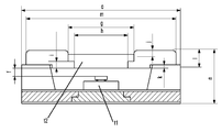
도 5 내지 도 7은 발광 모듈의 설계치수 예를 도시한 단면도이다.5 to 7 are sectional views showing an example of the design dimensions of the light emitting module.
먼저, 도 5를 참조하면, 상기 세라믹 기판(110)과 상기 제1 및 제2 돌출 방지층(130,131)의 높이(a)는 0.2mm 이상 0.6mm 이하일 수 있고, 바람직하게는 0.4㎜일 수 있다. 상기 몸체(140)의 높이(b)는 0.4mm 이상 1.0mm 이하일 수 있고, 바람직하게는 0.7㎜일 수 있다., 상기 제1 및 제2 돌출 방지층(130,131)을 포함한 상기 세라믹 기판(110)과 상기 몸체(140)의 총 높이(c)는 0.6mm 이상 1.6mm이하일 수 있고, 바람직하게는 1.1㎜로 설계될 수 있다. Referring to FIG. 5, the height a of the
그리고, 상기 서브마운트(160)와 상기 발광 칩(170)의 높이(d)는 0.2mm 이상 0.6mm 이하일 수 있고, 바람직하게는 0.4㎜일 수 있다. 또한, 상기 발광 칩(170)과 상기 몸체(140)의 최상부까지의 높이(e)는 0.1mm 이상 0.5mm 이하일 수 있고, 바람직하게는 0.3㎜로 설계될 수 있다.The height (d) of the
도 6을 참조하면, 상기 서브마운트(160)의 두께(t1)는 0.05mm 이상 0.45mm이하일 수 있고, 바람직하게는 0.25㎜일 수 있다. 상기 발광 칩(170)과 상기 투명 창(190) 사이의 간격(f)은 0.1mm 이상 0.3mm 이하일 수 있고, 바람직하게는 0.2㎜일 수 있다. 상기 투명 창(190)의 상부 직경(g)은 1.7mm 이상 2.1mm 이하일 수 있고, 바람직하게는 1.9㎜일 수 있다. 상기 투명 창(190)의 하부 직경(h)은 1.3mm 이상 1.7mm 이하일 수 있고, 바람직하게는 1.5㎜일 수 있다. 상기 투명 창(190)의 두께(t2)는 0.3mm 이상 0.5mm 이하일 수 있고, 바람직하게는 0.4㎜일 수 있다. 상기 캡(180)의 하면에서 단차면까지의 높이(i)는 0.1mm 이상 0.3mm 이하일 수 있고, 바람직하게는 0.2㎜일 수 있다. 상기 투명 창(190) 상부와 상기 캡(180) 상부 사이의 간격(j)은 0.1mm 이상 0.3mm 이하일 수 있고, 바람직하게는 0.2㎜일 수 있다. 상기 캡(180) 하부에 형성된 단차면(180b)의 높이(k)는 0.05mm 이상 0.2mm 이하일 수 있고, 바람직하게는 0.1㎜일 수 있다. 상기 캡(180)의 측면 높이(l)는 0.2mm 이상 0.6mm 이하일 수 있고, 바람직하게는 0.4㎜일 수 있다. 상기 캡(180)의 직경(m)은 4.0mm 이상 4.4mm 이하일 수 있고, 바람직하게는 4.2㎜일 수 있다. 상기 제2 돌출 방지층(131)에서 상기 캡(180) 상부까지의 높이(n)는 1.3mm 이상 1.7mm 이하일 수 있고, 바람직하게는 1.5㎜일 수 있다. 상기 세라믹 기판(110) 및 상기 몸체(140)의 직경(o)은 4.3mm 이상 4.7mm 이하일 수 있고, 바람직하게는 4.5㎜로 설계될 수 있다.Referring to FIG. 6, the thickness t1 of the
도 7을 참조하면, 상기 캡(180) 하부에 형성된 상기 단차면(180b)에는 AuSn층(181)이 5∼7㎛ 두께와 너비(p) 0.4mm 이상 0.7mm 이하, 바람직하게는 0.45㎜로 형성되어 있고, 상기 캡(180)의 단차면(180b)과 결합되는 상기 몸체(140)의 상면(140b)에는 Au 패턴(141)이 5㎛ 이상의 두께와 너비(q) 0.5mm 이상 0.8mm 이하, 바람직하게는 0.5㎜로 형성될 수 있다. 여기서, AuSn층(181)의 너비(p)는 Au 패턴(141)의 너비(q)보다 작을 수 있다.7, an
상기 캡(180) 하부에 형성된 상기 단차면(180b)의 너비(r)는 0.5mm 이상 0.9mm 이하일 수 있고, 바람직하게는 0.7㎜일 수 있다. 상기 캡(180)의 관통 홀에 형성된 단차면(180a)의 너비(s)는 0.1mm 이상 0.3mm 이하일 수 있고, 바람직하게는 0.2㎜일 수 있다. 상기 투명 창(190) 상부와 상기 캡(180) 상부 사이의 간격(z)은 0 초과 0.2mm 이하일 수 있고, 바람직하게는 0.1㎜일 수 있다. 상기 캡(180)의 두께(x)는 0.3mm 이상 0.7mm 이하일 수 있고, 바람직하게는 0.5㎜일 수 있다. 상기 몸체(140)의 너비(u)는 0.6mm 이상 1.0mm 이하일 수 있고, 바람직하게는 0.8㎜일 수 있다. 상기 캡(180)과 상기 몸체(140)의 결합시 상기 캡(180)과 상기 몸체(140) 사이의 간격(v)은 0.03mm 이상 0.07mm 이하일 수 있고, 바람직하게는 0.05㎜일 수 있다. 상기 캡(180)의 상부에서 단차면(180b)까지의 높이(y1)는 0.3mm 이상 0.5mm 이하일 수 있고, 바람직하게는 0.4mm일 수 있다. 상기 캡(180)의 하부에서 단차면(180a)까지의 높이(y2)는 0.1mm 이상 0.3mm 이하일 수 있고, 바람직하게는 0.2mm일 수 있다. 상기 몸체(140)의 상면(140b)에 형성된 Au 패턴(141)과 상기 몸체(140) 가장자리 사이의 간격(w)은 0.1mm 이상 0.2mm 이하일 수 있고, 바람직하게는 0.15㎜로 설계될 수 있다.
The width r of the stepped
제2 실시 예의 구성 예Configuration Example of Second Embodiment
도 8 내지 도 10은 제2 실시 예에 의한 발광 모듈의 도면으로, 도 8은 단면 구성도이고, 도 9 및 도 10은 발광 모듈의 설계치수 예를 도시한 단면도이다.Figs. 8 to 10 are views of a light emitting module according to a second embodiment, Fig. 8 is a sectional view, and Fig. 9 and Fig. 10 are sectional views showing an example of the design dimensions of the light emitting module.
상기 발광 모듈(200)의 제2 실시 예는, 도 8에 도시된 바와 같이, 관통 홀(110a)이 형성된 세라믹 기판(110)과, 상기 관통 홀(110a) 내에 배치되는 방열 블록(120)과, 상기 세라믹 기판(110) 상에 배치되며 측벽 내부에 캐비티(150)를 갖는 몸체(140)와, 상기 방열 블록(120) 상에 배치되는 서브마운트(160)와, 상기 서브마운트(160) 상에 배치되는 적어도 하나 이상의 발광 칩(170)과, 상기 몸체(140) 상에 배치되며 관통 홀(280a)이 형성된 캡(280)과, 상기 캡(280)의 관통 홀(280a) 내에 배치되는 투명 창(290)을 포함한다.8, the second embodiment of the
상기 발광 모듈(200)은 상기 방열 블록(120)의 상면이 상기 발광 칩(170) 방향으로 돌출되는 것을 방지하기 위해, 상기 발광 칩(170)과 상기 방열 블록(120) 사이와 상기 세라믹 기판(110) 상에 제1 돌출방지층(130)이 배치되어 있다. 또한, 상기 세라믹 기판(110)과 상기 방열 블록(120)의 하부에도 제2 돌출방지층(131)이 배치되어 있다.The
상기 발광 모듈(200)의 제2 실시 예는 상기 제1 실시 예(도 4)와 비교할 때, 상기 캡(280)과 상기 투명 창(290)의 구성만 다르고 나머지 구성은 동일하다.The second embodiment of the
상기 캡(280)은 중앙에 관통 홀(280a)이 형성되어 있고, 상기 관통 홀(280a)에 상기 투명 창(290)이 배치되어 있다. A through
상기 관통 홀(280a)은 원형(circle)의 홀일 수 있다. 여기서, 관통 홀(280a)의 형상이 원형으로 한정되는 것은 아니다. 예를 들면, 상기 관통 홀(280a)은 사각형(quadrangle)의 홀일 수도 있다. 좀 더 구체적으로, 상기 관통 홀(280a)은 정사각형(square)의 홀일 수도 있고, 직사각형(rectangle)의 홀일 수도 있다. 또한, 상기 관통홀(280a)은 원형과 사각형뿐만 아니라 다각형 형상일 수도 있다. 상기 관통 홀(280a)의 다양한 형상에 대응하여 투명 창(290)은 상기 관통 홀(280a)의 형상에 대응하는 형상을 가질 수 있다.The through
상기 캡(280)은 단차면을 가질 수 있다. 이때, 상기 캡(280)의 단차면에 의해, 도 8과 같이, 상기 관통 홀(280a)의 상부 직경이 하부 직경보다 작게 형성될 수 있다. 즉, 상기 단차면은 상기 캡(280)의 하부에 형성되어 있다.The
상기 투명 창(290)은 상기 캡(280)의 단차면 상에 배치된다. 이에 따라, 상기 투명 창(290)은 평판 형태로 구성될 수 있다.The
상기 캡(280)과 상기 몸체(140)는, 진공 상태 또는 질소(N2) 가스에서 Au-Sn 유테틱(Eutectic) 본딩으로 밀봉(Sealing)처리하여 결합될 수 있다. The
상기 구성을 갖는 상기 캡(280)은 코바(Kovar)를 포함한 금속 재질 중 하나를 사용하여 형성될 수 있다.The
상기 투명 창(290)은 상기 발광 칩(170)에서 발생된 빛을 흡수하지 않고 외부로 통과시킬 수 있도록 투명한 재질과 비 반사 코팅막으로 이루어질 수 있다. 예를 들어, SiO2(Quartz, UV Fused Silica), Al2O3(Sapphire), LiF, MgF2, CaF2, Low Iron Transparent Glass, B2O3를 포함한 글라스(Glass) 재질 중 어느 하나로 구성될 수 있다.The
상기 투명 창(290)은, 상기 발광 칩(170)이 UV LED인 경우, 상기 발광 칩(170)에서 방출된 자외선 광이 상기 발광 모듈(100) 외부의 유기물을 파괴 또는 변질시키는 것을 방지하는 역할을 할 수 있다.The
상기 투명 창(290)과 상기 캐비티(150) 사이의 공간은 진공 상태일 수도 있고, 질소(N2) 가스 또는 포밍 가스(forming gas)로 충진될 수도 있다.The space between the
또한, 상기 발광 모듈(200)은, 상기 세라믹 기판(110)과 상기 방열 블록(120)의 하부에 방열 패드(미도시)가 배치될 수 있다.A heat dissipation pad (not shown) may be disposed below the
상기 발광 칩(170)에서 발생된 열이 상기 서브마운트(160)와 상기 방열 블록(120)을 거쳐 상기 방열 패드를 통해 외부로 방출되므로, 상기 방열 패드는 열 전도성이 우수한 물질일 수 있다. 예를 들어, Ag, Au 또는 Cu 중 어느 하나를 포함한 금속일 수 있다.Since the heat generated from the
또한, 상기 방열 패드와 상기 세라믹 기판(110) 사이, 그리고 상기 방열 패드와 상기 방열 블록(120) 사이에는 열전 시트(thermal sheet)(미도시)가 배치될 수도 있다. 상기 열전 시트는 우수한 열 전도성과 전기 절연성 및 난연성을 가져서 발열 부위와 방열 패드를 밀착시켜 줌으로써 열 전달 효과를 극대화시킬 수 있다.A thermal sheet (not shown) may be disposed between the heat dissipation pad and the
또한, 상기 발광 모듈(200)은, 상기 발광 칩(170)을 포위하도록 상기 캐비티(150) 내에 형성되는 몰딩부(미도시)를 더 포함할 수 있다. 이때, 상기 몰딩부는, 형광체가 혼합된 고 굴절률 또는 저 굴절률 Si계 Resin 또는 하이브리드계 Resin 중 적어도 하나를 포함할 수 있다.
The
제2 실시 예의 In the second embodiment 설계치수Design dimensions 예 Yes
상기 제2 실시 예에 의한 발광 모듈(200)에서, 세라믹 기판(110), 제1 및 제2 돌출 방지층(130,131), 몸체(140), 서브마운트(160) 및 발광 칩(170)에 관련된 수치는 도 5에 도시된 수치와 같다.
In the
도 9를 참조하면, 상기 발광 칩(170)과 상기 투명 창(290) 사이의 간격(f')은 0.2mm 이상 0.4mm 이하일 수 있고, 바람직하게는 0.3㎜일 수 있다. 상기 투명 창(290)의 최대 직경(g')은 1.7mm 이상 2.1mm 이하일 수 있고, 바람직하게는 1.9㎜일 수 있다. 상기 투명 창(290)의 두께(t2')는 0.2mm 이상 0.4mm 이하일 수 있고, 바람직하게는 0.3㎜일 수 있다. 상기 캡(280)의 하면에서 단차면까지의 높이(i')는 0.2mm 이상 0.4mm 이하일 수 있고, 바람직하게는 0.3㎜일 수 있다. 상기 투명 창(290) 상부와 상기 캡(280) 상부 사이의 간격(j')은 0.1mm 이상 0.3mm 이하일 수 있고, 바람직하게는 0.2㎜일 수 있다. 상기 캡(280)의 측면 높이(l')는 0.3mm 이상 0.7mm 이하일 수 있고, 바람직하게는 0.5㎜일 수 있다. 상기 캡(280)의 직경(m')은 4.0mm 이상 4.4mm 이하일 수 있고, 바람직하게는 4.2㎜일 수 있다. 상기 제2 돌출 방지층(131)에서 상기 캡(280) 상부까지의 높이(n')는 1.4mm 이상 1.8mm 이하일 수 있고, 바람직하게는 1.6㎜일 수 있다. 상기 투명 창(290)의 상부 직경(h')은 1.3mm 이상 1.7mm 이하일 수 있고, 바람직하게는 1.5㎜일 수 있다. 상기 세라믹 기판(110) 및 상기 몸체(140)의 직경(o')은 4.3mm 이상 4.7mm 이하일 수 있고, 바람직하게는 4.5㎜로 설계될 수 있다.Referring to FIG. 9, the distance f 'between the light emitting
도 10을 참조하면, 상기 몸체(140)의 상면(140b)과 결합하는 상기 캡(280) 하부에 AuSn층(281)이 5∼7㎛ 두께와 너비(p') 0.4mm 이상 0.7mm 이하, 바람직하게는 0.45㎜로 형성되어 있고, 상기 캡(280)의 하부와 결합되는 상기 몸체(140)의 상면(140b)에 Au 패턴(141)이 5㎛ 이상의 두께와 너비(q') 0.5mm 이상 0.8mm 이하, 바람직하게는 0.5㎜로 형성되어 있다. 여기서, AuSn층(281)의 너비(p)는 Au 패턴(141)의 너비보다 작을 수 있다.10, an
상기 캡(280)의 관통 홀(280a)에 형성된 단차면의 너비(s')는 0.1mm 이상 0.3mm 이하일 수 있고, 바람직하게는 0.2㎜일 수 있다. 상기 투명 창(290) 상부와 상기 캡(280) 상부 사이의 간격(z')은 0.1mm 이상 0.3mm 이하일 수 있고, 바람직하게는 0.2㎜일 수 있다. 상기 캡(280)의 두께(x')는 0.3mm 이상 0.7mm 이하일 수 있고, 바람직하게는 0.5㎜일 수 있다. 상기 몸체(140)의 너비(u')는 0.6mm 이상 1.0mm 이하일 수 있고, 바람직하게는 0.8㎜일 수 있다. 상기 몸체(140)의 상면(140b)에 형성된 Au 패턴과 상기 몸체(140) 가장자리 사이의 간격(w')은 0.1mm 이상 0.2mm 이하일 수 있고, 바람직하게는 0.15㎜로 설계될 수 있다.
The width s' of the stepped surface formed in the through
이와 같이 구성된 실시 예에 따른 발광 모듈은, 관통 홀을 가지는 세라믹 기판, 상기 관통 홀 내에 배치되는 방열 블록, 상기 세라믹 기판 상에 배치되며 측벽 내부에 캐비티를 갖는 몸체, 상기 방열 블록 상에 배치되는 서브마운트, 상기 서브마운트 상에 배치되는 발광 칩, 상기 몸체 상에 배치되며 관통 홀이 형성된 캡 및, 상기 캡의 관통 홀 내에 배치되는 투명 창을 포함하여 구성함으로써, 상기 투명 창과 상기 발광 칩 사이의 간격을 줄일 수 있어 광손실을 최소화할 수 있고 이로 인해 광출력을 향상시킬 수 있다. 또한, 유테틱 본딩(Eutectic Bonding)을 사용하여 공정 차별화를 구현할 수 있고, 고 방열 및 장 수명을 구현할 수 있다. 그리고, 범용 설계가 가능하며, 콤팩트(compact) 설계를 통해 소형화가 가능하다. 또한, 개면 박리에 의한 변색, 변질을 방지할 수 있고, 외부의 수분이나 공기가 내부로 침투하지 못하도록 구조를 개선할 수 있으며, 제조 공정 및 비용을 줄일 수 있어, 본 발명의 기술적 과제를 해결할 수가 있다.
The light emitting module according to this embodiment includes a ceramic substrate having a through hole, a heat dissipation block disposed in the through hole, a body disposed on the ceramic substrate and having a cavity inside the side wall, A light emitting chip disposed on the submount, a cap disposed on the body and having a through-hole, and a transparent window disposed in the through-hole of the cap, wherein a gap between the transparent window and the light emitting chip The light loss can be minimized and the light output can be improved. In addition, it is possible to realize process differentiation by using eutectic bonding and realize high heat dissipation and long service life. And it can be general-purpose design, and it can be downsized by compact design. In addition, it is possible to prevent discoloration and deterioration due to separation on the front surface, improve the structure so that external moisture or air can not penetrate into the interior, reduce the manufacturing process and cost, and solve the technical problem of the present invention have.
이상에서 실시 예를 중심으로 설명하였으나 이는 단지 예시일 뿐 본 발명을 한정하는 것이 아니며, 본 발명이 속하는 분야의 통상의 지식을 가진 자라면 본 실시 예의 본질적인 특성을 벗어나지 않는 범위에서 이상에 예시되지 않은 여러 가지의 변형과 응용이 가능함을 알 수 있을 것이다. 예를 들어, 실시 예에 구체적으로 나타난 각 구성 요소는 변형하여 실시할 수 있는 것이다. 그리고 이러한 변형과 응용에 관계된 차이점들은 첨부된 청구 범위에서 규정하는 본 발명의 범위에 포함되는 것으로 해석되어야 할 것이다.
While the present invention has been particularly shown and described with reference to exemplary embodiments thereof, it is to be understood that the invention is not limited to the disclosed exemplary embodiments, but, on the contrary, It will be understood that various modifications and applications are possible. For example, each component specifically shown in the embodiments can be modified and implemented. It is to be understood that all changes and modifications that come within the meaning and range of equivalency of the claims are therefore intended to be embraced therein.
100 : 발광 모듈의 제1 실시 예
110 : 세라믹 기판
120 : 방열 블록
130 : 제1 돌출 방지층
131 : 제2 돌출 방지층
140 : 몸체
150 : 캐비티
160 : 서브마운트
170 : 발광 칩
180 : 캡(Cap)
190 : 투명 창
200 : 발광 모듈의 제2 실시 예
280 : 캡(Cap)
290 : 투명 창100: First embodiment of light emitting module
110: ceramic substrate
120: Heat block
130: first protrusion preventing layer
131: second protrusion preventing layer
140: Body
150: cavity
160: Submount
170: Light emitting chip
180: Cap (Cap)
190: Transparent window
200: Second Embodiment of Light Emitting Module
280: Cap (Cap)
290: Transparent window
Claims (21)
상기 관통 홀에 배치되는 방열 블록;
상기 세라믹 기판 상에 배치되며 캐비티를 형성하는 측벽을 갖는 몸체;
상기 캐비티 내부의 상기 방열 블록 상에 배치되는 발광 칩;
상기 몸체 상에 배치되며 관통 홀을 갖는 캡;
상기 캡의 관통 홀에 배치되는 투명 창;
상기 세라믹 기판의 상면과 상기 방열 블록의 상면을 직접적으로 접촉하며, 상기 방열 블록의 상면 전체를 덮도록 배치된 제1 돌출방지층; 및
상기 세라믹 기판의 하면과 상기 방열 블록의 하면을 직접적으로 접촉하며, 상기 방열 블록의 하면 전체를 덮도록 배치된 제2 돌출방지층;을 포함하고,
상기 세라믹 기판의 상면에서의 상기 세라믹 기판의 관통 홀의 최대 폭은, 상기 세라믹 기판의 하면에서의 상기 세라믹 기판의 관통 홀의 최대 폭보다 작고,
상기 방열 블록은 상기 제2 돌출방지층에 접하는 면이 상기 제1 돌출방지층에 접하는 면보다 더 넓어 지도록 단차를 이루고,
상기 투명 창의 하면과 상기 발광 칩의 상면 사이의 간격은 0.1 mm 이상 0.3 mm 이하이고,
상기 발광 칩의 폭은 상기 방열 블록의 폭보다 작고,
상기 제1 돌출방지층과 상기 제2 돌출방지층과 상기 세라믹 기판의 폭은 동일하고,
상기 제1 돌출방지층과 상기 제2 돌출방지층과 상기 방열 블록의 두께의 합은 0.2mm 이상 0.6mm 이하이고,
상기 캡은 상기 관통 홀을 정의하는 단차면을 포함하고,
상기 단차면에 상기 투명 창이 배치되고,
상기 관통 홀은 상부 직경이 하부 직경보다 더 작고,
상기 투명 창은 상기 단차면과 대응되는 단차면을 포함하며
상기 투명 창의 상면은 상기 캡의 상면보다 낮은, 발광 모듈.
A ceramic substrate including an upper surface and a lower surface, the ceramic substrate having a through hole penetrating the upper surface and the lower surface;
A heat dissipation block disposed in the through hole;
A body disposed on the ceramic substrate and having a side wall defining a cavity;
A light emitting chip disposed on the heat dissipation block inside the cavity;
A cap disposed on the body and having a through hole;
A transparent window disposed in the through hole of the cap;
A first protrusion preventing layer directly contacting the upper surface of the ceramic substrate and the upper surface of the heat dissipation block and covering the entire upper surface of the heat dissipation block; And
And a second protrusion preventing layer directly contacting the lower surface of the ceramic substrate and the lower surface of the heat dissipation block and covering the entire lower surface of the heat dissipation block,
The maximum width of the through hole of the ceramic substrate on the upper surface of the ceramic substrate is smaller than the maximum width of the through hole of the ceramic substrate on the lower surface of the ceramic substrate,
Wherein the heat blocking block has a stepped surface such that a surface thereof contacting the second protrusion preventing layer is wider than a surface contacting the first protrusion preventing layer,
The distance between the lower surface of the transparent window and the upper surface of the light emitting chip is 0.1 mm or more and 0.3 mm or less,
Wherein a width of the light emitting chip is smaller than a width of the heat dissipation block,
The first protrusion preventing layer, the second protrusion preventing layer, and the ceramic substrate have the same width,
The sum of the thickness of the first protrusion preventing layer, the second protrusion preventing layer, and the heat dissipation block is 0.2 mm or more and 0.6 mm or less,
Wherein the cap includes a stepped surface defining the through hole,
The transparent window is disposed on the stepped surface,
Wherein the through hole has an upper diameter smaller than a lower diameter,
Wherein the transparent window includes a stepped surface corresponding to the stepped surface,
Wherein an upper surface of the transparent window is lower than an upper surface of the cap.
상기 발광 모듈은,
상기 발광 칩과 상기 방열 블록 사이에 배치된 서브마운트를 더 포함하고,
상기 서브마운트의 하면의 최대 폭은, 상기 세라믹 기판의 상면에서의 상기 세라믹 기판의 관통 홀의 최대 폭보다 작고,
상기 발광 칩의 최대 폭은 상기 서브마운트의 상면의 최대 폭보다 작은, 발광 모듈.
The method according to claim 1,
The light emitting module includes:
Further comprising a submount disposed between the light emitting chip and the heat dissipation block,
The maximum width of the lower surface of the submount is smaller than the maximum width of the through hole of the ceramic substrate on the upper surface of the ceramic substrate,
Wherein a maximum width of the light emitting chip is smaller than a maximum width of an upper surface of the submount.
상기 캡은 코바를 포함한 금속 재질이고,
상기 캡과 상기 몸체는, Au-Sn 유테틱(Eutectic) 본딩에 의해서 결합된, 발광 모듈.
The method according to claim 1,
Wherein the cap is made of a metal material including cobalt,
Wherein the cap and the body are coupled by Au-Sn eutectic bonding.
상기 발광 칩은 Au 페이스트를 이용한 본딩 또는 Au-Sn 유테틱(Eutectic) 본딩에 의해 고정된, 발광 모듈.
3. The method according to claim 1 or 2,
Wherein the light emitting chip is fixed by bonding using Au paste or Au-Sn eutectic bonding.
상기 세라믹 기판 및 상기 몸체는, 고온 동시 소성 세라믹(high temperature co-fired ceramic: HTCC) 또는 저온 동시 소성 세라믹(Low Temperature Cofired Ceramics: LTCC)으로 이루어지고,
상기 세라믹 기판 및 상기 몸체는, SiO2, SixOy, Si3Ny, SiOxNy, Al2O3, AlN 중 어느 하나를 포함하는, 발광 모듈.
The method according to claim 1,
The ceramic substrate and the body are made of a high temperature co-fired ceramic (HTCC) or a low temperature cofired ceramic (LTCC)
Wherein the ceramic substrate and the body comprise any one of SiO 2 , Si x O y , Si 3 N y , SiO x N y , Al 2 O 3 , and AlN.
상기 방열 블록은 Cu, W, Ag, Mo, CuMo, CuW 중 어느 하나를 포함하고,
상기 투명 창은 SiO2(Quartz, UV Fused Silica), Al2O3(Sapphire), LiF, MgF2, CaF2, Low Iron Transparent Glass, B2O3를 포함한 글라스 재질 중 어느 하나로 이루어지고,
상기 캐비티는 진공 상태이거나, 질소(N2) 가스 또는 포밍 가스(forming gas)가 충진된, 발광 모듈.
The method according to claim 1,
Wherein the heat dissipation block includes any one of Cu, W, Ag, Mo, CuMo and CuW,
Wherein the transparent window is made of any one of glass materials including SiO 2 (Quartz, UV Fused Silica), Al 2 O 3 (Sapphire), LiF, MgF 2 , CaF 2 , Low Iron Transparent Glass, and B 2 O 3 ,
Wherein the cavity is in a vacuum state or filled with nitrogen (N 2 ) gas or forming gas.
상기 발광 칩을 포위하도록 상기 캐비티 내에 형성되는 몰딩부를 더 포함하고,
상기 몰딩부는, 형광체가 혼합된 Si계 레진(Resin) 또는 하이브리드계 레진(Resin) 중 적어도 하나를 포함하는, 발광 모듈.
The method according to claim 1,
And a molding part formed in the cavity to surround the light emitting chip,
Wherein the molding part includes at least one of a Si-based resin or a hybrid-based resin mixed with a phosphor.
상기 세라믹 기판은 회로 패턴을 포함하고, 상기 회로 패턴과 상기 발광 칩이 전기적으로 연결되고,
상기 발광 칩은, 200nm 이상 405㎚이하의 파장을 갖는 심 자외선(Deep UV) LED 칩 또는 근 자외선(Near UV) LED 칩을 포함하고,
상기 세라믹 기판은 상기 발광 칩이 위치하는 공간과 분리된 위치에 제너다이오드가 탑재된, 발광 모듈.
The method according to claim 1,
Wherein the ceramic substrate includes a circuit pattern, the circuit pattern and the light emitting chip are electrically connected,
Wherein the light emitting chip includes a deep UV LED chip or a near UV LED chip having a wavelength of 200 nm or more and 405 nm or less,
And a zener diode is mounted on the ceramic substrate at a position separated from a space where the light emitting chip is located.
상기 캡의 하면은, 상기 몸체의 상면에 배치되는 제1 면, 상기 몸체의 상기 캐비티 내부에 배치되는 제2 면, 및 상기 제1 면과 상기 제2 면 사이에 배치된 단차면을 포함하고,
상기 제2 면과 상기 투명 창의 하면은 동일 평면 상에 배치된, 발광 모듈.
The method according to claim 1,
The lower surface of the cap includes a first surface disposed on an upper surface of the body, a second surface disposed inside the cavity of the body, and a stepped surface disposed between the first surface and the second surface,
And the lower surface of the transparent window and the second surface are disposed on the same plane.
상기 발광 모듈은,
상기 발광 칩과 상기 방열 블록 사이에 배치된 서브마운트를 더 포함하고,
상기 발광 칩의 상면과 상기 투명 창의 하면 사이의 최단 간격은, 상기 발광 칩의 상면과 상기 서브마운트의 하면 사이의 최단 간격보다 작은, 발광 모듈.
The method according to claim 1,
The light emitting module includes:
Further comprising a submount disposed between the light emitting chip and the heat dissipation block,
Wherein the shortest distance between the upper surface of the light emitting chip and the lower surface of the transparent window is smaller than the shortest distance between the upper surface of the light emitting chip and the lower surface of the submount.
Priority Applications (8)
| Application Number | Priority Date | Filing Date | Title |
|---|---|---|---|
| KR1020120087167A KR101973395B1 (en) | 2012-08-09 | 2012-08-09 | Light emitting module |
| JP2013098976A JP6401435B2 (en) | 2012-08-09 | 2013-05-09 | Luminous package |
| US13/924,167 US9893259B2 (en) | 2012-08-09 | 2013-06-21 | Light emitting package |
| EP22165623.4A EP4040518A1 (en) | 2012-08-09 | 2013-07-25 | Light emitting device |
| EP13177955.5A EP2696379B1 (en) | 2012-08-09 | 2013-07-25 | Light emitting device |
| CN201310346581.XA CN103574354B (en) | 2012-08-09 | 2013-08-09 | Light emitting device |
| CN201710194634.9A CN107023760A (en) | 2012-08-09 | 2013-08-09 | Luminescent device |
| US15/863,146 US10388841B2 (en) | 2012-08-09 | 2018-01-05 | Light emitting package |
Applications Claiming Priority (1)
| Application Number | Priority Date | Filing Date | Title |
|---|---|---|---|
| KR1020120087167A KR101973395B1 (en) | 2012-08-09 | 2012-08-09 | Light emitting module |
Publications (2)
| Publication Number | Publication Date |
|---|---|
| KR20140020529A KR20140020529A (en) | 2014-02-19 |
| KR101973395B1 true KR101973395B1 (en) | 2019-04-29 |
Family
ID=48874869
Family Applications (1)
| Application Number | Title | Priority Date | Filing Date |
|---|---|---|---|
| KR1020120087167A Expired - Fee Related KR101973395B1 (en) | 2012-08-09 | 2012-08-09 | Light emitting module |
Country Status (5)
| Country | Link |
|---|---|
| US (2) | US9893259B2 (en) |
| EP (2) | EP2696379B1 (en) |
| JP (1) | JP6401435B2 (en) |
| KR (1) | KR101973395B1 (en) |
| CN (2) | CN107023760A (en) |
Families Citing this family (24)
| Publication number | Priority date | Publication date | Assignee | Title |
|---|---|---|---|---|
| KR101973395B1 (en) * | 2012-08-09 | 2019-04-29 | 엘지이노텍 주식회사 | Light emitting module |
| EP2919284B1 (en) * | 2014-03-14 | 2019-07-03 | Citizen Electronics Co., Ltd. | Light emitting apparatus |
| KR102252156B1 (en) * | 2014-07-08 | 2021-05-17 | 엘지이노텍 주식회사 | Light emitting device package |
| US9481572B2 (en) * | 2014-07-17 | 2016-11-01 | Texas Instruments Incorporated | Optical electronic device and method of fabrication |
| DE112015006331T5 (en) * | 2015-03-19 | 2017-12-14 | Osram Opto Semiconductors Gmbh | Window for covering an optoelectronic semiconductor chip, window comprising a plurality of windows, method for producing windows and optoelectronic semiconductor component |
| WO2016181516A1 (en) * | 2015-05-13 | 2016-11-17 | 三菱電機株式会社 | Semiconductor module |
| CN108027110B (en) * | 2015-09-01 | 2020-07-10 | Lg 伊诺特有限公司 | lighting device |
| JP2017073489A (en) * | 2015-10-08 | 2017-04-13 | エヌイーシー ショット コンポーネンツ株式会社 | Metal-glass lid and DUV-LED device using the same |
| JP6889533B2 (en) * | 2015-10-21 | 2021-06-18 | スタンレー電気株式会社 | Ultraviolet light emitting device and ultraviolet irradiation device |
| JP6712855B2 (en) * | 2015-12-02 | 2020-06-24 | スタンレー電気株式会社 | Ultraviolet light emitting device and ultraviolet irradiation device |
| US10557596B2 (en) * | 2016-02-12 | 2020-02-11 | Lg Innotek Co., Ltd. | Light emitting device package having a black epoxy molding compound (EMC) body and lighting apparatus including the same |
| US10207116B2 (en) | 2016-12-01 | 2019-02-19 | Medtronic, Inc. | Pacing mode switching in a ventricular pacemaker |
| US10864377B2 (en) | 2016-12-01 | 2020-12-15 | Medtronic, Inc. | Pacing mode switching in a ventricular pacemaker |
| JP2019096778A (en) * | 2017-11-24 | 2019-06-20 | 京セラ株式会社 | Lid and optical device |
| JP6687008B2 (en) * | 2017-11-30 | 2020-04-22 | 日亜化学工業株式会社 | Light emitting device |
| FR3075465B1 (en) * | 2017-12-15 | 2020-03-27 | Stmicroelectronics (Grenoble 2) Sas | ELECTRONIC CIRCUIT BOX COVER |
| FR3075466B1 (en) | 2017-12-15 | 2020-05-29 | Stmicroelectronics (Grenoble 2) Sas | ELECTRONIC CIRCUIT BOX COVER |
| JP7109930B2 (en) * | 2018-02-05 | 2022-08-01 | 日機装株式会社 | Fluid sterilizer |
| US10438975B1 (en) * | 2018-03-13 | 2019-10-08 | Innolux Corporation | Display device and method for preparing the same |
| JP7356983B2 (en) * | 2018-08-22 | 2023-10-05 | エーディーワイ株式会社 | UV element package |
| JP7405031B2 (en) * | 2020-07-16 | 2023-12-26 | 日本電気硝子株式会社 | Electronic device and method for manufacturing electronic device |
| CN113707616A (en) * | 2021-07-19 | 2021-11-26 | 中国电子科技集团公司第十三研究所 | Cover plate and ceramic packaging structure |
| WO2023042792A1 (en) * | 2021-09-16 | 2023-03-23 | 旭化成株式会社 | Ultraviolet irradiation device |
| JP2025041057A (en) * | 2023-09-13 | 2025-03-26 | ウシオ電機株式会社 | Light source module and method for manufacturing the light source module |
Citations (1)
| Publication number | Priority date | Publication date | Assignee | Title |
|---|---|---|---|---|
| JP2008109079A (en) * | 2006-09-26 | 2008-05-08 | Kyocera Corp | SURFACE MOUNT LIGHT EMITTING DEVICE WIRING BOARD AND LIGHT EMITTING DEVICE |
Family Cites Families (36)
| Publication number | Priority date | Publication date | Assignee | Title |
|---|---|---|---|---|
| JPS6029862B2 (en) | 1982-12-10 | 1985-07-12 | 工業技術院長 | Solar thermal steam generator |
| JPS59107145U (en) * | 1983-01-07 | 1984-07-19 | 日本電気株式会社 | Semiconductor device with improved lid |
| JP3673440B2 (en) | 2000-02-24 | 2005-07-20 | 京セラ株式会社 | Package for housing semiconductor element, method for manufacturing the same, and semiconductor device |
| US7059040B1 (en) * | 2001-01-16 | 2006-06-13 | Amkor Technology, Inc. | Optical module with lens integral holder fabrication method |
| US6962834B2 (en) * | 2002-03-22 | 2005-11-08 | Stark David H | Wafer-level hermetic micro-device packages |
| JP3996904B2 (en) | 2004-01-27 | 2007-10-24 | 松下電器産業株式会社 | Surface mount base for electronic devices |
| JP2005235864A (en) | 2004-02-17 | 2005-09-02 | Hamamatsu Photonics Kk | Optical semiconductor device |
| JP2005244121A (en) * | 2004-02-27 | 2005-09-08 | Ngk Spark Plug Co Ltd | Light emitting diode package |
| JP2006093565A (en) * | 2004-09-27 | 2006-04-06 | Kyocera Corp | WIRING BOARD FOR LIGHT EMITTING ELEMENT, LIGHT EMITTING DEVICE, AND ITS MANUFACTURING METHOD |
| US20080043444A1 (en) * | 2004-04-27 | 2008-02-21 | Kyocera Corporation | Wiring Board for Light-Emitting Element |
| TWI405349B (en) * | 2004-10-07 | 2013-08-11 | 首爾半導體股份有限公司 | Side illumination lens and light-emitting element using the same |
| JP4610414B2 (en) * | 2005-03-22 | 2011-01-12 | 京セラ株式会社 | Electronic component storage package, electronic device, and electronic device mounting structure |
| JP4915052B2 (en) | 2005-04-01 | 2012-04-11 | パナソニック株式会社 | LED component and manufacturing method thereof |
| KR101241650B1 (en) | 2005-10-19 | 2013-03-08 | 엘지이노텍 주식회사 | Package of light emitting diode |
| JP4777757B2 (en) * | 2005-12-01 | 2011-09-21 | スタンレー電気株式会社 | Semiconductor light emitting device and manufacturing method thereof |
| JP4698412B2 (en) * | 2005-12-26 | 2011-06-08 | 京セラ株式会社 | Light emitting device and lighting device |
| JP2007281146A (en) * | 2006-04-05 | 2007-10-25 | Sharp Corp | Semiconductor light emitting device |
| JP2007305703A (en) * | 2006-05-10 | 2007-11-22 | Nichia Chem Ind Ltd | Light emitting device |
| JP4858032B2 (en) * | 2006-09-15 | 2012-01-18 | 日亜化学工業株式会社 | Light emitting device |
| JP2007123939A (en) | 2007-01-29 | 2007-05-17 | Kyocera Corp | Light emitting device |
| JP4796518B2 (en) | 2007-02-06 | 2011-10-19 | 株式会社住友金属エレクトロデバイス | Ceramic lid |
| US7911059B2 (en) * | 2007-06-08 | 2011-03-22 | SeniLEDS Optoelectronics Co., Ltd | High thermal conductivity substrate for a semiconductor device |
| JP4983613B2 (en) * | 2007-08-18 | 2012-07-25 | 日亜化学工業株式会社 | Semiconductor light emitting device |
| US7800125B2 (en) * | 2008-07-09 | 2010-09-21 | Himax Display, Inc. | Light-emitting diode package |
| JPWO2010119830A1 (en) | 2009-04-13 | 2012-10-22 | パナソニック株式会社 | Light emitting diode |
| TWI416767B (en) * | 2009-06-03 | 2013-11-21 | 國格金屬科技股份有限公司 | LED luminous module process method |
| US9887338B2 (en) * | 2009-07-28 | 2018-02-06 | Intellectual Discovery Co., Ltd. | Light emitting diode device |
| CN102473813B (en) | 2009-07-30 | 2015-02-04 | 日亚化学工业株式会社 | Light emitting device and method for manufacturing same |
| CN102074518A (en) * | 2009-11-11 | 2011-05-25 | 钰桥半导体股份有限公司 | Semiconductor chip assembly with convex column/base heat radiation seat and wire |
| CN102104102B (en) * | 2009-12-21 | 2013-01-02 | 钰桥半导体股份有限公司 | Semiconductor chip assembly |
| CN102201524A (en) * | 2010-03-24 | 2011-09-28 | 旭硝子株式会社 | Substrate for light-emitting element and light-emitting device |
| WO2011163674A2 (en) | 2010-06-25 | 2011-12-29 | Axlen Technologies, Inc. | A led package and method of making the same |
| CN102339928A (en) | 2010-07-29 | 2012-02-01 | 展晶科技(深圳)有限公司 | Encapsulation structure of light-emitting diode (LED) |
| KR20120040547A (en) * | 2010-10-19 | 2012-04-27 | 삼성엘이디 주식회사 | Light emitting diode package |
| TW201251140A (en) | 2011-01-31 | 2012-12-16 | Cree Inc | High brightness light emitting diode (LED) packages, systems and methods with improved resin filling and high adhesion |
| KR101973395B1 (en) * | 2012-08-09 | 2019-04-29 | 엘지이노텍 주식회사 | Light emitting module |
-
2012
- 2012-08-09 KR KR1020120087167A patent/KR101973395B1/en not_active Expired - Fee Related
-
2013
- 2013-05-09 JP JP2013098976A patent/JP6401435B2/en not_active Expired - Fee Related
- 2013-06-21 US US13/924,167 patent/US9893259B2/en active Active
- 2013-07-25 EP EP13177955.5A patent/EP2696379B1/en not_active Not-in-force
- 2013-07-25 EP EP22165623.4A patent/EP4040518A1/en active Pending
- 2013-08-09 CN CN201710194634.9A patent/CN107023760A/en active Pending
- 2013-08-09 CN CN201310346581.XA patent/CN103574354B/en active Active
-
2018
- 2018-01-05 US US15/863,146 patent/US10388841B2/en active Active
Patent Citations (1)
| Publication number | Priority date | Publication date | Assignee | Title |
|---|---|---|---|---|
| JP2008109079A (en) * | 2006-09-26 | 2008-05-08 | Kyocera Corp | SURFACE MOUNT LIGHT EMITTING DEVICE WIRING BOARD AND LIGHT EMITTING DEVICE |
Also Published As
| Publication number | Publication date |
|---|---|
| CN107023760A (en) | 2017-08-08 |
| JP6401435B2 (en) | 2018-10-10 |
| US20140042482A1 (en) | 2014-02-13 |
| EP2696379A3 (en) | 2016-01-20 |
| EP4040518A1 (en) | 2022-08-10 |
| US10388841B2 (en) | 2019-08-20 |
| JP2014036226A (en) | 2014-02-24 |
| US20180130934A1 (en) | 2018-05-10 |
| CN103574354A (en) | 2014-02-12 |
| US9893259B2 (en) | 2018-02-13 |
| EP2696379B1 (en) | 2022-05-18 |
| CN103574354B (en) | 2018-06-01 |
| KR20140020529A (en) | 2014-02-19 |
| EP2696379A2 (en) | 2014-02-12 |
Similar Documents
| Publication | Publication Date | Title |
|---|---|---|
| KR101973395B1 (en) | Light emitting module | |
| JP6437154B2 (en) | Light emitting device package | |
| JP6312899B2 (en) | Light emitting device package, light source module, and illumination system including the same | |
| EP2162925B1 (en) | Illumination device with a wavelength converting element held by a support structure having an aperture | |
| CN103797597B (en) | Light emitting module, lamp, luminaire and display device | |
| CN103403894B (en) | Light emitting module, lamp, illumination apparatus and display device | |
| KR101644149B1 (en) | Multi-chip led package and method of manufacturing the same | |
| CN101438406B (en) | Light emitting device with inorganic housing | |
| KR101653395B1 (en) | Multichip LED package | |
| KR102049380B1 (en) | Light emitting module | |
| KR102855030B1 (en) | Light emitting device package and light module | |
| KR20200134462A (en) | Light emitting device package, lighting device and method of manufacturing the same |
Legal Events
| Date | Code | Title | Description |
|---|---|---|---|
| PA0109 | Patent application |
St.27 status event code: A-0-1-A10-A12-nap-PA0109 |
|
| P11-X000 | Amendment of application requested |
St.27 status event code: A-2-2-P10-P11-nap-X000 |
|
| P13-X000 | Application amended |
St.27 status event code: A-2-2-P10-P13-nap-X000 |
|
| R15-X000 | Change to inventor requested |
St.27 status event code: A-3-3-R10-R15-oth-X000 |
|
| R16-X000 | Change to inventor recorded |
St.27 status event code: A-3-3-R10-R16-oth-X000 |
|
| PG1501 | Laying open of application |
St.27 status event code: A-1-1-Q10-Q12-nap-PG1501 |
|
| PN2301 | Change of applicant |
St.27 status event code: A-3-3-R10-R13-asn-PN2301 St.27 status event code: A-3-3-R10-R11-asn-PN2301 |
|
| R18-X000 | Changes to party contact information recorded |
St.27 status event code: A-3-3-R10-R18-oth-X000 |
|
| AMND | Amendment | ||
| E13-X000 | Pre-grant limitation requested |
St.27 status event code: A-2-3-E10-E13-lim-X000 |
|
| P11-X000 | Amendment of application requested |
St.27 status event code: A-2-2-P10-P11-nap-X000 |
|
| P13-X000 | Application amended |
St.27 status event code: A-2-2-P10-P13-nap-X000 |
|
| PA0201 | Request for examination |
St.27 status event code: A-1-2-D10-D11-exm-PA0201 |
|
| E902 | Notification of reason for refusal | ||
| PE0902 | Notice of grounds for rejection |
St.27 status event code: A-1-2-D10-D21-exm-PE0902 |
|
| AMND | Amendment | ||
| E13-X000 | Pre-grant limitation requested |
St.27 status event code: A-2-3-E10-E13-lim-X000 |
|
| P11-X000 | Amendment of application requested |
St.27 status event code: A-2-2-P10-P11-nap-X000 |
|
| P13-X000 | Application amended |
St.27 status event code: A-2-2-P10-P13-nap-X000 |
|
| R18-X000 | Changes to party contact information recorded |
St.27 status event code: A-3-3-R10-R18-oth-X000 |
|
| E601 | Decision to refuse application | ||
| PE0601 | Decision on rejection of patent |
St.27 status event code: N-2-6-B10-B15-exm-PE0601 |
|
| AMND | Amendment | ||
| E13-X000 | Pre-grant limitation requested |
St.27 status event code: A-2-3-E10-E13-lim-X000 |
|
| P11-X000 | Amendment of application requested |
St.27 status event code: A-2-2-P10-P11-nap-X000 |
|
| P13-X000 | Application amended |
St.27 status event code: A-2-2-P10-P13-nap-X000 |
|
| PX0901 | Re-examination |
St.27 status event code: A-2-3-E10-E12-rex-PX0901 |
|
| PX0701 | Decision of registration after re-examination |
St.27 status event code: A-3-4-F10-F13-rex-PX0701 |
|
| X701 | Decision to grant (after re-examination) | ||
| GRNT | Written decision to grant | ||
| PR0701 | Registration of establishment |
St.27 status event code: A-2-4-F10-F11-exm-PR0701 |
|
| PR1002 | Payment of registration fee |
St.27 status event code: A-2-2-U10-U11-oth-PR1002 Fee payment year number: 1 |
|
| PG1601 | Publication of registration |
St.27 status event code: A-4-4-Q10-Q13-nap-PG1601 |
|
| R18-X000 | Changes to party contact information recorded |
St.27 status event code: A-5-5-R10-R18-oth-X000 |
|
| PN2301 | Change of applicant |
St.27 status event code: A-5-5-R10-R13-asn-PN2301 St.27 status event code: A-5-5-R10-R11-asn-PN2301 |
|
| PN2301 | Change of applicant |
St.27 status event code: A-5-5-R10-R11-asn-PN2301 |
|
| PN2301 | Change of applicant |
St.27 status event code: A-5-5-R10-R14-asn-PN2301 |
|
| PR1001 | Payment of annual fee |
St.27 status event code: A-4-4-U10-U11-oth-PR1001 Fee payment year number: 4 |
|
| PR1001 | Payment of annual fee |
St.27 status event code: A-4-4-U10-U11-oth-PR1001 Fee payment year number: 5 |
|
| PR1001 | Payment of annual fee |
St.27 status event code: A-4-4-U10-U11-oth-PR1001 Fee payment year number: 6 |
|
| P22-X000 | Classification modified |
St.27 status event code: A-4-4-P10-P22-nap-X000 |
|
| PC1903 | Unpaid annual fee |
St.27 status event code: A-4-4-U10-U13-oth-PC1903 Not in force date: 20250424 Payment event data comment text: Termination Category : DEFAULT_OF_REGISTRATION_FEE |
|
| PC1903 | Unpaid annual fee |
St.27 status event code: N-4-6-H10-H13-oth-PC1903 Ip right cessation event data comment text: Termination Category : DEFAULT_OF_REGISTRATION_FEE Not in force date: 20250424 |