KR101970818B1 - Driving apparatus for multi-channel light emitting diodes - Google Patents
Driving apparatus for multi-channel light emitting diodes Download PDFInfo
- Publication number
- KR101970818B1 KR101970818B1 KR1020170064999A KR20170064999A KR101970818B1 KR 101970818 B1 KR101970818 B1 KR 101970818B1 KR 1020170064999 A KR1020170064999 A KR 1020170064999A KR 20170064999 A KR20170064999 A KR 20170064999A KR 101970818 B1 KR101970818 B1 KR 101970818B1
- Authority
- KR
- South Korea
- Prior art keywords
- light emitting
- emitting diode
- terminal
- switching unit
- transistor
- Prior art date
- Legal status (The legal status is an assumption and is not a legal conclusion. Google has not performed a legal analysis and makes no representation as to the accuracy of the status listed.)
- Active
Links
Images


Classifications
-
- H05B33/0812—
-
- H05B33/083—
-
- Y—GENERAL TAGGING OF NEW TECHNOLOGICAL DEVELOPMENTS; GENERAL TAGGING OF CROSS-SECTIONAL TECHNOLOGIES SPANNING OVER SEVERAL SECTIONS OF THE IPC; TECHNICAL SUBJECTS COVERED BY FORMER USPC CROSS-REFERENCE ART COLLECTIONS [XRACs] AND DIGESTS
- Y02—TECHNOLOGIES OR APPLICATIONS FOR MITIGATION OR ADAPTATION AGAINST CLIMATE CHANGE
- Y02B—CLIMATE CHANGE MITIGATION TECHNOLOGIES RELATED TO BUILDINGS, e.g. HOUSING, HOUSE APPLIANCES OR RELATED END-USER APPLICATIONS
- Y02B20/00—Energy efficient lighting technologies, e.g. halogen lamps or gas discharge lamps
- Y02B20/30—Semiconductor lamps, e.g. solid state lamps [SSL] light emitting diodes [LED] or organic LED [OLED]
-
- Y02B20/342—
-
- Y02B20/343—
Landscapes
- Circuit Arrangement For Electric Light Sources In General (AREA)
Abstract
본 발명은 교류 전원 직결형(Direct) 리니어 방식(Linear Type) 조명에 있어서 한정된 LED 채널수를 증가시킬 수 있는 다채널 발광 다이오드 구동 장치에 관한 것으로, 교류 전원 전압을 인가받아 정류하는 정류부; 상기 정류부로부터 정류된 전압을 인가받아 발광하고, 적어도 제1 발광 다이오드, 제2 발광 다이오드 및 제3 발광 다이오드를 포함하는 복수개의 발광 다이오드가 직렬로 연결된 제1 다채널 발광 다이오드부; 상기 제2 발광 다이오드 및 상기 제3 발광 다이오드에 연결되어, 상기 정류부에서 정류된 전압을 분배한 전압인 구동 신호를 입력받으며, 입력된 구동 신호에 따라 상기 제2 발광 다이오드 또는 상기 제3 발광 다이오드에 흐르는 전류의 경로를 스위칭하는 제1 구동 스위칭부; 및 상기 제1 발광 다이오드 및 상기 제1 구동 스위칭부에 연결되어, 제1 스위칭 전압 및 제2 스위칭 전압을 입력받아 상기 제1 발광 다이오드에 흐르는 전류 또는 상기 제1 구동 스위칭부에 흐르는 전류의 경로를 스위칭하는 2채널 스위칭부를 포함한다.The present invention relates to a multi-channel light emitting diode driving apparatus capable of increasing the number of LED channels limited in direct current direct type linear illumination, comprising: a rectifying unit for receiving and rectifying an AC power supply voltage; A first multi-channel LED unit connected in series with a plurality of light emitting diodes including at least a first light emitting diode, a second light emitting diode, and a third light emitting diode by receiving a rectified voltage from the rectifying unit; A second light emitting diode, a third light emitting diode, and a third light emitting diode, and receives a driving signal, which is a voltage obtained by dividing a rectified voltage by the rectifying part, and outputs the driving signal to the second light emitting diode or the third light emitting diode A first drive switching unit for switching a path of a current flowing; And a control unit connected to the first light emitting diode and the first drive switching unit for receiving a first switching voltage and a second switching voltage and for receiving a current flowing in the first light emitting diode or a current flowing in the first driving switching unit Channel switching unit.
Description
본 발명은 다채널 발광 다이오드 구동 장치에 관한 것으로서, 더욱 상세하게는, 교류 전원 직결형(Direct) 리니어 방식(Linear Type) 조명에 있어서 한정된 LED 채널수를 증가시킬 수 있는 다채널 발광 다이오드 구동 장치에 관한 것이다.The present invention relates to a multi-channel LED driving apparatus, and more particularly, to a multi-channel LED driving apparatus capable of increasing the number of LED channels in an AC direct line type linear illumination. .
발광 다이오드를 사용한 조명의 구동은 크게 SMPS(Switching Mode Power Supply)와 같이 인덕터(Inductor)와 캐패시터(Capacitor)를 사용하여 전류를 제어하는 컨버터(Converter) 방식과 SMPS를 사용하지 않고 상용 교류 전원을 직접 이용하여 전류를 제어하는 교류 전원(AC) 직결형 리니어 방식으로 구분할 수 있다.Light emitting diodes are driven by a converter that controls current by using inductors and capacitors like SMPS (Switching Mode Power Supply) and a converter that controls the current by using commercial AC power (AC) direct-current linear type that controls the current by using a direct current (AC).
먼저, 컨버터 방식의 경우, 시스템의 구성이 복잡하고 시스템의 크기와 무게를 감소시키기가 힘들 뿐 아니라, 역률(Power Factor) 향상을 위해서는 별도의 역률 보정 회로를 사용해야 하고, 스위칭 시 발생하는 전자파 발생을 억제하기 위한 추가적인 회로를 구성해야 하므로 생산원가가 높은 문제점이 있다.First, in the case of the converter system, it is difficult to reduce the size and weight of the system, and it is difficult to reduce the size and weight of the system. In addition, a power factor correction circuit must be used to improve the power factor, There is a problem that the production cost is high.
반면, 교류 전원 직결형 리니어 방식은, 상용 전원인 교류 전원을 직접 이용하여 전류를 제어하므로, 컨버터 방식에 비해 회로가 단순한 장점이 있다.On the other hand, the direct current type direct current type linear power supply has a merit in that the circuit is simpler than the converter type because the current is controlled by directly using the alternating current power, which is a commercial power source.
도 1a 및 도 1b는 각각 종래의 리니어 방식의 구동 회로 및 종래의 리니어 방식의 구동 회로에 시간(t)에 따라 입력되는 전압(VIN, Vin) 및 전류(IIN, Iin)를 나타낸다. 여기서, 시간(t), 전압(VIN, Vin) 및 전류(IIN, Iin)의 구체적인 수치보다는 개략적인 추이가 중요하므로 상세한 수치 및 단위는 생략하였다.1A and 1B show voltages (VIN and Vin) and currents (IIN and Iin) input to the conventional linear driving circuit and the conventional linear driving circuit at time t, respectively. Here, the approximate trend is more important than the specific values of the time (t), the voltages (VIN, Vin) and the currents (IIN, Iin), so detailed numerical values and units are omitted.
도 1a 및 도 1b에 도시된 바와 같이, 입력 전압(VIN, Vin)이 발광 다이오드(LED1, LED2, LED3, LED4)의 턴온(Turn On) 전압보다 낮은 구간 동안에는 발광다이오드에 전류가 흐르지 않기 때문에 플리커 인덱스가 높고 역률이 낮으며 THD(Total Harmonic Distortion)도 높게 나타난다.As shown in FIGS. 1A and 1B, no current flows in the light emitting diode during a period in which the input voltages VIN and Vin are lower than the turn-on voltage of the light emitting diodes LED1, LED2, LED3 and LED4, The index is high, the power factor is low, and THD (Total Harmonic Distortion) is also high.
도 2a는 종래의 순차적 구동 방식의 2채널 구동 회로를 나타낸 도면이고, 도 2b는 종래의 순차적 구동 방식의 2채널 구동 회로에 대하여 시간에 따라 입력되는 전압 및 전류의 특성을 나타낸 그래프로서, 도 1a에 도시된 하나의 채널만으로 동시에 구동시키는 기존 방식에 비해서 입력 전압(VIN)의 레벨(![]()
![]()
![]()
![]()
![]()
![]()
![]()
![]()
그러나, 상술한 2채널 구동 회로에 있어서도, 도 2b에 도시된 바와 같이 2단계의 LED 전류(![]()
![]()
![]()
![]()
본 발명은 상기와 같은 제반 문제점을 해결하기 위하여, LED 채널수가 부족한 경우에 사용자의 선택에 따라 별도의 외부 트랜지스터 회로를 연결하여 필요한 수만큼 채널을 증가시킴으로써 THD 및 효율 특성을 개선시킬 수 있는 다채널 발광 다이오드 구동 장치를 제공하는데 그 목적이 있다.In order to solve the above problems, the present invention has been made to solve the above-mentioned problems, and it is an object of the present invention to provide a multi- An object of the present invention is to provide a light emitting diode driving apparatus.
상기와 같은 목적을 달성하기 위하여 제1 실시예는, 교류 전원 전압을 인가받아 정류하는 정류부; 상기 정류부로부터 정류된 전압을 인가받아 발광하고, 적어도 제1 발광 다이오드, 제2 발광 다이오드 및 제3 발광 다이오드를 포함하는 복수개의 발광 다이오드가 직렬로 연결된 제1 다채널 발광 다이오드부; 상기 제2 발광 다이오드 및 상기 제3 발광 다이오드에 연결되어, 상기 정류부에서 정류된 전압을 분배한 전압인 구동 신호를 입력받으며, 입력된 구동 신호에 따라 상기 제2 발광 다이오드 또는 상기 제3 발광 다이오드에 흐르는 전류의 경로를 스위칭하는 제1 구동 스위칭부; 및 상기 제1 발광 다이오드 및 상기 제1 구동 스위칭부에 연결되어, 제1 스위칭 전압 및 제2 스위칭 전압을 입력받아 상기 제1 발광 다이오드에 흐르는 전류 또는 상기 제1 구동 스위칭부에 흐르는 전류의 경로를 스위칭하는 2채널 스위칭부를 포함한다.In order to achieve the above object, a first embodiment of the present invention provides a rectifying unit for rectifying an AC power supply voltage; A first multi-channel LED unit connected in series with a plurality of light emitting diodes including at least a first light emitting diode, a second light emitting diode, and a third light emitting diode by receiving a rectified voltage from the rectifying unit; A second light emitting diode, a third light emitting diode, and a third light emitting diode, and receives a driving signal, which is a voltage obtained by dividing a rectified voltage by the rectifying part, and outputs the driving signal to the second light emitting diode or the third light emitting diode A first drive switching unit for switching a path of a current flowing; And a control unit connected to the first light emitting diode and the first drive switching unit for receiving a first switching voltage and a second switching voltage and for receiving a current flowing in the first light emitting diode or a current flowing in the first driving switching unit Channel switching unit.
이때, 상기 제1 구동 스위칭부는, 게이트 단자로 상기 구동 신호를 입력받고, 드레인 단자가 상기 제2 발광 다이오드의 캐소드와 연결되며, 소스 단자가 상기 2채널 스위칭부에 연결되는 제1 트랜지스터; 및 게이트 단자로 상기 구동 신호를 입력받고, 드레인 단자가 상기 제3 발광 다이오드의 캐소드와 연결되며, 소스 단자가 상기 2채널 스위칭부에 연결되는 제2 트랜지스터를 포함할 수 있다.Here, the first driving switch may include a first transistor having a gate terminal receiving the driving signal, a drain terminal connected to the cathode of the second light emitting diode, and a source terminal connected to the two-channel switching unit; And a second transistor having a gate terminal receiving the driving signal, a drain terminal coupled to the cathode of the third light emitting diode, and a source terminal coupled to the two-channel switching unit.
또한, 상기 제1 구동 스위칭부는, 제1 단자는 상기 제1 트랜지스터의 소스 단자에 연결되고, 제2 단자는 상기 2채널 스위칭부에 연결되어, 상기 제1 트랜지스터의 턴온 전압을 상기 제2 트랜지스터의 턴온 전압 미만으로 설정하는 제1 스위치 저항을 더 포함할 수 있다.The first drive switching unit may have a first terminal connected to the source terminal of the first transistor and a second terminal connected to the 2-channel switching unit to turn on the first transistor, And may further comprise a first switch resistance which is set to be lower than the turn-on voltage.
한편, 상기 구동 신호는, 상기 정류부에서 정류된 전압을 각각 상이한 레벨로 분배한 전압인 제1 구동 신호 및 제2 구동 신호를 포함하고, 상기 제1 구동 스위칭부는, 게이트 단자로 상기 제1 구동 신호를 입력받고, 드레인 단자가 상기 제2 발광 다이오드의 캐소드와 연결되며, 소스 단자가 상기 2채널 스위칭부에 연결되는 제1 트랜지스터; 및 상기 제1 트랜지스터와는 상이한 턴온 전압을 가지며, 게이트 단자로 상기 제2 구동 신호를 입력받고, 드레인 단자가 상기 제3 발광 다이오드의 캐소드와 연결되며, 소스 단자가 상기 2채널 스위칭부에 연결되는 제2 트랜지스터를 포함할 수 있다.The driving signal may include a first driving signal and a second driving signal that are voltages obtained by dividing the voltage rectified by the rectifying unit into different levels, and the first driving switching unit may include a first driving signal A first transistor having a drain terminal connected to the cathode of the second light emitting diode and a source terminal connected to the 2-channel switching unit; And a second transistor having a turn-on voltage different from that of the first transistor, receiving the second drive signal to a gate terminal, having a drain terminal connected to the cathode of the third light emitting diode, and a source terminal connected to the two- And a second transistor.
또한, 상기와 같은 목적을 달성하기 위하여 제2 실시예는, 교류 전원 전압을 인가받아 정류하는 정류부; 상기 정류부로부터 정류된 전압을 인가받아 발광하고, 적어도 제1 발광 다이오드, 제2 발광 다이오드, 제3 발광 다이오드 및 제4 발광 다이오드를 포함하는 복수개의 발광 다이오드가 직렬로 연결된 제2 다채널 발광 다이오드부; 상기 제2 발광 다이오드, 상기 제3 발광 다이오드 및 상기 제4 발광 다이오드에 연결되어, 상기 정류부에서 정류된 전압을 분배한 전압인 구동 신호를 입력받으며, 입력된 구동 신호에 따라 상기 제2 발광 다이오드, 상기 제3 발광 다이오드 및 상기 제4 발광 다이오드에 흐르는 전류의 경로를 스위칭하는 제2 구동 스위칭부; 및 상기 제1 발광 다이오드 및 상기 제2 구동 스위칭부에 연결되어, 제1 스위칭 전압 및 제2 스위칭 전압을 입력받아 상기 제1 발광 다이오드에 흐르는 전류 또는 상기 제2 구동 스위칭부에 흐르는 전류의 경로를 스위칭하는 2채널 스위칭부를 포함한다.According to another aspect of the present invention, there is provided a rectifying device including: a rectifying part for receiving and rectifying an AC power supply voltage; And a plurality of light emitting diodes including at least a first light emitting diode, a second light emitting diode, a third light emitting diode, and a fourth light emitting diode are connected in series to each other, ; A second light emitting diode, a second light emitting diode, a second light emitting diode, and a third light emitting diode, the first light emitting diode, the second light emitting diode, the third light emitting diode, and the fourth light emitting diode, A second drive switching unit for switching a path of a current flowing through the third light emitting diode and the fourth light emitting diode; And a control unit connected to the first light emitting diode and the second drive switching unit for receiving a first switching voltage and a second switching voltage to receive a current flowing in the first light emitting diode or a current flowing in the second driving switching unit Channel switching unit.
여기서, 상기 제2 구동 스위칭부는, 게이트 단자로 상기 구동 신호를 입력받고, 드레인 단자가 상기 제2 발광 다이오드의 캐소드와 연결되며, 소스 단자가 상기 2채널 스위칭부에 연결되는 제3 트랜지스터; 게이트 단자로 상기 구동 신호를 입력받고, 드레인 단자가 상기 제3 발광 다이오드의 캐소드와 연결되며, 소스 단자가 상기 2채널 스위칭부에 연결되는 제4 트랜지스터; 및 게이트 단자로 상기 구동 신호를 입력받고, 드레인 단자가 상기 제4 발광 다이오드의 캐소드와 연결되며, 소스 단자가 상기 2채널 스위칭부에 연결되는 제5 트랜지스터를 포함할 수 있다.Here, the second drive switching unit may include: a third transistor having a gate terminal receiving the driving signal, a drain terminal coupled to the cathode of the second light emitting diode, and a source terminal coupled to the two-channel switching unit; A fourth transistor having a gate terminal receiving the driving signal, a drain terminal connected to the cathode of the third light emitting diode, and a source terminal connected to the two-channel switching unit; And a fifth transistor having a gate terminal receiving the driving signal, a drain terminal coupled to the cathode of the fourth light emitting diode, and a source terminal coupled to the two-channel switching unit.
또한, 상기 제2 구동 스위칭부는, 제1 단자는 상기 제3 트랜지스터의 소스 단자에 연결되고, 제2 단자는 상기 2채널 스위칭부에 연결되어, 상기 제3 트랜지스터의 턴온 전압을 상기 제4 트랜지스터 및 상기 제5 트랜지스터의 턴온 전압 미만으로 설정하는 제2 스위치 저항; 및 제1 단자는 상기 제4 트랜지스터의 소스 단자에 연결되고, 제2 단자는 상기 2채널 스위칭부에 연결되어, 상기 제4 트랜지스터의 턴온 전압을 상기 제5 트랜지스터의 턴온 전압 미만으로 설정하는 제3 스위치 저항을 더 포함할 수 있다.The second driving switch may have a first terminal connected to the source terminal of the third transistor and a second terminal connected to the two-channel switching unit, and the turn-on voltage of the third transistor may be connected to the fourth transistor and / A second switch resistor for setting the turn-on voltage of the fifth transistor to less than a turn-on voltage of the fifth transistor; And a third terminal connected to the source terminal of the fourth transistor and a second terminal connected to the two-channel switching unit to set the turn-on voltage of the fourth transistor to be less than the turn- And may further include a switch resistor.
한편, 상기 구동 신호는, 상기 정류부에서 정류된 전압을 각각 상이한 레벨로 분배한 전압인 제3 구동 신호, 제4 구동 신호 및 제5 구동 신호를 포함하고, 상기 제2 구동 스위칭부는, 게이트 단자로 상기 제3 구동 신호를 입력받고, 드레인 단자가 상기 제2 발광 다이오드의 캐소드와 연결되며, 소스 단자가 상기 2채널 스위칭부에 연결되는 제3 트랜지스터; 상기 제3 트랜지스터와는 상이한 턴온 전압을 가지며, 게이트 단자로 상기 제4 구동 신호를 입력받고, 드레인 단자가 상기 제3 발광 다이오드의 캐소드와 연결되며, 소스 단자가 상기 2채널 스위칭부에 연결되는 제4 트랜지스터; 및 상기 제3 트랜지스터 및 상기 제4 트랜지스터와는 상이한 턴온 전압을 가지며, 게이트 단자로 상기 제5 구동 신호를 입력받고, 드레인 단자가 상기 제4 발광 다이오드의 캐소드와 연결되며, 소스 단자가 상기 2채널 스위칭부에 연결되는 제5 트랜지스터를 포함할 수 있다.The driving signal includes a third driving signal, a fourth driving signal, and a fifth driving signal, which are voltages obtained by dividing the voltage rectified by the rectifying unit into different levels, and the second driving switching unit includes a gate terminal A third transistor receiving the third driving signal, having a drain terminal connected to the cathode of the second light emitting diode, and a source terminal connected to the 2-channel switching unit; A second transistor having a turn-on voltage different from that of the third transistor, receiving the fourth drive signal at a gate terminal, having a drain terminal connected to the cathode of the third light emitting diode, and a source terminal connected to the two- 4 transistor; And a fifth transistor having a turn-on voltage different from that of the third transistor and the fourth transistor, the fifth drive signal being input to a gate terminal, the drain terminal being connected to the cathode of the fourth light emitting diode, And a fifth transistor connected to the switching unit.
또한, 상기와 같은 목적을 달성하기 위하여 제3 실시예는, 교류 전원 전압을 인가받아 정류하는 정류부; 상기 정류부로부터 정류된 전압을 인가받아 발광하고, 적어도 제1 발광 다이오드, 제2 발광 다이오드 및 제3 발광 다이오드를 포함하는 복수개의 발광 다이오드가 직렬로 연결된 제1 다채널 발광 다이오드부; 상기 제1 발광 다이오드 및 상기 제2 발광 다이오드에 연결되어, 상기 정류부에서 정류된 전압을 분배한 전압인 구동 신호를 입력받으며, 입력된 구동 신호에 따라 상기 제1 발광 다이오드 또는 상기 제2 발광 다이오드에 흐르는 전류의 경로를 스위칭하는 제3 구동 스위칭부; 및 상기 제3 구동 스위칭부 및 상기 제3 발광 다이오드에 연결되어, 제1 스위칭 전압 및 제2 스위칭 전압을 입력받아 상기 제3 구동 스위칭부에 흐르는 전류 또는 상기 제3 발광 다이오드에 흐르는 전류의 경로를 스위칭하는 2채널 스위칭부를 포함한다.In order to achieve the above-mentioned object, a third embodiment of the present invention includes a rectifying unit for receiving and rectifying an AC power supply voltage; A first multi-channel LED unit connected in series with a plurality of light emitting diodes including at least a first light emitting diode, a second light emitting diode, and a third light emitting diode by receiving a rectified voltage from the rectifying unit; And a control unit connected to the first light emitting diode and the second light emitting diode for receiving a driving signal which is a voltage obtained by dividing a rectified voltage by the rectifying unit and outputs the driving signal to the first light emitting diode or the second light emitting diode A third drive switching unit for switching a path of a current flowing therethrough; And a third switching circuit connected to the third driving switch and the third light emitting diode for receiving a first switching voltage and a second switching voltage and for receiving a current flowing in the third driving switching part or a current flowing in the third light emitting diode Channel switching unit.
한편, 상기와 같은 목적을 달성하기 위하여 제4 실시예는, 교류 전원 전압을 인가받아 정류하는 정류부; 상기 정류부로부터 정류된 전압을 인가받아 발광하고, 적어도 제1 발광 다이오드, 제2 발광 다이오드, 제3 발광 다이오드 및 제4 발광 다이오드를 포함하는 복수개의 발광 다이오드가 직렬로 연결된 제2 다채널 발광 다이오드부; 상기 제1 발광 다이오드, 상기 제2 발광 다이오드 및 상기 제3 발광 다이오드에 연결되어, 상기 정류부에서 정류된 전압을 분배한 전압인 구동 신호를 입력받으며, 입력된 구동 신호에 따라 상기 제1 발광 다이오드, 상기 제2 발광 다이오드 및 상기 제3 발광 다이오드에 흐르는 전류의 경로를 스위칭하는 제4 구동 스위칭부; 및 상기 제4 구동 스위칭부 및 상기 제4 발광 다이오드에 연결되어, 제1 스위칭 전압 및 제2 스위칭 전압을 입력받아 상기 제4 구동 스위칭부에 흐르는 전류 또는 상기 제4 발광 다이오드에 흐르는 전류의 경로를 스위칭하는 2채널 스위칭부를 포함한다.According to another aspect of the present invention, there is provided a rectifying unit for rectifying an AC voltage by receiving an AC power supply voltage; And a plurality of light emitting diodes including at least a first light emitting diode, a second light emitting diode, a third light emitting diode, and a fourth light emitting diode are connected in series to each other, ; A first light emitting diode, a second light emitting diode, and a third light emitting diode, wherein the first light emitting diode, the second light emitting diode, and the third light emitting diode receive a drive signal that is a voltage obtained by dividing a rectified voltage by the rectifying unit, A fourth drive switching unit for switching a path of a current flowing through the second light emitting diode and the third light emitting diode; And a fourth switching circuit connected to the fourth driving switch and the fourth light emitting diode for receiving a first switching voltage and a second switching voltage and for receiving a current flowing in the fourth driving switching part or a current flowing in the fourth light emitting diode Channel switching unit.
또한, 상기와 같은 목적을 달성하기 위하여 제5 실시예는, 교류 전원 전압을 인가받아 정류하는 정류부; 상기 정류부로부터 정류된 전압을 인가받아 발광하고, 적어도 제1 발광 다이오드, 제2 발광 다이오드 및 제3 발광 다이오드를 포함하는 복수개의 발광 다이오드가 직렬로 연결된 제1 다채널 발광 다이오드부; 상기 제1 발광 다이오드, 상기 제2 발광 다이오드 및 상기 제3 발광 다이오드에 연결되어, 상기 정류부에서 정류된 전압을 분배한 전압인 구동 신호를 입력받으며, 입력된 구동 신호에 따라 상기 제1 발광 다이오드, 상기 제2 발광 다이오드 및 상기 제3 발광 다이오드에 흐르는 전류의 경로를 스위칭하는 제4 구동 스위칭부; 및 상기 제4 구동 스위칭부에 연결되어, 제1 스위칭 전압을 입력받아 상기 제4 구동 스위칭부에 흐르는 전류에 흐르는 전류의 경로를 스위칭하는 단일 스위칭부를 포함한다.In order to achieve the above-mentioned object, a fifth embodiment of the present invention includes a rectifying part for receiving and rectifying an AC power supply voltage; A first multi-channel LED unit connected in series with a plurality of light emitting diodes including at least a first light emitting diode, a second light emitting diode, and a third light emitting diode by receiving a rectified voltage from the rectifying unit; A first light emitting diode, a second light emitting diode, and a third light emitting diode, wherein the first light emitting diode, the second light emitting diode, and the third light emitting diode receive a drive signal that is a voltage obtained by dividing a rectified voltage by the rectifying unit, A fourth drive switching unit for switching a path of a current flowing through the second light emitting diode and the third light emitting diode; And a single switching unit connected to the fourth drive switching unit and receiving a first switching voltage and switching a path of a current flowing in the current flowing in the fourth drive switching unit.
전술한 본 발명에 따르면, LED 채널수가 부족한 경우에 사용자의 선택에 따라 별도의 외부 트랜지스터 회로를 연결하여 전류를 분주하는 방식으로 필요한 수만큼 채널을 증가시킴으로써 THD 및 효율 특성을 개선시킬 수 있는 효과가 있다.According to the present invention, when the number of LED channels is insufficient, an additional external transistor circuit is connected according to a user's selection to increase the number of channels by a required number of times, thereby improving THD and efficiency characteristics have.
또한, 본 발명은, 별도의 외부 트랜지스터 회로를 통하여 구동 회로의 발열을 분산할 수 있으므로, 더 높은 와트로 발광 다이오드를 구동할 수 있는 효과가 있다.Further, according to the present invention, the heat generation of the drive circuit can be dispersed through a separate external transistor circuit, so that the light emitting diode can be driven with a higher wattage.
도 1a는 종래의 리니어 방식의 구동 회로를 나타낸 도면이다.
도 1b는 종래의 리니어 방식의 구동 회로에 대하여 시간에 따라 입력되는 전압 및 전류를 나타낸 그래프이다.
도 2a는 종래의 순차적 구동 방식의 2채널 구동 회로를 나타낸 도면이다.
도 2b는 종래의 순차적 구동 방식을 2채널 구동 회로에 대하여 시간에 따라 입력되는 전압 및 전류를 나타낸 그래프이다.
도 3은 본 발명의 일 실시예에 따른 다채널 발광 다이오드 구동 장치를 나타낸 도면이다.
도 4는 본 발명의 다른 실시예에 따른 다채널 발광 다이오드 구동 장치를 나타낸 도면이다.
도 5는 도 3의 다채널 발광 다이오드 구동 장치에 대하여 시간에 따라 입력되는 전압 및 전류를 나타낸 그래프이다.
도 6은 도 4의 다채널 발광 다이오드 구동 장치에 대하여 시간에 따라 입력되는 전압 및 전류를 나타낸 그래프이다.
도 7은 본 발명의 다른 실시예에 따른 다채널 발광 다이오드 구동 장치를 나타낸 도면이다.
도 8은 본 발명의 다른 실시예에 따른 다채널 발광 다이오드 구동 장치를 나타낸 도면이다.
도 9는 본 발명의 다른 실시예에 따른 다채널 발광 다이오드 구동 장치를 나타낸 도면이다.1A is a diagram showing a conventional linear driving circuit.
FIG. 1B is a graph showing voltages and currents input to the conventional linear driving circuit over time. FIG.
2A is a diagram illustrating a conventional two-channel driving circuit of a sequential driving system.
FIG. 2B is a graph showing voltages and currents input to the conventional two-channel driving circuit over time according to the sequential driving method.
3 is a view illustrating a multi-channel LED driving apparatus according to an embodiment of the present invention.
4 is a view illustrating a multi-channel LED driving apparatus according to another embodiment of the present invention.
5 is a graph illustrating voltages and currents input to the multi-channel LED driving apparatus of FIG. 3 over time.
FIG. 6 is a graph illustrating voltages and currents input to the multi-channel LED driving apparatus of FIG. 4 over time.
7 is a view illustrating a multi-channel LED driving apparatus according to another embodiment of the present invention.
8 is a view illustrating a multi-channel LED driving apparatus according to another embodiment of the present invention.
9 is a view illustrating a multi-channel LED driving apparatus according to another embodiment of the present invention.
이하, 첨부된 도면을 참조하여 본 발명의 바람직한 실시예를 설명한다. 그러나 본 발명의 실시형태는 여러 가지의 다른 형태로 변형될 수 있으며, 본 발명의 범위가 이하 설명하는 실시형태로만 한정되는 것은 아니다. 도면에서의 요소들의 형상 및 크기 등은 보다 명확한 설명을 위해 과장될 수 있으며, 도면상의 동일한 부호로 표시되는 요소는 동일한 요소이다.Hereinafter, preferred embodiments of the present invention will be described with reference to the accompanying drawings. However, the embodiments of the present invention can be modified into various other forms, and the scope of the present invention is not limited to the embodiments described below. The shape and the size of the elements in the drawings may be exaggerated for clarity and the same elements are denoted by the same reference numerals in the drawings.
한편, 본 출원에서 서술되는 용어의 의미는 다음과 같이 이해되어야 할 것이다.Meanwhile, the meaning of the terms described in the present application should be understood as follows.
"제1", "제2" 등의 용어는 하나의 구성요소를 다른 구성요소로부터 구별하기 위한 것으로 이들 용어들에 의해 권리범위가 한정되어서는 아니 된다. 예를 들어, 제1 구성요소는 제2 구성요소로 명명될 수 있고, 유사하게 제2 구성요소도 제1 구성요소로 명명될 수 있다.The terms " first ", " second ", and the like are used to distinguish one element from another and should not be limited by these terms. For example, the first component may be referred to as a second component, and similarly, the second component may also be referred to as a first component.
그리고 명세서 전체에서, 어떤 부분이 다른 부분과 "연결"되어 있다고 할 때 이는 "직접적으로 연결"되어 있는 경우뿐만 아니라 그 중간에 다른 소자를 사이에 두고 "전기적으로 연결"되어 있는 경우도 포함한다. 또한, 어떤 부분이 어떤 구성요소를 "포함" 또는 "구비"한다고 할 때, 이는 특별히 반대되는 기재가 없는 한 다른 구성요소를 제외하는 것이 아니라 다른 구성요소를 더 포함하거나 구비할 수 있는 것을 의미 한다.And throughout the specification, when a part is referred to as being "connected" to another part, it includes not only "directly connected" but also "electrically connected" with another part in between. Also, when a component is referred to as " comprising " or " comprising ", it does not exclude other components unless specifically stated to the contrary .
도 3은 본 발명의 일 실시예에 따른 다채널 발광 다이오드 구동 장치를 나타낸 도면이고, 도 4는 본 발명의 다른 실시예에 따른 다채널 발광 다이오드 구동 장치를 나타낸 도면이다.FIG. 3 illustrates a multi-channel LED driving apparatus according to an exemplary embodiment of the present invention. FIG. 4 illustrates a multi-channel LED driving apparatus according to another exemplary embodiment of the present invention. Referring to FIG.
먼저, 도 3에 도시된 다채널 발광 다이오드 구동 장치는, 정류부(100), 제1 다채널 발광 다이오드부(200), 제1 구동 스위칭부(300) 및 2채널 스위칭부(400)를 포함할 수 있다. 이때, 제1 구동 스위칭부(300)를 제외한 나머지 구성은 하나의 기판에 집적되는 것이 바람직하나 이에 한정되지 않는다.3 includes a
정류부(100)는, 도 3에 도시된 바와 같은 브리지(Bridge) 다이오드(110)를 구비하여, 교류 전원(AC)으로부터 교류 전원 전압을 인가받고, 인가된 전압을 정류하며, 정류된 전류를 제1 다채널 발광 다이오드부(200) 또는 제2 다채널 발광 다이오드부(210)로 공급하는 역할을 한다. 즉, 브릿지 다이오드(110)는, 양(+) 단자가 제1 다채널 발광 다이오드부(200) 내 제1 발광 다이오드(LED1)의 애노드와 연결되고, 음(-) 단자는 접지되어, 교류 전압(AC)에 의한 전류를 정류할 수 있다.The rectifying
여기서, 정류부(100)의 브리지 다이오드(110)는, 도 2a에 도시된 바와 같은 브리지 다이오드의 구조일 수 있으나, 이에 한정되지 않으며, 양과 음 두 가지 방향으로 변화하는 교류 전류를 한 가지 방향만 갖는 전류로 변환시킬 수 있는 한 어떠한 회로도 사용 가능하다.Here, the
제1 다채널 발광 다이오드부(200)는, 정류부(100)로부터 정류된 전류를 제공받아 발광하고, 적어도 제1 발광 다이오드(LED1), 제2 발광 다이오드(LED2) 및 제3 발광 다이오드(LED3)를 포함하는 복수개의 발광 다이오드가 직렬로 연결되어, 각 발광 다이오드의 애노드와 캐소드 간에 전류가 도통됨에 따라 발광하게 된다.The first multichannel light
이때, 편의상 3채널 발광 다이오드 회로를 예로 들었으나 이에 한정되지 않으며, 3채널 이상 N채널의 발광 다이오드에는 본 발명이 적용될 수 있다.Here, the 3-channel light emitting diode circuit is exemplified for convenience, but the present invention is not limited thereto, and the present invention can be applied to a light emitting diode having three or more channels and N channels.
제1 구동 스위칭부(300)는, 제2 발광 다이오드(LED2) 및 제3 발광 다이오드(LED3)에 연결되어, 정류부(100)에서 정류된 전압을 분배한 전압인 구동 신호(![]()
![]()
![]()
![]()
제1 트랜지스터(301)는, MOSFET인 것이 바람직하며, 게이트 단자로 구동 신호(![]()
![]()
또한, 제2 트랜지스터(302)는, MOSFET인 것이 바람직하며, 게이트 단자로 구동 신호(![]()
![]()
![]()
![]()
한편, 제1 스위치 저항(303)은, 제1 단자는 제1 트랜지스터(301)의 소스 단자에 연결되고, 제2 단자는 2채널 스위칭부(400) 내 제2 스위치(![]()
![]()
또한, 제1 트랜지스터(301) 및 제2 트랜지스터(302)는 서로 상이한 턴온 전압을 갖는 트랜지스터일 수 있으며, 이 경우 게이트 단자로 서로 상이한 레벨의 구동 신호를 입력받고, 이에 따라 제1 스위치 저항(303)이 생략될 수 있다.The
즉, 제1 트랜지스터(301)는, 제2 트랜지스터(302)와 상이한 턴온 전압을 가지며, 게이트 단자로 제1 구동 신호를 입력받고, 드레인 단자가 제2 발광 다이오드(LED2)의 캐소드와 연결되며, 소스 단자가 2채널 스위칭부(400) 내 제2 스위치(![]()
![]()
또한, 제2 트랜지스터(302)는, 제1 트랜지스터(301)와 상이한 턴온 전압을 가지며, 게이트 단자로 제2 구동 신호를 입력받고, 드레인 단자가 제3 발광 다이오드(LED3)의 캐소드와 연결되며, 소스 단자가 2채널 스위칭부(400) 내 제2 스위치(![]()
![]()
한편, 본 발명의 다채널 발광 다이오드 구동 장치는, 도 7에 도시된 바와 같이, 제1 발광 다이오드(LED1) 및 제2 발광 다이오드(LED2)에 연결되어, 정류부(100)에서 정류된 전압을 분배한 전압인 구동 신호(![]()
![]()
![]()
![]()
2채널 스위칭부(400)는, 제1 발광 다이오드(LED1)의 캐소드 및 제1 구동 스위칭부(300)에 연결되어, 제1 스위칭 전압(![]()
![]()
![]()
![]()
![]()
![]()
![]()
![]()
![]()
![]()
![]()
![]()
![]()
![]()
![]()
![]()
![]()
![]()
제1 스위치(![]()
![]()
![]()
![]()
![]()
![]()
제2 스위치(![]()
![]()
![]()
![]()
![]()
![]()
한편, 본 발명의 다채널 발광 다이오드 구동 장치는, 도 7에 도시된 바와 같이, 2채널 스위칭부(400)가 제3 구동 스위칭부(320) 및 제3 발광 다이오드(LED3)에 연결되어, 제1 스위칭 전압(![]()
![]()
![]()
![]()
한편, 도 4에 도시된 다채널 발광 다이오드 구동 장치는, 정류부(100), 제2 다채널 발광 다이오드부(210), 제2 구동 스위칭부(310) 및 2채널 스위칭부(400)를 포함할 수 있다. 이때, 제2 구동 스위칭부(310)를 제외한 나머지 구성은 하나의 기판에 집적되는 것이 바람직하나 이에 한정되지 않는다.4 includes a
정류부(100)는, 도 3에 도시된 브리지 다이오드(110) 외에도, 브리지 다이오드(110)의 출력단에 연결되어 브리지 다이오드(110)에 의해 정류된 전압을 분배하기 위한 구동 신호 생성부(120)를 더 포함할 수 있다.The rectifying
구동 신호 생성부(120) 내 구동 신호 저항(121)은, 제1 단자는 브리지 다이오드(110)로부터 제1 발광 다이오드(LED1)로 정류된 전류가 인가되는 경로에 연결되고, 제2 단자는 제너 다이오드(122)의 캐소드에 연결되며, 브리지 다이오드(110)의 출력 전압(VIN)을 강하하여 제2 단자를 통하여 저전압인 구동 신호(![]()
![]()
구동 신호 생성부(120) 내 제너 다이오드(Zener Diode)(122)는, 캐소드는 구동 신호 저항(121)의 제2 단자와 연결되고, 애노드는 접지되어 구동 신호(![]()
![]()
제2 다채널 발광 다이오드부(210)는, 정류부(100)로부터 정류된 전류를 제공받아 발광하고, 적어도 제1 발광 다이오드(LED1), 제2 발광 다이오드(LED2), 제3 발광 다이오드(LED3) 및 제4 발광 다이오드(LED4)를 포함하는 복수개의 발광 다이오드가 직렬로 연결된다.The second
이때, 편의상 4채널 발광 다이오드 회로를 예로 들었으나 이에 한정되지 않으며, 3채널 이상 N채널의 발광 다이오드에는 본 발명이 적용될 수 있다.Here, the 4-channel light emitting diode circuit is exemplified for convenience, but the present invention is not limited thereto, and the present invention can be applied to a light emitting diode having three or more channels and N channels.
제2 구동 스위칭부(310)는, 제2 발광 다이오드(LED2), 제3 발광 다이오드(LED3) 및 제4 발광 다이오드(LED4)에 연결되어, 정류부(100)에서 정류된 전압을 분배한 전압인 구동 신호(![]()
![]()
![]()
![]()
제3 트랜지스터(311)는, MOSFET인 것이 바람직하며, 게이트 단자로 구동 신호(![]()
![]()
제4 트랜지스터(312)는, MOSFET인 것이 바람직하며, 게이트 단자로 구동 신호(![]()
![]()
또한, 제5 트랜지스터(313)는, MOSFET인 것이 바람직하며, 게이트 단자로 구동 신호(![]()
![]()
![]()
![]()
한편, 제2 스위치 저항(314)은, 제1 단자는 제3 트랜지스터(311)의 소스 단자에 연결되고, 제2 단자는 2채널 스위칭부(400) 내 제2 스위치(![]()
![]()
제3 스위치 저항(315)은, 제1 단자는 제4 트랜지스터(312)의 소스 단자에 연결되고, 제2 단자는 2채널 스위칭부(400) 내 제2 스위치(![]()
![]()
또한, 제3 트랜지스터(311), 제4 트랜지스터(312) 및 제5 트랜지스터(313)는 서로 상이한 턴온 전압을 갖는 트랜지스터일 수 있으며, 이 경우 게이트 단자로 서로 상이한 레벨의 구동 신호를 입력받고, 이에 따라 제2 스위치 저항(314) 및 제3 스위치 저항(315)이 생략될 수 있다.The third transistor 311, the
제3 트랜지스터(311)는, 제4 트랜지스터(312) 및 제5 트랜지스터(313)와 상이한 턴온 전압을 가지며, 게이트 단자로 제3 구동 신호를 입력받고, 드레인 단자가 제2 발광 다이오드(LED2)의 캐소드와 연결되며, 소스 단자가 2채널 스위칭부(400) 내 제2 스위치(![]()
![]()
제4 트랜지스터(312)는, 제3 트랜지스터(311) 및 제5 트랜지스터(313)와 상이한 턴온 전압을 가지며, 게이트 단자로 제4 구동 신호를 입력받고, 드레인 단자가 제3 발광 다이오드(LED3)의 캐소드와 연결되며, 소스 단자가 2채널 스위칭부(400) 내 제2 스위치(![]()
![]()
또한, 제5 트랜지스터(313)는, 제3 트랜지스터(311) 및 제4 트랜지스터(312)와 상이한 턴온 전압을 가지며, 게이트 단자로 제5 구동 신호를 입력받고, 드레인 단자가 제4 발광 다이오드(LED4)의 캐소드와 연결되며, 소스 단자가 2채널 스위칭부(400) 내 제2 스위치(![]()
![]()
한편, 본 발명의 다채널 발광 다이오드 구동 장치는, 도 8에 도시된 바와 같이, 제1 발광 다이오드(LED1), 제2 발광 다이오드(LED2) 및 제3 발광 다이오드(LED3)에 연결되어, 정류부(100)에서 정류된 전압을 분배한 전압인 구동 신호를 입력받으며, 입력된 구동 신호에 따라 제1 발광 다이오드(LED1), 제2 발광 다이오드(LED2) 및 제3 발광 다이오드(LED3)에 흐르는 전류의 경로를 스위칭하는 제4 구동 스위칭부(330)를 포함할 수 있다. 여기서, 제4 구동 스위칭부(330)의 상세 구성은 제2 구동 스위칭부(310)와 유사하므로 편의상 구체적인 설명은 생략한다.8, the multichannel LED driving apparatus according to the present invention is connected to the first light emitting diode LED1, the second light emitting diode LED2 and the third light emitting diode LED3, 100 and a rectified voltage is divided into a plurality of currents flowing in the first, second and third light emitting diodes LED1, LED2 and LED3 according to the inputted driving signal. And a fourth
2채널 스위칭부(400)는, 제1 발광 다이오드(LED1)의 캐소드 및 제2 구동 스위칭부(310)에 연결되어, 제1 스위칭 전압(![]()
![]()
![]()
![]()
![]()
![]()
![]()
![]()
![]()
![]()
![]()
![]()
![]()
![]()
![]()
![]()
![]()
![]()
제1 스위치(![]()
![]()
![]()
![]()
![]()
![]()
제2 스위치(![]()
![]()
![]()
![]()
![]()
![]()
한편, 본 발명의 다채널 발광 다이오드 구동 장치는, 도 8에 도시된 바와 같이, 2채널 스위칭부(400)가 제4 구동 스위칭부(330) 및 제4 발광 다이오드(LED4)에 연결되어, 제1 스위칭 전압(![]()
![]()
![]()
![]()
도 9는 본 발명의 다른 실시예에 따른 다채널 발광 다이오드 구동 장치를 나타낸 도면으로, 1채널 스위치인 단일 스위칭부(410)가 적용된 발광 다이오드 구동 장치에 제4 구동 스위칭부(330)를 적용하여 다채널 발광 다이오드 구동 장치를 형성할 수 있다. 또한, 제4 구동 스위칭부(330) 대신에 제1 구동 스위칭부(320)를 단일 스위칭부(410)와 결합하여 2채널 발광 다이오드 구동 장치를 구현할 수도 있다.FIG. 9 illustrates a multi-channel LED driving apparatus according to another embodiment of the present invention. In FIG. 9, a fourth
즉, 단일 스위칭부(410)는, 제4 구동 스위칭부(330)에 연결되어, 제1 스위칭 전압(![]()
![]()
도 5는 도 3의 다채널 발광 다이오드 구동 장치에 대하여 시간에 따라 입력되는 전압 및 전류를 나타낸 그래프이고, 도 6은 도 4의 다채널 발광 다이오드 구동 장치에 대하여 시간에 따라 입력되는 전압 및 전류를 나타낸 그래프로, 도 3 내지 도 6을 참조하여 본 발명의 다채널 발광 다이오드 구동 장치의 동작에 관하여 설명하면 다음과 같다.FIG. 5 is a graph showing voltages and currents input to the multi-channel LED driving apparatus of FIG. 3 over time. FIG. 6 is a graph illustrating voltage and current input to the multi-channel LED driving apparatus of FIG. The operation of the multi-channel LED driving apparatus of the present invention will now be described with reference to FIGS. 3 to 6. FIG.
도 3에 도시된 구동 장치에 의하면, 2채널 구동 집적 회로에 대하여 하나의 채널을 늘려서 3채널로 구동할 수 있으며, 도 4에 도시된 구동 장치에 의하면 2채널 구동 집적 회로에 대하여 2개의 채널을 늘려서 4채널로 구동할 수 있다.According to the driving apparatus shown in FIG. 3, one channel can be extended to the two-channel driving integrated circuit and driven by three channels. According to the driving apparatus shown in FIG. 4, It can be driven by four channels.
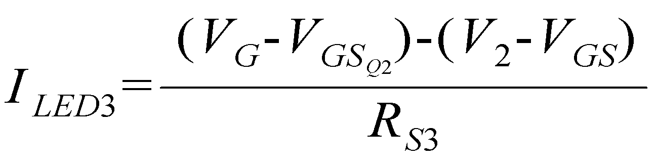
도 4의 장치에 있어서 제2 발광 다이오드(LED2)를 흐르는 두 번째 채널의 전류(![]()
![]()
![]()
![]()

여기서, ![]()
![]()
![]()
![]()
![]()
![]()
![]()
![]()
![]()
![]()
![]()
![]()
이때, 제3 트랜지스터(311) 및 제4 트랜지스터(312)로 동일한 MOSFET을 사용하는 경우에도, 상술한 수학식 1 및 수학식 2에 따라 제2 스위치 저항(314)의 저항값 및 제3 스위치 저항(315)의 저항값을 상이하게 조정함으로써 제2 발광 다이오드(LED2) 및 제3 발광 다이오드(LED3)를 입력 전압 증가에 따라 순차적으로 구동시킬 수 있다.At this time, even when the same MOSFET is used for the third transistor 311 and the
또한, 제3 트랜지스터(311) 및 제4 트랜지스터(312)로 서로 상이한 턴온 전압을 가지는 MOSFET을 사용하고, 각각 다른 레벨을 갖는 제1 구동 신호 및 제2 구동 신호로 턴온시키는 방식으로 순차적으로 구동시킬 수도 있다.In addition, the third transistor 311 and the
도 5 및 도 6에 도시된 파형에 의하면 채널 증가에 따라 도 2b와 비교하여 입력 전압(VIN)에 따른 에너지 대비 발광 다이오드의 발광에 사용되는 에너지의 비율이 증가하는 바, THD 및 효율 특성이 개선됨을 알 수 있다.According to the waveforms shown in FIGS. 5 and 6, as the channel increases, the ratio of the energy used for the light emitting diode to the light emitting diode increases compared to the energy according to the input voltage VIN as compared with FIG. 2B. .
또한, 2채널 스위칭부(400)에서 발생하는 열을 제1 구동 스위칭부(300) 또는 제2 구동 스위칭부(310)로 나누게 되어, 높은 와트로 구동하는 경우에도 고장을 방지할 수 있다.In addition, the heat generated by the two-
구동 신호 생성부(120)에 의하여 저전압인 구동 신호(![]()
![]()
![]()
![]()
![]()
![]()
이상에서 설명한 본 발명은 전술한 실시예 및 도면에 한정되는 것이 아니고, 본 발명의 기술적 사상을 벗어나지 않는 범위 내에서 얼마든지, 치환, 변경 및 변형이 가능하다는 것은 본 발명이 속하는 분야에서 통상의 지식을 가진 자에게 있어서 명백할 것이다.While the present invention has been described in connection with what is presently considered to be practical exemplary embodiments, it is to be understood that the invention is not limited to the disclosed embodiments, but, on the contrary, It will be clear to those who have.
100: 정류부
110: 브리지 다이오드
120: 제너 다이오드
200: 제1 다채널 발광 다이오드부
210: 제2 다채널 발광 다이오드부
300: 제1 구동 스위칭부
310: 제2 구동 스위칭부
320: 제3 구동 스위칭부
330: 제4 구동 스위칭부
400: 2채널 스위칭부
410: 단일 스위칭부100: rectification part
110: bridge diode
120: Zener diode
200: first multi-channel light emitting diode unit
210: a second multi-channel light emitting diode unit
300: first drive switching section
310: second drive switching unit
320: a third drive switching unit
330: fourth drive switching section
400: two-channel switching unit
410: single switching unit
Claims (11)
상기 정류부로부터 정류된 전압을 인가받아 발광하고, 적어도 제1 발광 다이오드, 제2 발광 다이오드 및 제3 발광 다이오드를 포함하는 복수개의 발광 다이오드가 직렬로 연결된 제1 다채널 발광 다이오드부;
상기 제1 다채널 발광 다이오드부에 필요한 채널 수 만큼 연결된 복수의 트랜지스터를 구비하되, 상기 제2 발광 다이오드 및 상기 제3 발광 다이오드에 연결되어, 상기 정류부에서 정류된 전압을 분배한 전압인 구동 신호를 입력받으며, 입력된 구동 신호에 따라 상기 제2 발광 다이오드 또는 상기 제3 발광 다이오드에 흐르는 전류의 경로를 스위칭하는 제1 구동 스위칭부; 및
상기 제1 발광 다이오드 및 상기 제1 구동 스위칭부에 연결되어, 제1 스위칭 전압 및 제2 스위칭 전압을 입력받아 상기 제1 발광 다이오드에 흐르는 전류 또는 상기 제1 구동 스위칭부에 흐르는 전류의 경로를 스위칭하는 2채널 스위칭부를 포함하며,
상기 2채널 스위칭부와 접지 사이에 소스 저항이 연결되고,
상기 제1 구동 스위칭부는,
게이트 단자로 상기 구동 신호를 입력받고, 드레인 단자가 상기 제2 발광 다이오드의 캐소드와 연결되며, 소스 단자가 제1 스위치 저항과 연결되어 상기 2채널 스위칭부에 연결되는 제1 트랜지스터;
게이트 단자로 상기 구동 신호를 입력받고, 드레인 단자가 상기 제3 발광 다이오드의 캐소드와 연결되며, 소스 단자가 상기 2채널 스위칭부에 연결되는 제2 트랜지스터; 및
제1 단자는 상기 제1 트랜지스터의 소스 단자에 연결되고, 제2 단자는 상기 2채널 스위칭부에 연결되어, 상기 제1 트랜지스터의 턴온 전압을 상기 제2 트랜지스터의 턴온 전압 미만으로 설정하는 제1 스위치 저항을 포함하고,
상기 2채널 스위칭부는
게이트 단자로 상기 제1 스위칭 전압을 입력받고, 드레인 단자가 상기 제1 발광 다이오드의 캐소드와 연결되며, 소스 단자가 상기 소스 저항을 통해 접지된 제1 스위치; 및
게이트 단자로 상기 제2 스위칭 전압을 입력받고, 드레인 단자가 상기 제1 스위치 저항의 제2 단자 및 제2 트랜지스터의 소스 단자와 연결되며, 소스 단자가 상기 소스 저항을 통하여 접지된 제2 스위치를 포함하는 다채널 발광 다이오드 구동 장치.
A rectifying part for receiving and rectifying the AC power supply voltage;
A first multi-channel LED unit connected in series with a plurality of light emitting diodes including at least a first light emitting diode, a second light emitting diode, and a third light emitting diode by receiving a rectified voltage from the rectifying unit;
And a plurality of transistors connected to the first multi-channel LED unit by a required number of channels, the driving signal being a voltage obtained by dividing a rectified voltage by the rectifier unit, the driving signal being connected to the second light emitting diode and the third light emitting diode, A first drive switching unit for receiving the input signal and switching a path of a current flowing in the second light emitting diode or the third light emitting diode according to an inputted drive signal; And
And a second switching unit connected to the first light emitting diode and the first driving switching unit for receiving a first switching voltage and a second switching voltage to switch a current flowing in the first light emitting diode or a current flowing in the first driving switching unit, Channel switching unit,
A source resistance is connected between the two-channel switching unit and the ground,
Wherein the first drive switching unit comprises:
A first transistor having a gate terminal receiving the driving signal, a drain terminal connected to the cathode of the second light emitting diode, and a source terminal connected to the first switch resistor and connected to the two-channel switching unit;
A second transistor having a gate terminal receiving the driving signal, a drain terminal connected to the cathode of the third light emitting diode, and a source terminal connected to the two-channel switching unit; And
The first switch is connected to the source terminal of the first transistor and the second terminal is connected to the 2-channel switching unit. The first switch sets the turn-on voltage of the first transistor to be less than the turn- Resistance,
The two-channel switching unit
A first switch receiving the first switching voltage as a gate terminal, a drain terminal connected to the cathode of the first light emitting diode, and a source terminal grounded through the source resistor; And
And a second terminal connected to the second terminal of the first switch resistor and the source terminal of the second transistor, and the source terminal includes a second switch grounded through the source resistor. Channel light emitting diode driving apparatus.
상기 정류부로부터 정류된 전압을 인가받아 발광하고, 적어도 제1 발광 다이오드, 제2 발광 다이오드, 제3 발광 다이오드 및 제4 발광 다이오드를 포함하는 복수개의 발광 다이오드가 직렬로 연결된 제2 다채널 발광 다이오드부;
상기 제2 다채널 발광 다이오드부에 필요한 채널 수 만큼 연결된 복수의 트랜지스터를 구비하되, 상기 제2 발광 다이오드, 상기 제3 발광 다이오드 및 상기 제4 발광 다이오드에 연결되어, 상기 정류부에서 정류된 전압을 분배한 전압인 구동 신호를 입력받으며, 입력된 구동 신호에 따라 상기 제2 발광 다이오드, 상기 제3 발광 다이오드 및 상기 제4 발광 다이오드에 흐르는 전류의 경로를 스위칭하는 제2 구동 스위칭부; 및
상기 제1 발광 다이오드 및 상기 제2 구동 스위칭부에 연결되어, 제1 스위칭 전압 및 제2 스위칭 전압을 입력받아 상기 제1 발광 다이오드에 흐르는 전류 또는 상기 제2 구동 스위칭부에 흐르는 전류의 경로를 스위칭하는 2채널 스위칭부를 포함하며,
상기 2채널 스위칭부와 접지 사이에 소스 저항이 연결되고,
상기 제2 구동 스위칭부는,
게이트 단자로 상기 구동 신호를 입력받고, 드레인 단자가 상기 제2 발광 다이오드의 캐소드와 연결되며, 소스 단자가 제2 스위치 저항과 연결되어 상기 2채널 스위칭부에 연결되는 제3 트랜지스터;
게이트 단자로 상기 구동 신호를 입력받고, 드레인 단자가 상기 제3 발광 다이오드의 캐소드와 연결되며, 소스 단자가 제3 스위치 저항과 연결되어 상기 2채널 스위칭부에 연결되는 제4 트랜지스터;
게이트 단자로 상기 구동 신호를 입력받고, 드레인 단자가 상기 제4 발광 다이오드의 캐소드와 연결되며, 소스 단자가 상기 2채널 스위칭부에 연결되는 제5 트랜지스터;
제1 단자는 제3 트랜지스터의 소스 단자에 연결되고, 제2 단자는 상기 2채널 스위칭부에 연결되어, 상기 제3 트랜지스터의 턴온 전압을 상기 제4 트랜지스터의 턴온 전압 및 상기 제5 트랜지스터의 턴온 전압 미만으로 설정하는 제2 스위치 저항; 및
제1 단자는 제4 트랜지스터의 소스 단자에 연결되고, 제2 단자는 상기 2채널 스위칭부에 연결되어, 상기 제4 트랜지스터의 턴온 전압을 제5 트랜지스터의 턴온 전압 미만으로 설정하는 제3 스위치 저항을 포함하고,
상기 2채널 스위칭부는,
게이트 단자로 상기 제1 스위칭 전압을 입력받고, 드레인 단자가 상기 제1 발광 다이오드의 캐소드와 연결되며, 소스 단자가 상기 소스 저항을 통해 접지된 제1 스위치; 및
게이트 단자로 상기 제2 스위칭 전압을 입력받고, 드레인 단자가 상기 제2 스위치 저항의 제2 단자, 제3 스위치 저항의 제2 단자 및 제5 트랜지스터의 소스 단자와 연결되며, 소스 단자가 상기 소스 저항을 통하여 접지된 제2 스위치를 포함하는 다채널 발광 다이오드 구동 장치.
A rectifying part for receiving and rectifying the AC power supply voltage;
And a plurality of light emitting diodes including at least a first light emitting diode, a second light emitting diode, a third light emitting diode, and a fourth light emitting diode are connected in series to each other, ;
And a plurality of transistors connected to the second multichannel LEDs by a required number of channels, wherein the second multichannel LEDs are connected to the second light emitting diode, the third light emitting diode, and the fourth light emitting diode, A second drive switching unit receiving a drive signal having a voltage and switching a path of a current flowing in the second light emitting diode, the third light emitting diode and the fourth light emitting diode according to an input drive signal; And
And a switching circuit connected to the first light emitting diode and the second driving switching part for receiving a first switching voltage and a second switching voltage and switching the current flowing in the first light emitting diode or the current flowing in the second driving switching part, Channel switching unit,
A source resistance is connected between the two-channel switching unit and the ground,
Wherein the second drive switching unit comprises:
A third transistor having a gate terminal receiving the driving signal, a drain terminal connected to the cathode of the second light emitting diode, and a source terminal connected to the second switch resistor and connected to the two-channel switching unit;
A fourth transistor having a gate terminal receiving the driving signal, a drain terminal connected to the cathode of the third light emitting diode, and a source terminal connected to the third switch resistor and connected to the two-channel switching unit;
A fifth transistor having a gate terminal receiving the driving signal, a drain terminal connected to the cathode of the fourth light emitting diode, and a source terminal connected to the two-channel switching unit;
The first terminal is connected to the source terminal of the third transistor and the second terminal is connected to the two-channel switching unit, and the turn-on voltage of the third transistor is set to a turn-on voltage of the fourth transistor and a turn- A second switch resistor for setting the second switch resistance to less than the first switch resistance; And
The third terminal is connected to the source terminal of the fourth transistor, and the second terminal is connected to the two-channel switching unit, and a third switch resistor for setting the turn-on voltage of the fourth transistor to be less than the turn- Including,
Wherein the 2-channel switching unit comprises:
A first switch receiving the first switching voltage as a gate terminal, a drain terminal connected to the cathode of the first light emitting diode, and a source terminal grounded through the source resistor; And
A source terminal connected to the second terminal of the second switch resistor, a second terminal of the third switch resistor and a source terminal of the fifth transistor, And a second switch connected between the first switch and the second switch.
상기 정류부로부터 정류된 전압을 인가받아 발광하고, 적어도 제1 발광 다이오드, 제2 발광 다이오드 및 제3 발광 다이오드를 포함하는 복수개의 발광 다이오드가 직렬로 연결된 제1 다채널 발광 다이오드부;
상기 제1 다채널 발광 다이오드부에 필요한 채널 수 만큼 연결된 복수의 트랜지스터를 구비하되, 상기 제1 발광 다이오드 및 상기 제2 발광 다이오드에 연결되어, 상기 정류부에서 정류된 전압을 분배한 전압인 구동 신호를 입력받으며, 입력된 구동 신호에 따라 상기 제1 발광 다이오드 또는 상기 제2 발광 다이오드에 흐르는 전류의 경로를 스위칭하는 제3 구동 스위칭부; 및
상기 제3 구동 스위칭부 및 상기 제3 발광 다이오드에 연결되어, 제1 스위칭 전압 및 제2 스위칭 전압을 입력받아 상기 제3 구동 스위칭부에 흐르는 전류 또는 상기 제3 발광 다이오드에 흐르는 전류의 경로를 스위칭하는 2채널 스위칭부를 포함하며,
상기 2채널 스위칭부와 접지 사이에 소스 저항이 연결되고,
상기 제3 구동 스위칭부는,
게이트 단자로 상기 구동 신호를 입력받고, 드레인 단자가 상기 제1 발광 다이오드의 캐소드와 연결되며, 소스 단자가 제1 스위치 저항과 연결되어 상기 2채널 스위칭부에 연결되는 제1 트랜지스터;
게이트 단자로 상기 구동 신호를 입력받고, 드레인 단자가 상기 제2 발광 다이오드의 캐소드와 연결되며, 소스 단자가 상기 2채널 스위칭부에 연결되는 제2 트랜지스터; 및
제1 단자는 상기 제1 트랜지스터의 소스 단자에 연결되고, 제2 단자는 상기 2채널 스위칭부에 연결되어, 상기 제1 트랜지스터의 턴온 전압을 상기 제2 트랜지스터의 턴온 전압 미만으로 설정하는 제1 스위치 저항을 포함하고,
상기 2채널 스위칭부는
게이트 단자로 상기 제1 스위칭 전압을 입력받고, 드레인 단자가 상기 제1 스위치 저항의 제2 단자 및 제2 트랜지스터의 소스 단자와 연결되며, 소스 단자가 상기 소스 저항을 통해 접지된 제1 스위치; 및
게이트 단자로 상기 제2 스위칭 전압을 입력받고, 드레인 단자가 상기 제3 발광 다이오드의 캐소드와 연결되며, 소스 단자가 상기 소스 저항을 통하여 접지된 제2 스위치를 포함하는 다채널 발광 다이오드 구동 장치.
A rectifying part for receiving and rectifying the AC power supply voltage;
A first multi-channel LED unit connected in series with a plurality of light emitting diodes including at least a first light emitting diode, a second light emitting diode, and a third light emitting diode by receiving a rectified voltage from the rectifying unit;
And a plurality of transistors connected to the first multi-channel LED unit by a required number of channels, the driving signal being a voltage obtained by dividing a rectified voltage by the rectifying unit, the driving signal being connected to the first light emitting diode and the second light emitting diode, A third drive switching unit for receiving the input signal and switching a path of a current flowing through the first light emitting diode or the second light emitting diode according to an input drive signal; And
And a third switching circuit connected to the third driving switch and the third light emitting diode for switching the path of the current flowing in the third driving switching part or the current flowing in the third light emitting diode upon receiving the first switching voltage and the second switching voltage, Channel switching unit,
A source resistance is connected between the two-channel switching unit and the ground,
Wherein the third drive switching unit comprises:
A first transistor having a gate terminal receiving the driving signal, a drain terminal connected to the cathode of the first light emitting diode, and a source terminal connected to the first switch resistor and connected to the two-channel switching unit;
A second transistor having a gate terminal receiving the driving signal, a drain terminal connected to the cathode of the second light emitting diode, and a source terminal connected to the two-channel switching unit; And
The first switch is connected to the source terminal of the first transistor and the second terminal is connected to the 2-channel switching unit. The first switch sets the turn-on voltage of the first transistor to be less than the turn- Resistance,
The two-channel switching unit
A first switch having the first switching voltage input to the gate terminal, the drain terminal connected to the second terminal of the first switch resistor and the source terminal of the second transistor, and the source terminal grounded through the source resistor; And
And a second switch having a drain terminal connected to the cathode of the third light emitting diode and a source terminal grounded through the source resistor, wherein the second switch receives the second switching voltage from the gate terminal.
상기 정류부로부터 정류된 전압을 인가받아 발광하고, 적어도 제1 발광 다이오드, 제2 발광 다이오드, 제3 발광 다이오드 및 제4 발광 다이오드를 포함하는 복수개의 발광 다이오드가 직렬로 연결된 제2 다채널 발광 다이오드부;
상기 제2 다채널 발광 다이오드부에 필요한 채널 수 만큼 연결된 복수의 트랜지스터를 구비하되, 상기 제1 발광 다이오드, 상기 제2 발광 다이오드 및 상기 제3 발광 다이오드에 연결되어, 상기 정류부에서 정류된 전압을 분배한 전압인 구동 신호를 입력받으며, 입력된 구동 신호에 따라 상기 제1 발광 다이오드, 상기 제2 발광 다이오드 및 상기 제3 발광 다이오드에 흐르는 전류의 경로를 스위칭하는 제4 구동 스위칭부; 및
상기 제4 구동 스위칭부 및 상기 제4 발광 다이오드에 연결되어, 제1 스위칭 전압 및 제2 스위칭 전압을 입력받아 상기 제4 구동 스위칭부에 흐르는 전류 또는 상기 제4 발광 다이오드에 흐르는 전류의 경로를 스위칭하는 2채널 스위칭부를 포함하며,
상기 2채널 스위칭부와 접지 사이에 소스 저항이 연결되고,
상기 제4 구동 스위칭부는,
게이트 단자로 상기 구동 신호를 입력받고, 드레인 단자가 상기 제1 발광 다이오드의 캐소드와 연결되며, 소스 단자가 제2 스위치 저항과 연결되어 상기 2채널 스위칭부에 연결되는 제3 트랜지스터;
게이트 단자로 상기 구동 신호를 입력받고, 드레인 단자가 상기 제2 발광 다이오드의 캐소드와 연결되며, 소스 단자가 제3 스위치 저항과 연결되어 상기 2채널 스위칭부에 연결되는 제4 트랜지스터;
게이트 단자로 상기 구동 신호를 입력받고, 드레인 단자가 상기 제3 발광 다이오드의 캐소드와 연결되며, 소스 단자가 상기 2채널 스위칭부에 연결되는 제5 트랜지스터;
제1 단자는 제3 트랜지스터의 소스 단자에 연결되고, 제2 단자는 상기 2채널 스위칭부에 연결되어, 상기 제3 트랜지스터의 턴온 전압을 상기 제4 트랜지스터의 턴온 전압 및 상기 제5 트랜지스터의 턴온 전압 미만으로 설정하는 제2 스위치 저항; 및
제1 단자는 제4 트랜지스터의 소스 단자에 연결되고, 제2 단자는 상기 2채널 스위칭부에 연결되어, 상기 제4 트랜지스터의 턴온 전압을 제5 트랜지스터의 턴온 전압 미만으로 설정하는 제3 스위치 저항을 포함하고,
상기 2채널 스위칭부는,
게이트 단자로 상기 제1 스위칭 전압을 입력받고, 드레인 단자가 상기 제2 스위치 저항의 제2 단자, 제3 스위치 저항의 제2 단자 및 제5 트랜지스터의 소스 단자와 연결되며, 소스 단자가 상기 소스 저항을 통해 접지된 제1 스위치; 및
게이트 단자로 상기 제2 스위칭 전압을 입력받고, 드레인 단자가 상기 제4 발광 다이오드의 캐소드와 연결되며, 소스 단자가 상기 소스 저항을 통하여 접지된 제2 스위치를 포함하는 다채널 발광 다이오드 구동 장치.
A rectifying part for receiving and rectifying the AC power supply voltage;
And a plurality of light emitting diodes including at least a first light emitting diode, a second light emitting diode, a third light emitting diode, and a fourth light emitting diode are connected in series to each other, ;
And a plurality of transistors connected to the second multichannel light emitting diode units by a required number of channels, wherein the plurality of transistors are connected to the first light emitting diode, the second light emitting diode, and the third light emitting diode, A fourth drive switching unit receiving a drive signal of one voltage and switching a path of a current flowing to the first light emitting diode, the second light emitting diode and the third light emitting diode according to an input drive signal; And
And a fourth switching circuit connected to the fourth driving switch and the fourth light emitting diode for receiving a first switching voltage and a second switching voltage and switching a path of a current flowing in the fourth driving switching part or a current flowing in the fourth light emitting diode, Channel switching unit,
A source resistance is connected between the two-channel switching unit and the ground,
Wherein the fourth drive switching unit comprises:
A third transistor having a gate terminal receiving the driving signal, a drain terminal connected to the cathode of the first light emitting diode, and a source terminal connected to the second switch resistor and connected to the two-channel switching unit;
A fourth transistor having a gate terminal receiving the driving signal, a drain terminal connected to the cathode of the second light emitting diode, and a source terminal connected to the third switch resistor and connected to the two-channel switching unit;
A fifth transistor having a gate terminal receiving the driving signal, a drain terminal connected to the cathode of the third light emitting diode, and a source terminal connected to the two-channel switching unit;
The first terminal is connected to the source terminal of the third transistor and the second terminal is connected to the two-channel switching unit, and the turn-on voltage of the third transistor is set to a turn-on voltage of the fourth transistor and a turn- A second switch resistor for setting the second switch resistance to less than the first switch resistance; And
The third terminal is connected to the source terminal of the fourth transistor, and the second terminal is connected to the two-channel switching unit, and a third switch resistor for setting the turn-on voltage of the fourth transistor to be less than the turn- Including,
Wherein the 2-channel switching unit comprises:
And a drain terminal connected to a second terminal of the second switch resistor, a second terminal of the third switch resistor, and a source terminal of the fifth transistor, and the source terminal is connected to the source resistor A first switch connected to the first switch; And
A second switch having a gate terminal connected to the second switching voltage, a drain terminal connected to the cathode of the fourth light emitting diode, and a source terminal grounded through the source resistor.
상기 정류부로부터 정류된 전압을 인가받아 발광하고, 적어도 제1 발광 다이오드, 제2 발광 다이오드 및 제3 발광 다이오드를 포함하는 복수개의 발광 다이오드가 직렬로 연결된 제1 다채널 발광 다이오드부;
상기 제1 다채널 발광 다이오드부에 필요한 채널 수 만큼 연결된 복수의 트랜지스터를 구비하되, 상기 제1 발광 다이오드, 상기 제2 발광 다이오드 및 상기 제3 발광 다이오드에 연결되어, 상기 정류부에서 정류된 전압을 분배한 전압인 구동 신호를 입력받으며, 입력된 구동 신호에 따라 상기 제1 발광 다이오드, 상기 제2 발광 다이오드 및 상기 제3 발광 다이오드에 흐르는 전류의 경로를 스위칭하는 제4 구동 스위칭부; 및
상기 제4 구동 스위칭부에 연결되어, 제1 스위칭 전압을 입력받아 상기 제4 구동 스위칭부에 흐르는 전류에 흐르는 전류의 경로를 스위칭하는 단일 스위칭부를 포함하며,
상기 단일 스위칭부와 접지 사이에 소스 저항이 연결되고,
상기 제4 구동 스위칭부는,
게이트 단자로 상기 구동 신호를 입력받고, 드레인 단자가 상기 제1 발광 다이오드의 캐소드와 연결되며, 소스 단자가 제2 스위치 저항과 연결되어 상기 단일 스위칭부에 연결되는 제3 트랜지스터;
게이트 단자로 상기 구동 신호를 입력받고, 드레인 단자가 상기 제2 발광 다이오드의 캐소드와 연결되며, 소스 단자가 제3 스위치 저항과 연결되어 상기 단일 스위칭부에 연결되는 제4 트랜지스터; 및
게이트 단자로 상기 구동 신호를 입력받고, 드레인 단자가 상기 제3 발광 다이오드의 캐소드와 연결되며, 소스 단자가 상기 단일 스위칭부에 연결되는 제5 트랜지스터;
제1 단자는 제3 트랜지스터의 소스 단자에 연결되고, 제2 단자는 상기 단일 스위칭부에 연결되어, 상기 제3 트랜지스터의 턴온 전압을 상기 제4 트랜지스터의 턴온 전압 및 상기 제5 트랜지스터의 턴온 전압 미만으로 설정하는 제2 스위치 저항; 및
제1 단자는 제4 트랜지스터의 소스 단자에 연결되고, 제2 단자는 상기 단일 스위칭부에 연결되어, 상기 제4 트랜지스터의 턴온 전압을 제5 트랜지스터의 턴온 전압 미만으로 설정하는 제3 스위치 저항을 포함하고,
상기 단일 스위칭부는,
게이트 단자로 상기 제1 스위칭 전압을 입력받고, 드레인 단자가 상기 제2 스위치 저항의 제2 단자, 제3 스위치 저항의 제2 단자 및 제5 트랜지스터의 소스 단자와 연결되며, 소스 단자가 상기 소스 저항을 통해 접지된 제1 스위치를 포함하는 다채널 발광 다이오드 구동 장치.A rectifying part for receiving and rectifying the AC power supply voltage;
A first multi-channel LED unit connected in series with a plurality of light emitting diodes including at least a first light emitting diode, a second light emitting diode, and a third light emitting diode by receiving a rectified voltage from the rectifying unit;
And a plurality of transistors connected to the first multi-channel LEDs by a required number of channels, the first LEDs being connected to the first LEDs, the second LEDs, and the third LEDs, A fourth drive switching unit receiving a drive signal of one voltage and switching a path of a current flowing to the first light emitting diode, the second light emitting diode and the third light emitting diode according to an input drive signal; And
And a single switching unit coupled to the fourth drive switching unit for receiving a first switching voltage and switching a path of a current flowing in the current flowing in the fourth driving switching unit,
A source resistor is connected between the single switching part and ground,
Wherein the fourth drive switching unit comprises:
A third transistor having a gate terminal receiving the driving signal, a drain terminal connected to the cathode of the first light emitting diode, and a source terminal connected to the second switch resistor and connected to the single switching unit;
A fourth transistor having a gate terminal receiving the driving signal, a drain terminal connected to the cathode of the second light emitting diode, and a source terminal connected to the third switch resistor and connected to the single switching unit; And
A fifth transistor having a gate terminal receiving the driving signal, a drain terminal connected to the cathode of the third light emitting diode, and a source terminal connected to the single switching unit;
The first terminal is connected to the source terminal of the third transistor and the second terminal is connected to the single switching unit so that the turn-on voltage of the third transistor is lower than the turn-on voltage of the fourth transistor and the turn- A second switch resistor for setting the first switch resistance to the second switch resistance; And
The first terminal is connected to the source terminal of the fourth transistor and the second terminal is connected to the single switching part to set the turn-on voltage of the fourth transistor to be less than the turn-on voltage of the fifth transistor and,
The single switching unit includes:
And a drain terminal connected to a second terminal of the second switch resistor, a second terminal of the third switch resistor, and a source terminal of the fifth transistor, and the source terminal is connected to the source resistor And a second switch connected between the first switch and the second switch.
Priority Applications (1)
| Application Number | Priority Date | Filing Date | Title |
|---|---|---|---|
| KR1020170064999A KR101970818B1 (en) | 2017-05-26 | 2017-05-26 | Driving apparatus for multi-channel light emitting diodes |
Applications Claiming Priority (1)
| Application Number | Priority Date | Filing Date | Title |
|---|---|---|---|
| KR1020170064999A KR101970818B1 (en) | 2017-05-26 | 2017-05-26 | Driving apparatus for multi-channel light emitting diodes |
Publications (2)
| Publication Number | Publication Date |
|---|---|
| KR20180129254A KR20180129254A (en) | 2018-12-05 |
| KR101970818B1 true KR101970818B1 (en) | 2019-04-23 |
Family
ID=64744127
Family Applications (1)
| Application Number | Title | Priority Date | Filing Date |
|---|---|---|---|
| KR1020170064999A Active KR101970818B1 (en) | 2017-05-26 | 2017-05-26 | Driving apparatus for multi-channel light emitting diodes |
Country Status (1)
| Country | Link |
|---|---|
| KR (1) | KR101970818B1 (en) |
Cited By (1)
| Publication number | Priority date | Publication date | Assignee | Title |
|---|---|---|---|---|
| US11839003B2 (en) | 2021-07-09 | 2023-12-05 | Point Tek Co., Ltd. | Apparatus for supplying power to drive alternating current (AC) direct-coupled light-emitting diodes (LED) |
Families Citing this family (1)
| Publication number | Priority date | Publication date | Assignee | Title |
|---|---|---|---|---|
| KR102193445B1 (en) * | 2020-01-22 | 2020-12-21 | 주식회사 필룩스 | Apparatus for controlling light and lighting device with the same |
Family Cites Families (2)
| Publication number | Priority date | Publication date | Assignee | Title |
|---|---|---|---|---|
| KR101610617B1 (en) * | 2013-05-23 | 2016-04-08 | 주식회사 실리콘웍스 | Led lighting apparatus |
| KR102335311B1 (en) * | 2014-11-20 | 2021-12-09 | 주식회사 엘엑스세미콘 | Lighting apparatus |
-
2017
- 2017-05-26 KR KR1020170064999A patent/KR101970818B1/en active Active
Cited By (1)
| Publication number | Priority date | Publication date | Assignee | Title |
|---|---|---|---|---|
| US11839003B2 (en) | 2021-07-09 | 2023-12-05 | Point Tek Co., Ltd. | Apparatus for supplying power to drive alternating current (AC) direct-coupled light-emitting diodes (LED) |
Also Published As
| Publication number | Publication date |
|---|---|
| KR20180129254A (en) | 2018-12-05 |
Similar Documents
| Publication | Publication Date | Title |
|---|---|---|
| US9018856B2 (en) | Light emitting diode driver having phase control mechanism | |
| CN106604444B (en) | voltage control device | |
| EP2654378A2 (en) | Led lighting apparatus driven by alternating current | |
| JP2014519687A (en) | LED light source | |
| TW201410070A (en) | Arrangement and method for driving light-emitting diodes | |
| US10111290B2 (en) | Apparatus for synchronous driving of multi-channel light emitting diodes | |
| KR102261852B1 (en) | Ac direct led driver including capacitor for led driver | |
| KR101970818B1 (en) | Driving apparatus for multi-channel light emitting diodes | |
| GB2517455A (en) | Light Apparatus | |
| KR101478782B1 (en) | LED Driving Circuit for AC Driving and Dimming Based on Constant Current of Sine Wave | |
| US11464091B2 (en) | AC direct LED driver including capacitor for LED driver | |
| KR20150031880A (en) | Apparatus for active valley-fill circuit for driving light emitting diodes | |
| KR20160001498A (en) | Led driving device capable of parallel driving of led group by voltage drop | |
| KR102003472B1 (en) | Led driving circuit and luminescence apparatus comprising the same | |
| US10880966B2 (en) | Multiple linear regulation | |
| KR102633925B1 (en) | Apparatus for supplying power to drive Alternating Current (AC) direct-coupled light-emitting diodes (LED) | |
| KR101537990B1 (en) | LED Lighting Apparatus | |
| KR102347770B1 (en) | Ac direct led driver including micro controll unit | |
| KR101984927B1 (en) | Led driving circuit and luminescence apparatus comprising the same | |
| KR101464083B1 (en) | Ac direct connection type LED driving circuit having function of flicker reduction | |
| KR101964443B1 (en) | Led driving circuit and luminescence apparatus comprising the same | |
| US11233449B2 (en) | Tapped single-stage buck converter LED driver | |
| TW201442555A (en) | Light emitting diode driving system | |
| KR20180074047A (en) | Apparatus of driving light emitting device | |
| KR102217915B1 (en) | Ac direct led driver including reference voltage source |
Legal Events
| Date | Code | Title | Description |
|---|---|---|---|
| A201 | Request for examination | ||
| PA0109 | Patent application |
Patent event code: PA01091R01D Comment text: Patent Application Patent event date: 20170526 |
|
| PA0201 | Request for examination | ||
| E902 | Notification of reason for refusal | ||
| PE0902 | Notice of grounds for rejection |
Comment text: Notification of reason for refusal Patent event date: 20180820 Patent event code: PE09021S01D |
|
| AMND | Amendment | ||
| E601 | Decision to refuse application | ||
| PE0601 | Decision on rejection of patent |
Patent event date: 20181119 Comment text: Decision to Refuse Application Patent event code: PE06012S01D Patent event date: 20180820 Comment text: Notification of reason for refusal Patent event code: PE06011S01I |
|
| PG1501 | Laying open of application | ||
| AMND | Amendment | ||
| PX0901 | Re-examination |
Patent event code: PX09011S01I Patent event date: 20181119 Comment text: Decision to Refuse Application Patent event code: PX09012R01I Patent event date: 20181018 Comment text: Amendment to Specification, etc. |
|
| PX0701 | Decision of registration after re-examination |
Patent event date: 20190116 Comment text: Decision to Grant Registration Patent event code: PX07013S01D Patent event date: 20181220 Comment text: Amendment to Specification, etc. Patent event code: PX07012R01I Patent event date: 20181119 Comment text: Decision to Refuse Application Patent event code: PX07011S01I Patent event date: 20181018 Comment text: Amendment to Specification, etc. Patent event code: PX07012R01I |
|
| X701 | Decision to grant (after re-examination) | ||
| GRNT | Written decision to grant | ||
| PR0701 | Registration of establishment |
Comment text: Registration of Establishment Patent event date: 20190415 Patent event code: PR07011E01D |
|
| PR1002 | Payment of registration fee |
Payment date: 20190416 End annual number: 3 Start annual number: 1 |
|
| PG1601 | Publication of registration | ||
| PR1001 | Payment of annual fee |
Payment date: 20220218 Start annual number: 4 End annual number: 4 |