KR101958434B1 - 유기 발광 표시 장치 - Google Patents
유기 발광 표시 장치 Download PDFInfo
- Publication number
- KR101958434B1 KR101958434B1 KR1020110089793A KR20110089793A KR101958434B1 KR 101958434 B1 KR101958434 B1 KR 101958434B1 KR 1020110089793 A KR1020110089793 A KR 1020110089793A KR 20110089793 A KR20110089793 A KR 20110089793A KR 101958434 B1 KR101958434 B1 KR 101958434B1
- Authority
- KR
- South Korea
- Prior art keywords
- pixel
- column
- pixels
- light emitting
- length
- Prior art date
- Legal status (The legal status is an assumption and is not a legal conclusion. Google has not performed a legal analysis and makes no representation as to the accuracy of the status listed.)
- Active
Links
Images


Classifications
-
- G—PHYSICS
- G09—EDUCATION; CRYPTOGRAPHY; DISPLAY; ADVERTISING; SEALS
- G09G—ARRANGEMENTS OR CIRCUITS FOR CONTROL OF INDICATING DEVICES USING STATIC MEANS TO PRESENT VARIABLE INFORMATION
- G09G3/00—Control arrangements or circuits, of interest only in connection with visual indicators other than cathode-ray tubes
- G09G3/20—Control arrangements or circuits, of interest only in connection with visual indicators other than cathode-ray tubes for presentation of an assembly of a number of characters, e.g. a page, by composing the assembly by combination of individual elements arranged in a matrix no fixed position being assigned to or needed to be assigned to the individual characters or partial characters
- G09G3/22—Control arrangements or circuits, of interest only in connection with visual indicators other than cathode-ray tubes for presentation of an assembly of a number of characters, e.g. a page, by composing the assembly by combination of individual elements arranged in a matrix no fixed position being assigned to or needed to be assigned to the individual characters or partial characters using controlled light sources
- G09G3/30—Control arrangements or circuits, of interest only in connection with visual indicators other than cathode-ray tubes for presentation of an assembly of a number of characters, e.g. a page, by composing the assembly by combination of individual elements arranged in a matrix no fixed position being assigned to or needed to be assigned to the individual characters or partial characters using controlled light sources using electroluminescent panels
- G09G3/32—Control arrangements or circuits, of interest only in connection with visual indicators other than cathode-ray tubes for presentation of an assembly of a number of characters, e.g. a page, by composing the assembly by combination of individual elements arranged in a matrix no fixed position being assigned to or needed to be assigned to the individual characters or partial characters using controlled light sources using electroluminescent panels semiconductive, e.g. using light-emitting diodes [LED]
- G09G3/3208—Control arrangements or circuits, of interest only in connection with visual indicators other than cathode-ray tubes for presentation of an assembly of a number of characters, e.g. a page, by composing the assembly by combination of individual elements arranged in a matrix no fixed position being assigned to or needed to be assigned to the individual characters or partial characters using controlled light sources using electroluminescent panels semiconductive, e.g. using light-emitting diodes [LED] organic, e.g. using organic light-emitting diodes [OLED]
- G09G3/3225—Control arrangements or circuits, of interest only in connection with visual indicators other than cathode-ray tubes for presentation of an assembly of a number of characters, e.g. a page, by composing the assembly by combination of individual elements arranged in a matrix no fixed position being assigned to or needed to be assigned to the individual characters or partial characters using controlled light sources using electroluminescent panels semiconductive, e.g. using light-emitting diodes [LED] organic, e.g. using organic light-emitting diodes [OLED] using an active matrix
-
- H—ELECTRICITY
- H10—SEMICONDUCTOR DEVICES; ELECTRIC SOLID-STATE DEVICES NOT OTHERWISE PROVIDED FOR
- H10K—ORGANIC ELECTRIC SOLID-STATE DEVICES
- H10K50/00—Organic light-emitting devices
- H10K50/80—Constructional details
- H10K50/805—Electrodes
-
- H—ELECTRICITY
- H10—SEMICONDUCTOR DEVICES; ELECTRIC SOLID-STATE DEVICES NOT OTHERWISE PROVIDED FOR
- H10K—ORGANIC ELECTRIC SOLID-STATE DEVICES
- H10K59/00—Integrated devices, or assemblies of multiple devices, comprising at least one organic light-emitting element covered by group H10K50/00
- H10K59/30—Devices specially adapted for multicolour light emission
- H10K59/35—Devices specially adapted for multicolour light emission comprising red-green-blue [RGB] subpixels
- H10K59/352—Devices specially adapted for multicolour light emission comprising red-green-blue [RGB] subpixels the areas of the RGB subpixels being different
-
- H—ELECTRICITY
- H10—SEMICONDUCTOR DEVICES; ELECTRIC SOLID-STATE DEVICES NOT OTHERWISE PROVIDED FOR
- H10K—ORGANIC ELECTRIC SOLID-STATE DEVICES
- H10K59/00—Integrated devices, or assemblies of multiple devices, comprising at least one organic light-emitting element covered by group H10K50/00
- H10K59/30—Devices specially adapted for multicolour light emission
- H10K59/35—Devices specially adapted for multicolour light emission comprising red-green-blue [RGB] subpixels
- H10K59/353—Devices specially adapted for multicolour light emission comprising red-green-blue [RGB] subpixels characterised by the geometrical arrangement of the RGB subpixels
-
- G—PHYSICS
- G09—EDUCATION; CRYPTOGRAPHY; DISPLAY; ADVERTISING; SEALS
- G09G—ARRANGEMENTS OR CIRCUITS FOR CONTROL OF INDICATING DEVICES USING STATIC MEANS TO PRESENT VARIABLE INFORMATION
- G09G2300/00—Aspects of the constitution of display devices
- G09G2300/04—Structural and physical details of display devices
- G09G2300/0439—Pixel structures
- G09G2300/0452—Details of colour pixel setup, e.g. pixel composed of a red, a blue and two green components
-
- G—PHYSICS
- G09—EDUCATION; CRYPTOGRAPHY; DISPLAY; ADVERTISING; SEALS
- G09G—ARRANGEMENTS OR CIRCUITS FOR CONTROL OF INDICATING DEVICES USING STATIC MEANS TO PRESENT VARIABLE INFORMATION
- G09G2300/00—Aspects of the constitution of display devices
- G09G2300/04—Structural and physical details of display devices
- G09G2300/0439—Pixel structures
- G09G2300/0465—Improved aperture ratio, e.g. by size reduction of the pixel circuit, e.g. for improving the pixel density or the maximum displayable luminance or brightness
Landscapes
- Engineering & Computer Science (AREA)
- Physics & Mathematics (AREA)
- Computer Hardware Design (AREA)
- General Physics & Mathematics (AREA)
- Theoretical Computer Science (AREA)
- Optics & Photonics (AREA)
- Electroluminescent Light Sources (AREA)
Abstract
Description
도 2는 본 발명의 제1 실시예에 따른 유기 발광 표시 장치의 단면도이다.
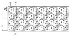
도 3은 본 발명의 제1 실시예에 따른 유기 발광 표시 장치의 복수개의 화소의 배열 구조를 도시한 평면도이다.
도 4 내지 도 7은 본 발명의 제1 실시예에 따른 유기 발광 표시 장치의 구동 방법을 나타낸 도면이다.
도 8은 본 발명의 제1 실시예에 따른 유기 발광 표시 장치와 비교예 1 및 비교예 2의 해상도에 따른 개구율의 관계를 도시한 그래프이다.
도 9는 본 발명의 제2 실시예에 따른 유기 발광 표시 장치의 복수개의 화소의 배열 구조를 도시한 평면도이다.
도 10은 본 발명의 제3 실시예에 따른 유기 발광 표시 장치의 복수개의 화소의 배열 구조를 도시한 평면도이다.
도 11은 본 발명의 제4 실시예에 따른 유기 발광 표시 장치의 복수개의 화소의 배열 구조를 도시한 평면도이다.
도 12는 본 발명의 제5 실시예에 따른 유기 발광 표시 장치의 복수개의 화소의 배열 구조를 도시한 평면도이다.
30: 제3 화소 190: 화소 전극
270: 공통 전극 320: 유기 발광층
400: 박막 봉지층
Claims (13)
- 동일한 제1 열을 따라 교대로 배치되어 있는 제1 화소 및 제2 화소,
상기 제1 열에 인접한 제2 열을 따라 배치되어 있는 제3 화소
를 포함하고,
상기 제1 열에 배치된 하나의 상기 제1 화소의 열방향 길이와 하나의 상기 제2 화소의 열방향 길이의 합이 상기 제2 열에 배치된 3개 내지 5개의 상기 제3 화소의 열방향 길이의 합과 동일하고,
하나의 상기 제2 화소에 인접한 4개의 상기 제1 화소는 하나의 상기 제2 화소를 마름모 형상으로 둘러싸고, 하나의 상기 제1 화소에 인접한 4개의 상기 제2 화소는 하나의 상기 제1 화소를 마름모 형상으로 둘러싸며,
상기 제1 화소, 제2 화소 및 제3 화소는 각각 적색 화소, 청색 화소 및 녹색 화소이며,
하나의 제3 화소에 인접한 하나의 상기 제1 화소 또는 하나의 상기 제2 화소는 상기 하나의 제3 화소와 동일한 휘도로 구동되고, 상기 제2 화소를 마름모 형상으로 둘러싸는 상기 제1 화소 또는 상기 제1 화소를 마름모 형상으로 둘러싸는 상기 제2 화소가 구동되는 유기 발광 표시 장치. - 삭제
- 제1항에 있어서,
상기 제1 화소의 열방향 길이와 상기 제2 화소의 열방향 길이는 서로 동일한 유기 발광 표시 장치. - 삭제
- 제1항에 있어서,
상기 제1 열에 배치된 상기 제1 화소 및 제2 화소는 상기 제1 화소 및 제2 화소의 순서대로 교대로 배치되고,
상기 제2 열에 인접한 제3 열에 배치된 상기 제1 화소 및 제2 화소는 상기 제2 화소 및 제1 화소의 순서대로 교대로 배치되어 있는 유기 발광 표시 장치. - 제5항에 있어서,
상기 제1 열과 상기 제2 열을 포함하는 제1 화소 열과,
상기 제3 열과 상기 제3 열에 인접하며 상기 제3 화소가 배치된 제4 열을 포함하는 제2 화소 열은 행방향으로 교대로 배치되어 있는 유기 발광 표시 장치. - 제5항에 있어서,
상기 제1 열에 배치된 상기 제1 화소와 상기 제3 열에 배치된 상기 제1 화소는 상기 제2 열에 배치된 상기 제3 화소를 기준으로 대각선 방향으로 서로 배치되어 있고,
상기 제1 열에 배치된 상기 제2 화소와 상기 제3 열에 배치된 상기 제2 화소는 상기 제2 열에 배치된 상기 제3 화소를 기준으로 대각선 방향으로 서로 배치되어 있는 유기 발광 표시 장치. - 삭제
- 삭제
- 삭제
- 삭제
- 제1항에 있어서,
상기 하나의 제1 화소와 상기 하나의 제2 화소의 면적은 서로 동일한 유기 발광 표시 장치. - 제12항에 있어서,
상기 제2 화소와 상기 제3 화소의 면적은 서로 다른 유기 발광 표시 장치.
Priority Applications (3)
| Application Number | Priority Date | Filing Date | Title |
|---|---|---|---|
| KR1020110089793A KR101958434B1 (ko) | 2011-09-05 | 2011-09-05 | 유기 발광 표시 장치 |
| US13/469,036 US10199437B2 (en) | 2011-09-05 | 2012-05-10 | Organic light emitting diode display |
| US16/252,340 US10840306B2 (en) | 2011-09-05 | 2019-01-18 | Organic light emitting diode display |
Applications Claiming Priority (1)
| Application Number | Priority Date | Filing Date | Title |
|---|---|---|---|
| KR1020110089793A KR101958434B1 (ko) | 2011-09-05 | 2011-09-05 | 유기 발광 표시 장치 |
Publications (2)
| Publication Number | Publication Date |
|---|---|
| KR20130026628A KR20130026628A (ko) | 2013-03-14 |
| KR101958434B1 true KR101958434B1 (ko) | 2019-03-15 |
Family
ID=47752777
Family Applications (1)
| Application Number | Title | Priority Date | Filing Date |
|---|---|---|---|
| KR1020110089793A Active KR101958434B1 (ko) | 2011-09-05 | 2011-09-05 | 유기 발광 표시 장치 |
Country Status (2)
| Country | Link |
|---|---|
| US (2) | US10199437B2 (ko) |
| KR (1) | KR101958434B1 (ko) |
Families Citing this family (43)
| Publication number | Priority date | Publication date | Assignee | Title |
|---|---|---|---|---|
| US10832616B2 (en) | 2012-03-06 | 2020-11-10 | Samsung Display Co., Ltd. | Pixel arrangement structure for organic light emitting diode display |
| KR101615332B1 (ko) | 2012-03-06 | 2016-04-26 | 삼성디스플레이 주식회사 | 유기 발광 표시 장치의 화소 배열 구조 |
| KR101485166B1 (ko) * | 2013-04-25 | 2015-01-22 | 삼성디스플레이 주식회사 | 유기 발광 표시 장치 및 마스크 유닛 |
| KR101427593B1 (ko) | 2013-04-26 | 2014-08-07 | 삼성디스플레이 주식회사 | 유기 발광 표시 장치 |
| KR102231279B1 (ko) | 2013-10-30 | 2021-03-25 | 삼성디스플레이 주식회사 | 영상 데이터 인코딩 장치 및 방법 |
| KR102253039B1 (ko) | 2013-11-04 | 2021-05-20 | 삼성디스플레이 주식회사 | 영상 데이터 인코딩 장치 및 방법 |
| KR102271226B1 (ko) * | 2013-11-13 | 2021-06-29 | 엘지디스플레이 주식회사 | 유기발광표시패널 및 이를 이용한 유기발광표시장치 |
| TWI545749B (zh) | 2014-04-23 | 2016-08-11 | 群創光電股份有限公司 | 顯示基板及應用其之顯示裝置 |
| CN105006479B (zh) * | 2014-04-23 | 2018-04-20 | 群创光电股份有限公司 | 显示基板及应用其的显示装置 |
| CN103985735A (zh) * | 2014-04-25 | 2014-08-13 | 友达光电股份有限公司 | 一种显示面板 |
| KR102215092B1 (ko) * | 2014-06-05 | 2021-02-15 | 삼성디스플레이 주식회사 | 유기 발광 표시 장치 |
| KR102239160B1 (ko) | 2014-11-10 | 2021-04-13 | 삼성디스플레이 주식회사 | 표시장치 및 그 구동 방법 |
| CN104465706A (zh) * | 2014-12-17 | 2015-03-25 | 上海天马有机发光显示技术有限公司 | 一种有机发光显示装置及其制作方法 |
| CN105789249B (zh) * | 2014-12-25 | 2018-09-11 | 昆山国显光电有限公司 | 像素结构和采用该像素结构的有机发光显示装置 |
| KR102282030B1 (ko) | 2015-01-26 | 2021-07-29 | 삼성디스플레이 주식회사 | 표시 장치 |
| US9780150B2 (en) | 2015-02-16 | 2017-10-03 | Shanghai Tianma AM-OLED Co., Ltd. | Organic light emitting diode display device and manufacturing method thereof |
| CN105139764B (zh) * | 2015-09-23 | 2018-02-06 | 厦门天马微电子有限公司 | 显示装置及显示方法 |
| KR102735234B1 (ko) * | 2016-04-30 | 2024-11-27 | 엘지디스플레이 주식회사 | 유기발광 표시장치용 기판 및 유기발광 표시장치 |
| CN105427806B (zh) * | 2016-01-06 | 2018-10-23 | 京东方科技集团股份有限公司 | 像素电路、显示基板及显示装置、驱动显示基板的方法 |
| CN105976757B (zh) * | 2016-07-26 | 2019-01-18 | 京东方科技集团股份有限公司 | 像素排列结构、像素电路、显示面板及驱动方法 |
| KR102714947B1 (ko) * | 2016-08-31 | 2024-10-07 | 엘지디스플레이 주식회사 | 유기 발광 표시 장치 |
| KR102597681B1 (ko) | 2016-09-19 | 2023-11-06 | 삼성디스플레이 주식회사 | 표시 장치 |
| CN107968103B (zh) * | 2016-10-20 | 2020-03-17 | 昆山国显光电有限公司 | 像素结构及其制造方法、显示装置 |
| KR102743728B1 (ko) | 2016-11-08 | 2024-12-19 | 삼성디스플레이 주식회사 | 표시 장치 |
| JP6755809B2 (ja) * | 2017-01-23 | 2020-09-16 | 株式会社ジャパンディスプレイ | 表示装置 |
| CN108538882B (zh) * | 2017-03-02 | 2020-05-19 | 京东方科技集团股份有限公司 | 显示面板及显示装置 |
| KR102411145B1 (ko) * | 2017-04-19 | 2022-06-20 | 삼성디스플레이 주식회사 | 헤드 마운티드 디스플레이 장치 |
| CN109036257B (zh) * | 2018-10-24 | 2022-04-29 | 上海天马微电子有限公司 | 一种显示面板及其驱动方法和显示装置 |
| CN208753326U (zh) * | 2018-11-05 | 2019-04-16 | 北京京东方技术开发有限公司 | 显示基板和显示装置 |
| CN109634011B (zh) * | 2019-01-08 | 2022-01-07 | 昆山国显光电有限公司 | 阵列基板、显示面板和显示装置 |
| KR20200106589A (ko) | 2019-03-04 | 2020-09-15 | 삼성디스플레이 주식회사 | 표시 장치, 표시 장치의 제조장치 및 표시 장치의 제조방법 |
| US11562689B2 (en) * | 2019-03-25 | 2023-01-24 | Sharp Kabushiki Kaisha | Display device |
| CN110112189B (zh) * | 2019-04-25 | 2021-03-23 | 武汉华星光电半导体显示技术有限公司 | 显示面板及显示装置 |
| CN110364557B (zh) * | 2019-07-10 | 2021-09-14 | 云谷(固安)科技有限公司 | 像素排布结构及显示面板 |
| KR102663897B1 (ko) | 2019-07-10 | 2024-05-08 | 삼성디스플레이 주식회사 | 표시 장치 |
| CN110364558B (zh) * | 2019-07-15 | 2021-11-16 | 云谷(固安)科技有限公司 | 像素排布结构及显示面板 |
| CN110599954B (zh) * | 2019-08-02 | 2021-09-07 | 北京集创北方科技股份有限公司 | 子像素渲染方法和显示驱动装置 |
| US11056081B2 (en) * | 2019-08-09 | 2021-07-06 | Wuhan China Star Optoelectronics Semiconductor Display Technology Co., Ltd. | Display panel and display device |
| US11557635B2 (en) * | 2019-12-10 | 2023-01-17 | Samsung Display Co., Ltd. | Display device, mask assembly, and apparatus for manufacturing the display device |
| KR102379744B1 (ko) * | 2019-12-20 | 2022-03-29 | 삼성디스플레이 주식회사 | 디스플레이 패널 및 이를 포함하는 디스플레이 장치 |
| WO2021217676A1 (zh) * | 2020-04-30 | 2021-11-04 | 华为技术有限公司 | 显示面板、显示终端与显示装置 |
| KR20220096188A (ko) * | 2020-12-30 | 2022-07-07 | 엘지디스플레이 주식회사 | 표시 장치 |
| CN116940974A (zh) * | 2021-09-30 | 2023-10-24 | 京东方科技集团股份有限公司 | 显示面板及显示装置 |
Citations (1)
| Publication number | Priority date | Publication date | Assignee | Title |
|---|---|---|---|---|
| US20050099540A1 (en) * | 2003-10-28 | 2005-05-12 | Elliott Candice H.B. | Display system having improved multiple modes for displaying image data from multiple input source formats |
Family Cites Families (15)
| Publication number | Priority date | Publication date | Assignee | Title |
|---|---|---|---|---|
| US5504504A (en) * | 1994-07-13 | 1996-04-02 | Texas Instruments Incorporated | Method of reducing the visual impact of defects present in a spatial light modulator display |
| US5899550A (en) * | 1996-08-26 | 1999-05-04 | Canon Kabushiki Kaisha | Display device having different arrangements of larger and smaller sub-color pixels |
| US6750875B1 (en) * | 1999-02-01 | 2004-06-15 | Microsoft Corporation | Compression of image data associated with two-dimensional arrays of pixel sub-components |
| US6666446B2 (en) * | 2001-06-13 | 2003-12-23 | Hewlett-Packard Development Company, L.P. | Replaceable roller bogie for document feeding apparatus |
| JP3870807B2 (ja) * | 2001-12-20 | 2007-01-24 | ソニー株式会社 | 画像表示装置及びその製造方法 |
| KR100885842B1 (ko) | 2002-08-08 | 2009-02-27 | 엘지디스플레이 주식회사 | 유기 전계 발광 표시소자 및 그 제조방법 |
| JP2005222928A (ja) * | 2004-01-07 | 2005-08-18 | Seiko Epson Corp | 電気光学装置 |
| KR100688801B1 (ko) * | 2004-11-22 | 2007-03-02 | 삼성에스디아이 주식회사 | 델타 화소회로 및 발광 표시장치 |
| JP4305437B2 (ja) | 2005-05-19 | 2009-07-29 | エプソンイメージングデバイス株式会社 | 電気光学装置及び電子機器 |
| US7898623B2 (en) * | 2005-07-04 | 2011-03-01 | Semiconductor Energy Laboratory Co., Ltd. | Display device, electronic device and method of driving display device |
| JP5403860B2 (ja) * | 2006-10-10 | 2014-01-29 | 株式会社ジャパンディスプレイ | カラー液晶表示装置 |
| KR101499234B1 (ko) * | 2008-06-27 | 2015-03-05 | 삼성디스플레이 주식회사 | 유기 발광 표시 장치, 그 제조 방법 및 이에 사용되는섀도우 마스크 |
| US20100109562A1 (en) | 2008-11-06 | 2010-05-06 | StarChips Technology Inc. | Backlight module and light-emitting device thereof |
| KR101568262B1 (ko) | 2009-09-08 | 2015-11-12 | 엘지디스플레이 주식회사 | 4색 서브화소를 갖는 액정 표시 장치 |
| KR101189025B1 (ko) * | 2010-05-31 | 2012-10-08 | 삼성디스플레이 주식회사 | 유기전계발광 표시장치의 화소배열구조 |
-
2011
- 2011-09-05 KR KR1020110089793A patent/KR101958434B1/ko active Active
-
2012
- 2012-05-10 US US13/469,036 patent/US10199437B2/en active Active
-
2019
- 2019-01-18 US US16/252,340 patent/US10840306B2/en active Active
Patent Citations (1)
| Publication number | Priority date | Publication date | Assignee | Title |
|---|---|---|---|---|
| US20050099540A1 (en) * | 2003-10-28 | 2005-05-12 | Elliott Candice H.B. | Display system having improved multiple modes for displaying image data from multiple input source formats |
Also Published As
| Publication number | Publication date |
|---|---|
| US10199437B2 (en) | 2019-02-05 |
| KR20130026628A (ko) | 2013-03-14 |
| US10840306B2 (en) | 2020-11-17 |
| US20190172877A1 (en) | 2019-06-06 |
| US20130057521A1 (en) | 2013-03-07 |
Similar Documents
| Publication | Publication Date | Title |
|---|---|---|
| KR101958434B1 (ko) | 유기 발광 표시 장치 | |
| US11864425B2 (en) | Electroluminescent display device having large size and high definition | |
| KR101900914B1 (ko) | 유기 발광 표시 장치 | |
| KR100834346B1 (ko) | 능동행렬 유기전기발광소자 | |
| US9972663B2 (en) | Organic light emitting display device including driving sub-pixels each overlapping with multiple color sub-pixels | |
| KR102124043B1 (ko) | 화소 배열 구조 및 이를 채용하는 표시 장치 | |
| KR100473591B1 (ko) | 듀얼패널타입 유기전계발광 소자 및 그의 제조방법 | |
| KR102127410B1 (ko) | 유기 발광 표시 장치 및 그 제조 방법 | |
| US7626329B2 (en) | Organic electroluminescent device with black insulator | |
| KR100461467B1 (ko) | 능동행렬 유기전기발광소자 | |
| US20130056784A1 (en) | Organic Light-Emitting Display Device and Method of Fabricating the Same | |
| US20150009104A1 (en) | Organic light-emitting diode (oled) display | |
| US8330353B2 (en) | Organic light emitting device and manufacturing method thereof | |
| US11367377B2 (en) | Display device | |
| KR20200066959A (ko) | 투명표시장치 | |
| KR20190047235A (ko) | 유기 발광 표시 장치 | |
| US20120133272A1 (en) | Organic el display apparatus | |
| KR20140021398A (ko) | 유기 발광 표시 장치 | |
| KR20140129852A (ko) | 유기 발광 표시 장치 | |
| KR20210085331A (ko) | 전계발광 표시장치 | |
| KR100474001B1 (ko) | 듀얼패널타입 유기전계발광 소자 및 그의 제조방법 | |
| KR20100068074A (ko) | 유기 발광 표시 장치 | |
| KR100683403B1 (ko) | 유기전계발광소자 및 그 제조 방법 | |
| KR102609087B1 (ko) | 유기발광소자 | |
| KR100474000B1 (ko) | 듀얼패널타입 유기전계발광 소자 및 그의 제조방법 |
Legal Events
| Date | Code | Title | Description |
|---|---|---|---|
| PA0109 | Patent application |
Patent event code: PA01091R01D Comment text: Patent Application Patent event date: 20110905 |
|
| N231 | Notification of change of applicant | ||
| PN2301 | Change of applicant |
Patent event date: 20120726 Comment text: Notification of Change of Applicant Patent event code: PN23011R01D |
|
| PG1501 | Laying open of application | ||
| A201 | Request for examination | ||
| PA0201 | Request for examination |
Patent event code: PA02012R01D Patent event date: 20160902 Comment text: Request for Examination of Application Patent event code: PA02011R01I Patent event date: 20110905 Comment text: Patent Application |
|
| E902 | Notification of reason for refusal | ||
| PE0902 | Notice of grounds for rejection |
Comment text: Notification of reason for refusal Patent event date: 20180426 Patent event code: PE09021S01D |
|
| AMND | Amendment | ||
| E601 | Decision to refuse application | ||
| PE0601 | Decision on rejection of patent |
Patent event date: 20181029 Comment text: Decision to Refuse Application Patent event code: PE06012S01D Patent event date: 20180426 Comment text: Notification of reason for refusal Patent event code: PE06011S01I |
|
| AMND | Amendment | ||
| PX0901 | Re-examination |
Patent event code: PX09011S01I Patent event date: 20181029 Comment text: Decision to Refuse Application Patent event code: PX09012R01I Patent event date: 20180626 Comment text: Amendment to Specification, etc. |
|
| PX0701 | Decision of registration after re-examination |
Patent event date: 20181212 Comment text: Decision to Grant Registration Patent event code: PX07013S01D Patent event date: 20181129 Comment text: Amendment to Specification, etc. Patent event code: PX07012R01I Patent event date: 20181029 Comment text: Decision to Refuse Application Patent event code: PX07011S01I Patent event date: 20180626 Comment text: Amendment to Specification, etc. Patent event code: PX07012R01I |
|
| X701 | Decision to grant (after re-examination) | ||
| PR0701 | Registration of establishment |
Comment text: Registration of Establishment Patent event date: 20190308 Patent event code: PR07011E01D |
|
| PR1002 | Payment of registration fee |
Payment date: 20190308 End annual number: 3 Start annual number: 1 |
|
| PG1601 | Publication of registration | ||
| PR1001 | Payment of annual fee |
Payment date: 20220302 Start annual number: 4 End annual number: 4 |
|
| PR1001 | Payment of annual fee |
Payment date: 20250224 Start annual number: 7 End annual number: 7 |