KR101929452B1 - Display apparatus - Google Patents
Display apparatus Download PDFInfo
- Publication number
- KR101929452B1 KR101929452B1 KR1020160097459A KR20160097459A KR101929452B1 KR 101929452 B1 KR101929452 B1 KR 101929452B1 KR 1020160097459 A KR1020160097459 A KR 1020160097459A KR 20160097459 A KR20160097459 A KR 20160097459A KR 101929452 B1 KR101929452 B1 KR 101929452B1
- Authority
- KR
- South Korea
- Prior art keywords
- layer
- region
- disposed
- insulating layer
- organic
- Prior art date
- Legal status (The legal status is an assumption and is not a legal conclusion. Google has not performed a legal analysis and makes no representation as to the accuracy of the status listed.)
- Active
Links
Images


Classifications
-
- G—PHYSICS
- G06—COMPUTING OR CALCULATING; COUNTING
- G06F—ELECTRIC DIGITAL DATA PROCESSING
- G06F3/00—Input arrangements for transferring data to be processed into a form capable of being handled by the computer; Output arrangements for transferring data from processing unit to output unit, e.g. interface arrangements
- G06F3/01—Input arrangements or combined input and output arrangements for interaction between user and computer
- G06F3/03—Arrangements for converting the position or the displacement of a member into a coded form
- G06F3/041—Digitisers, e.g. for touch screens or touch pads, characterised by the transducing means
- G06F3/0412—Digitisers structurally integrated in a display
-
- H01L51/5246—
-
- H—ELECTRICITY
- H10—SEMICONDUCTOR DEVICES; ELECTRIC SOLID-STATE DEVICES NOT OTHERWISE PROVIDED FOR
- H10K—ORGANIC ELECTRIC SOLID-STATE DEVICES
- H10K50/00—Organic light-emitting devices
- H10K50/80—Constructional details
- H10K50/84—Passivation; Containers; Encapsulations
- H10K50/842—Containers
- H10K50/8426—Peripheral sealing arrangements, e.g. adhesives, sealants
-
- G—PHYSICS
- G06—COMPUTING OR CALCULATING; COUNTING
- G06F—ELECTRIC DIGITAL DATA PROCESSING
- G06F3/00—Input arrangements for transferring data to be processed into a form capable of being handled by the computer; Output arrangements for transferring data from processing unit to output unit, e.g. interface arrangements
- G06F3/01—Input arrangements or combined input and output arrangements for interaction between user and computer
- G06F3/03—Arrangements for converting the position or the displacement of a member into a coded form
- G06F3/041—Digitisers, e.g. for touch screens or touch pads, characterised by the transducing means
- G06F3/0416—Control or interface arrangements specially adapted for digitisers
- G06F3/04164—Connections between sensors and controllers, e.g. routing lines between electrodes and connection pads
-
- G—PHYSICS
- G06—COMPUTING OR CALCULATING; COUNTING
- G06F—ELECTRIC DIGITAL DATA PROCESSING
- G06F3/00—Input arrangements for transferring data to be processed into a form capable of being handled by the computer; Output arrangements for transferring data from processing unit to output unit, e.g. interface arrangements
- G06F3/01—Input arrangements or combined input and output arrangements for interaction between user and computer
- G06F3/03—Arrangements for converting the position or the displacement of a member into a coded form
- G06F3/041—Digitisers, e.g. for touch screens or touch pads, characterised by the transducing means
- G06F3/044—Digitisers, e.g. for touch screens or touch pads, characterised by the transducing means by capacitive means
- G06F3/0443—Digitisers, e.g. for touch screens or touch pads, characterised by the transducing means by capacitive means using a single layer of sensing electrodes
-
- G—PHYSICS
- G06—COMPUTING OR CALCULATING; COUNTING
- G06F—ELECTRIC DIGITAL DATA PROCESSING
- G06F3/00—Input arrangements for transferring data to be processed into a form capable of being handled by the computer; Output arrangements for transferring data from processing unit to output unit, e.g. interface arrangements
- G06F3/01—Input arrangements or combined input and output arrangements for interaction between user and computer
- G06F3/03—Arrangements for converting the position or the displacement of a member into a coded form
- G06F3/041—Digitisers, e.g. for touch screens or touch pads, characterised by the transducing means
- G06F3/044—Digitisers, e.g. for touch screens or touch pads, characterised by the transducing means by capacitive means
- G06F3/0446—Digitisers, e.g. for touch screens or touch pads, characterised by the transducing means by capacitive means using a grid-like structure of electrodes in at least two directions, e.g. using row and column electrodes
-
- H01L27/3223—
-
- H01L27/323—
-
- H01L27/3244—
-
- H01L51/0097—
-
- H01L51/5253—
-
- H—ELECTRICITY
- H10—SEMICONDUCTOR DEVICES; ELECTRIC SOLID-STATE DEVICES NOT OTHERWISE PROVIDED FOR
- H10K—ORGANIC ELECTRIC SOLID-STATE DEVICES
- H10K10/00—Organic devices specially adapted for rectifying, amplifying, oscillating or switching; Organic capacitors or resistors having potential barriers
- H10K10/40—Organic transistors
- H10K10/46—Field-effect transistors, e.g. organic thin-film transistors [OTFT]
- H10K10/462—Insulated gate field-effect transistors [IGFETs]
- H10K10/468—Insulated gate field-effect transistors [IGFETs] characterised by the gate dielectrics
- H10K10/474—Insulated gate field-effect transistors [IGFETs] characterised by the gate dielectrics the gate dielectric comprising a multilayered structure
- H10K10/476—Insulated gate field-effect transistors [IGFETs] characterised by the gate dielectrics the gate dielectric comprising a multilayered structure comprising at least one organic layer and at least one inorganic layer
-
- H—ELECTRICITY
- H10—SEMICONDUCTOR DEVICES; ELECTRIC SOLID-STATE DEVICES NOT OTHERWISE PROVIDED FOR
- H10K—ORGANIC ELECTRIC SOLID-STATE DEVICES
- H10K10/00—Organic devices specially adapted for rectifying, amplifying, oscillating or switching; Organic capacitors or resistors having potential barriers
- H10K10/80—Constructional details
- H10K10/88—Passivation; Containers; Encapsulations
-
- H—ELECTRICITY
- H10—SEMICONDUCTOR DEVICES; ELECTRIC SOLID-STATE DEVICES NOT OTHERWISE PROVIDED FOR
- H10K—ORGANIC ELECTRIC SOLID-STATE DEVICES
- H10K50/00—Organic light-emitting devices
- H10K50/80—Constructional details
- H10K50/84—Passivation; Containers; Encapsulations
- H10K50/844—Encapsulations
-
- H—ELECTRICITY
- H10—SEMICONDUCTOR DEVICES; ELECTRIC SOLID-STATE DEVICES NOT OTHERWISE PROVIDED FOR
- H10K—ORGANIC ELECTRIC SOLID-STATE DEVICES
- H10K59/00—Integrated devices, or assemblies of multiple devices, comprising at least one organic light-emitting element covered by group H10K50/00
- H10K59/10—OLED displays
- H10K59/12—Active-matrix OLED [AMOLED] displays
-
- H—ELECTRICITY
- H10—SEMICONDUCTOR DEVICES; ELECTRIC SOLID-STATE DEVICES NOT OTHERWISE PROVIDED FOR
- H10K—ORGANIC ELECTRIC SOLID-STATE DEVICES
- H10K59/00—Integrated devices, or assemblies of multiple devices, comprising at least one organic light-emitting element covered by group H10K50/00
- H10K59/40—OLEDs integrated with touch screens
-
- H—ELECTRICITY
- H10—SEMICONDUCTOR DEVICES; ELECTRIC SOLID-STATE DEVICES NOT OTHERWISE PROVIDED FOR
- H10K—ORGANIC ELECTRIC SOLID-STATE DEVICES
- H10K59/00—Integrated devices, or assemblies of multiple devices, comprising at least one organic light-emitting element covered by group H10K50/00
- H10K59/80—Constructional details
- H10K59/87—Passivation; Containers; Encapsulations
- H10K59/873—Encapsulations
-
- H—ELECTRICITY
- H10—SEMICONDUCTOR DEVICES; ELECTRIC SOLID-STATE DEVICES NOT OTHERWISE PROVIDED FOR
- H10K—ORGANIC ELECTRIC SOLID-STATE DEVICES
- H10K59/00—Integrated devices, or assemblies of multiple devices, comprising at least one organic light-emitting element covered by group H10K50/00
- H10K59/80—Constructional details
- H10K59/88—Dummy elements, i.e. elements having non-functional features
-
- H—ELECTRICITY
- H10—SEMICONDUCTOR DEVICES; ELECTRIC SOLID-STATE DEVICES NOT OTHERWISE PROVIDED FOR
- H10K—ORGANIC ELECTRIC SOLID-STATE DEVICES
- H10K71/00—Manufacture or treatment specially adapted for the organic devices covered by this subclass
- H10K71/621—Providing a shape to conductive layers, e.g. patterning or selective deposition
-
- H—ELECTRICITY
- H10—SEMICONDUCTOR DEVICES; ELECTRIC SOLID-STATE DEVICES NOT OTHERWISE PROVIDED FOR
- H10K—ORGANIC ELECTRIC SOLID-STATE DEVICES
- H10K71/00—Manufacture or treatment specially adapted for the organic devices covered by this subclass
- H10K71/821—Patterning of a layer by embossing, e.g. stamping to form trenches in an insulating layer
-
- H—ELECTRICITY
- H10—SEMICONDUCTOR DEVICES; ELECTRIC SOLID-STATE DEVICES NOT OTHERWISE PROVIDED FOR
- H10K—ORGANIC ELECTRIC SOLID-STATE DEVICES
- H10K77/00—Constructional details of devices covered by this subclass and not covered by groups H10K10/80, H10K30/80, H10K50/80 or H10K59/80
- H10K77/10—Substrates, e.g. flexible substrates
- H10K77/111—Flexible substrates
-
- G—PHYSICS
- G02—OPTICS
- G02F—OPTICAL DEVICES OR ARRANGEMENTS FOR THE CONTROL OF LIGHT BY MODIFICATION OF THE OPTICAL PROPERTIES OF THE MEDIA OF THE ELEMENTS INVOLVED THEREIN; NON-LINEAR OPTICS; FREQUENCY-CHANGING OF LIGHT; OPTICAL LOGIC ELEMENTS; OPTICAL ANALOGUE/DIGITAL CONVERTERS
- G02F1/00—Devices or arrangements for the control of the intensity, colour, phase, polarisation or direction of light arriving from an independent light source, e.g. switching, gating or modulating; Non-linear optics
- G02F1/01—Devices or arrangements for the control of the intensity, colour, phase, polarisation or direction of light arriving from an independent light source, e.g. switching, gating or modulating; Non-linear optics for the control of the intensity, phase, polarisation or colour
- G02F1/13—Devices or arrangements for the control of the intensity, colour, phase, polarisation or direction of light arriving from an independent light source, e.g. switching, gating or modulating; Non-linear optics for the control of the intensity, phase, polarisation or colour based on liquid crystals, e.g. single liquid crystal display cells
- G02F1/133—Constructional arrangements; Operation of liquid crystal cells; Circuit arrangements
- G02F1/136—Liquid crystal cells structurally associated with a semi-conducting layer or substrate, e.g. cells forming part of an integrated circuit
- G02F1/1362—Active matrix addressed cells
- G02F1/136286—Wiring, e.g. gate line, drain line
-
- G—PHYSICS
- G06—COMPUTING OR CALCULATING; COUNTING
- G06F—ELECTRIC DIGITAL DATA PROCESSING
- G06F2203/00—Indexing scheme relating to G06F3/00 - G06F3/048
- G06F2203/041—Indexing scheme relating to G06F3/041 - G06F3/045
- G06F2203/04102—Flexible digitiser, i.e. constructional details for allowing the whole digitising part of a device to be flexed or rolled like a sheet of paper
-
- G—PHYSICS
- G06—COMPUTING OR CALCULATING; COUNTING
- G06F—ELECTRIC DIGITAL DATA PROCESSING
- G06F2203/00—Indexing scheme relating to G06F3/00 - G06F3/048
- G06F2203/041—Indexing scheme relating to G06F3/041 - G06F3/045
- G06F2203/04103—Manufacturing, i.e. details related to manufacturing processes specially suited for touch sensitive devices
-
- G—PHYSICS
- G06—COMPUTING OR CALCULATING; COUNTING
- G06F—ELECTRIC DIGITAL DATA PROCESSING
- G06F2203/00—Indexing scheme relating to G06F3/00 - G06F3/048
- G06F2203/041—Indexing scheme relating to G06F3/041 - G06F3/045
- G06F2203/04111—Cross over in capacitive digitiser, i.e. details of structures for connecting electrodes of the sensing pattern where the connections cross each other, e.g. bridge structures comprising an insulating layer, or vias through substrate
-
- G—PHYSICS
- G06—COMPUTING OR CALCULATING; COUNTING
- G06F—ELECTRIC DIGITAL DATA PROCESSING
- G06F2203/00—Indexing scheme relating to G06F3/00 - G06F3/048
- G06F2203/041—Indexing scheme relating to G06F3/041 - G06F3/045
- G06F2203/04112—Electrode mesh in capacitive digitiser: electrode for touch sensing is formed of a mesh of very fine, normally metallic, interconnected lines that are almost invisible to see. This provides a quite large but transparent electrode surface, without need for ITO or similar transparent conductive material
-
- H01L2251/105—
-
- H01L2251/5338—
-
- H—ELECTRICITY
- H10—SEMICONDUCTOR DEVICES; ELECTRIC SOLID-STATE DEVICES NOT OTHERWISE PROVIDED FOR
- H10K—ORGANIC ELECTRIC SOLID-STATE DEVICES
- H10K2102/00—Constructional details relating to the organic devices covered by this subclass
- H10K2102/301—Details of OLEDs
- H10K2102/311—Flexible OLED
-
- H—ELECTRICITY
- H10—SEMICONDUCTOR DEVICES; ELECTRIC SOLID-STATE DEVICES NOT OTHERWISE PROVIDED FOR
- H10K—ORGANIC ELECTRIC SOLID-STATE DEVICES
- H10K59/00—Integrated devices, or assemblies of multiple devices, comprising at least one organic light-emitting element covered by group H10K50/00
- H10K59/10—OLED displays
- H10K59/12—Active-matrix OLED [AMOLED] displays
- H10K59/121—Active-matrix OLED [AMOLED] displays characterised by the geometry or disposition of pixel elements
- H10K59/1213—Active-matrix OLED [AMOLED] displays characterised by the geometry or disposition of pixel elements the pixel elements being TFTs
-
- Y—GENERAL TAGGING OF NEW TECHNOLOGICAL DEVELOPMENTS; GENERAL TAGGING OF CROSS-SECTIONAL TECHNOLOGIES SPANNING OVER SEVERAL SECTIONS OF THE IPC; TECHNICAL SUBJECTS COVERED BY FORMER USPC CROSS-REFERENCE ART COLLECTIONS [XRACs] AND DIGESTS
- Y02—TECHNOLOGIES OR APPLICATIONS FOR MITIGATION OR ADAPTATION AGAINST CLIMATE CHANGE
- Y02P—CLIMATE CHANGE MITIGATION TECHNOLOGIES IN THE PRODUCTION OR PROCESSING OF GOODS
- Y02P70/00—Climate change mitigation technologies in the production process for final industrial or consumer products
- Y02P70/50—Manufacturing or production processes characterised by the final manufactured product
Landscapes
- Engineering & Computer Science (AREA)
- General Engineering & Computer Science (AREA)
- Theoretical Computer Science (AREA)
- Physics & Mathematics (AREA)
- Human Computer Interaction (AREA)
- General Physics & Mathematics (AREA)
- Optics & Photonics (AREA)
- Computer Networks & Wireless Communication (AREA)
- Manufacturing & Machinery (AREA)
- Chemical & Material Sciences (AREA)
- Inorganic Chemistry (AREA)
- Microelectronics & Electronic Packaging (AREA)
- Electroluminescent Light Sources (AREA)
- Devices For Indicating Variable Information By Combining Individual Elements (AREA)
Abstract
표시 장치는 베이스 부재, 회로층, 표시층, 박막 봉지층 및 터치센서층을 포함한다. 상기 베이스 부재는 제1 영역 및 상기 제1 영역에 인접한 제2 영역을 포함한다. 상기 회로층은 상기 베이스 부재 상에 배치되어 상기 제1 영역을 커버하고 상기 제2 영역을 노출시킨다. 상기 표시층은 상기 회로층 상에 배치되고 영상을 표시한다. 상기 박막 봉지층은 상기 표시층 상에 배치된다. 상기 터치센서층은 상기 박막 봉지층 상에 배치되고, 상기 박막 봉지층 상부로부터 상기 노출된 제2 영역의 적어도 일부를 커버하도록 연장된 유기층을 포함한다.The display device includes a base member, a circuit layer, a display layer, a thin-film sealing layer, and a touch sensor layer. The base member includes a first region and a second region adjacent the first region. The circuit layer is disposed on the base member to cover the first region and expose the second region. The display layer is disposed on the circuit layer and displays an image. The thin film encapsulation layer is disposed on the display layer. The touch sensor layer is disposed on the thin-film encapsulation layer and includes an organic layer extended from the top of the thin encapsulation layer to cover at least a part of the exposed second region.

Description
본 발명은 표시 장치에 관한 것으로, 보다 상세하게는 크랙(Crack) 발생 불량이 완화 된 표시 장치에 관한 것이다.BACKGROUND OF THE
텔레비전, 휴대 전화, 태블릿 컴퓨터, 네비게이션, 게임기 등과 같은 멀티 미디어 장치에 사용되는 다양한 표시 장치들이 개발되고 있다. 표시 장치들의 입력장치로써 키보드 또는 마우스 등을 포함한다. 또한, 최근에 표시 장치들은 입력장치로써 터치패널을 구비한다.Various display devices used in multimedia devices such as televisions, mobile phones, tablet computers, navigation systems, game machines, and the like are being developed. And includes a keyboard, a mouse, and the like as an input device of display devices. In addition, recently, display devices have a touch panel as an input device.
본 발명의 목적은 벤딩(Bending) 또는 폴딩(Folding) 시에 크랙 발생이 감소된 표시 장치를 제공하는 것이다.SUMMARY OF THE INVENTION An object of the present invention is to provide a display device with reduced cracking at the time of bending or folding.
본 발명의 일 실시예에 따른 표시 장치는 베이스 부재, 회로층, 표시층, 박막 봉지층 및 터치센서층을 포함한다. 상기 베이스 부재는 제1 영역 및 상기 제1 영역에 인접한 제2 영역을 포함한다. 상기 회로층은 상기 베이스 부재 상에 배치되어 상기 제1 영역을 커버하고 상기 제2 영역을 노출시킨다. 상기 표시층은 상기 회로층 상에 배치되고 영상을 표시한다. 상기 박막 봉지층은 상기 표시층 상에 배치된다. 상기 터치센서층은 상기 박막 봉지층 상에 배치되고, 상기 박막 봉지층 상부로부터 상기 노출된 제2 영역의 적어도 일부를 커버하도록 연장된 유기층을 포함한다.A display device according to an embodiment of the present invention includes a base member, a circuit layer, a display layer, a thin-film sealing layer, and a touch sensor layer. The base member includes a first region and a second region adjacent the first region. The circuit layer is disposed on the base member to cover the first region and expose the second region. The display layer is disposed on the circuit layer and displays an image. The thin film encapsulation layer is disposed on the display layer. The touch sensor layer is disposed on the thin-film encapsulation layer and includes an organic layer extended from the top of the thin encapsulation layer to cover at least a part of the exposed second region.
상기 회로층은 상기 베이스 부재 상면으로부터 두께 방향으로 단차를 정의하는 끝단을 포함하고, 상기 끝단은 상기 제1 영역 및 상기 제2 영역의 경계를 정의할 수 있다.The circuit layer may include an end defining a step in the thickness direction from the upper surface of the base member, and the end may define a boundary between the first region and the second region.
상기 유기층은 상기 회로층의 상기 끝단을 커버할 수 있다.The organic layer may cover the end of the circuit layer.
상기 회로층은 복수의 도전층들 및 상기 복수의 도전층들 사이에 배치된 적어도 하나의 절연층을 포함할 수 있다. 상기 회로층의 상기 끝단은 상기 절연층의 끝단 또는 상기 절연층들의 끝단들 중 평면상에서 최외곽에 배치되는 끝단에 의해 정의될 수 있다.The circuit layer may include a plurality of conductive layers and at least one insulating layer disposed between the plurality of conductive layers. The end of the circuit layer may be defined by an end of the insulating layer or an outermost end of the insulating layers on a plane.
본 발명의 일 실시예에 따른 표시 장치는 상기 제2 영역 상에 배치되고, 각각이 제1 방향을 따라 서로 이격되어 배치된 복수의 절연 패턴들을 포함하는 충격 완화 부재를 더 포함할 수 있다. 상기 복수의 절연 패턴들은 상기 회로층의 상기 끝단으로부터 상기 제1 방향을 따라 이격되어 배치되고, 상기 유기층은 상기 충격 완화 부재의 상면 및 측면을 커버할 수 있다.The display device according to an embodiment of the present invention may further include an impact mitigation member disposed on the second region and each including a plurality of insulation patterns disposed apart from each other along the first direction. The plurality of insulating patterns may be disposed apart from the end of the circuit layer along the first direction, and the organic layer may cover an upper surface and a side surface of the shock absorbing member.
상기 유기층은 상기 절연 패턴들 사이의 이격된 공간들 각각에 충진될 수 있다.The organic layer may be filled in each of the spaced spaces between the insulating patterns.
상기 절연 패턴들 각각은 상기 적어도 하나의 절연층과 동일한 물질을 포함할 수 있다.Each of the insulating patterns may include the same material as the at least one insulating layer.
상기 회로층은 제1 절연층 및 상기 제1 절연층 상에 배치되며, 상기 제1 절연층과 상이한 물질을 포함하는 제2 절연층을 포함하고, 상기 절연 패턴들 각각은 상기 제1 절연층과 동일한 물질을 포함하는 제1 층 및 상기 제2 절연층과 동일한 물질을 포함하는 제2 층을 포함할 수 있다.Wherein the circuit layer comprises a first insulating layer and a second insulating layer disposed on the first insulating layer and including a material different from the first insulating layer, A first layer comprising the same material and a second layer comprising the same material as the second insulating layer.
상기 제1 층은 상기 제1 절연층의 두께와 동일한 두께를 가지고, 상기 제2 층은 상기 제2 절연층의 두께와 동일한 두께를 가질 수 있다.The first layer may have a thickness equal to the thickness of the first insulating layer, and the second layer may have a thickness equal to the thickness of the second insulating layer.
상기 회로층은 복수의 반도체 패턴들을 포함하는 반도체층을 더 포함하고, 상기 제1 절연층은 상기 복수의 도전층들 중 어느 하나의 도전층 및 상기 반도체층 사이에 배치될 수 있다.The circuit layer may further include a semiconductor layer including a plurality of semiconductor patterns, and the first insulating layer may be disposed between any one of the plurality of conductive layers and the semiconductor layer.
상기 충격 완화 부재는 상기 절연 패턴들을 커버하는 커버 부재를 더 포함하고, 상기 유기층은 상기 커버 부재의 상면 및 측면을 커버할 수 있다.The shock-absorbing member may further include a cover member covering the insulating patterns, and the organic layer may cover an upper surface and a side surface of the cover member.
상기 베이스 부재는 베이스층 및 상기 베이스층과 상기 회로층 사이에 배치되고, 상기 제1 영역 및 상기 제2 영역에 중첩하고, 적어도 하나의 개구부가 정의된 버퍼층을 포함하고, 상기 개구부는 상기 회로층의 상기 끝단으로부터 평면상에서 이격되어 상기 제2 영역 상에 정의되고, 상기 유기층은 상기 개구부에 충진될 수 있다.Wherein the base member comprises a base layer and a buffer layer disposed between the base layer and the circuit layer and overlapping the first and second regions and defining at least one opening, And the organic layer may be filled in the opening portion.
상기 박막 봉지층의 끝단은 상기 제1 영역 상에 배치될 수 있다.The end of the thin film encapsulation layer may be disposed on the first region.
상기 유기층은 상기 박막 봉지층의 상기 끝단을 커버할 수 있다.The organic layer may cover the end of the thin film encapsulation layer.
상기 터치센서층은 상기 유기층 및 상기 박막 봉지층 사이에 배치된 도전 패턴들 및 상기 도전 패턴들 및 상기 박막 봉지층 사이에 배치된 무기 절연층을 더 포함할 수 있다. 상기 유기층은 상기 도전 패턴들 및 상기 무기 절연층에 접촉할 수 있다.The touch sensor layer may further include conductive patterns disposed between the organic layer and the thin film encapsulation layer, and an inorganic insulation layer disposed between the conductive patterns and the thin encapsulation layer. The organic layer may contact the conductive patterns and the inorganic insulating layer.
상기 무기 절연층의 끝단은 단면상에서 상기 박막 봉지층의 상기 끝단에 나란히 정렬될 수 있다.The ends of the inorganic insulating layer may be arranged side by side on the end of the thin-film encapsulation layer on a cross section.
상기 유기층은 상기 무기 절연층의 상기 끝단을 커버할 수 있다.The organic layer may cover the end of the inorganic insulating layer.
상기 제1 영역은 상기 제1 서브 영역 및 상기 제1 서브 영역에 인접하여 상기 제1 서브 영역을 둘러싸는 제2 서브 영역을 포함하고, 상기 표시층은 상기 제1 서브 영역에 배치된 복수의 유기발광소자들을 포함할 수 있다.The first region includes a second sub-region adjacent to the first sub-region and the first sub-region and surrounding the first sub-region, and the display layer includes a plurality of organic Light emitting elements.
상기 제2 영역의 적어도 일부 영역은 벤딩되고, 상기 유기층은 상기 벤딩된 영역을 커버할 수 있다.At least a portion of the second region may be bended, and the organic layer may cover the bended region.
본 발명의 일 실시예에 따른 표시 장치에 따르면, 벤딩 또는 폴딩 시에 크랙 발생 불량이 개선될 수 있다.According to the display device according to the embodiment of the present invention, defects in crack occurrence during bending or folding can be improved.
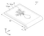
도 1a는 본 발명의 일 실시예에 따른 표시 장치의 사시도이다.
도 1b는 본 발명의 일 실시예에 따른 표시 장치의 단면도이다.
도 2a는 본 발명의 일 실시예에 따른 표시 장치의 사시도이다.
도 2b는 본 발명의 일 실시예에 따른 표시 장치의 단면도이다.
도 3a 및 도 3b는 본 발명의 일 실시예에 따른 표시 장치의 사시도이다.
도 4a는 본 발명의 일 실시예에 따른 유기발광 표시패널의 평면도이다.
도 4b는 본 발명의 일 실시예에 따른 표시 모듈의 단면도이다.
도 5a는 본 발명의 일 실시예에 따른 화소의 등가회로도이다.
도 5b는 본 발명의 일 실시예에 따른 유기발광 표시패널의 부분 단면도이다.
도 5c는 본 발명의 일 실시예에 따른 유기발광 표시패널의 부분 단면도이다.
도 6a 내지 도 6c는 본 발명의 일 실시예에 따른 박막 봉지층들의 단면도들이다.
도 7a는 본 발명의 일 실시예에 따른 터치센서층의 단면도이다.
도 7b 내지 7e는 본 발명의 일 실시예에 따른 터치센서층의 평면도들이다.
도 7f은 도 7e의 BB영역의 부분 확대도이다.
도 8a 내지 도 8d는 도 4b의 AA 영역의 부분 확대도이다.
도 9a 내지 도 9i는 도 8c에 도시된 표시 모듈의 제조 방법을 순차적으로 나타낸 단면도들이다.1A is a perspective view of a display device according to an embodiment of the present invention.
1B is a cross-sectional view of a display device according to an embodiment of the present invention.
2A is a perspective view of a display device according to an embodiment of the present invention.
2B is a cross-sectional view of a display device according to an embodiment of the present invention.
3A and 3B are perspective views of a display device according to an embodiment of the present invention.
4A is a plan view of an organic light emitting display panel according to an embodiment of the present invention.
4B is a cross-sectional view of a display module according to an embodiment of the present invention.
5A is an equivalent circuit diagram of a pixel according to an embodiment of the present invention.
5B is a partial cross-sectional view of an OLED display panel according to an embodiment of the present invention.
5C is a partial cross-sectional view of an OLED display panel according to an embodiment of the present invention.
6A-6C are cross-sectional views of thin-film encapsulation layers according to an embodiment of the present invention.
7A is a cross-sectional view of a touch sensor layer according to an embodiment of the present invention.
7B to 7E are top views of a touch sensor layer according to an embodiment of the present invention.
Fig. 7F is a partially enlarged view of the BB area of Fig. 7E.
Figs. 8A to 8D are partial enlarged views of the AA area in Fig. 4B. Fig.
9A to 9I are sectional views sequentially showing the manufacturing method of the display module shown in Fig. 8C.
이하, 도면을 참조하여 본 발명의 실시예들을 설명한다. 본 명세서에서, 어떤 구성요소(또는 영역, 층, 부분 등)가 다른 구성요소 "상에 있다", "연결 된다", 또는 "결합 된다"고 언급되는 경우에 그것은 다른 구성요소 상에 직접 연결/결합될 수 있거나 또는 그들 사이에 제3의 구성요소가 배치될 수도 있다는 것을 의미한다.Hereinafter, embodiments of the present invention will be described with reference to the drawings. In the present specification, when it is mentioned that any element (or region, layer, portion, etc.) is "on", "connected", or "coupled" to another element, Or a third component may be disposed therebetween.
동일한 도면부호는 동일한 구성요소를 지칭한다. 또한, 도면들에 있어서, 구성요소들의 두께, 비율, 및 치수는 기술적 내용의 효과적인 설명을 위해 과장된 것이다. "및/또는"은 연관된 구성들이 정의할 수 있는 하나 이상의 조합을 모두 포함한다.Like reference numerals refer to like elements. Also, in the drawings, thickness, ratio, and dimensions of components are exaggerated for an effective description of the technical content. "And / or" include all combinations of one or more of which the associated configurations can define.
제1, 제2 등의 용어는 다양한 구성요소들을 설명하는데 사용될 수 있지만, 상기 구성요소들은 상기 용어들에 의해 한정되어서는 안 된다. 상기 용어들은 하나의 구성요소를 다른 구성요소로부터 구별하는 목적으로만 사용된다. 예를 들어, 본 발명의 권리 범위를 벗어나지 않으면서 제1 구성요소는 제2 구성요소로 명명될 수 있고, 유사하게 제2 구성요소도 제1 구성요소로 명명될 수 있다. 단수의 표현은 문맥상 명백하게 다르게 뜻하지 않는 한, 복수의 표현을 포함한다.The terms first, second, etc. may be used to describe various components, but the components should not be limited by the terms. The terms are used only for the purpose of distinguishing one component from another. For example, without departing from the scope of the present invention, the first component may be referred to as a second component, and similarly, the second component may also be referred to as a first component. The singular expressions include plural expressions unless the context clearly dictates otherwise.
또한, "아래에", "하측에", "위에", "상측에" 등의 용어는 도면에 도시된 구성들의 연관관계를 설명하기 위해 사용된다. 상기 용어들은 상대적인 개념으로, 도면에 표시된 방향을 기준으로 설명된다.Also, terms such as "below "," below ", "above "," above ", and the like are used to describe the relationship of the configurations shown in the drawings. The terms are described relative to the direction shown in the figure in a relative concept.
"포함하다" 또는 "가지다" 등의 용어는 명세서 상에 기재된 특징, 숫자, 단계, 동작, 구성요소, 부품 또는 이들을 조합한 것이 존재함을 지정하려는 것이지, 하나 또는 그 이상의 다른 특징들이나 숫자, 단계, 동작, 구성요소, 부분품 또는 이들을 조합한 것들의 존재 또는 부가 가능성을 미리 배제하지 않는 것으로 이해되어야 한다.It will be understood that terms such as "comprise" or "comprise ", when used in this specification, specify the presence of stated features, integers, , &Quot; an ", " an ", " an "
이하에서는 본 발명의 일 실시예에 따른 표시 장치에 대해서 설명한다.Hereinafter, a display device according to an embodiment of the present invention will be described.
도 1a는 본 발명의 일 실시예에 따른 표시 장치의 사시도이다.1A is a perspective view of a display device according to an embodiment of the present invention.
도 1a에 도시된 것과 같이, 표시 장치(DD)의 표시면(IS)은 복수 개의 영역들을 포함할 수 있다. 표시 장치(DD)는 이미지(IM)가 표시되는 표시영역(DD-DA) 및 표시영역(DD-DA)에 인접한 비표시영역(DD-NDA)을 포함한다. 비표시영역(DD-NDA)은 이미지가 표시되지 않는 영역이다. 도 1a에는 이미지(IM)의 일 예로 화병을 도시하였다. 일 예로써, 표시영역(DD-DA)은 사각형상일 수 있다. 비표시영역(DD-NDA)은 표시영역(DD-DA)을 에워싸을 수 있다. 비표시영역(DD-NDA)은 다양한 형상을 가질 수 있으며, 어느 하나의 실시예로 한정되지 않는다.As shown in FIG. 1A, the display surface IS of the display device DD may include a plurality of areas. The display device DD includes a display area DD-DA in which the image IM is displayed and a non-display area DD-NDA adjacent to the display area DD-DA. The non-display area (DD-NDA) is an area where no image is displayed. In Fig. 1A, a vase is shown as an example of the image IM. As an example, the display area DD-DA may be rectangular. The non-display area DD-NDA can surround the display area DD-DA. The non-display area DD-NDA may have various shapes and is not limited to any one embodiment.
표시 장치(DD)는 일 부분이 벤딩된 형상을 가질 수 있다. 예를 들어, 도 1a에 도시된 것과 같이, 표시 장치(DD)는 벤딩된 형상을 가진 벤딩영역(BA) 및 플랫한 형상을 가진 비벤딩영역(NBA)으로 구분될 수 있다. 벤딩영역(BA)은 비벤딩영역(NBA)의 적어도 일 측에 인접할 수 있다. 한편, 이는 예시적으로 도시한 것이고, 본 발명의 일 실시예에 따른 표시 장치에 있어서, 벤딩영역 또는 비벤딩영역은 생략될 수도 있다.The display device DD may have a shape in which one portion is bent. For example, as shown in FIG. 1A, the display device DD can be divided into a bending area BA having a bent shape and a non-bending area NBA having a flat shape. The bending area BA may be adjacent to at least one side of the non-bending area NBA. On the other hand, this is illustrated by way of example, and in the display device according to the embodiment of the present invention, the bending region or the non-bending region may be omitted.
비벤딩영역(NBA)은 제1 방향(DR1)과 제2 방향(DR2)이 정의하는 면과 평행한다. 비벤딩영역(NBA)의 법선 방향은 제3 방향(DR3)이 지시한다. 제3 방향(DR3)은 각 부재들의 전면과 배면을 구분하는 기준축이다. 비벤딩영역(NBA)으로부터 벤딩된 벤딩영역(BA)은 제1 방향(DR1), 제2 방향(DR2), 및 제3 방향(DR3)과 교차하는 제4 방향(DR4)으로 이미지(IM)를 표시할 수 있다. 그러나, 제1 내지 제4 방향들(DR1 내지 DR4)이 지시하는 방향은 상대적인 개념으로서 다른 방향으로 변환될 수 있다.The nonbending region NBA is parallel to the plane defined by the first direction DR1 and the second direction DR2. The normal direction of the non-bending area NBA is indicated by the third direction DR3. The third direction DR3 is a reference axis for distinguishing the front surface and the back surface of the respective members. The bending area BA bending from the non-bending area NBA is the image IM in the fourth direction DR4 intersecting with the first direction DR1, the second direction DR2, and the third direction DR3. Can be displayed. However, the directions indicated by the first to fourth directions DR1 to DR4 can be converted into different directions as relative concepts.
도 1b는 도 1a에 도시된 표시 장치의 단면도이다. 도 1b는 제1 방향(DR1)과 제3 방향(DR3)이 정의하는 단면을 도시하였다.1B is a cross-sectional view of the display device shown in FIG. 1A. 1B shows a cross section defined by a first direction DR1 and a third direction DR3.
도 1b에 도시된 것과 같이, 표시 장치(DD)는 보호필름(PM), 표시 모듈(DM), 광학부재(LM), 윈도우(WM), 제1 접착부재(AM1), 제2 접착부재(AM2), 및 제3 접착부재(AM3)를 포함할 수 있다. 표시 모듈(DM)은 보호필름(PM)과 광학부재(LM) 사이에 배치된다. 광학부재(LM)는 표시 모듈(DM)과 윈도우(WM) 사이에 배치된다. 제1 접착부재(AM1)는 표시 모듈(DM)과 보호필름(PM)을 결합하고, 제2 접착부재(AM2)는 표시 모듈(DM)과 광학부재(LM)를 결합하고, 제3 접착부재(AM3)는 광학부재(LM)와 윈도우(WM)를 결합한다.1B, the display device DD includes a protective film PM, a display module DM, an optical member LM, a window WM, a first adhesive member AM1, a second adhesive member AM2, and a third adhesive member AM3. The display module DM is disposed between the protective film PM and the optical member LM. The optical member LM is disposed between the display module DM and the window WM. The first adhesive member AM1 combines the display module DM with the protective film PM while the second adhesive member AM2 combines the display module DM and the optical member LM, (AM3) combines the optical member (LM) and the window (WM).
보호필름(PM)은 표시 모듈(DM)을 보호한다. 보호필름(PM)은 외부에 노출된 제1 외면(OS-L)을 제공하고, 제1 접착부재(AM1)에 접착되는 접착면을 제공한다. 보호필름(PM)은 외부의 습기가 표시 모듈(DM)에 침투하는 것을 방지하고, 외부 충격을 흡수한다.The protective film PM protects the display module DM. The protective film PM provides a first outer surface OS-L exposed to the outside, and provides an adhesive surface to be bonded to the first adhesive member AM1. The protective film (PM) prevents external moisture from penetrating into the display module (DM) and absorbs external impact.
보호필름(PM)은 플라스틱 필름을 베이스층으로써 포함할 수 있다. 보호필름(PM)는 폴리에테르술폰(PES, polyethersulfone), 폴리아크릴레이트(PAR, polyacrylate), 폴리에테르 이미드(PEI,polyetherimide), 폴리에틸렌 나프탈레이트(PEN, polyethyelenen naphthalate), 폴리에틸렌 테레프탈레이트(PET, polyethyeleneterephthalate), 폴리페닐렌설파이드(PPS, polyphenylene sulfide), 폴리아릴레이트(polyarylate), 폴리이미드(PI, polyimide), 폴리카보네이트(PC, polycarbonate), 폴리아릴렌에테르술폰(poly(arylene ethersulfone)) 및 이들의 조합으로 이루어진 그룹에서 선택된 어느 하나를 포함하는 플라스틱 필름을 포함할 수 있다.The protective film (PM) may include a plastic film as a base layer. The protective film (PM) may be formed of a material selected from the group consisting of polyethersulfone (PES), polyacrylate (PAR), polyetherimide (PEI), polyethyelenenaphthalate (PEN), polyethylene terephthalate (PET) polyethyelenetherephthalate, polyphenylene sulfide (PPS), polyarylate, polyimide (PI), polycarbonate (PC), polyarylene ether sulfone and poly And a plastic film containing any one selected from the group consisting of combinations thereof.
보호필름(PM)을 구성하는 물질은 플라스틱 수지들에 제한되지 않고, 유/무기 복합재료를 포함할 수 있다. 보호필름(PM)은 다공성 유기층 및 유기층의 기공들에 충전된 무기물을 포함할 수 있다. 보호필름(PM)은 플라스틱 필름에 형성된 기능층을 더 포함할 수 있다. 상기 기능층은 수지층을 포함할 수 있다. 상기 기능층은 코팅 방식에 의해 형성될 수 있다. 본 발명의 일 실시예에서 보호필름(PM)은 생략될 수 있다.The material constituting the protective film (PM) is not limited to plastic resins, and may include an organic / inorganic composite material. The protective film PM may comprise a porous organic layer and an inorganic material filled in the pores of the organic layer. The protective film PM may further comprise a functional layer formed on the plastic film. The functional layer may include a resin layer. The functional layer may be formed by a coating method. In one embodiment of the present invention, the protective film PM may be omitted.
윈도우(WM)는 외부 충격으로부터 표시 모듈(DM)를 보호하고, 사용자에게 입력면을 제공할 수 있다. 윈도우(WM)은 외부에 노출된 제2 외면(OS-U)을 제공하고, 제2 접착부재(AM2)에 접착되는 접착면을 제공한다. 도 1a 및 도 1b에 도시된 표시면(IS)이 제2 외면(OS-U)일 수 있다.The window WM protects the display module DM from an external impact and can provide an input surface to the user. The window WM provides a second outer surface OS-U exposed to the outside and provides an adhesive surface to be adhered to the second adhesive member AM2. The display surface IS shown in Figs. 1A and 1B may be a second outer surface OS-U.
윈도우(WM)는 플라스틱 필름을 포함할 수 있다. 윈도우(WM)는 다층구조를 가질 수 있다. 윈도우(WM)는 유리 기판, 플라스틱 필름, 플라스틱 기판으로부터 선택된 다층구조를 가질 수 있다. 윈도우(WM)는 베젤패턴을 더 포함할 수 있다. 상기 다층구조는 연속공정 또는 접착층을 이용한 접착공정을 통해 형성될 수 있다.The window (WM) may comprise a plastic film. The window (WM) can have a multi-layer structure. The window (WM) may have a multilayer structure selected from a glass substrate, a plastic film, and a plastic substrate. The window (WM) may further include a bezel pattern. The multi-layer structure may be formed through a continuous process or an adhesion process using an adhesive layer.
광학부재(LM)는 외부광 반사율을 감소시킨다. 광학부재(LM)는 적어도 편광필름을 포함할 수 있다. 광학부재(LM)는 위상차 필름을 더 포함할 수 있다. 본 발명의 일 실시예에서 광학부재(LM)는 생략될 수 있다.The optical member LM reduces the external light reflectance. The optical member LM may include at least a polarizing film. The optical member (LM) may further include a retardation film. In an embodiment of the present invention, the optical member LM may be omitted.
표시 모듈(DM)은 유기발광 표시패널(DP) 및 터치센서층(TS)을 포함할 수 있다. 터치센서층(TS)은 유기발광 표시패널(DP) 상에 직접 배치된다. 본 명세서에서 "직접 배치된다"는 것은 별도의 접착층을 이용하여 부착하는 것을 제외하며, 연속공정에 의해 형성된 것을 의미한다.The display module DM may include an organic light emitting display panel DP and a touch sensor layer TS. The touch sensor layer TS is disposed directly on the organic light emitting display panel DP. As used herein, the term " directly disposed " means that it is formed by a continuous process except that it is adhered using a separate adhesive layer.
유기발광 표시패널(DP)은 입력된 영상 데이터에 대응하는 이미지(IM, 도 1a 참조)를 생성한다. 유기발광 표시패널(DP)은 두께 방향(DR3)에서 마주하는 제1 표시패널면(BS1-L) 및 제2 표시패널면(BS1-U)을 제공한다. 본 실시예에서 유기발광 표시패널(DP)을 예시적으로 설명하였으나, 표시패널은 이에 제한되지 않는다.The organic light emitting display panel DP generates an image IM (see Fig. 1A) corresponding to the input image data. The organic light emitting display panel DP provides a first display panel face BS1-L and a second display panel face BS1-U facing in the thickness direction DR3. Although the organic light emitting display panel DP has been exemplarily described in this embodiment, the display panel is not limited thereto.
터치센서층(TS)은 외부입력의 좌표정보를 획득한다. 터치센서층(TS)은 정전용량 방식으로 외부입력을 감지할 수 있다.The touch sensor layer TS acquires the coordinate information of the external input. The touch sensor layer (TS) can sense an external input by a capacitive method.
별도로 도시하지 않았으나, 본 발명의 일 실시예에 따른 표시 모듈(DM)은 반사방지층을 더 포함할 수도 있다. 반사방지층은 컬러필터 또는 도전층/절연층/도전층의 적층 구조물을 포함할 수 있다. 반사방지층은 외부로부터 입사된 광을 흡수 또는 상쇄간섭 또는 편광시켜 외부광 반사율을 감소시킬 수 있다. 반사방지층은 광학부재(LM)의 기능을 대체할 수 있다.Although not shown separately, the display module DM according to an embodiment of the present invention may further include an anti-reflection layer. The antireflection layer may include a color filter or a laminated structure of a conductive layer / insulating layer / conductive layer. The antireflection layer can reduce the external light reflectance by absorbing or destructively interfering or polarizing light incident from the outside. The antireflection layer can replace the function of the optical member LM.
제1 접착부재(AM1), 제2 접착부재(AM2), 및 제3 접착부재(AM3) 각각은 광학투명접착필름(OCA, Optically Clear Adhesive film) 또는 광학투명접착수지(OCR, Optically Clear Resin) 또는 감압접착필름(PSA, Pressure Sensitive Adhesive film)과 같은 유기 접착층일 수 있다. 유기 접착층은 폴리우레탄계, 폴리아크릴계, 폴리에스테르계, 폴리에폭시계, 폴리초산비닐계 등의 접착물질을 포함할 수 있다.Each of the first adhesive member AM1, the second adhesive member AM2 and the third adhesive member AM3 is made of an optically clear adhesive film (OCA) or an optically clear resin (OCR) Or an organic adhesive layer such as a pressure sensitive adhesive film (PSA). The organic adhesive layer may include an adhesive material such as polyurethane, polyacrylic, polyester, polyepoxy, polyvinyl acetate, and the like.
별도로 도시하지 않았으나, 표시 장치(DD)는 도 1a 및 도 1B에 도시된 상태를 유지하기 위해 상기 기능층들을 지지하는 프레임 구조물을 더 포함할 수 있다. 프레임 구조물은 관절 구조 또는 힌지 구조를 포함할 수 있다.Although not shown separately, the display device DD may further include a frame structure for supporting the functional layers to maintain the state shown in Figs. 1A and 1B. The frame structure may include a joint structure or a hinge structure.
표시 장치(DD)의 벤딩영역(BA)은 일정한 곡률반경으로 벤딩된 형상을 가질 수 있다. 또는, 벤딩영역(BA)은 비벤딩영역(NBA)으로부터 거리가 멀어질수록 곡률반경이 감소하도록 벤딩된 형상을 가질 수 있다. 다만 이에 한정되지 않고, 벤딩영역(BA)는 다양한 곡률반경으로 벤딩될 수 있다.The bending area BA of the display device DD may have a shape bent with a constant radius of curvature. Alternatively, the bending area BA may have a bended shape such that the radius of curvature decreases as the distance from the non-bending area NBA increases. However, the present invention is not limited to this, and the bending area BA can be bent at various curvature radii.
한편, 본 발명의 일 실시예에 따른 표시 장치에 있어서, 보호 필름(PM), 접착층들(AM1, AM2, AM3), 광학부재(LM) 및 윈도우(WM) 중 적어도 어느 하나는 생략될 수 있다. 본 발명의 일 실시예에 따른 표시 장치는 다양한 부재들의 조합을 포함할 수 있으며, 어느 하나의 실시예로 한정되지 않는다.At least one of the protective film PM, the adhesive layers AM1, AM2, and AM3, the optical member LM, and the window WM may be omitted in the display device according to an exemplary embodiment of the present invention . The display device according to an embodiment of the present invention may include a combination of various members and is not limited to any one embodiment.
도 2a는 본 발명의 일 실시예에 따른 표시 장치의 사시도이다. 도 2b는 본 발명의 일 실시예에 따른 표시 장치의 단면도이다. 이하, 도 2a 및 도 2b를 참조하여 표시 장치(DD-1)에 대해 설명한다. 한편, 도 1a 및 도 1b에서 설명한 구성과 동일 구성은 동일한 참조 부호를 부여하고 설명은 생략한다.2A is a perspective view of a display device according to an embodiment of the present invention. 2B is a cross-sectional view of a display device according to an embodiment of the present invention. Hereinafter, the display device DD-1 will be described with reference to Figs. 2A and 2B. The same components as those described in Figs. 1A and 1B are denoted by the same reference numerals, and a description thereof will be omitted.
도 2a에 도시된 것과 같이, 표시 장치(DD-1)는 하나의 비벤딩영역(NBA)과 비벤딩영역(NBA)의 양 측면에 제1 벤딩영역(BA1) 및 제2 벤딩영역(BA2)을 포함할 수 있다. 도 2b는 제1 방향(DR1)과 제3 방향(DR3)이 정의하는 단면을 도시하였다.2A, the display device DD-1 has a first bending area BA1 and a second bending area BA2 on both sides of one non-bending area NBA and the non-bending area NBA, . ≪ / RTI > FIG. 2B shows a cross section defined by the first direction DR1 and the third direction DR3.
표시 장치(DD-1)는 제1 벤딩영역(BA1) 및 제2 벤딩영역(BA2)을 포함할 수 있다. 벤딩 영역(BA1, BA2)들은 비벤딩영역(NBA)을 사이에 두고 서로 이격되도록 정의될 수 있다. 제1 벤딩영역(BA1)은 비벤딩영역(NBA)의 일측에 인접하여 제4 방향(DR4)으로 볼록하도록 벤딩된 형상을 갖는다. 제2 벤딩영역(BA2)은 비벤딩영역(NBA)의 타측에 인접하여 제5 방향(DR5)으로 볼록하도록 벤딩된 형상을 갖는다.The display device DD-1 may include a first bending area BA1 and a second bending area BA2. The bending areas BA1 and BA2 may be defined to be spaced apart from each other with the non-bending area NBA therebetween. The first bending area BA1 has a shape bending convexly in the fourth direction DR4 adjacent to one side of the non-bending area NBA. The second bending area BA2 has a shape bending convexly in the fifth direction DR5 adjacent to the other side of the non-bending area NBA.
표시 장치(DD-1)는 제3 방향(DR3)을 향해 대체로 볼록한 형상을 가질 수 있다. 한편, 이는 예시적으로 도시한 것이고, 표시 장치(DD-1)는 제1 벤딩영역(BA1) 및 제2 벤딩영역(BA2) 각각의 형상에 따라 상측으로 오목한 형상을 가질 수도 있다. 본 발명의 일 실시예에 따른 표시 장치(DD-1)는 다양한 형상을 가질 수 있으며, 어느 하나의 실시예로 한정되지 않는다.The display device DD-1 may have a generally convex shape toward the third direction DR3. The display device DD-1 may have a concave shape upward depending on the shapes of the first bending area BA1 and the second bending area BA2, respectively. The display device DD-1 according to an embodiment of the present invention may have various shapes and is not limited to any one embodiment.
도 1a 내지 도 2b는 표시 장치(DD, DD-1)의 일례로 벤디드 표시 장치를 도시하였다. 그러나, 본 발명은 플렉서블한 폴더블 표시 장치 또는 말려지는 롤러블 표시 장치일 수 있고, 특별히 제한되지 않는다. 또한, 본 실시예에서 플렉서블 표시 장치를 도시하였으나, 본 발명은 이에 제한되지 않는다. 본 실시예에 따른 표시 장치(DD)는 플랫한 리지드 표시 장치일 수도 있고, 휘어진 리지드 표시 장치일 수도 있다. 본 발명에 따른 표시 장치(DD)는 텔레비전, 모니터 등과 같은 대형 전자장치를 비롯하여, 휴대 전화, 태블릿, 자동차 네비게이션, 게임기, 스마트 와치 등과 같은 중소형 전자장치 등에 사용될 수 있다.1A and 2B show a bent display device as an example of the display devices DD and DD-1. However, the present invention can be a flexible, foldable display device or a rolled-up display device, and is not particularly limited. Although the flexible display device is shown in this embodiment, the present invention is not limited thereto. The display device DD according to the present embodiment may be a flat rigid display device or a warped rigid display device. The display device DD according to the present invention can be used for a large-sized electronic device such as a television, a monitor, etc., and a small-sized electronic device such as a mobile phone, a tablet, a car navigation system, a game machine,
도 3a 및 도 3b는 본 발명의 일 실시예에 따른 표시 장치의 사시도이다. 도 3a는 펼쳐진 상태의 표시 장치(DD-2)를 도시하였고, 도 3b는 벤딩된 상태의 표시 장치(DD-2)를 도시하였다.3A and 3B are perspective views of a display device according to an embodiment of the present invention. Fig. 3A shows a display device DD-2 in an unfolded state, and Fig. 3B shows a display device DD-2 in a bending state.
표시 장치(DD-2)는 하나의 벤딩영역(BA)과 하나의 비벤딩영역(NBA)을 포함할 수 있다. 표시 장치(DD-2)의 비표시영역(DD-NDA)이 벤딩될 수 있다. 다만, 본 발명의 일 실시예에서 표시 장치(DD-2)의 벤딩영역은 변경될 수 있다.The display device DD-2 may include one bending area BA and one non-bending area NBA. The non-display area DD-NDA of the display device DD-2 can be bent. However, the bending area of the display device DD-2 may be changed in an embodiment of the present invention.
본 실시예에 따른 표시 장치(DD-2)는, 하나의 형태로 고정되어 작동할 수 있다. 표시 장치(DD-2)는 도 3b에 도시된 것과 같이 벤딩된 상태로 작동할 수 있다. 표시 장치(DD-2)는 벤딩된 상태로 프레임 등에 고정되고, 프레임이 전자장치의 하우징과 결합될 수 있다.The display device DD-2 according to the present embodiment can be fixedly operated in one form. The display device DD-2 can operate in a bent state as shown in Fig. 3B. The display device DD-2 is fixed to a frame or the like in a bent state, and the frame can be engaged with the housing of the electronic device.
본 실시예에 따른 표시 장치(DD-2)는 도 1b에 도시된 것과 동일한 단면 구조를 가질 수 있다. 한편, 이는 예시적으로 도시된 것이고, 비벤딩영역(NBA)과 벤딩영역(BA)은 다른 적층 구조를 가질 수도 있다. 예를 들어, 비벤딩영역(NBA)은 도 1b에 도시된 것과 동일한 단면 구조를 갖고, 벤딩영역(BA)은 도 1b에 도시된 것과 다른 단면 구조를 가질 수 있다. 벤딩영역(BA)에는 광학부재(LM) 및 윈도우(WM)가 미배치될 수 있다. 즉, 광학부재(LM) 및 윈도우(WM)는 비벤딩영역(NBA)에만 배치될 수 있다. 제2 접착부재(AM2) 및 제3 접착부재(AM3) 역시 벤딩영역(BA)에 미배치될 수 있다. 도 1b에 도시된 구성들 중 적어도 어느 하나의 구성이 비벤딩영역(NBA)에만 중첩하고 벤딩영역(BA)에는 비중첩하도록 제공됨에 따라, 벤딩영역(BA)은 비벤딩영역(NBA)에 비해 상대적으로 슬림한 두께를 가질 수 있다. 이에 따라, 벤딩영역(BA)이 용이하게 벤딩될 수 있다.The display device DD-2 according to this embodiment may have the same cross-sectional structure as that shown in Fig. 1B. On the other hand, this is illustrated by way of example, and the non-bending region NBA and the bending region BA may have different lamination structures. For example, the non-bending region NBA has the same cross-sectional structure as that shown in Fig. 1B, and the bending region BA may have a cross-sectional structure different from that shown in Fig. 1B. The optical member LM and the window WM may not be disposed in the bending area BA. That is, the optical member LM and the window WM can be disposed only in the non-bending area NBA. The second adhesive member AM2 and the third adhesive member AM3 may not be disposed in the bending area BA. 1B is provided so as to overlap only the non-bending region NBA and to be non-overlapping in the bending region BA, the bending region BA is formed to be larger than the non-bending region NBA It can have a relatively slim thickness. Thus, the bending area BA can be bent easily.
도 4a는 본 발명의 일 실시예에 따른 유기발광 표시패널의 평면도이다. 도 4b는 본 발명의 일 실시예에 따른 표시 모듈의 단면도이다.4A is a plan view of an organic light emitting display panel according to an embodiment of the present invention. 4B is a cross-sectional view of a display module according to an embodiment of the present invention.
도 4a에 도시된 것과 같이, 유기발광 표시패널(DP)은 평면상에서 표시영역(DA)과 비표시영역(NDA)을 포함한다. 유기발광 표시패널(DP)의 표시영역(DA) 및 비표시영역(NDA)은 표시 장치(DD, 도 1a 참조)의 표시영역(DD-DA, 도 1a 참조) 및 비표시영역(DD-NDA, 도 1a 참조)에 각각 대응한다. 유기발광 표시패널(DP)의 표시영역(DA) 및 비표시영역(NDA)은 표시 장치(DD, 도 1a 참조)의 표시영역(DD-DA, 도 1a 참조) 및 비표시영역(DD-NDA, 도 1a 참조)과 반드시 동일할 필요는 없고, 유기발광 표시패널(DP)의 구조/디자인에 따라 변경될 수 있다.As shown in Fig. 4A, the organic light emitting display panel DP includes a display area DA and a non-display area NDA on a plane. The display area DA and the non-display area NDA of the organic light emitting display panel DP are arranged in the display area DD-DA (see Fig. 1A) and the non-display area DD-NDA , See Fig. 1A), respectively. The display area DA and the non-display area NDA of the organic light emitting display panel DP are arranged in the display area DD-DA (see Fig. 1A) and the non-display area DD-NDA (See Fig. 1A), and may be changed according to the structure / design of the organic light emitting display panel DP.
유기발광 표시패널(DP)은 복수 개의 화소들(PX)을 포함한다. 복수 개의 화소들(PX)이 배치된 영역이 표시영역(DA)으로 정의된다. 본 실시예에서 비표시영역(NDA)은 표시영역(DA)의 테두리를 따라 정의될 수 있다.The organic light emitting display panel DP includes a plurality of pixels PX. An area in which a plurality of pixels PX are arranged is defined as a display area DA. In the present embodiment, the non-display area NDA can be defined along the rim of the display area DA.
유기발광 표시패널(DP)은 게이트 라인들(GL), 데이터 라인들(DL), 발광 라인들(EL), 제어신호 라인(SL-D), 초기화 전압 라인(SL-Vint), 전압 라인(SL-VDD), 전원 공급 라인(E-VSS), 및 패드부(PD)를 포함한다.The organic light emitting display panel DP includes gate lines GL, data lines DL, light emitting lines EL, control signal lines SL-D, initializing voltage lines SL-Vint, SL-VDD, a power supply line (E-VSS), and a pad portion PD.
게이트 라인들(GL)은 복수 개의 화소들(PX) 중 대응하는 화소(PX)에 각각 연결되고, 데이터 라인들(DL)은 복수 개의 화소들(PX) 중 대응하는 화소(PX)에 각각 연결된다. 발광 라인들(EL) 각각은 게이트 라인들(GL) 중 대응하는 게이트 라인에 나란하게 배열될 수 있다. 제어신호 라인(SL-D)은 게이트 구동회로(GDC)에 제어신호들을 제공할 수 있다. 초기화 전압 라인(SL-Vint)은 복수 개의 화소들(PX)에 초기화 전압을 제공할 수 있다. 전압 라인(SL-VDD)은 복수 개의 화소들(PX)에 연결되며, 복수 개의 화소들(PX)에 제1 전압을 제공할 수 있다. 전압 라인(SL-VDD)은 제1 방향(DR1)으로 연장하는 복수의 라인들 및 제2 방향(DR2)으로 연장하는 복수의 라인들을 포함할 수 있다. 전원 공급 라인(E-VSS)은 비표시영역(NDA)에는 표시영역(DA)의 3개의 측면을 둘러싸며 배치될 수 있다. 전원 공급 라인(E-VSS)의 복수 개의 화소들(PX)에 공통 전압(예컨대, 제2 전압)을 제공할 수 있다. 공통 전압은 상기 제1 전압보다 낮은 레벨의 전압일 수 있다.The gate lines GL are connected to the corresponding pixels PX of the plurality of pixels PX and the data lines DL are connected to the corresponding pixels PX of the plurality of pixels PX, do. Each of the light emitting lines EL may be arranged in parallel to a corresponding one of the gate lines GL. The control signal line SL-D may provide control signals to the gate drive circuit GDC. The initialization voltage line SL-Vint may provide an initialization voltage to the plurality of pixels PX. The voltage line SL-VDD is connected to the plurality of pixels PX and can provide the first voltage to the plurality of pixels PX. The voltage line SL-VDD may include a plurality of lines extending in the first direction DR1 and a plurality of lines extending in the second direction DR2. The power supply line E-VSS may be disposed around the three side surfaces of the display area DA in the non-display area NDA. (E.g., a second voltage) to the plurality of pixels PX of the power supply line E-VSS. The common voltage may be a voltage lower than the first voltage.
비표시영역(NDA)의 일측에는 게이트 라인들(GL) 및 발광 라인들(EL)이 연결된 게이트 구동회로(GDC)가 배치될 수 있다. 게이트 라인들(GL), 데이터 라인들(DL), 발광 라인들(EL), 제어신호 라인(SL-D), 초기화 전압 라인(SL-Vint), 전압 라인(SL-VDD) 및 전원 공급 라인(E-VSS) 중 일부는 동일한 층에 배치되고, 일부는 다른 층에 배치된다.A gate driving circuit GDC connected to the gate lines GL and the light emitting lines EL may be disposed at one side of the non-display area NDA. The gate lines GL, the data lines DL, the light emission lines EL, the control signal lines SL-D, the initialization voltage lines SL-Vint, the voltage lines SL- (E-VSS) are arranged in the same layer, and some are arranged in different layers.
패드부(PD)는 데이터 라인들(DL), 제어신호 라인(SL-D), 초기화 전압 라인(SL-Vint), 및 전압 라인(SL-VDD)의 말단에 연결될 수 있다.The pad portion PD may be connected to the ends of the data lines DL, the control signal line SL-D, the initialization voltage line SL-Vint, and the voltage line SL-VDD.
도 4b에 도시된 것과 같이, 유기발광 표시패널(DP)은 베이스층(SUB), 베이스층(SUB) 상에 배치된 회로층(DP-CL), 표시층(DP-OLED), 및 박막 봉지층(TFE)을 포함한다.4B, the organic light emitting display panel DP includes a base layer SUB, a circuit layer DP-CL disposed on the base layer SUB, a display layer DP-OLED, Layer (TFE).
베이스층(SUB)은 적어도 하나의 플라스틱 필름을 포함할 수 있다. 베이스층(SUB)은 플렉서블한 기판으로 플라스틱 기판, 유리 기판, 메탈 기판, 또는 유/무기 복합재료 기판 등을 포함할 수 있다. 플라스틱 기판은 아크릴계 수지, 메타크릴계 수지, 폴리이소프렌, 비닐계 수지, 에폭시계 수지, 우레탄계 수지, 셀룰로오스계 수지, 실록산계 수지, 폴리이미드계 수지, 폴리아미드계 수지 및 페릴렌계 수지 중 적어도 어느 하나를 포함할 수 있다.The base layer (SUB) may comprise at least one plastic film. The base layer (SUB) is a flexible substrate, and may include a plastic substrate, a glass substrate, a metal substrate, or an organic / inorganic composite material substrate. The plastic substrate may be at least one of an acrylic resin, a methacrylic resin, a polyisoprene, a vinyl resin, an epoxy resin, a urethane resin, a cellulose resin, a siloxane resin, a polyimide resin, a polyamide resin, . ≪ / RTI >
회로층(DP-CL)은 복수 개의 절연층들, 복수 개의 도전층들 및 반도체층을 포함할 수 있다. 회로층(DP-CL)의 복수 개의 도전층들은 신호라인들 또는 화소의 제어회로를 구성할 수 있다.The circuit layer DP-CL may include a plurality of insulating layers, a plurality of conductive layers, and a semiconductor layer. The plurality of conductive layers of the circuit layer DP-CL may constitute control circuits of signal lines or pixels.
표시층(DP-OLED)은 유기발광 다이오드들을 포함한다.The display layer (DP-OLED) includes organic light emitting diodes.
박막 봉지층(TFE)은 표시층(DP-OLED)을 밀봉한다. 박막 봉지층(TFE)은 무기층과 유기층을 포함한다. 박막 봉지층(TFE)은 적어도 2개의 무기층들과 그 사이에 배치된 유기층을 포함할 수 있다. 무기층들은 수분/산소로부터 표시층(DP-OLED)을 보호하고, 유기층은 먼지 입자와 같은 이물질로부터 표시층(DP-OLED)을 보호한다. 무기층은 실리콘 나이트라이드층, 실리콘 옥시 나이트라이드층 및 실리콘 옥사이드층 등을 포함할 수 있다. 유기층은 아크릴 계열 유기물질을 포함할 수 있고, 이에 제한되지 않는다.The thin film encapsulation layer (TFE) seals the display layer (DP-OLED). The thin film encapsulation layer (TFE) includes an inorganic layer and an organic layer. The thin film encapsulation layer (TFE) may comprise at least two inorganic layers and an organic layer disposed therebetween. The inorganic layers protect the display layer (DP-OLED) from water / oxygen, and the organic layer protects the display layer (DP-OLED) from foreign substances such as dust particles. The inorganic layer may include a silicon nitride layer, a silicon oxynitride layer, a silicon oxide layer, and the like. The organic layer may include, but is not limited to, acrylic based organic materials.
터치센서층(TS)은 박막 봉지층(TFE) 상에 직접 배치된다. 터치센서층(TS)은 터치센서들과 터치 신호라인들을 포함한다. 터치센서들과 터치 신호라인들은 단층 또는 다층구조를 가질 수 있다.The touch sensor layer TS is disposed directly on the thin-film encapsulation layer (TFE). The touch sensor layer TS includes touch sensors and touch signal lines. The touch sensors and the touch signal lines may have a single layer or a multi-layer structure.
터치센서들과 터치 신호라인들은 ITO(indium tin oxide), IZO(indium zinc oxide), ZnO(zinc oxide), ITZO(indium tin zinc oxide), PEDOT, 금속 나노 와이어, 그라핀을 포함할 수 있다. 터치센서들과 터치 신호라인들은 금속층, 예컨대 몰리브덴, 은, 티타늄, 구리, 알루미늄, 또는 이들의 합금을 포함할 수 있다. 터치센서들과 터치 신호라인들은 동일한 층구조를 갖거나, 다른 층구조를 가질 수 있다. 터치센서층(TS)에 대한 구체적인 내용은 후술한다.The touch sensors and the touch signal lines may include ITO (indium tin oxide), IZO (indium zinc oxide), ZnO (zinc oxide), ITZO (indium tin zinc oxide), PEDOT, metal nanowire, and graphene. The touch sensors and touch signal lines may comprise a metal layer, such as molybdenum, silver, titanium, copper, aluminum, or alloys thereof. The touch sensors and the touch signal lines may have the same layer structure or different layer structures. Details of the touch sensor layer TS will be described later.
도 5a는 본 발명의 일 실시예에 따른 화소의 등가회로도이다.5A is an equivalent circuit diagram of a pixel according to an embodiment of the present invention.
도 5a에는 복수 개의 데이터 라인들(DL, 도 4a 참조) 중 k번째 데이터 라인(DLk)에 연결된 i번째 화소(PXi)를 예시적으로 도시하였다.5A illustrates an i-th pixel PXi connected to a k-th data line DLk among a plurality of data lines DL (see FIG. 4A).
i번째 화소(PXi)는 유기발광 다이오드(OLED) 및 유기발광 다이오드를 제어하는 화소 구동회로를 포함한다. 구동회로는 7개의 박막 트랜지스터들(T1~T7) 및 하나의 스토리지 커패시터(Cst)를 포함할 수 있다. 구동 트랜지스터는 유기발광 다이오드(OLED)에 공급되는 구동전류를 제어한다. 제2 트랜지스터(T2)의 출력전극은 유기발광 다이오드(OLED)와 전기적으로 연결된다. 제2 트랜지스터(T2)의 출력전극은 유기발광 다이오드(OLED)의 애노드와 직접 접촉하거나, 다른 트랜지스터(본 실시예에서 제6 트랜지스터(T6))를 경유하여 연결될 수 있다.The i-th pixel PXi includes an organic light emitting diode (OLED) and a pixel driving circuit for controlling the organic light emitting diode. The driving circuit may include seven thin film transistors (T1 to T7) and one storage capacitor (Cst). The driving transistor controls the driving current supplied to the organic light emitting diode (OLED). The output electrode of the second transistor T2 is electrically connected to the organic light emitting diode OLED. The output electrode of the second transistor T2 may be in direct contact with the anode of the organic light emitting diode OLED or may be connected via another transistor (the sixth transistor T6 in this embodiment).
제어 트랜지스터의 제어 전극은 제어 신호를 수신할 수 있다. i번째 화소(PXi)에 인가되는 제어 신호는 i-1번째 게이트 신호(Si-1), i번째 게이트 신호(Si), i+1번째 게이트 신호(Si+1), 데이터 신호(Dk), 및 i번째 발광 제어 신호(Ei)를 포함할 수 있다. 본 발명의 실시예에서 제어 트랜지스터는 제1 트랜지스터(T1) 및 제3 내지 제7 트랜지스터들(T3~T7)을 포함할 수 있다.The control electrode of the control transistor can receive the control signal. The control signal applied to the i-th pixel PXi is an i-th gate signal Si-1, an i-th gate signal Si, an i + 1-th gate signal Si + 1, a data signal Dk, And an i < th > emission control signal Ei. In an embodiment of the present invention, the control transistor may include a first transistor T1 and third to seventh transistors T3 to T7.
제1 트랜지스터(T1)는 k번째 데이터 라인(DLk)에 접속된 입력전극, i번째 게이트 라인(GLi)에 접속된 제어 전극, 및 제2 트랜지스터(T2)의 출력전극에 접속된 출력전극을 포함한다. 제1 트랜지스터(T1)는 i번째 게이트 라인(GLi)에 인가된 게이트 신호(Si, 이하 i번째 게이트 신호)에 의해 턴-온되고, k번째 데이터 라인(DLk)에 인가된 데이터 신호(Dk)를 스토리지 커패시터(Cst)에 제공한다. The first transistor T1 includes an input electrode connected to the k-th data line DLk, a control electrode connected to the i-th gate line GLi, and an output electrode connected to the output electrode of the second transistor T2 do. The first transistor T1 is turned on by a gate signal Si applied to an i-th gate line GLi and is then turned on by a data signal Dk applied to the k-th data line DLk. To the storage capacitor Cst.
도 5b는 본 발명의 일 실시예에 따른 유기발광 표시패널의 부분 단면도이다. 도 5c는 본 발명의 일 실시예에 따른 유기발광 표시패널의 부분 단면도이다. 구체적으로, 도 5b는 도 5a에 도시된 등가회로의 제1 트랜지스터(T1)에 대응하는 부분의 단면을 도시하였다. 도 5c는 도 5a에 도시된 등가회로의 제2 트랜지스터(T2), 제6 트랜지스터(T6) 및 유기발광 다이오드(OLED)에 대응하는 부분의 단면을 도시하였다.5B is a partial cross-sectional view of an OLED display panel according to an embodiment of the present invention. 5C is a partial cross-sectional view of an OLED display panel according to an embodiment of the present invention. Specifically, FIG. 5B shows a cross section of a portion corresponding to the first transistor T1 of the equivalent circuit shown in FIG. 5A. 5C shows a cross section of a portion corresponding to the second transistor T2, the sixth transistor T6 and the organic light emitting diode OLED of the equivalent circuit shown in Fig. 5A.
도 5b 및 도 5c를 참조하면, 베이스층(SUB) 상에 버퍼층(BFL)이 배치될 수 있다. 버퍼층(BFL)은 베이스층(SUB)과 도전성 패턴들 또는 반도체 패턴들의 결합력을 향상시킨다. 버퍼층(BFL)은 무기층을 포함할 수 있다. 별도로 도시되지 않았으나, 이물질이 유입되는 것을 방지하는 배리어층이 베이스층(SUB)의 상면에 더 배치될 수도 있다. 버퍼층(BFL)과 배리어층은 선택적으로 배치/생략될 수 있다.Referring to FIGS. 5B and 5C, a buffer layer BFL may be disposed on the base layer SUB. The buffer layer BFL improves the bonding strength between the base layer SUB and the conductive patterns or semiconductor patterns. The buffer layer (BFL) may include an inorganic layer. Although not shown separately, a barrier layer for preventing foreign matter from entering may be further disposed on the upper surface of the base layer SUB. The buffer layer (BFL) and the barrier layer may be optionally disposed / omitted.
버퍼층(BFL) 상에 제1 트랜지스터(T1)의 반도체 패턴(OSP1: 이하 제1 반도체 패턴), 제2 트랜지스터(T2)의 반도체 패턴(OSP2: 이하 제2 반도체 패턴), 제6 트랜지스터(T6)의 반도체 패턴(OSP6: 이하 제6 반도체 패턴)이 배치된다. 제1 반도체 패턴(OSP1), 제2 반도체 패턴(OSP2), 및 제6 반도체 패턴(OSP6)은 아몰포스 실리콘, 폴리 실리콘, 금속 산화물 반도체에서 선택될 수 있다.The semiconductor pattern OSP1 (hereafter referred to as a first semiconductor pattern) of the first transistor T1, the semiconductor pattern OSP2 (hereinafter referred to as a second semiconductor pattern) of the second transistor T2, and the sixth transistor T6 on the buffer layer BFL, (OSP6: hereinafter referred to as a sixth semiconductor pattern) is disposed. The first semiconductor pattern OSP1, the second semiconductor pattern OSP2, and the sixth semiconductor pattern OSP6 may be selected from amorphous silicon, polysilicon, and metal oxide semiconductors.
제1 반도체 패턴(OSP1), 제2 반도체 패턴(OSP2) 및 제6 반도체 패턴(OSP6) 위에는 제1 절연층(10)이 배치될 수 있다. 도 5b 및 도 5c에서는 제1 절연층(10)이 제1 반도체 패턴(OSP1), 제2 반도체 패턴(OSP2) 및 제6 반도체 패턴(OSP6)을 커버하는 층 형태로 제공되는 것을 예시적으로 도시하였으나, 제1 절연층(10)은 제1 반도체 패턴(OSP1), 제2 반도체 패턴(OSP2) 및 제6 반도체 패턴(OSP6) 에 대응하여 배치된 패턴으로 제공될 수도 있다.The first insulating
제1 절연층(10)은 복수 개의 무기 박막들을 포함할 수 있다. 복수 개의 무기 박막들은 실리콘 나이트라이드층, 실리콘 옥시 나이트라이드층 및 실리콘 옥사이드층을 포함할 수 있다.The first insulating
제1 절연층(10) 상에는 제1 트랜지스터(T1)의 제어 전극(GE1: 이하, 제1 제어전극), 제2 트랜지스터(T2)의 제어 전극(GE2: 이하, 제2 제어전극), 제6 트랜지스터(T6)의 제어 전극(GE6: 이하, 제6 제어전극)이 배치된다. 제1 제어 전극(GE1), 제2 제어 전극(GE2), 제6 제어 전극(GE6)은 게이트 라인들(GL, 도 4a 참조)과 동일한 포토리소그래피 공정에 따라 제조될 수 있다.A control electrode GE1 (hereinafter referred to as a first control electrode) of the first transistor T1, a control electrode GE2 (hereinafter referred to as a second control electrode) of the second transistor T2, And a control electrode GE6 (hereinafter referred to as a sixth control electrode) of the transistor T6. The first control electrode GE1, the second control electrode GE2 and the sixth control electrode GE6 may be manufactured according to the same photolithography process as the gate lines GL (see Fig. 4A).
제1 절연층(10) 상에는 제1 제어 전극(GE1), 제2 제어 전극(GE2) 및 제6 제어 전극(GE6)을 커버하는 제2 절연층(20)이 배치될 수 있다. 제2 절연층(20)은 평탄한 상면을 제공할 수 있다. 제2 절연층(20)은 유기 물질 및/또는 무기 물질을 포함할 수 있다.The second insulating
제2 절연층(20) 상에 제1 트랜지스터(T1)의 입력전극(SE1: 이하, 제1 입력전극) 및 출력전극(DE1: 제1 출력전극), 제2 트랜지스터(T2)의 입력전극(SE2: 이하, 제2 입력전극) 및 출력전극(DE2: 제2 출력전극), 제6 트랜지스터(T6)의 입력전극(SE6: 이하, 제6 입력전극) 및 출력전극(DE6: 제6 출력전극)이 배치된다.An input electrode SE1 (hereinafter referred to as a first input electrode) and an output electrode (first output electrode DE1) of the first transistor T1 and an input electrode (first input electrode) of the second transistor T2 are formed on the second insulating
제1 입력전극(SE1)과 제1 출력전극(DE1)은 제1 절연층(10) 및 제2 절연층(20)을 관통하는 제1 관통홀(CH1)과 제2 관통홀(CH2)을 통해 제1 반도체 패턴(OSP1)에 각각 연결된다. 제2 입력전극(SE2)과 제2 출력전극(DE2)은 제1 절연층(10) 및 제2 절연층(20)을 관통하는 제3 관통홀(CH3)과 제4 관통홀(CH4)을 통해 제2 반도체 패턴(OSP2)에 각각 연결된다. 제6 입력전극(SE6)과 제6 출력전극(DE6)은 제1 절연층(10) 및 제2 절연층(20)을 관통하는 제5 관통홀(CH5)과 제6 관통홀(CH6)을 통해 제6 반도체 패턴(OSP6)에 각각 연결된다. 한편, 본 발명의 다른 실시예에서 제1 트랜지스터(T1), 제2 트랜지스터(T2), 및 제6 트랜지스터(T6)는 바텀 게이트 구조로 변형되어 실시될 수 있다.The first input electrode SE1 and the first output electrode DE1 are electrically connected to the first through hole CH1 and the second through hole CH2 through the first insulating
제2 절연층(20) 상에 제1 입력전극(SE1), 제2 입력전극(SE2), 제6 입력전극(SE6), 제1 출력전극(DE1), 제2 출력전극(DE2), 제6 출력전극(DE6)을 커버하는 제3 절연층(30)이 배치된다. 제3 절연층(30)은 유기층 및/또는 무기층을 포함한다. 특히, 제3 절연층(30)은 평탄면을 제공하기 위해서 유기물질을 포함할 수 있다.A first input electrode SE1, a second input electrode SE2, a sixth input electrode SE6, a first output electrode DE1, a second output electrode DE2, and a second input electrode SE1 are formed on a second insulating
제1 절연층(10), 제2 절연층(20), 및 제3 절연층(30) 중 어느 하나는 화소의 회로 구조에 따라 생략될 수 있다. 제2 절연층(20), 및 제3 절연층(30) 각각은 층간 절연층(interlayer)으로 정의될 수 있다. 층간 절연층은 층간 절연층을 기준으로 하부에 배치된 도전패턴과 상부에 배치된 도전패턴의 사이에 배치되어 도전패턴들을 절연시킨다.Either the first insulating
제3 절연층(30) 상에는 화소정의막(PDL) 및 유기발광 다이오드(OLED)가 배치된다. 제3 절연층(30) 상에 제1 전극(AE)이 배치된다. 제1 전극(AE)은 제3 절연층(30)을 관통하는 제7 관통홀(CH7)을 통해 제6 출력전극(DE6)에 연결된다. 화소정의막(PDL)에는 개구부(OP)가 정의된다. 화소정의막(PDL)의 개구부(OP)는 제1 전극(AE)의 적어도 일부분을 노출시킨다.A pixel defining layer (PDL) and an organic light emitting diode (OLED) are disposed on the third insulating
화소(PX)는 평면 상에서 화소 영역에 배치될 수 있다. 화소 영역은 발광영역(PXA)과 발광영역(PXA)에 인접한 비발광영역(NPXA)을 포함할 수 있다. 비발광영역(NPXA)은 발광영역(PXA)을 에워싸을수 있다. 본 실시예에서 발광영역(PXA)은 개구부(OP)에 의해 노출된 제1 전극(AE)의 일부영역에 대응하게 정의되었다.The pixel PX may be arranged in the pixel region on a plane. The pixel region may include a light emitting region PXA and a non-light emitting region NPXA adjacent to the light emitting region PXA. The non-emission area NPXA can surround the emission area PXA. In this embodiment, the light emitting region PXA is defined corresponding to a portion of the first electrode AE exposed by the opening OP.
정공 제어층(HCL)은 발광영역(PXA)과 비발광영역(NPXA)에 공통으로 배치될 수 있다. 별도로 도시되지 않았으나, 정공 제어층(HCL)과 같은 공통층은 복수 개의 화소들(PX, 도 4a 참조)에 공통으로 형성될 수 있다.The hole control layer HCL may be disposed in common to the light emitting region PXA and the non-light emitting region NPXA. Although not separately shown, a common layer such as a hole control layer (HCL) may be formed in common to a plurality of pixels (PX, see FIG. 4A).
정공 제어층(HCL) 상에 유기발광층(EML)이 배치된다. 유기발광층(EML)은 개구부(OP)에 대응하는 영역에 배치될 수 있다. 즉, 유기발광층(EML)은 복수 개의 화소들(PX) 각각에 분리되어 형성될 수 있다. 본 실시예에서 패터닝된 유기발광층(EML)을 예시적으로 도시하였으나, 유기발광층(EML)은 복수 개의 화소들(PX)에 공통적으로 배치될 수 있다. 이때, 유기발광층(EML)은 백색 광을 생성할 수 있다. 또한, 유기발광층(EML)은 다층구조를 가질 수 있다.An organic light emitting layer (EML) is disposed on the hole control layer (HCL). The organic light emitting layer (EML) may be disposed in a region corresponding to the opening (OP). That is, the organic light emitting layer (EML) may be formed separately for each of the plurality of pixels PX. Although the patterned organic light emitting layer (EML) is illustrated as an example in the present embodiment, the organic light emitting layer (EML) may be disposed in common to the plurality of pixels PX. At this time, the organic light emitting layer (EML) can generate white light. Further, the organic light emitting layer (EML) may have a multi-layer structure.
유기발광층(EML) 상에 전자 제어층(ECL)이 배치된다. 별도로 도시되지 않았으나, 전자 제어층(ECL)은 복수 개의 화소들(PX, 도 5a 참조)에 공통으로 형성될 수 있다.An electron control layer (ECL) is disposed on the organic light emitting layer (EML). Although not shown separately, the electron control layer (ECL) may be formed in common to the plurality of pixels PX (see Fig. 5A).
전자 제어층(ECL) 상에 제2 전극(CE)이 배치된다. 제2 전극(CE)은 복수 개의 화소들(PX)에 공통적으로 배치된다.A second electrode CE is disposed on the electron control layer (ECL). The second electrode CE is disposed in common to the plurality of pixels PX.
제2 전극(CE) 상에 박막 봉지층(TFE)이 배치된다. 박막 봉지층(TFE)은 복수 개의 화소들(PX)에 공통적으로 배치된다. 박막 봉지층(TFE)은 적어도 하나의 무기층과 적어도 하나의 유기층을 포함한다. 박막 봉지층(TFE)은 교번하게 적층된 복수 개의 무기층들과 복수 개의 유기층들을 포함할 수 있다.A thin-film encapsulation layer (TFE) is disposed on the second electrode CE. The thin film encapsulation layer (TFE) is disposed in common to the plurality of pixels PX. The thin film encapsulation layer (TFE) comprises at least one inorganic layer and at least one organic layer. The thin film encapsulation layer (TFE) may comprise a plurality of alternately stacked inorganic layers and a plurality of organic layers.
본 실시예에서 박막 봉지층(TFE)은 제2 전극(CE)을 직접 커버한다. 본 발명의 일 실시예에서, 박막 봉지층(TFE)과 제2 전극(CE) 사이에는, 제2 전극(CE)를 커버하는 캡핑층이 더 배치될 수 있다. 이때 박막 봉지층(TFE)은 캡핑층을 직접 커버할 수 있다.In this embodiment, the thin film encapsulation layer (TFE) directly covers the second electrode CE. In an embodiment of the present invention, a capping layer covering the second electrode CE may be further disposed between the thin film encapsulation layer (TFE) and the second electrode CE. At this time, the thin film encapsulation layer (TFE) can directly cover the capping layer.
도 6a 내지 도 6c는 본 발명의 일 실시예에 따른 박막 봉지층들의 단면도들이다. 이하, 도 6a 내지 도 6c를 참조하여 본 발명의 일 실시예들에 따른 박막 봉지층들(TFE1, TFE2, TFE3)을 설명한다.6A-6C are cross-sectional views of thin-film encapsulation layers according to an embodiment of the present invention. Hereinafter, thin film encapsulation layers (TFE1, TFE2, TFE3) according to one embodiment of the present invention will be described with reference to FIGS. 6A to 6C.
도 6a에 도시된 것과 같이, 박막 봉지층(TFE1)는 제2 전극(CE, 도 6c 참조)에 접촉하는 첫번째 무기 박막(IOL1)을 포함하여 n개의 무기 박막들(IOL1 내지 IOLn)을 포함할 수 있다. 첫번째 무기 박막(IOL1)은 하부 무기 박막으로 정의되고, n개의 무기 박막들(IOL1 내지 IOLn) 중 첫번째 무기 박막(IOL1) 이외의 무기 박막들은 상부 무기 박막들으로 정의될 수 있다.6A, the thin film sealing layer TFE1 includes n inorganic thin films IOL1 to IOLn including the first inorganic thin film IOL1 contacting the second electrode CE (see Fig. 6C) . The first inorganic thin film IOL1 is defined as a lower inorganic thin film, and inorganic thin films other than the first inorganic thin film IOL1 among the n inorganic thin films IOL1 to IOLn can be defined as upper inorganic thin films.
박막 봉지층(TFE1)는 n-1개의 유기 박막들(OL1 내지 OLn)을 포함하고, n-1개의 유기 박막들(OL1 내지 OLn)은 n개의 무기 박막들(IOL1 내지 IOLn)과 교번하게 배치될 수 있다. n-1개의 유기 박막들(OL1 내지 OLn)은 평균적으로 n개의 무기 박막들(IOL1 내지 IOLn)보다 더 큰 두께를 가질 수 있다.The thin film encapsulation layer TFE1 includes n-1 organic thin films OL1 to OLn and the n-1 organic thin films OL1 to OLn are arranged alternately with the n inorganic thin films IOL1 to IOLn . the n-1 organic thin films OL1 to OLn may have an average thickness larger than the n inorganic thin films IOL1 to IOLn.
n개의 무기 박막들(IOL1 내지 IOLn) 각각은 1개의 물질을 포함하는 단층이거나, 각각이 다른 물질을 포함하는 복층을 가질 수 있다. n-1개의 유기 박막들(OL1 내지 OLn) 각각은 유기 모노머들을 제공하여 형성될 수 있다.예를 들어, n-1개의 유기 박막들(OL1 내지 OLn) 각각은 잉크젯 프린팅 방식을 이용하여 형성되거나, 아크릴계 모노머를 포함하는 조성물을 코팅하여 형성될 수 있다. 본 발명의 일 실시예에서 박막 봉지층(TFE1)은 n번째 유기 박막을 더 포함할 수 있다.Each of the n inorganic thin films IOL1 to IOLn may be a single layer containing one material, or may have a multi-layer each containing another material. Each of the n-1 organic thin films OL1 to OLn may be formed by providing organic monomers. For example, each of the n-1 organic thin films OL1 to OLn may be formed using an inkjet printing method , And an acrylic monomer. In an embodiment of the present invention, the thin film encapsulation layer (TFE1) may further include an nth organic thin film.
도 6b 및 도 6c에 도시된 것과 같이, 박막 봉지층들(TFE2, TFE3) 각각에 포함된 무기 박막들은 서로 동일하거나 다른 무기물질을 가질 수 있고, 서로 동일하거나 다른 두께를 가질 수 있다. 박막 봉지층들(TFE2, TFE3) 각각에 포함된 유기 박막들은 서로 동일하거나 다른 유기물질을 가질 수 있고, 서로 동일하거나 다른 두께를 가질 수 있다.6B and 6C, the inorganic thin films included in each of the thin film encapsulation layers TFE2 and TFE3 may have the same or different inorganic materials and may have the same or different thicknesses. The organic thin films included in each of the thin film encapsulation layers (TFE2 and TFE3) may have the same or different organic materials and may have the same or different thicknesses.
도 6b에 도시된 것과 같이, 박막 봉지층(TFE2)는 순차적으로 적층된 제1 무기 박막(IOL1), 제1 유기 박막(OL1), 제2 무기 박막(IOL2), 제2 유기 박막(OL2), 및 제3 무기 박막(IOL3)을 포함할 수 있다.6B, the thin film encapsulation layer TFE2 includes a first inorganic thin film IOL1, a first organic thin film OL1, a second inorganic thin film IOL2, a second organic thin film OL2, , And a third inorganic thin film (IOL3).
제1 무기 박막(IOL1)은 2층 구조를 가질 수 있다. 제1 서브층(S1)과 제2 서브층(S2)은 서로 다른 무기물질을 포함할 수 있다. The first inorganic thin film IOL1 may have a two-layer structure. The first sub-layer S1 and the second sub-layer S2 may comprise different inorganic materials.
도 6c에 도시된 것과 같이, 박막 봉지층(TFE3)는 순차적으로 적층된 제1 무기 박막(IOL10), 제1 유기 박막(OL1) 및 제2 무기 박막(IOL20)을 포함할 수 있다. 제1 무기 박막(IOL10)은 2층 구조를 가질 수 있다. 제1 서브층(S10)과 제2 서브층(S20)은 서로 다른 무기물질을 포함할 수 있다. 제2 무기 박막(IOL20)은 2층 구조를 가질 수 있다. 제2 무기 박막(IOL20)은 서로 다른 증착 환경에서 증착된 제1 서브층(S100)과 제2 서브층(S200)을 포함할 수 있다. 제1 서브층(S100)은 저전원 조건에서 증착되고 제2 서브층(S200)은 고전원 조건에서 증착될 수 있다. 제1 서브층(S100)과 제2 서브층(S200)은 동일한 무기물질을 포함할 수 있다.6C, the thin film encapsulation layer TFE3 may include a first inorganic thin film IOL10, a first organic thin film OL1, and a second inorganic thin film IOL20 which are sequentially stacked. The first inorganic thin film IOL10 may have a two-layer structure. The first sub-layer S10 and the second sub-layer S20 may comprise different inorganic materials. The second inorganic thin film IOL20 may have a two-layer structure. The second inorganic thin film IOL20 may include a first sub-layer S100 and a second sub-layer S200 deposited in different deposition environments. The first sub-layer S100 may be deposited under low power conditions and the second sub-layer S200 may be deposited under high power conditions. The first sub-layer S100 and the second sub-layer S200 may comprise the same inorganic material.
도 7a는 본 발명의 일 실시예에 따른 터치센서층의 단면도이다.7A is a cross-sectional view of a touch sensor layer according to an embodiment of the present invention.
도 7a에 도시된 것과 같이, 터치센서층(TS)은 제1 도전층(TS-CL1), 제1 절연층(TS-IL1, 이하 제1 터치 절연층), 제2 도전층(TS-CL2) 및 제2 절연층(TS-IL2, 이하 제2 터치 절연층)을 포함한다. 제1 도전층(TS-CL1)은 박막 봉지층(TFE) 상에 직접 배치된다. 이에 제한되지 않고, 제1 도전층(TS-CL1)과 박막 봉지층(TFE) 사이에는 또 다른 무기층(예컨대 버퍼층)이 더 배치될 수 있다.7A, the touch sensor layer TS includes a first conductive layer TS-CL1, a first insulating layer TS-IL1 (hereafter referred to as a first touch insulating layer), a second conductive layer TS-CL2 And a second insulating layer TS-IL2 (hereinafter referred to as a second touch insulating layer). The first conductive layer (TS-CL1) is disposed directly on the thin-film encapsulation layer (TFE). The present invention is not limited to this, and another inorganic layer (for example, a buffer layer) may be further disposed between the first conductive layer TS-CL1 and the thin film sealing layer TFE.
제1 도전층(TS-CL1) 및 제2 도전층(TS-CL2) 각각은 단층구조를 갖거나, 제3 방향(DR3)을 따라 적층된 다층구조를 가질 수 있다. 다층구조의 도전층은 투명 도전층들과 금속층들 중 적어도 2이상을 포함할 수 있다. 다층구조의 도전층은 서로 다른 금속을 포함하는 금속층들을 포함할 수 있다. 투명 도전층은 ITO(indium tin oxide), IZO(indium zinc oxide), ZnO(zinc oxide), ITZO(indium tin zinc oxide), PEDOT, 금속 나노 와이어, 그라핀을 포함할 수 있다. 금속층은 몰리브덴, 은, 티타늄, 구리, 알루미늄, 및 이들의 합금을 포함할 수 있다.Each of the first conductive layer TS-CL1 and the second conductive layer TS-CL2 may have a single layer structure or may have a multilayer structure stacked along the third direction DR3. The conductive layer of the multilayer structure may include at least two or more of the transparent conductive layers and the metal layers. The multi-layered conductive layer may comprise metal layers comprising different metals. The transparent conductive layer may include ITO (indium tin oxide), IZO (indium zinc oxide), ZnO (zinc oxide), ITZO (indium tin zinc oxide), PEDOT, metal nanowire, and graphene. The metal layer may comprise molybdenum, silver, titanium, copper, aluminum, and alloys thereof.
제1 도전층(TS-CL1) 및 제2 도전층(TS-CL2) 각각은 복수 개의 패턴들을 포함한다. 이하, 제1 도전층(TS-CL1)은 제1 도전패턴들을 포함하고, 제2 도전층(TS-CL2)은 제2 도전패턴들을 포함하는 것으로 설명된다. 제1 도전패턴들과 제2 도전패턴들 각각은 터치전극들 및 터치 신호라인들을 포함할 수 있다.Each of the first conductive layer TS-CL1 and the second conductive layer TS-CL2 includes a plurality of patterns. Hereinafter, the first conductive layer TS-CL1 includes first conductive patterns and the second conductive layer TS-CL2 includes second conductive patterns. Each of the first conductive patterns and the second conductive patterns may include touch electrodes and touch signal lines.
제1 터치 절연층(TS-IL1)은 무기물 또는 유기물을 포함할 수 있다. 무기물은 알루미늄 옥사이드, 티타늄 옥사이드, 실리콘 옥사이드 실리콘옥시나이트라이드, 지르코늄옥사이드, 및 하프늄 옥사이드 중 적어도 하나를 포함할 수 있다. 유기물은 아크릴계 수지, 메타크릴계 수지, 폴리이소프렌, 비닐계 수지, 에폭시계 수지, 우레탄계 수지, 셀룰로오스계 수지, 실록산계 수지, 폴리이미드계 수지, 폴리아미드계 수지 및 페릴렌계 수지 중 적어도 어느 하나를 포함할 수 있다.The first touch insulation layer (TS-IL1) may include an inorganic material or an organic material. The inorganic material may include at least one of aluminum oxide, titanium oxide, silicon oxide silicon oxynitride, zirconium oxide, and hafnium oxide. The organic material may be at least one of an acrylic resin, a methacrylic resin, a polyisoprene, a vinyl resin, an epoxy resin, a urethane resin, a cellulose resin, a siloxane resin, a polyimide resin, a polyamide resin, .
제2 터치 절연층(TS-IL2)은 유기물을 포함한다. 유기물은 아크릴계 수지, 메타크릴계 수지, 폴리이소프렌, 비닐계 수지, 에폭시계 수지, 우레탄계 수지, 셀룰로오스계 수지, 실록산계 수지, 폴리이미드계 수지, 폴리아미드계 수지 및 페릴렌계 수지 중 적어도 어느 하나를 포함할 수 있다.The second touch insulation layer (TS-IL2) includes an organic material. The organic material may be at least one of an acrylic resin, a methacrylic resin, a polyisoprene, a vinyl resin, an epoxy resin, a urethane resin, a cellulose resin, a siloxane resin, a polyimide resin, a polyamide resin, .
제1 터치 절연층(TS-IL1) 및 제2 터치 절연층(TS-IL2) 각각은 단층 또는 다층구조를 가질 수 있다. 제1 터치 절연층(TS-IL1)은 무기층 및 유기층 중 적어도 어느 하나를 가질 수 있다. 제2 터치 절연층(TS-IL2)은 적어도 하나의 유기층을 가질 수 있다. 무기층 및 유기층은 화학 기상 증착 방식에 의해 형성될 수 있다.Each of the first touch insulation layer TS-IL1 and the second touch insulation layer TS-IL2 may have a single layer or a multilayer structure. The first touch insulation layer TS-IL1 may have at least one of an inorganic layer and an organic layer. The second touch insulation layer (TS-IL2) may have at least one organic layer. The inorganic layer and the organic layer may be formed by a chemical vapor deposition method.
제1 터치 절연층(TS-IL1)은 제1 도전층(TS-CL1) 및 제2 도전층(TS-CL2)을 절연시키면 충분하고 그 형상은 제한되지 않는다. 제1 도전패턴들과 제2 도전패턴들의 형상에 따라 제1 터치 절연층(TS-IL1)의 형상은 변경될 수 있다. 제1 터치 절연층(TS-IL1)은 박막 봉지층(TFE)을 전체적으로 커버하거나, 복수 개의 절연 패턴들을 포함할 수 있다. 복수 개의 절연 패턴들은 후술하는 제1 연결부들(CP1) 또는 제2 연결부들(CP2)에 중첩하면 충분하다.The first touch insulation layer TS-IL1 is sufficient to insulate the first conductive layer TS-CL1 and the second conductive layer TS-CL2, and its shape is not limited. The shape of the first touch insulation layer TS-IL1 may be changed according to the shape of the first conductive patterns and the second conductive patterns. The first touch insulation layer TS-IL1 may cover the entire thin-film encapsulation layer (TFE) or may include a plurality of insulation patterns. It is sufficient that the plurality of insulation patterns overlap the first connection portions CP1 or the second connection portions CP2 described later.
본 실시예에서 2층형 터치센서층을 예시적으로 도시하였으나 이에 제한되지 않는다. 단층형 터치센서층은 도전층 및 도전층을 커버하는 절연층을 포함한다. 도전층은 터치센서들 및 터치센서들에 연결된 터치 신호라인들을 포함한다. 단층형 터치센서층은 셀프 캡 방식으로 좌표정보를 획득할 수 있다.The two-layer type touch sensor layer is exemplarily shown in this embodiment, but the present invention is not limited thereto. The single-layered touch sensor layer includes a conductive layer and an insulating layer covering the conductive layer. The conductive layer includes touch sensors and touch signal lines connected to the touch sensors. The single-layer type touch sensor layer can acquire coordinate information in a self-capping manner.
도 7b 내지 7e는 본 발명의 일 실시예에 따른 터치센서층의 평면도들이다.7B to 7E are top views of a touch sensor layer according to an embodiment of the present invention.
도 7b에 도시된 것과 같이, 터치센서층(TS)은 제1 터치전극들(TE1-1 내지 TE1-4), 제1 터치전극들에 연결된 제1 터치 신호라인들(SL1-1 내지 SL1-4), 제2 터치전극들(TE2-1 내지 TE2-5), 및 제2 터치전극들(TE2-1 내지 TE2-5)에 연결된 제2 터치 신호라인들(SL2-1 내지 SL2-5), 제1 터치 신호라인들(SL1-1 내지 SL1-4)과 제2 터치 신호라인들(SL2-1 내지 SL2-5)에 연결된 패드부(PADa)를 포함할 수 있다. 도 7b에서는 4개의 제1 터치전극들(TE1-1 내지 TE1-4)과 5개의 제2 터치전극들(TE2-1 내지 TE2-5)을 포함하는 터치센서층(TS)을 예시적으로 도시하였으나, 이에 제한되는 것은 아니다.7B, the touch sensor layer TS includes first touch electrodes TE1-1 through TE1-4, first touch signal lines SL1-1 through SL1- 4, the second touch electrodes TE2-1 to TE2-5, and the second touch signal lines SL2-1 to SL2-5 connected to the second touch electrodes TE2-1 to TE2-5, And a pad unit PADa connected to the first touch signal lines SL1-1 through SL1-4 and the second touch signal lines SL2-1 through SL2-5. 7B, the touch sensor layer TS including four first touch electrodes TE1-1 to TE1-4 and five second touch electrodes TE2-1 to TE2-5 is illustrated as an example However, the present invention is not limited thereto.
제1 터치전극들(TE1-1 내지 TE1-4) 각각은 복수 개의 터치 개구부들이 정의된 메쉬 형상을 가질 수 있다. 제1 터치전극들(TE1-1 내지 TE1-4) 각각은 복수 개의 제1 터치 센서부들(SP1)과 복수 개의 제1 연결부들(CP1)를 포함한다. 제1 터치 센서부들(SP1)은 제1 방향(DR1)을 따라 나열된다. 제1 연결부들(CP1) 각각은 제1 터치 센서부들(SP1) 중 인접하는 2개의 제1 터치 센서부들(SP1)을 연결한다. 구체적으로 도시하지 않았으나, 제1 터치 신호라인들(SL1-1 내지 SL1-4) 역시 메쉬 형상을 가질 수 있다.Each of the first touch electrodes TE1-1 to TE1-4 may have a mesh shape in which a plurality of touch openings are defined. Each of the first touch electrodes TE1-1 to TE1-4 includes a plurality of first touch sensor units SP1 and a plurality of first connection units CP1. The first touch sensor units SP1 are arranged along the first direction DR1. Each of the first connection portions CP1 connects two adjacent first touch sensor units SP1 among the first touch sensor units SP1. Although not specifically shown, the first touch signal lines SL1-1 to SL1-4 may also have a mesh shape.
제2 터치전극들(TE2-1 내지 TE2-5)은 제1 터치전극들(TE1-1 내지 TE1-4)과 절연 교차한다. 제2 터치전극들(TE2-1 내지 TE2-5) 각각은 복수 개의 터치 개구부들이 정의된 메쉬 형상을 가질 수 있다. 제2 터치전극들(TE2-1 내지 TE2-5) 각각은 복수 개의 제2 터치 센서부들(SP2)과 복수 개의 제2 연결부들(CP2)를 포함한다. 제2 터치 센서부들(SP2)은 제2 방향(DR2)을 따라 나열된다. 제2 연결부들(CP2) 각각은 제2 터치 센서부들(SP2) 중 인접하는 2개의 제2 터치 센서부들(SP2)을 연결한다. 제2 터치 신호라인들(SL2-1 내지 SL2-5) 역시 메쉬 형상을 가질 수 있다.The second touch electrodes TE2-1 to TE2-5 are insulated from the first touch electrodes TE1-1 to TE1-4. Each of the second touch electrodes TE2-1 to TE2-5 may have a mesh shape in which a plurality of touch openings are defined. Each of the second touch electrodes TE2-1 to TE2-5 includes a plurality of second touch sensor units SP2 and a plurality of second connection units CP2. And the second touch sensor units SP2 are arranged along the second direction DR2. Each of the second connection portions CP2 connects the adjacent two second touch sensor units SP2 of the second touch sensor units SP2. The second touch signal lines SL2-1 to SL2-5 may also have a mesh shape.
제1 터치전극들(TE1-1 내지 TE1-4)과 제2 터치전극들(TE2-1 내지 TE2-5)은 정전 결합된다. 제1 터치전극들(TE1-1 내지 TE1-4)에 터치 감지 신호들이 인가됨에 따라 제1 터치 센서부들(SP1)과 제2 터치 센서부들(SP2) 사이에 커패시터들이 형성된다.The first touch electrodes TE1-1 to TE1-4 and the second touch electrodes TE2-1 to TE2-5 are electrostatically coupled. Capacitors are formed between the first touch sensor units SP1 and the second touch sensor units SP2 as the touch sensing signals are applied to the first touch electrodes TE1-1 to TE1-4.
복수 개의 제1 터치 센서부들(SP1), 복수 개의 제1 연결부들(CP1), 및 제1 터치 신호라인들(SL1-1 내지 SL1-4), 복수 개의 제2 터치 센서부들(SP2), 복수 개의 제2 연결부들(CP2), 및 제2 터치 신호라인들(SL2-1 내지 SL2-5) 중 일부는 도 7a에 도시된 제1 도전층(TS-CL1)을 패터닝하여 형성하고, 다른 일부는 도 7a에 도시된 제2 도전층(TS-CL2)을 패터닝하여 형성할 수 있다.The plurality of first touch sensor units SP1, the plurality of first connection units CP1 and the first touch signal lines SL1-1 to SL1-4, the plurality of second touch sensor units SP2, Some of the second connection portions CP2 and the second touch signal lines SL2-1 to SL2-5 are formed by patterning the first conductive layer TS-CL1 shown in FIG. 7A, May be formed by patterning the second conductive layer TS-CL2 shown in FIG. 7A.
다른 층 상에 배치된 도전 패턴들을 전기적으로 연결하기 위해, 도 7a에 도시된 제1 터치 절연층(TS-IL1)을 관통하는 콘택홀을 형성할 수 있다. 이하, 도 7c 내지 도 7e를 참조하여 일 실시예에 따른 터치센서층(TS)을 설명한다.In order to electrically connect the conductive patterns disposed on the other layer, a contact hole passing through the first touch insulation layer TS-IL1 shown in FIG. 7A may be formed. Hereinafter, the touch sensor layer TS according to one embodiment will be described with reference to FIGS. 7C to 7E. FIG.
도 7c에 도시된 것과 같이, 박막 봉지층(TFE) 상에 제1 도전패턴들이 배치된다. 제1 도전패턴들은 브릿지 패턴들(CP2)을 포함할 수 있다. 브릿지 패턴들(CP2)이 박막 봉지층(TFE) 상에 직접 배치된다. 브릿지 패턴들(CP2)은 도 7b에 도시된 제2 연결부들(CP2)에 대응한다.As shown in Fig. 7C, the first conductive patterns are disposed on the thin film encapsulation layer (TFE). The first conductive patterns may include bridge patterns CP2. Bridge patterns CP2 are disposed directly on the thin-film encapsulation layer (TFE). The bridge patterns CP2 correspond to the second connection portions CP2 shown in Fig. 7B.
도 7d에 도시된 것과 같이, 박막 봉지층(TFE) 상에 브릿지 패턴들(CP2)을 커버하는 제1 터치 절연층(TS-IL1)이 배치된다. 제1 터치 절연층(TS-IL1)에는 브릿지 패턴들(CP2)을 부분적으로 노출시키는 콘택홀들(CH)이 정의된다. 포토리소그래피 공정에 의해 콘택홀들(CH)이 형성될 수 있다.As shown in Fig. 7D, a first touch insulation layer TS-IL1 covering the bridge patterns CP2 is disposed on the thin film encapsulation layer (TFE). In the first touch insulation layer TS-IL1, contact holes CH for partially exposing the bridge patterns CP2 are defined. The contact holes CH can be formed by a photolithography process.
도 7e에 도시된 것과 같이, 제1 터치 절연층(TS-IL1) 상에 제2 도전패턴들이 배치된다. 제2 도전패턴들은 복수 개의 제1 터치 센서부들(SP1), 복수 개의 제1 연결부들(CP1), 및 제1 터치 신호라인들(SL1-1 내지 SL1-4), 복수 개의 제2 터치 센서부들(SP2) 및 제2 터치 신호라인들(SL2-1 내지 SL2-5)을 포함할 수 있다. 별도로 도시하지 않았으나, 제1 터치 절연층(TS-IL1) 상에 제2 도전패턴들을 커버하는 제2 터치 절연층(TS-IL2)이 더 배치된다. 제2 터치 절연층(TS-IL2)에 대한 구체적인 내용은 후술한다.As shown in FIG. 7E, the second conductive patterns are disposed on the first touch insulation layer TS-IL1. The second conductive patterns include a plurality of first touch sensor units SP1, a plurality of first connection units CP1, first touch signal lines SL1-1 to SL1-4, (SP2) and second touch signal lines (SL2-1 to SL2-5). Although not separately shown, a second touch insulation layer (TS-IL2) covering the second conductive patterns is further disposed on the first touch insulation layer (TS-IL1). The details of the second touch insulation layer (TS-IL2) will be described later.
본 발명의 다른 일 실시예에서 제1 도전패턴들은 제1 터치전극들(TE1-1 내지 TE1-4) 및 제1 터치 신호라인들(SL1-1 내지 SL1-4)을 포함할 수 있다. 제2 도전패턴들은 제2 터치전극들(TE2-1 내지 TE2-5) 및 제2 터치 신호라인들(SL2-1 내지 SL2-5)을 포함할 수 있다. 이때, 제1 터치 절연층(TS-IL1)에는 콘택홀들(CH)이 정의되지 않는다.In another embodiment of the present invention, the first conductive patterns may include first touch electrodes TE1-1 to TE1-4 and first touch signal lines SL1-1 to SL1-4. The second conductive patterns may include second touch electrodes TE2-1 through TE2-5 and second touch signal lines SL2-1 through SL2-5. At this time, the contact holes CH are not defined in the first touch insulation layer TS-IL1.
또한, 본 발명의 일 실시예에서 제1 도전패턴들과 제2 도전패턴들은 서로 바뀔 수 있다. 즉, 제2 도전패턴들이 브릿지 패턴들(CP2)을 포함할 수 있다.Also, in one embodiment of the present invention, the first conductive patterns and the second conductive patterns may be interchanged. That is, the second conductive patterns may include the bridge patterns CP2.
도 7f은 도 7e의 BB영역의 부분 확대도이다.Fig. 7F is a partially enlarged view of the BB area of Fig. 7E.
도 7f에 도시된 것과 같이, 제1 터치 센서부(SP1)는 비발광영역(NPXA)에 중첩한다. 제1 터치 센서부(SP1)는 제1 방향(DR1) 및 제2 방향(DR2)과 교차하는 제6 방향(DR6)으로 연장하는 복수 개의 제1 연장부들(SP1-A)과 제6 방향(DR6)과 교차하는 제7 방향(DR7)으로 연장하는 복수 개의 제2 연장부들(SP1-B)을 포함한다. 복수 개의 제1 연장부들(SP1-A)과 복수 개의 제2 연장부들(SP1-B)은 메쉬선으로 정의될 수 있다. 메쉬선의 선폭은 수 마이크로일 수 있다.As shown in Fig. 7F, the first touch sensor unit SP1 overlaps the non-emission area NPXA. The first touch sensor unit SP1 includes a plurality of first extending portions SP1-A and a sixth extending direction DR6 extending in a sixth direction DR6 intersecting the first direction DR1 and the second direction DR2, And a plurality of second extending portions SP1-B extending in a seventh direction DR7 intersecting with the first direction DR6. A plurality of first extending portions SP1-A and a plurality of second extending portions SP1-B may be defined as mesh lines. The line width of the mesh line may be several micros.
복수 개의 제1 연장부들(SP1-A)과 복수 개의 제2 연장부들(SP1-B)은 서로 연결되어 복수 개의 터치 개구부들(TS-OP)을 형성한다. 다시 말해, 제1 터치 센서부(SP1)는 복수 개의 터치 개구부들(TS-OP)을 구비한 메쉬 형상을 갖는다. 터치 개구부들(TS-OP)이 발광영역들(PXA)에 일대일 대응하는 것으로 도시하였으나, 이에 제한되지 않는다. 하나의 터치 개구부(TS-OP)는 2 이상의 발광영역들(PXA)에 대응할 수 있다.The plurality of first extending portions SP1-A and the plurality of second extending portions SP1-B are connected to each other to form a plurality of touch opening portions TS-OP. In other words, the first touch sensor unit SP1 has a mesh shape with a plurality of touch openings TS-OP. Although the touch openings TS-OP are shown as corresponding one-to-one to the light emitting regions PXA, the present invention is not limited thereto. One touch opening TS-OP may correspond to two or more light emitting regions PXA.
발광영역들(PXA)의 크기는 다양할 수 있다. 예를 들어, 발광영역들(PXA) 중 청색광을 제공하는 발광영역들(PXA)과 적색광을 제공하는 발광영역들(PXA)의 크기는 상이할 수 있다. 따라서, 터치 개구부들(TS-OP)의 크기 역시 다양할 수 있다. 도 7f에서는 발광영역들(PXA)의 크기가 다양한 것을 예시적으로 도시하였으나, 이에 제한되지 않는다. 발광영역들(PXA)의 크기는 서로 동일할 수 있고, 또한 터치 개구부들(TS-OP)의 크기도 서로 동일할 수 있다.The size of the light emitting regions PXA may vary. For example, the sizes of the light emitting regions PXA providing the blue light and the light emitting regions PXA providing the red light among the light emitting regions PXA may be different. Thus, the size of the touch openings TS-OP can also vary. In FIG. 7F, the sizes of the light emitting regions PXA are exemplarily shown, but the present invention is not limited thereto. The sizes of the light emitting regions PXA may be equal to each other, and the sizes of the touch openings TS-OP may be equal to each other.
도 8a 내지 도 8d는 본 발명의 일 실시예에 따른 표시 장치의 단면도들이다. 도 8a 내지 도 8d에는 용이한 설명을 위해 도 4b의 AA영역을 공통적으로 도시하였다. 이하, 도 8a 내지 도 8d를 참조하여 본 발명의 다양한 실시예들에 대해 설명한다. 한편, 도 1a 내지 도 7f에서 설명한 구성과 동일한 구성에 대해서는 동일한 참조부호를 부여하고 중복된 설명은 생략한다.8A to 8D are cross-sectional views of a display device according to an embodiment of the present invention. Figures 8A-8D show the AA area of Figure 4B in common for ease of illustration. Hereinafter, various embodiments of the present invention will be described with reference to Figs. 8A to 8D. In the meantime, the same components as those described in Figs. 1A to 7F are denoted by the same reference numerals, and redundant explanations are omitted.
도 8a 내지 도 8d를 참조하면, 표시 장치는 베이스 부재(BSM), 회로층(DP-CL), 표시층(DP-OLED), 박막봉지층(TFE) 및터치센서층(TS)을 포함한다.8A to 8D, the display device includes a base member BSM, a circuit layer DP-CL, a display layer DP-OLED, a thin film sealing layer TFE, and a touch sensor layer TS .
베이스 부재(BSM)는 제1 영역(AR1) 및 제2 영역(AR2)으로 구분된다. 제1 영역(AR1)은 제1 서브 영역(AR1-1) 및 제2 서브 영역(AR1-2)을 포함할 수 있다. 제1 영역(AR1)은 표시 영역 및 제1 비표시영역을 포함할 수 있다. 제1 서브 영역(AR1-1)은 표시 영역에 대응될 수 있다. 제2 서브 영역(AR1-2)은 제1 비표시 영역에 대응될 수 있다. 제2 영역(AR2)은 제2 비표시 영역에 대응될 수 있다. 제2 영역(AR2)은 표시 장치의 최외곽부에 해당하는 영역일 수 있다.The base member BSM is divided into a first area AR1 and a second area AR2. The first area AR1 may include a first sub-area AR1-1 and a second sub-area AR1-2. The first area AR1 may include a display area and a first non-display area. The first sub-area AR1-1 may correspond to the display area. And the second sub-area AR1-2 may correspond to the first non-display area. And the second area AR2 may correspond to the second non-display area. The second area AR2 may be an area corresponding to the outermost part of the display device.
베이스 부재(BSM)은 베이스층(SUB) 및 버퍼층(BFL)을 포함할 수 있다.The base member BSM may include a base layer SUB and a buffer layer BFL.
베이스층(SUB)은 플렉서블한 기판으로 플라스틱 기판, 유리 기판, 메탈 기판, 또는 유/무기 복합재료 기판 등을 포함할 수 있다. 플라스틱 기판은 아크릴계 수지, 메타크릴계 수지, 폴리이소프렌, 비닐계 수지, 에폭시계 수지, 우레탄계 수지, 셀룰로오스계 수지, 실록산계 수지, 폴리이미드계 수지, 폴리아미드계 수지 및 페릴렌계 수지 중 적어도 어느 하나를 포함할 수 있다. 버퍼층(BFL)은 무기물을 포함할 수 있다. 버퍼층(BFL)은 실리콘 옥사이드 또는 실리콘 나이트라이드 중 어느 하나를 포함할 수 있다.The base layer (SUB) is a flexible substrate, and may include a plastic substrate, a glass substrate, a metal substrate, or an organic / inorganic composite material substrate. The plastic substrate may be at least one of an acrylic resin, a methacrylic resin, a polyisoprene, a vinyl resin, an epoxy resin, a urethane resin, a cellulose resin, a siloxane resin, a polyimide resin, a polyamide resin, . ≪ / RTI > The buffer layer (BFL) may contain an inorganic material. The buffer layer (BFL) may comprise either silicon oxide or silicon nitride.
도 8a 내지 도 8d에서는 베이스층(SUB)의 일면 상에 기능층의 일 예시로 버퍼층(BFL)이 배치되는 것을 도시하였으나, 이에 한정되지 않고 기능층으로 배리어층을 포함할 수도 있다. 한편, 이는 예시적으로 도시한 것이고, 본 발명의 일 실시예에 따른 표시 장치에 있어서, 버퍼층(BFL)은 생략될 수도 있다.In FIGS. 8A to 8D, the buffer layer BFL is disposed on one surface of the base layer SUB as an example of the functional layer. However, the buffer layer BFL is not limited to the functional layer. On the other hand, this is illustratively shown. In the display device according to the embodiment of the present invention, the buffer layer BFL may be omitted.
한편, 도 8a 내지 도 8d에서 제2 영역(AR2)이 플랫한 형상인 것을 예시적으로 도시하였으나, 이에 한정되지 않고 제2 영역(AR2)은 일정한 곡률을 가지고 제3 방향(DR3)으로 휘어진 형상일 수 있다.8A to 8D illustrate that the second region AR2 has a flat shape. However, the second region AR2 is not limited to this, and the second region AR2 may have a curved shape with a curved shape in the third direction DR3 Lt; / RTI >
베이스 부재(BSM) 상에 회로층(DP-CL)이 제공된다. 회로층(DP-CL)은 제1 영역(AR1)을 커버하고, 제2 영역(AR2)을 노출시킨다. 회로층(DP-CL)은 제1 서브 영역(AR1-1) 및 제2 서브 영역(AR1-2)을 커버할 수 있다. 회로층(DP-CL)은 제2 영역(AR2)을 노출시킬 수 있다.A circuit layer DP-CL is provided on the base member BSM. The circuit layer DP-CL covers the first area AR1 and exposes the second area AR2. The circuit layer DP-CL may cover the first sub-area AR1-1 and the second sub-area AR1-2. The circuit layer DP-CL can expose the second area AR2.
회로층(DP-CL)은 박막 트랜지스터(TR), 도전 라인들(ELVSS, CL) 및 적어도 하나의 절연층을 포함한다. The circuit layer DP-CL comprises a thin film transistor TR, conductive lines ELVSS, CL and at least one insulating layer.
베이스층(SUB) 상에 박막 트랜지스터(TR)의 반도체 패턴(OSP)이 배치된다. 반도체 패턴(OSP)은 아몰포스 실리콘, 폴리 실리콘, 금속 산화물 반도체에서 선택될 수 있다. 절연층은 제1 절연층(10) 및 제2 절연층(20)을 포함할 수 있다. 제1 절연층(10)의 끝단 및 제2 절연층(20)의 끝단은 나란하게 정렬될 수 있다. 또는, 제1 절연층(10)의 끝단 및 제2 절연층(20)의 끝단 중 어느 하나가 표시 장치의 외곽에 인접하도록 배치될 수 있다. 회로층(DP-CL)의 끝단은 제1 절연층(10)의 끝단 및 제2 절연층(20)의 끝단 중 평면상에서 최외곽에 배치되는 절연층의 끝단에 의해 정의될 수 있다. 절연층의 끝단은 제1 영역(AR1) 및 제2 영역(AR2)의 경계를 정의할 수 있다. 절연층의 끝단은 제2 서브 영역(AR1-2) 및 제2 영역(AR2)의 끝단을 정의할 수 있다.A semiconductor pattern OSP of the thin film transistor TR is disposed on the base layer SUB. The semiconductor pattern (OSP) may be selected from amorphous silicon, polysilicon, and metal oxide semiconductors. The insulating layer may include a first insulating
제1 절연층(10)은 베이스층(SUB) 상에서 반도체 패턴(OSP)를 커버하도록 배치된다. 제1 절연층(10)은 유기층 및/또는 무기층을 포함할 수 있다. 제1 절연층(10)은 복수 개의 무기 박막들을 포함할 수 있다. 복수 개의 무기 박막들은 실리콘 나이트라이드층 및 실리콘 옥사이드 층을 포함할 수 있다.The first insulating
제1 절연층(10) 상에 박막 트랜지스터(TR)의 제어 전극(GE)이 배치된다. 제어 전극(GE)은 게이트 라인들(도 4a의 GL)과 동일한 포토리소그래피 공정에 따라 제조될 수 있다. 제어 전극(GE)은 게이트 라인들과 동일한 물질로 구성되고, 동일한 적층 구조를 갖고, 동일한 층 상에 배치될 수 있다.A control electrode GE of the thin film transistor TR is disposed on the first insulating
제1 절연층(10) 상에 제어 전극(GE)을 커버하는 제2 절연층(20)이 배치된다. 제2 절연층(20)은 유기층 및/또는 무기층을 포함한다. 제2 절연층(20)은 복수 개의 무기 박막들을 포함할 수 있다. 복수 개의 무기 박막들은 실리콘 나이트라이드층 및 실리콘 옥사이드층을 포함할 수 있다. 제2 절연층(20)은 제1 절연층(10)과 상이한 물질을 포함할 수 있다.A second insulating
제2 절연층(20) 상에 박막 트랜지스터(TR)의 입력 전극(SE) 및 출력 전극(DE)이 배치된다. 제2 절연층(20) 상에 복수의 신호 라인들(CL) 및 전원 공급 라인(E-VSS)이 배치될 수 있다.The input electrode SE and the output electrode DE of the thin film transistor TR are disposed on the second insulating
제2 서브 영역(AR1-2)에는 제1 댐부(DM1) 및 제2 댐부(DM2)가 배치될 수 있다. 제1 댐부(DM1) 및 제2 댐부(DM2)는 평면 상에서 제1 서브 영역(AR1-1)을 둘러싸며 배치될 수 있다. 박막 봉지층(TFE)의 유기 박막(OL1)을 형성하기 위해 유기 모노머를 인쇄할 때, 제1 댐부(DM1) 및 제2 댐부(DM2)는 유기 모노머가 흘러 넘치는 것을 방지할 수 있다.The first dam portion DM1 and the second dam portion DM2 may be disposed in the second sub region AR1-2. The first dam portion DM1 and the second dam portion DM2 may be arranged on the plane to surround the first sub region AR1-1. When the organic monomer is printed to form the organic thin film OL1 of the thin film encapsulation layer (TFE), the first dam portion DM1 and the second dam portion DM2 can prevent the organic monomer from overflowing.
제1 댐부(DM1)는 전원 공급 라인(E-VSS) 위에 배치될 수 있다. 제1 댐부(DM1)는 단일층으로 형성될 수 있고, 제1 댐부(DM1)는 화소정의막(PDL)과 동시에 형성될 수 있다.The first dam DM1 may be disposed above the power supply line E-VSS. The first dam portion DM1 may be formed as a single layer, and the first dam portion DM1 may be formed simultaneously with the pixel defining layer PDL.
제2 댐부(DM2)는 제1 댐부(DM1) 외곽에 배치될 수 있다. 예컨대, 제1 댐부(DM1)와 제1 서브 영역(AR1-1) 사이의 거리보다 제2 댐부(DM2)와 제1 서브 영역(AR1-1) 사이의 거리가 더 클 수 있다.The second dam portion DM2 may be disposed outside the first dam portion DM1. For example, the distance between the second dam DM2 and the first sub-area AR1-1 may be larger than the distance between the first dam DM1 and the first sub-area AR1-1.
제2 댐부(DM2)는 전원 공급 라인(E-VSS)의 일부를 커버할 수 있다. 제2 댐부(DM2)는 복수의 층으로 형성될 수 있고, 제2 댐부(DM2)는 제1 층(DM2-1) 및 제2 층(DM2-2)을 포함할 수 있다.The second dam DM2 can cover a part of the power supply line E-VSS. The second dam portion DM2 may be formed of a plurality of layers and the second dam portion DM2 may include a first layer DM2-1 and a second layer DM2-2.
제2 절연층(20) 상에 입력 전극(SE) 및 출력 전극(DE)를 커버하는 제3 절연층(30)이 배치된다. 제3 절연층(30)은 유기층 및/또는 무기층을 포함한다. 제3 절연층(30)은 평탄면을 제공하기 위해서 유기물질을 포함할 수 있다.A third insulating
제1 절연층(10), 제2 절연층(20) 및 제3 절연층(30) 중 어느 하나는 화소의 회로 구조에 따라 생략될 수 있다. 제2 절연층(20) 및 제3 절연층(30) 각각은 층간 절연층(interlayer)으로 정의될 수 있다. 층간 절연층은 층간 절연층을 기준으로 하부에 배치된 도전패턴과 상부에 배치된 도전패턴의 사이에 배치되어 도전패턴들을 절연시킨다.Either the first insulating
제3 절연층(30) 상에 표시층(DP-OLED)이 배치된다. 제3 절연층(30) 상에 화소정의막(PDL) 및 유기발광 다이오드(OLED)가 배치된다. 제3 절연층(30) 상에 애노드(AE)가 배치된다. 애노드(AE)는 제3 절연층(30)을 관통하는 관통홀을 통해 출력전극(DE)에 연결된다. 화소정의막(PDL)에는 발광 영역(OP)이 정의된다. 화소정의막(PDL)의 발광 영역(OP)은 애노드(AE)의 적어도 일부분을 노출시킨다.And the display layer (DP-OLED) is disposed on the third insulating
애노드(AE) 상에 발광 유닛(EU)이 배치된다. 발광 유닛(EU) 상에 캐소드(CE)가 배치된다. 도시하지는 않았으나, 도 5c와 같이 발광 유닛(EU)은 정공 제어층(HCL), 유기 발광층(EML) 및 전자 제어층(ECL)을 포함할 수 있다.A light emitting unit EU is disposed on the anode AE. A cathode CE is disposed on the light-emitting unit EU. 5C, the light emitting unit EU may include a hole control layer (HCL), an organic light emitting layer (EML), and an electron control layer (ECL).
연결 전극(E-CNT)은 애노드(AE)와 동일층 상에 형성될 수 있다. 애노드(AE) 및 연결 전극(E-CNT)은 제3 절연층(30) 상에 형성될 수 있다. 애노드(AE) 및 연결 전극(E-CNT)은 동일한 공정을 통해 형성될 수 있다. 연결 전극(E-CNT)은 전원 공급 라인(E-VSS)에 전기적으로 연결될 수 있다. 연결 전극(E-CNT)은 전원 공급 라인(E-VSS)으로부터 제2 전압(도 5a의 ELVSS)을 수신할 수 있다. 도시하지는 않았으나, 연결 전극(E-CNT)은 제2 댐부(DM2)의 제1 층(DM2-L1) 상에 일부 중첩하여 배치될 수 있다.The connecting electrode (E-CNT) may be formed on the same layer as the anode (AE). The anode (AE) and the connecting electrode (E-CNT) may be formed on the third insulating layer (30). The anode (AE) and the connecting electrode (E-CNT) can be formed through the same process. The connecting electrode E-CNT may be electrically connected to the power supply line E-VSS. The connecting electrode E-CNT can receive the second voltage (ELVSS in Fig. 5A) from the power supply line E-VSS. Although not shown, the connection electrode E-CNT may be partially overlapped on the first layer DM2-L1 of the second dam DM2.
본 실시예에서 박막 봉지층(TFE)은 캐소드(CE)를 직접 커버한다. 본 발명의 일 실시예에서, 캐소드(CE)를 커버하는 캡핑층이 더 배치될 수 있다. 이때 박막 봉지층(TFE)은 캡핑층을 직접 커버한다. 박막 봉지층(TFE)은 순차적으로 적층된 제1 무기 박막(IOL10), 제1 유기 박막(OL1) 및 제2 유기 박막(OL2)을 포함할 수 있다. 다만 이에 한정되지 않고, 박막 봉지층(TFE)은 복수의 무기 박막들 및 유기박막들을 포함할 수 있다.In this embodiment, the thin film encapsulation layer (TFE) directly covers the cathode CE. In an embodiment of the present invention, a capping layer covering the cathode CE may be further disposed. At this time, the thin film encapsulation layer (TFE) directly covers the capping layer. The thin film encapsulation layer (TFE) may include a first inorganic thin film IOL10, a first organic thin film OL1, and a second organic thin film OL2 which are sequentially stacked. However, the present invention is not limited thereto, and the thin film encapsulation layer (TFE) may include a plurality of inorganic thin films and organic thin films.
박막봉지층(TFE)의 끝단은 제1 영역(AR1) 상에 배치될 수 있다. 박막봉지층(TFE)의 끝단은 제2 서브 영역(AR1-2) 상에 배치될 수 있다. 박막봉지층(TFE)의 끝단은 제1 절연층(10) 및 제2 절연층(20)의 끝단에 비해 표시 장치의 중심부에 가깝도록 배치될 수 있다.The end of the thin film encapsulation layer (TFE) may be disposed on the first region AR1. And the end of the thin film sealing layer (TFE) may be disposed on the second sub region AR1-2. The end of the thin film sealing layer (TFE) may be disposed closer to the center of the display device than the end of the first insulating
박막 봉지층(TFE) 상에는 터치센서층(TS)이 배치된다. 터치센서층(TS)은 제1 터치 절연층(TS-IL1) 및 제1 터치 절연층(TS-IL1) 상에 배치되는 복수의 도전 패턴들, 및 도전 패턴들 상에 배치된 제2 터치 절연층(TS-IL2)을 포함한다. 복수의 도전 패턴들은 제1 서브 영역(AR1-1)에 배치되는 터치 센서부들(SP) 및 제2 서브 영역(AR1-2)에 배치되는 터치 신호라인들(SL)을 포함할 수 있다.A touch sensor layer TS is disposed on the thin film sealing layer (TFE). The touch sensor layer TS includes a plurality of conductive patterns disposed on the first touch insulation layer TS-IL1 and the first touch insulation layer TS-IL1, Layer (TS-IL2). The plurality of conductive patterns may include touch sensor units SP disposed in the first sub region AR1-1 and touch signal lines SL disposed in the second sub region AR1-2.
터치 센서부들(SP)은 도 7a 내지 도 7f에 도시된 제1 터치 센서부들(SP1), 제2 터치 센서부들(SP2)에 대응되고, 터치 신호라인들(SL)은 도 7a 내지 도 7f에 도시된 제1 터치 신호라인들(SL1-1 내지 SL1-4) 및 제2 터치 신호라인들(SL2-1 내지 SL2-5)에 대응될 수 있다. 도시되지 않았으나, 도전 패턴들은 제1 터치 절연층(TS-IL1) 및 박막 봉지층(TFE) 사이에 배치된 패턴들을 더 포함할 수도 있다. 이하, 터치 센서부들(SP) 및 터치 신호라인들(SL)에 대한 중복된 설명은 생략하기로 한다.The touch sensor units SP correspond to the first touch sensor units SP1 and the second touch sensor units SP2 shown in FIGS. 7A to 7F, and the touch signal lines SL correspond to the touch
제1 터치 절연층(TS-IL1)의 끝단은 제1 영역 상에 배치될 수 있다. 제1 터치 절연층(TS-IL1)의 끝단은 제2 서브 영역(AR1-2) 상에 배치될 수 있다. 제1 터치 절연층(TS-IL1)의 끝단은 박막봉지층(TFE)의 끝단과 나란하게 정렬될 수 있다. 제1 터치 절연층(TS-IL1)의 끝단은 제1 절연층(10) 및 제2 절연층(20)의 끝단에 비해 표시 장치의 중심부에 가깝도록 배치될 수 있다.The end of the first touch insulation layer (TS-IL1) may be disposed on the first region. The end of the first touch insulation layer TS-IL1 may be disposed on the second sub-area AR1-2. The end of the first touch insulation layer TS-IL1 may be aligned with the end of the thin-film encapsulation layer (TFE). The ends of the first touch insulation layer TS-IL1 may be disposed closer to the center of the display device than the ends of the
제2 터치 절연층(TS-IL2)은 유기물을 포함한다. 이하, 용이한 설명을 위해 제2 터치 절연층(TS-IL2)은 유기층으로 지칭한다. 유기층(TS-IL2)은 제1 서브 영역(AR1-1) 및 제2 서브 영역(AR1-2)에 중첩한다. 유기층(TS-IL2)은 제2 영역(AR2)의 적어도 일부에 중첩한다. 유기층(TS-IL2)은 제2 영역(AR2)을 커버한다. 유기층(TS-IL2)은 터치센서층(TS)의 상부에 직접 접촉하여 배치될 수 있다. 유기층(TS-IL2)은 제1 터치 절연층(TS-IL1) 및 제1 터치 절연층(TS-IL1) 상에 배치되는 복수의 도전 패턴들을 직접 접촉하여 커버할 수 있다. 유기층(TS-IL2)은 제1 절연층(TS-IL1)의 일부분에 접촉하고, 제1 절연층(TS-IL1) 상에 배치된 터치 센서부들(SP) 및 터치 신호 라인들(SL)을 커버할 수 있다.The second touch insulation layer (TS-IL2) includes an organic material. Hereinafter, for ease of explanation, the second touch insulation layer (TS-IL2) is referred to as an organic layer. The organic layer TS-IL2 overlaps the first sub-area AR1-1 and the second sub-area AR1-2. The organic layer TS-IL2 overlaps at least a part of the second region AR2. The organic layer TS-IL2 covers the second region AR2. The organic layer TS-IL2 may be disposed in direct contact with the upper portion of the touch sensor layer TS. The organic layer TS-IL2 can cover and directly cover a plurality of conductive patterns disposed on the first touch insulation layer TS-IL1 and the first touch insulation layer TS-IL1. The organic layer TS-IL2 contacts the part of the first insulating layer TS-IL1 and touch sensor parts SP and touch signal lines SL disposed on the first insulating layer TS- Can be covered.
유기층(TS-IL2)은 절연층에 전면적으로 중첩할 수 있다. 유기층(TS-IL2)은 제1 절연층(10) 및 제2 절연층(20)에 전면적으로 중첩할 수 있다. 유기층(TS-IL2)은 도 8a에 도시된 바와 같이 평면상에서 제2 영역(AR2)에 전면적으로 중첩하여, 표시 장치의 끝단까지 커버할 수 있다. 또는, 유기층(TS-IL2)은 도 8b 내지 도 8d에 도시된 바와 같이 평면상에서 제2 영역(AR2)의 일부에 중첩할 수 있다. 유기층(TS-IL2)은 박막 봉지층(TFE) 및 터치센서층(TS)의 끝단을 커버하도록 배치될 수 있다.The organic layer (TS-IL2) can be overlaid entirely on the insulating layer. The organic layer TS-IL2 may be entirely superimposed on the first insulating
한편 도시되지 않았으나, 표시 패널(DP)의 최외곽부 중 도 8a 내지 도 8d에 도시된 영역과 다른 영역에 복수의 패드부들(PD: 도 4 참조) 및 제어 신호 라인(SL-D: 도 4 참조) 등이 배치될 수 있다. 복수의 패드부들(PD)은 제2 영역(AR2)에 중첩하도록 배치될 수 있다. 이때, 유기층(TS-IL2)은 복수의 패드부들(PD)에 중첩하지 않도록 배치될 수 있다. 유기층(TS-IL2)은 복수의 패드부들(PD)을 노출시킬수 있다. 복수의 패드부들(PD)이 노출되어 외부로부터 제공되는 전기적 구성과 용이하게 접속될 수 있다.4) and a control signal line SL-D (see Fig. 4) are formed in the outermost portion of the display panel DP, which is not shown, in an area different from the area shown in Figs. 8A to 8D, And the like may be disposed. The plurality of pad portions PD may be arranged to overlap the second region AR2. At this time, the organic layer TS-IL2 may be arranged so as not to overlap the plurality of pad portions PD. The organic layer TS-IL2 can expose a plurality of pad portions PD. The plurality of pad portions PD can be exposed and easily connected to an external electrical structure.
도 8b를 참조하면, 베이스층(SUB)의 제2 영역 상에 배치되는 충격 완화 부재(DM-C)를 더 포함할 수 있다. 충격 완화 부재(DM-C)는 베이스층(SUB)의 제2 영역(AR2) 상에 배치될 수 있다. 충격 완화 부재(DM-C)는 복수의 절연 패턴들(DM-CP)을 포함할 수 있다. 충격 완화 부재(DM-C)는 표시 장치의 외곽에서 발생하는 충격을 완화하여 절연층에 크랙(Crack)이 발생하는 것을 방지할 수 있다.Referring to FIG. 8B, it may further include an impact-mitigating member DM-C disposed on the second region of the base layer SUB. The shock-absorbing member DM-C may be disposed on the second area AR2 of the base layer SUB. The shock-absorbing member DM-C may include a plurality of insulating patterns DM-CP. The impact-mitigating member DM-C can mitigate the impact generated at the outer periphery of the display device, thereby preventing cracks from being generated in the insulating layer.
복수의 절연 패턴들(DM-CP)은 제1 방향(DR1)을 따라 서로 이격되어 배치될 수 있다. 본 실시예에서, 제2 영역(AR2)의 벤딩축은 제2 방향(DR2)을 따라 정의될 수 있다. 복수의 절연 패턴들(DM-CP)은 제1 방향(DR1)을 따라 서로 이격되고, 제2 방향(DR2)을 따라 연장된 형태일 수 있다. 복수의 절연 패턴들(DM-CP)은 벤딩축과 나란한 방향으로 연장되고, 벤딩축과 교차하는 방향으로 서로 이격되어 배치됨으로써, 복수의 절연 패턴들(DM-CP)이 표시 장치의 벤딩에 미치는 영향을 완화시킬 수 있다.The plurality of insulation patterns DM-CP may be disposed apart from each other along the first direction DR1. In this embodiment, the bending axis of the second area AR2 can be defined along the second direction DR2. The plurality of insulation patterns DM-CP may be separated from each other along the first direction DR1 and extend in the second direction DR2. The plurality of insulation patterns DM-CP extend in a direction parallel to the bending axis and are disposed apart from each other in the direction intersecting the bending axis, so that the plurality of insulation patterns DM-CP affect the bending of the display device. The effect can be mitigated.
유기층(TS-IL2)은 충격 완화 부재(DM-C)의 측면 및 상면을 커버할 수 있다. 유기층(TS-IL2)은 충격 완화 부재(DM-C)의 복수의 절연 패턴들(DM-CP) 각각을 커버할 수 있다. 복수의 절연 패턴들(DM-CP) 각각의 사이에는 이격된 공간이 정의될 수 있다. 복수의 절연 패턴들(DM-CP)이 이격된 간격은 도시된 바와 같이 일정할 수 있다. 또는, 이격된 간격이 상이하여 일정하지 않을 수도 있다. 유기층(TS-IL2)은 복수의 절연 패턴들(DM-CP) 각각의 사이에 이격된 공간들 각각에 충진될 수 있다. 유기층(TS-IL2)은 복수의 절연 패턴들(DM-CP) 각각의 두께 이상의 두께로 배치되어 복수의 절연 패턴들(DM-CP) 각각을 전면적으로 커버할 수 있다.The organic layer (TS-IL2) can cover the side surface and the upper surface of the impact mitigating member (DM-C). The organic layer TS-IL2 can cover each of the plurality of insulation patterns DM-CP of the impact mitigating member DM-C. A spaced space may be defined between each of the plurality of insulation patterns DM-CP. The spacing of the plurality of insulation patterns DM-CP may be constant as shown. Alternatively, the spaced intervals may be different and not constant. The organic layer TS-IL2 can be filled in each of the spaces separated between each of the plurality of insulation patterns DM-CP. The organic layer TS-IL2 may be disposed at a thickness equal to or thicker than each of the plurality of insulating patterns DM-CP to cover each of the plurality of insulating patterns DM-CP.
복수의 절연 패턴들(DM-CP) 각각은 제1 층(DM-C1) 및 제2 층(DM-C2)을 포함할 수 있다. 제1 층(DM-C1) 및 제2 층(DM-C2)은 순차적으로 적층된 구조일 수 있다. 제1 층(DM-C1)은 제1 절연층(10)과 동일한 두께를 가질 수 있다. 제2 층(DM-C2)은 제2 절연층(20)과 동일한 두께를 가질 수 있다.Each of the plurality of insulating patterns DM-CP may include a first layer DM-C1 and a second layer DM-C2. The first layer DM-C1 and the second layer DM-C2 may be sequentially stacked. The first layer (DM-C1) may have the same thickness as the first insulating layer (10). The second layer (DM-C2) may have the same thickness as the second insulating layer (20).
복수의 절연 패턴들(DM-CP) 각각은 절연층과 동일한 물질을 포함할 수 있다. 제1 층(DM-C1)은 제1 절연층(10)과 동일한 물질을 포함할 수 있다. 제2 층(DM-C2)은 제2 절연층(20)과 동일한 물질을 포함할 수 있다. 제1 층(DM-C1)은 제1 절연층(10)과 동일한 공정에서 형성되고, 제2 층(DM-C2)은 제2 절연층(20)과 동일한 공정에서 형성될 수 있다.Each of the plurality of insulating patterns DM-CP may include the same material as the insulating layer. The first layer DM-C1 may include the same material as the first insulating
도 8c에 도시된 바와 같이, 충격 완화 부재(DM-C)는 복수의 절연 패턴들(DM-CP)을 커버하는 커버 부재(DM-CC)를 더 포함할 수 있다. 커버 부재(DM-CC)는 복수의 절연 패턴들(DM-CP)의 전면을 커버하여, 복수의 절연 패턴들(DM-CP)로부터 점막 등의 이물질이 이탈하는 것을 방지할 수 있다. 커버 부재(DM-CC)는 제2 영역에 중첩할 수 있다. 커버 부재(DM-CC)는 일부가 제1 영역에 중첩할 수 있다. 커버 부재(DM-CC)는 일부가 제2 서브 영역(AR1-2)에 중첩할 수 있다.As shown in Fig. 8C, the impact mitigation member DM-C may further include a cover member DM-CC covering a plurality of insulation patterns DM-CP. The cover member DM-CC covers the entire surface of the plurality of insulation patterns DM-CP to prevent foreign matter such as mucous membranes from separating from the plurality of insulation patterns DM-CP. The cover member DM-CC may overlap the second area. The cover member DM-CC may partially overlap the first region. The cover member DM-CC may partially overlap the second sub-area AR1-2.
유기층(TS-IL2)은 커버 부재(DM-CC)의 측면 및 상면을 커버할 수 있다. 유기층(TS-IL2)이 커버 부재(DM-CC)의 측면 및 상면을 커버함으로써, 유기층(TS-IL2)이 충격 완화 부재(DM-C)를 노출시키지 않고 완전히 커버할 수 있다.The organic layer TS-IL2 can cover the side surface and the upper surface of the cover member DM-CC. The organic layer TS-IL2 covers the side surface and the upper surface of the cover member DM-CC, so that the organic layer TS-IL2 can completely cover the impact mitigation member DM-C without exposing it.
도 8d를 참조하면, 본 발명의 일 실시예에 따른 표시 장치에서 버퍼층(BFL)은 제1 버퍼부(BFL-A) 및 제2 버퍼부(BFL-B)를 포함할 수 있다. 제1 버퍼부(BFL-A) 및 제2 버퍼부(BFL-B)는 서로 이격될 수 있다. 제1 버퍼부(BFL-A) 및 제2 버퍼부(BFL-B) 사이에 적어도 하나의 개구부(BFL-OP)가 정의될 수 있다.Referring to FIG. 8D, the buffer layer BFL may include a first buffer unit BFL-A and a second buffer unit BFL-B in a display device according to an embodiment of the present invention. The first buffer unit BFL-A and the second buffer unit BFL-B may be spaced apart from each other. At least one opening BFL-OP may be defined between the first buffer unit BFL-A and the second buffer unit BFL-B.
제1 버퍼부(BFL-A)는 제2 영역 상에 배치될 수 있다. 제1 버퍼부(BFL-A)는 제2 영역(AR2)에 중첩할 수 있다. 개구부(BFL-OP)는 제2 영역(AR2)에 정의될 수 있다. 개구부(BFL-OP)는 제1 방향(DR1)을 따라 소정의 간격을 가지고, 제2 방향(DR2)을 따라 연장된 형태일 수 있다.The first buffer unit BFL-A may be disposed on the second area. The first buffer unit BFL-A may overlap the second area AR2. The opening BFL-OP may be defined in the second area AR2. The openings BFL-OP may have a predetermined gap along the first direction DR1 and extend along the second direction DR2.
유기층(TS-IL2)은 개구부(BFL-OP)를 충진시킬 수 있다. 유기층(TS-IL2)이 개구부(BFL-OP)에 충진됨에 따라, 유기층(TS-IL2)이 제1 버퍼부(BFL-A) 및 제2 버퍼부(BFL-B)의 노출된 측면을 커버할 수 있다.The organic layer (TS-IL2) can fill the opening (BFL-OP). As the organic layer TS-IL2 is filled in the opening portion BFL-OP, the organic layer TS-IL2 covers the exposed side surfaces of the first buffer portion BFL-A and the second buffer portion BFL- can do.
본 발명의 일 실시예에 따른 유기층(TS-IL2)은 베이스 부재(BSM) 상에 단차를 발생시키는 구성들을 커버한다. 이에 따라, 유기층(TS-IL2)은 도 8a에 도시된 것과 같이, 베이스 부재(BSM) 상에 단차를 발생시키는 회로층(DP-CL)의 끝단을 커버하고, 도 8b 및 도 8c에 도시된 것과 같이, 충격 완화 부재(DM-C)를 커버한다. 또한 도 8d에 도시된 것과 같이, 베이스 부재(BSM)에 정의된 개구부(BFL-OP)를 커버함으로써, 오목하게 단차진 영역을 커버한다.The organic layer (TS-IL2) according to an embodiment of the present invention covers structures that generate a step on the base member (BSM). 8A, the organic layer TS-IL2 covers the end of the circuit layer DP-CL that generates a step on the base member BSM, As such, it covers the impact mitigation member DM-C. And covers the openings BFL-OP defined in the base member BSM, as shown in Fig. 8D, thereby concavely covering the stepped area.
본 발명에서 터치센서층(TS)의 상부에 배치되는 유기층(TS-IL2)이 표시 모듈(DM)의 최외곽부인 제2 영역(AR2)을 커버하여, 외곽부에서 크랙이 발생하는 문제를 완화할 수 있다. 특히, 제2 영역(AR2)에 충격 완화 부재(DM-C)가 배치되거나 버퍼층(BFL)의 개구부(BFL-OP)가 정의되는 경우, 유기층(TS-IL2)이 충격 완화 부재(DM-C)를 커버하거나 개구부(BFL-OP)를 충진하여 벤딩시 발생하는 응력(stress)를 완화시킴으로써, 외곽부에서 크랙이 발생하는 문제를 완화할 수 있다.In the present invention, the organic layer (TS-IL2) disposed on the upper part of the touch sensor layer (TS) covers the second area (AR2) which is the outermost part of the display module (DM) can do. In particular, when the impact relaxation member DM-C is disposed in the second region AR2 or the opening portion BFL-OP of the buffer layer BFL is defined, the organic layer TS- Or by filling the openings BFL-OP to relieve the stress generated during bending, it is possible to alleviate the problem that cracks occur in the outer frame portion.
이하에서는 본 발명의 일 실시예에 따른 표시 장치의 제조 방법에 대해서 설명한다.Hereinafter, a method of manufacturing a display device according to an embodiment of the present invention will be described.
도 9a 내지 도 9i는 도 8c에 도시된 표시 장치의 제조 방법을 순차적으로 나타낸 단면도들이다.FIGS. 9A to 9I are sectional views sequentially showing the method of manufacturing the display device shown in FIG. 8C.
도 9a 및 도 9b에 도시된 것과 같이, 베이스층(SUB)을 준비한다. 베이스층(SUB)의 일면 상에 버퍼층(BFL)과 같은 기능층들이 더 배치될 수 있다. 베이스층(SUB) 상에 적어도 하나의 반도체 패턴(OSP)을 형성하고, 베이스층(SUB) 상에 적어도 하나의 반도체 패턴(OSP)을 커버하도록 제1 절연층(10)을 형성한다.As shown in Figs. 9A and 9B, a base layer SUB is prepared. Functional layers such as a buffer layer (BFL) may be further disposed on one surface of the base layer (SUB). At least one semiconductor pattern OSP is formed on the base layer SUB and the first insulating
도 9c에 도시된 것과 같이, 제1 절연층(10) 상에 제어 전극(GE)을 형성한다. 제어 전극(GE)은 반도체 패턴(OSP) 상에 배치되도록 형성된다. 제어 전극(GE)은 포토리소그래피 공정에 따라 형성될 수 있다. 제1 절연층(10) 상에 형성된 제어 전극(GE)를 커버하도록 제2 절연층(20)을 형성한다. 제1 절연층(10)의 끝단 및 제2 절연층(20)의 끝단은 나란하게 정렬되어 형성될 수 있다. 또는, 제1 절연층(10) 및 제2 절연층(20)은 각각 베이스층(SUB)에 전면적으로 중첩하도록 형성될 수 있다.The control electrode GE is formed on the first insulating
도 9d에 도시된 것과 같이, 본 발명의 일 실시예에 따른 표시 장치의 제조 방법은 제1 절연층(10) 및 제2 절연층(20)의 일부를 식각하는 단계를 포함한다. 식각하는 단계에서 제1 절연층(10) 및 제2 절연층(20)의 외곽부를 부분적으로 식각하여 복수의 절연 패턴들(DM-CP)을 형성할 수 있다. 복수의 절연 패턴들(DM-CP)은 제1 층(DM-C1) 및 제2 층(DM-C2)을 포함할 수 있다. 제1 층(DM-C1)은 제1 절연층(10)의 일부가 식각된 형태이고, 제2 층(DM-C2)은 제2 절연층(20)의 일부가 식각된 형태일 수 있다. 식각하는 단계에서, 반도체 패턴(OSP) 상에 제1 절연층(10) 및 제2 절연층(20)을 관통하는 관통홀(TH1)을 형성할 수 있다. 복수의 절연 패턴들(DM-CP)은 하나의 마스크를 이용하여 회로층(DP-CL)을 구성하는 제1 절연층(10) 및 제2 절연층(20)과 동시에 형성될 수 있다. 이에 따라, 공정 시간이 단축되고 공정 비용의 절감이 가능하다.As shown in FIG. 9D, a method of manufacturing a display device according to an embodiment of the present invention includes a step of etching a part of the first insulating
도 9e에 도시된 것과 같이, 제2 절연층(20) 상에 출력 전극(DE), 입력 전극(SE), 복수의 신호 라인(CL) 및 전원 공급 라인(E-VSS)을 형성할 수 있다. 제2 절연층(20)의 상부에는 박막 트랜지스터(TR) 및 복수의 신호 라인(CL)을 커버하도록 제3 절연층(30)이 형성될 수 있다. 제3 절연층(30)은 제1 절연층(10) 및 제2 절연층(20)에 전면적으로 중첩되도록 형성된 후에, 일부를 식각하여 패터닝 될 수 있다. 이때, 제2 댐부(도 8c의 DM2)의 제1 층(DM2-L1) 및 충격 완화 부재(DM-C)의 커버 부재(DM-CC)가 형성될 수 있다. 제2 댐부의 제1 층(DM2-L1)은 전원 공급 라인(E-VSS)에 일부 중첩하도록 형성될 수 있다. 제3 절연층(30), 제2 댐부의 제1 층(DM2-L1) 및 커버 부재(DM-CC)는 동일한 물질을 포함할 수 있다. 식각하는 단계에서, 입력 전극(SE) 상에 제3 절연층(30)을 관통하는 관통홀(TH2)을 형성할 수 있다.The output electrode DE, the input electrode SE, the plurality of signal lines CL and the power supply line E-VSS may be formed on the second insulating
도 9f에 도시된 것과 같이, 출력 전극(SE) 중 어느 하나와 연결되는 애노드(AE) 및 연결 전극(E-CNT)이 형성될 수 있다. 애노드(AE) 및 연결 전극(E-CNT)은 동일층 상에 형성될 수 있다. 애노드(AE) 및 연결 전극(E-CNT)은 제3 절연층(30) 상에 형성될 수 있다. 애노드(AE)는 제3 절연층(30)을 관통하여 박막 트랜지스터(TR)에 접속될 수 있다.As shown in FIG. 9F, an anode AE and a connection electrode E-CNT connected to any one of the output electrodes SE may be formed. The anode (AE) and the connecting electrode (E-CNT) may be formed on the same layer. The anode (AE) and the connecting electrode (E-CNT) may be formed on the third insulating layer (30). The anode (AE) may be connected to the thin film transistor (TR) through the third insulating layer (30).
연결 전극(E-CNT)은 전원 공급 라인(E-VSS)에 전기적으로 연결될 수 있다. 연결 전극(E-CNT)은 전원 공급 라인(E-VSS)로부터 제2 전압(도 5a의 ELVSS)을 수신할 수 있다. 도시하지는 않았으나, 연결 전극(E-CNT)은 제2 댐부(DM2)의 제1 층(DM2-L1) 상에 일부 배치되도록 형성될 수도 있다.The connecting electrode E-CNT may be electrically connected to the power supply line E-VSS. The connecting electrode E-CNT can receive the second voltage (ELVSS of FIG. 5A) from the power supply line E-VSS. Although not shown, the connection electrode E-CNT may be formed to be partially disposed on the first layer DM2-L1 of the second dam DM2.
제3 절연층(30) 상에 발광 유닛(EU), 화소정의막(PDL) 및 캐소드(CE)가 형성될 수 있다. 발광 유닛(EU)은 애노드(AE) 및 캐소드(CE) 사이에 배치되도록 형성된다. 화소정의막(PDL)을 형성하는 단계에서, 전원 공급 라인(E-VSS)에 중첩하는 제1 댐부(DM1) 및 제2 댐부(DM2)의 제1 층(DM2-L1)에 중첩하는 제2 층(DM2-L2)을 형성할 수 있다. 화소정의막(PDL), 제1 댐부(DM1) 및 제2 층(DM2-L2)은 동일한 공정으로 형성될 수 있고, 동일한 물질을 포함할 수 있다.A light emitting unit EU, a pixel defining layer (PDL), and a cathode CE may be formed on the third insulating
도 9g에 도시된 것과 같이, 표시층(DP-OLED) 상에 박막봉지층(TFE)을 형성할 수 있다. 박막봉지층(TFE)은 제1 무기 박막(IOL10), 제1 유기 박막(OL1) 및 제2 무기 박막(IOL20)이 순차적으로 적층되도록 형성될 수 있다. 제1 유기 박막(OL1)은 제1 무기 박막(IOL10) 상에 액상의 유기 모노머를 제공하여 형성될 수 있다. 유기 모노머는 제1 댐부(DM1) 및 제2 댐부(DM2)에 의해 제1 댐부(DM1) 및 제2 댐부(DM2) 외곽으로 흘러 넘치지 않아 소정의 두께를 가진 상태로 안정적으로 형성될 수 있다.A thin film encapsulation layer (TFE) can be formed on the display layer (DP-OLED), as shown in Fig. 9G. The thin film encapsulation layer (TFE) may be formed so that the first inorganic thin film IOL10, the first organic thin film OL1, and the second inorganic thin film IOL20 are sequentially laminated. The first organic thin film OL1 may be formed by providing a liquid organic monomer on the first inorganic thin film IOL10. The organic monomer can be stably formed in a state of having a predetermined thickness without flowing over to the outside of the first dam portion DM1 and the second dam portion DM2 by the first dam portion DM1 and the second dam portion DM2.
도 9h에 도시된 것과 같이, 박막봉지층(TFE) 상에 제1 터치 절연층(TS-IL1) 및 복수의 도전 패턴들이 형성될 수 있다. 박막봉지층(TFE) 상에 제1 터치 절연층(TS-IL1)을 형성하고, 제1 터치 절연층(TS-IL1) 상에 신호 라인들(SL) 및 터치 센서부들(SP)이 형성될 수 있다. 터치 센서부들(SP)은 제1 서브 영역(AR1-1) 상에 형성되고, 신호 라인들(SL)은 제2 서브 영역(AR1-2) 상에 형성될 수 있다.As shown in FIG. 9H, a first touch insulation layer (TS-IL1) and a plurality of conductive patterns may be formed on the thin film sealing layer (TFE). The first touch insulation layer TS-IL1 is formed on the thin film sealing layer TFE and the signal lines SL and the touch sensor units SP are formed on the first touch insulation layer TS- . The touch sensor units SP may be formed on the first sub region AR1-1 and the signal lines SL may be formed on the second sub region AR1-2.
도 9i에 도시된 것과 같이, 제1 터치 절연층(TS-IL1) 상에 유기층(TS-IL2)이 형성될 수 있다. 유기층(TS-IL2)은 제1 터치 절연층(TS-IL1) 상에 형성되어 복수의 도전 패턴들을 전면적으로 커버한다.As shown in FIG. 9I, the organic layer TS-IL2 may be formed on the first touch insulation layer TS-IL1. The organic layer (TS-IL2) is formed on the first touch insulation layer (TS-IL1) to cover the entire plurality of conductive patterns.
유기층(TS-IL2)은 제1 절연층(10) 및 제2 절연층(20)에 전면적으로 중첩하도록 형성될 수 있다. 유기층(TS-IL2)은 제1 서브 영역(AR1-1), 제2 서브 영역(AR1-2) 및 제2 영역(AR2)에 중첩하도록 형성될 수 있다. The organic layer TS-IL2 may be formed so as to entirely overlap the first insulating
유기층(TS-IL2)은 제2 영역(AR2) 상에 형성된 충격 완화 부재(DM-C)를 커버하도록 형성될 수 있다. 유기층(TS-IL2)은 터치층(DP-CL)을 전면적으로 커버하고, 터치센서층(TS)으로부터 연장되어 충격 완화 부재(DM-C)의 측면 및 상면까지 커버할 수 있다. 유기층(TS-IL2)은 베이스 부재(BSM) 상에서 단차를 발생시키는 최외곽 구성인 충격 완화 부재(DM-C)를 커버함으로써, 벤딩시 발생하는 응력(stress)를 완화하여 외곽부에서 크랙이 발생하는 문제를 완화할 수 있다.The organic layer TS-IL2 may be formed to cover the impact relaxation member DM-C formed on the second area AR2. The organic layer TS-IL2 covers the entire surface of the touch layer DP-CL and extends from the touch sensor layer TS to cover the side surface and the top surface of the impact mitigating member DM-C. The organic layer TS-IL2 covers the impact mitigating member DM-C, which is the outermost structure for generating a step on the base member BSM, thereby relieving the stress generated during bending, Can be mitigated.
이상에서는 본 발명의 바람직한 실시예를 참조하여 설명하였지만, 해당 기술 분야의 숙련된 당업자 또는 해당 기술 분야에 통상의 지식을 갖는 자라면, 후술될 특허청구범위에 기재된 본 발명의 사상 및 기술 영역으로부터 벗어나지 않는 범위 내에서 본 발명을 다양하게 수정 및 변경시킬 수 있음을 이해할 수 있을 것이다. 따라서, 본 발명의 기술적 범위는 명세서의 상세한 설명에 기재된 내용으로 한정되는 것이 아니라 특허청구범위에 의해 정하여져야만 할 것이다.While the present invention has been described in connection with what is presently considered to be the most practical and preferred embodiment, it is to be understood that the invention is not limited to the disclosed embodiments, but, on the contrary, It will be understood that various modifications and changes may be made thereto without departing from the scope of the present invention. Therefore, the technical scope of the present invention should not be limited to the contents described in the detailed description of the specification, but should be defined by the claims.
DD: 표시 장치 DM: 표시 모듈
DP: 유기발광 표시패널 TS: 터치센서층
SUB: 베이스층 10: 제1 절연층
20: 제2 절연층 30: 제3 절연층
TS-IL2: 유기층 DM-C: 충격 완화 부재DD: Display DM: Display module
DP: organic light emitting display panel TS: touch sensor layer
SUB: base layer 10: first insulating layer
20: second insulation layer 30: third insulation layer
TS-IL2: organic layer DM-C: impact relaxation member
Claims (21)
상기 베이스 부재 상에 배치되어 상기 제1 영역을 커버하고 상기 제2 영역을 노출시키는 회로층;
상기 제1 서브 영역과 중첩하는 상기 회로층 상에 배치되고 영상을 표시하는 표시층;
상기 제2 서브 영역과 중첩하는 상기 회로층 상에 배치된 패턴부;
상기 표시층을 커버하며, 상기 표시층 상에 배치되는 박막 봉지층;
상기 박막 봉지층 상에 배치된 도전 패턴들 및 상기 도전 패턴들을 커버하는 유기층을 포함하는 터치센서층, 및
상기 제2 영역 상에 배치된 충격 완화 부재를 포함하고,
상기 유기층은 상기 박막 봉지층의 끝단, 상기 패턴부, 상기 충격 완화 부재의 상면 및 측면들 모두, 및 상기 박막 봉지층 상부로부터 상기 노출된 제2 영역의 적어도 일부를 커버하도록 연장된 표시 장치.A base member including a first region including a first sub region and a second sub region surrounding the first sub region, and a second region adjacent to the first region;
A circuit layer disposed on the base member to cover the first region and expose the second region;
A display layer disposed on the circuit layer overlapping with the first sub region and displaying an image;
A pattern portion disposed on the circuit layer overlapping the second sub region;
A thin film encapsulating layer covering the display layer and disposed on the display layer;
A touch sensor layer including conductive patterns disposed on the thin film sealing layer and an organic layer covering the conductive patterns,
And an impact damping member disposed on the second region,
Wherein the organic layer extends to cover at least a portion of the exposed second region from the top of the thin-film encapsulating layer, the pattern portion, both the top and sides of the pattern-mitigating member, and the top of the thin encapsulation layer.
상기 회로층은
상기 베이스 부재 상면으로부터 두께 방향으로 단차를 정의하는 끝단을 포함하고,
상기 회로층의 상기 끝단은 상기 제1 영역 및 상기 제2 영역의 경계를 정의하는 표시 장치.The method according to claim 1,
The circuit layer
And an end defining a step in the thickness direction from the upper surface of the base member,
And the end of the circuit layer defines a boundary between the first region and the second region.
상기 유기층은
상기 회로층의 상기 끝단을 커버하는 표시 장치.3. The method of claim 2,
The organic layer
And covers the end of the circuit layer.
상기 회로층은
복수의 도전층들; 및
상기 복수의 도전층들 사이에 배치된 적어도 하나의 절연층을 포함하고,
상기 회로층의 상기 끝단은
상기 적어도 하나의 절연층의 끝단 중 평면상에서 최외곽에 배치되는 끝단에 의해 정의되는 표시 장치.3. The method of claim 2,
The circuit layer
A plurality of conductive layers; And
And at least one insulating layer disposed between the plurality of conductive layers,
The end of the circuit layer
Wherein the at least one insulating layer is defined by an outermost end of the at least one insulating layer on a plane.
상기 충격 완화 부재는 상기 회로층의 상기 끝단으로부터 제1 방향을 따라 이격되어 배치되고, 상기 충격 완화 부재는 절연 패턴들을 포함하고, 상기 절연 패턴들 각각은 상기 제1 방향을 따라 서로 이격되어 배치되는 표시 장치.5. The method of claim 4,
Wherein the shock-absorbing member is disposed apart from the end of the circuit layer in a first direction, the shock-absorbing member includes insulating patterns, and each of the insulating patterns is disposed apart from each other along the first direction Display device.
상기 유기층은
상기 절연 패턴들 사이의 이격된 공간들 각각에 충진되며, 상기 절연 패턴들 각각의 상면 및 측면들을 모두 커버하는 표시 장치.6. The method of claim 5,
The organic layer
And filling each of the spaced spaces between the insulating patterns, covering all of the upper surface and the side surfaces of each of the insulating patterns.
상기 절연 패턴들 각각은
상기 적어도 하나의 절연층과 동일한 물질을 포함하는 표시 장치.6. The method of claim 5,
Each of the insulation patterns
Wherein the at least one insulating layer comprises the same material as the at least one insulating layer.
상기 회로층의 상기 적어도 하나의 절연층은
제1 절연층 및 상기 제1 절연층 상에 배치되며, 상기 제1 절연층과 상이한 물질을 포함하는 제2 절연층을 포함하고,
상기 절연 패턴들 각각은
상기 제1 절연층과 동일한 물질을 포함하는 제1 층 및 상기 제2 절연층과 동일한 물질을 포함하는 제2 층을 포함하는 표시 장치.6. The method of claim 5,
Wherein the at least one insulating layer of the circuit layer
And a second insulating layer disposed on the first insulating layer and the first insulating layer, the second insulating layer including a material different from the first insulating layer,
Each of the insulation patterns
A first layer including the same material as the first insulating layer, and a second layer including the same material as the second insulating layer.
상기 제1 층은
상기 제1 절연층의 두께와 동일한 두께를 가지고,
상기 제2 층은
상기 제2 절연층의 두께와 동일한 두께를 가지는 표시 장치.9. The method of claim 8,
The first layer
The second insulating layer having a thickness equal to the thickness of the first insulating layer,
The second layer
And has a thickness equal to the thickness of the second insulating layer.
상기 회로층은
복수의 반도체 패턴들을 포함하는 반도체층을 더 포함하고,
상기 제1 절연층은
상기 복수의 도전층들 중 어느 하나의 도전층 및 상기 반도체층 사이에 배치된 표시 장치.9. The method of claim 8,
The circuit layer
Further comprising a semiconductor layer comprising a plurality of semiconductor patterns,
The first insulating layer
Wherein the conductive layer is disposed between any one of the plurality of conductive layers and the semiconductor layer.
상기 충격 완화 부재는
상기 절연 패턴들을 커버하는 커버 부재를 더 포함하고,
상기 유기층은
상기 커버 부재의 상면 및 측면을 커버하는 표시 장치.6. The method of claim 5,
The impact-
Further comprising a cover member covering the insulating patterns,
The organic layer
And covers the upper surface and the side surface of the cover member.
상기 베이스 부재는
베이스층; 및
상기 베이스층과 상기 회로층 사이에 배치되고, 상기 제1 영역 및 상기 제2 영역에 중첩하고, 적어도 하나의 개구부가 정의된 버퍼층을 포함하고,
상기 개구부는
상기 회로층의 상기 끝단으로부터 평면상에서 이격되어 상기 제2 영역 상에 정의되고,
상기 유기층은
상기 개구부에 충진된 표시 장치.3. The method of claim 2,
The base member
A base layer; And
A buffer layer disposed between the base layer and the circuit layer and overlapped with the first region and the second region, wherein at least one opening is defined;
The opening
A second region defined on the second region,
The organic layer
And the opening is filled.
상기 박막 봉지층의 상기 끝단은
상기 제1 영역 상에 배치되는 표시 장치.The method according to claim 1,
The end of the thin film encapsulation layer
And the second region is disposed on the first region.
상기 터치센서층은
상기 도전 패턴들 및 상기 박막 봉지층 사이에 배치된 무기 절연층을 더 포함하고,
상기 유기층은 상기 도전 패턴들 및 상기 무기 절연층에 접촉하는 표시 장치.The method according to claim 1,
The touch sensor layer
Further comprising an inorganic insulating layer disposed between the conductive patterns and the thin film sealing layer,
Wherein the organic layer is in contact with the conductive patterns and the inorganic insulating layer.
상기 무기 절연층의 끝단은
단면상에서 상기 박막 봉지층의 상기 끝단에 나란히 정렬된 표시 장치.16. The method of claim 15,
The end of the inorganic insulating layer
Wherein the thin film encapsulation layer is arranged side by side on the end of the thin film encapsulation layer on a cross section.
상기 유기층은
상기 무기 절연층의 끝단을 커버하는 표시 장치.16. The method of claim 15,
The organic layer
And covers an end of the inorganic insulating layer.
상기 표시층은
상기 제1 서브 영역에 배치된 복수의 유기발광소자들을 포함하는 표시 장치.The method according to claim 1,
The display layer
And a plurality of organic light emitting elements arranged in the first sub region.
상기 제1 영역의 적어도 일부 영역은 벤딩되고,
상기 벤딩된 영역은
상기 제2 영역에 인접하고,
상기 유기층은
상기 벤딩된 영역을 커버하는 표시 장치.The method according to claim 1,
Wherein at least a portion of the first region is bent,
The bend area
Adjacent to said second region,
The organic layer
And covers the bend area.
상기 패턴부는 적어도 하나 이상의 댐부를 포함하는 표시 장치. The method according to claim 1,
Wherein the pattern portion includes at least one dam portion.
상기 베이스 부재의 상면으로부터 상기 패턴부의 상면의 제1 거리는 상기 베이스 부재의 상면으로부터 상기 충격 완화 부재의 상면의 제2 거리보다 큰 표시 장치. The method according to claim 1,
Wherein the first distance from the upper surface of the pattern portion to the upper surface of the base member is larger than the second distance from the upper surface of the base member to the upper surface of the impact mitigating member.
Priority Applications (13)
| Application Number | Priority Date | Filing Date | Title |
|---|---|---|---|
| KR1020160097459A KR101929452B1 (en) | 2016-07-29 | 2016-07-29 | Display apparatus |
| US15/654,485 US10347853B2 (en) | 2016-07-29 | 2017-07-19 | Display device having fracture resistance |
| CN201910003698.5A CN109728055B (en) | 2016-07-29 | 2017-07-21 | display device |
| CN202210100775.0A CN114497158A (en) | 2016-07-29 | 2017-07-21 | display device |
| CN201710598957.4A CN107665907B (en) | 2016-07-29 | 2017-07-21 | Display device |
| CN202210100492.6A CN114429978B (en) | 2016-07-29 | 2017-07-21 | Display device |
| EP17182912.0A EP3276460B1 (en) | 2016-07-29 | 2017-07-25 | Display device |
| EP19162414.7A EP3514669B1 (en) | 2016-07-29 | 2017-07-25 | Display device |
| TW109115780A TWI732549B (en) | 2016-07-29 | 2017-07-26 | Display device |
| TW106125179A TWI696012B (en) | 2016-07-29 | 2017-07-26 | Display device |
| US16/379,796 US11112896B2 (en) | 2016-07-29 | 2019-04-10 | Display device having fracture resistance |
| US17/467,421 US11914806B2 (en) | 2016-07-29 | 2021-09-06 | Display device having fracture resistance |
| US18/369,814 US12271545B2 (en) | 2016-07-29 | 2023-09-18 | Display device having fracture resistance |
Applications Claiming Priority (1)
| Application Number | Priority Date | Filing Date | Title |
|---|---|---|---|
| KR1020160097459A KR101929452B1 (en) | 2016-07-29 | 2016-07-29 | Display apparatus |
Related Child Applications (1)
| Application Number | Title | Priority Date | Filing Date |
|---|---|---|---|
| KR1020180157992A Division KR20180134802A (en) | 2018-12-10 | 2018-12-10 | Display apparatus |
Publications (2)
| Publication Number | Publication Date |
|---|---|
| KR20180014378A KR20180014378A (en) | 2018-02-08 |
| KR101929452B1 true KR101929452B1 (en) | 2018-12-17 |
Family
ID=59501194
Family Applications (1)
| Application Number | Title | Priority Date | Filing Date |
|---|---|---|---|
| KR1020160097459A Active KR101929452B1 (en) | 2016-07-29 | 2016-07-29 | Display apparatus |
Country Status (5)
| Country | Link |
|---|---|
| US (4) | US10347853B2 (en) |
| EP (2) | EP3514669B1 (en) |
| KR (1) | KR101929452B1 (en) |
| CN (4) | CN114429978B (en) |
| TW (2) | TWI732549B (en) |
Cited By (1)
| Publication number | Priority date | Publication date | Assignee | Title |
|---|---|---|---|---|
| KR20200143602A (en) * | 2019-06-14 | 2020-12-24 | 삼성디스플레이 주식회사 | Display device and method for manufacturing the same |
Families Citing this family (47)
| Publication number | Priority date | Publication date | Assignee | Title |
|---|---|---|---|---|
| KR102610710B1 (en) * | 2016-06-10 | 2023-12-08 | 삼성디스플레이 주식회사 | Display device and fabricating method thereof |
| KR101929452B1 (en) * | 2016-07-29 | 2018-12-17 | 삼성디스플레이 주식회사 | Display apparatus |
| KR101834792B1 (en) * | 2016-08-31 | 2018-03-06 | 엘지디스플레이 주식회사 | Organic light emitting display with touch sensor and fabricating method thereof |
| KR102650012B1 (en) * | 2016-09-07 | 2024-03-21 | 삼성디스플레이 주식회사 | Organic light emitting diode display |
| KR102561120B1 (en) * | 2016-09-23 | 2023-07-28 | 엘지디스플레이 주식회사 | Organic light emitting display panel and organic light emitting display device with a built-in touch screen |
| KR101974086B1 (en) * | 2016-09-30 | 2019-05-02 | 삼성디스플레이 주식회사 | Display module |
| KR102311316B1 (en) | 2017-04-24 | 2021-10-13 | 삼성디스플레이 주식회사 | Display device and fabricating method of the same |
| JP6947536B2 (en) * | 2017-05-26 | 2021-10-13 | 株式会社ジャパンディスプレイ | Display device |
| KR102407758B1 (en) * | 2017-10-27 | 2022-06-10 | 엘지디스플레이 주식회사 | Touch display device and display panel |
| CN107863376B (en) * | 2017-12-11 | 2021-01-22 | 京东方科技集团股份有限公司 | Flexible display substrate, display panel and display device |
| US20190252637A1 (en) * | 2018-02-13 | 2019-08-15 | Innolux Corporation | Foldable display device |
| JP7244691B2 (en) * | 2018-02-27 | 2023-03-22 | 株式会社ジャパンディスプレイ | Display device |
| JP7032173B2 (en) * | 2018-02-27 | 2022-03-08 | 株式会社ジャパンディスプレイ | Display device |
| JP2019179102A (en) * | 2018-03-30 | 2019-10-17 | 株式会社ジャパンディスプレイ | Electro-optical device and method for manufacturing the same |
| KR102521879B1 (en) * | 2018-04-12 | 2023-04-18 | 삼성디스플레이 주식회사 | Display device |
| KR102277928B1 (en) * | 2018-04-25 | 2021-07-16 | 삼성전자주식회사 | Flexible display and electronic device having the same |
| KR102583898B1 (en) * | 2018-04-30 | 2023-10-04 | 삼성디스플레이 주식회사 | Display panel and method of manufacturing the same |
| KR102610254B1 (en) * | 2018-05-18 | 2023-12-07 | 삼성디스플레이 주식회사 | Electronic panel and method of manufaturing the same |
| US11017199B2 (en) * | 2018-06-07 | 2021-05-25 | Samsung Display Co., Ltd. | Display device with integrated sensor opening |
| KR102645335B1 (en) * | 2018-06-27 | 2024-03-11 | 삼성디스플레이 주식회사 | Display module, display device and method of manufactirong display module |
| KR102538829B1 (en) * | 2018-09-18 | 2023-06-02 | 삼성디스플레이 주식회사 | Electronic apparatus |
| WO2020065710A1 (en) * | 2018-09-25 | 2020-04-02 | シャープ株式会社 | Display device |
| KR102566269B1 (en) * | 2018-10-05 | 2023-08-14 | 삼성디스플레이 주식회사 | Display device |
| KR102563782B1 (en) | 2018-10-19 | 2023-08-04 | 엘지디스플레이 주식회사 | Display device |
| US12101426B1 (en) * | 2018-11-13 | 2024-09-24 | Apple Inc. | Electronic devices having vertical image transport layers |
| KR102570864B1 (en) * | 2018-11-29 | 2023-08-28 | 삼성디스플레이 주식회사 | Electronic apparatus |
| KR102743905B1 (en) * | 2018-12-10 | 2024-12-19 | 삼성디스플레이 주식회사 | Display device |
| CN109671758A (en) * | 2018-12-18 | 2019-04-23 | 武汉华星光电半导体显示技术有限公司 | Display panel and preparation method thereof, display device |
| CN109786573B (en) * | 2018-12-29 | 2021-10-22 | 厦门天马微电子有限公司 | Display panel, manufacturing method thereof and display device |
| KR102818639B1 (en) | 2019-02-15 | 2025-06-11 | 삼성디스플레이 주식회사 | Display panel |
| KR102757814B1 (en) * | 2019-03-29 | 2025-01-21 | 삼성디스플레이 주식회사 | Display device |
| KR20200123906A (en) * | 2019-04-22 | 2020-11-02 | 삼성디스플레이 주식회사 | Display panel |
| KR102771912B1 (en) * | 2019-04-29 | 2025-02-26 | 삼성디스플레이 주식회사 | Input sensing circuit and display module having the same |
| KR102897994B1 (en) | 2019-09-16 | 2025-12-10 | 삼성디스플레이 주식회사 | Display device |
| CN114375613B (en) * | 2019-09-19 | 2024-04-05 | 夏普株式会社 | Display device and method for manufacturing the same |
| KR102769351B1 (en) * | 2019-10-24 | 2025-02-19 | 삼성디스플레이 주식회사 | Display device |
| US11522035B2 (en) * | 2019-10-31 | 2022-12-06 | Samsung Display Co., Ltd. | Display panel |
| KR102735995B1 (en) * | 2019-11-12 | 2024-11-29 | 삼성디스플레이 주식회사 | Display device |
| KR102733085B1 (en) * | 2019-12-30 | 2024-11-22 | 엘지디스플레이 주식회사 | Touch display device |
| KR20210104398A (en) * | 2020-02-17 | 2021-08-25 | 삼성디스플레이 주식회사 | Display Device |
| KR20210127276A (en) * | 2020-04-13 | 2021-10-22 | 삼성디스플레이 주식회사 | Display device |
| KR20220001255A (en) * | 2020-06-29 | 2022-01-05 | 엘지이노텍 주식회사 | Elasticity member and display device having the same |
| KR20220008997A (en) * | 2020-07-14 | 2022-01-24 | 삼성디스플레이 주식회사 | Electronic device |
| KR20220052390A (en) * | 2020-10-20 | 2022-04-28 | 삼성디스플레이 주식회사 | Display device |
| US12207488B2 (en) | 2021-01-29 | 2025-01-21 | Samsung Display Co., Ltd. | Display device |
| US12243448B2 (en) | 2021-04-23 | 2025-03-04 | E Ink Holdings Inc. | Flexible display device having supporting layer |
| KR20240073206A (en) * | 2022-11-17 | 2024-05-24 | 삼성디스플레이 주식회사 | Display device |
Family Cites Families (36)
| Publication number | Priority date | Publication date | Assignee | Title |
|---|---|---|---|---|
| KR101634791B1 (en) * | 2008-11-28 | 2016-06-30 | 삼성디스플레이 주식회사 | Touch sensible organic light emitting diode display |
| KR101318756B1 (en) * | 2009-02-20 | 2013-10-16 | 엘지디스플레이 주식회사 | Processing Method And Device of Touch Signal, And Flat Panel Display Using It |
| CN101840089B (en) * | 2009-03-17 | 2013-08-21 | 鸿富锦精密工业(深圳)有限公司 | Touch control type display device |
| TWI389271B (en) | 2009-04-10 | 2013-03-11 | 財團法人工業技術研究院 | Environmentally sensitive electronic component package and packaging method thereof |
| KR101320384B1 (en) * | 2011-06-30 | 2013-10-23 | 삼성디스플레이 주식회사 | Flexible display panel and the display apparatus comprising the flexible display panel |
| US10061356B2 (en) | 2011-06-30 | 2018-08-28 | Samsung Display Co., Ltd. | Flexible display panel and display apparatus including the flexible display panel |
| KR101453880B1 (en) | 2012-11-29 | 2014-10-22 | 삼성디스플레이 주식회사 | Organic light emitting display apparatus and the method for manufacturing the same |
| US9740035B2 (en) | 2013-02-15 | 2017-08-22 | Lg Display Co., Ltd. | Flexible organic light emitting display device and method for manufacturing the same |
| KR101796812B1 (en) * | 2013-02-15 | 2017-11-10 | 엘지디스플레이 주식회사 | Flexible organic light emitting display device and method of manufacturing the same |
| KR102111562B1 (en) * | 2013-04-25 | 2020-05-18 | 삼성디스플레이 주식회사 | Thin film semiconductor device and organic light emitting display |
| US9356256B2 (en) * | 2013-07-31 | 2016-05-31 | Samsung Display Co., Ltd. | Flexible display device and manufacturing method thereof |
| KR20150015767A (en) * | 2013-08-01 | 2015-02-11 | 삼성디스플레이 주식회사 | Display device and manufacturing method thereof |
| KR102081288B1 (en) | 2013-08-08 | 2020-02-26 | 삼성디스플레이 주식회사 | Organic light emitting display apparatus and method for manufacturing the same |
| KR102117612B1 (en) | 2013-08-28 | 2020-06-02 | 삼성디스플레이 주식회사 | Organic light emitting display apparatus and the manufacturing method thereof |
| KR102192035B1 (en) | 2013-12-02 | 2020-12-17 | 삼성디스플레이 주식회사 | Flexible display device including touch detecting sensor |
| KR102132697B1 (en) | 2013-12-05 | 2020-07-10 | 엘지디스플레이 주식회사 | Curved Display Device |
| KR102085961B1 (en) * | 2013-12-24 | 2020-03-06 | 엘지디스플레이 주식회사 | Flexible organic light emitting display and method of manufacturing the same |
| KR102127975B1 (en) | 2013-12-27 | 2020-06-29 | 엘지디스플레이 주식회사 | Organic light emitting display panel and method of fabricating the same |
| KR102127923B1 (en) | 2013-12-30 | 2020-06-29 | 엘지디스플레이 주식회사 | Organic Light Emitting Display Apparatus |
| KR102279921B1 (en) * | 2014-02-12 | 2021-07-22 | 삼성디스플레이 주식회사 | Organic light emitting display device and method of manufacturing the same |
| KR102194824B1 (en) * | 2014-03-17 | 2020-12-24 | 삼성디스플레이 주식회사 | Display device |
| KR101685020B1 (en) | 2014-07-10 | 2016-12-12 | 삼성디스플레이 주식회사 | Display apparatus and method of manufacturing the same |
| KR102000716B1 (en) | 2014-08-26 | 2019-07-17 | 삼성디스플레이 주식회사 | Organic light emitting display apparatus and the method for manufacturing the same |
| KR102250048B1 (en) | 2014-09-16 | 2021-05-11 | 삼성디스플레이 주식회사 | Organic light emitting display device |
| KR102295614B1 (en) * | 2014-09-29 | 2021-08-27 | 엘지디스플레이 주식회사 | Organic light emitting display device |
| KR102240937B1 (en) | 2014-10-10 | 2021-04-15 | 삼성디스플레이 주식회사 | Display device |
| KR102295584B1 (en) | 2014-10-31 | 2021-08-27 | 엘지디스플레이 주식회사 | In-cell type touch panel integrated organic light emitting display apparatus |
| KR102386458B1 (en) | 2014-11-17 | 2022-04-15 | 삼성디스플레이 주식회사 | Organic light emitting display device and method of manufacturing the same |
| KR20160073531A (en) * | 2014-12-17 | 2016-06-27 | 엘지디스플레이 주식회사 | Organic light emitting display device and method of manufacturing the same |
| KR102404393B1 (en) | 2014-12-26 | 2022-06-03 | 엘지디스플레이 주식회사 | Flexible Organic Light Emitting Diode Display |
| JP2016219214A (en) * | 2015-05-19 | 2016-12-22 | 株式会社Joled | Functional element, display device, and imaging apparatus |
| TWI736538B (en) * | 2015-06-26 | 2021-08-21 | 南韓商三星顯示器有限公司 | Flexible display device |
| CN105170406B (en) * | 2015-09-16 | 2018-04-24 | 华南师范大学 | Slot coating unit, coating head, and coating equipment |
| TWI740908B (en) | 2016-03-11 | 2021-10-01 | 南韓商三星顯示器有限公司 | Display apparatus |
| KR101926526B1 (en) | 2016-06-30 | 2018-12-10 | 엘지디스플레이 주식회사 | Organic light emitting display and fabricating method thereof |
| KR101929452B1 (en) * | 2016-07-29 | 2018-12-17 | 삼성디스플레이 주식회사 | Display apparatus |
-
2016
- 2016-07-29 KR KR1020160097459A patent/KR101929452B1/en active Active
-
2017
- 2017-07-19 US US15/654,485 patent/US10347853B2/en active Active
- 2017-07-21 CN CN202210100492.6A patent/CN114429978B/en active Active
- 2017-07-21 CN CN201910003698.5A patent/CN109728055B/en active Active
- 2017-07-21 CN CN201710598957.4A patent/CN107665907B/en active Active
- 2017-07-21 CN CN202210100775.0A patent/CN114497158A/en active Pending
- 2017-07-25 EP EP19162414.7A patent/EP3514669B1/en active Active
- 2017-07-25 EP EP17182912.0A patent/EP3276460B1/en active Active
- 2017-07-26 TW TW109115780A patent/TWI732549B/en active
- 2017-07-26 TW TW106125179A patent/TWI696012B/en active
-
2019
- 2019-04-10 US US16/379,796 patent/US11112896B2/en active Active
-
2021
- 2021-09-06 US US17/467,421 patent/US11914806B2/en active Active
-
2023
- 2023-09-18 US US18/369,814 patent/US12271545B2/en active Active
Cited By (3)
| Publication number | Priority date | Publication date | Assignee | Title |
|---|---|---|---|---|
| KR20200143602A (en) * | 2019-06-14 | 2020-12-24 | 삼성디스플레이 주식회사 | Display device and method for manufacturing the same |
| US11342536B2 (en) | 2019-06-14 | 2022-05-24 | Samsung Display Co., Ltd. | Display device having peripheral area protrusions |
| KR102675479B1 (en) | 2019-06-14 | 2024-06-13 | 삼성디스플레이 주식회사 | Display device and method for manufacturing the same |
Also Published As
| Publication number | Publication date |
|---|---|
| US20180033980A1 (en) | 2018-02-01 |
| EP3514669B1 (en) | 2022-09-07 |
| US20240004489A1 (en) | 2024-01-04 |
| US11914806B2 (en) | 2024-02-27 |
| CN114497158A (en) | 2022-05-13 |
| CN109728055B (en) | 2020-06-19 |
| EP3514669A1 (en) | 2019-07-24 |
| US20190237690A1 (en) | 2019-08-01 |
| TWI696012B (en) | 2020-06-11 |
| EP3276460B1 (en) | 2019-04-17 |
| CN107665907A (en) | 2018-02-06 |
| CN107665907B (en) | 2022-02-18 |
| CN114429978A (en) | 2022-05-03 |
| US20210397289A1 (en) | 2021-12-23 |
| CN109728055A (en) | 2019-05-07 |
| KR20180014378A (en) | 2018-02-08 |
| CN114429978B (en) | 2025-04-25 |
| US11112896B2 (en) | 2021-09-07 |
| US12271545B2 (en) | 2025-04-08 |
| TWI732549B (en) | 2021-07-01 |
| EP3276460A1 (en) | 2018-01-31 |
| US10347853B2 (en) | 2019-07-09 |
| TW202036114A (en) | 2020-10-01 |
| TW201805697A (en) | 2018-02-16 |
Similar Documents
| Publication | Publication Date | Title |
|---|---|---|
| KR101929452B1 (en) | Display apparatus | |
| KR101964934B1 (en) | Display device and method for fabricating the same | |
| KR101974377B1 (en) | Display apparatus | |
| KR101904969B1 (en) | Display device | |
| KR102601207B1 (en) | Display device | |
| KR102581460B1 (en) | Display apparatus | |
| KR20180015326A (en) | Organic light emitting display module and organic light emitting display device having the same | |
| KR20180030326A (en) | Display device | |
| KR102017767B1 (en) | Display device | |
| KR102151017B1 (en) | Display device | |
| KR20190037211A (en) | Display device and method for fabricating the same | |
| KR102319542B1 (en) | Display device | |
| KR102658896B1 (en) | Display device | |
| KR102714991B1 (en) | Display device and method for fabricating the same | |
| KR102757566B1 (en) | Display apparatus and method for manufacturing display apparatus | |
| KR102406621B1 (en) | Display device and method for fabricating the same | |
| KR102131801B1 (en) | Display apparatus | |
| KR20190045899A (en) | Display apparatus | |
| KR20200085256A (en) | Display apparatus |
Legal Events
| Date | Code | Title | Description |
|---|---|---|---|
| PA0109 | Patent application |
St.27 status event code: A-0-1-A10-A12-nap-PA0109 |
|
| A201 | Request for examination | ||
| PA0201 | Request for examination |
St.27 status event code: A-1-2-D10-D11-exm-PA0201 |
|
| PG1501 | Laying open of application |
St.27 status event code: A-1-1-Q10-Q12-nap-PG1501 |
|
| E902 | Notification of reason for refusal | ||
| PE0902 | Notice of grounds for rejection |
St.27 status event code: A-1-2-D10-D21-exm-PE0902 |
|
| E13-X000 | Pre-grant limitation requested |
St.27 status event code: A-2-3-E10-E13-lim-X000 |
|
| P11-X000 | Amendment of application requested |
St.27 status event code: A-2-2-P10-P11-nap-X000 |
|
| P13-X000 | Application amended |
St.27 status event code: A-2-2-P10-P13-nap-X000 |
|
| E701 | Decision to grant or registration of patent right | ||
| PE0701 | Decision of registration |
St.27 status event code: A-1-2-D10-D22-exm-PE0701 |
|
| A107 | Divisional application of patent | ||
| GRNT | Written decision to grant | ||
| PA0107 | Divisional application |
St.27 status event code: A-0-1-A10-A18-div-PA0107 St.27 status event code: A-0-1-A10-A16-div-PA0107 |
|
| PR0701 | Registration of establishment |
St.27 status event code: A-2-4-F10-F11-exm-PR0701 |
|
| PR1002 | Payment of registration fee |
St.27 status event code: A-2-2-U10-U11-oth-PR1002 Fee payment year number: 1 |
|
| PG1601 | Publication of registration |
St.27 status event code: A-4-4-Q10-Q13-nap-PG1601 |
|
| R18-X000 | Changes to party contact information recorded |
St.27 status event code: A-5-5-R10-R18-oth-X000 |
|
| PR1001 | Payment of annual fee |
St.27 status event code: A-4-4-U10-U11-oth-PR1001 Fee payment year number: 4 |
|
| PR1001 | Payment of annual fee |
St.27 status event code: A-4-4-U10-U11-oth-PR1001 Fee payment year number: 5 |
|
| P22-X000 | Classification modified |
St.27 status event code: A-4-4-P10-P22-nap-X000 |
|
| P22-X000 | Classification modified |
St.27 status event code: A-4-4-P10-P22-nap-X000 |
|
| PR1001 | Payment of annual fee |
St.27 status event code: A-4-4-U10-U11-oth-PR1001 Fee payment year number: 6 |
|
| PR1001 | Payment of annual fee |
St.27 status event code: A-4-4-U10-U11-oth-PR1001 Fee payment year number: 7 |
|
| P22-X000 | Classification modified |
St.27 status event code: A-4-4-P10-P22-nap-X000 |
|
| PR1001 | Payment of annual fee |
St.27 status event code: A-4-4-U10-U11-oth-PR1001 Fee payment year number: 8 |
|
| U11 | Full renewal or maintenance fee paid |
Free format text: ST27 STATUS EVENT CODE: A-4-4-U10-U11-OTH-PR1001 (AS PROVIDED BY THE NATIONAL OFFICE) Year of fee payment: 8 |