KR101915719B1 - Nonvolatile memory device and program operation method thereof - Google Patents
Nonvolatile memory device and program operation method thereof Download PDFInfo
- Publication number
- KR101915719B1 KR101915719B1 KR1020120043887A KR20120043887A KR101915719B1 KR 101915719 B1 KR101915719 B1 KR 101915719B1 KR 1020120043887 A KR1020120043887 A KR 1020120043887A KR 20120043887 A KR20120043887 A KR 20120043887A KR 101915719 B1 KR101915719 B1 KR 101915719B1
- Authority
- KR
- South Korea
- Prior art keywords
- page
- program
- voltage
- level
- string selection
- Prior art date
- Legal status (The legal status is an assumption and is not a legal conclusion. Google has not performed a legal analysis and makes no representation as to the accuracy of the status listed.)
- Active
Links
Images


Classifications
-
- G—PHYSICS
- G11—INFORMATION STORAGE
- G11C—STATIC STORES
- G11C16/00—Erasable programmable read-only memories
- G11C16/02—Erasable programmable read-only memories electrically programmable
- G11C16/06—Auxiliary circuits, e.g. for writing into memory
- G11C16/10—Programming or data input circuits
-
- G—PHYSICS
- G11—INFORMATION STORAGE
- G11C—STATIC STORES
- G11C11/00—Digital stores characterised by the use of particular electric or magnetic storage elements; Storage elements therefor
- G11C11/56—Digital stores characterised by the use of particular electric or magnetic storage elements; Storage elements therefor using storage elements with more than two stable states represented by steps, e.g. of voltage, current, phase, frequency
- G11C11/5621—Digital stores characterised by the use of particular electric or magnetic storage elements; Storage elements therefor using storage elements with more than two stable states represented by steps, e.g. of voltage, current, phase, frequency using charge storage in a floating gate
- G11C11/5628—Programming or writing circuits; Data input circuits
-
- G—PHYSICS
- G11—INFORMATION STORAGE
- G11C—STATIC STORES
- G11C11/00—Digital stores characterised by the use of particular electric or magnetic storage elements; Storage elements therefor
- G11C11/56—Digital stores characterised by the use of particular electric or magnetic storage elements; Storage elements therefor using storage elements with more than two stable states represented by steps, e.g. of voltage, current, phase, frequency
- G11C11/5621—Digital stores characterised by the use of particular electric or magnetic storage elements; Storage elements therefor using storage elements with more than two stable states represented by steps, e.g. of voltage, current, phase, frequency using charge storage in a floating gate
- G11C11/5642—Sensing or reading circuits; Data output circuits
-
- G—PHYSICS
- G11—INFORMATION STORAGE
- G11C—STATIC STORES
- G11C16/00—Erasable programmable read-only memories
- G11C16/02—Erasable programmable read-only memories electrically programmable
- G11C16/04—Erasable programmable read-only memories electrically programmable using variable threshold transistors, e.g. FAMOS
- G11C16/0483—Erasable programmable read-only memories electrically programmable using variable threshold transistors, e.g. FAMOS comprising cells having several storage transistors connected in series
-
- G—PHYSICS
- G11—INFORMATION STORAGE
- G11C—STATIC STORES
- G11C16/00—Erasable programmable read-only memories
- G11C16/02—Erasable programmable read-only memories electrically programmable
- G11C16/06—Auxiliary circuits, e.g. for writing into memory
- G11C16/34—Determination of programming status, e.g. threshold voltage, overprogramming or underprogramming, retention
- G11C16/3418—Disturbance prevention or evaluation; Refreshing of disturbed memory data
- G11C16/3427—Circuits or methods to prevent or reduce disturbance of the state of a memory cell when neighbouring cells are read or written
-
- H—ELECTRICITY
- H10—SEMICONDUCTOR DEVICES; ELECTRIC SOLID-STATE DEVICES NOT OTHERWISE PROVIDED FOR
- H10B—ELECTRONIC MEMORY DEVICES
- H10B41/00—Electrically erasable-and-programmable ROM [EEPROM] devices comprising floating gates
- H10B41/20—Electrically erasable-and-programmable ROM [EEPROM] devices comprising floating gates characterised by three-dimensional arrangements, e.g. with cells on different height levels
- H10B41/23—Electrically erasable-and-programmable ROM [EEPROM] devices comprising floating gates characterised by three-dimensional arrangements, e.g. with cells on different height levels with source and drain on different levels, e.g. with sloping channels
- H10B41/27—Electrically erasable-and-programmable ROM [EEPROM] devices comprising floating gates characterised by three-dimensional arrangements, e.g. with cells on different height levels with source and drain on different levels, e.g. with sloping channels the channels comprising vertical portions, e.g. U-shaped channels
-
- H—ELECTRICITY
- H10—SEMICONDUCTOR DEVICES; ELECTRIC SOLID-STATE DEVICES NOT OTHERWISE PROVIDED FOR
- H10B—ELECTRONIC MEMORY DEVICES
- H10B43/00—EEPROM devices comprising charge-trapping gate insulators
- H10B43/20—EEPROM devices comprising charge-trapping gate insulators characterised by three-dimensional arrangements, e.g. with cells on different height levels
- H10B43/23—EEPROM devices comprising charge-trapping gate insulators characterised by three-dimensional arrangements, e.g. with cells on different height levels with source and drain on different levels, e.g. with sloping channels
- H10B43/27—EEPROM devices comprising charge-trapping gate insulators characterised by three-dimensional arrangements, e.g. with cells on different height levels with source and drain on different levels, e.g. with sloping channels the channels comprising vertical portions, e.g. U-shaped channels
-
- H—ELECTRICITY
- H10—SEMICONDUCTOR DEVICES; ELECTRIC SOLID-STATE DEVICES NOT OTHERWISE PROVIDED FOR
- H10B—ELECTRONIC MEMORY DEVICES
- H10B69/00—Erasable-and-programmable ROM [EPROM] devices not provided for in groups H10B41/00 - H10B63/00, e.g. ultraviolet erasable-and-programmable ROM [UVEPROM] devices
-
- G—PHYSICS
- G11—INFORMATION STORAGE
- G11C—STATIC STORES
- G11C2211/00—Indexing scheme relating to digital stores characterized by the use of particular electric or magnetic storage elements; Storage elements therefor
- G11C2211/56—Indexing scheme relating to G11C11/56 and sub-groups for features not covered by these groups
- G11C2211/562—Multilevel memory programming aspects
- G11C2211/5621—Multilevel programming verification
Landscapes
- Engineering & Computer Science (AREA)
- Computer Hardware Design (AREA)
- Microelectronics & Electronic Packaging (AREA)
- Read Only Memory (AREA)
- Non-Volatile Memory (AREA)
Abstract
본 발명은 불휘발성 메모리 장치 및 그것의 동작 방법에 관한 것이다. 본 발명의 실시 예에 따른 기판상에 수직 방향으로 셀 스트링이 형성되며, 스트링 선택 라인 단위로 메모리 셀들을 선택하는 불휘발성 메모리 장치의 동작 방법은 동일한 워드 라인을 공유하는 페이지들 중 선택된 페이지가 프로그램될 순서를 결정하는 단계; 상기 선택된 페이지가 프로그램될 순서에 따라, 상기 선택된 페이지에 제공될 전압의 레벨을 결정하는 단계; 및 상기 결정된 전압 레벨을 갖는 전압을 이용하여, 상기 선택된 페이지에 데이터를 기입하는 단계를 포함한다. 본 발명의 실시 예에 따른 동작 방법에 의하면, 읽기 마진 감소로 인한 읽기 실패를 방지할 수 있다. The present invention relates to a non-volatile memory device and a method of operation thereof. A cell string is formed in a vertical direction on a substrate according to an embodiment of the present invention, and a method of operating a non-volatile memory device for selecting memory cells in units of a string selection line includes: Determining an order to be made; Determining a level of a voltage to be provided to the selected page in accordance with the order in which the selected page is to be programmed; And writing data to the selected page using a voltage having the determined voltage level. According to the operation method according to the embodiment of the present invention, it is possible to prevent the read failure due to the reduction of the read margin.
Description
본 발명은 불휘발성 메모리 장치 및 그것의 동작 방법에 관한 것이다.The present invention relates to a non-volatile memory device and a method of operation thereof.
반도체 메모리 장치는 크게 휘발성 반도체 메모리 장치(Volatile semiconductor memory device)와 불휘발성 반도체 메모리 장치(Non-volatile semiconductor memory device)로 구분될 수 있다. 휘발성 반도체 메모리 장치는 읽고 쓰는 속도가 빠르지만 전원 공급이 끊기면 저장된 내용이 사라져 버리는 단점이 있다. 반면에, 불휘발성 반도체 메모리 장치는 전원 공급이 중단되더라도 그 내용을 보존한다. 그러므로, 불휘발성 반도체 메모리 장치는 전원이 공급되었는지의 여부에 관계없이 보존되어야 할 내용을 기억시키는 데 쓰인다. The semiconductor memory device may be classified into a volatile semiconductor memory device and a non-volatile semiconductor memory device. The volatile semiconductor memory device has a drawback that the read and write speed is fast but the stored contents disappear when the power supply is interrupted. On the other hand, the nonvolatile semiconductor memory device preserves its contents even if the power supply is interrupted. Therefore, the nonvolatile semiconductor memory device is used to store contents to be stored regardless of whether power is supplied or not.
불휘발성 반도체 메모리 장치로는 마스크 롬(Mask read-only memory, MROM), 프로그램 가능한 롬(Programmable read-only memory, PROM), 소거 및 프로그램 가능한 롬(Erasable programmable read-only memory, EPROM), 전기적으로 소거 및 프로그램 가능한 롬(Electrically erasable programmable read-only memory, EEPROM) 등이 있다. Nonvolatile semiconductor memory devices include, but are not limited to, a mask read-only memory (MROM), a programmable read-only memory (PROM), an erasable programmable read-only memory (EPROM) Erasable programmable read-only memory (EEPROM), and the like.
불휘발성 메모리 장치의 대표적인 예로 플래시 메모리 장치가 있다. 플래시 메모리 장치는 컴퓨터, 휴대폰, PDA, 디지털카메라, 캠코더, 보이스 리코더, MP3 플레이어, 개인용 휴대 단말기(PDA), 휴대용 컴퓨터(Handheld PC), 게임기, 팩스, 스캐너, 프린터 등과 같은 정보기기들의 음성 및 영상 데이터 저장 매체로서 널리 사용되고 있다. A representative example of the nonvolatile memory device is a flash memory device. The flash memory device can be used for audio and video of information devices such as a computer, a mobile phone, a PDA, a digital camera, a camcorder, a voice recorder, an MP3 player, a personal digital assistant (PDA), a handheld PC, a game machine, a fax machine, a scanner, And is widely used as a data storage medium.
최근에, 반도체 메모리 장치의 집적도를 향상시키기 위하여 3차원으로 적층되는 메모리 셀을 갖는 반도체 메모리 장치가 활발히 연구되고 있다.Recently, semiconductor memory devices having memory cells stacked three-dimensionally have been actively studied in order to improve the degree of integration of semiconductor memory devices.
본 발명은 읽기 마진 감소로 인한 읽기 실패를 방지하는 불휘발성 메모리 장치 및 그것의 동작 방법을 제공하는데 있다. SUMMARY OF THE INVENTION The present invention is directed to a non-volatile memory device and a method of operating the same that prevent read failures due to reduced read margin.
본 발명의 실시 예에 따른 기판상에 수직 방향으로 셀 스트링이 형성되며, 스트링 선택 라인 단위로 메모리 셀들을 선택하는 불휘발성 메모리 장치의 동작 방법은 동일한 워드 라인을 공유하는 페이지들 중 선택된 페이지가 프로그램될 순서를 결정하는 단계; 상기 선택된 페이지가 프로그램될 순서에 따라, 상기 선택된 페이지에 제공될 전압의 레벨을 결정하는 단계; 및 상기 결정된 전압 레벨을 갖는 전압을 이용하여, 상기 선택된 페이지에 데이터를 기입하는 단계를 포함한다.A cell string is formed in a vertical direction on a substrate according to an embodiment of the present invention, and a method of operating a non-volatile memory device for selecting memory cells in units of a string selection line includes: Determining an order to be made; Determining a level of a voltage to be provided to the selected page in accordance with the order in which the selected page is to be programmed; And writing data to the selected page using a voltage having the determined voltage level.
실시 예로써, 상기 선택된 페이지에 제공될 전압의 레벨을 결정하는 단계는 상기 선택된 페이지가 프로그램될 순서를 기준 순서와 비교하는 단계; 및 상기 선택된 페이지가 프로그램될 순서가 상기 기준 순서에 우선하는지의 여부에 따라 프로그램 전압 및 검증 읽기 전압의 레벨을 결정하는 단계를 포함한다.As an embodiment, determining the level of the voltage to be provided to the selected page may include comparing the order in which the selected page is to be programmed with a reference order; And determining the level of the program voltage and the verify read voltage according to whether the order in which the selected page is to be programmed overrides the reference order.
실시 예로써, 상기 선택된 페이지가 프로그램될 순서가 상기 기준 순서에 우선하는 경우, 상기 선택된 페이지에 대응하는 선택된 워드 라인에 제공될 프로그램 전압의 증가분을 미리 정해진 프로그램 전압의 증가분보다 낮게 설정한다.As an embodiment, when the order in which the selected page is to be programmed takes precedence over the reference sequence, an increment of the program voltage to be provided to the selected word line corresponding to the selected page is set to be lower than a predetermined increment of the program voltage.
실시 예로써, 상기 선택된 페이지가 프로그램될 순서가 상기 기준 순서에 우선하는 경우, 비선택된 워드 라인에 제공될 패스 전압의 레벨을 미리 정해진 패스 전압의 레벨보다 작게 설정한다.As an embodiment, when the order in which the selected pages are to be programmed takes precedence over the reference order, the level of the pass voltage to be provided to the unselected word lines is set to be smaller than the level of the predetermined pass voltage.
실시 예로써, 상기 선택된 페이지가 프로그램될 순서가 상기 기준 순서에 우선하는 경우, 상기 선택된 워드 라인에 제공될 프로그램 전압들 중 시작 프로그램 전압의 레벨을 미리 정해진 시작 프로그램 전압의 레벨보다 높게 설정한다.As an embodiment, when the order in which the selected page is to be programmed takes precedence over the reference sequence, a level of a start program voltage among program voltages to be provided in the selected word line is set to be higher than a predetermined start program voltage level.
실시 예로써, 상기 선택된 페이지가 프로그램될 순서가 상기 기순 순서에 우선하지 않는 경우, 상기 선택된 페이지에 제공될 검증 읽기 전압의 레벨은 미리 정해진 검증 읽기 전압의 레벨보다 높게 설정한다.As an embodiment, the level of the verify read voltage to be provided to the selected page is set to be higher than the level of the predetermined verify read voltage if the order in which the selected page is programmed does not override the erroneous order.
본 발명의 실시 예에 따른 불휘발성 메모리 장치는 서로 다른 스트링 선택 라인에 대응하며, 동일한 워드 라인을 공유하는 복수의 페이지들을 포함하는 메모리 셀 어레이; 상기 메모리 셀 어레이에 제공될 전압들을 생성하는 전압 발생기; 및 상기 메모리 셀 어레이 및 상기 전압 발생기를 제어하는 제어 로직을 포함하며,상기 제어 로직은 상기 동일한 워드 라인을 공유하는 복수의 페이지들 중 선택된 페이지가 프로그램될 순서에 따라, 상기 선택된 페이지에 제공될 전압의 레벨을 결정한다.A non-volatile memory device according to an embodiment of the present invention includes a memory cell array corresponding to different string select lines and including a plurality of pages sharing the same word line; A voltage generator for generating voltages to be provided to the memory cell array; And control logic for controlling the memory cell array and the voltage generator, wherein the control logic controls the voltage to be applied to the selected page according to the order in which the selected one of the plurality of pages sharing the same word line is to be programmed, As shown in FIG.
실시 예로써, 상기 메모리 셀 어레이는 제 1 스트링 선택 라인에 의하여 선택되는 제 1 페이지; 및 상기 제 1 스트링 선택 라인과 다른 제 2 스트링 선택 라인에 의하여 선택되며, 상기 제 1 페이지와 동일한 워드 라인을 공유하는 제 2 페이지를 포함하고, 상기 제 1 페이지에 대한 프로그램 동작이 상기 제 2 페이지에 대한 프로그램 동작에 우선하는 경우, 상기 제어 로직은 상기 제 1 페이지에 제공될 프로그램 전압의 증가분이 상기 제 2 페이지에 제공될 프로그램 전압의 증가분보다 낮도록 상기 전압 발생기를 제어한다.In an embodiment, the memory cell array includes a first page selected by a first string select line; And a second page selected by a second string selection line different from the first string selection line and sharing a same word line as the first page, wherein the program operation for the first page is selected by the second page The control logic controls the voltage generator such that the increment of the program voltage to be provided to the first page is lower than the increment of the program voltage to be provided to the second page.
실시 예로써, 상기 제 1 페이지에 대한 프로그램 동작이 상기 제 2 페이지에 대한 프로그램 동작에 우선하는 경우, 상기 제어 로직은 상기 제 2 페이지에 제공될 검증 읽기 전압의 레벨이 상기 제 1 페이지에 제공될 검증 읽기 전압의 레벨보다 높도록 상기 전압 발생기를 제어한다.As an embodiment, when the program operation for the first page takes precedence over the program operation for the second page, the control logic determines that the level of the verify read voltage to be provided to the second page is provided to the first page And controls the voltage generator to be higher than the level of the verify read voltage.
실시 예로써, 상기 제 1 페이지에 대한 프로그램 동작이 상기 제 2 페이지에 대한 프로그램 동작에 우선하는 경우, 상기 제어 로직은 상기 제 1 페이지에 제공될 프로그램 전압들 중 시작 프로그램 전압의 레벨이 상기 제 2 페이지에 제공될 프로그램 전압들 중 시작 프로그램 전압의 레벨보다 높도록 상기 전압 발생기를 제어한다.As an embodiment, when the program operation for the first page precedes the program operation for the second page, the control logic determines that the level of the start program voltage among the program voltages to be provided to the first page is higher than the second And controls the voltage generator to be higher than the level of the start program voltage among the program voltages to be provided to the page.
실시 예로써, 상기 제 1 페이지에 대한 프로그램 동작이 상기 제 2 페이지에 대한 프로그램 동작에 우선하는 경우, 상기 제어 로직은 상기 제 1 페이지에 대한 프로그램 동작이 수행되는 경우에 비선택된 워드 라인들에 제공될 패스 전압의 레벨이 상기 제 2 페이지에 대한 프로그램 동작이 수행되는 경우에 비선택된 워드 라인들에 제공될 패스 전압의 레벨보다 낮도록, 상기 전압 발생기를 제어한다.As an embodiment, when the program operation for the first page takes precedence over the program operation for the second page, the control logic provides to the unselected word lines when the program operation for the first page is performed The level of the pass voltage to be supplied is lower than the level of the pass voltage to be provided to the unselected word lines when the program operation for the second page is performed.
실시 예로써, 상기 제어 로직은 읽기 동작이 수행되는 경우, 상기 동일한 워드 라인을 공유하는 복수의 페이지들 중 선택된 페이지가 프로그램된 순서에 따라, 상기 선택된 페이지에 제공될 읽기 전압의 레벨을 결정한다.As an embodiment, the control logic determines the level of the read voltage to be provided to the selected page, in the order in which the selected one of the plurality of pages sharing the same word line is programmed, when a read operation is performed.
실시 예로써, 상기 메모리 셀 어레이는 제 1 스트링 선택 라인에 의하여 선택되는 제 1 페이지; 및 상기 제 1 스트링 선택 라인과 다른 제 2 스트링 선택 라인에 의하여 선택되며, 상기 제 1 페이지와 동일한 워드 라인을 공유하는 제 2 페이지를 포함하고, 상기 제 1 페이지에 대한 프로그램 동작이 상기 제 2 페이지에 대한 프로그램 동작보다 먼저 수행된 경우, 상기 제어 로직은 상기 제 1 페이지에 대응하는 선택 읽기 전압의 레벨이 상기 제 2 페이지에 대응하는 선택 읽기 전압의 레벨보다 낮도록 상기 전압 발생기를 제어한다.In an embodiment, the memory cell array includes a first page selected by a first string select line; And a second page selected by a second string selection line different from the first string selection line and sharing a same word line as the first page, wherein the program operation for the first page is selected by the second page The control logic controls the voltage generator such that the level of the selected read voltage corresponding to the first page is lower than the level of the selected read voltage corresponding to the second page.
실시 예로써, 상기 제 1 페이지에 대한 프로그램 동작이 상기 제 2 페이지에 대한 프로그램 동작보다 먼저 수행된 경우, 상기 제어 로직은 상기 제 1 페이지에 대응하는 비선택 읽기 전압의 레벨이 상기 제 2 페이지에 대응하는 비선택 읽기 전압의 레벨보다 낮도록 상기 전압 발생기를 제어한다.As an embodiment, when the program operation for the first page is performed prior to the program operation for the second page, the control logic may cause the level of the unselected read voltage corresponding to the first page to be greater than the level of the non- And controls the voltage generator to be lower than the level of the corresponding unselected read voltage.
실시 예로써, 외부로부터 상기 어드레스를 수신하며, 상기 제어 로직의 제어에 따라 상기 선택된 페이지에 제공될 전압을 상기 메모리 셀 어레이에 제공하는 디코더를 더 포함한다.As an embodiment, the memory further includes a decoder for receiving the address from the outside and providing the memory cell array with a voltage to be provided to the selected page under the control of the control logic.
본 발명의 실시 예에 따른 동작 방법에 의하면, 읽기 마진 감소로 인한 읽기 실패를 방지할 수 있다. According to the operation method according to the embodiment of the present invention, it is possible to prevent the read failure due to the reduction of the read margin.
도 1은 본 발명의 실시 예에 따른 불휘발성 메모리 장치를 보여주는 블록도이다.
도 2는 도 1의 메모리 블록들 중 하나를 예시적으로 보여주는 사시도이다.
도 3은 도 2의 수직 구조로 형성된 낸드형 셀 스트링을 보여주는 단면도이다.
도 4는 본 발명의 수직 구조 불휘발성 메모리 장치의 다른 예를 보여주는 사시도이다.
도 5는 도 4의 메모리 블록의 절단선에 따른 단면도이다.
도 6은 도 1의 메모리 블록을 좀더 자세히 보여주는 회로도이다.
도 7은 도 6의 메모리 블록의 회로 중 하나의 비트 라인 및 이에 연결된 낸드 스트링들을 예시적으로 보여주는 도면이다.
도 8은 도 7의 제 1 내지 제 8 페이지들 중 제 1 페이지에 대한 읽기 마진의 감소를 예시적으로 보여주는 도면이다.
도 9는 도 7의 제 1 내지 제 8 페이지들 중 제 8 페이지에 대한 읽기 마진의 감소를 예시적으로 보여주는 도면이다.
도 10은 도 7의 제 1 내지 제 8 페이지들에 대한 프로그램 동작이 순차적으로 수행된 경우에, 각 페이지의 문턱 전압의 산포를 예시적으로 보여주는 도면이다.
도 11은 본 발명의 일 실시 예에 따른 프로그램 동작을 보여주는 도면이다.
도 12는 본 발명의 일 실시 예에 따른 프로그램 동작을 보여주는 도면이다.
도 13은 도 11 및 도 12의 프로그램 스킴에 의하여 프로그램된 제 1 및 제 8 페이지의 문턱 전압의 산포를 보여주는 도면이다.
도 14는 본 발명의 다른 실시 예에 따른 프로그램 동작을 보여주는 도면이다.
도 15는 본 발명의 다른 실시 예에 따른 프로그램 동작을 보여주는 도면이다.
도 16은 본 발명의 실시 예에 따른 프로그램 동작을 보여주는 순서도이다.
도 17은 본 발명의 다른 실시 예에 따른 프로그램 동작을 보여주는 순서도이다.
도 18은 본 발명의 실시 예에 따른 읽기 동작을 보여주는 도면이다.
도 19는 본 발명의 실시 예에 따른 읽기 동작을 보여주는 순서도이다.
도 20은 본 발명의 실시 예에 따른 솔리드 스테이트 디스크를 포함하는 사용자 장치를 보여주는 블록도이다.
도 21은 본 발명의 다른 실시 예에 따른 메모리 시스템을 예시적으로 보여주는 블록도이다.
도 22는 본 발명의 다른 실시 예에 따른 데이터 저장 장치를 예시적으로 보여주는 블록도이다.
도 23은 본 발명에 따른 플래시 메모리 장치 및 그것을 포함하는 컴퓨팅 시스템의 개략적인 구성을 보여주는 도면이다. 1 is a block diagram illustrating a nonvolatile memory device according to an embodiment of the present invention.
2 is a perspective view illustrating one of the memory blocks of FIG. 1 by way of example.
3 is a cross-sectional view showing a NAND type cell string formed in the vertical structure of FIG.
4 is a perspective view showing another example of the vertical structure nonvolatile memory device of the present invention.
5 is a cross-sectional view of the memory block of Fig.
FIG. 6 is a circuit diagram showing the memory block of FIG. 1 in more detail.
7 is an exemplary illustration of one bit line of the circuit of the memory block of FIG. 6 and the NAND strings connected thereto.
FIG. 8 is an exemplary diagram illustrating a reduction in read margin for the first of the first through eighth pages of FIG. 7;
FIG. 9 is an exemplary diagram illustrating a reduction in read margin for the eighth page of the first through eighth pages of FIG. 7;
FIG. 10 is an exemplary diagram showing the dispersion of threshold voltages of respective pages when the program operation for the first to eighth pages of FIG. 7 is sequentially performed.
11 is a diagram illustrating a program operation according to an embodiment of the present invention.
12 is a diagram illustrating a program operation according to an embodiment of the present invention.
13 is a diagram showing the distribution of the threshold voltages of the first and eighth pages programmed by the program schemes of Figs. 11 and 12. Fig.
FIG. 14 is a diagram illustrating a program operation according to another embodiment of the present invention.
15 is a diagram illustrating a program operation according to another embodiment of the present invention.
16 is a flowchart showing a program operation according to an embodiment of the present invention.
17 is a flowchart showing a program operation according to another embodiment of the present invention.
18 is a diagram illustrating a read operation according to an embodiment of the present invention.
19 is a flowchart showing a read operation according to an embodiment of the present invention.
20 is a block diagram illustrating a user device including a solid state disk according to an embodiment of the present invention.
Figure 21 is a block diagram illustrating an exemplary memory system in accordance with another embodiment of the present invention.
22 is a block diagram illustrating an exemplary data storage device according to another embodiment of the present invention.
23 is a diagram showing a schematic configuration of a flash memory device and a computing system including the flash memory device according to the present invention.
이하, 본 발명이 속하는 기술 분야에서 통상의 지식을 가진 자가 본 발명의 기술적 사상을 용이하게 실시할 수 있을 정도로 상세히 설명하기 위하여, 본 발명의 실시 예를 첨부된 도면을 참조하여 설명하기로 한다. 이하에서는, 동일한 구성 요소들은 동일한 참조 번호를 이용하여 설명될 것이다. 유사한 구성 요소들은 유사한 참조 번호를 이용하여 설명될 것이다. 이하에서 설명될 본 발명에 따른 불휘발성 메모리 장치의 구성과, 그것에 의해 수행되는 프로그램 동작 및 읽기 동작은 예를 들어 설명한 것에 불과하며, 본 발명의 기술적 사상을 벗어나지 않는 범위 내에서 다양한 응용 및 변경이 가능하다. Hereinafter, embodiments of the present invention will be described in detail with reference to the accompanying drawings, so that those skilled in the art can easily carry out the technical idea of the present invention. In the following, the same components will be described using the same reference numerals. Similar components will be described using like reference numerals. The configuration of the nonvolatile memory device according to the present invention to be described below and the program operation and the read operation performed thereby are merely described by way of example and various applications and changes within the scope of the technical idea of the present invention It is possible.
도 1은 본 발명의 실시 예에 따른 불휘발성 메모리 장치(100)를 보여주는 블록도이다. 도 1을 참조하면, 불휘발성 메모리 장치(100)는 메모리 셀 어레이(110), 전압 발생기(120), 디코더(130), 데이터 입출력 회로(140), 그리고 제어 로직(150)을 포함한다. 1 is a block diagram illustrating a
메모리 셀 어레이(110)는 워드 라인들(WLs)을 통해 디코더(130)에 연결된다. 메모리 셀 어레이(110)는 비트 라인들(BLs)을 통해서 데이터 입출력 회로(140)에 연결된다. 메모리 셀 어레이(110)는 복수의 메모리 블록들(BLK1~BLKz)을 포함한다. 각각의 메모리 블록들은 복수의 낸드형 셀 스트링들(NAND Cell Strings)을 포함한다. 복수의 셀 스트링들은 복수의 스트링 선택 라인들을 통해서 선택될 수 있다. The
셀 스트링들 각각의 채널은 수직 방향으로 형성될 수 있다. 메모리 셀 어레이(110)에는 복수의 워드 라인들이 수직 방향으로 적층되고, 셀 스트링들 각각의 채널이 수직 방향으로 형성될 수 있다. 이런 셀 스트링의 구조로 메모리 셀 어레이(110)가 형성되는 메모리 장치를 수직 구조 불휘발성 메모리 장치 또는 3차원 구조 불휘발성 메모리 장치라 칭하기도 한다. 메모리 셀 어레이(110)의 메모리 셀들 각각은 싱글 레벨 셀(SLC) 또는 멀티 레벨 셀(MLC)로 사용될 수 있다. Each channel of cell strings may be formed in a vertical direction. In the
전압 발생기(120)는 제어 로직(150)의 제어에 응답하여, 디코더(130)에 제공될 전압들을 생성한다. 예를 들어, 프로그램 동작 시, 전압 발생기(120)는 제어 로직(150)의 제어에 응답하여 프로그램 전압(Vpgm), 패스전압(Vpass), 프로그램 검증 전압(Vfy) 등의 워드 라인 전압을 생성하고, 생성된 워드 라인 전압을 디코더(130)에 제공한다. 다른 예로, 읽기 동작 시, 전압 발생기(120)는 제어 로직(150)의 제어에 응답하여 선택 읽기 전압(Vr), 비선택 읽기 전압(Vread) 등의 워드 라인 전압을 생성하고, 생성된 워드 라인 전압을 디코더(130)에 제공한다.The
디코더(130)는 외부로부터 수신된 어드레스(ADDR) 및 제어 로직(150)의 제어에 응답하여, 메모리 셀 어레이(110)의 복수의 페이지들 중 어느 하나의 페이지를 선택한다. 디코더(130)는 전압 발생기(120)로부터 워드 라인 전압을 수신하며, 선택된 페이지에 수신된 워드 라인 전압을 전달한다.The
구체적으로, 디코더(130)는 어드레스(ADDR)에 응답하여, 메모리 셀 어레이(110)의 복수의 메모리 블록들 중 어느 하나를 선택할 수 있다. 디코더(130)는 어드레스(ADDR)에 응답하여, 선택된 메모리 블록의 복수의 스트링 선택 라인들 중 어느 하나를 선택할 수 있다. 디코더(130)는 어드레스(ADDR)에 응답하여, 복수의 워드 라인들 중 어느 하나를 선택할 수 있다. 하나의 스트링 선택 라인과 하나의 워드 라인을 선택함으로써, 하나의 페이지가 선택될 수 있다. Specifically, the
프로그램 동작 시, 디코더(130)는 하나의 페이지를 선택하고, 선택된 페이지가 속하는 선택 워드 라인(Selected WL)에 프로그램 전압(Vpgm) 및 프로그램 검증 전압(Vfy)을 전달할 수 있다. 디코더(130)는 비선택된 워드 라인(Unselected WL)에 패스 전압(Vpass)을 전달할 수 있다.In a program operation, the
읽기 동작 시, 디코더(130)는 하나의 페이지를 선택하고, 선택된 페이지가 속하는 선택 워드 라인에 선택 읽기 전압(Vr)을 전달할 수 있다. 디코더(130)는 비선택 워드 라인에 비선택 읽기 전압(Vread)을 전달할 수 있다. In a read operation, the
데이터 입출력 회로(140)는 외부로부터 데이터(DATA)를 전달받고, 전달받은 데이터를 메모리 셀 어레이(110)에 저장한다. 또한, 데이터 입출력 회로(140)는 메모리 셀 어레이(110)에 저장된 데이터(DATA)를 읽고, 읽은 데이터를 외부에 전달한다. 예시적으로, 데이터 입출력 회로(140)는 열 선택 게이트, 페이지 버퍼, 데이터 버퍼 등과 같은 잘 알려진 구성 요소들을 포함할 수 있다. 다른 예로써, 데이터 입출력 회로(140)는 열 선택 게이트, 쓰기 드라이버, 감지 증폭기, 데이터 버퍼 등과 같은 잘 알려진 구성 요소들을 포함할 수 있다.The data input /
제어 로직(150)은 외부로부터 명령(CMD) 및 어드레스(ADDR)를 수신하며, 불휘발성 메모리 장치(100)의 전반적인 동작을 제어한다. 예를 들어, 제어 로직(150)은 외부로부터 프로그램 명령 및 데이터가 저장될 어드레스를 수신하고, 불휘발성 메모리 장치(100)의 전반적인 프로그램 동작을 제어한다. 다른 예로, 외부로부터 읽기 명령 및 데이터가 독출될 어드레스를 수신하고, 불휘발성 메모리 장치(100)의 전반적인 읽기 동작을 제어한다.The
본 발명의 기술적 사상에 따른 실시 예에 있어서, 불휘발성 메모리 장치(100)는 선택된 페이지가 프로그램될 순서에 따라, 조정된 프로그램 스킴(adjusted program scheme)을 사용한다. 조정된 프로그램 스킴을 적용함으로써, 각 페이지의 문턱 전압의 산포는 충분한 읽기 마진을 갖도록 형성될 수 있다.In an embodiment according to the technical aspects of the present invention, the
구체적으로, 프로그램 동작이 수행되는 경우, 제어 로직(150)은 동일한 워드 라인을 공유하며 서로 다른 스트링 선택 라인에 대응하는 복수의 페이지들 중 선택된 페이지가 프로그램될 순서를 판단한다. 제어 로직(150)은 선택된 페이지가 프로그램될 순서에 따라, 서로 다른 전압 레벨을 갖는 프로그램 전압(Vpgm) 및/또는 패스 전압(Vpass)이 생성되도록 전압 발생기(120)를 제어한다. 선택된 페이지가 프로그램될 순서에 따라 전압 레벨이 조정됨으로써, 각 페이지들의 문턱 전압의 산포는 충분한 읽기 마진을 갖도록 형성될 수 있다. Specifically, when a program operation is performed, the
또한, 본 발명의 기술적 사상에 따른 다른 실시 예에 있어서, 불휘발성 메모리 장치(100)는 선택된 페이지가 프로그램된 순서에 따라, 조정된 읽기 스킴(adjusted read scheme)을 사용한다. 조정된 프로그램 스킴에 의하여 프로그램된 페이지들 각각은 서로 다른 문턱 전압의 산포를 가질 수 있다. 따라서, 본 발명의 실시 예에 따른 불휘발성 메모리 장치(100)는 각 페이지의 문턱 전압의 산포에 따라 조정된 읽기 스킴을 사용한다. Further, in another embodiment according to the technical concept of the present invention, the
구체적으로, 읽기 동작이 수행되는 경우, 제어 로직(150)은 동일한 워드 라인을 공유하며 서로 다른 스트링 선택 라인에 대응하는 복수의 페이지들 중 읽기 동작이 수행될 페이지가 프로그램된 순서를 판단한다. 제어 로직(150)은 읽기 동작이 수행될 페이지가 프로그램된 순서에 따라, 서로 다른 전압 레벨을 갖는 선택 읽기 전압(Vr) 및/또는 비선택 읽기 전압(Vread)이 생성되도록 전압 발생기(120)를 제어한다. 선택된 페이지가 프로그램된 순서에 따라 전압 레벨을 조정함으로써, 본 발명의 실시 예에 따른 불휘발성 메모리 장치(100)는 읽기 실패(read fail)를 방지할 수 있다.Specifically, when a read operation is performed, the
도 2는 도 1의 메모리 블록들(BLK1~BLKz) 중 하나(BLKi)를 예시적으로 보여주는 사시도이다. 도 2를 참조하면, 메모리 블록(BLKi)은 3차원 구조 또는 수직 구조로 형성되는 셀 스트링들을 포함한다. 메모리 블록(BLKi)은 복수의 방향들(x, y, z)을 따라 신장된 구조물들을 포함한다.Fig. 2 is a perspective view exemplarily showing one of the memory blocks BLK1 to BLKz of Fig. 1 (BLKi). Referring to FIG. 2, the memory block BLKi includes cell strings formed in a three-dimensional structure or a vertical structure. The memory block BLKi includes structures extending along a plurality of directions (x, y, z).
메모리 블록(BLKi)을 형성하기 위해서는, 우선 기판(111)이 제공된다. 예를 들면, 기판(111)은 붕소(B, Boron)와 같은 5족 원소가 주입되어 형성된 P-웰로 형성될 수 있을 것이다. 또는, 기판(111)은 N-웰 내에 제공되는 포켓 P-웰로 형성될 수 있을 것이다. 이하에서, 기판(111)은 P-웰 인 것으로 가정하기로 한다. 그러나 기판(111)은 P-웰에만 한정되지 않는다.In order to form the memory block BLKi, a
기판(111) 상에, x 방향을 따라 복수의 도핑 영역들(311~314)이 형성된다. 예를 들면, 복수의 도핑 영역들(311~314)은 기판(111)과 상이한 n 타입의 도전체로 형성될 수 있을 것이다. 이하에서, 제 1 내지 제 4 도핑 영역들(311~314)은 n 타입을 갖는 것으로 가정한다. 그러나, 제 1 내지 제 4 도핑 영역들(311~314)은 n 타입을 갖는 것으로 한정되지 않는다.On the
제 1 및 제 2 도핑 영역들(311, 312) 사이의 기판(111)의 영역 상에, y 방향을 따라 신장되는 복수의 절연 물질들(112)이 z 방향을 따라 순차적으로 제공된다. 예를 들면, 복수의 절연 물질들(112)은 z 방향을 따라 특정 거리만큼 이격되어 형성될 것이다. 예시적으로, 절연 물질들(112)은 실리콘 산화물(Silicon Oxide)과 같은 절연 물질을 포함할 것이다.On the region of the
제 1 및 제 2 도핑 영역들(311, 312) 사이의 기판(111) 상부에, y 방향을 따라 순차적으로 배치되며 z 방향을 따라 절연 물질들(112)을 관통하는 필라(113)가 형성된다. 예시적으로, 필라(113)는 절연 물질들(112)을 관통하여 기판(111)과 연결될 것이다. 여기서, 필라(113)는 제 2 및 제 3 도핑 영역들(312, 313) 사이의 기판 상부와, 제 3 및 제 4 도핑 영역들(313, 314) 사이의 기판 상부에도 형성된다. A
예시적으로, 각 필라(113)는 복수의 물질들로 구성될 것이다. 예를 들면, 각 필라(113)의 표면층(114)은 제 1 타입을 갖는 실리콘 물질을 포함할 것이다. 예를 들면, 각 필라(113)의 표면층(114)은 기판(111)과 동일한 타입을 갖는 실리콘 물질을 포함할 것이다. 이하에서, 각 필라(113)의 표면층(114)은 p 타입 실리콘을 포함하는 것으로 가정한다. 그러나, 각 필라(113)의 표면층(114)은 p 타입 실리콘을 포함하는 것으로 한정되지 않는다.Illustratively, each
각 필라(113)의 내부층(115)은 절연 물질로 구성된다. 예를 들면, 각 필라(113)의 내부층(115)은 실리콘 산화물(Silicon Oxide)과 같은 절연 물질을 포함할 것이다. 예를 들면, 각 필라(113)의 내부층(115)은 에어 갭(Air gap)을 포함할 수 있다.The
제 1 및 제 2 도핑 영역들(311, 312) 사이의 영역에서, 절연 물질들(112), 필라들(113), 그리고 기판(111)의 노출된 표면을 따라 절연막(116)이 제공된다. 예시적으로, z 방향을 따라 제공되는 마지막 절연 물질(112)의 z 방향 쪽의 노출면에 제공되는 절연막(116)은 제거될 수 있다.In an area between the first and second
제 1 및 제 2 도핑 영역들(311, 312) 사이의 영역에서, 절연막(116)의 노출된 표면상에 제 1 도전 물질들(211~291)이 제공된다. 예를 들면, 기판(111)에 인접한 절연 물질(112) 및 기판(111) 사이에 y 방향을 따라 신장되는 제 1 도전 물질(211)이 제공된다. 더 상세하게는, 기판(111)에 인접한 절연 물질(112)의 하부면의 절연막(116) 및 기판(111) 사이에, x 방향으로 신장되는 제 1 도전 물질(211)이 제공된다.In the region between the first and second
절연 물질들(112) 중 특정 절연 물질 상부면의 절연막(116) 및 특정 절연 물질 상부에 배치된 절연 물질의 하부면의 절연막(116) 사이에, y 방향을 따라 신장되는 제 1 도전 물질이 제공된다. 예시적으로, 절연 물질들(112) 사이에, y 방향으로 신장되는 복수의 제 1 도전 물질들(221~281)이 제공된다. 예시적으로, 제 1 도전 물질들(211~291)은 금속 물질일 것이다. 예시적으로, 제 1 도전 물질들(211~291)은 폴리 실리콘 등과 같은 도전 물질들일 것이다.A first conductive material extending along the y direction is provided between the insulating
제 2 및 제 3 도핑 영역들(312, 313) 사이의 영역에서, 제 1 및 제 2 도핑 영역들(311, 312) 상의 구조물과 동일한 구조물이 제공될 것이다. 예시적으로, 제 2 및 제 3 도핑 영역들(312, 313) 사이의 영역에서, y 방향으로 신장되는 복수의 절연 물질들(112), y 방향을 따라 순차적으로 배치되며 x 방향을 따라 복수의 절연 물질들(112)을 관통하는 복수의 필라들(113), 복수의 절연 물질들(112) 및 복수의 필라들(113)의 노출된 표면에 제공되는 절연막(116), 그리고 y 방향을 따라 신장되는 복수의 제 1 도전 물질들(212~292)이 제공된다.In the region between the second and third
제 3 및 제 4 도핑 영역들(313, 314) 사이의 영역에서, 제 1 및 제 2 도핑 영역들(311, 312) 상의 구조물과 동일한 구조물이 제공될 것이다. 예시적으로, 제 3 및 제 4 도핑 영역들(312, 313) 사이의 영역에서, y 방향으로 신장되는 복수의 절연 물질들(112), y 방향을 따라 순차적으로 배치되며 z 방향을 따라 복수의 절연 물질들(112)을 관통하는 복수의 필라들(113), 복수의 절연 물질들(112) 및 복수의 필라들(113)의 노출된 표면에 제공되는 절연막(116), 그리고 y 방향을 따라 신장되는 복수의 제 1 도전 물질들(213~293)이 제공된다.In the region between the third and fourth
복수의 필라들(113) 상에 드레인들(320)이 각각 제공된다. 드레인들(320) 상에, x 방향으로 신장된 제 2 도전 물질들(331~333)이 제공된다. 제 2 도전 물질들(331~333)은 y 방향을 따라 순차적으로 배치된다. 제 2 도전 물질들(331~333) 각각은 대응하는 영역의 드레인들(320)과 연결된다. 예시적으로, 드레인들(320) 및 x 방향으로 신장된 제 2 도전 물질(333)은 각각 콘택 플러그들(Contact plug)을 통해 연결될 수 있다. 예시적으로, 제 2 도전 물질들(331~333)은 금속 물질들일 것이다. 예시적으로, 제 2 도전 물질들(331~333)은 폴리 실리콘 등과 같은 도전 물질들일 것이다.
도 3은 도 2의 수직 구조로 형성된 낸드형 셀 스트링을 보여주는 단면도이다. 도 3을 참조하면, 하나의 셀 스트링에는 비트 라인에 연결되는 필라의 주변에 형성되는 복수의 메모리 셀들이 포함된다. 설명의 편의를 위하여, 하나의 셀 스트링에 7개의 메모리 셀들이 형성되는 것으로 가정하기로 한다. 3 is a cross-sectional view showing a NAND type cell string formed in the vertical structure of FIG. Referring to FIG. 3, one cell string includes a plurality of memory cells formed around a pillar connected to a bit line. For convenience of description, it is assumed that seven memory cells are formed in one cell string.
제 1 및 제 2 도핑 영역들(311, 312) 사이에서, z 방향을 따라 복수 층의 절연 물질들(112)을 관통하는 필라(PL)가 형성된다. 필라(PL)는 절연 물질들(112)을 관통하여 기판(111)과 접촉할 수 있다. 필라(PL)는 채널막(114) 및 내부 물질(115)을 포함할 수 있다.Between the first and second
채널막(114)은 제 1 도전형을 갖는 반도체 물질(예를 들면, 실리콘)을 포함할 수 있다. 예를 들면, 채널막(114)은 기판(111)과 동일한 도전형을 갖는 반도체 물질(예를 들면, 실리콘)을 포함할 수 있다. 이하에서, 채널막(114)은 p 타입 실리콘을 포함하는 것으로 가정한다. 그러나, 채널막(114)은 p 타입 실리콘을 포함하는 것으로 한정되지 않는다. 예를 들면, 채널막(114)은 도전형을 갖지 않는 진성 반도체(Intrinsic semiconductor)를 포함할 수 있다.The
내부 물질(115)은 절연 물질을 포함한다. 예를 들면, 내부 물질(115)은 실리콘 산화물(Silicon Oxide)과 같은 절연 물질을 포함할 수 있다. 예를 들면, 내부 물질(115)은 에어 갭(Air gap)을 포함할 수 있다.The
제 1 및 제 2 도핑 영역들(311, 312) 사이에서, 절연 물질(112) 및 필라(PL)의 노출된 표면들 상에 정보 저장막들(116, 도 2 참조)이 제공된다. 제 1 및 제 2 도핑 영역들(311, 312) 중 인접한 두 개의 도핑 영역들 사이에서, 정보 저장막들(116)의 노출된 표면들 상에 도전 물질들이 제공된다. Between the first and second
도핑 영역들(311, 312) 상에서, 도전 물질들 및 절연 물질들(112)은 워드 라인 컷(WL cut)에 의해 분리될 수 있다. 예시적으로, 도전 물질들(CM1~CM8)은 금속성 도전 물질을 포함 수 있다. 도전 물질들은 폴리 실리콘 등과 같은 비금속성 도전 물질을 포함할 수 있다.On the doped
필라(PL) 상에는 드레인(320)이 형성될 수 있다. 예시적으로, 드레인(320)은 제 2 도전형을 갖는 반도체 물질(예를 들면, 실리콘)을 포함할 수 있다. 예를 들면, 드레인(320)은 n 타입 도전형의 반도체 물질(예를 들면, 실리콘)을 포함할 수 있다. 이하에서, 드레인(320)은 n 타입 실리콘을 포함하는 것으로 가정한다. 그러나, 드레인(320)은 n 타입 실리콘을 포함하는 것으로 한정되지 않는다. 예시적으로, 드레인(320)은 필라(PL)의 채널막(114)의 상부로 확장될 수 있다.A
드레인(320) 상에, x 방향으로 신장되는 비트 라인(BL)이 제공된다. 비트 라인(BL)은 드레인(320)과 연결된다. 예시적으로, 드레인(320) 및 비트 라인(BL)은 콘택 플러그들(미도시)을 통해 연결될 수 있다. 예시적으로, 비트 라인(BL)은 금속성 도전 물질들을 포함할 수 있다. 예시적으로, 비트 라인들(BL)은 폴리 실리콘 등과 같은 비금속성 도전 물질들을 포함할 수 있다.On the
도면에서는, 필라(PL)에 의해서 형성되는 셀 스트링의 채널을 서로 다른 z 방향 위치에서의 단면들(210, 220)이 도시되어 있다. 단면(210)은 워드 라인(WL<0>)에 대응하는 평면에서의 채널 홀(Channel Hole)의 단면이고, 단면(220)은 워드 라인(WL<6>)에 대응하는 평면에서의 채널 홀의 단면이다. 즉, 셀 스트링의 채널을 구성하는 필라(PL)의 지름, 또는 채널 홀의 직경은 채널의 깊이에 따라 달라짐을 알 수 있다.In the figure, cross-sections 210 and 220 at different z-direction positions of the channel of the cell string formed by the pillar PL are shown. The cross section 210 is a cross section of a channel hole in a plane corresponding to a word line WL <0>, and the cross section 220 is a cross section of a channel hole in a plane corresponding to a word line WL < Section. That is, the diameter of the pillar PL constituting the channel of the cell string or the diameter of the channel hole varies depending on the depth of the channel.
도 4는 본 발명의 수직 구조 불휘발성 메모리 장치의 다른 예를 보여주는 사시도이다. 도 5는 도 4의 메모리 블록(BLKq)의 절단선(Ⅱ-Ⅱ')에 따른 단면도이다. 도 4 및 도 5를 참조하면, 기판(111) 상에, y 방향을 따라 신장되는 워드 라인들(WL<4>, WL<5>, WL<6>, WL<7>)이 z 방향을 따라 순차적으로 제공된다. 워드 라인들(WL<4>, WL<5>, WL<6>, WL<7>)은 z 방향을 따라 미리 설정된 거리만큼 이격되어 제공된다. y 방향을 따라 순차적으로 배치되며, z 방향을 따라 워드 라인들(WL<4>, WL<5>, WL<6>, WL<7>)을 관통하는 제 1 상부 필라들(UP1)이 제공된다. 여기서, 워드 라인들(WL<4>, WL<5>, WL<6>, WL<7>)은 상부 워드 라인들이라 불릴 수 있다.4 is a perspective view showing another example of the vertical structure nonvolatile memory device of the present invention. 5 is a cross-sectional view taken along the section line II-II 'of the memory block BLKq of FIG. 4 and 5, word lines (WL <4>, WL <5>, WL <6>, WL <7>) extending along the y direction are formed on the
기판(111) 상에, y 방향을 따라 신장되는 워드 라인들(WL<0>, WL<1>, WL<2>, WL<3>)이 z 방향을 따라 순차적으로 제공된다. 워드 라인들(WL<0>, WL<1>, WL<2>, WL<3>)은 z 방향을 따라 미리 설정된 거리만큼 이격되어 제공된다. y 방향을 따라 순차적으로 배치되며, z 방향을 따라 워드 라인들(WL<0>, WL<1>, WL<2>, WL<3>)을 관통하는 제 1 하부 필라들(DP1)이 제공된다. 그리고, y 방향을 따라 순차적으로 배치되며, z 방향을 따라 워드 라인들(WL<0>, WL<1>, WL<2>, WL<3>)을 관통하는 제 2 하부 필라들(DP2)이 제공된다. 예시적으로, 제 1 하부 필라들(DP1) 및 제 2 하부 필라들(DP2)은 z 방향을 따라 평행하게 배치될 수 있다. 여기서, 워드 라인들(WL<0>, WL<1>, WL<2>, WL<3>)은 하부 워드 라인들이라 불릴 수 있다.Word lines (WL <0>, WL <1>, WL <2>, WL <3>) extending along the y direction are sequentially provided on the
더불어, 기판(111) 상에 y 방향을 따라 신장되는 워드 라인들(WL<4>, WL<5>, WL<6>, WL<7>)이 z 방향을 따라 순차적으로 제공된다. 워드 라인들(WL<4>, WL<5>, WL<6>, WL<7>)은 z 방향을 따라 미리 설정된 거리만큼 이격되어 제공된다. y 방향을 따라 순차적으로 배치되며, z 방향을 따라 워드 라인들(WL<4>, WL<5>, WL<6>, WL<7>)을 관통하는 제 2 상부 필라들(UP2)이 제공된다. In addition, word lines (WL <4>, WL <5>, WL <6>, WL <7>) extending along the y direction are sequentially provided on the
제 1 및 제 2 하부 필라들(DP1, DP2)의 상부에 y 방향으로 신장되는 공통 소스 라인(CSL)이 제공된다. 예시적으로, 공통 소스 라인(CSL)은 n 타입 실리콘일 것이다. 예시적으로, 공통 소스 라인(CSL)이 금속 또는 폴리 실리콘 등과 같이 극성을 갖지 않는 도전 물질로 구성될 때, 공통 소스 라인(CSL) 및 제 1 및 제 2 하부 필라들(DP1, DP2) 사이에 n 타입 소스들이 추가적으로 제공될 수 있다. 예시적으로, 공통 소스 라인(CSL) 및 제 1 및 제 2 하부 필라들(DP1, DP2)은 콘택 플러그들을 통해 각각 연결될 수 있다.A common source line CSL extending in the y direction is provided on top of the first and second lower pillars DP1 and DP2. Illustratively, the common source line (CSL) will be n-type silicon. Illustratively, when the common source line (CSL) is composed of a conductive material having no polarity such as metal or polysilicon, the common source line (CSL) and the first and second lower pillars (DP1 and DP2) n-type sources may be additionally provided. Illustratively, the common source line CSL and the first and second lower pillars DP1 and DP2 may be connected through contact plugs, respectively.
제 1 및 제 2 상부 필라들(UP1, UP2) 상부에 드레인들(320)이 각각 제공된다. 예시적으로, 드레인들(320)은 n 타입 실리콘일 것이다. 드레인들(320)의 상부에 x 방향을 따라 신장되는 복수의 비트 라인들(BL<1>~BL<3>)이 y 방향을 따라 순차적으로 제공된다. 예시적으로, 비트 라인들(BL<1>~BL<3>)은 금속으로 구성될 것이다. 예시적으로, 비트 라인들(BL<1>~BL<3>) 및 드레인들(320)은 콘택 플러그들을 통해 연결될 수 있다.And drains 320 are provided above the first and second upper pillars UP1 and UP2, respectively. Illustratively, the
제 1 및 제 2 상부 필라들(UP1, UP2) 각각은 표면층(116'') 및 내부층(114'')을 포함한다. 제 1 및 제 2 하부 필라들(DP1, DP2) 각각은 표면층(116'') 및 내부층(114'')을 포함한다. 제 1 및 제 2 상부 필라들(UP1, UP2), 그리고 제 1 및 제 2 하부 필라들(DP1, DP2)의 표면층(116'')은 블로킹 절연막, 전하 저장막, 그리고 터널링 절연막을 포함할 것이다.Each of the first and second upper pillars UP1 and UP2 includes a
제 1 및 제 2 상부 필라들(UP1, UP2), 그리고 제 1 및 제 2 하부 필라들(DP1, DP2)의 내부층(114'')은 p-타입 실리콘일 것이다. 제 1 및 제 2 상부 필라들(UP1, UP2), 그리고 제 1 및 제 2 하부 필라들(DP1, DP2)의 내부층(114'')은 바디로 동작한다.The first and second upper pillars UP1 and UP2 and the inner layer 114 '' of the first and second lower pillars DP1 and DP2 will be p-type silicon. The first and second upper pillars UP1 and UP2 and the inner layer 114 '' of the first and second lower pillars DP1 and DP2 operate as a body.
제 1 상부 필라들(UP1) 및 제 1 하부 필라들(DP1)은 제 1 파이프라인 콘택들(PC1)을 통해 연결된다. 예시적으로, 제 1 상부 필라들(UP1) 및 제 1 하부 필라들(DP1)의 표면층들(116'')은 제 1 파이프라인 콘택(PC1)의 표면층들을 통해 각각 연결된다. 제 1 파이프라인 콘택들(PC1)의 표면층들은 제 1 상부 필라들(UP1) 및 제 1 하부 필라들(DP1)의 표면층들(116'')과 동일한 물질들로 구성될 것이다.The first upper pillars UP1 and the first lower pillars DP1 are connected through the first pipeline contacts PC1. Illustratively, the surface layers 116 " of the first upper pillars UP1 and the first lower pillars DP1 are connected through the surface layers of the first pipeline contact PC1, respectively. The surface layers of the first pipeline contacts PC1 will consist of the same materials as the surface layers 116 " of the first upper pillars UP1 and the first lower pillars DP1.
예시적으로, 제 1 상부 필라들(UP1) 및 제 1 하부 필라들(DP1)의 내부층들(114'')은 제 1 파이프라인 콘택들(PC1)의 내부층들을 통해 각각 연결된다. 제 1 파이프라인 콘택들(PC1)의 내부층들은 제 1 상부 필라들(UP1) 및 제 1 하부 필라들(DP1)의 내부층들(114'')과 동일한 물질들로 구성될 것이다.Illustratively, the inner layers 114 '' of the first upper pillars UP1 and the first lower pillars DP1 are connected through the inner layers of the first pipeline contacts PC1, respectively. The inner layers of the first pipeline contacts PC1 will consist of the same materials as the
즉, 제 1 상부 필라들(UP1) 및 워드 라인들(WL<4>, WL<5>, WL<6>, WL<7>)은 제 1 상부 스트링들을 형성하고, 제 1 하부 필라들(DP1) 및 워드 라인들(WL<0>, WL<1>, WL<2>, WL<3>)은 제 1 하부 스트링들을 형성한다. 제 1 상부 스트링들 및 제 1 하부 스트링들은 각각 제 1 파이프라인 콘택들(PC1)을 통해 연결된다. 제 1 상부 스트링들의 일단에 드레인들(320) 및 비트 라인들(BL<1>~BL<3>)이 연결된다. 제 1 하부 스트링들의 일단에 공통 소스 라인(CSL)이 연결된다. 즉, 제 1 상부 스트링들 및 제 1 하부 스트링들은 제 1 파이프라인 콘택들(PC1)로 연결됨으로써 비트 라인들(BL<1>~BL<3>) 및 공통 소스 라인(CSL) 사이에 연결된 복수의 스트링들(S1)을 형성한다.That is, the first upper pillars UP1 and the word lines WL <4>, WL <5>, WL <6>, WL <7> form the first upper strings and the first lower pillars DP1 and word lines WL <0>, WL <1>, WL <2>, WL <3> form first lower strings. The first upper strings and the first lower strings are connected via first pipeline contacts PC1, respectively. The
마찬가지로, 제 2 상부 필라들(UP2) 및 워드 라인들(WL<4>, WL<5>, WL<6>, WL<7>)은 제 2 상부 스트링들을 형성하고, 제 2 하부 필라들(DP2) 및 워드 라인들(WL<0>, WL<1>, WL<2>, WL<3>)은 제 2 하부 스트링들을 형성한다. 제 2 상부 스트링들 및 제 2 하부 스트링들은 제 2 파이프라인 콘택들(PC2)을 통해 연결된다. 제 2 상부 스트링들의 일단에 드레인들(320) 및 비트 라인들(BL<1>~BL<3>)이 연결된다. 제 2 하부 스트링들의 일단에 공통 소스 라인(CSL)이 연결된다. 즉, 제 2 상부 스트링들 및 제 2 하부 스트링들은 비트 라인들(BL<1>~BL<3>) 및 공통 소스 라인(CSL) 사이에 연결되는 복수의 스트링들(S2)을 형성한다.Similarly, the second upper pillars UP2 and the word lines WL <4>, WL <5>, WL <6>, WL <7> form the second upper strings and the second lower pillars DP2 and word lines WL <0>, WL <1>, WL <2>, WL <3> form second lower strings. The second upper strings and second lower strings are connected via second pipeline contacts PC2. The
예시적으로, 제 1 및 제 2 파이프라인 콘택들(PC1, PC2) 내의 바디들(114'')에 채널을 형성하기 위하여, 제 1 및 제 2 파이프라인 콘택 게이트들(미도시)이 각각 제공될 수 있다. 예시적으로, 제 1 및 제 2 파이프라인 콘택 게이트들(미도시)은 제 1 및 제 2 파이프라인 콘택들(PC1, PC2)의 표면상에 제공될 것이다.Illustratively, first and second pipeline contact gates (not shown) are provided, respectively, to form channels in the
예시적으로, 인접한 하부 필라들(DP1, DP2)에서 워드 라인들(WL<0>, WL<1>, WL<2>, WL<3>)이 공유되는 것으로 설명되었다. 그러나, 상부 필라들(UP1, 또는 UP2)에 인접한 상부 필라들이 추가될 때, 인접한 상부 필라들은 워드 라인들(WL<4>, WL<5>, WL<6>, WL<7>)을 공유하도록 구성될 수 있다.Illustratively, it has been described that word lines (WL <0>, WL <1>, WL <2>, WL <3>) are shared in adjacent lower pillars DP1 and DP2. However, when the upper pillars adjacent to the upper pillars UP1 or UP2 are added, adjacent upper pillars share the word lines (WL <4>, WL <5>, WL <6>, WL < .
이상의 도 2 내지 도 5에서 설명된 수직 구조의 불휘발성 메모리 장치에 따르면, 하나의 메모리 블록에는 복수의 셀 스트링들이 포함된다. 그리고 각각의 셀 스트링들은 적어도 2개의 스트링 선택 라인들에 의해서 선택될 수 있다. 하지만, 동일한 층에 형성되는 메모리 셀들은 비선택된 스트링 선택 라인에 연결된다 할지라도 프로그램 전압에 노출될 수밖에 없는 구조임이 설명되었다. According to the vertical nonvolatile memory device described in FIGS. 2 to 5, a plurality of cell strings are included in one memory block. And each cell string may be selected by at least two string selection lines. However, it has been described that memory cells formed in the same layer are exposed to a program voltage even if they are connected to a non-selected string selection line.
도 6은 도 1의 메모리 블록(BLKi)을 좀더 자세히 보여주는 회로도이다. 설명의 편의상, 도 6에서는 하나의 비트 라인에는 세 개의 낸드 스트링들이 연결된다고 가정된다. 또한, 7 개의 워드 라인들이 제공된다고 가정된다.6 is a circuit diagram showing the memory block BLKi of FIG. 1 in more detail. For convenience of explanation, it is assumed in FIG. 6 that three NAND strings are connected to one bit line. It is also assumed that seven word lines are provided.
도 6을 참조하면, 제 1 비트 라인(BL<1>) 및 공통 소스 라인(CSL) 사이에 낸드 스트링들(NS<11>~NS<31>)이 제공된다. 제 2 비트 라인(BL<2>) 및 공통 소스 라인(CSL) 사이에 낸드 스트링들(NS<12>, NS<22>, NS<32>)이 제공된다. 제 3 비트 라인(BL<3>) 및 공통 소스 라인(CSL) 사이에, 낸드 스트링들(NS<13>, NS<23>. NS<33>)이 제공된다. Referring to FIG. 6, NAND strings NS <11> to NS <31> are provided between the first bit line BL <1> and the common source line CSL. NAND strings NS <12>, NS <22>, NS <32> are provided between the second bit line BL <2> and the common source line CSL. Between the third bit line BL <3> and the common source line CSL, NAND strings NS <13>, NS <23> .NS <33> are provided.
각 낸드 스트링(NS)의 스트링 선택 트랜지스터(SST)는 대응하는 비트 라인(BL)과 연결된다. 각 낸드 스트링(NS)의 접지 선택 트랜지스터(GST)는 공통 소스 라인(CSL)과 연결된다. 각 낸드 스트링(NS)의 스트링 선택 트랜지스터(SST) 및 접지 선택 트랜지스터(GST) 사이에 메모리 셀들(MC)이 제공된다.The string selection transistor SST of each NAND string NS is connected to the corresponding bit line BL. The ground selection transistor GST of each NAND string NS is connected to the common source line CSL. Memory cells MC are provided between the string selection transistor SST and the ground selection transistor GST of each NAND string NS.
이하에서, 행 및 열 단위로 서브 블록(sub-block)들이 정의된다. 하나의 비트 라인에 공통으로 연결된 낸드 스트링들(NS)은 하나의 열 서브 블록(column sub-block)을 형성한다. 예를 들면, 제 1 비트 라인(BL<1>)에 연결된 낸드 스트링들(NS<11>~NS<31>)은 제 1 열 서브 블록(1st column sub-block)을 형성할 것이다. 제 2 비트 라인(BL<2>)에 연결된 낸드 스트링들(NS<12>~NS<32>)은 제 2 열 서브 블록(2nd column sub-block)을 형성할 것이다. 제 3 비트 라인(BL<3>)에 연결된 낸드 스트링들(NS<13>~NS<33>)은 제 3 열 서브 블록(3rd sub-block)을 형성할 것이다. In the following, sub-blocks are defined in units of rows and columns. The NAND strings NS connected in common to one bit line form one column sub-block. For example, the NAND strings NS <11> to NS <31> connected to the first bit line BL <1> will form a 1st column sub-block. NAND strings NS < NS > to NS < 32 > connected to the second bit line BL <2> will form a second column sub-block. The NAND strings NS <13> to NS <33> connected to the third bit line BL <3> will form a third sub-block.
하나의 스트링 선택 라인(SSL)에 연결되는 낸드 스트링들(NS)은 하나의 행 서브 블록(row sub-block)을 형성한다. 예를 들면, 제 1 스트링 선택 라인(SSL<1>)에 연결된 낸드 스트링들(NS<11>~NS<13>)은 제 1 행 서브 블록(1st row sub-block)을 형성한다. 제 2 스트링 선택 라인(SSL<2>)에 연결된 낸드 스트링들(NS<21>~NS<23>)은 제 2 행 서브 블록(2nd row sub-block)을 형성한다. 제 3 스트링 선택 라인(SSL<3>)에 연결된 낸드 스트링들(NS<31>~NS<33>)은 제 3 행 서브 블록(3rd sub-block)을 형성한다.The NAND strings NS connected to one string select line SSL form one row sub-block. For example, the NAND strings NS <11> to NS <13> connected to the first string selection line SSL <1> form a first row sub-block. The NAND strings NS <21> to NS <23> connected to the second string selection line SSL <2> form a second row sub-block. The NAND strings NS <31> to NS <33> connected to the third string selection line SSL <3> form a third sub-block.
각 낸드 스트링(NS)에서, 높이가 정의된다. 예시적으로, 각 낸드 스트링(NS)에서, 접지 선택 트랜지스터(GST)의 높이는 1인 것으로 정의된다. 접지 선택 트랜지스터(GST)에 인접한 메모리 셀(MC<1>)의 높이는 2인 것으로 정의된다. 스트링 선택 트랜지스터(SST)의 높이는 9로 정의된다. 스트링 선택 트랜지스터(SST)와 인접한 메모리 셀(MC<7>)의 높이는 8로 정의된다. 메모리 셀(MC) 및 접지 선택 트랜지스터(GST) 사이의 거리가 증가할수록, 메모리 셀(MC)의 높이는 증가한다. 즉, 제 1 내지 제 7 메모리 셀들(MC<1>~MC<7>)은 각각 제 2 내지 제 8 높이를 갖는 것으로 정의된다. For each NAND string NS, the height is defined. Illustratively, in each NAND string NS, the height of the ground selection transistor GST is defined as one. The height of the memory cell MC < 1 > adjacent to the ground selection transistor GST is defined as two. The height of the string selection transistor (SST) is defined as 9. The height of the memory cell MC <7> adjacent to the string selection transistor SST is defined as 8. As the distance between the memory cell MC and the ground selection transistor GST increases, the height of the memory cell MC increases. That is, the first to seventh memory cells MC < 1 > to MC < 7 > are defined as having the second to eighth heights, respectively.
각 낸드 스트링들(NS)은 접지 선택 라인(GSL)을 공유한다. 접지 선택 라인(GSL)은 제 1 높이를 갖는다. 동일한 행 서브 블록에 속하는 낸드 스트링들(NS)의 메모리 셀들(MC) 중 동일한 높이의 메모리 셀들은 워드 라인(WL)을 공유한다. 상이한 행 서브 블록에 대응하며, 동일한 높이를 갖는 워드 라인들(WL)은 서로 연결된다. 즉, 동일한 높이의 메모리 셀들(MC)은 워드 라인(WL)을 공유한다.Each NAND string NS shares a ground selection line GSL. The ground select line GSL has a first height. Memory cells of the same height among the memory cells MC of the NAND strings NS belonging to the same row sub-block share the word line WL. The word lines WL corresponding to different row sub-blocks and having the same height are connected to each other. That is, the memory cells MC of the same height share the word line WL.
동일한 행 서브 블록에 속하는 낸드 스트링들(NS)은 동일한 스트링 선택 라인(SSL)을 공유한다. 예를 들어, 제 1 행 서브 블록에 속하는 낸드 스트링들(NS<11>~NS<13>)은 제 1 스트링 선택 라인(SSL<1>)을 공유한다. 상이한 행 서브 블록에 속하는 낸드 스트링들(NS)은 상이한 스트링 선택 라인들에 각각 연결된다. 예를 들어, 제 1 행 서브 블록에 속하는 낸드 스트링들(NS<11>~NS<13>)은 제 1 스트링 선택 라인(SSL<1>)에 연결되고, 제 2 행 서브 블록에 속하는 낸드 스트링들(NS<21>~NS<23>)은 제 2 스트링 선택 라인(SSL<2>)에 연결되며, 제 3 행 서브 블록에 속하는 낸드 스트링들(NS<31>~NS<33>)은 제 3 스트링 선택 라인(SSL<3>)에 연결된다. NAND strings NS belonging to the same row sub-block share the same string selection line (SSL). For example, the NAND strings NS <11> to NS <13> belonging to the first row sub-block share a first string selection line (SSL <1>). The NAND strings NS belonging to different row subblocks are connected to different string selection lines, respectively. For example, the NAND strings NS <11> to NS <13> belonging to the first row sub-block are connected to the first string selection line SSL <1>, and the NAND strings (NS <21> to NS <23>) are connected to the second string selection line (SSL <2>), and the NAND strings NS <31> to NS <33> And connected to a third string selection line (SSL <3>).
제 1 스트링 선택 트랜지스터들(SST1)은 제 1 스트링 선택 라인(SSL<1>)에 연결된 스트링 선택 트랜지스터들(SST)로 정의된다. 제 2 스트링 선택 트랜지스터들(SST2)은 제 2 스트링 선택 라인(SSL<2>)에 연결된 스트링 선택 트랜지스터들(SST)로 정의된다. 제 3 스트링 선택 트랜지스터들(SST3)은 제 3 스트링 선택 라인(SSL<3>)에 연결된 스트링 선택 트랜지스터들(SST)로 정의된다. 공통 소스 라인(CSL)은 낸드 스트링들(NS)에 공통으로 연결된다. The first string selection transistors SST1 are defined as string selection transistors SST connected to the first string selection line SSL <1>. The second string selection transistors SST2 are defined as string selection transistors SST connected to the second string selection line SSL < 2 >. The third string selection transistors SST3 are defined as string selection transistors SST connected to the third string selection line SSL <3>. The common source line CSL is connected in common to the NAND strings NS.
도 6에 도시된 바와 같이, 동일 높이의 워드 라인들(WL)은 공통으로 연결되어 있다. 따라서, 특정 높이의 워드 라인(WL)이 선택될 때, 선택된 워드 라인(WL)에 연결된 모든 낸드 스트링들(NS)이 선택될 것이다.As shown in FIG. 6, the word lines WL of the same height are connected in common. Thus, when the word line WL of a particular height is selected, all of the NAND strings NS connected to the selected word line WL will be selected.
상이한 행 서브 블록에 속하는 낸드 스트링들(NS)은 상이한 스트링 선택 라인(SSL)에 연결되어 있다. 따라서, 스트링 선택 라인들(SSL<1>~SSL<3>)을 선택 및 비선택함으로써, 동일 워드 라인(WL)에 연결된 낸드 스트링들(NS) 중 비선택된 행 서브 블록에 속하는 낸드 스트링들(NS)이 대응하는 비트 라인으로부터 분리되거나, 동일 워드 라인(WL)에 연결된 낸드 스트링들(NS) 중 선택된 행 서브 블록에 속하는 낸드 스트링들(NS)이 대응하는 비트 라인에 연결될 수 있다. The NAND strings NS belonging to the different row sub-blocks are connected to different string selection lines SSL. Thus, by selecting and deselecting the string select lines (SSL <1> to SSL <3>), NAND strings (NAND strings) belonging to the unselected row subblock among the NAND strings NS connected to the same word line NS may be separated from the corresponding bit line or NAND strings NS belonging to the selected row sub-block among the NAND strings NS connected to the same word line WL may be connected to the corresponding bit line.
예시적으로, 프로그램 및 읽기 동작 시에, 스트링 선택 라인들(SSL<1>~SSL<3>) 중 하나가 선택될 것이다. 이 경우, 선택된 스트링 선택 라인에 대응하는 행 서브 블록이 선택될 것이다.Illustratively, during program and read operations, one of the string selection lines (SSL <1> through SSL <3>) will be selected. In this case, the row sub-block corresponding to the selected string selection line will be selected.
예시적으로, 프로그램 및 읽기 동작 시에, 선택된 워드 라인에 선택 전압이 인가되고, 비선택된 워드 라인들에 비선택 전압이 인가될 것이다. 예를 들면, 선택 전압은 프로그램 전압(Vpgm) 또는 선택 읽기 전압(Vrd)일 것이다. 예를 들면, 비선택 전압은 패스 전압(Vpass) 또는 비선택 읽기 전압(Vread)일 것이다. Illustratively, during a program and read operation, a selected voltage is applied to the selected word line and a non-selected voltage is applied to the unselected word lines. For example, the select voltage may be the program voltage Vpgm or the selected read voltage Vrd. For example, the unselected voltage may be a pass voltage (Vpass) or an unselected read voltage (Vread).
행 서브 블록 및 워드 라인을 선택함으로써, 페이지 단위로 프로그램 동작 및 읽기 동작이 수행될 수 있다. 여기서, 페이지는 동일한 행 서브 블록에 속하는 메모리 셀들 중 동일한 워드 라인에 연결된 메모리 셀들에 대응한다. By selecting the row sub-block and the word line, the program operation and the read operation can be performed on a page-by-page basis. Here, the page corresponds to the memory cells connected to the same word line among the memory cells belonging to the same row sub-block.
예를 들어, 하나의 메모리 셀이 1 비트의 데이터를 저장하는 경우, 동일한 행 서브 블록에 속하는 메모리 셀들 중 동일한 워드 라인에 연결된 메모리 셀들은 하나의 페이지에 대응할 것이다. 다른 예로, 하나의 메모리 셀이 2 비트의 데이터를 저장하는 경우, 동일한 행 서브 블록에 속하는 메모리 셀들 중 동일한 워드 라인에 연결된 메모리 셀들은 두 개의 페이지들에 대응할 것이다. 즉, 하나의 메모리 셀이 2 비트의 데이터를 저장하는 경우, 물리적으로 하나의 워드 라인에 연결된 메모리 셀들이 논리적으로 두 개의 페이지들로 구분되어 사용될 것이다. For example, when one memory cell stores one bit of data, the memory cells connected to the same word line among the memory cells belonging to the same row subblock will correspond to one page. As another example, when one memory cell stores two bits of data, the memory cells connected to the same word line among the memory cells belonging to the same row sub-block will correspond to two pages. That is, when one memory cell stores two bits of data, memory cells physically connected to one word line are logically divided into two pages and used.
이상의 도 2 내지 도 6에서 설명된 수직 구조의 불휘발성 메모리 장치에 따르면, 하나의 메모리 블록에는 복수의 셀 스트링들이 포함된다. 그리고 각각의 셀 스트링은 대응하는 스트링 선택 라인에 의해서 선택될 수 있다. 동일한 층에 속하는 메모리 셀들은 동일한 워드 라인을 공유한다. 따라서, 동일한 층에 속하는 메모리 셀들은 비선택된 스트링 선택 라인에 연결된다 할지라도 프로그램 전압에 노출될 수밖에 없다. According to the vertical nonvolatile memory device described in FIGS. 2 to 6, a plurality of cell strings are included in one memory block. And each cell string may be selected by a corresponding string selection line. Memory cells belonging to the same layer share the same word line. Thus, even if the memory cells belonging to the same layer are connected to a non-selected string selection line, they are exposed to the program voltage.
구체적으로, 동일한 층에 속하는 메모리 셀들 중 선택된 스트링 라인에 연결된 메모리 셀들(즉, 선택된 페이지)이 프로그램되는 경우, 동일한 층에 속하는 메모리 셀들 중 비선택된 스트링 라인에 연결된 메모리 셀들(즉, 비선택된 페이지)의 문턱 전압의 산포는 프로그램 디스터브(program disturb)에 의하여 넓어진다. 이는 읽기 마진이 감소됨을 의미한다.Specifically, when memory cells connected to a selected one of the memory cells belonging to the same layer (i.e., a selected page) are programmed, the memory cells (i.e., non-selected pages) connected to the unselected string line among the memory cells belonging to the same layer Is spread by a program disturb. This means that the reading margin is reduced.
특히, 동일한 층에 속하는 복수의 페이지들이 정해진 순서에 의하여 프로그램되는 경우, 각 페이지에 대한 프로그램 디스터브의 영향은 각 페이지의 프로그램 순서에 따라 다르다. 이하의 도 7 내지 도 11에서는, 정해진 프로그램 순서에 의하여 프로그램 동작이 수행되는 경우, 프로그램 디스터브(program disturb)에 의한 읽기 마진의 감소가 좀더 자세히 설명될 것이다. 이 후, 도 12 내지도 19에서는, 읽기 마진 감소 및 읽기 패일 방지를 위한 본 발명의 실시 예에 따른 프로그램 동작 및 읽기 동작이 좀더 자세히 설명될 것이다. In particular, when a plurality of pages belonging to the same layer are programmed in a predetermined order, the effect of program disturb on each page differs depending on the program order of each page. In FIGS. 7 to 11 below, the reduction of the read margin due to the program disturb will be described in more detail when the program operation is performed according to the predetermined program sequence. 12 to 19, the program operation and the read operation according to the embodiment of the present invention for reducing the read margin and preventing the read failure will be described in more detail.
한편, 도 6에서는 제 1 내지 제 7 워드 라인들(WL<1>~WL<7>)이 제공되며, 각 워드 라인들에 연결된 메모리 셀들은 데이터를 저장하는 것으로 설명되었다. 다만, 이는 예시적인 것으로 이해되어야 하며, 본 발명의 기술적 사상은 이에 한정되지 않는다. 본 발명의 다른 실시 예에 있어서, 제 1 내지 제 7 워드 라인들(WL<1>~WL<7>) 중 소정 워드 라인은 더미 워드 라인(Dummy WL)으로 사용될 수 있으며, 더미 워드 라인에 연결된 메모리 셀들은 더미 메모리 셀들로 사용될 수 있다.Meanwhile, in FIG. 6, the first to seventh word lines (WL < 1 > to WL < 7 >) are provided and the memory cells connected to the respective word lines are described as storing data. However, it should be understood that the present invention is not limited thereto. In another embodiment of the present invention, a predetermined one of the first to seventh word lines (WL < 1 > to WL < 7 >) may be used as a dummy word line, The memory cells may be used as dummy memory cells.
예를 들어, 제 1 내지 제 7 워드 라인들(WL<1>~WL<7>) 중 외측에 위치한 제 1 워드 라인(WL<1>) 및/또는 제 7 워드 라인(WL<7>)은 더미 워드 라인으로 사용될 수 있으며, 제 1 워드 라인(WL<1>) 및/또는 제 7 워드 라인(WL<7>)에 연결된 메모리 셀들은 더미 메모리 셀들로 사용될 수 있다. 다른 예로, 제 1 내지 제 7 워드 라인들(WL<1>~WL<7>) 중 내측에 위치한 제 4 워드 라인(WL<4>)은 더미 워드 라인으로 사용될 수 있으며, 제 4 워드 라인(WL<4>)에 연결된 메모리 셀들은 더미 메모리 셀들로 사용될 수 있다.For example, the first word line WL < 1 > and / or the seventh word line WL < 7 > out of the first to seventh word lines WL & May be used as dummy word lines, and memory cells connected to the first word line (WL < 1 >) and / or the seventh word line (WL < 7 >) may be used as dummy memory cells. In another example, a fourth word line WL <4> located inwardly of the first to seventh word lines WL <1> to WL <7> may be used as a dummy word line and a fourth word line WL < 4 >) may be used as dummy memory cells.
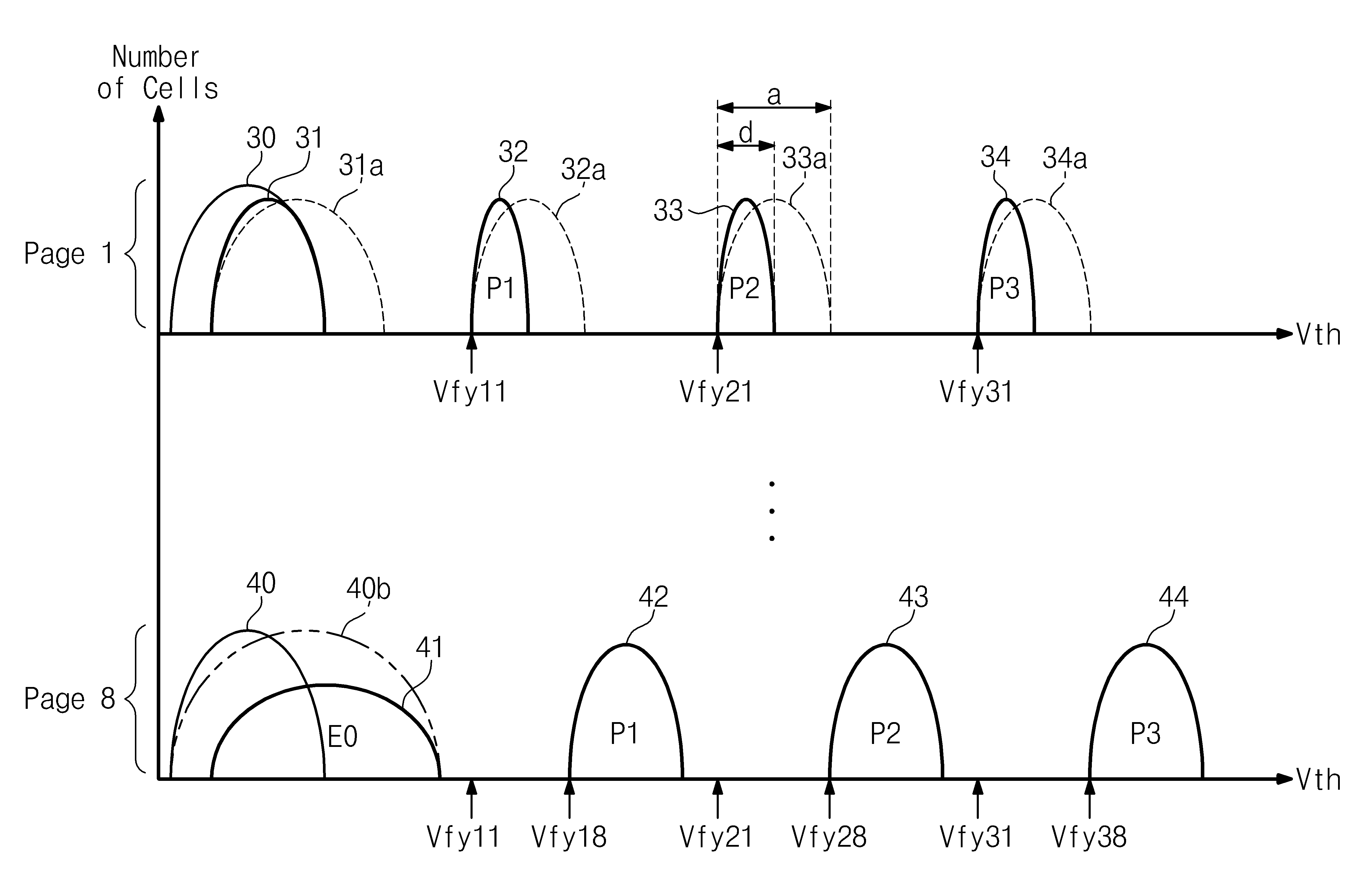
도 7은 도 6의 메모리 블록의 회로 중 하나의 비트 라인 및 이에 연결된 낸드 스트링들을 예시적으로 보여주는 도면이다. 예시적으로, 도 6에서는 제 1 비트 라인(BL<1>) 및 이에 연결된 낸드 스트링들이 도시되어 있다. 설명의 편의상, 하나의 비트 라인에는 8 개의 낸드 스트링들이 연결된다고 가정된다. 또한, 제 1 낸드 스트링(NS<11>)으로부터 제 8 낸드 스트링(NS<81>)으로의 순서로 프로그램 동작이 수행된다고 가정된다.7 is an exemplary illustration of one bit line of the circuit of the memory block of FIG. 6 and the NAND strings connected thereto. Illustratively, in FIG. 6, the first bit line (BL < 1 >) and the NAND strings connected thereto are shown. For convenience of explanation, it is assumed that eight NAND strings are connected to one bit line. It is also assumed that the program operation is performed in order from the first NAND string NS <11> to the eighth NAND string NS <81>.
도 7을 참조하면, 제 1 내지 제 8 낸드 스트링들(NS<11>~NS<81>)은 각각 제 1 내지 제 8 스트링 선택 라인들(SSL<1>~SSL<8>)을 통하여 제 1 비트 라인(BL<1>)에 연결된다. 따라서, 각 낸드 스트링은 비트 라인과 대응하는 스트링 선택 라인의 활성화에 의하여 선택될 수 있다. 예를 들어, 제 1 비트 라인(BL<1>) 및 제 1 스트링 선택 라인(SSL<1>)이 활성화되는 경우, 제 1 낸드 스트링(NS<11>)이 선택될 수 있다. 마찬가지로, 제 1 비트 라인(B<1>) 및 제 2 스트링 선택 라인(SSL<2>)이 활성화되는 경우, 제 2 낸드 스트링(NS<21>)이 선택될 수 있다. Referring to FIG. 7, the first through eighth NAND strings NS <11> through NS <81> are connected to the first through eighth string selection lines SSL <1> through SSL <8> Is connected to one bit line BL <1>. Thus, each NAND string can be selected by activation of a bit line and a corresponding string selection line. For example, when the first bit line BL <1> and the first string selection line SSL <1> are activated, the first NAND string NS <11> can be selected. Similarly, when the first bit line B <1> and the second string select line SSL <2> are activated, the second NAND string NS <21> can be selected.
각각의 페이지들은 제 1 낸드 스트링(NS<11>)에서 제 8 낸드 스트링(NS<81>)으로의 순서로 프로그램된다. 여기서, 페이지는 동일한 워드 라인을 공유하며, 동일한 스트링 선택 라인에 의하여 선택되는 메모리 셀들에 대응한다. 예를 들어, 제 1 페이지(page 1)는 제 1 워드 라인(WL<1>)을 공유하며, 제 1 스트링 선택 라인(SSL<1>)에 의하여 선택되는 메모리 셀들에 대응할 것이다. 마찬가지로, 제 2 페이지(page 2)는 제 1 워드 라인(WL<2>)을 공유하며, 제 2 스트링 선택 라인(SSL<2>)을 공유하는 메모리 셀들에 대응할 것이다.Each page is programmed in order from the first NAND string (NS <11>) to the eighth NAND string (NS <81>). Here, the pages share the same word line and correspond to memory cells selected by the same string selection line. For example, the first page (page 1) would correspond to memory cells that share the first word line (WL < 1 >) and are selected by the first string selection line (SSL < 1 >). Similarly, the second page (page 2) would correspond to memory cells sharing the first word line (WL < 2 >) and sharing the second string selection line (SSL < 2 >).
하나의 메모리 셀이 1 비트의 데이터를 저장하는 경우, 하나의 스트링 선택 라인 및 하나의 워드 라인에 의하여 선택되는 메모리 셀들은 하나의 페이지에 대응할 것이다. 하나의 메모리 셀이 2 비트의 데이터를 저장하는 경우, 하나의 스트링 선택 라인 및 하나의 워드 라인에 의하여 선택되는 메모리 셀들은 두 개의 페이지가 대응할 것이다. 즉, 물리적으로 하나의 워드 라인에 연결된 메모리 셀들은 논리적으로 두 개의 페이지를 형성할 것이다. 이 경우, 두 개의 페이지 중 하나의 페이지는 LSB 데이터를 저장하는 페이지이며, 두 개의 페이지 중 다른 하나의 페이지는 MSB 데이터를 저장하는 페이지일 수 있다. When one memory cell stores one bit of data, the memory cells selected by one string selection line and one word line will correspond to one page. When one memory cell stores two bits of data, the memory cells selected by one string select line and one word line will correspond to two pages. That is, memory cells physically connected to one word line will logically form two pages. In this case, one page of the two pages is a page storing LSB data, and the other page of the two pages may be a page storing MSB data.
계속해서 도 7을 참조하면, 제 1 내지 제 8 페이지들(page 1~page 8)은 각각 제 1 내지 제 8 스트링 선택 라인들(SSL<1>~SSL<8>)에 의하여 선택될 수 있다. 그러나, 제 1 내지 제 8 페이지들(page 1~page 8)은 제 1 워드 라인(WL<1>)을 공유한다. 따라서, 제 1 내지 제 8 페이지들(page 1~page 8) 중 선택된 페이지가 프로그램되는 경우, 비선택된 페이지들도 워드 라인을 통하여 프로그램 전압의 영향에 노출된다. 이는 도 7의 각 페이지에 대한 읽기 마진이 감소함을 의미한다.7, the first to eighth pages (
도 8은 도 7의 제 1 내지 제 8 페이지들(page 1~page 8) 중 제 1 페이지(page 1)에 대한 읽기 마진의 감소를 예시적으로 보여주는 도면이다. 제 1 내지 제 8 페이지들(page 1~page 8) 중 제 1 페이지(page 1)는 가장 먼저 프로그램된다. 따라서, 제 1 페이지(page 1)는 프로그램 동작이 수행된 후에, 제 2 내지 제 8 페이지(page 2~page 8)의 프로그램 동작에 의하여 영향을 받는다. 이하에서는 도 7 및 도 8을 참조하여, 프로그램 디스터브에 의한 제 1 페이지(page 1)의 문턱 전압의 산포의 변화가 예시적으로 설명된다. FIG. 8 is an exemplary diagram illustrating a reduction in read margin for a first page (page 1) of the first through eighth pages (
도 8을 참조하면, 먼저 단계(a)에서, 프로그램 동작이 수행되기 전, 제 1 페이지(page 1)는 초기 상태(initial state, 10)의 문턱 전압의 산포를 갖는다.Referring to FIG. 8, in step (a), before the program operation is performed, the first page (page 1) has a scattering of the threshold voltage of the initial state (10).
이 후, 단계(b)에서, 제 1 페이지(page 1)에 대한 프로그램 동작이 수행된다. 즉, 제 1 페이지(page 1)는 소거 상태(E0, 11), 제 1 프로그램 상태(P1, 12), 제 2 프로그램 상태(P2, 13) 및 제 3 프로그램 상태(P3, 14)로 프로그램된다. Thereafter, in step (b), the program operation for the first page (page 1) is performed. That is, the first page (page 1) is programmed with the erase state E0, 11, the first program state P1, 12, the second program state P2, 13 and the third program state P3, .
이 경우, 예를 들어, 소거 상태(11)는 초기 상태(10)와 실질적으로 동일한 상태일 수 있다. 즉, 제 1 페이지(page 1)의 메모리 셀들 중 소거 상태(11)에 대응하는 메모리 셀들에 대하여는, 프로그램 동작이 수행되지 않을 수 있다. In this case, for example, the erase
다른 예로, 소거 상태(11)는 초기 상태(10)에 비하여 높은 문턱 전압을 갖도록 프로그램될 수도 있다. 즉, 제 1 페이지(page 1)에 대한 프로그램 동작이 수행되는 경우, 소거 상태(11)에 대응하는 메모리 셀들은 초기 상태(10)에 비하여 높은 문턱 전압을 갖도록 프로그램될 수도 있다.As another example, the erase
이 후, 단계(c)에서 제 2 내지 제 8 페이지들(page 2~page 8)에 대한 프로그램 동작이 수행된다. 이 경우, 제 1 페이지(page 1)는 제 1 워드 라인(WL<1>)을 통하여 프로그램 디스터브의 영향을 받는다. 설명의 편의상, 해당 페이지에 대한 프로그램 동작이 수행된 후에 다른 페이지에 대한 프로그램 동작에 의하여 발생하는 디스터브는 프로그램 후 디스터브(Disturb After Program, 이하 DAP))라 칭해진다. Thereafter, a program operation for the second to eighth pages (
제 1 페이지(page 1)의 각 상태의 문턱 전압의 산포는 제 2 내지 제 8 페이지들(page 2~page 8)에 의한 프로그램 후 디스터브(DAP)에 의하여 증가한다. 예를 들어, 단계(c)에 도시된 바와 같이, 소거 상태(E0)의 문턱 전압의 산포는 프로그램 후 디스터브(DAP)에 의하여 "11"에서 "11a"로 증가한다. 마찬가지로, 제 1 프로그램 상태(P1)의 문턱 전압의 산포는 "12"에서 "12a"로 증가한다. The scattering of the threshold voltages of the respective states of the first page (page 1) is increased by post-program disturbance (DAP) by the second to eighth pages (
따라서, 제 1 내지 제 8 페이지들(page 1~page 8) 중 가장 먼저 프로그램 동작이 수행되는 제 1 페이지(page 1)의 읽기 마진은 프로그램 후 디스터브(DAP)에 의하여 감소한다. 예를 들어, 제 1 프로그램 상태(P1)의 문턱 전압의 산포가 "a"에서 "b"로 증가하므로, 제 1 프로그램 상태(P1)와 제 2 프로그램 상태(P2) 사이의 읽기 마진은 감소한다.Accordingly, the read margin of the first page (page 1) in which the program operation is performed first among the first to eighth pages (
특히, 소거 상태(E0)와 제 1 프로그램 상태(P1) 사이의 읽기 마진에 비하여 제 1 프로그램 상태(P1)와 제 2 프로그램 상태(P2) 사이의 읽기 마진이 충분히 확보되지 못한 경우, 제 1 페이지(Page 1)에 대한 읽기 동작 시에 각 프로그램 상태(P1, P2, P3) 사이의 읽기 마진 감소에 의한 읽기 패일(read fail)이 발생할 수 있다. Particularly, when the read margin between the first program state P1 and the second program state P2 is not sufficiently secured as compared with the read margin between the erase state E0 and the first program state P1, A read failure may occur due to the reduction of the read margin between the program states (P1, P2, and P3) during the read operation for the program state (Page 1).
도 9는 도 7의 제 1 내지 제 8 페이지들(page 1~page 8) 중 제 8 페이지(page 8)에 대한 읽기 마진의 감소를 예시적으로 보여주는 도면이다. 제 1 내지 제 8 페이지들(page 1~page 8) 중 제 8 페이지(page 8)는 가장 나중에 프로그램된다. 따라서, 제 8 페이지(page 8)는 프로그램 동작이 수행되기 전에, 제 1 내지 제 7 페이지(page 1~page 7)의 프로그램 동작에 의하여 영향을 받는다. 이하에서는 도 7 및 도 9을 참조하여, 프로그램 디스터브에 의한 제 8 페이지(page 8)의 문턱 전압의 산포의 변화가 예시적으로 설명된다.FIG. 9 is a diagram illustrating a reduction in the read margin for the eighth page (page 8) among the first through eighth pages (
도 9를 참조하면, 먼저 단계(a)에서, 프로그램 동작이 수행되기 전, 제 1 페이지(page 1)는 초기 상태(initial state, 20)의 문턱 전압의 산포를 갖는다.Referring to FIG. 9, in step (a), before the program operation is performed, the first page (page 1) has a scattering of the threshold voltage of the initial state (20).
이 후, 단계(b)에서, 제 8 페이지(page 8)에 대한 프로그램 동작이 수행되기 전, 제 1 내지 제 7 페이지들(page 1~page 7)에 대한 프로그램 동작이 수행된다. 이 경우, 제 8 페이지(page 8)는 제 1 워드 라인(WL<1>)을 통하여 프로그램 디스터브의 영향을 받는다. Thereafter, in step (b), the program operation for the first to seventh pages (
설명의 편의상, 해당 페이지에 대한 프로그램 동작이 수행되기 전에 다른 페이지에 대한 프로그램 동작에 의하여 발생하는 디스터브는 프로그램 전 디스터브(Disturb Before Program, 이하 DBP)이라 칭해진다. 프로그램 전 디스터브(DBP)에 의하여, 제 8 페이지(page 8)의 초기 상태의 문턱 전압의 산포는 "20"에서 "20b"로 증가한다. For convenience of explanation, a disturb caused by a program operation on another page before a program operation on the page is performed is called a disturb before program (DBP). By the pre-program disturbance DBP, the dispersion of the threshold voltage in the initial state of the eighth page (page 8) increases from "20" to "20b".
이 후, 단계(c)에서, 제 8 페이지(page 8)에 대한 프로그램 동작이 수행된다. 즉, 제 8 페이지(page 8)는 소거 상태(E0, 21), 제 1 프로그램 상태(P1, 22), 제 2 프로그램 상태(P2, 23), 제 3 프로그램 상태(P3, 24)로 프로그램된다. Thereafter, in step (c), the program operation for the eighth page (page 8) is performed. That is, the eighth page (page 8) is programmed to the erase state E0, 21, the first program state P1, 22, the second program state P2, 23 and the third program state P3, 24 .
이 경우, 예를 들어, 소거 상태(21)와 초기 상태(20b)는 실질적으로 동일한 상태일 수 있다. 즉, 제 8 페이지(page 8)의 메모리 셀들 중 소거 상태(21)에 대응하는 메모리 셀들에 대하여는, 프로그램 동작이 수행되지 않을 수 있다. In this case, for example, the erase
다른 예로, 소거 상태(21)는 초기 상태(20b)에 비하여 높은 문턱 전압을 갖도록 프로그램될 수도 있다. 즉, 제 8 페이지(page 8)에 대한 프로그램 동작이 수행되는 경우, 소거 상태(21)에 대응하는 메모리 셀들은 초기 상태(20b)에 비하여 높은 문턱 전압을 갖도록 프로그램될 수도 있다.As another example, the erase
한편, 제 8 페이지(page 8)는 가장 나중에 프로그램되기 때문에, 프로그램 후 디스터브(DAP)에 의한 영향은 받지 않는다. 따라서, 단계(c)에 도시된 바와 같이, 제 1 내지 제 3 프로그램 상태(P1~P3, 22~23)의 문턱 전압의 산포는 충분한 읽기 마진을 갖는다.On the other hand, since the eighth page (page 8) is programmed last, it is not influenced by the post-program disturbance (DAP). Thus, as shown in step (c), the scattering of the threshold voltages of the first to third programmed states P1 to P3, 22 to 23 has a sufficient read margin.
그러나, 프로그램 전 디스터브(DBP)에 의하여 제 8 페이지(page 8)의 초기 상태는 넓은 문턱 전압 윈도우를 가지므로, 프로그램 동작이 수행된 후에 제 8 페이지(page 8)의 초기 상태(E0)는 "c"에 해당하는 넓은 문턱 전압 윈도우를 갖는다. 즉, 제 8 페이지(page 8)의 초기 상태(E0, 21)와 제 1 프로그램 상태(P1, 22) 사이의 읽기 마진이 감소한다. 이는 제 1 페이지(Page 1)에 대한 읽기 동작 시에, 소거 상태(E0)와 제 1 프로그램 상태(P1) 사이의 읽기 마진 감소에 의한 읽기 패일이 발생할 수 있음을 의미한다. However, since the initial state of the eighth page (page 8) by the program pre-disturb (DBP) has a wide threshold voltage window, the initial state E0 of the eighth page (page 8) quot; c ". That is, the read margin between the initial state (E0, 21) of the eighth page (page 8) and the first program state (P1, 22) decreases. This means that during the read operation for the first page (Page 1), a read failure due to the reduction of the read margin between the erase state E0 and the first program state P1 may occur.
도 10은 도 7의 제 1 내지 제 8 페이지들(page 1~page 8)에 대한 프로그램 동작이 순차적으로 수행된 경우에, 각 페이지의 문턱 전압의 산포를 예시적으로 보여주는 도면이다. 이하에서는 도 7 내지 도 10을 참조하여, 프로그램 순서에 따른 문턱 전압 산포의 변화가 설명된다.FIG. 10 is a diagram showing an exemplary dispersion of the threshold voltages of the respective pages when the program operation for the first to eighth pages (
도 10을 참조하면, 제 1 및 제 2 페이지(page 1, page 2)는 다른 페이지들에 비하여 빨리 프로그램된다. 따라서, 도 8에서 설명된 바와 같이, 제 1 및 제 2 페이지(page 1, page 2)는 제 7 및 제 8 페이지(page 7, page 8)에 비하여 프로그램 후 디스터브(DAP)의 영향을 많이 받는다.Referring to FIG. 10, the first and second pages (
예를 들어, 제 1 페이지(page 1)는 제 2 내지 제 8 페이지(page 2~page 8)에 대한 프로그램 동작에 의하여, 7 번의 프로그램 후 디스터브(DAP)의 영향을 받는다. 또한, 제 2 페이지(page 2)는 제 1 페이지(page 1)의 프로그램 동작에 의하여 1 번의 프로그램 전 디스터브(DBP)의 영향을 받고, 6 번의 프로그램 후 디스터브(DAP)의 영향을 받는다. 이 경우, 도 10에 도시된 바와 같이, 제 1 및 제 2 페이지(page 1, page 2)의 문턱 전압의 산포는 증가된다. 특히, 소거 상태(E0)와 제 1 프로그램 상태(P1) 사이에 충분한 읽기 마진이 확보된 경우, 도 10에 도시된 바와 같이, 제 1 내지 제 3 프로그램 상태(P1~P3) 사이의 읽기 마진 감소로 인한 읽기 패일이 발생할 수 있다.For example, the first page (page 1) is influenced by the program post-program disturb (DAP) by the program operation for the second to eighth pages (
한편, 제 7 및 제 8 페이지(page 7, page 8)는 다른 페이지들에 비하여 나중에 프로그램된다. 따라서, 도 9에서 설명된 바와 같이, 제 7 및 제 8 페이지(page 7, page 8)는 제 1 및 제 2 페이지(page 1, page 2)에 비하여 프로그램 전 디스터브(DBP)의 영향을 많이 받는다. On the other hand, the seventh and eighth pages (
예를 들어, 제 7 페이지(page 7)는 제 1 내지 제 6 페이지(pgae 1~page 6)에 의하여 6 번의 프로그램 전 디스터브(DBP)의 영향을 받고, 제 8 페이지(page 8)에 의하여 1 번의 프로그램 후 디스터브(DAP)의 영향을 받는다. 또한, 제 8 페이지(pgae 8)는 제 1 내지 제 7 페이지(page 1~page 7)에 의하여 7 번의 프로그램 전 디스터브(DBP)의 영향을 받는다. 이 경우, 도 10에 도시된 바와 같이, 소거 상태(E0)와 제 1 프로그램 상태(P1) 사이의 읽기 마진 감소로 인한 읽기 패일이 발생할 수 있다.For example, the seventh page (page 7) is affected by six program pre-disturbances (DBP) by the first to sixth pages (
도 8 내지 도 10에서 설명된 바와 같이, 동일한 워드 라인을 공유하는 페이지들 중 먼저 프로그램 동작이 수행되는 페이지는 다른 페이지들에 비하여 프로그램 후 디스터브(DAP)의 영향을 많이 받는다. 이 경우, 프로그램 상태들 사이의 읽기 마진 감소로 인한 읽기 패일이 주로 문제될 수 있다.As described in FIGS. 8 to 10, among the pages sharing the same word line, the page on which the program operation is first performed is more affected by post-program disturbance (DAP) than the other pages. In this case, read failures due to reduced read margins between program states can be a major problem.
이와 반대로, 동일한 워드 라인을 공유하는 페이지들 중 나중에 프로그램 동작이 수행되는 페이지는 다른 페이지들에 비하여 프로그램 전 디스터브(DBP)의 영향을 많이 받는다. 이 경우, 소거 상태와 인접한 프로그램 상태 사이의 읽기 마진 감소로 인한 읽기 패일이 주로 문제될 수 있다.On the contrary, among the pages sharing the same word line, the page where the program operation is performed later is more influenced by the pre-program disturbance (DBP) than the other pages. In this case, a read failure due to a reduction in read margin between the erase state and the adjacent program state may be a problem in the main.
이러한, 문제를 해결하기 위하여, 본 발명의 실시 예에 따른 불휘발성 메모리 장치(100)는 프로그램 순서에 따라 서로 다른 프로그램 스킴 및 읽기 스킴을 적용한다. 따라서, 프로그램 후 디스터브(DAP) 또는 프로그램 전 디스터브(DBP)에 의한 읽기 패일을 방지할 수 있다. 이는 이하의 도 11 내지도 19를 통하여 좀더 자세히 설명될 것이다. In order to solve such a problem, the
한편, 설명의 편의상, 도 10에서는, 소거 상태(erase state)는 초기 상태(또는, 디스터브의 영향을 받은 초기 상태)에 비하여 높은 문턱 전압을 갖는 것으로 도시되었다. 다만 이는 예시적인 것이며, 도 8 및 도 9에서 설명된 바와 같이, 소거 상태는 초기 상태(또는, 디스터브의 영향을 받은 초기 상태)와 실질적으로 동일한 상태일 수 있다. For convenience of explanation, in FIG. 10, the erase state is shown to have a higher threshold voltage than the initial state (or the initial state affected by disturb). However, this is merely an example, and the erase state may be substantially the same as the initial state (or the initial state affected by the disturb), as illustrated in FIGS. 8 and 9.
도 11은 본 발명의 일 실시 예에 따른 프로그램 동작을 보여주는 도면이다. 도 11에서는 다른 페이지들에 비하여 빨리 프로그램되는 페이지에 대한 읽기 패일을 방지하는 프로그램 방법이 설명된다. 설명의 편의상, 도 11에서는 제 1 페이지(page 1) 및 제 8 페이지(page 8)를 서로 대비하여, 본 발명의 실시 예에 따른 프로그램 동작이 설명된다. 이하에서는 도 7 및 도 11을 참조하여, 본 발명의 실시 예에 따른 프로그램 동작이 설명된다. 11 is a diagram illustrating a program operation according to an embodiment of the present invention. In Fig. 11, a program method for preventing a read failure to a page that is programmed faster than other pages is described. For convenience of explanation, the program operation according to the embodiment of the present invention will be described with reference to FIG. 11 in comparison with the first page (page 1) and the eighth page (page 8). Hereinafter, the program operation according to the embodiment of the present invention will be described with reference to Figs. 7 and 11. Fig.
도 11을 참조하면, ISPP 스킴(Incremental Step Pulse Program)에 의하여 프로그램 동작이 수행된다. 제 1 페이지(page 1)에 대한 프로그램 동작이 수행되는 경우, 제 1 워드 라인(WL<1>)에는 "△Va"에 해당하는 문턱 전압의 증가분을 갖는 프로그램 전압들이 제공된다. 이에 반하여, 제 8 페이지(page 8)에 대한 프로그램 동작이 수행되는 경우, 제 1 워드 라인(WL<1>)에는 "△Va 보다 큰 "△Vb"에 해당하는 문턱 전압의 증가분을 갖는 프로그램 전압들이 제공된다. Referring to FIG. 11, a program operation is performed by an ISPP scheme (Incremental Step Pulse Program). When a program operation for the first page (page 1) is performed, the first word line (WL < 1 >) is provided with program voltages having an increment of the threshold voltage corresponding to " DELTA Va ". On the other hand, when the program operation for the
제 1 페이지(page 1)의 문턱 전압의 증가분이 제 8 페이지(page 8)의 문턱 전압의 증가분보다 작게 설정됨으로써, 제 1 페이지(page 1)의 문턱 전압 윈도우는 제 8 페이지(page 8)에 비하여 작게 형성될 수 있다. 이는 비록 제 1 페이지(page 1)가 프로그램 후 디스터브(DAP)의 영향을 받는다고 할지라도, 충분한 읽기 마진이 확보될 수 있음을 의미한다. The threshold voltage window of the first page (page 1) is set to be smaller than the increment of the threshold voltage of the eighth page (page 8), so that the threshold voltage window of the first page (page 1) Can be formed small. This means that a sufficient read margin can be secured even if the first page (page 1) is affected by post-program disturbance (DAP).
도 12는 본 발명의 일 실시 예에 따른 프로그램 동작을 보여주는 도면이다. 도 12에서는 다른 페이지들에 비하여 느리게 프로그램되는 페이지에 대한 읽기 패일을 방지하는 프로그램 방법이 설명된다. 설명의 편의상, 도 11과 유사하게, 제 1 페이지(page 1)에 대응하는 문턱 전압의 증가분은 제 8 페이지(page 8)에 대응하는 문턱 전압의 증가분보다 작다고 가정된다. 또한, 도 11과 유사하게, 제 1 페이지(page 1) 및 제 8 페이지(page 8)를 서로 대비하여, 본 발명의 실시 에에 따른 프로그램 동작이 설명된다. 12 is a diagram illustrating a program operation according to an embodiment of the present invention. In Fig. 12, a program method for preventing a read failure to a page that is programmed slowly compared to other pages is described. 11, it is assumed that the increment of the threshold voltage corresponding to the first page (page 1) is smaller than the increment of the threshold voltage corresponding to the eighth page (page 8). Similar to Fig. 11, the program operation according to the embodiment of the present invention will be described by comparing the first page (page 1) and the eighth page (page 8) with each other.
도 12를 참조하면, 복수의 프로그램 루프를 포함하는 ISPP 스킴에 의하여 프로그램 동작이 수행된다. 예시적으로, 제 1 페이지(page 1)에 대한 프로그램 동작은 "k" 개의 루프들로 구성되며, 제 8 페이지(page 8)에 대한 프로그램 동작은 "i" 개의 루프들로 구성된다고 가정된다. 또한, 각 루프는 1 개의 프로그램 전압과 1 개의 검증 읽기 전압으로 구성된다고 가정된다. 다만, 이는 예시적인 것이며, 제 1 및 제 8 페이지(page 1, page 8)에 대한 프로그램 동작은 동일한 횟수의 루프들을 통하여 수행될 수 있다. 또한, 각 루프는 복수 개의 프로그램 전압 및 복수 개의 검증 읽기 전압들로 구성될 수 있다. Referring to FIG. 12, a program operation is performed by an ISPP scheme including a plurality of program loops. Illustratively, it is assumed that the program operation for the first page (page 1) consists of "k" loops, and that the program operation for the eighth page (page 8) consists of "i" loops. It is also assumed that each loop consists of one program voltage and one verify read voltage. However, this is an example, and the program operation for the first and eighth pages (
제 1 페이지(page 1)에 대한 프로그램 동작이 수행되는 경우, 제 1 페이지(page 1)에는 제 1 검증 읽기 전압(Vfy11)이 제공된다. 이에 반하여, 제 8 페이지(page 8)에 대한 프로그램 동작이 수행되는 경우, 제 8 페이지(page 8)에는 제 1 페이지(page 1)의 제 1 검증 읽기 전압(Vfy11)보다 높은 제 1 검증 읽기 전압(Vfy18)이 제공된다. When a program operation for the first page (page 1) is performed, a first verify read voltage (Vfy11) is provided on the first page (page 1). On the other hand, when the program operation for the
여기서, 제 1 페이지(page 1)의 제 1 검증 읽기 전압(Vfy11)은 제 1 페이지(page 1)의 제 1 프로그램 상태(P1, 도 10)에 대한 검증 읽기 전압을 의미하고, 제 8 페이지(page 8)의 제 1 검증 읽기 전압(Vfy18)은 제 8 페이지(page 8)의 제 1 프로그램 상태(P1, 도 10)에 대한 검증 읽기 전압을 의미한다. Here, the first verify read voltage Vfy11 of the first page (page 1) means the verify read voltage for the first program state (P1, Fig. 10) of the first page (page 1) The first verify read voltage Vfy18 of
제 8 페이지(page 8)의 제 1 검증 읽기 전압(Vfy18)이 제 1 페이지(page 1)의 제 1 검증 읽기 전압(Vfy11)보다 작게 설정됨으로써, 제 8 페이지(page 8)의 소거 상태(E0)와 제 1 프로그램 상태(P1) 사이의 읽기 마진은 제 1 페이지(page 1)에 비하여 넓게 형성될 수 있다. 이는 비록 제 8 페이지(page 8)가 프로그램 전 디스터브(DBP)의 영향을 받는다고 할지라도, 충분한 읽기 마진이 확보될 수 있음을 의미한다. The first verify read voltage Vfy18 of the eighth page (page 8) is set to be smaller than the first verify read voltage Vfy11 of the first page (page 1), so that the erase state E0 ) And the first program state P1 can be formed wider than the first page (page 1). This means that a sufficient read margin can be ensured even though the eighth page (page 8) is affected by pre-program disturbance (DBP).
도 13은 도 11 및 도 12의 프로그램 스킴에 의하여 프로그램된 제 1 및 제 8 페이지(page 1, page 8)의 문턱 전압의 산포를 보여주는 도면이다. 도 13에서, "30" 및 "40"은 각각 제 1 페이지(page 1)와 제 8 페이지(page 8)의 초기 상태의 문턱 전압의 산포를 의미한다. "31, 32, 33, 34"과 "41, 42, 43, 44"는 각각 제 1 페이지(page 1)와 제 8 페이지(page 8)에 대한 프로그램 동작이 수행된 경우의 문턱 전압의 산포를 의미한다. "31a, 32a, 33a, 34a"는 프로그램 후 디스터브(DAP)에 의한 제 1 페이지(page 1)의 문턱 전압의 증가를 의미한다. "40b"는 프로그램 전 디스터브(DBP)에 의한 제 8 페이지(page 8)의 문턱 전압의 증가를 의미한다. FIG. 13 is a diagram showing the distribution of threshold voltages of the first and eighth pages (
도 11에서 설명된 바와 같이, 제 1 페이지(page 1)에 대한 프로그램 동작 시의 문턱 전압의 증가분은 제 8 페이지(page 8)에 대한 프로그램 동작 시의 문턱 전압의 증가분보다 작다. 따라서, 도 13에 도시된 바와 같이, 제 1 페이지(page 1)에 대한 프로그램 동작이 수행되면, 제 1 페이지(page 1)의 문턱 전압 윈도우는 제 8 페이지(page 8)의 문턱 전압 윈도우보다 작게 설정될 수 있다. 11, the increment of the threshold voltage in the program operation for the first page (page 1) is smaller than the increment of the threshold voltage in the program operation for the eighth page (page 8). 13, when the program operation for the first page (page 1) is performed, the threshold voltage window of the first page (page 1) is smaller than the threshold voltage window of the eighth page (page 8) Can be set.
이 경우, 제 2 내지 제 8 페이지들(page 2~page 8)의 프로그램 동작으로 인한 프로그램 후 디스터브(DAP)에 의하여 제 1 페이지(page 1)의 문턱 전압 윈도우가 "d"에서 "a"로 넓어진다고 할지라도, 제 1 페이지(page 1)의 각 프로그램 상태들(P1~P3) 사이에는 충분한 읽기 마진이 확보될 수 있다. 따라서, 프로그램 후 디스터브(DAP)에 의한 읽기 실패가 방지될 수 있다.In this case, the threshold voltage window of the first page (page 1) changes from "d" to "a" by post-program disturbance (DAP) due to program operation of the second to eighth pages Even if it is widened, a sufficient read margin can be ensured between the program states P1 to P3 of the first page (page 1). Therefore, read failure by the post-program disturb (DAP) can be prevented.
또한, 도 12에서 설명된 바와 같이, 제 8 페이지(page 8)의 검증 읽기 전압(Vfy18)의 레벨은 제 1 페이지(page 1)의 검증 읽기 전압(Vfy11)의 레벨보다 높다. 따라서, 도 13에 도시된 바와 같이, 제 8 페이지(page 8)의 제 1 프로그램 상태(P1)는 제 1 페이지(page 1)의 제 1 프로그램 상태(P1)보다 높은 문턱 전압을 갖도록 형성될 수 있다. 12, the level of the verify read voltage Vfy18 of the eighth page (page 8) is higher than the level of the verify read voltage Vfy11 of the first page (page 1). 13, the first program state P1 of the eighth page (page 8) can be formed to have a higher threshold voltage than the first program state P1 of the first page (page 1) have.
이 경우, 제 1 내지 제 7 페이지들(page 1~page 7)의 프로그램 동작으로 인한 프로그램 전 디스터브(DBP)에 의하여 소거 상태(E0)의 문턱 전압 윈도우가 넓어진다고 할지라도, 소거 상태(E1)와 제 1 프로그램 상태(P1) 사이에는 충분한 읽기 마진이 확보될 수 있다. 다라서, 프로그램 전 디스터브(DBP)에 의한 읽기 실패가 방지될 수 있다.In this case, even if the threshold voltage window of the erase state E0 is widened by the program pre-disturbance DBP due to the program operation of the first to seventh pages (
한편, 도 13에 도시된 바와 같이, 제 8 페이지(page 8)의 제 2 검증 읽기 전압(Vfy28)을 제 1 페이지(page 1)의 제 2 검증 읽기 전압(Vfy21)보다 높게 설정하고, 제 8 페이지(page 8)의 제 3 검증 읽기 전압(Vfy38)을 제 1 페이지(page 1)의 제 3 검증 읽기 전압(Vfy31)보다 높게 설정함으로써, 제 8 페이지(page 8)의 프로그램 상태들(42, 43, 44) 사이의 읽기 마진이 확보될 수 있다. On the other hand, as shown in Fig. 13, the second verify read voltage Vfy28 of the eighth page (page 8) is set higher than the second verify read voltage Vfy21 of the first page (page 1) By setting the third verify read voltage Vfy38 of the
도 11 내지 도 13을 참조하여 설명된 바와 같이, 본 발명의 기술적 사상에 따른 불휘발성 메모리 장치(100, 도 1 참조)는 동일한 워드 라인을 공유하는 복수의 페이지들의 프로그램 순서에 따라 서로 다른 프로그램 스킴을 적용함으로써, 읽기 마진 감소로 인한 읽기 실패를 방지할 수 있다. 다만, 도 11 내지 도 13의 프로그램 스킴은 예시적인 것이며, 본 발명의 기술적 사상은 다양한 방식으로 적용될 수 있다.As described with reference to Figs. 11 to 13, the nonvolatile memory device 100 (see Fig. 1) according to the technical idea of the present invention is a nonvolatile memory device It is possible to prevent the reading failure due to the reduction of the reading margin. However, the program schemes of Figs. 11 to 13 are illustrative, and the technical idea of the present invention can be applied in various ways.
도 14는 본 발명의 다른 실시 예에 따른 프로그램 동작을 보여주는 도면이다. 설명의 편의상, 도 14에서는 도 11과 유사하게, 제 1 페이지(page 1)의 문턱 전압의 증가분이 제 8 페이지(page 8)의 문턱 전압의 증가분보다 작다고 가정된다. 또한, 도 12와 유사하게, 제 8 페이지(page 8)의 검증 읽기 전압의 레벨이 제 1 페이지(page 1)의 검증 읽기 전압의 레벨보다 크다고 가정된다.FIG. 14 is a diagram illustrating a program operation according to another embodiment of the present invention. For convenience of explanation, in FIG. 14, it is assumed that the increment of the threshold voltage of the first page (page 1) is smaller than the increment of the threshold voltage of the page 8 (page 8), similarly to FIG. 12, it is assumed that the level of the verify read voltage of the eighth page (page 8) is larger than the level of the verify read voltage of the first page (page 1).
도 14를 참조하면, 제 1 페이지(page 1)에 대한 프로그램 동작 시에 제공되는 제 1 프로그램 전압(Vpgm 1)의 레벨이 제 8 페이지(page 8)에 대한 프로그램 동작 시에 제공되는 제 1 프로그램 전압(Vpgm 1)의 레벨보다 높다. 이는 제 8 페이지(page 8)에 비하여 작게 설정된 문턱 전압의 증가분에 의하여, 프로그램 동작이 수행되는 시간이 길어짐을 방지하기 위함이다.14, when the level of the first
좀더 자세히 설명하면, 제 1 페이지(page 1)의 문턱 전압의 증가분이 제 8 페이지(page 8)의 문턱 전압의 증가분보다 낮게 설정되었으므로, 제 1 페이지(page 1)에 대한 프로그램 동작에 소요되는 시간이 제 8 페이지(page 8)에 대한 프로그램 동작에 소요되는 시간보다 길어질 수 있다. 이를 방지하기 위하여, 도 14에서는, 제 1 페이지(page 1)에 대한 프로그램 동작이 시작되는 프로그램 전압의 레벨을 제 8 페이지(page 8)에 대한 프로그램 동작이 시작되는 프로그램 전압의 레벨보다 높게 설정할 수 있다. More specifically, since the increment of the threshold voltage of the first page (page 1) is set to be lower than the increment of the threshold voltage of the eighth page (page 8), the time required for the program operation for the first page May be longer than the time required for the program operation for the eighth page (page 8). In order to prevent this, it is possible to set the level of the program voltage at which the program operation for the first page (page 1) is started to be higher than the level of the program voltage at which the program operation for the eighth page (page 8) have.
따라서, 제 1 루프(Loop 1)에 의하여 증가되는 문턱 전압을 높게 설정함으로써, 낮은 문턱 전압의 증가분에 의하여 제 1 페이지(page 1)에 대한 프로그램 동작에 소요되는 시간이 길어지는 것을 방지할 수 있다. Therefore, by setting the threshold voltage increased by the first loop (Loop 1) to be high, it is possible to prevent the time required for the program operation for the first page (page 1) from being prolonged by the increase of the low threshold voltage .
도 15는 본 발명의 다른 실시 예에 따른 프로그램 동작을 보여주는 도면이다. 설명의 편의상, 도 15에서는 도 13과 유사하게, 제 1 페이지(page 1)에 대한 문턱 전압의 산포와 제 8 페이지(page 8)에 대한 문턱 전압의 산포가 서로 대비적으로 설명된다. 15 is a diagram illustrating a program operation according to another embodiment of the present invention. For convenience of explanation, in FIG. 15, similar to FIG. 13, the scattering of the threshold voltage for the first page (page 1) and the scattering of the threshold voltage for the page 8 (page 8) are described in comparison with each other.
도 13에서 설명된 바와 같이, 제 1 페이지(page 1)의 문턱 전압 윈도우는 제 8 페이지(page 8)에 비하여 작게 형성된다. 또한, 제 8 페이지(page 8)의 각 프로그램 상태의 문턱 전압의 레벨은 제 1 페이지(page 1)의 각 프로그램 상태의 문턱 전압의 레벨보다 높게 설정된다. As described in Fig. 13, the threshold voltage window of the first page (page 1) is formed smaller than the eighth page (page 8). The level of the threshold voltage of each program state of the eighth page (page 8) is set to be higher than the level of the threshold voltage of each program state of the first page (page 1).
이 경우, 도 15에 도시된 바와 같이, 제 1 페이지(page 1)에 대한 프로그램 동작이 수행될 때, 제 1 워드 라인(WL<1>, 도 7 참조)을 제외한 비선택된 워드 라인들(즉, WL<2>~WL<8>, 도 7 참조)에는 제 1 패스 전압(Vpass1)이 제공될 수 있다. 반면, 제 8 페이지(page 8)에 대한 프로그램 동작이 수행될 때, 제 1 워드 라인(WL<1>)을 제외한 비선택된 워드 라인들에는 제 1 패스 저압(Vpass1)보다 "e"만큼 높은 제 8 패스 전압(Vpass8)이 제공될 수 있다. In this case, as shown in FIG. 15, when the program operation for the first page (page 1) is performed, the non-selected word lines (i.e., word lines) other than the first word line , WL <2> to WL <8>, see FIG. 7) may be provided with a first pass voltage Vpass1. On the other hand, when the program operation for
즉, 동일한 워드 라인을 공유하는 복수의 페이지들 중 먼저 프로그램되는 경우에 제공되는 패스 전압의 레벨은 나중에 프로그램되는 경우에 제공되는 패스 전압의 레벨보다 낮게 설정될 수 있다. That is, the level of the path voltage provided in the case of first being programmed among the plurality of pages sharing the same word line may be set to be lower than the level of the path voltage provided in case of later programming.
도 16은 본 발명의 실시 예에 따른 프로그램 동작을 보여주는 순서도이다. 이하에서는 도 1을 참조하여, 본 발명의 불휘발성 메모리 장치(100)의 프로그램 동작이 설명된다.16 is a flowchart showing a program operation according to an embodiment of the present invention. Hereinafter, the program operation of the
S110 단계에서, 제어 로직(150)은 외부로부터 프로그램 명령(PGM_CMD) 및 어드레스(ADDR)를 수신한다.In step S110, the
S120 단계에서, 제어 로직(150)은 동일한 워드 라인을 공유하는 복수의 페이지들 중 해당 어드레스에 대응하는 스트링 선택 라인(SSL)을 선택한다.In step S120, the
S130 단계에서, 제어 로직(150)은 선택된 스트링 선택 라인의 위치에 따라 프로그램 스킴을 조정한다. 예를 들어, 도 7에 도시된 바와 같이, 스트링 선택 라인의 위치에 따라 프로그램 순서가 결정되는 경우, 제어 로직(150)은 선택된 스트링 선택 라인의 위치에 따라, 해당하는 페이지의 프로그램 순서를 판단할 수 있다.In step S130, the
제어 로직(150)은 선택된 스트링 선택 라인의 위치에 따라 서로 다른 문턱 전압의 증가분을 갖는 프로그램 전압들을 생성하도록, 프로그램 스킴을 조정할 수 있다. 다른 예로, 제어 로직(150)은 프로그램 순서에 따라 서로 다른 레벨의 검증 읽기 전압을 갖도록, 프로그램 스킴을 조정할 수 있다.
S140 단계에서, 조정된 프로그램 스킴에 따라 프로그램 동작이 수행된다. 예를 들어, 해당 페이지가 동일한 워드 라인을 공유하는 다른 페이지들에 비하여 먼저 프로그램되는 경우, 제어 로직(120)은 낮은 문턱 전압의 증가분을 갖는 프로그램 전압들을 생성하도록 전압 발생기(120)를 제어할 것이다. 이 후, 조정된 프로그램 전압에 의한 프로그램 동작이 수행될 것이다. In step S140, the program operation is performed according to the adjusted program scheme. For example, if the page is first programmed relative to other pages sharing the same word line, the
다른 예로, 해당 페이지가 동일한 워드 라인을 공유하는 다른 페이지들에 비하여 나중에 프로그램되는 경우, 제어 로직(120)은 높은 검증 읽기 전압을 생성하도록 전압 발생기(120)를 제어할 것이다. 이 후, 조정된 검증 읽기 전압에 의한 프로그램 동작이 수행될 것이다.As another example, if the page is later programmed relative to other pages sharing the same word line, the
도 17은 본 발명의 다른 실시 예에 따른 프로그램 동작을 보여주는 순서도이다. 이하에서는 도 1을 참조하여, 본 발명의 불휘발성 메모리 장치(100)의 프로그램 동작이 설명된다.17 is a flowchart showing a program operation according to another embodiment of the present invention. Hereinafter, the program operation of the
S210 단계에서, 제어 로직(150)은 외부로부터 프로그램 명령(PGM_CMD) 및 어드레스(ADDR)를 수신한다.In step S210, the
S220 단계에서, 제어 로직(150)은 동일한 워드 라인을 공유하는 복수의 페이지들 중 해당 어드레스에 대응하는 페이지의 스트링 선택 라인(SSL)의 위치를 탐지한다. 즉, 도 7에 도시된 바와 같이, 스트링 선택 라인의 위치에 따라 프로그램 순서가 결정되는 경우, 제어 로직(150)은 선택된 스트링 선택 라인의 위치에 따라, 해당하는 페이지의 프로그램 순서를 판단할 수 있다.In step S220, the
S230 단계에서, 제어 로직(150)은 해당 페이지의 스트링 선택 라인(SSL)의 위치가 기준 스트링 선택 라인의 위치에 선행하는지의 여부를 판단한다. 즉, 도 7에 도시된 바와 같이, 스트링 선택 라인의 위치에 따라 프로그램 순서가 결정되는 경우, 제어 로직(150)은 해당 페이지의 스트링 선택 라인(SSL)의 위치를 기준 스트링 선택 라인의 위치와 비교함으로써, 해당 페이지가 기준 스트링 선택 라인의 페이지보다 먼저 프로그램되는 지의 여부를 판단한다. In step S230, the
여기서, 기준 스트링 선택 라인의 위치는 프로그램 전 디스터브(DBP)와 프로그램 후 디스터브(DAP)의 영향 중 어느 디스터브의 영향을 많이 받는지를 결정하는 기준이 되는 순서를 의미한다. 예를 들어, 제 1 내지 제 8 페이지(page 1~page 8)에 대한 프로그램 동작이 순차적으로 수행되는 경우, 기준 스트링 선택 라인의 위치는 제 4 페이지(page 4)에 대응하는 스트링 선택 라인의 위치 또는 제 5 페이지(page 8)에 대응하는 스트링 선택 라인의 위치가 될 것이다. 또한, 이 경우, 제 4 페이지(page 4) 또는 제 5 페이지(page 5)는 기준 페이지라 칭해질 수 있다. Here, the position of the reference string selection line means a sequence which is a criterion for determining which disturbance is influenced by pre-program disturbance DBP and post-program disturbance DAP. For example, when the program operations for the first to eighth pages (
해당 페이지의 스트링 선택 라인의 위치가 기준 스트링 선택 라인의 위치에 선행하는 경우(즉, 해당 페이지가 기준 페이지보다 먼저 프로그램되는 경우), ISPP의 문턱 전압의 증가분은 해당 페이지의 스트링 선택 라인의 위치가 기준 스트링 선택 라인의 위치에 후행하는 경우에 비하여 작게 설정된다(S240 단계). 이는 문턱 전압의 증가분을 낮게 설정함으로써, 해당 페이지의 문턱 전압 윈도우를 작게 형성하기 위함이다.If the position of the string selection line of the page precedes the position of the reference string selection line (i.e., if the page is programmed prior to the reference page), the increase in the threshold voltage of the ISPP is determined by the position of the string selection line Is set to be smaller than the case of trailing at the position of the reference string selection line (step S240). This is to reduce the threshold voltage window of the page by setting the increment of the threshold voltage to be low.
해당 페이지의 스트링 선택 라인의 위치가 기준 스트링 선택 라인의 위치에 후행하는 경우(즉, 해당 페이지가 기준 페이지보다 늦게 프로그램되는 경우), 검증 읽기 전압의 레벨은 해당 페이지의 스트링 선택 라인의 위치가 기준 스트링 선택 라인의 위치에 선행하는 경우에 비하여 높게 설정된다(S250 단계). 이는 검증 읽기 전압을 높게 설정함으로써, 소거 상태와 인접하는 프로그램 상태 사이의 읽기 마진을 확보하기 위함이다.If the position of the string selection line of the page is behind the position of the reference string selection line (i.e., if the page is programmed later than the reference page), the level of the verify read voltage is determined by the position of the string selection line Is set to be higher than that in the case of preceding the position of the string selection line (step S250). This is to ensure a read margin between the erase state and the adjacent program state by setting the verify read voltage high.
이 후, S260 단계에서, 조정된 스킴을 이용하여 프로그램 동작이 수행된다. 이는 도 16의 S140 단계와 유사하므로, 자세한 설명은 생략된다. Thereafter, in step S260, the program operation is performed using the adjusted scheme. This is similar to step S140 of FIG. 16, and thus a detailed description thereof will be omitted.
도 11 내지 도 17을 참조하여 설명된 바와 같이, 본 발명의 실시 예에 따른 불휘발성 메모리 장치(100, 도 1 참조)는 선택된 페이지의 프로그램 순서에 따라, 서로 다른 프로그램 스킴을 적용한다. 따라서, 읽기 마진 감소로 인한 읽기 실패가 방지될 수 있다.As described with reference to FIGS. 11 to 17, the nonvolatile memory device 100 (see FIG. 1) according to the embodiment of the present invention applies different program schemes according to the program order of the selected page. Therefore, a read failure due to a reduction in read margin can be prevented.
한편, 본 발명의 실시 예에 따른 불휘발성 메모리 장치(100)가 선택된 페이지의 프로그램 순서에 따라 다른 프로그램 스킴을 적용하기 때문에, 읽기 동작 역시 선택된 페이지가 프로그램된 순서에 따라 다른 읽기 스킴이 적용될 수 있다. 이하에서는, 본 발명의 실시 예에 따른 읽기 동작이 좀더 자세히 설명된다.Meanwhile, since the
도 18은 본 발명의 실시 예에 따른 읽기 동작을 보여주는 도면이다. 설명의 편의상, 도 18의 문턱 전압의 산포는 도 13의 문턱 전압의 산포와 동일하다고 가정된다. 이하에서는, 제 1 페이지(page 1)에 대한 읽기 동작 및 제 8 페이지(page 8)에 대한 읽기 동작이 서로 대비적으로 설명된다.18 is a diagram illustrating a read operation according to an embodiment of the present invention. For the convenience of explanation, it is assumed that the dispersion of the threshold voltage in Fig. 18 is the same as the dispersion of the threshold voltage in Fig. Hereinafter, a read operation for the first page (page 1) and a read operation for the eighth page (page 8) are described in a comparative manner.
도 18을 참조하면, 제 1 페이지(page 1)에 대한 읽기 동작이 수행되는 경우, 선택된 제 1 워드 라인(WL<1>, 도 7 참조)에는 제 1 내지 제 3 읽기 전압(Vr11~Vr31)이 제공된다. 또한, 비선택된 다른 워드 라인들에는 제 1 비선택 읽기 전압(Vread1)이 제공된다.Referring to FIG. 18, when a read operation is performed on the first page (page 1), the first to third read voltages Vr11 to Vr31 are applied to the selected first word line WL <1> (see FIG. 7) / RTI > In addition, the non-selected other word lines are provided with the first unselected read voltage Vread1.
반면, 제 8 페이지(page 8)에 대한 읽기 동작이 수행되는 경우, 선택된 제 1 워드 라인(WL<1>)에는 제 1 페이지(page 1)의 제 1 내지 제 3 읽기 전압(Vr11~Vr31)보다 높은 제 1 내지 제 3 읽기 전압(Vr18~Vr3)이 제공된다. 또한, 비선택된 다른 워드 라인들에는 제 1 비선택 읽기 전압(Vread1)보다 높은 제 8 비선택된 읽기 전압(Vread8)이 제공된다.On the other hand, when the read operation for
즉, 동일한 워드 라인을 공유하는 페이지들 중 먼저 프로그램된 페이지에 대한 읽기 동작이 수행되는 경우에 선택된 워드 라인에 제공되는 선택 읽기 전압의 레벨은, 나중에 프로그램된 페이지에 대한 읽기 동작이 수행되는 경우에 선택된 워드 라인에 제공되는 선택 읽기 전압의 레벨보다 낮다. That is, the level of the selected read voltage provided to the selected word line when a read operation to the first programmed page is performed among the pages sharing the same word line is performed when a read operation for a later programmed page is performed Is lower than the level of the selected read voltage provided to the selected word line.
또한, 동일한 워드 라인을 공유하는 페이지들 중 먼저 프로그램된 페이지에 대한 읽기 동작이 수행되는 경우에 비선택된 워드 라인에 제공되는 비선택 읽기 전압의 레벨은, 나중에 프로그램된 페이지에 대한 읽기 동작이 수행되는 경우에 비선택된 워드 라인에 제공되는 비선택 읽기 전압의 레벨보다 낮다.Also, the level of the unselected read voltage provided to the unselected word line when a read operation is performed on the first programmed page among the pages sharing the same word line is performed when a read operation to a later programmed page is performed Is lower than the level of the unselected read voltage provided to the unselected word line.
도 19는 본 발명의 실시 예에 따른 읽기 동작을 보여주는 순서도이다. 이하에서는 도 1 및 도 19을 참조하여, 본 발명의 실시 예에 따른 불휘발성 메모리 장치(100, 도 1 참조)의 읽기 동작이 설명된다.19 is a flowchart showing a read operation according to an embodiment of the present invention. Hereinafter, a read operation of the nonvolatile memory device 100 (see FIG. 1) according to the embodiment of the present invention will be described with reference to FIG. 1 and FIG.
S310 단계에서, 제어 로직(150)은 외부로부터 읽기 명령(READ_CMD) 및 어드레스(ADDR)를 수신한다.In step S310, the
S320 단계에서, 제어 로직(150)은 수신된 어드레스에 대응하는 페이지가 프로그램된 순서를 탐지하고, 해당 페이지의 프로그램 순서에 따른 프로그램 스킴을 탐지한다. 예를 들어, 제어 로직(150)은 수신된 어드레스에 대응하는 페이지의 스트링 선택 라인의 위치에 따라, 해당 페이지가 프로그램된 순서를 탐지할 것이다. In step S320, the
S330 단계에서, 제어 로직(150)은 해당 페이지의 프로그램 스킴에 따라, 선택 읽기 전압 및 비선택 읽기 전압의 레벨을 결정한다. 예를 들어, 해당 페이지가 프로그램된 순서가 기준 순서보다 빠른 경우, 제어 로직(150)은 해당 페이지에 대응하는 선택 읽기 전압 및 비선택 읽기 전압의 레벨이 다른 페이지보다 높도록 전압 발생기(120)를 제어한다. In step S330, the
S340 단계에서, 결정된 선택 읽기 전압 및 비선택 읽기 전압의 레벨에 따라, 읽기 동작이 수행된다. 도 18 및 도 19에서 설명된 바와 같이, 본 발명의 실시 예에 따른 불휘발성 메모리 장치(100)는 서로 다른 프로그램 스킴에 따라 서로 다른 읽기 스킴을 적용함으로써 읽기 실패를 방지할 수 있다. In step S340, a read operation is performed according to the determined selected read voltage and the level of the unselected read voltage. As described in FIGS. 18 and 19, the
도 20은 본 발명의 실시 예에 따른 솔리드 스테이트 디스크(이하, SSD)를 포함하는 사용자 장치를 보여주는 블록도이다. 도 20을 참조하면, 사용자 장치(1000)는 호스트(1100)와 SSD(1200)를 포함한다. SSD(1200)는 SSD 컨트롤러(1210), 버퍼 메모리(1220), 그리고 불휘발성 메모리 장치(1230)를 포함한다. 20 is a block diagram illustrating a user device including a solid state disk (SSD) according to an embodiment of the present invention. Referring to FIG. 20, a
SSD 컨트롤러(1210)는 호스트(1100)와 SSD(1200)와의 물리적 연결을 제공한다. 즉, SSD 컨트롤러(1210)는 호스트(1100)의 버스 포맷(Bus format)에 대응하여 SSD(1200)와의 인터페이싱을 제공한다. 특히, SSD 컨트롤러(1210)는 호스트(1100)로부터 제공되는 명령어를 디코딩한다. 디코딩된 결과에 따라, SSD 컨트롤러(1210)는 불휘발성 메모리 장치(1230)를 액세스한다. 호스트(1100)의 버스 포맷(Bus format)으로 USB(Universal Serial Bus), SCSI(Small Computer System Interface), PCI express, ATA, PATA(Parallel ATA), SATA(Serial ATA), SAS(Serial Attached SCSI) 등이 포함될 수 있다.The
버퍼 메모리(1220)에는 호스트(1100)로부터 제공되는 쓰기 데이터 또는 불휘발성 메모리 장치(1230)로부터 읽혀진 데이터가 일시 저장된다. 호스트(1100)의 읽기 요청시에 불휘발성 메모리 장치(1230)에 존재하는 데이터가 캐시되어 있는 경우에는, 버퍼 메모리(1220)는 캐시된 데이터를 직접 호스트(1100)로 제공하는 캐시 기능을 지원한다. 일반적으로, 호스트(1100)의 버스 포맷(예를 들면, SATA 또는 SAS)에 의한 데이터 전송 속도는 SSD(1200)의 메모리 채널의 전송 속도보다 월등히 빠르다. 즉, 호스트(1100)의 인터페이스 속도가 월등히 높은 경우, 대용량의 버퍼 메모리(1220)를 제공함으로써 속도 차이로 발생하는 퍼포먼스 저하를 최소화할 수 있다. In the
버퍼 메모리(1220)는 대용량의 보조 기억 장치로 사용되는 SSD(1200)에서 충분한 버퍼링을 제공하기 위해 동기식 DRAM(Synchronous DRAM)으로 제공될 수 있다. 하지만, 버퍼 메모리(1220)가 여기의 개시에 국한되지 않음은 이 분야의 통상적인 지식을 습득한 자들에게 자명하다. The
불휘발성 메모리 장치(1230)는 SSD(1200)의 저장 매체로서 제공된다. 예를 들면, 불휘발성 메모리 장치(1230)는 대용량의 저장 능력을 가지는 수직 구조 낸드 플래시 메모리(NAND-type Flash memory)로 제공될 수 있다. 불휘발성 메모리 장치(1230)는 복수의 메모리 장치로 구성될 수 있다. 이 경우, 각각의 메모리 장치들은 채널 단위로 SSD 컨트롤러(1210)와 연결된다. 저장 매체로서 불휘발성 메모리 장치(1230)가 낸드 플래시 메모리를 예로 들어 설명되었으나, 또 다른 불휘발성 메모리 장치들로 구성될 수 있다. 예를 들면, 저장 매체로서 PRAM, MRAM, ReRAM, FRAM, NOR 플래시 메모리 등이 사용될 수 있으며, 이종의 메모리 장치들이 혼용되는 메모리 시스템도 적용될 수 있다. 불휘발성 메모리 장치는 실질적으로 도 1에서 설명된 것과 동일하게 구성될 수 있다.The
상술한 SSD(1200)에서, 불휘발성 메모리 장치(1230)는 동일한 워드 라인을 공유하는 페이지들의 프로그램 순서에 따라, 서로 다른 프로그램 스킴 및 읽기 스킴을 적용할 수 있다. 이러한 동작에 따라, 본 발명의 SSD(1200)는 읽기 실패를 방지할 수 있다. In the
도 21은 본 발명의 다른 실시 예에 따른 메모리 시스템(2000)을 예시적으로 보여주는 블록도이다. 도 21을 참조하면, 본 발명에 따른 메모리 시스템(2000)은 메모리 컨트롤러(2200)와 불휘발성 메모리(2100)를 포함할 수 있다.21 is a block diagram illustrating an
불휘발성 메모리(2100)는 도 1의 불휘발성 메모리 장치(100)와 실질적으로 동일하게 구성될 수 있다. 따라서, 불휘발성 메모리(2100)에 대한 구체적인 설명은 생략하기로 한다. The
메모리 컨트롤러(2200)는 불휘발성 메모리(2100)를 제어하도록 구성될 수 있다. SRAM(2230)은 CPU(2210)의 워킹 메모리로 사용될 수 있다. 호스트 인터페이스(2220)는 메모리 시스템(2000)과 접속되는 호스트의 데이터 교환 프로토콜을 구비할 수 있다. 메모리 컨트롤러(2200)에 구비된 에러 정정 회로(2240)는 불휘발성 메모리(2100)로부터 읽어 온 읽기 데이터에 포함되어 있는 에러를 검출 및 정정할 수 있다. 메모리 인터페이스(2260)는 본 발명의 불휘발성 메모리(2100)와 인터페이싱 할 수 있다. CPU(2210)는 메모리 컨트롤러(2200)의 데이터 교환을 위한 제반 제어 동작을 수행할 수 있다. 비록 도면에는 도시되지 않았지만, 본 발명에 따른 메모리 시스템(2000)는 호스트(Host)와의 인터페이싱을 위한 코드 데이터를 저장하는 ROM(미도시됨) 등이 더 제공될 수 있다. The
메모리 컨트롤러(2100)는 USB, MMC, PCI-E, SAS, SATA, PATA, SCSI, ESDI, 그리고 IDE 등과 같은 다양한 인터페이스 프로토콜들 중 하나를 통해 외부(예를 들면, 호스트)와 통신하도록 구성될 것이다. The
상술한 메모리 시스템(2000)에서, 불휘발성 메모리(2100)는 동일한 워드 라인을 공유하는 페이지들의 프로그램 순서에 따라, 서로 다른 프로그램 스킴 및 읽기 스킴을 적용할 수 있다. 이러한 동작에 따라, 본 발명의 메모리 시스템(2000)은 읽기 실패를 방지할 수 있다. In the
본 발명에 따른 메모리 시스템(2000)는, 컴퓨터, 휴대용 컴퓨터, UMPC (Ultra Mobile PC), 워크스테이션, 넷북(net-book), PDA, 포터블(portable) 컴퓨터, 웹 타블렛(web tablet), 무선 전화기(wireless phone), 모바일 폰(mobile phone), 스마트폰(smart phone), 디지털 카메라(digital camera), 디지털 음성 녹음기(digital audio recorder), 디지털 음성 재생기(digital audio player), 디지털 영상 녹화기(digital picture recorder), 디지털 영상 재생기(digital picture player), 디지털 동영상 녹화기(digital video recorder), 디지털 동영상 재생기(digital video player), 정보를 무선 환경에서 송수신할 수 있는 장치, 홈 네트워크를 구성하는 다양한 사용자 장치들 중 하나에 적용될 수 있다. The
도 22는 본 발명의 다른 실시 예에 따른 데이터 저장 장치(3000)를 예시적으로 보여주는 블록도이다. 도 22를 참조하면, 본 발명에 따른 데이터 저장 장치(3000)는 플래시 메모리(3100)와 플래시 컨트롤러(3200)를 포함할 수 있다. 플래시 컨트롤러(3200)는 데이터 저장 장치(3000) 외부로부터 수신된 제어 신호들에 기초하여 플래시 메모리(3100)를 제어할 수 있다. 22 is a block diagram illustrating an exemplary
상술한 데이터 저장 장치(3000)에서, 플래시 메모리(3100)는 도 1의 불휘발성 메모리 장치와 실질적으로 동일하게 동작할 수 있다. 이 경우, 플래시 메모리(3100)는 동일한 워드 라인을 공유하는 페이지들의 프로그램 순서에 따라, 서로 다른 프로그램 스킴 및 읽기 스킴을 적용할 수 있다. 이러한 동작에 따라, 본 발명의 데이터 저장 장치(2000)는 읽기 실패를 방지할 수 있다. In the
본 발명의 데이터 저장 장치(3000)는 메모리 카드 장치, SSD 장치, 멀티미디어 카드 장치, SD 카드, 메모리 스틱 장치, 하드 디스크 드라이브 장치, 하이브리드 드라이브 장치, 또는 범용 직렬 버스 플래시 장치를 구성할 수 있다. 예를 들면, 본 발명의 데이터 저장 장치(3000)는 디지털, 카메라, 개인 컴퓨터 등과 같은 사용자 장치를 사용하기 위한 산업 표준을 만족하는 카드를 구성할 수 있다. The
도 23은 본 발명에 따른 플래시 메모리 장치(4100) 및 그것을 포함하는 컴퓨팅 시스템(4000)의 개략적인 구성을 보여주는 도면이다. 도 23을 참조하면, 본 발명에 따른 컴퓨팅 시스템(4000)은 버스(4400)에 전기적으로 연결된 플래시 메모리 장치(4100), 메모리 컨트롤러(4200), 베이스밴드 칩셋(baseband chipset)과 같은 모뎀(4300), 마이크로프로세서(4500), 그리고 사용자 인터페이스(4600)를 포함할 수 있다. 23 is a diagram showing a schematic configuration of a
도 23에 도시된 플래시 메모리 장치(4100)의 구성은 도 1에 도시된 불휘발성 메모리 장치(100)와 실질적으로 동일하게 구성될 수 있다. 즉, 플래시 메모리 장치(4100)는 동일한 워드 라인을 공유하는 페이지들의 프로그램 순서에 따라, 서로 다른 프로그램 스킴 및 읽기 스킴을 적용할 수 있다. The configuration of the
본 발명에 따른 컴퓨팅 시스템이 모바일 장치인 경우, 컴퓨팅 시스템의 동작 전압을 공급하기 위한 배터리(4700)가 추가적으로 제공될 수 있다. 비록 도면에는 도시되지 않았지만, 본 발명에 따른 컴퓨팅 시스템에는 응용 칩셋(application chipset), 카메라 이미지 프로세서(Camera Image Processor: CIS), 모바일 디램, 등이 더 제공될 수 있다. 메모리 컨트롤러(4200)와 플래시 메모리 장치(4100)는, 예를 들면, 데이터를 저장하는 데 불휘발성 메모리를 사용하는 SSD(Solid State Drive/Disk)를 구성할 수 있다.When the computing system according to the present invention is a mobile device, a
본 발명에 따른 불휘발성 메모리 장치 그리고/또는 메모리 컨트롤러는 다양한 형태들의 패키지를 이용하여 실장될 수 있다. 예를 들면, 본 발명에 따른 플래시 메모리 장치 그리고/또는 메모리 컨트롤러는 PoP(Package on Package), Ball grid arrays(BGAs), Chip scale packages(CSPs), Plastic Leaded Chip Carrier(PLCC), Plastic Dual In-Line Package(PDIP), Die in Waffle Pack, Die in Wafer Form, Chip On Board(COB), Ceramic Dual In-Line Package(CERDIP), Plastic Metric Quad Flat Pack(MQFP), Thin Quad Flatpack(TQFP), Small Outline(SOIC), Shrink Small Outline Package(SSOP), Thin Small Outline(TSOP), System In Package(SIP), Multi Chip Package(MCP), Wafer-level Fabricated Package(WFP), Wafer-Level Processed Stack Package(WSP), 등과 같은 패키지들을 이용하여 실장 될 수 있다.The nonvolatile memory device and / or memory controller according to the present invention may be implemented using various types of packages. For example, the flash memory device and / or the memory controller according to the present invention can be implemented as a package on package (PoP), ball grid arrays (BGAs), chip scale packages (CSPs), plastic leaded chip carriers (PLCC) Linear Package (PDIP), Die in Waffle Pack, Die in Wafer Form, Chip On Board (COB), Ceramic Dual In-Line Package (CERDIP), Plastic Metric Quad Flat Pack (MQFP), Thin Quad Flatpack Outline (SOIC), Shrink Small Outline Package (SSOP), Thin Small Outline (TSOP), System In Package (SIP), Multi Chip Package (MCP), Wafer-Level Fabricated Package (WFP) WSP), and the like.
이상에서와 같이 도면과 명세서에서 실시 예가 개시되었다. 여기서 특정한 용어들이 사용되었으나, 이는 단지 본 발명을 설명하기 위한 목적에서 사용된 것이지 의미 한정이나 특허 청구범위에 기재된 본 발명의 범위를 제한하기 위하여 사용된 것은 아니다. 그러므로 본 기술분야의 통상의 지식을 가진 자라면 이로부터 다양한 변형 및 균등한 타 실시 예가 가능하다는 점을 이해할 것이다. 따라서 본 발명의 진정한 기술적 보호 범위는 첨부된 특허 청구범위의 기술적 사상에 의해 정해져야 할 것이다.The embodiments have been disclosed in the drawings and specification as described above. Although specific terms have been employed herein, they are used for purposes of illustration only and are not intended to limit the scope of the invention as defined in the claims or the claims. Therefore, those skilled in the art will appreciate that various modifications and equivalent embodiments are possible without departing from the scope of the present invention. Accordingly, the true scope of the present invention should be determined by the technical idea of the appended claims.
CMD: 명령
PGM_CMD: 프로그램 명령
READ_CMD: 읽기 명령
ADDR: 어드레스
DATA: 데이터
100: 불휘발성 메모리 장치
110: 메모리 셀 어레이
120: 전압 발생기
130: 디코더
140: 데이터 입출력 회로
150: 제어 로직CMD: command
PGM_CMD: Program command
READ_CMD: Read command
ADDR: address
DATA: Data
100: Nonvolatile memory device
110: memory cell array
120: Voltage generator
130: decoder
140: Data input / output circuit
150: control logic
Claims (10)
동일한 워드 라인을 공유하는 페이지들 중 프로그램될 페이지를 선택하는 단계;
상기 선택된 페이지에 대응하는 스트링 선택 라인의 위치에 따라, 상기 선택된 페이지에 제공될 프로그램 전압의 레벨을 결정하는 단계; 및
상기 결정된 프로그램 전압 레벨을 갖는 전압을 이용하여, 상기 선택된 페이지에 데이터를 기입하는 단계를 포함하는 프로그램 동작 방법. A program operation method of a nonvolatile memory device in which a cell string is formed in a vertical direction on a substrate and memory cells are selected in units of string selection lines,
Selecting a page to be programmed among pages sharing the same word line;
Determining a level of a program voltage to be provided to the selected page according to a position of a string selection line corresponding to the selected page; And
And writing data to the selected page using a voltage having the determined program voltage level.
상기 선택된 페이지에 제공될 프로그램 전압의 레벨을 결정하는 단계는
상기 선택된 페이지의 스트링 선택 라인의 위치를 기준 스트링 선택 라인의 위치와 비교하는 단계; 및
상기 선택된 페이지의 스트링 선택 라인의 위치가 상기 기준 스트링 선택 라인의 위치에 선행하는지의 여부에 따라 상기 선택된 페이지가 기준 순서보다 먼저 프로그램되는지의 여부를 판단하고, 상기 선택된 페이지에 제공될 프로그램 전압의 레벨을 결정하는 단계를 포함하는 프로그램 동작 방법.The method according to claim 1,
The step of determining the level of the program voltage to be provided to the selected page
Comparing a position of a string selection line of the selected page with a position of a reference string selection line; And
Determining whether the selected page is to be programmed prior to the reference sequence according to whether or not the position of the string selection line of the selected page precedes the position of the reference string selection line, The method comprising the steps of:
상기 선택된 페이지가 프로그램될 순서가 상기 기준 순서에 우선하는 경우, 상기 선택된 페이지에 대응하는 선택된 워드 라인에 제공될 프로그램 전압의 증가분을 미리 정해진 프로그램 전압의 증가분보다 낮게 설정하는 프로그램 동작 방법.3. The method of claim 2,
And setting an increment of the program voltage to be provided to the selected word line corresponding to the selected page to be lower than a predetermined increment of the program voltage when the order in which the selected page is to be programmed precedes the reference sequence.
상기 선택된 페이지가 프로그램될 순서가 상기 기준 순서에 우선하는 경우, 비선택된 워드 라인에 제공될 패스 전압의 레벨을 미리 정해진 패스 전압의 레벨보다 작게 설정하는 프로그램 동작 방법. The method of claim 3,
And setting a level of a pass voltage to be provided to a non-selected word line to be smaller than a level of a predetermined pass voltage when the order in which the selected page is to be programmed precedes the reference order.
상기 선택된 페이지가 프로그램될 순서가 상기 기준 순서에 우선하는 경우, 상기 선택된 워드 라인에 제공될 프로그램 전압들 중 시작 프로그램 전압의 레벨을 미리 정해진 시작 프로그램 전압의 레벨보다 높게 설정하는 프로그램 동작 방법. The method of claim 3,
And setting the level of the start program voltage among the program voltages to be provided in the selected word line higher than a predetermined start program voltage level when the order in which the selected page is to be programmed precedes the reference sequence.
상기 선택된 페이지가 프로그램될 순서가 상기 기준 준서에 우선하지 않는 경우, 상기 선택된 페이지에 제공될 검증 읽기 전압의 레벨은 미리 정해진 검증 읽기 전압의 레벨보다 높게 설정하는 프로그램 동작 방법. 3. The method of claim 2,
Wherein the level of the verify read voltage to be provided to the selected page is set to be higher than the level of the predetermined verify read voltage if the order in which the selected page is to be programmed does not precede the reference level.
상기 메모리 셀 어레이에 제공될 전압들을 생성하는 전압 발생기; 및
상기 메모리 셀 어레이 및 상기 전압 발생기를 제어하는 제어 로직을 포함하며,
상기 제어 로직은 상기 동일한 워드 라인을 공유하는 복수의 페이지들 중 선택된 페이지에 대응하는 스트링 선택 라인의 위치에 따라 상기 선택된 페이지의 프로그램 순서를 결정하고, 상기 선택된 페이지의 프로그램 순서에 따라 상기 선택된 페이지에 제공될 전압의 레벨을 결정하는 불휘발성 메모리 장치.A memory cell array including a plurality of pages corresponding to different string select lines and sharing the same word line;
A voltage generator for generating voltages to be provided to the memory cell array; And
And control logic for controlling the memory cell array and the voltage generator,
Wherein the control logic determines a program order of the selected page according to a position of a string selection line corresponding to a selected page among a plurality of pages sharing the same word line, And determines the level of the voltage to be provided.
상기 메모리 셀 어레이는
제 1 스트링 선택 라인에 의하여 선택되는 제 1 페이지; 및
상기 제 1 스트링 선택 라인과 다른 제 2 스트링 선택 라인에 의하여 선택되며, 상기 제 1 페이지와 동일한 워드 라인을 공유하는 제 2 페이지를 포함하고,
상기 제 1 페이지에 대한 프로그램 동작이 상기 제 2 페이지에 대한 프로그램 동작에 우선하는 경우, 상기 제어 로직은 상기 제 1 페이지에 제공될 프로그램 전압의 증가분이 상기 제 2 페이지에 제공될 프로그램 전압의 증가분보다 낮도록 상기 전압 발생기를 제어하는 불휘발성 메모리 장치.8. The method of claim 7,
The memory cell array
A first page selected by a first string selection line; And
A second page selected by a second string selection line different from the first string selection line and sharing the same word line as the first page,
When the program operation for the first page takes precedence over the program operation for the second page, the control logic determines that the increment of the program voltage to be provided to the first page is less than the increment of the program voltage to be provided to the second page Wherein said voltage generator controls said voltage generator to be low.
상기 제 1 페이지에 대한 프로그램 동작이 상기 제 2 페이지에 대한 프로그램 동작에 우선하는 경우, 상기 제어 로직은 상기 제 2 페이지에 제공될 검증 읽기 전압의 레벨이 상기 제 1 페이지에 제공될 검증 읽기 전압의 레벨보다 높도록 상기 전압 발생기를 제어하는 불휘발성 메모리 장치.9. The method of claim 8,
If the program operation for the first page takes precedence over the program operation for the second page, the control logic determines that the level of the verify read voltage to be provided to the second page is less than the level of the verify read voltage Level of the voltage generator.
상기 제 1 페이지에 대한 프로그램 동작이 상기 제 2 페이지에 대한 프로그램 동작에 우선하는 경우, 상기 제어 로직은 상기 제 1 페이지에 제공될 프로그램 전압들 중 시작 프로그램 전압의 레벨이 상기 제 2 페이지에 제공될 프로그램 전압들 중 시작 프로그램 전압의 레벨보다 높도록 상기 전압 발생기를 제어하는 불휘발성 메모리 장치. 9. The method of claim 8,
When the program operation for the first page takes precedence over the program operation for the second page, the control logic determines that the level of the start program voltage among the program voltages to be provided to the first page is provided to the second page And controls the voltage generator to be higher than the level of the start program voltage among the program voltages.
Priority Applications (2)
| Application Number | Priority Date | Filing Date | Title |
|---|---|---|---|
| KR1020120043887A KR101915719B1 (en) | 2012-04-26 | 2012-04-26 | Nonvolatile memory device and program operation method thereof |
| US13/761,196 US8942046B2 (en) | 2012-04-26 | 2013-02-07 | Method of programming a 3-dimensional nonvolatile memory device based on a program order of a selected page and a location of a string selection line |
Applications Claiming Priority (1)
| Application Number | Priority Date | Filing Date | Title |
|---|---|---|---|
| KR1020120043887A KR101915719B1 (en) | 2012-04-26 | 2012-04-26 | Nonvolatile memory device and program operation method thereof |
Publications (2)
| Publication Number | Publication Date |
|---|---|
| KR20130120757A KR20130120757A (en) | 2013-11-05 |
| KR101915719B1 true KR101915719B1 (en) | 2019-01-08 |
Family
ID=49477144
Family Applications (1)
| Application Number | Title | Priority Date | Filing Date |
|---|---|---|---|
| KR1020120043887A Active KR101915719B1 (en) | 2012-04-26 | 2012-04-26 | Nonvolatile memory device and program operation method thereof |
Country Status (2)
| Country | Link |
|---|---|
| US (1) | US8942046B2 (en) |
| KR (1) | KR101915719B1 (en) |
Cited By (1)
| Publication number | Priority date | Publication date | Assignee | Title |
|---|---|---|---|---|
| US11217317B2 (en) | 2019-07-26 | 2022-01-04 | SK Hynix Inc. | Memory device capable of improving a threshold voltage distribution of memory cells and method of operating the memory device |
Families Citing this family (17)
| Publication number | Priority date | Publication date | Assignee | Title |
|---|---|---|---|---|
| US9263135B2 (en) * | 2013-03-14 | 2016-02-16 | Apple Inc. | Programming schemes for 3-D non-volatile memory |
| US9208883B2 (en) * | 2013-08-23 | 2015-12-08 | Sandisk Technologies Inc. | Three-dimensional NAND non-volatile memory devices with buried word line selectors |
| KR20150026209A (en) * | 2013-09-02 | 2015-03-11 | 삼성전자주식회사 | Vertical memory devices and methods of manufacturing the same |
| JP2015176620A (en) * | 2014-03-14 | 2015-10-05 | 株式会社東芝 | semiconductor memory device |
| KR102179168B1 (en) | 2014-06-11 | 2020-11-16 | 삼성전자주식회사 | Non-volatile memory device having vertical cell |
| KR102293082B1 (en) * | 2014-07-29 | 2021-08-26 | 삼성전자주식회사 | Storage device, operation method of storage device and accessing method for accessing storage device |
| KR20160115610A (en) | 2015-03-27 | 2016-10-06 | 에스케이하이닉스 주식회사 | Semiconductor memory device and driving method thereof |
| KR102372730B1 (en) * | 2015-08-25 | 2022-03-10 | 삼성전자주식회사 | Non-volatile memory device, operating method thereof and solid state drive including the same |
| US9892800B2 (en) * | 2015-09-30 | 2018-02-13 | Sunrise Memory Corporation | Multi-gate NOR flash thin-film transistor strings arranged in stacked horizontal active strips with vertical control gates |
| US10121553B2 (en) | 2015-09-30 | 2018-11-06 | Sunrise Memory Corporation | Capacitive-coupled non-volatile thin-film transistor NOR strings in three-dimensional arrays |
| KR102656828B1 (en) * | 2017-01-05 | 2024-04-18 | 에스케이하이닉스 주식회사 | Memory device and operating method thereof |
| KR20190005447A (en) * | 2017-07-06 | 2019-01-16 | 에스케이하이닉스 주식회사 | Memory system and method for operating semiconductor memory device |
| KR102471276B1 (en) * | 2018-01-08 | 2022-11-28 | 삼성전자주식회사 | Memory device |
| KR102070307B1 (en) * | 2018-05-28 | 2020-01-23 | 에센코어 리미티드 | Method of operating storage unit |
| KR102575476B1 (en) | 2018-07-11 | 2023-09-07 | 삼성전자주식회사 | Method of writing data in nonvolatile memory device, method of erasing data in nonvolatile memory device and nonvolatile memory device performing the same |
| US12073886B2 (en) | 2021-03-10 | 2024-08-27 | Sunrise Memory Corporation | Semiconductor memory device with write disturb reduction |
| KR20230046003A (en) | 2021-09-29 | 2023-04-05 | 삼성전자주식회사 | Non-volatile Memory Device |
Citations (6)
| Publication number | Priority date | Publication date | Assignee | Title |
|---|---|---|---|---|
| US5524094A (en) | 1993-08-31 | 1996-06-04 | Sony Corporation | Nonvolatile memory device with NAND array |
| US5969990A (en) | 1997-01-31 | 1999-10-19 | Sony Corporation | Nonvolatile memory array with NAND string memory cell groups selectively connected to sub bit lines |
| US6717861B2 (en) | 2000-12-14 | 2004-04-06 | Samsung Electronics Co., Ltd. | Non-volatile semiconductor memory device capable of preventing program disturb due to noise voltage induced at a string select line and program method thereof |
| US6807095B2 (en) | 2001-06-27 | 2004-10-19 | Sandisk Corporation | Multi-state nonvolatile memory capable of reducing effects of coupling between storage elements |
| US20060120165A1 (en) | 2004-11-16 | 2006-06-08 | Hemink Gerrit J | Faster programming of higher level states in multi-level cell flash memory |
| US7706188B2 (en) | 2006-11-30 | 2010-04-27 | Mosaid Technologies Incorporated | Flash memory program inhibit scheme |
Family Cites Families (12)
| Publication number | Priority date | Publication date | Assignee | Title |
|---|---|---|---|---|
| KR100965080B1 (en) | 2004-05-11 | 2010-06-23 | 주식회사 하이닉스반도체 | Nand Flash Memory Devices |
| KR100672151B1 (en) | 2005-03-22 | 2007-01-19 | 주식회사 하이닉스반도체 | Nonvolatile Memory Device and Its Program Method |
| KR100771882B1 (en) | 2006-09-06 | 2007-11-01 | 삼성전자주식회사 | Program method of multi-level nonvolatile memory device |
| KR100890016B1 (en) | 2007-05-10 | 2009-03-25 | 삼성전자주식회사 | Nonvolatile memory device, memory system comprising it and its programming method |
| KR101422702B1 (en) | 2007-12-28 | 2014-07-25 | 삼성전자주식회사 | 3-D memory device and its programming method |
| KR20090106869A (en) | 2008-04-07 | 2009-10-12 | 삼성전자주식회사 | 3D memory device and its driving method |
| KR101469105B1 (en) | 2008-07-24 | 2014-12-05 | 삼성전자주식회사 | Nonvolatile semiconductor memory device and memory system including the same |
| JP5275052B2 (en) | 2009-01-08 | 2013-08-28 | 株式会社東芝 | Nonvolatile semiconductor memory device |
| JP2010199235A (en) | 2009-02-24 | 2010-09-09 | Toshiba Corp | Nonvolatile semiconductor storage device |
| JP5279560B2 (en) | 2009-03-11 | 2013-09-04 | 株式会社東芝 | Nonvolatile semiconductor memory device |
| KR101633018B1 (en) | 2009-12-28 | 2016-06-24 | 삼성전자주식회사 | Flash memory device and program method thereof |
| KR101652873B1 (en) | 2010-02-18 | 2016-08-31 | 삼성전자주식회사 | Three Dimensional Semiconductor Memory Device And Method Of Operating The Same |
-
2012
- 2012-04-26 KR KR1020120043887A patent/KR101915719B1/en active Active
-
2013
- 2013-02-07 US US13/761,196 patent/US8942046B2/en active Active
Patent Citations (6)
| Publication number | Priority date | Publication date | Assignee | Title |
|---|---|---|---|---|
| US5524094A (en) | 1993-08-31 | 1996-06-04 | Sony Corporation | Nonvolatile memory device with NAND array |
| US5969990A (en) | 1997-01-31 | 1999-10-19 | Sony Corporation | Nonvolatile memory array with NAND string memory cell groups selectively connected to sub bit lines |
| US6717861B2 (en) | 2000-12-14 | 2004-04-06 | Samsung Electronics Co., Ltd. | Non-volatile semiconductor memory device capable of preventing program disturb due to noise voltage induced at a string select line and program method thereof |
| US6807095B2 (en) | 2001-06-27 | 2004-10-19 | Sandisk Corporation | Multi-state nonvolatile memory capable of reducing effects of coupling between storage elements |
| US20060120165A1 (en) | 2004-11-16 | 2006-06-08 | Hemink Gerrit J | Faster programming of higher level states in multi-level cell flash memory |
| US7706188B2 (en) | 2006-11-30 | 2010-04-27 | Mosaid Technologies Incorporated | Flash memory program inhibit scheme |
Cited By (1)
| Publication number | Priority date | Publication date | Assignee | Title |
|---|---|---|---|---|
| US11217317B2 (en) | 2019-07-26 | 2022-01-04 | SK Hynix Inc. | Memory device capable of improving a threshold voltage distribution of memory cells and method of operating the memory device |
Also Published As
| Publication number | Publication date |
|---|---|
| KR20130120757A (en) | 2013-11-05 |
| US8942046B2 (en) | 2015-01-27 |
| US20130286747A1 (en) | 2013-10-31 |
Similar Documents
| Publication | Publication Date | Title |
|---|---|---|
| KR101915719B1 (en) | Nonvolatile memory device and program operation method thereof | |
| US11574683B2 (en) | Non-volatile memory device and programming method thereof | |
| KR101989850B1 (en) | Non-volatile memory device, memory system, and program method of the same | |
| KR101868377B1 (en) | Non-volatile memory device and program method thereof | |
| KR102015906B1 (en) | Memory system comprising nonvolatile memory device and read method tererof | |
| KR101942863B1 (en) | Non-volatile memory device and program method thereof | |
| KR101988434B1 (en) | Nonvolatile memory device and sub-block management method tererof | |
| KR101792870B1 (en) | Non-volatile memory device and read method thereof | |
| KR101842507B1 (en) | Operating method of nonvolatile memroy and method of controlling nonvolatile memroy | |
| KR101691088B1 (en) | Nonvolatile memory device, operating method thereof and memory system including the same | |
| KR20130016619A (en) | Program method of non-volatile memory device | |
| KR102057283B1 (en) | Method of initializing and programing 3 dimensional non-volatile memory device | |
| US10586603B2 (en) | Memory device and operating method thereof | |
| KR20130107733A (en) | Non-volatile memory device, non-volatile memory system, and program method of the same | |
| US8279671B2 (en) | Flash memory devices, methods for programming the same, and memory systems including the same | |
| CN102467965A (en) | Non-volatile storage device, erasing method and storage system including the device | |
| KR20130088358A (en) | Non-volatile memory device and read method thereof | |
| KR20130042780A (en) | Nonvolatile memory device and operating method thereof | |
| KR20140075949A (en) | NONVOLATILE MEMORY DEVICE AND MEMORy SYSTEM | |
| US20150332783A1 (en) | Method of operating semiconductor device | |
| US11315646B2 (en) | Memory device having improved data reliability by varying program sequences | |
| KR20130079853A (en) | Non-volatile memory device and memory system comprising the same |
Legal Events
| Date | Code | Title | Description |
|---|---|---|---|
| PA0109 | Patent application |
St.27 status event code: A-0-1-A10-A12-nap-PA0109 |
|
| R18-X000 | Changes to party contact information recorded |
St.27 status event code: A-3-3-R10-R18-oth-X000 |
|
| PG1501 | Laying open of application |
St.27 status event code: A-1-1-Q10-Q12-nap-PG1501 |
|
| R17-X000 | Change to representative recorded |
St.27 status event code: A-3-3-R10-R17-oth-X000 |
|
| A201 | Request for examination | ||
| PA0201 | Request for examination |
St.27 status event code: A-1-2-D10-D11-exm-PA0201 |
|
| E701 | Decision to grant or registration of patent right | ||
| PE0701 | Decision of registration |
St.27 status event code: A-1-2-D10-D22-exm-PE0701 |
|
| GRNT | Written decision to grant | ||
| PR0701 | Registration of establishment |
St.27 status event code: A-2-4-F10-F11-exm-PR0701 |
|
| PR1002 | Payment of registration fee |
St.27 status event code: A-2-2-U10-U11-oth-PR1002 Fee payment year number: 1 |
|
| PG1601 | Publication of registration |
St.27 status event code: A-4-4-Q10-Q13-nap-PG1601 |
|
| PR1001 | Payment of annual fee |
St.27 status event code: A-4-4-U10-U11-oth-PR1001 Fee payment year number: 4 |
|
| PR1001 | Payment of annual fee |
St.27 status event code: A-4-4-U10-U11-oth-PR1001 Fee payment year number: 5 |
|
| S14-X000 | Exclusive voluntary license recorded |
St.27 status event code: A-4-4-S10-S14-lic-X000 |
|
| PR1001 | Payment of annual fee |
St.27 status event code: A-4-4-U10-U11-oth-PR1001 Fee payment year number: 6 |
|
| PR1001 | Payment of annual fee |
St.27 status event code: A-4-4-U10-U11-oth-PR1001 Fee payment year number: 7 |
|
| PR1001 | Payment of annual fee |
St.27 status event code: A-4-4-U10-U11-oth-PR1001 Fee payment year number: 8 |
|
| U11 | Full renewal or maintenance fee paid |
Free format text: ST27 STATUS EVENT CODE: A-4-4-U10-U11-OTH-PR1001 (AS PROVIDED BY THE NATIONAL OFFICE) Year of fee payment: 8 |