KR101911872B1 - Scan driving device and driving method thereof - Google Patents
Scan driving device and driving method thereof Download PDFInfo
- Publication number
- KR101911872B1 KR101911872B1 KR1020110120914A KR20110120914A KR101911872B1 KR 101911872 B1 KR101911872 B1 KR 101911872B1 KR 1020110120914 A KR1020110120914 A KR 1020110120914A KR 20110120914 A KR20110120914 A KR 20110120914A KR 101911872 B1 KR101911872 B1 KR 101911872B1
- Authority
- KR
- South Korea
- Prior art keywords
- clock signal
- node
- electrode connected
- input terminal
- transistor
- Prior art date
- Legal status (The legal status is an assumption and is not a legal conclusion. Google has not performed a legal analysis and makes no representation as to the accuracy of the status listed.)
- Active
Links
- 238000000034 method Methods 0.000 title claims description 55
- 239000003990 capacitor Substances 0.000 claims description 49
- 230000004044 response Effects 0.000 claims description 4
- 102100040844 Dual specificity protein kinase CLK2 Human genes 0.000 description 31
- 101000749291 Homo sapiens Dual specificity protein kinase CLK2 Proteins 0.000 description 31
- 102100040856 Dual specificity protein kinase CLK3 Human genes 0.000 description 24
- 101000749304 Homo sapiens Dual specificity protein kinase CLK3 Proteins 0.000 description 24
- 238000010586 diagram Methods 0.000 description 18
- 102100040858 Dual specificity protein kinase CLK4 Human genes 0.000 description 11
- 101000749298 Homo sapiens Dual specificity protein kinase CLK4 Proteins 0.000 description 11
- 230000008859 change Effects 0.000 description 8
- 230000005669 field effect Effects 0.000 description 8
- 230000007257 malfunction Effects 0.000 description 6
- 230000008878 coupling Effects 0.000 description 5
- 238000010168 coupling process Methods 0.000 description 5
- 238000005859 coupling reaction Methods 0.000 description 5
- 230000008569 process Effects 0.000 description 2
- -1 SSP Proteins 0.000 description 1
- 239000013078 crystal Substances 0.000 description 1
- 239000010408 film Substances 0.000 description 1
- 238000012986 modification Methods 0.000 description 1
- 230000004048 modification Effects 0.000 description 1
- 229910052710 silicon Inorganic materials 0.000 description 1
- 239000010703 silicon Substances 0.000 description 1
- 239000010409 thin film Substances 0.000 description 1
Images


Classifications
-
- G—PHYSICS
- G09—EDUCATION; CRYPTOGRAPHY; DISPLAY; ADVERTISING; SEALS
- G09G—ARRANGEMENTS OR CIRCUITS FOR CONTROL OF INDICATING DEVICES USING STATIC MEANS TO PRESENT VARIABLE INFORMATION
- G09G5/00—Control arrangements or circuits for visual indicators common to cathode-ray tube indicators and other visual indicators
-
- G—PHYSICS
- G09—EDUCATION; CRYPTOGRAPHY; DISPLAY; ADVERTISING; SEALS
- G09G—ARRANGEMENTS OR CIRCUITS FOR CONTROL OF INDICATING DEVICES USING STATIC MEANS TO PRESENT VARIABLE INFORMATION
- G09G3/00—Control arrangements or circuits, of interest only in connection with visual indicators other than cathode-ray tubes
- G09G3/20—Control arrangements or circuits, of interest only in connection with visual indicators other than cathode-ray tubes for presentation of an assembly of a number of characters, e.g. a page, by composing the assembly by combination of individual elements arranged in a matrix no fixed position being assigned to or needed to be assigned to the individual characters or partial characters
- G09G3/22—Control arrangements or circuits, of interest only in connection with visual indicators other than cathode-ray tubes for presentation of an assembly of a number of characters, e.g. a page, by composing the assembly by combination of individual elements arranged in a matrix no fixed position being assigned to or needed to be assigned to the individual characters or partial characters using controlled light sources
- G09G3/30—Control arrangements or circuits, of interest only in connection with visual indicators other than cathode-ray tubes for presentation of an assembly of a number of characters, e.g. a page, by composing the assembly by combination of individual elements arranged in a matrix no fixed position being assigned to or needed to be assigned to the individual characters or partial characters using controlled light sources using electroluminescent panels
- G09G3/32—Control arrangements or circuits, of interest only in connection with visual indicators other than cathode-ray tubes for presentation of an assembly of a number of characters, e.g. a page, by composing the assembly by combination of individual elements arranged in a matrix no fixed position being assigned to or needed to be assigned to the individual characters or partial characters using controlled light sources using electroluminescent panels semiconductive, e.g. using light-emitting diodes [LED]
- G09G3/3208—Control arrangements or circuits, of interest only in connection with visual indicators other than cathode-ray tubes for presentation of an assembly of a number of characters, e.g. a page, by composing the assembly by combination of individual elements arranged in a matrix no fixed position being assigned to or needed to be assigned to the individual characters or partial characters using controlled light sources using electroluminescent panels semiconductive, e.g. using light-emitting diodes [LED] organic, e.g. using organic light-emitting diodes [OLED]
- G09G3/3266—Details of drivers for scan electrodes
-
- G—PHYSICS
- G09—EDUCATION; CRYPTOGRAPHY; DISPLAY; ADVERTISING; SEALS
- G09G—ARRANGEMENTS OR CIRCUITS FOR CONTROL OF INDICATING DEVICES USING STATIC MEANS TO PRESENT VARIABLE INFORMATION
- G09G3/00—Control arrangements or circuits, of interest only in connection with visual indicators other than cathode-ray tubes
- G09G3/20—Control arrangements or circuits, of interest only in connection with visual indicators other than cathode-ray tubes for presentation of an assembly of a number of characters, e.g. a page, by composing the assembly by combination of individual elements arranged in a matrix no fixed position being assigned to or needed to be assigned to the individual characters or partial characters
-
- G—PHYSICS
- G09—EDUCATION; CRYPTOGRAPHY; DISPLAY; ADVERTISING; SEALS
- G09G—ARRANGEMENTS OR CIRCUITS FOR CONTROL OF INDICATING DEVICES USING STATIC MEANS TO PRESENT VARIABLE INFORMATION
- G09G2300/00—Aspects of the constitution of display devices
- G09G2300/04—Structural and physical details of display devices
- G09G2300/0404—Matrix technologies
- G09G2300/0408—Integration of the drivers onto the display substrate
-
- G—PHYSICS
- G09—EDUCATION; CRYPTOGRAPHY; DISPLAY; ADVERTISING; SEALS
- G09G—ARRANGEMENTS OR CIRCUITS FOR CONTROL OF INDICATING DEVICES USING STATIC MEANS TO PRESENT VARIABLE INFORMATION
- G09G2310/00—Command of the display device
- G09G2310/08—Details of timing specific for flat panels, other than clock recovery
Landscapes
- Engineering & Computer Science (AREA)
- Physics & Mathematics (AREA)
- Computer Hardware Design (AREA)
- General Physics & Mathematics (AREA)
- Theoretical Computer Science (AREA)
- Control Of Indicators Other Than Cathode Ray Tubes (AREA)
- Shift Register Type Memory (AREA)
Abstract
주사 구동 장치는 순차적으로 배열되는 복수의 주사 구동 블록을 포함하고, 상기 복수의 주사 구동 블록 각각은, 제2 클록 신호 입력단에 입력되는 클록 신호에 따라 구동신호 입력단에 입력되는 신호가 전달되는 제1 노드, 제1 클록 신호 입력단에 입력되는 클록 신호가 전달되는 제2 노드, 상기 제2 노드에 연결되어 있는 게이트 전극, 출력 제어신호가 입력되는 일 전극 및 출력단에 연결되어 있는 타 전극을 포함하는 제1 트랜지스터, 상기 제1 노드에 연결되어 있는 게이트 전극, 제3 클록 신호 입력단에 연결되어 있는 일 전극 및 상기 출력단에 연결되어 있는 타 전극을 포함하는 제2 트랜지스터, 및 상기 제3 클록 신호 입력단에 연결되어 있는 게이트 전극 및 상기 제1 노드에 연결되어 있는 일 전극을 포함하고, 상기 출력단의 전압을 상기 제1 노드에 전달하는 제3 트랜지스터를 포함한다. The scan driver includes a plurality of scan driving blocks sequentially arranged. Each of the plurality of scan driving blocks has a first clock signal input terminal and a second clock signal input terminal, A second node connected to the first node, a second node receiving a clock signal input to the first clock signal input terminal, a gate electrode connected to the second node, one electrode receiving the output control signal, A second transistor including one transistor, a gate electrode connected to the first node, one electrode connected to a third clock signal input terminal and another electrode connected to the output terminal, and a second transistor connected to the third clock signal input terminal And a first electrode connected to the first node, and the voltage of the output terminal is connected to the first node And a third transistor reaching the second transistor.
Description
본 발명은 주사 구동 장치 및 그 구동 방법에 관한 것으로, 보다 상세하게는 표시장치의 오작동을 방지할 수 있는 주사 구동 장치 및 그 구동 방법에 관한 것이다.BACKGROUND OF THE
평판 표시장치는 영상을 표시하기 위하여 복수의 주사선에 순차적으로 게이트 온 전압의 주사신호를 인가하고, 게이트 온 전압의 주사신호에 대응하는 데이터 신호를 복수의 데이터선에 인가한다. 이러한 평판 표시장치의 구동을 위해서 평판 표시장치에는 다수의 TFT(thin film transistor)가 사용된다. 최근에는 다결정 실리콘(poly crystal silicon)을 이용한 다결정 TFT가 평판 표시장치에 사용되고 있다. A flat panel display device sequentially applies gate-on voltage scanning signals to a plurality of scanning lines to display an image, and applies data signals corresponding to scanning signals of gate-on voltage to a plurality of data lines. In order to drive such a flat panel display device, a plurality of thin film transistors (TFTs) are used in the flat panel display. In recent years, polycrystalline TFTs using poly crystal silicon have been used in flat panel displays.
다결정 TFT는 온 바이어스(on-bias)의 전압이 크게 걸리는 경우에 시간이 지날수록 문턱 전압이 변하는 등의 특성 변화가 발생할 수 있다. 다결정 TFT에 특성 변화에 따른 구동 회로의 신회성에 문제가 발생할 수 있으며, 이는 평판 표시장치의 오작동을 유발할 수 있다. In a polycrystalline TFT, when a voltage of on-bias is applied to a large extent, a characteristic change such as a change in a threshold voltage may occur as time passes. A problem may arise in the erasability of the driving circuit depending on the characteristic change of the polycrystalline TFT, which may cause malfunction of the flat panel display device.
본 발명이 해결하고자 하는 기술적 과제는 표시장치의 오작동을 방지할 수 있는 주사 구동 장치 및 그 구동 방법을 제공함에 있다. SUMMARY OF THE INVENTION The present invention provides a scan driving device and a driving method thereof that can prevent a malfunction of a display device.
본 발명의 일 실시예에 따른 주사 구동 장치는 순차적으로 배열되는 복수의 주사 구동 블록을 포함하고, 상기 복수의 주사 구동 블록 각각은, 제2 클록 신호 입력단에 입력되는 클록 신호에 따라 구동신호 입력단에 입력되는 신호가 전달되는 제1 노드, 제1 클록 신호 입력단에 입력되는 클록 신호가 전달되는 제2 노드, 상기 제2 노드에 연결되어 있는 게이트 전극, 출력 제어신호가 입력되는 일 전극 및 출력단에 연결되어 있는 타 전극을 포함하는 제1 트랜지스터, 상기 제1 노드에 연결되어 있는 게이트 전극, 제3 클록 신호 입력단에 연결되어 있는 일 전극 및 상기 출력단에 연결되어 있는 타 전극을 포함하는 제2 트랜지스터, 및 상기 제3 클록 신호 입력단에 연결되어 있는 게이트 전극 및 상기 제1 노드에 연결되어 있는 일 전극을 포함하고, 상기 출력단의 전압을 상기 제1 노드에 전달하는 제3 트랜지스터를 포함한다. According to an aspect of the present invention, there is provided a scan driver including a plurality of scan driving blocks arranged in sequence, wherein each of the plurality of scan driving blocks includes a plurality of scan driving blocks, A first node to which an input signal is transmitted, a second node to which a clock signal inputted to a first clock signal input terminal is transmitted, a gate electrode connected to the second node, one electrode to which an output control signal is input, A second transistor including a gate electrode connected to the first node, a first electrode connected to the third clock signal input terminal and another electrode connected to the output terminal, A gate electrode coupled to the third clock signal input and a first electrode coupled to the first node, A voltage and a third transistor for transmitting to said first node.
상기 제1 노드에 연결되는 일 전극 및 상기 출력단에 연결되는 타 전극을 포함하는 제1 커패시터를 더 포함할 수 있다.And a first capacitor including one electrode connected to the first node and another electrode connected to the output terminal.
상기 출력 제어신호가 인가되는 일 전극 및 상기 제2 노드에 연결되는 타 전극을 포함하는 제2 커패시터를 더 포함할 수 있다. And a second capacitor including one electrode to which the output control signal is applied and another electrode to be connected to the second node.
상기 제1 클록 신호 입력단에 연결되는 있는 게이트 전극, 상기 제2 노드에 연결되어 있는 일 전극을 포함하고, 상기 제2 노드에 게이트 온 전압을 전달하는 제4 트랜지스터를 더 포함할 수 있다. A gate electrode connected to the first clock signal input terminal and a fourth electrode connected to the second node, and a fourth transistor for transmitting a gate-on voltage to the second node.
상기 제4 트랜지스터는 상기 제1 클록 신호 입력단에 연결되어 있는 타 전극을 더 포함할 수 있다.The fourth transistor may further include another electrode connected to the first clock signal input terminal.
상기 제4 트랜지스터는 논리 로우 레벨의 전원 전압에 연결되어 있는 타 전극을 더 포함할 수 있다. The fourth transistor may further include another electrode connected to a power supply voltage of a logic low level.
상기 제2 클록 신호 입력단에 연결되어 있는 게이트 전극, 상기 구동신호 입력단에 연결되어 있는 일 전극 및 상기 제1 노드에 연결되어 있는 타 전극을 포함하는 제5 트랜지스터를 더 포함할 수 있다.And a fifth transistor including a gate electrode connected to the second clock signal input terminal, a first electrode coupled to the driving signal input terminal, and another electrode coupled to the first node.
상기 출력 제어신호에 따라 상기 제1 노드에 게이트 오프 전압을 전달하는 제6 트랜지스터를 더 포함할 수 있다. And a sixth transistor for transferring a gate-off voltage to the first node according to the output control signal.
상기 제6 트랜지스터는 상기 제1 클록 신호 입력단, 상기 제2 클록 신호 입력단 및 상기 제3 클록 신호 입력단 중 어느 하나에 연결되어 있는 일 전극, 상기 출력 제어신호가 입력되는 게이트 전극 및 상기 제1 노드에 연결되어 있는 타 전극을 포함할 수 있다. The sixth transistor has one electrode connected to one of the first clock signal input terminal, the second clock signal input terminal and the third clock signal input terminal, the gate electrode to which the output control signal is input, And may include another electrode connected thereto.
상기 제6 트랜지스터는 상기 출력 제어신호가 입력되는 게이트 전극, 논리 하이 레벨의 전원 접압에 연결되어 있는 일 전극 및 상기 제2 노드에 연결되어 있는 타 전극을 포함할 수 있다. The sixth transistor may include a gate electrode to which the output control signal is input, one electrode connected to a power supply voltage of a logic high level, and another electrode connected to the second node.
상기 구동신호 입력단에 입력되는 신호에 따라 상기 제1 클록 신호 입력단에 입력되는 클록 신호를 상기 제2 노드에 전달하는 제7 트랜지스터를 더 포함할 수 있다. And a seventh transistor for transmitting a clock signal input to the first clock signal input terminal to the second node according to a signal input to the driving signal input terminal.
상기 제7 트랜지스터는 상기 구동신호 입력단에 연결되는 게이트 전극, 상기 제1 클록 신호 입력단에 입력되는 클록 신호가 인가되는 일 전극 및 상기 제2 노드에 연결되는 타 전극을 포함할 수 있다.The seventh transistor may include a gate electrode connected to the driving signal input terminal, a first electrode to which a clock signal input to the first clock signal input terminal is applied, and another electrode connected to the second node.
상기 제2 클록 신호 입력단에 연결되어 있는 게이트 전극, 상기 제1 클록 신호 입력단에 연결되어 있는 일 전극 및 상기 제7 트랜지스터의 일 전극에 연결되어 있는 타 전극을 포함하는 제8 트랜지스터를 더 포함할 수 있다.And an eighth transistor including a gate electrode connected to the second clock signal input terminal, a first electrode connected to the first clock signal input terminal, and another electrode connected to one electrode of the seventh transistor have.
상기 제7 트랜지스터는 상기 제1 노드에 연결되어 있는 게이트 전극, 상기 제1 클록 신호 입력단에 연결되어 있는 일 전극 및 상기 제2 노드에 연결되어 있는 타 전극을 포함할 수 있다.The seventh transistor may include a gate electrode connected to the first node, a first electrode connected to the first clock signal input terminal, and another electrode connected to the second node.
상기 제2 노드에 연결되어 있는 게이트 전극, 상기 제3 트랜지스터의 타 전극에 연결되어 있는 일 전극 및 상기 출력단에 연결되어 있는 타 전극을 포함하는 제9 트랜지스터를 더 포함할 수 있다.And a ninth transistor including a gate electrode connected to the second node, one electrode connected to the other electrode of the third transistor, and another electrode connected to the output terminal.
상기 복수의 주사 구동 블록 중 어느 하나의 제1 주사 구동 블록의 제1 클록 신호 입력단에는 제1 클록 신호가 입력되고, 제2 클록 신호 입력단에는 제2 클록 신호가 입력되고, 제3 클록 신호 입력단에는 제3 클록 신호가 입력되고, 상기 제1 클록 신호는 1 듀티의 논리 로우 레벨 및 1 듀티의 논리 하이 레벨로 반복되는 2 듀티의 주기를 갖고, 상기 제2 클록 신호는 상기 제1 클록 신호가 1/2 듀티만큼 시프트된 신호이고, 상기 제3 클록 신호는 상기 제2 클록 신호가 1/2 듀티만큼 시프트된 신호일 수 있다. A first clock signal is input to the first clock signal input terminal of any one of the plurality of scan driving blocks, a second clock signal is input to the second clock signal input terminal, and a second clock signal is input to the third clock signal input terminal Wherein the first clock signal has a period of a two-duty cycle that is repeated with a logic low level of one duty and a logic high level of one duty and the second clock signal has a duty cycle of 1 / 2 duty, and the third clock signal may be a signal in which the second clock signal is shifted by 1/2 duty.
상기 제1 주사 구동 블록에 뒤이어 배열된 제2 주사 구동 블록의 제1 클록 신호 입력단에는 상기 제2 클록 신호가 입력되고, 제2 클록 신호 입력단에는 상기 제3 클록 신호가 입력되고, 제3 클록 신호 입력단에는 상기 제3 클록 신호가 1/2 듀티만큼 시프트된 신호인 제4 클록 신호가 입력될 수 있다. The second clock signal is input to the first clock signal input terminal of the second scan driving block arranged subsequent to the first scan driving block, the third clock signal is input to the second clock signal input terminal, And a fourth clock signal, which is a signal obtained by shifting the third clock signal by 1/2 duty, may be input to the input terminal.
상기 복수의 주사 구동 블록 중 어느 하나의 제1 주사 구동 블록의 제1 클록 신호 입력단에는 제1 클록 신호가 입력되고, 제2 클록 신호 입력단에는 제2 클록 신호가 입력되고, 제3 클록 신호 입력단에는 제3 클록 신호가 입력되고, 상기 제1 클록 신호는 1 듀티의 논리 로우 레벨 및 3 듀티의 논리 하이 레벨로 반복되는 4 듀티의 주기를 갖고, 상기 제2 클록 신호는 상기 제1 클록 신호가 1 듀티만큼 시프트된 신호이고, 상기 제3 클록 신호는 상기 제2 클록 신호가 1 듀티만큼 시프트된 신호일 수 있다.A first clock signal is input to the first clock signal input terminal of any one of the plurality of scan driving blocks, a second clock signal is input to the second clock signal input terminal, and a second clock signal is input to the third clock signal input terminal Wherein the first clock signal has a period of a four duty cycle that is repeated with a logic high level of logic one level and a logic high level of three duties and wherein the second clock signal has a period of one Duty and the third clock signal may be a signal whose second clock signal is shifted by one duty.
상기 제1 주사 구동 블록에 뒤이어 배열된 제2 주사 구동 블록의 제1 클록 신호 입력단에는 상기 제2 클록 신호가 입력되고, 제2 클록 신호 입력단에는 상기 제3 클록 신호가 입력되고, 제3 클록 신호 입력단에는 상기 제3 클록 신호가 1 듀티만큼 시프트된 신호인 제4 클록 신호가 입력될 수 있다. The second clock signal is input to the first clock signal input terminal of the second scan driving block arranged subsequent to the first scan driving block, the third clock signal is input to the second clock signal input terminal, And a fourth clock signal, which is a signal obtained by shifting the third clock signal by one duty, may be input to the input terminal.
상기 제2 주사 구동 블록에 뒤이어 배열된 제3 주사 구동 블록의 제1 클록 신호 입력단에는 상기 제3 클록 신호가 입력되고, 제2 클록 신호 입력단에는 상기 제4 클록 신호가 입력되고, 제3 클록 신호 입력단에는 상기 제1 클록 신호가 입력될 수 있다. The third clock signal is input to the first clock signal input terminal of the third scan driving block arranged subsequent to the second scan driving block, the fourth clock signal is input to the second clock signal input terminal, And the first clock signal may be input to an input terminal.
상기 제3 주사 구동 블록에 뒤이어 배열된 제4 주사 구동 블록의 제1 클록 신호 입력단에는 상기 제4 클록 신호가 입력되고, 제2 클록 신호 입력단에는 상기 제1 클록 신호가 입력되고, 제3 클록 신호 입력단에는 상기 제2 클록 신호가 입력될 수 있다. The fourth clock signal is input to the first clock signal input terminal of the fourth scan driving block arranged subsequent to the third scan driving block, the first clock signal is input to the second clock signal input terminal, And the second clock signal may be input to the input terminal.
상기 복수의 주사 구동 블록의 구동 신호 입력단에는 앞서 배열된 주사 구동 블록의 주사 신호가 입력될 수 있다.And a scan signal of the scan driving block arranged in advance may be input to a drive signal input terminal of the plurality of scan drive blocks.
본 발명의 다른 실시예에 따른 주사 구동 장치는 순차적으로 배열되는 복수의 주사 구동 블록을 포함하고, 상기 복수의 주사 구동 블록 각각은, 구동신호 입력단에 입력되는 신호가 전달되는 제1 노드, 제1 클록 신호 입력단에 입력되는 클록 신호에 따라 게이트 온 전압이 전달되는 제2 노드, 상기 제2 노드에 연결되어 있는 게이트 전극, 출력 제어신호가 입력되는 일 전극 및 출력단에 연결되어 있는 타 전극을 포함하는 제1 트랜지스터, 상기 제1 노드에 연결되어 있는 게이트 전극, 제2 클록 신호 입력단에 연결되어 있는 일 전극 및 상기 출력단에 연결되어 있는 타 전극을 포함하는 제2 트랜지스터, 및 상기 제2 클록 신호 입력단에 연결되어 있는 게이트 전극 및 상기 제1 노드에 연결되어 있는 일 전극 및 상기 출력단에 연결되어 있는 타 전극을 포함하는 제3 트랜지스터를 포함한다.According to another aspect of the present invention, there is provided a scan driver including a plurality of scan driving blocks sequentially arranged, each of the plurality of scan driving blocks includes a first node through which a signal input to a drive signal input terminal is transmitted, A gate electrode connected to the second node, a first electrode to which an output control signal is inputted, and another electrode connected to an output terminal, A second transistor including a first transistor, a gate electrode connected to the first node, a first electrode connected to the second clock signal input terminal and another electrode connected to the output terminal, and a second transistor connected to the second clock signal input terminal A gate electrode connected to the first node, a first electrode connected to the first node, and another electrode connected to the output terminal A third transistor.
상기 제1 클록 신호 입력단에 연결되어 있는 게이트 전극, 게이트 온 전압의 전원 전압에 연결되어 있는 일 전극 및 상기 제2 노드에 연결되어 있는 타 전극을 포함하는 제4 트랜지스터를 더 포함할 수 있다.A fourth transistor including a gate electrode connected to the first clock signal input terminal, a first electrode connected to a power supply voltage of a gate-on voltage, and another electrode connected to the second node.
상기 제1 노드에 상기 구동신호 입력단으로 입력되는 신호를 전달하는 제5 트랜지스터를 더 포함할 수 있다.And a fifth transistor for transmitting a signal input to the driving signal input terminal to the first node.
상기 제5 트랜지스터는 상기 제1 클록 신호 입력단에 연결되는 게이트 전극, 상기 구동신호 입력단에 연결되는 일 전극 및 상기 제1 노드에 연결되는 타 전극을 포함할 수 있다. The fifth transistor may include a gate electrode connected to the first clock signal input terminal, a first electrode connected to the driving signal input terminal, and another electrode connected to the first node.
상기 제5 트랜지스터는 상기 구동신호 입력단에 연결되는 게이트 전극, 상기 구동신호 입력단에 연결되는 일 전극 및 상기 제1 노드에 연결되는 타 전극을 포함할 수 있다. The fifth transistor may include a gate electrode connected to the driving signal input terminal, a first electrode connected to the driving signal input terminal, and another electrode connected to the first node.
상기 제1 노드에 연결되는 게이트 전극, 상기 제1 클록 신호 입력단에 연결되는 일 전극 및 상기 제2 노드에 연결되는 타 전극을 포함하는 제6 트랜지스터를 더 포함할 수 있다. And a sixth transistor including a gate electrode connected to the first node, a first electrode connected to the first clock signal input terminal, and another electrode connected to the second node.
상기 출력 제어신호가 인가되는 게이트 전극, 게이트 오프 전압의 전원 전압에 연결되는 일 전극 및 상기 제1 노드에 연결되는 타 전극을 포함하는 제7 트랜지스터를 더 포함할 수 있다. And a seventh transistor including a gate electrode to which the output control signal is applied, a first electrode connected to a power source voltage of a gate-off voltage, and another electrode connected to the first node.
상기 제1 노드에 연결되는 일 전극 및 상기 출력단에 연결되는 타 전극을 포함하는 제1 커패시터를 더 포함할 수 있다. And a first capacitor including one electrode connected to the first node and another electrode connected to the output terminal.
상기 출력 제어신호가 인가되는 일 전극 및 상기 제2 노드에 연결되는 타 전극을 포함하는 제2 커패시터를 더 포함할 수 있다. And a second capacitor including one electrode to which the output control signal is applied and another electrode to be connected to the second node.
상기 복수의 주사 구동 블록 중 복수의 제1 주사 구동 블록의 제1 클록 신호 입력단에는 제1 클록 신호가 입력되고, 제2 클록 신호 입력단에는 제2 클록 신호가 입력되고, 상기 복수의 주사 구동 블록 중 나머지 복수의 제2 주사 구동 블록의 제1 클록 신호 입력단에는 상기 제2 클록 신호가 입력되고, 제2 클록 신호 입력단에는 상기 제1 클록 신호가 입력될 수 있다.A first clock signal is input to a first clock signal input terminal of the plurality of first scan driving blocks among the plurality of scan driving blocks, a second clock signal is input to a second clock signal input terminal, The second clock signal may be input to the first clock signal input terminal of the plurality of second scan driving blocks and the first clock signal may be input to the second clock signal input terminal.
상기 제2 클록 신호는 상기 제1 클록 신호의 듀티만큼 시프트된 신호일 수 있다. The second clock signal may be a signal shifted by the duty of the first clock signal.
상기 복수의 제1 주사 구동 블록의 구동 신호 입력단에는 앞서 배열된 제2 주사 구동 블록의 주사 신호가 입력되고, 상기 복수의 제2 주사 구동 블록의 구동 신호 입력단에는 앞서 배열된 제1 주사 구동 블록의 주사 신호가 입력될 수 있다.And a scan signal input terminal of the second scan driving block arranged in front of the plurality of first scan driving blocks receives a scan signal input terminal of the plurality of first scan driving blocks, A scanning signal can be input.
본 발명의 또 다른 실시예에 따른 제1 노드, 제2 노드, 상기 제2 노드에 게이트 전극이 연결되고 출력 제어신호를 출력단으로 전달하는 제1 트랜지스터, 상기 제1 노드에 게이트 전극이 연결되고 제1 클록 신호를 상기 출력단으로 전달하는 제2 트랜지스터, 상기 제1 클록 신호가 인가되는 게이트 전극 및 상기 제1 노드에 연결되는 일 전극을 포함하고 상기 출력단의 전압을 상기 제1 노드에 전달하는 제3 트랜지스터, 및 상기 제1 노드 및 상기 출력단에 연결되는 커패시터를 포함하는 복수의 주사 구동 블록을 포함하는 주사 구동 장치의 구동 방법은 게이트 온 전압의 출력 제어신호에 의해 상기 제2 노드의 전압이 변동하는 단계, 및 상기 제2 노드의 전압 변동으로 상기 제1 트랜지스터가 턴 온되고, 상기 출력단으로 상기 게이트 온 전압의 출력 제어신호가 주사 신호로 출력되는 단계를 포함한다.A first transistor connected to the gate electrode of the first node, the second node, and the second node for transferring an output control signal to an output terminal, a gate electrode connected to the first node, A second transistor for transmitting a clock signal to the first node, a second transistor for transmitting a clock signal to the output node, a gate electrode to which the first clock signal is applied, and a first electrode connected to the first node, A method of driving a scan driving apparatus including a plurality of scan driving blocks including a transistor and a capacitor connected to the first node and the output terminal is characterized in that the voltage of the second node fluctuates by an output control signal of a gate- The first transistor is turned on by the voltage variation of the second node, and the output control signal of the gate-on voltage And outputting a scan signal.
상기 제2 노드의 전압이 변동하는 단계 및 상기 게이트 온 전압의 출력 제어신호가 주사 신호로 출력되는 단계는 상기 복수의 주사 구동 블록에서 동시에 발생할 수 있다. The step of varying the voltage of the second node and the step of outputting the gate-on voltage output control signal to the scan signal may occur simultaneously in the plurality of scan driving blocks.
상기 게이트 온 전압의 출력 제어신호에 따라 상기 제1 노드에 게이트 오프 전압을 전달하는 단계를 더 포함할 수 있다. And transferring a gate-off voltage to the first node in accordance with the output control signal of the gate-on voltage.
제2 클록 신호에 따라 상기 복수의 주사 구동 블록 중에서 앞서 배열된 주사 구동 블록이 출력하는 게이트 온 전압의 주사 신호가 상기 제1 노드에 인가되는 단계, 상기 제1 노드의 게이트 온 전압에 의해 상기 제2 트랜지스터가 턴 온되고, 상기 출력단으로 게이트 오프 전압의 제1 클록 신호가 주사 신호로 출력되는 단계, 및 상기 커패시터가 상기 제1 노드의 게이트 온 전압 및 상기 출력단의 게이트 오프 전압으로 충전되는 단계를 더 포함할 수 있다. On voltage is applied to the first node in response to a second clock signal, the gate-on voltage of the gate-on voltage output from the scan driving block arranged in the preceding one of the plurality of scan driving blocks is applied to the first node, 2 transistor is turned on and the first clock signal of the gate off voltage is outputted as a scan signal to the output terminal and the capacitor is charged to the gate on voltage of the first node and the gate off voltage of the output terminal .
상기 제2 클록 신호 및 상기 앞서 배열된 주사 구동 블록이 출력하는 게이트 온 전압의 주사 신호에 따라 게이트 오프 전압의 제3 클록 신호를 상기 제2 노드에 전달하는 단계를 더 포함할 수 있다.And transferring a third clock signal of the gate-off voltage to the second node in accordance with the second clock signal and the scan signal of the gate-on voltage output from the scan driving block arranged in advance.
상기 제1 클록 신호가 게이트 온 전압으로 변동하는 단계, 상기 커패시터를 통한 부트스트랩에 의해 상기 제2 트랜지스터가 턴 온되는 단계, 및 상기 출력단으로 상기 게이트 온 전압의 제1 클록 신호가 주사 신호로 출력되는 단계를 더 포함할 수 있다. Wherein the first clock signal is shifted to a gate-on voltage, the second transistor is turned on by a bootstrap through the capacitor, and the first clock signal of the gate- And a second step of performing a second step.
상기 제1 클록 신호가 게이트 오프 전압으로 변동하는 단계, 상기 커패시터에 충전된 전압으로 상기 제2 트랜지스터가 턴 온 상태를 유지하고, 상기 출력단으로 상기 게이트 오프 전압의 제1 클록 신호가 출력되는 단계를 더 포함할 수 있다.The step of the first clock signal varying to a gate-off voltage, the second transistor being maintained in a turned-on state by a voltage charged in the capacitor, and the first clock signal of the gate-off voltage being outputted to the output terminal .
게이트 온 전압의 제3 클록 신호에 따라 게이트 온 전압을 상기 제2 노드에 전달하는 단계, 상기 제2 노드의 게이트 온 전압으로 상기 제1 트랜지스터 및 상기 제4 트랜지스터가 턴 온되고, 상기 출력단으로 게이트 오프 전압의 출력 제어신호가 주사 신호로 출력되는 단계, 게이트 온 전압의 제1 클록 신호에 따라 상기 제3 트랜지스터가 턴 온되는 단계, 및 상기 게이트 오프 전압의 출력 제어신호가 상기 제1 노드에 전달되고, 상기 제2 트랜지스터가 턴 오프되는 단계를 더 포함할 수 있다. On voltage to the second node in response to a third clock signal of a gate-on voltage, the first transistor and the fourth transistor are turned on with the gate-on voltage of the second node, Off voltage output control signal is output as a scan signal, the third transistor is turned on in response to a first clock signal of a gate-on voltage, and an output control signal of the gate-off voltage is transmitted to the first node And the second transistor is turned off.
제안하는 주사 구동 장치는 온 바이어스(on-bias) 전압이 높게 걸리는 트랜지스터를 사용하지 않으므로, 트랜지스터의 특성 변화에 따른 오작동을 방지할 수 있다. Since the proposed scan driver does not use a transistor having a high on-bias voltage, it is possible to prevent a malfunction caused by a change in the characteristics of the transistor.
또한, 제안하는 주사 구동 장치는 주사 구동 블록이 논리 로우 레벨의 주사 신호를 출력한 이후, 클록 신호의 전압 변화에 따라 출력 신호가 흔들리는 것을 방지하여 표시장치의 오작동을 방지할 수 있다. Further, in the proposed scan driving device, after the scan driving block outputs the logic low level scan signal, the output signal is prevented from fluctuating in accordance with the voltage change of the clock signal, thereby preventing malfunction of the display device.
또한, 제안하는 주사 구동 장치는 4개의 클록 신호 및 출력 제어신호만으로 구동될 수 있도록 하여 배선의 수를 줄이고, 구조를 단순화하여 공정상 이득 및 설계상 면적을 줄일 수 있는 효과가 있다.In addition, the proposed scan driving apparatus can be driven by only four clock signals and output control signals, thereby reducing the number of wirings, simplifying the structure, and reducing the process gain and design area.
도 1은 본 발명의 일 실시예에 따른 표시장치를 나타내는 블록도이다.
도 2는 본 발명의 일 실시예에 따른 표시장치의 동시 발광 방식의 구동 동작을 나타낸다.
도 3은 본 발명의 일 실시예에 따른 주사 구동 장치의 구성을 나타내는 블록도이다.
도 4는 도 3의 주사 구동 장치에 포함된 일 실시예에 따른 주사 구동 블록을 나타내는 회로도이다.
도 5는 도 3의 주사 구동 장치의 구동 방법을 설명하기 위한 타이밍도이다.
도 6은 도 3의 주사 구동 장치에 포함된 다른 실시예에 따른 주사 구동 블록을 나타내는 회로도이다.
도 7은 도 3의 주사 구동 장치에 포함된 또 다른 실시예에 따른 주사 구동 블록을 나타내는 회로도이다.
도 8은 본 발명의 다른 실시예에 따른 주사 구동 장치의 구성을 나타내는 블록도이다.
도 9는 도 8의 주사 구동 장치에 포함된 일 실시예에 따른 주사 구동 블록을 나타내는 회로도이다.
도 10은 도 8의 주사 구동 장치의 구동 방법을 설명하기 위한 타이밍도이다.
도 11은 도 8의 주사 구동 장치에 포함된 다른 실시예에 따른 주사 구동 블록을 나타내는 회로도이다.
도 12는 도 3의 주사 구동 장치에 포함된 또 다른 실시예에 따른 주사 구동 블록을 나타내는 회로도이다.
도 13은 도 12의 주사 구동 블록을 포함하는 도 3의 주사 구동 장치의 구동 방법을 설명하기 위한 타이밍도이다.1 is a block diagram showing a display device according to an embodiment of the present invention.
2 illustrates a driving operation of a simultaneous light emission type display apparatus according to an embodiment of the present invention.
3 is a block diagram showing a configuration of a scan driving apparatus according to an embodiment of the present invention.
4 is a circuit diagram showing a scan driving block according to an embodiment included in the scan driving device of FIG.
5 is a timing chart for explaining the driving method of the scan driving device of FIG.
6 is a circuit diagram showing a scan driving block according to another embodiment included in the scan driving device of FIG.
7 is a circuit diagram showing a scan driving block according to another embodiment included in the scan driving device of FIG.
8 is a block diagram showing a configuration of a scan driving apparatus according to another embodiment of the present invention.
9 is a circuit diagram showing a scan driving block according to an embodiment included in the scan driving device of FIG.
10 is a timing chart for explaining the driving method of the scan driving apparatus of FIG.
11 is a circuit diagram showing a scan driving block according to another embodiment included in the scan driving device of FIG.
FIG. 12 is a circuit diagram showing a scan driving block according to another embodiment included in the scan driving device of FIG. 3; FIG.
13 is a timing chart for explaining a driving method of the scan driving device of FIG. 3 including the scan driving block of FIG.
이하, 첨부한 도면을 참고로 하여 본 발명의 실시예들에 대하여 본 발명이 속하는 기술 분야에서 통상의 지식을 가진 자가 용이하게 실시할 수 있도록 상세히 설명한다. 본 발명은 여러 가지 상이한 형태로 구현될 수 있으며 여기에서 설명하는 실시예들에 한정되지 않는다.Hereinafter, exemplary embodiments of the present invention will be described in detail with reference to the accompanying drawings, which will be readily apparent to those skilled in the art to which the present invention pertains. The present invention may be embodied in many different forms and is not limited to the embodiments described herein.
또한, 여러 실시예들에 있어서, 동일한 구성을 가지는 구성요소에 대해서는 동일한 부호를 사용하여 대표적으로 제1 실시예에서 설명하고, 그 외의 실시예에서는 제1 실시예와 다른 구성에 대해서만 설명하기로 한다.In addition, in the various embodiments, components having the same configuration are represented by the same reference symbols in the first embodiment. In the other embodiments, only components different from those in the first embodiment will be described .
본 발명을 명확하게 설명하기 위해서 설명과 관계없는 부분은 생략하였으며, 명세서 전체를 통하여 동일 또는 유사한 구성요소에 대해서는 동일한 참조 부호를 붙이도록 한다.In order to clearly illustrate the present invention, parts not related to the description are omitted, and the same or similar components are denoted by the same reference numerals throughout the specification.
명세서 전체에서, 어떤 부분이 다른 부분과 "연결"되어 있다고 할 때, 이는 "직접적으로 연결"되어 있는 경우뿐 아니라, 그 중간에 다른 소자를 사이에 두고 "전기적으로 연결"되어 있는 경우도 포함한다. 또한 어떤 부분이 어떤 구성요소를 "포함"한다고 할 때, 이는 특별히 반대되는 기재가 없는 한 다른 구성요소를 제외하는 것이 아니라 다른 구성요소를 더 포함할 수 있는 것을 의미한다.Throughout the specification, when a part is referred to as being "connected" to another part, it includes not only "directly connected" but also "electrically connected" with another part in between . Also, when an element is referred to as "comprising ", it means that it can include other elements as well, without departing from the other elements unless specifically stated otherwise.
도 1은 본 발명의 일 실시예에 따른 표시장치를 나타내는 블록도이다.1 is a block diagram showing a display device according to an embodiment of the present invention.
도 1을 참조하면, 표시장치는 신호 제어부(100), 주사 구동 장치(200), 데이터 구동부(300) 및 표시부(500)를 포함한다.Referring to FIG. 1, a display device includes a
신호 제어부(100)는 외부 장치로부터 입력되는 영상 신호(R, G, B) 및 이의 표시를 제어하는 입력 제어 신호를 수신한다. 영상 신호(R, G, B)는 각 화소(PX)의 휘도(luminance) 정보를 담고 있으며 휘도는 정해진 수효, 예를 들어 1024(=210), 256(=28) 또는 64(=26)개의 계조(gray)를 가지고 있다. 입력 제어 신호의 예로는 수직 동기 신호(Vsync)와 수평 동기 신호(Hsync), 메인 클록(MCLK), 데이터 인에이블 신호(DE) 등이 있다. The
신호 제어부(100)는 입력 영상 신호(R, G, B)와 입력 제어 신호를 기초로 입력 영상 신호(R, G, B)를 표시부(500) 및 데이터 구동부(300)의 동작 조건에 맞게 적절히 처리하고 주사 제어신호(CONT1), 데이터 제어신호(CONT2) 및 영상 데이터 신호(DAT)를 생성한다. 신호 제어부(100)는 주사 제어신호(CONT1)를 주사 구동 장치(200)에 전달한다. 신호 제어부(100)는 데이터 제어신호(CONT2) 및 영상 데이터 신호(DAT)를 데이터 구동부(300)에 전달한다. The
표시부(500)는 복수의 주사선(S1~Sn), 복수의 데이터선(D1~Dm) 및 복수의 신호선(S1~Sn, D1~Dm)에 연결되어 대략 행렬의 형태로 배열되는 복수의 화소(PX)를 포함한다. 복수의 주사선(S1~Sn)은 대략 행 방향으로 연장되어 서로가 거의 평행하다. 복수의 데이터선(D1~Dm)은 대략 열 방향으로 연장되어 서로가 거의 평행하다. 표시부(500)의 복수의 화소(PX)는 외부로부터 제1 전원전압(VGH) 및 제2 전원전압(VGL)을 공급받는다. The
주사 구동 장치(200)는 복수의 주사선(S1~Sn)에 연결되고, 주사 제어신호(CONT1)에 따라 화소(PX)에 대한 데이터 신호의 인가를 턴 온(turn on)시키는 게이트 온 전압(Von)과 턴 오프(turn off)시키는 게이트 오프 전압(Voff)의 조합으로 이루어진 주사 신호를 복수의 주사선(S1~Sn)에 인가한다.The
주사 제어신호(CONT1)는 주사 시작 신호(SSP), 클록 신호(CLK), 출력 제어신호(GCK) 등을 포함한다. 주사 시작 신호(SSP)는 한 프레임의 영상을 표시하기 위한 첫 번째 주사 신호를 발생시키는 신호이다. 클록 신호(CLK)는 복수의 주사선(S1~Sn)에 순차적으로 주사 신호를 인가시키기 위한 동기 신호이다. 출력 제어신호(GCK)는 복수의 주사선(S1~Sn)에 주사 신호가 일괄적으로 인가되도록 제어하는 신호이다.The scan control signal CONT1 includes a scan start signal SSP, a clock signal CLK, an output control signal GCK, and the like. The scan start signal SSP is a signal for generating a first scan signal for displaying an image of one frame. The clock signal CLK is a synchronizing signal for sequentially applying a scanning signal to the plurality of scanning lines S1 to Sn. The output control signal GCK is a signal for controlling the scan signals to be applied collectively to the plurality of scan lines S1 to Sn.
데이터 구동부(300)는 복수의 데이터선(D1~Dm)에 연결되고, 영상 데이터 신호(DAT)에 따른 계조 전압을 선택한다. 데이터 구동부(300)는 데이터 제어신호(CONT2)에 따라 선택한 계조 전압을 데이터 신호로서 복수의 데이터선(D1~Dm)에 인가한다.The
상술한 구동 장치(100, 200, 300) 각각은 적어도 하나의 집적 회로 칩의 형태로 화소 영역 외부에 장착되거나, 가요성 인쇄 회로막(flexible printed circuit film) 위에 장착되거나 TCP(tape carrier package)의 형태로 표시부(500)에 부착되거나, 별도의 인쇄 회로 기판(printed circuit board) 위에 장착되거나, 또는 신호선(S1~Sn, D1~Dm)과 함께 화소 영역 외부에 집적될 수 있다.Each of the driving
본 발명에 따른 표시장치는 복수의 화소(PX) 각각에 데이터 신호가 전달되어 기입되는 주사 기간 및 복수의 화소(PX) 각각이 기입된 데이터 신호에 따라 발광하는 발광 기간을 포함하는 프레임을 이용한 동시 발광 방식으로 구동될 수 있다. A display device according to the present invention includes a plurality of pixels (PX), each of which includes a plurality of pixels (PX), each of which includes a plurality of pixels (PX) And can be driven by a light emission method.
도 2는 본 발명의 일 실시예에 따른 표시장치의 동시 발광 방식의 구동 동작을 나타낸다.2 illustrates a driving operation of a simultaneous light emission type display apparatus according to an embodiment of the present invention.
도 2를 참조하면, 본 발명에 따른 표시장치가 유기발광 다이오드를 이용한 유기발광 표시장치인 것으로 가정하여 설명한다. 그러나 본 발명은 이에 한정되지 않으며 다양한 평판 표시장치에 적용될 수 있다. Referring to FIG. 2, it is assumed that the display device according to the present invention is an OLED display device using an organic light emitting diode. However, the present invention is not limited thereto and can be applied to various flat panel display devices.
표시장치의 구동 방식은 화소의 유기발광 다이오드의 구동 전압을 리셋하는 리셋 단계(a), 화소의 구동 트랜지스터의 문턱 전압을 보상하는 문턱전압 보상 단계(b), 복수의 화소 각각에 데이터 신호가 전달되는 주사 단계(c), 복수의 화소가 전달된 데이터 신호에 대응하여 발광하는 발광 단계(d)를 포함한다. The driving method of the display device includes a reset step (a) for resetting the driving voltage of the organic light emitting diode of the pixel, a threshold voltage compensating step (b) for compensating the threshold voltage of the driving transistor of the pixel, , And a light emission step (d) in which a plurality of pixels emit light corresponding to the transferred data signal.
도시된 바와 같이, 주사 단계(c)는 각 주사선 별로 순차적으로 수행되나, 리셋 단계(a), 문턱전압 보상 단계(b), 발광 단계(d)는 표시부(500) 전체에서 동시에 일괄적으로 수행된다. As shown in the drawing, the scanning step (c) is performed sequentially for each scanning line, but the reset step (a), the threshold voltage compensating step (b) do.
여기서, 본 발명에 따른 표시장치의 주사 구동 장치(200)는 주사 단계(c)에서 게이트 온 전압(Von)의 주사 신호를 복수의 주사선(S1~Sn)에 순차적으로 인가하고, 리셋 단계(a) 및 문턱전압 보상 단계(b)에서 게이트 온 전압(Von)의 주사 신호를 복수의 주사선(S1~Sn)에 동시에 인가한다. 즉, 주사 구동 장치(200)는 표시장치의 구동 단계에 따라 주사 신호의 순차적 인가 및 동시 인가를 수행한다. Here, the
도 3은 본 발명의 일 실시예에 따른 주사 구동 장치의 구성을 나타내는 블록도이다. 3 is a block diagram showing a configuration of a scan driving apparatus according to an embodiment of the present invention.
도 3을 참조하면, 주사 구동 장치는 순차적으로 배열되는 복수의 주사 구동 블록(210_1, 210_2, 210_3, 210_4, ...)을 포함한다. 각 주사 구동 블록(210_1, 210_2, 210_3, 210_4, ...)은 입력 신호를 입력받아 복수의 주사선(S1~Sn) 각각에 전달되는 주사 신호(S[1], S[2], S[3], S[4], ...)를 생성한다. Referring to FIG. 3, the scan driver includes a plurality of scan driving blocks 210_1, 210_2, 210_3, 210_4,... Sequentially arranged. Each of the scan driving blocks 210_1, 210_2, 210_3, 210_4, ... receives scan signals S [1], S [2], S [ 3], S [4], ...).
복수의 주사 구동 블록(210_1, 210_2, 210_3, 210_4, ...) 각각은 제1 클록 신호 입력단(CK1), 제2 클록 신호 입력단(CK2), 제3 클록 신호 입력단(CK3), 출력 제어신호 입력단(GK), 구동신호 입력단(IN) 및 출력단(OUT)을 포함한다.Each of the plurality of scan driving blocks 210_1, 210_2, 210_3, 210_4, ... has a first clock signal input terminal CK1, a second clock signal input terminal CK2, a third clock signal input terminal CK3, An input terminal GK, a driving signal input terminal IN, and an output terminal OUT.
복수의 주사 구동 블록(210_1, 210_2, 210_3, 210_4, ...) 각각의 제1 클록 신호 입력단(CK1), 제2 클록 신호 입력단(CK2) 및 제3 클록 신호 입력단(CK3)에는 제1 클록 신호(CLK1), 제2 클록 신호(CLK2), 제3 클록 신호(CLK3) 및 제4 클록 신호(CLK4) 중 3개의 클록 신호가 입력된다. 첫 번째 주사 구동 블록(210_1)에는 제1 클록 신호(CLK1), 제2 클록 신호(CLK2) 및 제3 클록 신호(CLK3)가 입력된다. 두 번째 주사 구동 블록(210_2)에는 제2 클록 신호(CLK2), 제3 클록 신호(CLK3) 및 제4 클록 신호(CLK4)가 입력된다. 세 번째 주사 구동 블록(210_3)에는 제3 클록 신호(CLK3), 제4 클록 신호(CLK4) 및 제1 클록 신호(CLK1)가 입력된다. 네 번째 주사 구동 블록(210_4)에는 제4 클록 신호(CLK4), 제1 클록 신호(CLK1) 및 제2 클록 신호(CLK2)가 입력된다. 이러한 방식으로, 순차적으로 배열되는 복수의 주사 구동 블록(210_1, 210_2, 210_3, 210_4, ...)에 4개 클록 신호(CLK1 내지 CLK4) 중 3개의 클록 신호가 순환적으로 입력된다. The first clock signal input terminal CK1, the second clock signal input terminal CK2 and the third clock signal input terminal CK3 of the plurality of scan driving blocks 210_1, 210_2, 210_3, 210_4, Three clock signals of the signal CLK1, the second clock signal CLK2, the third clock signal CLK3 and the fourth clock signal CLK4 are input. A first clock signal CLK1, a second clock signal CLK2 and a third clock signal CLK3 are input to the first scan driving block 210_1. The second scan driving block 210_2 receives the second clock signal CLK2, the third clock signal CLK3 and the fourth clock signal CLK4. A third clock signal CLK3, a fourth clock signal CLK4 and a first clock signal CLK1 are input to the third scan driving block 210_3. The fourth scan driving block 210_4 receives the fourth clock signal CLK4, the first clock signal CLK1 and the second clock signal CLK2. In this manner, three clock signals among the four clock signals CLK1 to CLK4 are cyclically input to the plurality of sequentially arranged scan driving blocks 210_1, 210_2, 210_3, 210_4, ....
복수의 주사 구동 블록(210_1, 210_2, 210_3, 210_4, ...)의 출력 제어신호 입력단(GK)에는 출력 제어신호(GCK)가 입력된다.An output control signal GCK is input to the output control signal input terminals GK of the plurality of scan driving blocks 210_1, 210_2, 210_3, 210_4,.
복수의 주사 구동 블록(210_1, 210_2, 210_3, 210_4, ...)의 구동신호 입력단(IN)에는 인접한 주사 구동 블록의 주사 신호가 입력된다. 즉, 복수의 주사 구동 블록(210_1, 210_2, 210_3, 210_4, ...)이 순차적으로 주사 신호를 출력할 때, k번째 주사 구동 블록(210_k)의 구동신호 입력단(IN)에는 k-1번째 주사 구동 블록(210_k-1)의 주사 신호(S[k-1])가 입력된다. 이때, 첫 번째 주사 구동 블록(210_1)의 구동신호 입력단(IN)에는 주사 시작 신호(SSP)가 입력된다.A scan signal of an adjacent scan driving block is input to a driving signal input terminal IN of the plurality of scan driving blocks 210_1, 210_2, 210_3, 210_4,. That is, when a plurality of scan driving blocks 210_1, 210_2, 210_3, 210_4, ... sequentially output scan signals, a driving signal input IN of the kth scan driving block 210_k is supplied with a The scan signal S [k-1] of the scan driving block 210_k-1 is input. At this time, the scan start signal SSP is input to the drive signal input IN of the first scan driving block 210_1.
각 주사 구동 블록(210_1, 210_2, 210_3, 210_4, ...)은 제1 클록 신호 입력단(CK1), 제2 클록 신호 입력단(CK2), 제3 클록 신호 입력단(CK3), 출력 제어신호 입력단(GK) 및 구동신호 입력단(IN)으로 입력되는 신호에 따라 생성된 주사 신호(S[1], S[2], S[3], S[4], ...)를 출력단(Out)으로 출력한다.Each of the scan driving blocks 210_1, 210_2, 210_3, 210_4, ... has a first clock signal input terminal CK1, a second clock signal input terminal CK2, a third clock signal input terminal CK3, S [2], S [3], S [4], ...) generated according to a signal input to the driving signal input terminal IN and the scanning signal S [ Output.
첫 번째 주사 구동 블록(210_1)은 주사 시작 신호(SSP)를 입력받아 생성한 주사 신호(S[1])를 첫 번째 주사선(S1) 및 두 번째 주사 구동 블록(210_2)의 구동신호 입력단(IN)에 전달한다. k 번째 배열된 주사 구동 블록(210_k)은 k-1 번째 배열된 주사 구동 블록(210_k-1)에서 출력되는 주사 신호(S[k-1])를 입력받아 생성된 주사 신호(S[k])를 출력한다(1<k<=n).The first scan driving block 210_1 receives the scan signal S [1] generated by receiving the scan start signal SSP as the first scan line S1 and the drive signal input IN of the second scan driving block 210_2 ). The kth arranged scan driving block 210_k receives the scan signal S [k] received from the scan signal S [k-1] output from the k-1th scan drive block 210_k- ) (1 < k < = n).
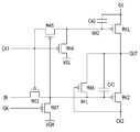
도 4는 도 3의 주사 구동 장치에 포함된 일 실시예에 따른 주사 구동 블록을 나타내는 회로도이다.4 is a circuit diagram showing a scan driving block according to an embodiment included in the scan driving device of FIG.
도 4를 참조하면, 주사 구동 블록은 복수의 트랜지스터(M11, M12, M13, M14, M15, M16, M17, M18, M19) 및 복수의 커패시터(C11, C12)를 포함한다.Referring to FIG. 4, the scan driving block includes a plurality of transistors M11, M12, M13, M14, M15, M16, M17, M18, and M19 and a plurality of capacitors C11 and C12.
제1 트랜지스터(M11)는 제2 노드(N12)에 연결되는 게이트 전극, 출력 제어신호 입력단(GK)에 연결되는 일 전극 및 출력단(OUT)에 연결되는 타 전극을 포함한다. The first transistor M11 includes a gate electrode connected to the second node N12, one electrode connected to the output control signal input terminal GK and the other electrode connected to the output terminal OUT.
제2 트랜지스터(M12)는 제1 노드(N11)에 연결되는 게이트 전극, 제3 클록 신호 입력단(CK3)에 연결되는 일 전극 및 출력단(OUT)에 연결되는 타 전극을 포함한다. The second transistor M12 includes a gate electrode connected to the first node N11, one electrode connected to the third clock signal input CK3, and another electrode connected to the output OUT.
제3 트랜지스터(M13)는 제2 클록 신호 입력단(CK2)에 연결되는 게이트 전극, 구동신호 입력단(IN)에 연결되는 일 전극 및 제1 노드(N11)에 연결되는 타 전극을 포함한다. The third transistor M13 includes a gate electrode connected to the second clock signal input CK2, a first electrode connected to the driving signal input IN and another electrode connected to the first node N11.
제4 트랜지스터(M14)는 제1 클록 신호 입력단(CK1)에 연결되는 게이트 전극, 제1 클록 신호 입력단(CK1)에 연결되는 일 전극 및 제2 노드(N12)에 연결되는 타 전극을 포함한다. The fourth transistor M14 includes a gate electrode connected to the first clock signal input terminal CK1, a first electrode connected to the first clock signal input terminal CK1, and another electrode connected to the second node N12.
제5 트랜지스터(M15)는 제2 클록 신호 입력단(CK2)에 연결되는 게이트 전극, 제1 클록 신호 입력단(CK1)에 연결되는 일 전극 및 제6 트랜지스터(M16)의 일 전극에 연결되는 타 전극을 포함한다. The fifth transistor M15 has a gate electrode connected to the second clock signal input terminal CK2, a first electrode connected to the first clock signal input terminal CK1, and another electrode connected to one electrode of the sixth transistor M16 .
제6 트랜지스터(M16)는 구동신호 입력단(IN)에 연결되는 게이트 전극, 제5 트랜지스터(M15)의 타 전극에 연결되는 일 전극 및 제2 노드(N12)에 연결되는 타 전극을 포함한다. The sixth transistor M16 includes a gate electrode connected to the driving signal input IN, a first electrode connected to the other electrode of the fifth transistor M15, and another electrode connected to the second node N12.
제7 트랜지스터(M17)는 제2 노드(N12)에 연결되는 게이트 전극, 제9 트랜지스터(M19)의 타 전극에 연결되는 일 전극 및 출력단(OUT)에 연결되는 타 전극을 포함한다. The seventh transistor M17 includes a gate electrode connected to the second node N12, one electrode connected to the other electrode of the ninth transistor M19, and another electrode connected to the output OUT.
제8 트랜지스터(M18)는 출력 제어신호 입력단(GK)에 연결되는 게이트 전극, 제1 클록 신호 입력단(CK1)에 연결되는 일 전극 및 제1 노드(N11)에 연결되는 타 전극을 포함한다. 여기서는 제8 트랜지스터(M18)의 일 전극이 제1 클록 신호 입력단(CK1)에 연결되는 것으로 나타내었으나, 제8 트랜지스터(M18)의 일 전극은 제2 클록 신호 입력단(CK2) 및 제3 클록 신호 입력단(CK3) 중 어느 하나와 연결될 수도 있다. The eighth transistor M18 includes a gate electrode connected to the output control signal input terminal GK, a first electrode connected to the first clock signal input terminal CK1, and another electrode connected to the first node N11. One electrode of the eighth transistor M18 is connected to the first clock signal input terminal CK1 while one electrode of the eighth transistor M18 is connected to the second clock signal input terminal CK2 and the third clock signal input terminal CK2. (CK3).
제9 트랜지스터(M19)는 제3 클록 신호 입력단(CK3)에 연결되는 게이트 전극, 제1 노드(N11)에 연결되는 일 전극 및 제7 트랜지스터(M17)의 일 전극에 연결되는 타 전극을 포함한다. The ninth transistor M19 includes a gate electrode connected to the third clock signal input terminal CK3, a first electrode connected to the first node N11, and another electrode connected to one electrode of the seventh transistor M17 .
제1 커패시터(C11)는 제1 노드(N11)에 연결되는 일 전극 및 출력단(OUT)에 연결되는 타 전극을 포함한다. 제2 커패시터(C12)는 출력 제어신호 입력단(GK)에 연결되는 일 전극 및 제2 노드(N12)에 연결되는 타 전극을 포함한다.The first capacitor C11 includes one electrode connected to the first node N11 and the other electrode connected to the output OUT. The second capacitor C12 includes one electrode connected to the output control signal input terminal GK and the other electrode connected to the second node N12.
복수의 트랜지스터(M11, M12, M13, M14, M15, M16, M17, M18, M19)는 p-채널 전계 효과 트랜지스터이다. 복수의 트랜지스터(M11, M12, M13, M14, M15, M16, M17, M18, M19)를 턴 온시키는 게이트 온 전압은 논리 로우 레벨의 전압이고 턴 오프시키는 게이트 오프 전압은 논리 하이 레벨의 전압이다. 여기서는 복수의 트랜지스터(M11, M12, M13, M14, M15, M16, M17, M18, M19)가 p-채널 전계 효과 트랜지스터인 것으로 설명하였으나, 복수의 트랜지스터(M11, M12, M13, M14, M15, M16, M17, M18, M19)는 n-채널 전계 효과 트랜지스터일 수 있다. n-채널 전계 효과 트랜지스터를 턴 온시키는 게이트 온 전압은 논리 하이 레벨의 전압이고 턴 오프시키는 게이트 오프 전압은 논리 로우 레벨의 전압이다. The plurality of transistors M11, M12, M13, M14, M15, M16, M17, M18, and M19 are p-channel field effect transistors. The gate-on voltage for turning on the plurality of transistors M11, M12, M13, M14, M15, M16, M17, M18 and M19 is a logic low level voltage and the gate-off voltage for turning off is a logic high level voltage. Although the plurality of transistors M11, M12, M13, M14, M15, M16, M17, M18 and M19 are described as p-channel field effect transistors, , M17, M18, M19) may be an n-channel field effect transistor. The gate on voltage that turns on the n-channel field effect transistor is a logic high level voltage and the gate off voltage that turns off is a logic low level voltage.
도 5는 도 3의 주사 구동 장치의 구동 방법을 설명하기 위한 타이밍도이다.5 is a timing chart for explaining the driving method of the scan driving device of FIG.
도 3 내지 5를 참조하면, 제안하는 주사 구동 장치는 리셋 단계(a) 및 문턱전압 보상 단계(b)에서 게이트 온 전압의 주사 신호를 복수의 주사선(S1~Sn)에 동시에 출력하고, 주사 단계(c)에서 게이트 온 전압의 주사 신호를 복수의 주사선(S1~Sn)에 순차적으로 출력한다.3 to 5, the proposed scan driving apparatus simultaneously outputs a gate-on voltage scanning signal to the plurality of scan lines S1 to Sn in the reset step (a) and the threshold voltage compensation step (b) (c) sequentially outputs the gate-on voltage scanning signal to the plurality of scanning lines S1 to Sn.
t11~t12 구간은 게이트 온 전압의 주사 신호가 복수의 주사선(S1~Sn)에 동시에 출력되는 리셋 단계(a) 및 문턱전압 보상 단계(b) 중 어느 하나의 구간을 나타낸다. t11~t12 구간에서, 출력 제어신호(GCK)는 논리 로우 레벨의 전압으로 인가되고, 주사 시작 신호(SSP), 제1 클록 신호(CLK1), 제2 클록 신호(CLK2), 제3 클록 신호(CLK3) 및 제4 클록 신호(CLK4)는 논리 하이 레벨의 전압으로 인가된다. 논리 하이 레벨의 신호에 의해 제3 트랜지스터(M13), 제4 트랜지스터(M14), 제5 트랜지스터(M15), 제6 트랜지스터(M16), 제9 트랜지스터(M19)가 턴 오프되고, 제8 트랜지스터(M18)가 턴 온된다. The period from t11 to t12 represents any one of the resetting step (a) and the threshold voltage compensating step (b) in which the scanning signal of the gate-on voltage is simultaneously outputted to the plurality of scanning lines (S1 to Sn). the output control signal GCK is applied at a logical low level and the scan start signal SSP, the first clock signal CLK1, the second clock signal CLK2, the third clock signal CLK2, CLK3 and the fourth clock signal CLK4 are applied with a logic high level voltage. The third transistor M13, the fourth transistor M14, the fifth transistor M15, the sixth transistor M16 and the ninth transistor M19 are turned off by a logic high level signal and the eighth transistor M13, M18) are turned on.
t11~t12 구간에서, 제2 커패시터(C12)의 타 전극 및 제1 트랜지스터(M11)의 게이트 전극에 연결되는 제2 노드(N12)는 플로팅 상태이다. t11 시점에서 출력 제어신호(GCK)가 논리 하이 레벨에서 논리 로우 레벨의 전압으로 낮아지면, 플로팅 상태의 제2 노드(N12)의 전압은 출력 제어신호(GCK)의 전압 변화에 따른 커플링에 의해 논리 로우 레벨로 낮아진다. 제2 노드(N12)의 전압이 논리 로우 레벨로 낮아짐에 따라 제1 트랜지스터(M11)가 턴 온된다. 제1 트랜지스터(M11)가 턴 온됨에 따라 제1 트랜지스터(M11)를 통하여 출력단(OUT)으로 논리 로우 레벨의 출력 제어신호(GCK)가 전달된다. In the interval between t11 and t12, the second node N12 connected to the other electrode of the second capacitor C12 and the gate electrode of the first transistor M11 is in a floating state. When the output control signal GCK is lowered from the logic high level to the logic low level at the time t11, the voltage of the second node N12 in the floating state is lowered by coupling according to the voltage change of the output control signal GCK Level to a logic low level. As the voltage of the second node N12 is lowered to the logic low level, the first transistor M11 is turned on. The logic low level output control signal GCK is transferred to the output terminal OUT through the first transistor M11 as the first transistor M11 is turned on.
이와 같이, 복수의 주사 구동 블록(210_1, 210_2, 210_3, 210_4, ...)은 논리 로우 레벨의 주사 신호(S[1], S[2], S[3], S[4], ...)를 동시에 출력한다. In this manner, the plurality of scan driving blocks 210_1, 210_2, 210_3, 210_4, ... are driven by the logic low level scan signals S [1], S [2], S [3], S [4] ..) at the same time.
t13 이후 구간은 게이트 온 전압의 주사 신호가 복수의 주사선(S1~Sn)에 순차적으로 출력되는 주사 단계(c)의 구간이다. t13 이후 구간에서 출력 제어신호(GCK)는 논리 하이 레벨의 전압으로 인가된다. 주사 시작 신호(SSP)는 t14~t15 구간에서 논리 로우 레벨의 전압으로 인가된다. The section after t13 is a section of the scanning step (c) in which the scanning signal of the gate-on voltage is sequentially outputted to the plurality of scanning lines S1 to Sn. In the period after t13, the output control signal GCK is applied with a logic high level voltage. The scan start signal SSP is applied at a logic low level voltage in the period from t14 to t15.
제1 클록 신호(CLK1)는 1 듀티(duty)의 논리 로우 레벨 및 대략 3 듀티의 논리 하이 레벨로 반복되는 4 듀티의 주기를 갖는다. 듀티는 주사 구동 블록에 포함되는 트랜지스터를 턴 온시키는 전압이 인가되는 구간을 의미한다. 제2 클록 신호(CLK2)는 제1 클록 신호(CLK1)가 1 듀티만큼 시프트된 신호이다. 제3 클록 신호(CLK3)는 제2 클록 신호(CLK2)가 1 듀티만큼 시프트된 신호이다. 제4 클록 신호(CLK4)는 제3 클록 신호(CLK3)가 1 듀티만큼 시프트된 신호이다. The first clock signal CLK1 has a period of a four-duty cycle which is repeated to a logic low level of one duty and a logic high level of approximately three duties. The duty is a period in which a voltage for turning on the transistors included in the scan driving block is applied. The second clock signal CLK2 is a signal in which the first clock signal CLK1 is shifted by one duty. The third clock signal CLK3 is a signal in which the second clock signal CLK2 is shifted by one duty. The fourth clock signal CLK4 is a signal in which the third clock signal CLK3 is shifted by one duty.
먼저, 첫 번째 주사 구동 블록(210_1)의 동작에 대하여 설명한다. 첫 번째 주사 구동 블록(210_1)은 4개의 클록 신호(CLK1 내지 CLK4) 중에서 제1 클록 신호(CLK1), 제2 클록 신호(CLK2) 및 제3 클록 신호(CLK3)를 이용한다. First, the operation of the first scan driving block 210_1 will be described. The first scan driving block 210_1 uses the first clock signal CLK1, the second clock signal CLK2 and the third clock signal CLK3 among the four clock signals CLK1 to CLK4.
t13~t14 구간에서, 제1 클록 신호(CLK1)가 논리 로우 레벨의 전압으로 인가되고, 나머지 클록 신호(CLK2 및 CLK3)는 논리 하이 레벨의 전압으로 인가된다. 제4 트랜지스터(M14)가 턴 온되고 논리 로우 레벨의 전압이 제2 노드(N12)에 전달된다. 제1 트랜지스터(M11)가 턴 온되고, 턴 온된 제1 트랜지스터(M11)를 통해 논리 하이 레벨의 전압이 출력단(OUT)으로 전달된다. In the period from t13 to t14, the first clock signal CLK1 is applied with a logic low level voltage and the remaining clock signals CLK2 and CLK3 are applied with a logic high level voltage. The fourth transistor M14 is turned on and the logic low level voltage is transmitted to the second node N12. The first transistor M11 is turned on and a logic high level voltage is transmitted to the output terminal OUT through the first transistor M11 turned on.
t14~t15 구간에서, 제2 클록 신호(CLK1) 및 주사 시작 신호(SSP)가 논리 로우 레벨의 전압으로 인가되고, 나머지 클록 신호(CLK1 및 CLK3)는 논리 하이 레벨의 전압으로 인가된다. 논리 로우 레벨의 신호에 의해 제3 트랜지스터(M13), 제5 트랜지스터(M15) 및 제6 트랜지스터(M16)가 턴 온된다. 제1 노드(N11)에는 논리 로우 레벨의 전압이 전달되고, 제2 노드(N12)에는 논리 하이 레벨의 전압이 전달된다. 제2 노드(N12)의 논리 하이 레벨의 전압에 의해 제1 트랜지스터(M11)가 턴 오프된다. 제1 노드(N11)의 논리 로우 레벨의 전압에 의해 제2 트랜지스터(M12)가 턴 온된다. 턴 온 된 제2 트랜지스터(M12)를 통해 논리 하이 레벨의 전압이 출력단(OUT)으로 전달된다. 이때, 제1 커패시터(C11)는 제1 노드(N11)의 논리 로우 레벨의 전압 및 출력단(OUT)의 논리 하이 레벨의 전압에 의한 전압차로 충전된다. In the period from t14 to t15, the second clock signal CLK1 and the scan start signal SSP are applied with a logic low level voltage, and the remaining clock signals CLK1 and CLK3 are applied with a logic high level voltage. The third transistor M13, the fifth transistor M15 and the sixth transistor M16 are turned on by the signal of the logic low level. A logic low level voltage is transferred to the first node N11 and a logic high level voltage is transferred to the second node N12. The first high level voltage of the second node N12 turns off the first transistor M11. The second transistor M12 is turned on by the logic low level voltage of the first node N11. A logic high level voltage is transmitted to the output terminal OUT through the turned-on second transistor M12. At this time, the first capacitor C11 is charged with the voltage difference between the logic low level voltage of the first node N11 and the logic high level voltage of the output terminal OUT.
t15~t16 구간에서, 제3 클록 신호(CLK3)가 논리 로우 레벨의 전압으로 인가되고, 나머지 클록 신호(CLK1 및 CLK2) 및 주사 시작 신호(SSP)는 논리 하이 레벨의 전압으로 인가된다. 논리 하이 레벨의 신호에 의해 제3 트랜지스터(M13), 제5 트랜지스터(M15) 및 제6 트랜지스터(M16)가 턴 오프된다. 제2 노드(N12)는 플로팅 상태가 되고, 제2 노드(N12)의 전압은 논리 하이 레벨을 유지한다. 제2 트랜지스터(M12)는 제1 커패시터(C11)를 통한 부트스트랩에 의해 완전히 턴 온된다. 턴 온된 제2 트랜지스터(M12)를 통해 논리 로우 레벨의 전압이 출력단(Out)으로 전달된다. In the interval t15 to t16, the third clock signal CLK3 is applied with a logic low level voltage and the remaining clock signals CLK1 and CLK2 and the scan start signal SSP are applied with a logic high level voltage. The third transistor M13, the fifth transistor M15 and the sixth transistor M16 are turned off by a logic high level signal. The second node N12 becomes a floating state, and the voltage of the second node N12 maintains a logic high level. The second transistor M12 is completely turned on by the bootstrap through the first capacitor C11. A logic low level voltage is transmitted to the output terminal Out via the turned-on second transistor M12.
이에 따라, 첫 번째 주사 구동 블록(210_1)은 논리 로우 레벨의 주사 신호(S[1])를 출력한다. 첫 번째 주사 구동 블록(210_1)의 논리 로우 레벨의 주사 신호(S[1])는 두 번째 주사 구동 블록(210_2)의 구동신호 입력단(IN)에 전달된다.Accordingly, the first scan driving block 210_1 outputs the scan signal S [1] of logic low level. The logic low level scan signal S [1] of the first scan driving block 210_1 is transferred to the driving signal input IN of the second scan driving block 210_2.
t16~t17 구간에서, 모든 입력 신호(CLK1, CLK2, CLK3, SSP 및 GCK)가 논리 하이 레벨의 전압으로 인가된다. 제2 트랜지스터(M13)는 제1 커패시터(C11)에 충전된 전압에 의해 턴 온된 상태를 유지하고 논리 하이 레벨의 전압이 출력단(OUT)으로 전달된다. In the interval t16 to t17, all of the input signals CLK1, CLK2, CLK3, SSP, and GCK are applied with a logic high level voltage. The second transistor M13 maintains the turned-on state by the voltage charged in the first capacitor C11 and the voltage of the logic high level is transferred to the output terminal OUT.
t17~t18 구간에서, 제1 클록 신호(CLK1)가 논리 로우 레벨의 전압으로 인가된다. 제1 클록 신호(CLK1)에 의해 제4 트랜지스터(M14)가 턴 온되고, 논리 로우 레벨의 전압이 제2 노드(N12)에 전달된다. 제2 노드(N12)의 논리 로우 레벨의 전압에 의해 제1 트랜지스터(M11)가 턴 온된다. 턴 온된 제1 트랜지스터(M11)를 통하여 논리 하이 레벨의 전압이 출력단(OUT)으로 전달된다. 이때, 제2 커패시터(C12)는 제2 노드(N12)의 논리 로우 레벨의 전압 및 출력 제어신호 입력단(GK)의 논리 하이 레벨의 전압 간의 전압차에 의해 충전된다.In the period from t17 to t18, the first clock signal CLK1 is applied at a logic low level voltage. The fourth transistor M14 is turned on by the first clock signal CLK1 and the voltage of the logic low level is transferred to the second node N12. The first transistor M11 is turned on by the logic low level voltage of the second node N12. A logic high level voltage is transmitted to the output terminal OUT through the turned-on first transistor M11. At this time, the second capacitor C12 is charged by the voltage difference between the logical low level voltage of the second node N12 and the logical high level voltage of the output control signal input terminal GK.
t18~t19 구간에서, 제2 클록 신호(CLK2)가 논리 로우 레벨의 전압으로 인가된다. 제2 클록 신호(CLK2)에 의해 제3 트랜지스터(M13) 및 제5 트랜지스터(M15)가 턴 온된다. 턴 온된 제3 트랜지스터(M13)를 통해 논리 하이 레벨의 전압이 제1 노드(N11)에 전달된다. 제1 노드(N11)의 논리 하이 레벨의 전압에 의해 제2 트랜지스터(M12)는 턴 오프된다. 제5 트랜지스터(M15)가 턴 온되더라도 제6 트랜지스터(M16)가 턴 오프 상태이므로, 제2 노드(N12)의 전압은 논리 로우 레벨의 전압을 유지한다. In the period from t18 to t19, the second clock signal CLK2 is applied with a logic low level voltage. The third transistor M13 and the fifth transistor M15 are turned on by the second clock signal CLK2. A logic high level voltage is transmitted to the first node N11 through the turned-on third transistor M13. The second transistor M12 is turned off by the logic high level voltage of the first node N11. Since the sixth transistor M16 is turned off even when the fifth transistor M15 is turned on, the voltage of the second node N12 maintains a logic low level voltage.
t19~t20 구간에서, 제3 클록 신호(CLK3)가 논리 로우 레벨의 전압으로 인가된다. 제3 클록 신호(CLK3)에 의해 제9 트랜지스터(M19)가 턴 온된다. 이때, 제2 노드(N12)는 논리 로우 레벨을 유지하고 있으므로, 제1 트랜지스터(M11) 및 제7 트랜지스터(M17)는 턴 온된 상태이다. 턴 온된 제7 트랜지스터(M11) 및 제9 트랜지스터(M19)를 통하여 출력단(OUT)으로 전달되는 논리 하이 레벨의 전압이 제1 노드(N11)에 전달된다. 제1 노드(N11)에 논리 하이 레벨의 전압이 전달됨에 따라 제3 클록 신호(CLK3)에 의해 출력단(OUT)으로 출력되는 논리 하이 레벨의 주사 신호(S[1])가 흔들리는 것을 방지한다.In the period from t19 to t20, the third clock signal CLK3 is applied as a logic low level voltage. The ninth transistor M19 is turned on by the third clock signal CLK3. At this time, since the second node N12 maintains the logic low level, the first transistor M11 and the seventh transistor M17 are turned on. A logic high level voltage which is transmitted to the output terminal OUT through the turned-on seventh transistor M11 and the ninth transistor M19 is transmitted to the first node N11. The logic high level of the scanning signal S [1] output to the output terminal OUT by the third clock signal CLK3 is prevented from shaking as the logic high level voltage is transmitted to the first node N11.
두 번째 주사 구동 블록(210_2)은 첫 번째 주사 구동 블록(210_1)이 이용하는 클록 신호(CLK1, CLK2, CLK3)보다 1 듀티 시프트된 클록 신호(CLK2, CLK3, CLK4)를 이용하므로, 두 번째 주사 구동 블록(210_2)은 첫 번째 주사 구동 블록(210_1)보다 1 듀티 만큼 늦게 논리 로우 레벨의 주사 신호(S[2])를 출력한다. 마찬가지로, 세 번째 주사 구동 블록(210_3)은 두 번째 주사 구동 블록(210_2)보다 1 듀티 만큼 늦게 논리 로우 레벨의 주사 신호(S[3])를 출력한다. 이러한 방식으로 복수의 주사 구동 블록(210_1, 210_2, 210_3, 210_4, ...)은 순차적으로 논리 로우 레벨의 주사 신호(S[1], S[2], S[3], S[4], ...)를 출력한다.The second scan driving block 210_2 uses the clock signals CLK2, CLK3 and CLK4 shifted by one duty cycle from the clock signals CLK1, CLK2 and CLK3 used by the first scan driving block 210_1, The block 210_2 outputs a logic low level scan signal S [2] later than the first scan driving block 210_1 by one duty. Similarly, the third scan driving block 210_3 outputs the logical low level scan signal S [3] later than the second scan driving block 210_2 by one duty. In this manner, the plurality of scan driving blocks 210_1, 210_2, 210_3, 210_4, ... sequentially sequentially output the logic low level scanning signals S [1], S [2], S [ , ...).
만일, 주사 구동 블록이 논리 로우 레벨의 주사 신호를 출력한 이후, 제3 클록 신호 입력단(CK3)으로 입력되는 클록 신호가 논리 로우 레벨의 전압으로 낮아질 때 제1 노드(N11)로 논리 하이 레벨의 전압이 인가되지 않는 경우, 제1 노드(N11)의 전압은 제3 클록 신호 입력단(CK3)으로 입력되는 클록 신호에 의해 흔들리게 된다. 제1 노드(N11)와 출력단(OUT)의 커플링에 의해 제1 노드(N11)의 전압이 흔들림에 따라 출력단(OUT)의 출력 신호가 흔들리게 된다.If the clock signal input to the third clock signal input terminal (CK3) is lowered to the logic low level voltage after the scan driving block outputs the logic low level scan signal, the first node (N11) When the voltage is not applied, the voltage of the first node N11 is shaken by the clock signal input to the third clock signal input terminal CK3. The output signal of the output terminal OUT fluctuates as the voltage of the first node N11 fluctuates due to coupling between the first node N11 and the output terminal OUT.
그러나, 제안하는 주사 구동 장치는 주사 구동 블록이 논리 로우 레벨의 주사 신호를 출력한 이후, 제3 클록 신호 입력단(CK3)으로 논리 로우 레벨의 클록 신호가 입력될 때 제7 트랜지스터(M17) 및 제8 트랜지스터(M18)가 턴 온되도록 하여 제1 노드(N11)로 논리 하이 레벨의 전압이 전달되도록 한다. 이에 따라, 제1 노드(N11)의 전압이 흔들리는 것을 방지할 수 있으며, 출력단(OUT)의 출력 신호가 제3 클록 신호 입력단(CK3)으로 입력되는 클록 신호에 영향을 받지 않도록 한다.However, in the proposed scan driving device, after the scan driving block outputs the logic low level scanning signal, the seventh transistor M17 and the seventh transistor M17 when the clock signal of the logic low level is input to the third clock signal input terminal CK3, 8 transistor M18 is turned on so that the logic high level voltage is transferred to the first node N11. Thus, the voltage of the first node N11 can be prevented from being shaken and the output signal of the output terminal OUT is not affected by the clock signal input to the third clock signal input terminal CK3.
뿐만 아니라, 제안하는 주사 구동 장치는 온 바이어스(on-bias) 전압이 높게 걸리는 트랜지스터가 없으며, 트랜지스터의 특성 변화에 따른 오작동을 방지할 수 있다. 또한, 제안하는 주사 구동 장치는 4개의 클록 신호(CLK1 내지 CLK4) 및 출력 제어신호(GCK)만으로 구동될 수 있으므로, 배선의 수를 줄일 수 있어 주사 구동 장치의 구조를 단순화하여 공정상이 이득을 얻을 수 있다. In addition, the proposed scan driver does not have a transistor with a high on-bias voltage and can prevent a malfunction caused by a change in the characteristics of the transistor. In addition, since the proposed scan driving device can be driven by only the four clock signals (CLK1 to CLK4) and the output control signal (GCK), the number of wirings can be reduced and the structure of the scan driving device can be simplified, .
도 6은 도 3의 주사 구동 장치에 포함된 다른 실시예에 따른 주사 구동 블록을 나타내는 회로도이다.6 is a circuit diagram showing a scan driving block according to another embodiment included in the scan driving device of FIG.
도 6를 참조하면, 주사 구동 블록은 복수의 트랜지스터(M21, M22, M23, M24, M25, M26, M27, M28, M29) 및 복수의 커패시터(C21, C22)를 포함한다.Referring to FIG. 6, the scan driving block includes a plurality of transistors M21, M22, M23, M24, M25, M26, M27, M28, and M29 and a plurality of capacitors C21 and C22.
제1 트랜지스터(M21)는 제2 노드(N22)에 연결되는 게이트 전극, 출력 제어신호 입력단(GK)에 연결되는 일 전극 및 출력단(OUT)에 연결되는 타 전극을 포함한다. The first transistor M21 includes a gate electrode connected to the second node N22, one electrode connected to the output control signal input terminal GK and the other electrode connected to the output terminal OUT.
제2 트랜지스터(M22)는 제1 노드(N21)에 연결되는 게이트 전극, 제3 클록 신호 입력단(CK3)에 연결되는 일 전극 및 출력단(OUT)에 연결되는 타 전극을 포함한다. The second transistor M22 includes a gate electrode connected to the first node N21, one electrode connected to the third clock signal input CK3, and another electrode connected to the output OUT.
제3 트랜지스터(M23)는 제2 클록 신호 입력단(CK2)에 연결되는 게이트 전극, 구동신호 입력단(IN)에 연결되는 일 전극 및 제1 노드(N21)에 연결되는 타 전극을 포함한다. The third transistor M23 includes a gate electrode connected to the second clock signal input CK2, a first electrode connected to the driving signal input IN and another electrode connected to the first node N21.
제4 트랜지스터(M24)는 제1 클록 신호 입력단(CK1)에 연결되는 게이트 전극, 제1 클록 신호 입력단(CK1)에 연결되는 일 전극 및 제2 노드(N22)에 연결되는 타 전극을 포함한다. The fourth transistor M24 includes a gate electrode connected to the first clock signal input terminal CK1, a first electrode connected to the first clock signal input terminal CK1, and another electrode connected to the second node N22.
제5 트랜지스터(M25)는 제2 클록 신호 입력단(CK2)에 연결되는 게이트 전극, 제1 클록 신호 입력단(CK1)에 연결되는 일 전극 및 제6 트랜지스터(M26)의 일 전극에 연결되는 타 전극을 포함한다. The fifth transistor M25 has a gate electrode connected to the second clock signal input CK2, a first electrode connected to the first clock signal input CK1 and another electrode connected to one electrode of the sixth transistor M26 .
제6 트랜지스터(M26)는 구동신호 입력단(IN)에 연결되는 게이트 전극, 제5 트랜지스터(M25)의 타 전극에 연결되는 일 전극 및 제2 노드(N22)에 연결되는 타 전극을 포함한다. The sixth transistor M26 includes a gate electrode connected to the driving signal input IN, a first electrode connected to the other electrode of the fifth transistor M25, and another electrode connected to the second node N22.
제7 트랜지스터(M27)는 제2 노드(N22)에 연결되는 게이트 전극, 제9 트랜지스터(M29)의 타 전극에 연결되는 일 전극 및 출력단(OUT)에 연결되는 타 전극을 포함한다. The seventh transistor M27 includes a gate electrode connected to the second node N22, one electrode connected to the other electrode of the ninth transistor M29, and another electrode connected to the output OUT.
제8 트랜지스터(M28)는 출력 제어신호 입력단(GK)에 연결되는 게이트 전극, 제1 전원전압(VGH)에 연결되는 일 전극 및 제1 노드(N21)에 연결되는 타 전극을 포함한다. 제1 전원전압(VGH)은 논리 하이 레벨의 전압을 갖는다. The eighth transistor M28 includes a gate electrode connected to the output control signal input terminal GK, a first electrode connected to the first power source voltage VGH, and another electrode connected to the first node N21. The first power supply voltage VGH has a logic high level voltage.
제9 트랜지스터(M29)는 제3 클록 신호 입력단(CK3)에 연결되는 게이트 전극, 제1 노드(N21)에 연결되는 일 전극 및 제7 트랜지스터(M27)의 일 전극에 연결되는 타 전극을 포함한다. The ninth transistor M29 includes a gate electrode connected to the third clock signal input CK3, a first electrode connected to the first node N21, and another electrode connected to one electrode of the seventh transistor M27 .
제1 커패시터(C21)는 제1 노드(N21)에 연결되는 일 전극 및 출력단(OUT)에 연결되는 타 전극을 포함한다. 제2 커패시터(C22)는 출력 제어신호 입력단(GK)에 연결되는 일 전극 및 제2 노드(N22)에 연결되는 타 전극을 포함한다.The first capacitor C21 includes one electrode connected to the first node N21 and the other electrode connected to the output OUT. The second capacitor C22 includes one electrode connected to the output control signal input terminal GK and the other electrode connected to the second node N22.
도 4의 주사 구동 블록과 비교하여, 제8 트랜지스터(M28)의 일 전극에 제1 전원전압(VGH)이 연결되는 것이 차이이다. 출력 제어신호(GCK)가 논리 로우 레벨로 인가될 때, 제8 트랜지스터(M28)를 통하여 논리 하이 레벨의 전압을 제1 노드(N21)에 전달하는 것은 도 4의 주사 구동 블록과 동일하다.Compared with the scan driving block of FIG. 4, the first power source voltage VGH is connected to one electrode of the eighth transistor M28. When the output control signal GCK is applied at the logic low level, transferring the logic high level voltage through the eighth transistor M28 to the first node N21 is the same as the scan driving block of Fig.
도 7은 도 3의 주사 구동 장치에 포함된 또 다른 실시예에 따른 주사 구동 블록을 나타내는 회로도이다.7 is a circuit diagram showing a scan driving block according to another embodiment included in the scan driving device of FIG.
도 7을 참조하면, 주사 구동 블록은 복수의 트랜지스터(M31, M32, M33, M34, M35, M36, M37, M38, M39) 및 복수의 커패시터(C31, C32)를 포함한다.Referring to FIG. 7, the scan driving block includes a plurality of transistors M31, M32, M33, M34, M35, M36, M37, M38, and M39 and a plurality of capacitors C31 and C32.
제1 트랜지스터(M31)는 제2 노드(N32)에 연결되는 게이트 전극, 출력 제어신호 입력단(GK)에 연결되는 일 전극 및 출력단(OUT)에 연결되는 타 전극을 포함한다. The first transistor M31 includes a gate electrode connected to the second node N32, one electrode connected to the output control signal input terminal GK and the other electrode connected to the output terminal OUT.
제2 트랜지스터(M32)는 제1 노드(N31)에 연결되는 게이트 전극, 제3 클록 신호 입력단(CK3)에 연결되는 일 전극 및 출력단(OUT)에 연결되는 타 전극을 포함한다. The second transistor M32 includes a gate electrode connected to the first node N31, a first electrode connected to the third clock signal input terminal CK3, and another electrode connected to the output terminal OUT.
제3 트랜지스터(M13)는 제2 클록 신호 입력단(CK2)에 연결되는 게이트 전극, 구동신호 입력단(IN)에 연결되는 일 전극 및 제1 노드(N31)에 연결되는 타 전극을 포함한다. The third transistor M13 includes a gate electrode connected to the second clock signal input CK2, a first electrode connected to the driving signal input IN and another electrode connected to the first node N31.
제4 트랜지스터(M14)는 제1 클록 신호 입력단(CK1)에 연결되는 게이트 전극, 제2 전원전압(VGL)에 연결되는 일 전극 및 제2 노드(N32)에 연결되는 타 전극을 포함한다. The fourth transistor M14 includes a gate electrode connected to the first clock signal input CK1, a first electrode connected to the second power supply voltage VGL and another electrode connected to the second node N32.
제5 트랜지스터(M35)는 제2 클록 신호 입력단(CK2)에 연결되는 게이트 전극, 제1 클록 신호 입력단(CK1)에 연결되는 일 전극 및 제6 트랜지스터(M36)의 일 전극에 연결되는 타 전극을 포함한다. The fifth transistor M35 has a gate electrode connected to the second clock signal input CK2, a first electrode connected to the first clock signal input terminal CK1, and another electrode connected to one electrode of the sixth transistor M36 .
제6 트랜지스터(M36)는 구동신호 입력단(IN)에 연결되는 게이트 전극, 제5 트랜지스터(M35)의 타 전극에 연결되는 일 전극 및 제2 노드(N32)에 연결되는 타 전극을 포함한다. The sixth transistor M36 includes a gate electrode connected to the driving signal input IN, a first electrode connected to the other electrode of the fifth transistor M35, and another electrode connected to the second node N32.
제7 트랜지스터(M37)는 제2 노드(N32)에 연결되는 게이트 전극, 제9 트랜지스터(M39)의 타 전극에 연결되는 일 전극 및 출력단(OUT)에 연결되는 타 전극을 포함한다. The seventh transistor M37 includes a gate electrode connected to the second node N32, one electrode connected to the other electrode of the ninth transistor M39, and another electrode connected to the output OUT.
제8 트랜지스터(M38)는 출력 제어신호 입력단(GK)에 연결되는 게이트 전극, 제1 클록 신호 입력단(CK1)에 연결되는 일 전극 및 제1 노드(N31)에 연결되는 타 전극을 포함한다. 여기서는 제8 트랜지스터(M38)의 일 전극이 제1 클록 신호 입력단(CK1)에 연결되는 것으로 나타내었으나, 제8 트랜지스터(M18)의 일 전극은 제2 클록 신호 입력단(CK2) 및 제3 클록 신호 입력단(CK3) 중 어느 하나와 연결될 수도 있다. The eighth transistor M38 includes a gate electrode connected to the output control signal input terminal GK, a first electrode connected to the first clock signal input terminal CK1, and another electrode connected to the first node N31. One electrode of the eighth transistor M38 is connected to the first clock signal input terminal CK1 while one electrode of the eighth transistor M18 is connected to the second clock signal input terminal CK2 and the third clock signal input terminal CK2. (CK3).
제9 트랜지스터(M39)는 제3 클록 신호 입력단(CK3)에 연결되는 게이트 전극, 제1 노드(N31)에 연결되는 일 전극 및 제7 트랜지스터(M37)의 일 전극에 연결되는 타 전극을 포함한다. The ninth transistor M39 includes a gate electrode connected to the third clock signal input CK3, a first electrode connected to the first node N31, and another electrode connected to one electrode of the seventh transistor M37 .
제1 커패시터(C31)는 제1 노드(N31)에 연결되는 일 전극 및 출력단(OUT)에 연결되는 타 전극을 포함한다. 제2 커패시터(C32)는 출력 제어신호 입력단(GK)에 연결되는 일 전극 및 제2 노드(N32)에 연결되는 타 전극을 포함한다.The first capacitor C31 includes one electrode connected to the first node N31 and the other electrode connected to the output OUT. The second capacitor C32 includes one electrode connected to the output control signal input terminal GK and the other electrode connected to the second node N32.
도 4의 주사 구동 블록과 비교하여, 제4 트랜지스터(M34)의 일 전극에 제2 전원전압(VGL)이 연결되는 것이 차이이다. 제1 클록 신호 입력단(CK1)으로 입력되는 신호가 논리 로우 레벨로 인가될 때, 제4 트랜지스터(M34)를 통하여 논리 로우 레벨의 전압을 제2 노드(N32)에 전달하는 것은 도 4의 주사 구동 블록과 동일하다.4, the second power source voltage VGL is connected to one electrode of the fourth transistor M34. When a signal input to the first clock signal input terminal CK1 is applied at a logic low level, transferring the logic low level voltage to the second node N32 through the fourth transistor M34 is equivalent to the scan driving Block.
도 8은 본 발명의 다른 실시예에 따른 주사 구동 장치의 구성을 나타내는 블록도이다. 8 is a block diagram showing a configuration of a scan driving apparatus according to another embodiment of the present invention.
도 8을 참조하면, 주사 구동 장치는 순차적으로 배열되는 복수의 주사 구동 블록(220_1, 220_2, 220_3, 220_4, ...)을 포함한다. 각 주사 구동 블록(220_1, 220_2, 220_3, 220_4, ...)은 입력 신호를 입력받아 복수의 주사선(S1~Sn) 각각에 전달되는 주사 신호(S[1], S[2], S[3], S[4], ...)를 생성한다. Referring to FIG. 8, the scan driver includes a plurality of scan driving blocks 220_1, 220_2, 220_3, 220_4,..., Sequentially arranged. Each of the scan driving blocks 220_1, 220_2, 220_3, 220_4, ... receives scan signals S [1], S [2], S [ 3], S [4], ...).
복수의 주사 구동 블록(220_1, 220_2, 220_3, 220_4, ...) 각각은 제1 클록 신호 입력단(CK1), 제2 클록 신호 입력단(CK2), 출력 제어신호 입력단(GK), 구동신호 입력단(IN) 및 출력단(OUT)을 포함한다. Each of the plurality of scan driving blocks 220_1, 220_2, 220_3, 220_4, ... has a first clock signal input terminal CK1, a second clock signal input terminal CK2, an output control signal input terminal GK, IN and an output terminal OUT.
복수의 주사 구동 블록(220_1, 220_2, 220_3, 220_4, ...) 중 홀수 번째 주사 구동 블록(220_1, 220_3, ...)의 제1 클록 신호 입력단(CK1)에는 제1 클록 신호(CLK1)가 입력되고, 제2 클록 신호 입력단(CK2)에는 제2 클록 신호(CLK2)가 입력된다. 그리고 복수의 주사 구동 블록(220_1, 220_2, 220_3, 220_4, ...) 중 짝수 번째 주사 구동 블록(220_2, 220_4, ...)의 제1 클록 신호 입력단(CK1)에는 제2 클록 신호(CLK2)가 입력되고, 제2 클록 신호 입력단(CK2)에는 제1 클록 신호(CLK1)가 입력된다.The first clock signal CLK1 is input to the first clock signal input terminal CK1 of the odd-numbered scan driving blocks 220_1, 220_3, ... among the plurality of scan driving blocks 220_1, 220_2, 220_3, 220_4, And the second clock signal CLK2 is input to the second clock signal input terminal CK2. The second clock signal CLK2 is input to the first clock signal input terminal CK1 of the even-numbered scan driving blocks 220_2, 220_4, ... among the plurality of scan driving blocks 220_1, 220_2, 220_3, 220_4, And the first clock signal CLK1 is input to the second clock signal input terminal CK2.
복수의 주사 구동 블록(220_1, 220_2, 220_3, 220_4, ...)의 출력 제어신호 입력단(GK)에는 출력 제어신호(GCK)가 입력된다.An output control signal GCK is input to the output control signal input terminals GK of the plurality of scan driving blocks 220_1, 220_2, 220_3, 220_4,.
복수의 주사 구동 블록(220_1, 220_2, 220_3, 220_4, ...)의 구동신호 입력단(IN)에는 앞서 배열된 주사 구동 블록의 주사 신호가 입력된다. 즉, 홀수 번째 주사 구동 블록의 구동 신호 입력단(IN)에는 앞서 배열된 짝수 번째 주사 구동 블록의 주사 신호가 입력된다. 짝수 번째 주사 구동 블록의 구동 신호 입력단(IN)에는 앞서 배열된 홀수 번째 주사 구동 블록의 주사 신호가 입력된다.The scan signals of the scan driving blocks arranged in advance are inputted to the drive signal input terminals IN of the plurality of scan drive blocks 220_1, 220_2, 220_3, 220_4,. That is, the scan signals of the even-numbered scan driving blocks arranged in the preceding stage are input to the drive signal input terminals IN of the odd-numbered scan drive blocks. Numbered scanning driving blocks IN are input to the driving signal input IN of the even-numbered scanning driving blocks.
다시 말해, 복수의 주사 구동 블록(220_1, 220_2, 220_3, 220_4, ...)이 순차적으로 주사 신호를 출력할 때, k번째 주사 구동 블록(220_k)의 구동신호 입력단(IN)에는 k-1번째 주사 구동 블록(220_k-1)의 주사 신호(S[k-1])가 입력된다. 이때, 첫 번째 주사 구동 블록(220_1)의 구동신호 입력단(IN)에는 주사 시작 신호(SSP)가 입력된다.In other words, when a plurality of scan driving blocks 220_1, 220_2, 220_3, 220_4, ... sequentially output scan signals, a drive signal input IN of the kth scan drive block 220_k is supplied with k-1 Th scan driving block 220_k-1 is input to the scan driver circuit 220_k-1. At this time, the scan start signal SSP is input to the drive signal input IN of the first scan driving block 220_1.
각 주사 구동 블록(220_1, 220_2, 220_3, 220_4, ...)은 제1 클록 신호 입력단(CK1), 제2 클록 신호 입력단(CK2), 출력 제어신호 입력단(GK) 및 구동신호 입력단(IN)으로 입력되는 신호에 따라 생성된 주사 신호(S[1], S[2], S[3], S[4], ...)를 출력단(OUT)으로 출력한다.Each of the scan driving blocks 220_1, 220_2, 220_3, 220_4, ... has a first clock signal input terminal CK1, a second clock signal input terminal CK2, an output control signal input terminal GK, And outputs the generated scanning signals S [1], S [2], S [3], S [4], ... according to a signal input to the output terminal OUT.
첫 번째 주사 구동 블록(220_1)은 주사 시작 신호(SSP)를 입력받아 생성한 주사 신호(S[1])를 첫 번째 주사선(S1) 및 두 번째 주사 구동 블록(220_2)의 구동신호 입력단(IN)에 전달한다. k 번째 배열된 주사 구동 블록(220_k)은 k-1 번째 배열된 주사 구동 블록(220_k-1)에서 출력되는 주사 신호(S[k-1])를 입력받아 생성된 주사 신호(S[k])를 출력한다(1<k<=n).The first scan driving block 220_1 receives the scan signal S [1] generated by receiving the scan start signal SSP as the first scan line S1 and the drive signal input IN of the second scan driving block 220_2 ). The k-th arranged scan driving block 220_k receives the scan signal S [k] generated by receiving the scan signal S [k-1] output from the k-1th arranged scan driving block 220_k- ) (1 < k < = n).
도 9는 도 8의 주사 구동 장치에 포함된 일 실시예에 따른 주사 구동 블록을 나타내는 회로도이다.9 is a circuit diagram showing a scan driving block according to an embodiment included in the scan driving device of FIG.
도 9를 참조하면, 주사 구동 블록은 복수의 트랜지스터(M41, M42, M43, M44, M45, M46, M47) 및 복수의 커패시터(C41, C42)를 포함한다.Referring to FIG. 9, the scan driving block includes a plurality of transistors M41, M42, M43, M44, M45, M46, and M47 and a plurality of capacitors C41 and C42.
제1 트랜지스터(M41)는 제2 노드(N42)에 연결되는 게이트 전극, 출력 제어신호 입력단(GK)에 연결되는 일 전극 및 출력단(OUT)에 연결되는 타 전극을 포함한다. The first transistor M41 includes a gate electrode connected to the second node N42, one electrode connected to the output control signal input terminal GK and the other electrode connected to the output terminal OUT.
제2 트랜지스터(M42)는 제1 노드(N41)에 연결되는 게이트 전극, 제2 클록 신호 입력단(CK2)에 연결되는 일 전극 및 출력단(OUT)에 연결되는 타 전극을 포함한다. The second transistor M42 includes a gate electrode connected to the first node N41, a first electrode connected to the second clock signal input terminal CK2, and another electrode connected to the output terminal OUT.
제3 트랜지스터(M43)는 제1 클록 신호 입력단(CK1)에 연결되는 게이트 전극, 구동신호 입력단(IN)에 연결되는 일 전극 및 제1 노드(N41)에 연결되는 타 전극을 포함한다. The third transistor M43 includes a gate electrode connected to the first clock signal input CK1, a first electrode connected to the driving signal input IN, and another electrode connected to the first node N41.
제4 트랜지스터(M44)는 제1 클록 신호 입력단(CK1)에 연결되는 게이트 전극, 제2 전원 전압(VGL)에 연결되는 일 전극 및 제2 노드(N42)에 연결되는 타 전극을 포함한다. The fourth transistor M44 includes a gate electrode connected to the first clock signal input terminal CK1, a first electrode connected to the second power source voltage VGL and another electrode connected to the second node N42.
제5 트랜지스터(M45)는 제1 노드(N41)에 연결되는 게이트 전극, 제1 클록 신호 입력단(CK1)에 연결되는 일 전극 및 제2 노드(N42)에 연결되는 타 전극을 포함한다. The fifth transistor M45 includes a gate electrode connected to the first node N41, a first electrode connected to the first clock signal input terminal CK1, and another electrode connected to the second node N42.
제6 트랜지스터(M46)는 제2 클록 신호 입력단(CK2)에 연결되는 게이트 전극, 제1 노드(N41)에 연결되는 일 전극 및 출력단(OUT)에 연결되는 타 전극을 포함한다.The sixth transistor M46 includes a gate electrode connected to the second clock signal input CK2, a first electrode connected to the first node N41, and another electrode connected to the output OUT.
제7 트랜지스터(M47)는 출력 제어신호 입력단(GK)에 연결되는 게이트 전극, 제1 전원 전압(VGH)에 연결되는 일 전극 및 제1 노드(N41)에 연결되는 타 전극을 포함한다. The seventh transistor M47 includes a gate electrode connected to the output control signal input terminal GK, a first electrode connected to the first power source voltage VGH, and another electrode connected to the first node N41.
제1 커패시터(C41)는 제1 노드(N41)에 연결되는 일 전극 및 출력단(OUT)에 연결되는 타 전극을 포함한다. 제2 커패시터(C42)는 출력 제어신호 입력단(GK)에 연결되는 일 전극 및 제2 노드(N42)에 연결되는 타 전극을 포함한다.The first capacitor C41 includes one electrode connected to the first node N41 and the other electrode connected to the output OUT. The second capacitor C42 includes one electrode connected to the output control signal input terminal GK and the other electrode connected to the second node N42.
복수의 트랜지스터(M41, M42, M43, M44, M45, M46, M47)는 p-채널 전계 효과 트랜지스터이다. 복수의 트랜지스터(M41, M42, M43, M44, M45, M46, M47)를 턴 온시키는 게이트 온 전압은 논리 로우 레벨의 전압이고 턴 오프시키는 게이트 오프 전압은 논리 하이 레벨의 전압이다. 여기서는 복수의 트랜지스터(M41, M42, M43, M44, M45, M46, M47)가 p-채널 전계 효과 트랜지스터인 것으로 설명하였으나, 복수의 트랜지스터(M41, M42, M43, M44, M45, M46, M47)는 n-채널 전계 효과 트랜지스터일 수 있다. n-채널 전계 효과 트랜지스터를 턴 온시키는 게이트 온 전압은 논리 하이 레벨의 전압이고 턴 오프시키는 게이트 오프 전압은 논리 로우 레벨의 전압이다. The plurality of transistors M41, M42, M43, M44, M45, M46, and M47 are p-channel field effect transistors. The gate-on voltage for turning on the plurality of transistors M41, M42, M43, M44, M45, M46, and M47 is a logic low level voltage and the gate-off voltage for turning off is a logic high level voltage. Although the plurality of transistors M41, M42, M43, M44, M45, M46 and M47 are described as p-channel field effect transistors, channel field-effect transistor. The gate on voltage that turns on the n-channel field effect transistor is a logic high level voltage and the gate off voltage that turns off is a logic low level voltage.
도 10은 도 8의 주사 구동 장치의 구동 방법을 설명하기 위한 타이밍도이다.10 is a timing chart for explaining the driving method of the scan driving apparatus of FIG.
도 8 내지 10을 참조하면, 제안하는 주사 구동 장치는 리셋 단계(a) 및 문턱전압 보상 단계(b)에서 게이트 온 전압의 주사 신호를 복수의 주사선(S1~Sn)에 동시에 출력하고, 주사 단계(c)에서 게이트 온 전압의 주사 신호를 복수의 주사선(S1~Sn)에 순차적으로 출력한다.Referring to Figs. 8 to 10, the proposed scan driving apparatus simultaneously outputs a gate-on voltage scanning signal to the plurality of scan lines S1 to Sn in the reset step (a) and the threshold voltage compensating step (b) (c) sequentially outputs the gate-on voltage scanning signal to the plurality of scanning lines S1 to Sn.
t21~t22 구간은 게이트 온 전압의 주사 신호가 복수의 주사선(S1~Sn)에 동시에 출력되는 리셋 단계(a) 및 문턱전압 보상 단계(b) 중 어느 하나의 구간을 나타낸다. t21~t22 구간에서, 출력 제어신호(GCK)는 논리 로우 레벨의 전압으로 인가되고, 주사 시작 신호(SSP), 제1 클록 신호(CLK1) 및 제2 클록 신호(CLK2)는 논리 하이 레벨의 전압으로 인가된다. 논리 하이 레벨의 신호에 의해 제3 트랜지스터(M43), 제4 트랜지스터(M44), 제6 트랜지스터(M46)가 턴 오프된다. 출력 제어신호(GCK)에 의해 제7 트랜지스터(M47)가 턴 온된다. 턴 온된 제7 트랜지스터(M47)를 통해 제1 전원 전압(VGH)이 제5 트랜지스터(M45)에 전달되어, 제5 트랜지스터(M45)가 턴 오프된다.The section from t21 to t22 represents any one of the resetting step (a) and the threshold voltage compensating step (b) in which the scanning signal of the gate-on voltage is simultaneously outputted to the plurality of scanning lines (S1 to Sn). the output control signal GCK is applied at a logic low level voltage and the scan start signal SSP, the first clock signal CLK1 and the second clock signal CLK2 are at a logical high level voltage . The third transistor M43, the fourth transistor M44 and the sixth transistor M46 are turned off by a logic high level signal. The seventh transistor M47 is turned on by the output control signal GCK. The first power source voltage VGH is transmitted to the fifth transistor M45 through the turned-on seventh transistor M47 so that the fifth transistor M45 is turned off.
t21~t22 구간에서, 제2 커패시터(C42)의 타 전극 및 제1 트랜지스터(M41)의 게이트 전극에 연결되는 제2 노드(N42)는 플로팅 상태이다. t21 시점에서 출력 제어신호(GCK)가 논리 하이 레벨에서 논리 로우 레벨의 전압으로 낮아지면, 플로팅 상태의 제2 노드(N42)의 전압은 출력 제어신호(GCK)의 전압 변화에 따른 커플링에 의해 논리 로우 레벨로 낮아진다. 제2 노드(N42)의 전압이 논리 로우 레벨로 낮아짐에 따라 제1 트랜지스터(M41)가 턴 온된다. 제1 트랜지스터(M41)가 턴 온됨에 따라 제1 트랜지스터(M41)를 통하여 출력단(OUT)으로 논리 로우 레벨의 출력 제어신호(GCK)가 전달된다. The second node N42 connected to the other electrode of the second capacitor C42 and the gate electrode of the first transistor M41 in the period from t21 to t22 is in a floating state. When the output control signal GCK is lowered from the logic high level to the logic low level at time t21, the voltage of the second node N42 in the floating state is lowered by coupling according to the voltage change of the output control signal GCK Level to a logic low level. As the voltage of the second node N42 is lowered to a logic low level, the first transistor M41 is turned on. The logic low level output control signal GCK is transferred to the output terminal OUT through the first transistor M41 as the first transistor M41 is turned on.
이와 같이, 복수의 주사 구동 블록(220_1, 220_2, 220_3, 220_4, ...)은 논리 로우 레벨의 주사 신호(S[1], S[2], S[3], S[4], ...)를 동시에 출력한다.As described above, the plurality of scan driving blocks 220_1, 220_2, 220_3, 220_4, ... are driven by the logic low level scan signals S [1], S [2], S [3], S [4],. ..) at the same time.
t23 이후 구간은 게이트 온 전압의 주사 신호가 복수의 주사선(S1~Sn)에 순차적으로 출력되는 주사 단계(c)의 구간이다. t23 이후 구간에서 출력 제어신호(GCK)는 논리 하이 레벨의 전압으로 인가된다.The section after t23 is a section of the scanning step (c) in which the scanning signal of the gate-on voltage is sequentially outputted to the plurality of scanning lines S1 to Sn. In the period after t23, the output control signal GCK is applied with a logic high level voltage.
주사 시작 신호(SSP)는 t23~t24 구간에서 논리 로우 레벨의 전압으로 인가된다. 제1 클록 신호(CLK1)의 전압은 t23~t24 구간부터 논리 로우 레벨 및 논리 하이 레벨로 반복하여 바뀐다. 제2 클록 신호(CLK2)의 전압은 t24~t25 구간부터 논리 로우 레벨 및 논리 하이 레벨로 반복하여 바뀐다. 즉, 제2 클록 신호(CLK2)는 제1 클록 신호(CLK1)가 제1 주사 신호(CLK1)의 듀티(duty)만큼 시프트된 신호이다. 클록 신호의 듀티는 주사 구동 블록에 포함되는 트랜지스터를 턴 온시키는 전압이 인가되는 구간을 의미한다.The scan start signal SSP is applied at a logic low level voltage in the interval t23 to t24. The voltage of the first clock signal CLK1 is repeatedly changed from the t23 to t24 period to the logic low level and the logic high level. The voltage of the second clock signal CLK2 is repeatedly changed from the t24 to t25 period to the logic low level and the logic high level. That is, the second clock signal CLK2 is a signal in which the first clock signal CLK1 is shifted by the duty of the first scan signal CLK1. The duty of the clock signal means a period in which a voltage for turning on the transistors included in the scan driving block is applied.
t23~t24 구간에서, 첫 번째 주사 구동 블록(220_1)의 구동신호 입력단(IN)에 논리 로우 레벨의 주사 시작 신호(SSP)가 인가되고, 제1 클록 신호 입력단(CK1)에 논리 로우 레벨의 제1 클록 신호(CLK1)가 인가된다. 제3 트랜지스터(M43) 및 제4 트랜지스터(M44)가 턴 온된다. 제1 노드(N41)에는 논리 로우 레벨의 주사 시작 신호(SSP)가 전달되고, 제2 노드(N42)에는 제2 전원 전압(VGL)이 전달된다. 제1 트랜지스터(M41) 및 제2 트랜지스터(M42)가 턴 온 된다. 출력단(OUT)으로 논리 하이 레벨의 전압이 전달된다. 이때, 제1 커패시터(C41)는 제1 노드(N41)의 논리 로우 레벨의 전압 및 출력단(OUT)의 논리 하이 레벨의 전압에 의한 전압차로 충전된다.a logic low level scan start signal SSP is applied to the drive signal input IN of the first scan driving block 220_1 in the interval t23 to t24 and a logic low level scan start signal SSP is applied to the first clock signal input CK1. 1 clock signal CLK1 is applied. The third transistor M43 and the fourth transistor M44 are turned on. A logic low level scan start signal SSP is transferred to the first node N41 and a second power source voltage VGL is transferred to the second node N42. The first transistor M41 and the second transistor M42 are turned on. And a logic high level voltage is transmitted to the output terminal OUT. At this time, the first capacitor C41 is charged with the voltage difference between the logical low level voltage of the first node N41 and the logic high level voltage of the output terminal OUT.
t24~t25 구간에서, 첫 번째 주사 구동 블록(220_1)의 제1 클록 신호 입력단(CK1)에는 논리 하이 레벨의 제1 클록 신호(CLK1)가 인가되고, 제2 클록 신호 입력단(CK2)에는 논리 로우 레벨의 제2 클록 신호(CLK2)가 인가된다. 제3 트랜지스터(M43) 및 제4 트랜지스터(M44)가 턴 오프되고, 제6 트랜지스터(M46)가 턴 온된다. 제2 트랜지스터(M42)는 제1 커패시터(C41)를 통한 부트스트랩에 의해 완전히 턴 온된다. 턴 온된 제2 트랜지스터(M42)를 통해 논리 로우 레벨의 전압이 출력단(OUT)으로 전달된다. 이때, 제1 노드(N41)의 전압은 커플링에 의해 논리 로우 레벨의 전압으로 낮아진다. 제1 노드(N41)의 논리 로우 레벨의 전압에 의해 제5 트랜지스터(M45)가 턴 온되고, 논리 하이 레벨의 전압이 제2 노드(N42)에 전달된다. 제2 노드(N42)의 논리 하이 레벨의 전압에 의해 제1 트랜지스터(M41)는 턴 오프된다.a logic high level first clock signal CLK1 is applied to the first clock signal input terminal CK1 of the first scan driving block 220_1 and a logic low level signal is input to the second clock signal input terminal CK2 in the interval t24 to t25. Level second clock signal CLK2 is applied. The third transistor M43 and the fourth transistor M44 are turned off and the sixth transistor M46 is turned on. The second transistor M42 is completely turned on by the bootstrap through the first capacitor C41. A logic low level voltage is transmitted to the output terminal OUT through the turned-on second transistor M42. At this time, the voltage of the first node N41 is lowered to a logic low level voltage by coupling. The fifth transistor M45 is turned on by the logic low level voltage of the first node N41 and the logic high level voltage is transmitted to the second node N42. The first transistor M41 is turned off by the logic high level voltage of the second node N42.
이에 따라, 첫 번째 주사 구동 블록(220_1)은 논리 로우 레벨의 주사 신호(S[1])를 출력한다. Accordingly, the first scan driving block 220_1 outputs the scan signal S [1] of logic low level.
t24~t25 구간에서, 첫 번째 주사 구동 블록(220_1)의 논리 로우 레벨의 주사 신호(S[1])는 두 번째 주사 구동 블록(220_2)의 구동신호 입력단(IN)에 인가된다. 두 번째 주사 구동 블록(220_2)의 제1 클록 신호 입력단(CK1)에는 논리 로우 레벨의 제2 클록 신호(CLK2)가 인가되고, 제2 클록 신호 입력단(CK2)에는 논리 하이 레벨의 제1 클록 신호(CLK1)가 인가된다. 두 번째 주사 구동 블록(220_2)은 첫 번째 주사 구동 블록(220_1)의 t23~t24 구간에서의 동작과 동일하게 동작하여 제1 커패시터(C41)를 제1 노드(N41)의 논리 로우 레벨의 전압 및 출력단(OUT)의 논리 하이 레벨의 전압에 의한 전압차로 충전시킨다. the logic low level scan signal S [1] of the first scan driving block 220_1 is applied to the drive signal input IN of the second scan driving block 220_2 in the interval t24 to t25. A logic low level second clock signal CLK2 is applied to the first clock signal input terminal CK1 of the second scan driving block 220_2 and a first clock signal CLK2 of logic high level is applied to the second clock signal input terminal CK2, (CLK1) is applied. The second scan driving block 220_2 operates in the same manner as the operation in the interval t23 to t24 of the first scan driving block 220_1 so that the first capacitor C41 is connected to the logical low level voltage of the first node N41, And is charged with a voltage difference caused by a logic high level voltage at the output terminal OUT.
t25~t26 구간에서, 두 번째 주사 구동 블록(220_2)의 제1 클록 신호 입력단(CK1)에는 논리 하이 레벨의 제2 클록 신호(CLK2)가 인가되고, 제2 클록 신호 입력단(CK2)에는 논리 로우 레벨의 제1 클록 신호(CLK1)가 인가된다. 두 번째 주사 구동 블록(220_2)은 첫 번째 주사 구동 블록(220_1)의 t24~t25 구간에서의 동작과 동일하게 동작하여 논리 로우 레벨의 주사 신호(S[2])를 출력한다. a logic high level second clock signal CLK2 is applied to the first clock signal input terminal CK1 of the second scan driving block 220_2 in the interval t25 to t26, Level first clock signal CLK1 is applied. The second scan driving block 220_2 operates in the same manner as the operation in the interval t24 to t25 of the first scan driving block 220_1 to output the logical low level scan signal S [2].
t25~t26 구간에서, 첫 번째 주사 구동 블록(220_1)의 제1 클록 신호 입력단(CK1)에는 논리 로우 레벨의 제1 클록 신호(CLK1)가 입력되고, 제2 클록 신호 입력단(CK2)에는 논리 하이 레벨의 제2 클록 신호(CLK2)가 입력된다. 제3 트랜지스터(M43) 및 제4 트랜지스터(M44)가 턴 온된다. 제1 노드(N41)에는 논리 하이 레벨의 전압이 전달되고, 제2 노드(N42)에 제2 전원 전압(VGL)이 전달된다. 제1 노드(N41)의 논리 하이 레벨의 전압에 의해 제2 트랜지스터(M42)는 턴 오프된다. 제2 노드(N42)의 논리 로우 레벨의 전압에 의해 제1 트랜지스터(M41)가 턴 온되고, 출력단(OUT)으로 논리 하이 레벨의 전압이 전달된다. 이때, 제2 커패시터(C42)는 제2 노드(N42)의 논리 로우 레벨의 전압 및 출력 제어 신호 입력단(GK)의 논리 하이 레벨의 전압에 의한 전압차로 충전된다.the logic low level first clock signal CLK1 is input to the first clock signal input terminal CK1 of the first scan driving block 220_1 and the logic high level input terminal CK2 is input to the second clock signal input terminal CK2 in the interval t25 to t26. Level second clock signal CLK2. The third transistor M43 and the fourth transistor M44 are turned on. A logic high level voltage is transferred to the first node N41 and a second power source voltage VGL is transferred to the second node N42. The second transistor M42 is turned off by the logic high level voltage of the first node N41. The first transistor M41 is turned on by the logic low level voltage of the second node N42 and the logic high level voltage is transferred to the output terminal OUT. At this time, the second capacitor C42 is charged with the voltage difference between the logical low level voltage of the second node N42 and the logic high level voltage of the output control signal input terminal GK.
t26~t27 구간에서, 첫 번째 주사 구동 블록(220_1)의 제1 클록 신호 입력단(CK1)에는 논리 하이 레벨의 제1 클록 신호(CLK1)가 입력되고, 제2 클록 신호 입력단(CK2)에는 논리 로우 레벨의 제2 클록 신호(CLK2)가 입력된다. 제3 트랜지스터(M43) 및 제4 트랜지스터(M44)가 턴 오프된다. 제1 트랜지스터(M41)는 제2 커패시터(C42)에 충전된 전압에 의해 턴 온 상태를 유지하고, 출력단(OUT)으로 논리 하이 레벨의 출력 제어 신호(GCK)를 전달한다. 논리 로우 레벨의 제2 클록 신호(CLK2)에 의해 제6 트랜지스터(M46)가 턴 온되고, 제1 노드(N41)에는 출력단(OUT)의 논리 하이 레벨의 전압이 전달된다. 제1 노드(N41)의 논리 하이 레벨의 전압에 의해 제2 트랜지스터(M42)는 턴 오프된 상태를 유지한다.the logic high level first clock signal CLK1 is input to the first clock signal input terminal CK1 of the first scan driving block 220_1 and the logic low input terminal CK2 is input to the second clock signal input terminal CK2 in the interval t26 to t27. Level second clock signal CLK2. The third transistor M43 and the fourth transistor M44 are turned off. The first transistor M41 maintains the turn-on state by the voltage charged in the second capacitor C42 and delivers a logic high level output control signal GCK to the output OUT. The sixth transistor M46 is turned on by the second clock signal CLK2 of the logic low level and the logic high level voltage of the output terminal OUT is transferred to the first node N41. The second transistor M42 is kept turned off by the logic high level voltage of the first node N41.
이와 같이, 논리 로우 레벨의 주사 신호를 출력한 후 제1 클록 신호 입력단(CK1)에 입력되는 클록 신호 및 제2 클록 신호 입력단(CK2)에 입력되는 클록 신호에 따라 제1 노드(N41)에 논리 하이 레벨의 전압을 전달함으로써, 첫 번째 주사 구동 블록(220_1)의 주사 신호(S[1])가 제2 클록 신호 입력단(CK2)으로 인가되는 클록 신호에 의해 흔들리지 않도록 한다.After the logic low level scan signal is output, the first node N41 is driven in accordance with the clock signal input to the first clock signal input terminal (CK1) and the clock signal input to the second clock signal input terminal (CK2) The scan signal S [1] of the first scan driving block 220_1 is not shaken by the clock signal applied to the second clock signal input terminal CK2 by transmitting a high level voltage.
상술한 방식으로, 복수의 주사 구동 블록(220_1, 220_2, 220_3, 220_4, ...)은 순차적으로 논리 로우 레벨의 주사 신호(S[1], S[2], S[3], S[4], ...)를 출력한다.In the above-described manner, the plurality of scan driving blocks 220_1, 220_2, 220_3, 220_4, ... sequentially output the logic low level scan signals S [1], S [ 4], ...).
만일, 주사 구동 블록이 논리 로우 레벨의 주사 신호를 출력한 후, 제1 노드(N41)로 논리 하이 레벨의 전압이 전달되지 않으면, 제2 클록 신호 입력단(CK2)으로 입력되는 클록 신호의 전압 변동에 의해 제1 노드(N41)의 전압이 흔들리게 된다. 제1 노드(N41)와 출력단(OUT)의 커플링에 의해 제1 노드(N41)의 전압이 흔들림에 따라 출력단(OUT)의 출력 신호가 흔들리게 된다.If the logical high level voltage is not transferred to the first node N41 after the scan driving block outputs the logical low level scan signal, the voltage fluctuation of the clock signal input to the second clock signal input terminal (CK2) The voltage of the first node N41 is shaken. The output signal of the output terminal OUT fluctuates as the voltage of the first node N41 fluctuates due to coupling between the first node N41 and the output terminal OUT.
그러나, 제안하는 주사 구동 장치는 주사 구동 블록이 논리 로우 레벨의 주사 신호를 출력한 이후, 제1 클록 신호 입력단(CLK1)에 입력되는 클록 신호 및 제2 클록 신호 입력단(CK2)에 입력되는 클록 신호에 따라 제1 노드(N41)에 논리 하이 레벨의 전압을 전달함으로써 주사 구동 블록의 출력 신호가 흔들리는 것을 방지하고, 출력단(OUT)의 출력 신호가 제2 클록 신호 입력단(CK2)으로 입력되는 클록 신호에 영향을 받지 않도록 한다.However, in the proposed scan driving apparatus, after the scan driving block outputs the logic low level scanning signal, the clock signal input to the first clock signal input terminal (CLK1) and the clock signal input to the second clock signal input terminal (CK2) By preventing the output signal of the scan driving block from being shaken by transmitting a logic high level voltage to the first node N41 according to the clock signal CK2 inputted to the first node N41, .
뿐만 아니라, 제안하는 주사 구동 장치는 제안하는 주사 구동 장치는 2개의 클록 신호(CLK1, CLK2), 출력 제어신호(GCK) 및 2개의 전원만으로 구동될 수 있으므로, 배선의 수를 줄일 수 있어 주사 구동 장치의 구조를 단순화하여 공정상이 이득을 얻을 수 있다. In addition, since the proposed scan driving device can be driven by only two power sources and two clock signals (CLK1 and CLK2) and an output control signal (GCK), the number of wirings can be reduced, The structure of the apparatus can be simplified and a gain in the process can be obtained.
도 11은 도 8의 주사 구동 장치에 포함된 다른 실시예에 따른 주사 구동 블록을 나타내는 회로도이다.11 is a circuit diagram showing a scan driving block according to another embodiment included in the scan driving device of FIG.
도 11을 참조하면, 주사 구동 블록은 복수의 트랜지스터(M51, M52, M53, M54, M55, M56, M57) 및 복수의 커패시터(C51, C52)를 포함한다.Referring to FIG. 11, the scan driving block includes a plurality of transistors M51, M52, M53, M54, M55, M56 and M57 and a plurality of capacitors C51 and C52.
제1 트랜지스터(M51)는 제2 노드(N52)에 연결되는 게이트 전극, 출력 제어신호 입력단(GK)에 연결되는 일 전극 및 출력단(OUT)에 연결되는 타 전극을 포함한다. The first transistor M51 includes a gate electrode connected to the second node N52, one electrode connected to the output control signal input terminal GK and the other electrode connected to the output terminal OUT.
제2 트랜지스터(M52)는 제1 노드(N51)에 연결되는 게이트 전극, 제2 클록 신호 입력단(CK2)에 연결되는 일 전극 및 출력단(OUT)에 연결되는 타 전극을 포함한다. The second transistor M52 includes a gate electrode connected to the first node N51, a first electrode connected to the second clock signal input CK2, and another electrode connected to the output OUT.
제3 트랜지스터(M53)는 구동신호 입력단(IN)에 연결되는 게이트 전극, 구동신호 입력단(IN)에 연결되는 일 전극 및 제1 노드(N51)에 연결되는 타 전극을 포함한다.The third transistor M53 includes a gate electrode connected to the driving signal input IN, one electrode connected to the driving signal input IN and another electrode connected to the first node N51.
제4 트랜지스터(M54)는 제1 클록 신호 입력단(CK1)에 연결되는 게이트 전극, 제2 전원 전압(VGL)에 연결되는 일 전극 및 제2 노드(N52)에 연결되는 타 전극을 포함한다. The fourth transistor M54 includes a gate electrode connected to the first clock signal input terminal CK1, a first electrode connected to the second power supply voltage VGL, and another electrode connected to the second node N52.
제5 트랜지스터(M55)는 제1 노드(N51)에 연결되는 게이트 전극, 제1 클록 신호 입력단(CK1)에 연결되는 일 전극 및 제2 노드(N52)에 연결되는 타 전극을 포함한다. The fifth transistor M55 includes a gate electrode connected to the first node N51, a first electrode connected to the first clock signal input terminal CK1, and another electrode connected to the second node N52.
제6 트랜지스터(M56)는 제2 클록 신호 입력단(CK2)에 연결되는 게이트 전극, 제1 노드(N51)에 연결되는 일 전극 및 출력단(OUT)에 연결되는 타 전극을 포함한다.The sixth transistor M56 includes a gate electrode connected to the second clock signal input CK2, a first electrode connected to the first node N51 and another electrode connected to the output OUT.
제7 트랜지스터(M57)는 출력 제어신호 입력단(GK)에 연결되는 게이트 전극, 제1 전원 전압(VGH)에 연결되는 일 전극 및 제1 노드(N51)에 연결되는 타 전극을 포함한다.The seventh transistor M57 includes a gate electrode connected to the output control signal input terminal GK, a first electrode connected to the first power source voltage VGH, and another electrode connected to the first node N51.
제1 커패시터(C51)는 제1 노드(N51)에 연결되는 일 전극 및 출력단(OUT)에 연결되는 타 전극을 포함한다. 제2 커패시터(C52)는 출력 제어신호 입력단(GK)에 연결되는 일 전극 및 제2 노드(N52)에 연결되는 타 전극을 포함한다.The first capacitor C51 includes one electrode connected to the first node N51 and the other electrode connected to the output OUT. The second capacitor C52 includes one electrode connected to the output control signal input terminal GK and the other electrode connected to the second node N52.
도 9의 주사 구동 블록과 비교하여, 제3 트랜지스터(M53)의 게이트 전극이 구동신호 입력단(IN)에 연결되는 것이 차이이다. 구동신호 입력단(IN)으로 논리 로우 레벨의 주사 시작 신호(SSP) 또는 주사 신호가 인가될 때, 제3 트랜지스터(M53)를 통하여 논리 로우 레벨의 전압을 제1 노드(N51)에 전달하는 것은 도 9의 주사 구동 블록과 동일하다. Compared with the scan driving block of FIG. 9, the gate electrode of the third transistor M53 is connected to the driving signal input IN. The transfer of the logic low level voltage through the third transistor M53 to the first node N51 when the logic low level scan start signal SSP or the scan signal is applied to the drive signal input IN 9 scan drive block.
도 12는 도 3의 주사 구동 장치에 포함된 또 다른 실시예에 따른 주사 구동 블록을 나타내는 회로도이다.FIG. 12 is a circuit diagram showing a scan driving block according to another embodiment included in the scan driving device of FIG. 3; FIG.
도 12를 참조하면, 도 4, 도 6 및 도 7의 주사 구동 블록 중 어느 하나를 포함하는 도 3의 주사 구동 장치는 1 듀티의 논리 로우 레벨 및 3 듀티의 논리 하이 레벨로 반복되는 4 듀티의 주기를 갖는 4개의 클록 신호에 의해 구동된다. Referring to FIG. 12, the scan driving device of FIG. 3 including any one of the scan driving blocks of FIGS. 4, 6, and 7 includes a 4-duty And is driven by four clock signals having a period.
도 12에서는 도 3의 주사 구동 장치가 1 듀티의 논리 로우 레벨 및 1 듀티의 논리 하이 레벨로 반복되는 2 듀티의 주기를 갖는 4개의 클록 신호(CLK1, CLK2, CLK3, CLK4)에 의해 구동되도록 하는 주사 구동 블록에 대하여 설명한다. In Fig. 12, the scan driving device of Fig. 3 is driven by the four clock signals CLK1, CLK2, CLK3, and CLK4 having a cycle of two duties repeated at a logical high level of one duty and one logic high level of one duty The scan driving block will be described.
주사 구동 블록은 복수의 트랜지스터(M61, M62, M63, M64, M65, M66, M67) 및 복수의 커패시터(C61, C62)를 포함한다.The scan driving block includes a plurality of transistors M61, M62, M63, M64, M65, M66 and M67 and a plurality of capacitors C61 and C62.
제1 트랜지스터(M61)는 제2 노드(N62)에 연결되는 게이트 전극, 출력 제어신호 입력단(GK)에 연결되는 일 전극 및 출력단(OUT)에 연결되는 타 전극을 포함한다. The first transistor M61 includes a gate electrode connected to the second node N62, one electrode connected to the output control signal input terminal GK and the other electrode connected to the output terminal OUT.
제2 트랜지스터(M62)는 제1 노드(N61)에 연결되는 게이트 전극, 제3 클록 신호 입력단(CK3)에 연결되는 일 전극 및 출력단(OUT)에 연결되는 타 전극을 포함한다. The second transistor M62 includes a gate electrode connected to the first node N61, one electrode connected to the third clock signal input terminal CK3, and another electrode connected to the output terminal OUT.
제3 트랜지스터(M63)는 제2 클록 신호 입력단(CK2)에 연결되는 게이트 전극, 구동신호 입력단(IN)에 연결되는 일 전극 및 제1 노드(N61)에 연결되는 타 전극을 포함한다.The third transistor M63 includes a gate electrode connected to the second clock signal input terminal CK2, one electrode connected to the driving signal input IN and another electrode connected to the first node N61.
제4 트랜지스터(M64)는 제1 클록 신호 입력단(CK1)에 연결되는 게이트 전극, 제1 클록 신호 입력단(CK1)에 연결되는 일 전극 및 제2 노드(N62)에 연결되는 타 전극을 포함한다. The fourth transistor M64 includes a gate electrode connected to the first clock signal input terminal CK1, a first electrode connected to the first clock signal input terminal CK1, and another electrode connected to the second node N62.
제5 트랜지스터(M65)는 제1 노드(N61)에 연결되는 게이트 전극, 제1 클록 신호 입력단(CK1)에 연결되는 일 전극 및 제2 노드(N62)에 연결되는 타 전극을 포함한다. The fifth transistor M65 includes a gate electrode connected to the first node N61, a first electrode connected to the first clock signal input terminal CK1, and another electrode connected to the second node N62.
제6 트랜지스터(M66)는 제3 클록 신호 입력단(CK3)에 연결되는 게이트 전극, 제1 노드(N61)에 연결되는 일 전극 및 출력단(OUT)에 연결되는 타 전극을 포함한다.The sixth transistor M66 includes a gate electrode connected to the third clock signal input CK3, a first electrode connected to the first node N61, and another electrode connected to the output OUT.
제7 트랜지스터(M67)는 출력 제어신호 입력단(GK)에 연결되는 게이트 전극, 제1 전원 전압(VGH)에 연결되는 일 전극 및 제1 노드(N61)에 연결되는 타 전극을 포함한다.The seventh transistor M67 includes a gate electrode connected to the output control signal input terminal GK, a first electrode connected to the first power source voltage VGH, and another electrode connected to the first node N61.
제1 커패시터(C61)는 제1 노드(N61)에 연결되는 일 전극 및 출력단(OUT)에 연결되는 타 전극을 포함한다. 제2 커패시터(C62)는 출력 제어신호 입력단(GK)에 연결되는 일 전극 및 제2 노드(N62)에 연결되는 타 전극을 포함한다.The first capacitor C61 includes one electrode connected to the first node N61 and the other electrode connected to the output OUT. The second capacitor C62 includes one electrode connected to the output control signal input terminal GK and the other electrode connected to the second node N62.
도 13은 도 12의 주사 구동 블록을 포함하는 도 3의 주사 구동 장치의 구동 방법을 설명하기 위한 타이밍도이다.13 is a timing chart for explaining a driving method of the scan driving device of FIG. 3 including the scan driving block of FIG.
도 3, 12 및 13을 참조하면, t31~t32 구간은 게이트 온 전압의 주사 신호가 복수의 주사선(S1~Sn)에 동시에 출력되는 리셋 단계(a) 및 문턱전압 보상 단계(b) 중 어느 하나의 구간을 나타낸다. t31~t32 구간에서의 구동 동작은 도 10에서 설명한 t21~t22 구간에서의 구동 동작과 동일하므로 설명을 생략한다.Referring to FIGS. 3, 12 and 13, the period from t31 to t32 corresponds to either one of the resetting step (a) and the threshold voltage compensating step (b) in which the gate-on voltage scanning signal is simultaneously output to the plurality of scanning lines . The driving operation in the period from t31 to t32 is the same as the driving operation in the period from t21 to t22 described in Fig. 10, and the description will be omitted.
t33 이후 구간은 게이트 온 전압의 주사 신호가 복수의 주사선(S1~Sn)에 순차적으로 출력되는 주사 단계(c)의 구간을 나타낸다. t33 이후 구간에서 출력 제어신호(GCK)는 논리 하이 레벨의 전압으로 인가된다. 게이트 온 전압의 주사 신호가 복수의 주사선(S1~Sn)에 순차적으로 출력되는 구간에서, 복수의 주사 구동 블록(210_1, 210_2, 210_3, 210_4, ...)의 제1 클록 신호 입력단(CK1)에 입력되는 클록 신호의 1/2 듀티만큼 시프트된 클록 신호가 제2 클록 신호 입력단(CK2)에 입력되고, 제2 클록 신호 입력단(CK2)에 입력되는 클록 신호의 1/2 듀티만큼 시프트된 클록 신호가 제3 클록 신호 입력단(CK3)에 입력된다. The section after t33 represents the section of the scanning step (c) in which the scanning signal of the gate-on voltage is sequentially outputted to the plurality of scanning lines (S1 to Sn). In the period after t33, the output control signal GCK is applied with a logic high level voltage. The first clock signal input terminal CK1 of the plurality of scan driving blocks 210_1, 210_2, 210_3, 210_4, ... is turned on during a period in which the scan signal of the gate-on voltage is sequentially output to the plurality of scan lines S1- The clock signal shifted by 1/2 duty of the clock signal input to the second clock signal input terminal CK2 is input to the second clock signal input terminal CK2 and the clock signal shifted by 1/2 the duty of the clock signal input to the second clock signal input terminal CK2 Signal is input to the third clock signal input terminal (CK3).
t34~t35 구간에서, 첫 번째 주사 구동 블록(210_1)의 구동신호 입력단(IN)에 논리 로우 레벨의 주사 시작 신호(SSP)가 인가되고, 제1 클록 신호 입력단(CK1)에 논리 로우 레벨의 제1 클록 신호(CLK1)가 인가되고, 제2 클록 신호 입력단(CK2)에 논리 로우 레벨의 제2 클록 신호(CLK2)가 인가된다. 제3 트랜지스터(M63) 및 제4 트랜지스터(M64)가 턴 온된다. 제1 노드(N61)에는 논리 로우 레벨의 주사 시작 신호(SSP)가 전달되고, 제2 노드(N62)에는 논리 로우 레벨의 제1 클록 신호(CLK1)가 전달된다. 제1 트랜지스터(M61) 및 제2 트랜지스터(M62)가 턴 온 된다. 출력단(OUT)으로 논리 하이 레벨의 전압이 전달된다. 이때, 제1 커패시터(C61)는 제1 노드(N61)의 논리 로우 레벨의 전압 및 출력단(OUT)의 논리 하이 레벨의 전압에 의한 전압차로 충전된다. 제2 커패시터(C62)는 제2 노드(N62)의 논리 로우 레벨의 전압 및 출력 제어신호 입력단(GK)의 논리 하이 레벨의 전압에 의한 전압차로 충전된다.a logic low level scan start signal SSP is applied to the drive signal input IN of the first scan driving block 210_1 in the interval t34 to t35 and the logic low level scan start signal SSP is applied to the first clock signal input CK1. 1 clock signal CLK1 is applied and the logic low-level second clock signal CLK2 is applied to the second clock signal input CK2. The third transistor M63 and the fourth transistor M64 are turned on. The logic low level scan start signal SSP is transferred to the first node N61 and the first clock signal CLK1 of logic low level is transferred to the second node N62. The first transistor M61 and the second transistor M62 are turned on. And a logic high level voltage is transmitted to the output terminal OUT. At this time, the first capacitor C61 is charged with the voltage difference between the logical low level voltage of the first node N61 and the logic high level voltage of the output terminal OUT. The second capacitor C62 is charged with the voltage difference between the logical low level voltage of the second node N62 and the logic high level voltage of the output control signal input terminal GK.
t35~t36 구간에서, 첫 번째 주사 구동 블록(210_1)의 제1 클록 신호 입력단(CK1)에는 논리 하이 레벨의 제1 클록 신호(CLK1)가 인가되고, 제2 클록 신호 입력단(CK2)에는 논리 로우 레벨의 제2 클록 신호(CLK2)가 인가되고, 제3 클록 신호 입력단(CK3)에는 논리 로우 레벨의 제2 클록 신호(CLK3)가 인가된다. 제4 트랜지스터(M64)가 턴 오프되고, 제3 트랜지스터(M63)는 턴 온된 상태를 유지한다. 제6 트랜지스터(M66)는 턴 온된다. 제1 노드(N61)에는 논리 로우 레벨의 전압이 전달되고, 제2 트랜지스터(M62)가 턴 온된다. 턴 온된 제2 트랜지스터(M62)를 통해 논리 로우 레벨의 제3 클록 신호(CLK3)가 출력단(OUT)으로 전달되어 논리 로우 레벨의 주사 신호(S[1])가 출력된다. 이때, 제1 노드(N61)의 논리 로우 레벨의 전압에 의해 제5 트랜지스터(M65)가 턴 온되고, 제2 노드(N62)에 논리 하이 레벨의 전압이 전달된다. 제2 노드(N62)의 논리 하이 레벨의 전압에 의해 제1 트랜지스터(M61)가 턴 오프된다.a logic high level first clock signal CLK1 is applied to the first clock signal input terminal CK1 of the first scan driving block 210_1 and a logic low level signal is input to the second clock signal input terminal CK2 in the interval t35 to t36. Level is applied to the third clock signal input terminal CK3 and the second clock signal CLK3 of logic low level is applied to the third clock signal input terminal CK3. The fourth transistor M64 is turned off and the third transistor M63 is turned on. The sixth transistor M66 is turned on. A logic low level voltage is transferred to the first node N61 and the second transistor M62 is turned on. The logic low level third clock signal CLK3 is transferred to the output terminal OUT through the turned-on second transistor M62 to output the logic low level scan signal S [1]. At this time, the logic low level voltage of the first node N61 turns on the fifth transistor M65, and the logic high level voltage is transferred to the second node N62. The first transistor M61 is turned off by the logic high level voltage of the second node N62.
t36~t37 구간에서, 첫 번째 주사 구동 블록(210_1)의 제1 클록 신호 입력단(CK1)에는 논리 하이 레벨의 제1 클록 신호(CLK1)가 인가되고, 제2 클록 신호 입력단(CK2)에는 논리 하이 레벨의 제2 클록 신호(CLK2)가 인가되고, 제3 클록 신호 입력단(CK3)에는 논리 로우 레벨의 제2 클록 신호(CLK3)가 인가된다. 제4 트랜지스터(M64)는 턴 오프 상태를 유지하고, 제3 트랜지스터(M63)가 턴 오프된다. 제2 트랜지스터(M62)는 제1 커패시터(C61)에 충전된 전압에 의해 턴 온 상태를 유지하고, 출력단(OUT)으로 논리 로우 레벨의 제3 클록 신호(CLK3)가 전달되어 논리 로우 레벨의 주사 신호(S[1])가 출력된다. a logic high level first clock signal CLK1 is applied to the first clock signal input terminal CK1 of the first scan driving block 210_1 and a logic high level signal is input to the second clock signal input terminal CK2 in the interval t36 to t37. Level is applied to the third clock signal input terminal CK3 and the second clock signal CLK3 of logic low level is applied to the third clock signal input terminal CK3. The fourth transistor M64 is maintained in the turned off state, and the third transistor M63 is turned off. The second transistor M62 maintains the turn-on state by the voltage charged in the first capacitor C61 and the third clock signal CLK3 of the logic low level is transferred to the output terminal OUT, The signal S [1] is output.
t37~t38 구간에서, 첫 번째 주사 구동 블록(210_1)의 제1 클록 신호 입력단(CK1)에는 논리 로우 레벨의 제1 클록 신호(CLK1)가 인가되고, 제2 클록 신호 입력단(CK2)에는 논리 하이 레벨의 제2 클록 신호(CLK2)가 인가되고, 제3 클록 신호 입력단(CK3)에는 논리 하이 레벨의 제2 클록 신호(CLK3)가 인가된다. 제4 트랜지스터(M64)가 턴 온되고, 논리 로우 레벨의 전압이 제2 노드(N62)에 전달된다. 제2 노드(N62)의 논리 로우 레벨의 전압에 의해 제1 트랜지스터(M61)가 턴 온되고, 출력단(OUT)으로 논리 하이 레벨의 전압이 전달된다. 제1 커패시터(61)에 충전된 전압에 의해 턴 온되어 있는 제6 트랜지스터(M66)를 통해 출력단(OUT)의 논리 하이 레벨의 전압이 제1 노드(N61)에 전달된다. 제1 노드(N61)의 논리 하이 레벨의 전압에 의해 제2 트랜지스터(M62)가 턴 오프된다. a logic low level first clock signal CLK1 is applied to the first clock signal input terminal CK1 of the first scan driving block 210_1 and a logic high level signal is input to the second clock signal input terminal CK2 in the interval t37 to t38. Level and the second clock signal CLK3 of the logic high level is applied to the third clock signal input terminal CK3. The fourth transistor M64 is turned on, and the logic low level voltage is transferred to the second node N62. The logic low level voltage of the second node N62 turns on the first transistor M61 and the logic high level voltage is transferred to the output terminal OUT. The logic high level voltage of the output terminal OUT is transmitted to the first node N61 through the sixth transistor M66 turned on by the voltage charged in the first capacitor 61. [ The second transistor M62 is turned off by the logic high level voltage of the first node N61.
t38~t39 구간에서, 첫 번째 주사 구동 블록(210_1)의 제1 클록 신호 입력단(CK1)에는 논리 로우 레벨의 제1 클록 신호(CLK1)가 인가되고, 제2 클록 신호 입력단(CK2)에는 논리 로우 레벨의 제2 클록 신호(CLK2)가 인가되고, 제3 클록 신호 입력단(CK3)에는 논리 하이 레벨의 제2 클록 신호(CLK3)가 인가된다. 제3 트랜지스터(M63)가 턴 온되고, 제1 노드(N61)로 논리 하이 레벨의 전압이 전달된다. 제2 노드(N62)에는 논리 로우 레벨의 전압이 전달되고, 제1 트랜지스터(M61)는 턴 온 상태를 유지한다. the logic low level first clock signal CLK1 is applied to the first clock signal input terminal CK1 of the first scan driving block 210_1 and the logic low level input terminal CK2 is applied to the second clock signal input terminal CK2 in the t38- Level and the second clock signal CLK3 of the logic high level is applied to the third clock signal input terminal CK3. The third transistor M63 is turned on and a logic high level voltage is transmitted to the first node N61. A logic low level voltage is transferred to the second node N62, and the first transistor M61 is maintained in the turn-on state.
이와 같이, 논리 로우 레벨의 주사 신호를 출력한 후 제2 클록 신호 입력단(CK2)에 입력되는 클록 신호 및 제3 클록 신호 입력단(CK3)에 입력되는 클록 신호에 따라 제1 노드(N61)에 논리 하이 레벨의 전압을 전달함으로써, 첫 번째 주사 구동 블록(210_1)의 주사 신호(S[1])가 제3 클록 신호 입력단(CK3)으로 인가되는 클록 신호에 의해 흔들리지 않도록 한다.After the logic low level scanning signal is output, the first node N61 is driven to output the logic signal to the first node N61 in accordance with the clock signal input to the second clock signal input terminal CK2 and the clock signal input to the third clock signal input terminal CK3, The scan signal S [1] of the first scan driving block 210_1 is not shaken by the clock signal applied to the third clock signal input terminal CK3 by transmitting a high level voltage.
상술한 방식으로, 복수의 주사 구동 블록(210_1, 210_2, 210_3, 210_4, ...)은 논리 로우 레벨의 주사 신호(S[1], S[2], S[3], S[4], ...)를 순차적으로 출력한다.In the above-described manner, the plurality of scan driving blocks 210_1, 210_2, 210_3, 210_4, ... have logic low level scanning signals S [1], S [2], S [3] , ...) sequentially.
한편, 도 12의 주사 구동 블록에서 제2 클록 신호 입력단(CK2)에 입력되는 클록 신호 및 구동신호 입력단(IN)에 입력되는 신호에 따라 제6 트랜지스터(M65)가 턴 온되어 제1 클록 신호 입력단(CK1)에 입력되는 클록 신호가 제2 노드(N62)에 전달된다. 그리고, 도 4의 주사 구동 블록에서 제2 클록 신호 입력단(CK2)에 입력되는 클록 신호 및 구동신호 입력단(IN)에 입력되는 신호에 따라 제5 트랜지스터(M15) 및 제6 트랜지스터(M16)가 턴 온되어 제1 클록 신호 입력단(CK1)에 입력되는 클록 신호가 제2 노드(N12)에 전달된다. 즉, 도 4의 주사 구동 블록은 도 12의 주사 구동 블록과 동일하게 동작한다. 따라서, 도 4의 주사 구동 블록은 도 13에서 설명한 바와 같이 동작할 수 있다.12, the sixth transistor M65 is turned on according to the clock signal input to the second clock signal input terminal CK2 and the signal input to the drive signal input terminal IN, The clock signal input to the second node N62 is transmitted to the clock signal CK1. The fifth and sixth transistors M15 and M16 turn on and off according to the clock signal input to the second clock signal input CK2 and the signal input to the driving signal input IN in the scan driving block of Fig. And the clock signal input to the first clock signal input terminal CK1 is transmitted to the second node N12. That is, the scan driving block of FIG. 4 operates in the same manner as the scan driving block of FIG. Therefore, the scan driving block of FIG. 4 can operate as described in FIG.
지금까지 참조한 도면과 기재된 발명의 상세한 설명은 단지 본 발명의 예시적인 것으로서, 이는 단지 본 발명을 설명하기 위한 목적에서 사용된 것이지 의미 한정이나 특허청구범위에 기재된 본 발명의 범위를 제한하기 위하여 사용된 것은 아니다. 그러므로 본 기술 분야의 통상의 지식을 가진 자라면 이로부터 다양한 변형 및 균등한 타 실시 예가 가능하다는 점을 이해할 것이다. 따라서, 본 발명의 진정한 기술적 보호 범위는 첨부된 특허청구범위의 기술적 사상에 의해 정해져야 할 것이다. It is to be understood that both the foregoing general description and the following detailed description of the present invention are illustrative and explanatory only and are intended to be illustrative of the invention and are not to be construed as limiting the scope of the invention as defined by the appended claims. It is not. Therefore, those skilled in the art will appreciate that various modifications and equivalent embodiments are possible without departing from the scope of the present invention. Accordingly, the true scope of the present invention should be determined by the technical idea of the appended claims.
100 : 신호 제어부
200 : 주사 구동 장치
210 : 주사 구동 블록
300 : 데이터 구동부
500 : 표시부100: Signal control section
200: scan driving device
210: scan driving block
300:
500:
Claims (42)
제2 클록 신호 입력단에 입력되는 클록 신호에 따라 구동신호 입력단에 입력되는 신호가 전달되는 제1 노드;
제1 클록 신호 입력단에 입력되는 클록 신호가 전달되는 제2 노드;
상기 제2 노드에 연결되어 있는 게이트 전극, 출력 제어신호가 입력되는 일 전극 및 출력단에 연결되어 있는 타 전극을 포함하는 제1 트랜지스터;
상기 제1 노드에 연결되어 있는 게이트 전극, 제3 클록 신호 입력단에 연결되어 있는 일 전극 및 상기 출력단에 연결되어 있는 타 전극을 포함하는 제2 트랜지스터; 및
상기 제3 클록 신호 입력단에 연결되어 있는 게이트 전극 및 상기 제1 노드에 연결되어 있는 일 전극을 포함하고, 상기 출력단의 전압을 상기 제1 노드에 전달하는 제3 트랜지스터를 포함하는 주사 구동 장치. And a plurality of scan driving blocks arranged sequentially, wherein each of the plurality of scan driving blocks includes:
A first node through which a signal input to a driving signal input terminal is delivered according to a clock signal input to a second clock signal input terminal;
A second node through which a clock signal input to the first clock signal input terminal is transmitted;
A first transistor including a gate electrode connected to the second node, one electrode to which an output control signal is inputted, and another electrode connected to an output terminal;
A second transistor including a gate electrode connected to the first node, a first electrode connected to the third clock signal input terminal and another electrode connected to the output terminal; And
And a third transistor for transferring a voltage of the output terminal to the first node, the third transistor being connected to a gate electrode of the third clock signal input terminal and a first electrode connected to the first node.
상기 제1 노드에 연결되는 일 전극 및 상기 출력단에 연결되는 타 전극을 포함하는 제1 커패시터를 더 포함하는 주사 구동 장치.The method according to claim 1,
Further comprising a first capacitor including one electrode connected to the first node and the other electrode connected to the output terminal.
상기 출력 제어신호가 인가되는 일 전극 및 상기 제2 노드에 연결되는 타 전극을 포함하는 제2 커패시터를 더 포함하는 주사 구동 장치.3. The method of claim 2,
And a second capacitor including one electrode to which the output control signal is applied and another electrode to be connected to the second node.
상기 제1 클록 신호 입력단에 연결되는 있는 게이트 전극, 상기 제2 노드에 연결되어 있는 일 전극을 포함하고, 상기 제2 노드에 게이트 온 전압을 전달하는 제4 트랜지스터를 더 포함하는 주사 구동 장치.The method of claim 3,
And a fourth transistor coupled between the first node and the second node, the fourth node transferring a gate-on voltage to the second node, the gate electrode coupled to the first clock signal input and the one electrode coupled to the second node.
상기 제4 트랜지스터는 상기 제1 클록 신호 입력단에 연결되어 있는 타 전극을 더 포함하는 주사 구동 장치.5. The method of claim 4,
And the fourth transistor further includes another electrode connected to the first clock signal input terminal.
상기 제4 트랜지스터는 논리 로우 레벨의 전원 전압에 연결되어 있는 타 전극을 더 포함하는 주사 구동 장치.5. The method of claim 4,
And the fourth transistor further comprises another electrode connected to a power supply voltage of a logic low level.
상기 제2 클록 신호 입력단에 연결되어 있는 게이트 전극, 상기 구동신호 입력단에 연결되어 있는 일 전극 및 상기 제1 노드에 연결되어 있는 타 전극을 포함하는 제5 트랜지스터를 더 포함하는 주사 구동 장치.5. The method of claim 4,
And a fifth transistor including a gate electrode connected to the second clock signal input terminal, a first electrode connected to the driving signal input terminal, and another electrode connected to the first node.
상기 출력 제어신호에 따라 상기 제1 노드에 게이트 오프 전압을 전달하는 제6 트랜지스터를 더 포함하는 주사 구동 장치.8. The method of claim 7,
And a sixth transistor for transferring a gate-off voltage to the first node according to the output control signal.
상기 제6 트랜지스터는 상기 제1 클록 신호 입력단, 상기 제2 클록 신호 입력단 및 상기 제3 클록 신호 입력단 중 어느 하나에 연결되어 있는 일 전극, 상기 출력 제어신호가 입력되는 게이트 전극 및 상기 제1 노드에 연결되어 있는 타 전극을 포함하는 주사 구동 장치.9. The method of claim 8,
The sixth transistor has one electrode connected to one of the first clock signal input terminal, the second clock signal input terminal and the third clock signal input terminal, the gate electrode to which the output control signal is input, And another electrode connected thereto.
상기 제6 트랜지스터는 상기 출력 제어신호가 입력되는 게이트 전극, 논리 하이 레벨의 전원 접압에 연결되어 있는 일 전극 및 상기 제2 노드에 연결되어 있는 타 전극을 포함하는 주사 구동 장치.9. The method of claim 8,
Wherein the sixth transistor includes a gate electrode to which the output control signal is input, one electrode connected to a power supply voltage of a logic high level, and another electrode connected to the second node.
상기 구동신호 입력단에 입력되는 신호에 따라 상기 제1 클록 신호 입력단에 입력되는 클록 신호를 상기 제2 노드에 전달하는 제7 트랜지스터를 더 포함하는 주사 구동 장치.9. The method of claim 8,
And a seventh transistor for transferring a clock signal input to the first clock signal input terminal to the second node according to a signal input to the drive signal input terminal.
상기 제7 트랜지스터는 상기 구동신호 입력단에 연결되는 게이트 전극, 상기 제1 클록 신호 입력단에 입력되는 클록 신호가 인가되는 일 전극 및 상기 제2 노드에 연결되는 타 전극을 포함하는 주사 구동 장치.12. The method of claim 11,
Wherein the seventh transistor includes a gate electrode connected to the driving signal input terminal, one electrode to which a clock signal inputted to the first clock signal input terminal is applied, and another electrode connected to the second node.
상기 제2 클록 신호 입력단에 연결되어 있는 게이트 전극, 상기 제1 클록 신호 입력단에 연결되어 있는 일 전극 및 상기 제7 트랜지스터의 일 전극에 연결되어 있는 타 전극을 포함하는 제8 트랜지스터를 더 포함하는 주사 구동 장치.13. The method of claim 12,
Further comprising an eighth transistor including a gate electrode connected to the second clock signal input terminal, one electrode connected to the first clock signal input terminal and another electrode connected to one electrode of the seventh transistor, drive.
상기 제7 트랜지스터는 상기 제1 노드에 연결되어 있는 게이트 전극, 상기 제1 클록 신호 입력단에 연결되어 있는 일 전극 및 상기 제2 노드에 연결되어 있는 타 전극을 포함하는 주사 구동 장치.12. The method of claim 11,
The seventh transistor includes a gate electrode connected to the first node, a first electrode connected to the first clock signal input terminal, and another electrode connected to the second node.
상기 제2 노드에 연결되어 있는 게이트 전극, 상기 제3 트랜지스터의 타 전극에 연결되어 있는 일 전극 및 상기 출력단에 연결되어 있는 타 전극을 포함하는 제9 트랜지스터를 더 포함하는 주사 구동 장치.12. The method of claim 11,
And a ninth transistor including a gate electrode connected to the second node, one electrode connected to the other electrode of the third transistor, and another electrode connected to the output terminal.
상기 복수의 주사 구동 블록 중 어느 하나의 제1 주사 구동 블록의 제1 클록 신호 입력단에는 제1 클록 신호가 입력되고, 제2 클록 신호 입력단에는 제2 클록 신호가 입력되고, 제3 클록 신호 입력단에는 제3 클록 신호가 입력되고,
상기 제1 클록 신호는 1 듀티의 논리 로우 레벨 및 1 듀티의 논리 하이 레벨로 반복되는 2 듀티의 주기를 갖고, 상기 제2 클록 신호는 상기 제1 클록 신호가 1/2 듀티만큼 시프트된 신호이고, 상기 제3 클록 신호는 상기 제2 클록 신호가 1/2 듀티만큼 시프트된 신호인 주사 구동 장치.The method according to claim 1,
A first clock signal is input to the first clock signal input terminal of any one of the plurality of scan driving blocks, a second clock signal is input to the second clock signal input terminal, and a second clock signal is input to the third clock signal input terminal A third clock signal is input,
Wherein the first clock signal has a period of two duty cycles which is repeated at a logic low level of one duty and a logic high level of one duty and the second clock signal is a signal whose first clock signal is shifted by 1/2 duty And the third clock signal is a signal in which the second clock signal is shifted by 1/2 duty.
상기 제1 주사 구동 블록에 뒤이어 배열된 제2 주사 구동 블록의 제1 클록 신호 입력단에는 상기 제2 클록 신호가 입력되고, 제2 클록 신호 입력단에는 상기 제3 클록 신호가 입력되고, 제3 클록 신호 입력단에는 상기 제3 클록 신호가 1/2 듀티만큼 시프트된 신호인 제4 클록 신호가 입력되는 주사 구동 장치.17. The method of claim 16,
The second clock signal is input to the first clock signal input terminal of the second scan driving block arranged subsequent to the first scan driving block, the third clock signal is input to the second clock signal input terminal, And a fourth clock signal, which is a signal obtained by shifting the third clock signal by 1/2 duty, is input to an input terminal.
상기 복수의 주사 구동 블록 중 어느 하나의 제1 주사 구동 블록의 제1 클록 신호 입력단에는 제1 클록 신호가 입력되고, 제2 클록 신호 입력단에는 제2 클록 신호가 입력되고, 제3 클록 신호 입력단에는 제3 클록 신호가 입력되고,
상기 제1 클록 신호는 1 듀티의 논리 로우 레벨 및 3 듀티의 논리 하이 레벨로 반복되는 4 듀티의 주기를 갖고, 상기 제2 클록 신호는 상기 제1 클록 신호가 1 듀티만큼 시프트된 신호이고, 상기 제3 클록 신호는 상기 제2 클록 신호가 1 듀티만큼 시프트된 신호인 주사 구동 장치.The method according to claim 1,
A first clock signal is input to the first clock signal input terminal of any one of the plurality of scan driving blocks, a second clock signal is input to the second clock signal input terminal, and a second clock signal is input to the third clock signal input terminal A third clock signal is input,
Wherein the first clock signal has a cycle of a four-duty cycle that is repeated at a logical high level of one duty and a logic high level of one duty and the second clock signal is a signal in which the first clock signal is shifted by one duty, And the third clock signal is a signal in which the second clock signal is shifted by one duty.
상기 제1 주사 구동 블록에 뒤이어 배열된 제2 주사 구동 블록의 제1 클록 신호 입력단에는 상기 제2 클록 신호가 입력되고, 제2 클록 신호 입력단에는 상기 제3 클록 신호가 입력되고, 제3 클록 신호 입력단에는 상기 제3 클록 신호가 1 듀티만큼 시프트된 신호인 제4 클록 신호가 입력되는 주사 구동 장치.19. The method of claim 18,
The second clock signal is input to the first clock signal input terminal of the second scan driving block arranged subsequent to the first scan driving block, the third clock signal is input to the second clock signal input terminal, And a fourth clock signal, which is a signal obtained by shifting the third clock signal by one duty, is input to the input terminal.
상기 제2 주사 구동 블록에 뒤이어 배열된 제3 주사 구동 블록의 제1 클록 신호 입력단에는 상기 제3 클록 신호가 입력되고, 제2 클록 신호 입력단에는 상기 제4 클록 신호가 입력되고, 제3 클록 신호 입력단에는 상기 제1 클록 신호가 입력되는 주사 구동 장치.The method according to any one of claims 17 to 19,
The third clock signal is input to the first clock signal input terminal of the third scan driving block arranged subsequent to the second scan driving block, the fourth clock signal is input to the second clock signal input terminal, And the first clock signal is input to the input terminal.
상기 제3 주사 구동 블록에 뒤이어 배열된 제4 주사 구동 블록의 제1 클록 신호 입력단에는 상기 제4 클록 신호가 입력되고, 제2 클록 신호 입력단에는 상기 제1 클록 신호가 입력되고, 제3 클록 신호 입력단에는 상기 제2 클록 신호가 입력되는 주사 구동 장치.21. The method of claim 20,
The fourth clock signal is input to the first clock signal input terminal of the fourth scan driving block arranged subsequent to the third scan driving block, the first clock signal is input to the second clock signal input terminal, And the second clock signal is input to the input terminal.
상기 복수의 주사 구동 블록의 구동 신호 입력단에는 앞서 배열된 주사 구동 블록의 주사 신호가 입력되는 주사 구동 장치.The method according to claim 1,
And the scan signals of the scan driving blocks arranged in advance are input to the drive signal input terminals of the plurality of scan drive blocks.
구동신호 입력단에 입력되는 신호가 전달되는 제1 노드;
제1 클록 신호 입력단에 입력되는 클록 신호에 따라 게이트 온 전압이 전달되는 제2 노드;
상기 제2 노드에 연결되어 있는 게이트 전극, 출력 제어신호가 입력되는 일 전극 및 출력단에 연결되어 있는 타 전극을 포함하는 제1 트랜지스터;
상기 제1 노드에 연결되어 있는 게이트 전극, 제2 클록 신호 입력단에 연결되어 있는 일 전극 및 상기 출력단에 연결되어 있는 타 전극을 포함하는 제2 트랜지스터; 및
상기 제2 클록 신호 입력단에 연결되어 있는 게이트 전극 및 상기 제1 노드에 연결되어 있는 일 전극 및 상기 출력단에 연결되어 있는 타 전극을 포함하는 제3 트랜지스터를 포함하는 주사 구동 장치. And a plurality of scan driving blocks arranged sequentially, wherein each of the plurality of scan driving blocks includes:
A first node through which a signal input to a driving signal input terminal is transmitted;
A second node through which a gate-on voltage is delivered according to a clock signal input to a first clock signal input terminal;
A first transistor including a gate electrode connected to the second node, one electrode to which an output control signal is inputted, and another electrode connected to an output terminal;
A second transistor including a gate electrode connected to the first node, a first electrode connected to a second clock signal input terminal, and another electrode connected to the output terminal; And
And a third transistor including a gate electrode connected to the second clock signal input terminal, one electrode connected to the first node, and another electrode connected to the output terminal.
상기 제1 클록 신호 입력단에 연결되어 있는 게이트 전극, 게이트 온 전압의 전원 전압에 연결되어 있는 일 전극 및 상기 제2 노드에 연결되어 있는 타 전극을 포함하는 제4 트랜지스터를 더 포함하는 주사 구동 장치.24. The method of claim 23,
And a fourth transistor including a gate electrode connected to the first clock signal input terminal, a first electrode connected to a power supply voltage of a gate-on voltage, and another electrode connected to the second node.
상기 제1 노드에 상기 구동신호 입력단으로 입력되는 신호를 전달하는 제5 트랜지스터를 더 포함하는 주사 구동 장치.25. The method of claim 24,
And a fifth transistor for transmitting a signal input to the driving signal input terminal to the first node.
상기 제5 트랜지스터는 상기 제1 클록 신호 입력단에 연결되는 게이트 전극, 상기 구동신호 입력단에 연결되는 일 전극 및 상기 제1 노드에 연결되는 타 전극을 포함하는 주사 구동 장치.26. The method of claim 25,
Wherein the fifth transistor includes a gate electrode connected to the first clock signal input terminal, one electrode connected to the driving signal input terminal, and another electrode connected to the first node.
상기 제5 트랜지스터는 상기 구동신호 입력단에 연결되는 게이트 전극, 상기 구동신호 입력단에 연결되는 일 전극 및 상기 제1 노드에 연결되는 타 전극을 포함하는 주사 구동 장치.26. The method of claim 25,
Wherein the fifth transistor includes a gate electrode connected to the driving signal input terminal, one electrode connected to the driving signal input terminal, and another electrode connected to the first node.
상기 제1 노드에 연결되는 게이트 전극, 상기 제1 클록 신호 입력단에 연결되는 일 전극 및 상기 제2 노드에 연결되는 타 전극을 포함하는 제6 트랜지스터를 더 포함하는 주사 구동 장치.26. The method of claim 25,
Further comprising a sixth transistor including a gate electrode coupled to the first node, a first electrode coupled to the first clock signal input, and another electrode coupled to the second node.
상기 출력 제어신호가 인가되는 게이트 전극, 게이트 오프 전압의 전원 전압에 연결되는 일 전극 및 상기 제1 노드에 연결되는 타 전극을 포함하는 제7 트랜지스터를 더 포함하는 주사 구동 장치.29. The method of claim 28,
And a seventh transistor including a gate electrode to which the output control signal is applied, one electrode connected to a power source voltage of a gate-off voltage, and another electrode connected to the first node.
상기 제1 노드에 연결되는 일 전극 및 상기 출력단에 연결되는 타 전극을 포함하는 제1 커패시터를 더 포함하는 주사 구동 장치.30. The method of claim 29,
Further comprising a first capacitor including one electrode connected to the first node and the other electrode connected to the output terminal.
상기 출력 제어신호가 인가되는 일 전극 및 상기 제2 노드에 연결되는 타 전극을 포함하는 제2 커패시터를 더 포함하는 주사 구동 장치.31. The method of claim 30,
And a second capacitor including one electrode to which the output control signal is applied and another electrode to be connected to the second node.
상기 복수의 주사 구동 블록 중 복수의 제1 주사 구동 블록의 제1 클록 신호 입력단에는 제1 클록 신호가 입력되고, 제2 클록 신호 입력단에는 제2 클록 신호가 입력되고,
상기 복수의 주사 구동 블록 중 나머지 복수의 제2 주사 구동 블록의 제1 클록 신호 입력단에는 상기 제2 클록 신호가 입력되고, 제2 클록 신호 입력단에는 상기 제1 클록 신호가 입력되는 주사 구동 장치.24. The method of claim 23,
A first clock signal is input to a first clock signal input terminal of the plurality of first scan driving blocks among the plurality of scan driving blocks, a second clock signal is input to a second clock signal input terminal,
Wherein the second clock signal is input to the first clock signal input terminal of the plurality of second scan driving blocks of the plurality of scan driving blocks and the first clock signal is input to the second clock signal input terminal.
상기 제2 클록 신호는 상기 제1 클록 신호의 듀티만큼 시프트된 신호인 주사 구동 장치.33. The method of claim 32,
Wherein the second clock signal is a signal shifted by a duty of the first clock signal.
상기 복수의 제1 주사 구동 블록의 구동 신호 입력단에는 앞서 배열된 제2 주사 구동 블록의 주사 신호가 입력되고, 상기 복수의 제2 주사 구동 블록의 구동 신호 입력단에는 앞서 배열된 제1 주사 구동 블록의 주사 신호가 입력되는 주사 구동 장치.34. The method of claim 33,
And a scan signal input terminal of the second scan driving block arranged in front of the plurality of first scan driving blocks receives a scan signal input terminal of the plurality of first scan driving blocks, And a scan signal is input.
게이트 온 전압의 출력 제어신호에 의해 상기 제2 노드의 전압이 변동하는 단계; 및
상기 제2 노드의 전압 변동으로 상기 제1 트랜지스터가 턴 온되고, 상기 출력단으로 상기 게이트 온 전압의 출력 제어신호가 주사 신호로 출력되는 단계를 포함하는 주사 구동 장치의 구동 방법.A first transistor having a first node, a second node, a gate electrode connected to the second node and transmitting an output control signal to an output terminal, a gate electrode connected to the first node, and a first clock signal A third transistor including a second transistor, a gate electrode to which the first clock signal is applied, and a first electrode coupled to the first node, the third transistor transferring the voltage of the output terminal to the first node, A method of driving a scan driver including a plurality of scan driving blocks including a capacitor connected to an output terminal,
Varying a voltage of the second node by an output control signal of a gate-on voltage; And
The first transistor is turned on by a voltage variation of the second node, and the output control signal of the gate-on voltage is output to the output terminal as a scan signal.
상기 제2 노드의 전압이 변동하는 단계 및 상기 게이트 온 전압의 출력 제어신호가 주사 신호로 출력되는 단계는 상기 복수의 주사 구동 블록에서 동시에 발생하는 주사 구동 장치의 구동 방법.36. The method of claim 35,
Wherein the step of varying the voltage of the second node and the step of outputting the output control signal of the gate-on voltage as a scan signal occur simultaneously in the plurality of scan driving blocks.
상기 게이트 온 전압의 출력 제어신호에 따라 상기 제1 노드에 게이트 오프 전압을 전달하는 단계를 더 포함하는 주사 구동 장치의 구동 방법.36. The method of claim 35,
And transferring a gate-off voltage to the first node in accordance with an output control signal of the gate-on voltage.
제2 클록 신호에 따라 상기 복수의 주사 구동 블록 중에서 앞서 배열된 주사 구동 블록이 출력하는 게이트 온 전압의 주사 신호가 상기 제1 노드에 인가되는 단계;
상기 제1 노드의 게이트 온 전압에 의해 상기 제2 트랜지스터가 턴 온되고, 상기 출력단으로 게이트 오프 전압의 제1 클록 신호가 주사 신호로 출력되는 단계; 및
상기 커패시터가 상기 제1 노드의 게이트 온 전압 및 상기 출력단의 게이트 오프 전압으로 충전되는 단계를 더 포함하는 주사 구동 장치의 구동 방법.36. The method of claim 35,
Applying a scan signal of a gate-on voltage output from a scan driving block arranged in a preceding one of the plurality of scan driving blocks to the first node according to a second clock signal;
The second transistor is turned on by the gate-on voltage of the first node, and the first clock signal of the gate-off voltage is output to the output terminal as a scan signal; And
And the capacitor is charged to the gate-on voltage of the first node and the gate-off voltage of the output stage.
상기 제2 클록 신호 및 상기 앞서 배열된 주사 구동 블록이 출력하는 게이트 온 전압의 주사 신호에 따라 게이트 오프 전압의 제3 클록 신호를 상기 제2 노드에 전달하는 단계를 더 포함하는 주사 구동 장치의 구동 방법.39. The method of claim 38,
And transferring a third clock signal of the gate-off voltage to the second node in accordance with the second clock signal and the scanning signal of the gate-on voltage output from the scan driving block arranged beforehand Way.
상기 제1 클록 신호가 게이트 온 전압으로 변동하는 단계;
상기 커패시터를 통한 부트스트랩에 의해 상기 제2 트랜지스터가 턴 온되는 단계; 및
상기 출력단으로 상기 게이트 온 전압의 제1 클록 신호가 주사 신호로 출력되는 단계를 더 포함하는 주사 구동 장치의 구동 방법.39. The method of claim 38,
Varying the first clock signal to a gate-on voltage;
The second transistor being turned on by a bootstrap through the capacitor; And
And outputting a first clock signal of the gate-on voltage as a scan signal to the output terminal.
상기 제1 클록 신호가 게이트 오프 전압으로 변동하는 단계;
상기 커패시터에 충전된 전압으로 상기 제2 트랜지스터가 턴 온 상태를 유지하고, 상기 출력단으로 상기 게이트 오프 전압의 제1 클록 신호가 출력되는 단계를 더 포함하는 주사 구동 장치의 구동 방법.41. The method of claim 40,
Varying the first clock signal to a gate-off voltage;
Further comprising the step of: maintaining the second transistor in a turned-on state with a voltage charged in the capacitor, and outputting a first clock signal of the gate-off voltage to the output terminal.
게이트 온 전압의 제3 클록 신호에 따라 게이트 온 전압을 상기 제2 노드에 전달하는 단계;
상기 제2 노드의 게이트 온 전압으로 상기 제1 트랜지스터가 턴 온되고, 상기 출력단으로 게이트 오프 전압의 출력 제어신호가 주사 신호로 출력되는 단계;
게이트 온 전압의 제1 클록 신호에 따라 상기 제3 트랜지스터가 턴 온되는 단계; 및
상기 게이트 오프 전압의 출력 제어신호가 상기 제1 노드에 전달되고, 상기 제2 트랜지스터가 턴 오프되는 단계를 더 포함하는 주사 구동 장치의 구동 방법.42. The method of claim 41,
Passing a gate-on voltage to the second node in accordance with a third clock signal of a gate-on voltage;
Turning on the first transistor at a gate-on voltage of the second node and outputting a gate-off voltage output control signal to the output terminal as a scan signal;
Turning on the third transistor in response to a first clock signal of a gate-on voltage; And
And the output control signal of the gate-off voltage is transmitted to the first node, and the second transistor is turned off.
Priority Applications (2)
| Application Number | Priority Date | Filing Date | Title |
|---|---|---|---|
| KR1020110120914A KR101911872B1 (en) | 2011-11-18 | 2011-11-18 | Scan driving device and driving method thereof |
| US13/449,875 US8912996B2 (en) | 2011-11-18 | 2012-04-18 | Scan driver and driving method thereof |
Applications Claiming Priority (1)
| Application Number | Priority Date | Filing Date | Title |
|---|---|---|---|
| KR1020110120914A KR101911872B1 (en) | 2011-11-18 | 2011-11-18 | Scan driving device and driving method thereof |
Publications (2)
| Publication Number | Publication Date |
|---|---|
| KR20130055258A KR20130055258A (en) | 2013-05-28 |
| KR101911872B1 true KR101911872B1 (en) | 2018-10-26 |
Family
ID=48426324
Family Applications (1)
| Application Number | Title | Priority Date | Filing Date |
|---|---|---|---|
| KR1020110120914A Active KR101911872B1 (en) | 2011-11-18 | 2011-11-18 | Scan driving device and driving method thereof |
Country Status (2)
| Country | Link |
|---|---|
| US (1) | US8912996B2 (en) |
| KR (1) | KR101911872B1 (en) |
Cited By (1)
| Publication number | Priority date | Publication date | Assignee | Title |
|---|---|---|---|---|
| WO2025135589A1 (en) * | 2023-12-21 | 2025-06-26 | 삼성디스플레이 주식회사 | Scan driving unit and display device including same |
Families Citing this family (9)
| Publication number | Priority date | Publication date | Assignee | Title |
|---|---|---|---|---|
| KR101804315B1 (en) * | 2010-12-06 | 2018-01-11 | 삼성디스플레이 주식회사 | Display device, and scan driving apparatus for the display device and driving method thereof |
| KR20140141190A (en) * | 2013-05-31 | 2014-12-10 | 삼성디스플레이 주식회사 | Stage Circuit and Scan Driver Using The Same |
| KR102080133B1 (en) | 2013-10-15 | 2020-04-08 | 삼성디스플레이 주식회사 | Scan driver and driving method thereof |
| KR102278385B1 (en) | 2015-01-19 | 2021-07-19 | 삼성디스플레이 주식회사 | Scanline driver |
| KR102278390B1 (en) | 2015-01-20 | 2021-07-19 | 삼성디스플레이 주식회사 | Driver and display device having the same |
| KR102426403B1 (en) | 2016-01-19 | 2022-07-29 | 삼성디스플레이 주식회사 | Scan driver and display device including the same |
| CN108346395B (en) | 2017-01-24 | 2020-04-21 | 京东方科技集团股份有限公司 | Shift register and driving method thereof, gate driving circuit and display device |
| KR102735537B1 (en) * | 2017-02-20 | 2024-12-02 | 삼성디스플레이 주식회사 | Stage Circuit and Organic Light Emitting Display Device Using the same |
| CN107424582B (en) * | 2017-09-27 | 2019-08-30 | 武汉华星光电技术有限公司 | Scan drive circuit and display device |
Citations (1)
| Publication number | Priority date | Publication date | Assignee | Title |
|---|---|---|---|---|
| US20080062071A1 (en) | 2006-09-12 | 2008-03-13 | Samsung Sdi Co., Ltd. | Shift register and organic light emitting display using the same |
Family Cites Families (12)
| Publication number | Priority date | Publication date | Assignee | Title |
|---|---|---|---|---|
| JP2708006B2 (en) | 1995-03-31 | 1998-02-04 | 日本電気株式会社 | Thin film integrated circuit |
| JP2006003752A (en) * | 2004-06-18 | 2006-01-05 | Casio Comput Co Ltd | Display device and drive control method thereof |
| KR101107714B1 (en) * | 2005-04-22 | 2012-01-25 | 엘지디스플레이 주식회사 | Shift register and its driving method |
| KR100776511B1 (en) * | 2006-04-18 | 2007-11-16 | 삼성에스디아이 주식회사 | Scan driving circuit and organic light emitting display device using same |
| JP2009181612A (en) | 2008-01-29 | 2009-08-13 | Toshiba Mobile Display Co Ltd | Shift register circuit and liquid crystal display unit |
| JP5434007B2 (en) | 2008-08-01 | 2014-03-05 | カシオ計算機株式会社 | Flip-flop circuit, shift register and electronic device |
| KR20100081481A (en) * | 2009-01-06 | 2010-07-15 | 삼성모바일디스플레이주식회사 | Shift register and organic light emitting display device using the same |
| KR101022092B1 (en) * | 2009-01-12 | 2011-03-17 | 삼성모바일디스플레이주식회사 | Shift register and organic light emitting display device using the same |
| KR101022173B1 (en) * | 2009-01-13 | 2011-03-17 | 삼성모바일디스플레이주식회사 | Shift register and organic light emitting display device using the same |
| JP2010238323A (en) | 2009-03-31 | 2010-10-21 | Casio Computer Co Ltd | Shift register and electronic device |
| KR101056308B1 (en) | 2009-10-19 | 2011-08-11 | 삼성모바일디스플레이주식회사 | Organic light emitting display device and driving method thereof |
| KR101108172B1 (en) * | 2010-03-16 | 2012-01-31 | 삼성모바일디스플레이주식회사 | Scan Driver and Organic Light Emitting Display Using the Same |
-
2011
- 2011-11-18 KR KR1020110120914A patent/KR101911872B1/en active Active
-
2012
- 2012-04-18 US US13/449,875 patent/US8912996B2/en active Active
Patent Citations (1)
| Publication number | Priority date | Publication date | Assignee | Title |
|---|---|---|---|---|
| US20080062071A1 (en) | 2006-09-12 | 2008-03-13 | Samsung Sdi Co., Ltd. | Shift register and organic light emitting display using the same |
Cited By (2)
| Publication number | Priority date | Publication date | Assignee | Title |
|---|---|---|---|---|
| WO2025135589A1 (en) * | 2023-12-21 | 2025-06-26 | 삼성디스플레이 주식회사 | Scan driving unit and display device including same |
| US12374298B2 (en) | 2023-12-21 | 2025-07-29 | Samsung Display Co., Ltd. | Scan driver and display device including the same |
Also Published As
| Publication number | Publication date |
|---|---|
| US20130127807A1 (en) | 2013-05-23 |
| US8912996B2 (en) | 2014-12-16 |
| KR20130055258A (en) | 2013-05-28 |
Similar Documents
| Publication | Publication Date | Title |
|---|---|---|
| KR101911872B1 (en) | Scan driving device and driving method thereof | |
| KR101917765B1 (en) | Scan driving device for display device and driving method thereof | |
| US9886891B2 (en) | Sensing driving circuit and display device including the same | |
| EP3324397B1 (en) | Display device | |
| US8411017B2 (en) | Shift register and a liquid crystal display device having the same | |
| KR101804315B1 (en) | Display device, and scan driving apparatus for the display device and driving method thereof | |
| EP2595140B1 (en) | Display device and method for driving same | |
| KR101760102B1 (en) | Display, and scan driving apparatus for the display and driving method thereof | |
| KR102383363B1 (en) | Gate driver and display device having the same | |
| KR20200072635A (en) | Scan driver and display device having the same | |
| KR101878374B1 (en) | Scan driving device and driving method thereof | |
| CN107533825B (en) | display device | |
| KR20160017290A (en) | Light emission control driver and display device having the same | |
| KR20140020484A (en) | Scan driving device and driving method thereof | |
| KR20170016950A (en) | Display device and method for driving same | |
| CN107886886A (en) | Gate driver and the display device with the gate driver | |
| US11875761B2 (en) | Display driving circuit and display device including the same | |
| KR101891651B1 (en) | Scan driving device and driving method thereof | |
| KR20130055253A (en) | Scan driving device and driving method thereof | |
| KR20120082660A (en) | Scan drvier and drving method thereof | |
| KR20160003364A (en) | Scan drvier and display device using the same | |
| KR20150116102A (en) | Gate driver and display device including the same | |
| KR101903567B1 (en) | Scan driving device and driving method thereof | |
| WO2019017264A1 (en) | SHIFT REGISTER AND DISPLAY DEVICE COMPRISING THE SAME | |
| US20200135136A1 (en) | Display device |
Legal Events
| Date | Code | Title | Description |
|---|---|---|---|
| PA0109 | Patent application |
Patent event code: PA01091R01D Comment text: Patent Application Patent event date: 20111118 |
|
| N231 | Notification of change of applicant | ||
| PN2301 | Change of applicant |
Patent event date: 20120726 Comment text: Notification of Change of Applicant Patent event code: PN23011R01D |
|
| PG1501 | Laying open of application | ||
| A201 | Request for examination | ||
| PA0201 | Request for examination |
Patent event code: PA02012R01D Patent event date: 20161006 Comment text: Request for Examination of Application Patent event code: PA02011R01I Patent event date: 20111118 Comment text: Patent Application |
|
| E902 | Notification of reason for refusal | ||
| PE0902 | Notice of grounds for rejection |
Comment text: Notification of reason for refusal Patent event date: 20180118 Patent event code: PE09021S01D |
|
| E701 | Decision to grant or registration of patent right | ||
| PE0701 | Decision of registration |
Patent event code: PE07011S01D Comment text: Decision to Grant Registration Patent event date: 20180727 |
|
| PR0701 | Registration of establishment |
Comment text: Registration of Establishment Patent event date: 20181019 Patent event code: PR07011E01D |
|
| PR1002 | Payment of registration fee |
Payment date: 20181019 End annual number: 3 Start annual number: 1 |
|
| PG1601 | Publication of registration | ||
| PR1001 | Payment of annual fee |
Payment date: 20210927 Start annual number: 4 End annual number: 4 |
|
| PR1001 | Payment of annual fee |
Payment date: 20220923 Start annual number: 5 End annual number: 5 |
|
| PR1001 | Payment of annual fee |