KR101898150B1 - Integrated circuit chip and system including the same - Google Patents
Integrated circuit chip and system including the same Download PDFInfo
- Publication number
- KR101898150B1 KR101898150B1 KR1020110109344A KR20110109344A KR101898150B1 KR 101898150 B1 KR101898150 B1 KR 101898150B1 KR 1020110109344 A KR1020110109344 A KR 1020110109344A KR 20110109344 A KR20110109344 A KR 20110109344A KR 101898150 B1 KR101898150 B1 KR 101898150B1
- Authority
- KR
- South Korea
- Prior art keywords
- chip
- data
- bias voltage
- delete delete
- strobe signal
- Prior art date
- Legal status (The legal status is an assumption and is not a legal conclusion. Google has not performed a legal analysis and makes no representation as to the accuracy of the status listed.)
- Active
Links
Images


Classifications
-
- G—PHYSICS
- G11—INFORMATION STORAGE
- G11C—STATIC STORES
- G11C7/00—Arrangements for writing information into, or reading information out from, a digital store
- G11C7/10—Input/output [I/O] data interface arrangements, e.g. I/O data control circuits, I/O data buffers
- G11C7/1051—Data output circuits, e.g. read-out amplifiers, data output buffers, data output registers, data output level conversion circuits
- G11C7/1066—Output synchronization
-
- G—PHYSICS
- G11—INFORMATION STORAGE
- G11C—STATIC STORES
- G11C7/00—Arrangements for writing information into, or reading information out from, a digital store
- G11C7/22—Read-write [R-W] timing or clocking circuits; Read-write [R-W] control signal generators or management
-
- G—PHYSICS
- G11—INFORMATION STORAGE
- G11C—STATIC STORES
- G11C7/00—Arrangements for writing information into, or reading information out from, a digital store
- G11C7/10—Input/output [I/O] data interface arrangements, e.g. I/O data control circuits, I/O data buffers
-
- H—ELECTRICITY
- H03—ELECTRONIC CIRCUITRY
- H03K—PULSE TECHNIQUE
- H03K23/00—Pulse counters comprising counting chains; Frequency dividers comprising counting chains
- H03K23/64—Pulse counters comprising counting chains; Frequency dividers comprising counting chains with a base or radix other than a power of two
- H03K23/66—Pulse counters comprising counting chains; Frequency dividers comprising counting chains with a base or radix other than a power of two with a variable counting base, e.g. by presetting or by adding or suppressing pulses
- H03K23/667—Pulse counters comprising counting chains; Frequency dividers comprising counting chains with a base or radix other than a power of two with a variable counting base, e.g. by presetting or by adding or suppressing pulses by switching the base during a counting cycle
Landscapes
- Dram (AREA)
Abstract
집적회로 칩은, 내부회로; 스트로브 신호에 응답해 상기 내부회로의 데이터 패킷을 칩 외부로 출력하기 위한 데이터 출력회로; 제1클럭을 생성하는 오실레이터; 상기 제1클럭을 분주해 제2클럭을 생성하는 분주기; 및 상기 데이터 패킷의 전송구간 중 초기구간 동안에는 상기 제2클럭을 상기 스트로브 신호로 공급하고, 상기 초기구간 이후에는 상기 제1클럭을 상기 스트로브 신호로 공급하는 스트로브 신호 공급부를 포함한다.An integrated circuit chip includes: an internal circuit; A data output circuit for outputting a data packet of the internal circuit to the outside of the chip in response to a strobe signal; An oscillator for generating a first clock; A divider dividing the first clock to generate a second clock; And a strobe signal supply unit for supplying the second clock to the strobe signal during an initial period of the transmission period of the data packet and supplying the first clock to the strobe signal after the initial period.
Description
본 발명은 집적회로 칩 간의 데이터 전송에 관한 것이다.
The present invention relates to data transfer between integrated circuit chips.
각종 집적회로 칩은 혼자 동작하지 않으며, 주변의 칩들과 데이터를 주고 받으며 동작한다. 예를 들어, DRAM, Flash 등의 메모리 칩들은 메모리 콘트롤러(memory controller)와 데이터를 주고 받으며, CPU 또한 마더보드 상의 각종 칩들과 데이터를 주고 받는다. 기술이 발전에 따라 데이터의 전송속도는 점점 빨라질 것이 요구되는데, 데이터의 전송 주파수가 높아짐에 따라 데이터를 인식하기 위한 데이터 아이(data-eye)가 점점 줄어드는 문제가 발생한다.Various integrated circuit chips do not operate alone, but operate by exchanging data with peripheral chips. For example, memory chips such as DRAM and Flash exchange data with a memory controller, and the CPU also exchanges data with various chips on the motherboard. As the technology advances, it is required to increase the data transmission speed. As the transmission frequency of the data increases, the data-eye for recognizing the data gradually decreases.
특히, 데이터 패킷(data packet)을 연속적으로 전송할 경우에, 데이터 패킷의 데이터들 중 초기에 전달되는 데이터는 각종 노이즈 등의 영향으로 후속하는 데이터들보다 데이터-아이가 더 줄어든다. 예를 들어, 100개의 데이터를 포함하는 데이터 패킷의 데이터를 연속적으로 전달하는 경우에 초기에 전달되는 1~3개의 데이터의 데이터-아이가 후속하는 97개 데이터의 데이터-아이보다 더 작아서 데이터 인식에 문제를 일으킬 가능성이 더 많다.
Particularly, when data packets are successively transmitted, the data initially transmitted among the data packets are more data-less than the subsequent data due to various kinds of noise and the like. For example, in the case of continuously transmitting data of a data packet including 100 data, the data of one to three data initially transmitted is smaller than the data of the following 97 data, More likely to cause problems.
본 발명은 상술한 종래기술의 문제점을 해결하기 위하여 제안된 것으로, 연속적으로 전달되는 데이터 중 초기에 전달되는 데이터의 데이터 아이가 줄어들어 데이터의 인식이 잘못되는 현상을 방지하고자 하는데 그 목적이 있다.
SUMMARY OF THE INVENTION The present invention has been made in order to solve the problems of the conventional art described above, and it is an object of the present invention to prevent erroneous recognition of data due to reduced data eye of initially transmitted data among continuously transmitted data.
상기한 목적을 달성하기 위한, 본 발명의 제1실시예에 따른 집적회로 칩은, 내부회로; 스트로브 신호에 응답해 상기 내부회로의 데이터 패킷을 칩 외부로 출력하기 위한 데이터 출력회로; 제1클럭을 생성하는 오실레이터; 상기 제1클럭을 분주해 제2클럭을 생성하는 분주기; 및 상기 데이터 패킷의 전송구간 중 초기구간 동안에는 상기 제2클럭을 상기 스트로브 신호로 공급하고, 상기 초기구간 이후에는 상기 제1클럭을 상기 스트로브 신호로 공급하는 스트로브 신호 공급부를 포함할 수 있다.In order to achieve the above object, an integrated circuit chip according to a first embodiment of the present invention includes: an internal circuit; A data output circuit for outputting a data packet of the internal circuit to the outside of the chip in response to a strobe signal; An oscillator for generating a first clock; A divider dividing the first clock to generate a second clock; And a strobe signal supply unit for supplying the second clock to the strobe signal during an initial period of the transmission period of the data packet and supplying the first clock to the strobe signal after the initial period.
또한, 본 발명의 제2실시예에 따른 집적회로 칩은, 내부회로; 스트로브 신호에 응답해 상기 내부회로의 데이터 패킷을 칩 외부로 출력하기 위한 출력회로; 제1클럭을 생성하는 제1오실레이터; 상기 제1클럭보다 낮은 주파수를 갖는 제2클럭을 생성하는 제2오실레이터; 및 상기 데이터 패킷의 전송구간 중 초기구간 동안에는 상기 제2클럭을 상기 스트로브 신호로 공급하고, 상기 초기구간 이후에는 상기 제1클럭을 상기 스트로브 신호로 공급하는 스트로브 신호 공급부를 포함할 수 있다.In addition, an integrated circuit chip according to a second embodiment of the present invention includes: an internal circuit; An output circuit for outputting a data packet of the internal circuit to the outside of the chip in response to a strobe signal; A first oscillator for generating a first clock; A second oscillator for generating a second clock having a frequency lower than the first clock; And a strobe signal supply unit for supplying the second clock to the strobe signal during an initial period of the transmission period of the data packet and supplying the first clock to the strobe signal after the initial period.
또한, 본 발명의 제3실시예에 따른 집적회로 칩은, 내부회로; 스트로브 신호에 응답해 상기 내부회로의 데이터 패킷을 칩 외부로 출력하기 위한 데이터 출력회로; 바이어스 전압에 대응하는 주파수를 갖는 상기 스트로브 신호를 생성하는 오실레이터; 및 상기 데이터 패킷의 전송구간 중 초기구간에는 상기 바이어스 전압을 제1전압레벨로 생성하고, 초기구간 이후에는 상기 바이어스 전압을 상기 제1전압레벨보다 높은 제2전압레벨로 생성하는 바이어스 전압 생성부를 포함할 수 있다.In addition, an integrated circuit chip according to a third embodiment of the present invention includes: an internal circuit; A data output circuit for outputting a data packet of the internal circuit to the outside of the chip in response to a strobe signal; An oscillator for generating the strobe signal having a frequency corresponding to a bias voltage; And a bias voltage generator for generating the bias voltage at a first voltage level in an initial period of the transmission period of the data packet and generating the bias voltage at a second voltage level higher than the first voltage level after an initial period can do.
또한, 본 발명의 제4실시예에 따른 집적회로 칩은, 내부회로; 스트로브 신호에 응답해 상기 내부회로의 데이터 패킷을 칩 외부로 출력하기 위한 데이터 출력회로; 바이어스 전압에 대응하는 주파수를 갖는 상기 스트로브 신호를 생성하는 오실레이터; 및 상기 데이터 패킷의 전송구간 중 초기구간에는 상기 바이어스 전압이 점차로 높아지도록 생성하고, 상기 초기구간 이후에는 상기 바이어스 전압이 일정 전압레벨을 유지하도록 생성하는 바이어스 전압 생성부를 포함할 수 있다.In addition, an integrated circuit chip according to a fourth embodiment of the present invention includes: an internal circuit; A data output circuit for outputting a data packet of the internal circuit to the outside of the chip in response to a strobe signal; An oscillator for generating the strobe signal having a frequency corresponding to a bias voltage; And a bias voltage generator for generating the bias voltage so that the bias voltage gradually increases in an initial period of the transmission interval of the data packet and generating the bias voltage to maintain a constant voltage level after the initial interval.
또한, 본 발명의 제1실시예에 따른 제1칩과 제2칩을 포함하는 시스템은, 제1칩; 제2칩; 및 상기 제1칩과 상기 제2칩 간의 데이터 채널을 포함하고, 상기 제1칩은 제1내부회로; 스트로브 신호에 응답해 상기 제1내부회로의 제1데이터 패킷을 상기 데이터 채널로 출력하기 위한 제1데이터 출력회로; 제1클럭을 생성하는 오실레이터; 상기 제1클럭을 분주해 제2클럭을 생성하는 분주기; 및 상기 제1데이터 패킷의 전송구간 중 초기구간 동안에는 상기 제2클럭을 상기 스트로브 신호로 공급하고, 상기 초기구간 이후에는 상기 제1클럭을 상기 스트로브 신호로 공급하는 스트로브 신호 공급부를 포함할 수 있다.Further, a system including a first chip and a second chip according to the first embodiment of the present invention includes: a first chip; A second chip; And a data channel between the first chip and the second chip, the first chip comprising: a first internal circuit; A first data output circuit for outputting a first data packet of the first internal circuit to the data channel in response to a strobe signal; An oscillator for generating a first clock; A divider dividing the first clock to generate a second clock; And a strobe signal supply unit for supplying the second clock to the strobe signal during an initial period of the transmission period of the first data packet and supplying the first clock to the strobe signal after the initial period.
또한, 본 발명의 제2실시예에 따른 제1칩과 제2칩을 포함하는 시스템은, 제1칩; 제2칩; 및 상기 제1칩과 상기 제2칩 간의 데이터 채널을 포함하고, 상기 제1칩은 내부회로; 스트로브 신호에 응답해 상기 내부회로의 데이터 패킷을 상기 데이터 채널로 출력하기 위한 데이터 출력회로; 제1클럭을 생성하는 제1오실레이터; 상기 제1클럭보다 낮은 주파수를 갖는 제2클럭을 생성하는 제2오실레이터; 및 상기 데이터 패킷의 전송구간 중 초기구간 동안에는 상기 제2클럭을 상기 스트로브 신호로 공급하고, 상기 초기구간 이후에는 상기 제1클럭을 상기 스트로브 신호로 공급하는 스트로브 신호 공급부를 포함할 수 있다.Further, a system including a first chip and a second chip according to the second embodiment of the present invention includes: a first chip; A second chip; And a data channel between the first chip and the second chip, the first chip comprising: an internal circuit; A data output circuit for outputting a data packet of the internal circuit to the data channel in response to a strobe signal; A first oscillator for generating a first clock; A second oscillator for generating a second clock having a frequency lower than the first clock; And a strobe signal supply unit for supplying the second clock to the strobe signal during an initial period of the transmission period of the data packet and supplying the first clock to the strobe signal after the initial period.
또한, 본 발명의 제3실시예에 따른 제1칩과 제2칩을 포함하는 시스템은, 제1칩; 제2칩; 및 상기 제1칩과 제2칩 간의 데이터 채널을 포함하고, 상기 제1칩은 내부회로; 스트로브 신호에 응답해 상기 내부회로의 데이터 패킷을 상기 데이터 채널로 출력하기 위한 데이터 출력회로; 바이어스 전압에 대응하는 주파수를 갖는 상기 스트로브 신호를 생성하는 오실레이터; 및 상기 데이터 패킷의 전송구간 중 초기구간에는 상기 바이어스 전압을 제1전압레벨로 생성하고, 초기구간 이후에는 상기 바이어스 전압을 상기 제1전압레벨보다 높은 제2전압레벨로 생성하는 바이어스 전압 생성부를 포함할 수 있다.Further, a system including a first chip and a second chip according to the third embodiment of the present invention includes: a first chip; A second chip; And a data channel between the first chip and the second chip, the first chip comprising: an internal circuit; A data output circuit for outputting a data packet of the internal circuit to the data channel in response to a strobe signal; An oscillator for generating the strobe signal having a frequency corresponding to a bias voltage; And a bias voltage generator for generating the bias voltage at a first voltage level in an initial period of the transmission period of the data packet and generating the bias voltage at a second voltage level higher than the first voltage level after an initial period can do.
또한, 본 발명의 제4실시예에 따른 제1칩과 제2칩을 포함하는 시스템은, 제1칩; 제2칩; 및 상기 제1칩과 제2칩 간의 데이터 채널을 포함하고, 상기 제1칩은 내부회로; 스트로브 신호에 응답해 상기 내부회로의 데이터 패킷을 상기 데이터 채널로 출력하기 위한 데이터 출력회로; 바이어스 전압에 대응하는 주파수를 갖는 상기 스트로브 신호를 생성하는 오실레이터; 및 상기 데이터 패킷의 전송구간 중 초기구간에는 상기 바이어스 전압 레벨이 점차로 높아지도록 생성하고, 상기 초기구간 이후에는 상기 바이어스 전압이 일정 전압레벨을 유지하도록 생성하는 바이어스 전압 생성부를 포함할 수 있다.
Further, a system including a first chip and a second chip according to the fourth embodiment of the present invention includes: a first chip; A second chip; And a data channel between the first chip and the second chip, the first chip comprising: an internal circuit; A data output circuit for outputting a data packet of the internal circuit to the data channel in response to a strobe signal; An oscillator for generating the strobe signal having a frequency corresponding to a bias voltage; And a bias voltage generator for generating the bias voltage level so that the bias voltage level gradually increases in an initial period of the transmission period of the data packet and generating the bias voltage to maintain a constant voltage level after the initial period.
본 발명에 따르면, 데이터 패킷 전송시 초기구간 동안에는 낮은 주파수로 데이터 패킷의 일부 데이터가 전송되며, 초기구간 이후에는 높은 주파수로 데이터 패킷의 나머지 데이터가 전송된다. 따라서 데이터 전송의 오류가 많이 발생하는 초기구간의 오류를 방지해줄 수 있다.According to the present invention, some data of a data packet is transmitted at a low frequency during an initial period of data packet transmission, and the remaining data of a data packet is transmitted at a high frequency after an initial period. Therefore, it is possible to prevent the error of the initial section where a lot of data transmission errors occur.
또한, 본 발명은 데이터 전송의 초기구간에 발생하는 문제점을 해결해주므로, 오히려 초기구간 이후에는 보다 고속으로 데이터를 전송하는 것을 가능하게 해주며, 그 결과 데이터의 전송속도를 높일 수 있다.
In addition, since the present invention solves the problem occurring in the initial period of data transmission, it is possible to transmit data at a higher speed after the initial period, and as a result, the data transmission rate can be increased.
도 1은 본 발명에 따른 제1칩과 제2칩을 포함하는 시스템의 일실시예 구성도.
도 2a와 도 2b는 본 발명에 따른 데이터 전송방법을 도시한 순서도.
도 3은 제1칩(100)과 제2칩(200)의 제1상세 실시예를 도시한 도면.
도 4는 주기파 생성부(162)의 제1실시예 구성도.
도 5는 주기파 생성부(162)의 제2실시예 구성도.
도 6은 주기파 생성부(163)의 제3실시예 구성도.
도 7a와 도 7b은 바이어스 전압 생성부(620)에서 생성되는 바이어스 전압(OSCBIAS)의 레벨을 나타낸 도면.
도 8a와 도 8b는 도 2 내지 도 7에서 설명한 제1칩(100)으로부터 제2칩(200)으로 데이터 패킷이 전송되는 것을 도시한 타이밍도.
도 9는 제1칩(100)과 제2칩(200)의 제2상세 실시예 구성도.BRIEF DESCRIPTION OF THE DRAWINGS Fig. 1 is a configuration diagram of an embodiment of a system including a first chip and a second chip according to the present invention; Fig.
2A and 2B are flowcharts showing a data transmission method according to the present invention.
3 is a view showing a first detailed embodiment of the
4 is a block diagram of a first embodiment of a periodic
5 is a block diagram of a second embodiment of the periodic
6 is a block diagram of a third embodiment of the periodic wave generating unit 163;
7A and 7B are diagrams illustrating levels of a bias voltage OSCBIAS generated in the
FIGS. 8A and 8B are timing charts showing how data packets are transmitted from the
Fig. 9 is a view showing a configuration of a second embodiment of the
이하, 본 발명이 속하는 기술분야에서 통상의 지식을 가진 자가 본 발명의 기술적 사상을 용이하게 실시할 수 있도록 상세히 설명하기 위하여, 본 발명의 가장 바람직한 실시예를 첨부 도면을 참조하여 설명하기로 한다.
Hereinafter, preferred embodiments of the present invention will be described in detail with reference to the accompanying drawings in order to facilitate a person skilled in the art to easily carry out the technical idea of the present invention.
도 1은 본 발명에 따른 제1칩과 제2칩을 포함하는 시스템의 일실시예 구성도이다.1 is a configuration diagram of an embodiment of a system including a first chip and a second chip according to the present invention.
도 1을 참조하면, 본 발명의 시스템은, 제1칩(100), 제2칩(200), 데이터 채널(DATA CHANNEL) 및 스트로브 채널(STROBE CHANNEL)을 포함한다.Referring to FIG. 1, the system of the present invention includes a
제1칩(100)과 제2칩(200)은 데이터 채널(DATA CHANNEL)을 통해 데이터를 주고받는 집적회로(IC: Integrated Circuit) 칩을 말한다. 제1칩(100)과 제2칩(200)은 CPU, GPU, DRAM, 플래쉬(flash)메모리, 메모리 콘트롤러(memory controller) 등 데이터를 주고받는 그 어떤 집적회로 칩도 될 수 있다.The
데이터 채널(DATA CHANNEL)은 제1칩(100)과 제2칩(200)이 서로 데이터를 주고받는 채널이다. 도면에서는 데이터 채널(DATA CHANNEL)을 하나로 예시하였지만 데이터 채널(DATA CHANNEL)의 개수는 다수개가 될 수 있다. 예를 들어, 그래픽(graphic) DRAM 하나와 GPU 간에는 32개의 데이터 채널이 구비되며, 플래쉬 메모리와 플래쉬 콘트롤러 간에는 8개의 데이터 채널이 구비된다.A data channel (DATA CHANNEL) is a channel through which the
스트로브 채널(STROBE CHANNEL)은 데이터 채널(DATA CHANNEL)로 전송되는 데이터를 스트로브하는 신호가 전송되는 채널이다. 데이터를 스트로브하는 신호는 시스템 클럭일 수도 있으며, 시스템 클럭 이외에 데이터를 스트로브하기 위한 전용의 신호가 사용될 수도 있다.The STROBE CHANNEL is a channel through which a signal for strobing data transmitted to a data channel is transmitted. The signal that strobes the data may be a system clock, or a signal dedicated to strobe the data in addition to the system clock may be used.
본 발명에서는 데이터 패킷(data packet)이라는 용어가 사용되는데, 데이터 패킷이란 데이터 채널(DATA CHANNEL)을 통해 연속적으로 전달되는 데이터의 묶음을 말한다. 플래쉬 메모리의 프로그램(라이트)/리드 동작시에는 하나의 데이터 채널(DATA CHANNEL)로 약 500개의 데이터가 연속적으로 전달되는데, 이 경우 500개의 데이터가 데이터 패킷을 구성한다. 또한, BL(burst length, 버스트 길이)=8로 동작하는 DRAM의 경우에 하나의 리드 명령에 대응하여 하나의 데이터 채널(DATA CHANNEL)로 8개의 데이터가 연속적으로 전달되고 연속적인 리드 명령에 대응해서는 (연속적으로 인가된 리드 명령의 개수)*8개의 데이터가 연속적으로 전달되는데, 이 경우 (연속적으로 인가된 리드 명령의 개수)*8이 하나의 데이터 패킷을 구성하는 데이터의 개수가 된다.In the present invention, the term data packet is used, which is a bundle of data that is continuously transmitted through a data channel (DATA CHANNEL). During the program (write) / read operation of the flash memory, about 500 data are continuously transferred to one data channel (DATA CHANNEL). In this case, 500 data forms a data packet. In the case of a DRAM operating with a burst length (burst length) = 8, eight data are successively transferred to one data channel (DATA CHANNEL) corresponding to one read command, and corresponding to a continuous read command (The number of consecutively applied read commands) * 8 data are continuously transmitted. In this case (the number of consecutively applied read commands) * 8 is the number of data constituting one data packet.
배경기술 부분에서 설명한 바와 같이, 데이터 채널(DATA CHANNEL)을 통해 데이터를 전달할 때, 초기에 전달되는 데이터의 데이터-아이(data-eye)가 후속하여 전달되는 데이터의 데이터-아이보다 줄어드는 현상이 발생한다. 이러한 문제점을 해결하기 위해, 본 발명에서는 데이터 채널을 통해 데이터를 전달할 때, 초기구간 동안에는 느린 속도로 데이터를 전달하고, 초기구간 이후에는 보다 빠른 속도로 데이터를 전달한다.As described in the background section, when data is transferred through a data channel, a phenomenon occurs in which the data-eye of the initially transmitted data is smaller than the data-eye of the subsequently transferred data do. In order to solve this problem, in the present invention, when data is transmitted through a data channel, data is transmitted at a slow rate during an initial interval and data is transmitted at a higher rate after an initial interval.
상세하게 본 발명에 따르면, 도 2a에 도시된 바와 같이, 데이터 패킷 전송의 초기구간 동안에는 데이터 패킷의 데이터(D00~D99) 중 일부 데이터(D00~D03)를 낮은 주파수 (400Mhz)로 전송하고(210_A), 초기구간 이후에 전송되는 데이터(D04~D99)는 높은 주파수(500Mhz)로 전송하는(220_A) 방법이 사용될 수 있다. 또는, 도 2b에 도시된 바와 같이, 데이터 패킷 전송의 초기구간 동안(예, 1~5싸이클)에는 주파수를 점차로 높여가며(400Mhz에서 시작하여 500Mhz까지 높임) 데이터 패킷의 데이터(D00~D99) 중 일부 데이터(D00~D03)를 전송하고(210_B), 초기구간 이후에 전송되는 데이터(D04~D99)는 높은 주파수(500Mhz)로 전송하는(220_B) 방법이 사용될 수 있다.2A, during an initial period of a data packet transmission, some data (D00 to D03) of data packets D00 to D99 are transmitted at a low frequency (400 MHz) ), And the data D04 to D99 transmitted after the initial period may be transmitted at a high frequency (500 MHz) (220_A). Alternatively, as shown in FIG. 2B, during the initial period of the data packet transmission (for example, 1 to 5 cycles), the frequency is gradually increased (starting from 400 MHz to 500 MHz) A method may be used in which some data D00 to D03 are transmitted 210_B and data D04 to D99 transmitted after the initial interval are transmitted at a high frequency 500Mhz 220_B.
데이터 패킷이 전송되는 초기구간과 이후의 구간에 데이터의 전송 속도를 달리하는 도 2a 또는 도 2b의 방법은, 제1칩(100)과 제2칩(200) 모두에서 사용될 수도 있으며, 제1칩(100)과 제2칩(200) 중 어느 하나에서 사용될 수도 있다.The method of FIG. 2A or FIG. 2B in which the data transmission speed is different between the initial period and the following period in which the data packet is transmitted may be used in both the
도 2a와 도 2b에서는 데이터 패킷을 구성하는 데이터 개수가 100개이고, 초기구간 동안에 4개의 데이터가 전송되는 것을 예시하였다. 또한, 낮은 주파수로 400Mhz를 높은 주파수로 500Mhz를 예시하였지만, 이는 예시일 뿐이며 설계에 따라 수치가 달라질 수 있음은 당연하다.In FIGS. 2A and 2B, the number of data constituting the data packet is 100, and four data are transmitted during the initial period. In addition, although 500 MHz is exemplified as a low frequency at 400 MHz and a high frequency, this is only an example, and it is natural that the numerical value may be changed according to the design.
초기구간의 길이는 데이터 패킷의 전송시 데이터-아이의 크기가 줄어들어 문제가 발생하는 구간에 맞추어 설정되는 것이 바람직하다. 예를 들어, 100개의 데이터 전송시에 초기에 전송되는 2개의 데이터에서 데이터-아이의 크기가 줄어드는 현상이 발생한다면, 초기구간의 길이를 데이터 2개가 전송되는 구간으로 설정할 수 있다.It is preferable that the length of the initial section is set according to the interval in which the problem occurs due to the reduction of the size of the data-eye when the data packet is transmitted. For example, if the size of the data-eye is reduced in two pieces of data initially transmitted at the time of transmitting 100 pieces of data, the length of the initial section may be set as a section in which two pieces of data are transmitted.
또한, 높은 주파수와 낮은 주파수의 차이는 초기구간 동안에 전송되는 데이터의 데이터-아이의 크기와 초기구간 이후에 전송되는 데이터의 데이터-아이의 크기의 차이에 기초하여 설정될 수 있다. 예를 들어, 초기구간 동안에 전송되는 데이터의 데이터-아이가 이후에 전송되는 데이터의 데이터-아이보다 20%작다면, 높은 주파수와 낮은 주파수의 차이는 20%로 설정될 수 있다.
In addition, the difference between the high frequency and the low frequency can be set based on the difference between the size of the data-eye of the data transmitted during the initial section and the size of the data-eye of the data transmitted after the initial section. For example, if the data-eye of the data transmitted during the initial interval is 20% less than the data-eye of the subsequently transmitted data, the difference between the high and low frequencies may be set to 20%.
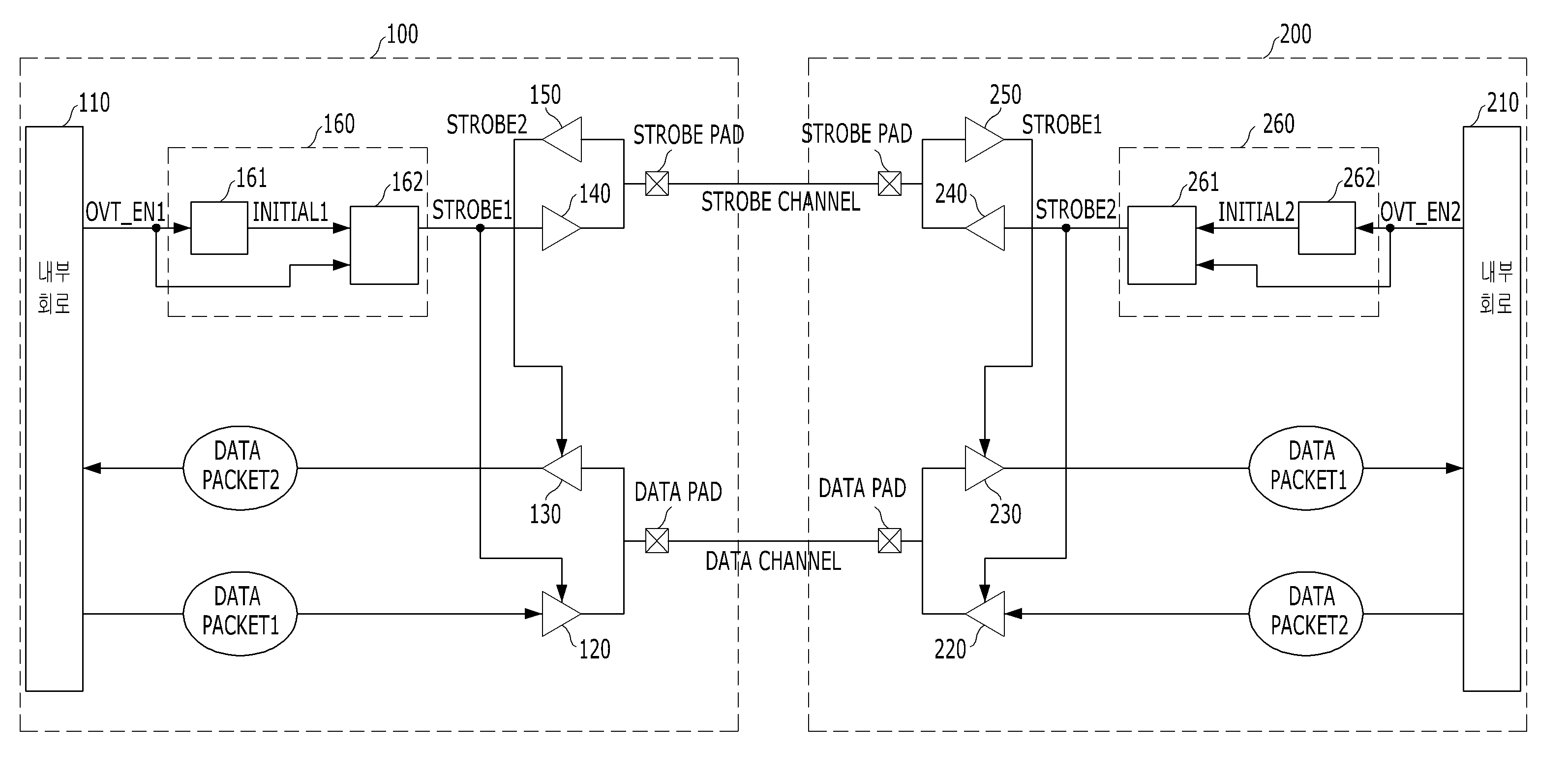
도 3은 제1칩(100)과 제2칩(200)의 제1상세 실시예를 도시한 도면이다.3 is a view showing a first detailed embodiment of the
도 3을 참조하면, 제1칩(100)은 내부회로(110), 데이터 출력회로(120), 데이터 입력회로(130), 스트로브 출력회로(140), 스트로브 입력회로(150) 및 스트로브 신호 생성부(160)를 포함한다.3, the
내부회로(110)는 제1칩(100)의 고유의 기능을 수행하는 회로이다. 제1칩(100)이 메모리라면 내부회로(110)는 데이터를 저장하는 회로와 이를 제어하는 회로를 의미하며, 제1칩(100)이 CPU라면 내부회로(110)는 각종 연산을 수행하는 회로와 이를 제어하는 회로를 의미한다. 또한, 제1칩(100)이 메모리 콘트롤러(memory controller)라면 내부회로(110)는 메모리(이 경우 제2칩(200)이 메모리가 될 것이다)를 제어하기 위한 각종 로직이 된다.The
스트로브 신호 생성부(160)는 출력 활성화신호(OUT_EN1)에 응답하여 스트로브 신호(STROBE1)를 생성한다. 출력 활성화신호(OUT_EN1)는 제1칩(100)이 데이터 패킷(DATA PACKET1)을 출력하는 구간을 나타내는 신호로 내부회로(110)에서 생성된다.The
스트로브 신호 생성부(160)는 출력 활성화신호(OUT_EN1)의 초기 활성화 구간 동안에 활성화되는 초기구간 신호(INITIAL1)를 생성하는 초기구간 신호 생성부(161)와, 출력 활성화신호(OUT_EN1)와 초기구간 신호(INITIAL1)에 응답하여 스트로브 신호(STROBE1)를 생성하는 주기파 생성부(162)를 포함하여 구성될 수 있다.The
주기파 생성부(162)가 스트로브 신호(STROBE1)를 생성하는 방법에는 다음의 2가지가 있을 수 있다. (1) 제1칩(100)에서 데이터 패킷이 출력되는 구간(즉 출력 활성화신호(OUT_EN1)의 활성화 구간)에서 스트로브 신호(STROBE1)를 생성하되, 데이터 패킷의 전송구간 중 초기구간(즉, 초기구간 신호(OUT_EN1)가 활성화된 구간)에는 스트로브 신호(STROBE1)의 주파수를 낮게 생성하고 초기구간 이후의 구간(즉, 초기구간 신호(INITIAL1)가 비활성화된 구간)에는 스트로브 신호(STROBE1)의 주파수를 높게 생성. (2) 제1칩에서 데이터 패킷이 출력되는 구간(즉, 출력 활성화신호(OUT_EN1)가 활성화된 구간)에서 스트로브 신호(STROBE1)를 생성하되, 데이터 패킷의 전송구간 중 초기구간(즉, 초기구간 신호(INITIAL1)가 활성화된 구간)에는 스트로브 신호(STROBE1)의 주파수를 점점 높이고 초기구간 이후의 구간(즉, 초기구간 신호(INITIAL1)가 비활성화된 구간)에는 스트로브 신호(STROBE1)의 주파수를 높은 주파수로 생성.There are the following two ways in which the periodic
데이터 출력회로(120)는 내부회로(110)가 제1칩(100) 외부로 출력할 데이터 패킷(DATA PACKET1)을 데이터 패드(DATA PAD)로 출력한다. 데이터 출력회로(120)는 스트로브 신호(STROBE1)에 의해 스트로브되며 데이터 패킷(DATA PACKET1)의 데이터를 출력한다. 따라서, 데이터 출력회로(120)는 데이터 패킷(DATA PACKET1)이 전송되는 구간 중 초기구간 동안에는 느린 속도로 데이터를 출력하고, 초기구간 이후에는 보다 빠른 속도로 데이터를 출력한다.The
스트로브 입력회로(150)는 제2칩(200)으로부터 제1칩(100)으로 전송되는 스트로브 신호(STROBE2)를 수신하며, 수신된 스트로브 신호(STROBE2)를 데이터 입력회로(130)로 전달한다. 그리고 데이터 입력회로(130)는 스트로브 신호(STROBE2)에 의해 스트로브되며 제2칩(200)으로부터 제1칩(100)으로 전송되는 데이터 패킷(DATA PACKET2)의 데이터를 입력받는다.The
제2칩(200)의 내부구성(210, 220, 230, 240, 250, 260)에 대한 설명은 제1칩(100)의 내부구성에 대한 설명과 동일하게 이루어질 수 있으므로, 이에 대한 상세한 설명은 생략하기로 한다.The description of the
도 3에 따르면, 제1칩(100)이 제2칩(200)으로 데이터를 전송할 때는 제1칩이 데이터 채널(DATA CHANNEL)의 데이터를 스트로브하기 위한 스트로브 신호(STROBE1)를 생성한다. 그리고, 제2칩(200)이 제1칩(100)으로 데이터를 전송할 때는 제2칩(200)이 데이터 채널(DATA CHANNEL)의 데이터를 스트로브하기 위한 스트로브 신호를 생성한다. 즉, 도 3에 따르면 전송측이 스트로브 신호를 생성하고, 전송측이 생성한 스트로브 신호를 이용하여 전송측이 데이터 패킷을 전송하고 수신측이 데이터 패킷을 수신한다.
Referring to FIG. 3, when the
도 4는 주기파 생성부(162)의 제1실시예 구성도이다.4 is a block diagram of the periodic
도 4를 참조하면, 주기파 생성부(162)는 오실레이터(410), 분주기(420) 및 스트로브 신호 공급부(430)를 포함한다.Referring to FIG. 4, the periodic
오실레이터(410)는 일정한 주파수(예, 250Mhz)를 갖는 제1클럭(CLK1)을 생성한다. 오실레이터(420)의 전력 소모를 줄이기 위해 제1칩(100)이 데이터를 출력하지 않는 동안에, 즉 출력 활성화신호(OUT_EN1)가 비활성화된 동안에 오실레이터(410)가 비활성화되도록 설계될 수도 있다. 물론, 오실레이터(410)가 항상 턴온되도록 설계될 수도 있다.The
분주기(420)는 제1클럭(CLK1)을 분주해 제1클럭(CLK1)보다 낮은 주파수(예, 125Mhz)를 갖는 제2클럭(CLK2)을 생성한다. 분주기(420)의 전력 소모를 줄이기 위해 분주기(420)가 출력 활성화신호(OUT_EN) 또는 초기구간 신호(INITIAL1) 등에 응답하여 활성화/비활성화되도록 설계될 수 있다. 도 4에서는 초기구간 신호(INITIAL)의 활성화구간 동안에 분주기(420)가 활성화되는 것으로 예시했다. 물론, 분주기(420)가 항상 턴온되도록 설계될 수도 있다.The
스트로브 신호 공급부(430)는 데이터 패킷의 전송구간 중 초기구간, 즉 초기구간 신호(INITIAL1)가 활성화된 동안, 에는 제1클럭(CLK1)을 스트로브 신호(STROBE1)로 공급한다. 그리고, 데이터 패킷의 전송구간 중 초기구간 이후의 구간, 즉 초기구간 신호(INITIAL1)가 비활성화된 동안, 에는 제2클럭(CLK2)을 스트로브 신호(STROBE1)로 공급한다. 스트로브 신호 공급부(430)는 출력 활성화신호(OUT_EN1)에 응답하여 활성화/비활성화되도록 설계될 수도 있다.
The
도 5는 주기파 생성부(162)의 제2실시예 구성도이다.5 is a block diagram of a second embodiment of the periodic
도 5를 참조하면, 주기파 생성부(162)는 제1오실레이터(510), 제2오실레이터(520) 및 스트로브 신호 공급부(530)를 포함한다.Referring to FIG. 5, the periodic
제1오실레이터(510)는 제2클럭(CLK2)보다 높은 주파수(예, 250Mhz)를 갖는 제1클럭(CLK1)을 생성한다. 제1오실레이터(510)의 전력 소모를 줄이기 위해 제1칩(100)이 데이터를 출력하지 않는 동안에, 즉 출력 활성화신호(OUT_EN1)가 비활성화된 동안에 제1오실레이터(510)가 비활성화되도록 설계될 수도 있다. 물론, 제1오실레이터(510)가 항상 턴온되도록 설계될 수도 있다.The
제2오실레이터(520)는 제1클럭(CLK1)보다 낮은 주파수(예, 200Mhz)를 갖는 제2클럭(CLK2)을 생성한다. 제2오실레이터(520)의 전력 소모를 줄이기 위해 제2오실레이터(520)가 출력 활성화신호(OUT_EN1) 또는 초기구간 신호(INITIAL1) 등에 응답하여 활성화/비활성화되도록 설계될 수도 있다.The
스트로브 신호 공급부(530)는 데이터 패킷의 전송구간 중 초기구간, 즉 초기구간 신호(INITIAL1)가 활성화된 동안, 에는 제1클럭(CLK1)을 스트로브 신호(STROBE1)로 공급한다. 그리고, 데이터 패킷의 전송구간 중 초기구간 이후의 구간, 즉 초기구간 신호(INITIAL1)가 비활성화된 동안, 에는 제2클럭(CLK2)을 스트로브 신호(STROBE1)로 공급한다. 스트로브 신호 공급부(530)는 출력 활성화신호(OUT_EN1)에 응답하여 활성화/비활성화되도록 설계될 수도 있다.
The
도 6은 주기파 생성부(163)의 제3실시예 구성도이다.6 is a block diagram of a third embodiment of the periodic wave generating unit 163.
도 6을 참조하면, 주기파 생성부(163)는 오실레이터(610)와 바이어스 전압 생성부(620)를 포함해 구성된다.Referring to FIG. 6, the periodic wave generator 163 includes an
오실레이터(610)는 입력되는 바이어스 전압(OSCBIAS)에 대응하는 주파수를 갖는 스트로브 신호(STROBE1)를 생성한다. 바이어스 전압(OSCBIAS)이 높을수록 스트로브 신호(STROBE1)의 주파수가 높아지고, 바이어스 전압(OSCBIAS)이 낮을수록 스트로브 신호(STROBE1)의 주파수가 낮아진다. 이러한 오실레이터(610)는 전압제어발진기(VCO: Voltage Controlled Oscillator)라고 잘 알려져 있다. 오실레이터(610)의 전력소모를 줄이기 위해 제1칩(100)이 데이터를 출력하지 않는 동안에, 즉 출력 활성화신호(OUT_EN1)가 비활성화된 동안에, 오실레이터(610)가 비활성화되도록 설계될 수도 있다.The
바이어스 전압 생성부(620)는 바이어스 전압(OSCBIAS)을 생성해 오실레이터(610)로 공급한다. 바이어스 전압 생성부(620)는 다음의 2가지 중 하나의 방식으로 바이어스 전압(OSCBIAS)을 생성하도록 설계될 수 있다. (1)제1칩(100)에서 데이터가 출력되는 구간(즉, 출력 활성화신호(OUT_EN1)의 활성화 구간)에서 바이어스 전압(OSCBIAS)을 생성하되, 데이터 패킷의 전송구간 중 초기구간(즉, 초기구간 신호(INITIAL1)의 활성화구간)에는 바이어스 전압(OSCBIAS)을 낮게 생성하고 초기구간 이후의 구간에서는 바이어스 전압(OSCBIAS)을 높게 생성. (2)제1칩(100)에서 데이터가 출력되는 구간(즉, 출력 활성화신호(OUT_EN1)의 활성화 구간)에서 바이어스 전압(OSCBIAS)을 생성하되, 데이터 패킷의 전송구간 중 초기구간(즉, 초기구간 신호(INITIAL1)의 활성화구간)에는 바이어스 전압(OSCBIAS)의 레벨을 점차로 높이고 초기구간 이후의 구간에서는 바이어스 전압(OSCBIAS)을 높게 생성.The
바이어스 전압 생성부(620)가 (1)과 같이 설계되는 경우에, 도 1의 주기파 생성부(162)의 스트로브 신호(STROBE1) 생성방식 중 (1)의 방식을 만족하게 된다. 그리고 바이어스 전압 생성부(620)가 (2)와 같이 설계되는 경우에, 도 1의 주기파 생성부(162)의 스트로브 신호(STROBE1) 생성방식 중 (2)의 방식을 만족하게 된다. 바이어스 전압 생성부(620)의 전류소모를 줄이기 위해 바이어스 전압 생성부(620)가 출력 활성화신호(OUT_EN1)에 응답해 활성화/비활성화되도록 설계할 수도 있다.When the
도 7a와 도 7b 각각은 (1) 및 (2)와 같이 설계된 경우에 바이어스 전압 생성부(620)에서 생성되는 바이어스 전압(OSCBIAS)의 레벨을 나타낸다.
Each of FIGS. 7A and 7B shows the level of the bias voltage OSCBIAS generated in the
도 8a와 도 8b는 도 2 내지 도 7에서 설명한 제1칩(100)으로부터 제2칩(200)으로 데이터 패킷이 전송되는 것을 도시한 타이밍도이다. 도 8a에서는 도 2a의 방법으로 데이터 패킷이 전송되는 것을 도시하였으며, 도 8b에서는 도 2b의 방법으로 데이터 패킷이 전송되는 것을 도시하였다. 또한, 도 8a와 도 8b에서는 데이터 패킷이 100개의 데이터를 포함하는 것으로 예시했다.FIGS. 8A and 8B are timing diagrams illustrating the transfer of a data packet from the
도 8a를 참조하면, 제1칩(100)으로부터 데이터 패킷(DATA PACKET1)이 출력되는 구간 동안에 출력 활성화신호(OUT_EN1)가 '하이'레벨로 활성화된다. 그리고 초기구간 신호(INITIAL1)가 출력 활성화신호(OUT_EN)의 활성화 초기구간 동안에 '하이'레벨로 활성화된다. 스트로브 신호(STROBE1)는 초기구간 신호(INITIAL1)가 활성화되어있는 동안에는 200Mhz로 토글하며, 초기구간 신호(INITIAL1)가 비활성화되어 있는 동안에는 250Mhz로 토글한다. 제1칩(100)의 데이터 출력회로(120)는 스트로브 신호(STROBE1)에 응답하여 데이터 패킷(D00~D99)의 데이터를 출력한다. 초기구간 동안에 출력되는 4개의 데이터(D00~D03)는 200Mhz로 토글하는 스트로브 신호(STROBE1)의 '하이'구간과 '로우'구간에서 출력된다. 즉, 초기구간 동안에 출력되는 4개의 데이터(D00~D03)는 400Mhz의 속도로 출력된다. 초기구간 이후에 출력되는 나머지 데이터(D04~D99)는 250Mhz로 토글하는 스트로브 신호(STROBE1)의 '하이'구간과 '로우'구간에서 출력되므로 500Mhz의 속도로 출력된다. 제2칩(200)의 데이터 입력회로(230)는 스트로브 신호(STROBE1)에 응답하여 데이터 패킷(D00~D99)을 입력받는다.Referring to FIG. 8A, the output enable signal OUT_EN1 is activated to a high level during a period in which a data packet (DATA PACKET1) is output from the
도 8b를 참조하면, 제1칩(100)으로부터 데이터 패킷(DATA PACKET1)이 출력되는 구간 동안에 출력 활성화신호(OUT_EN1)가 '하이'레벨로 활성화된다. 그리고 초기구간 신호(INITIAL1)가 출력 활성화신호(OUT_EN)의 활성화 초기구간 동안에 '하이'레벨로 활성화된다. 스트로브 신호(STROBE1)는 초기구간 신호(INITIAL1)가 활성화되어있는 동안에는 200Mhz로부터 250Mhz로 주파수를 높여가며 토글하며, 초기구간 신호(INITIAL1)가 비활성화되어 있는 동안에는 250Mhz로 토글한다. 제1칩(100)의 데이터 출력회로(120)는 스트로브 신호(STROBE1)에 응답하여 데이터 패킷(D00~D99)의 데이터를 출력한다. 초기구간 동안에 출력되는 4개의 데이터(D00~D03)는 200Mhz로부터 250Mhz로 주파수가 높아지며 토글하는 스트로브 신호(STROBE1)의 '하이'구간과 '로우'구간에서 출력된다. 즉, 초기구간 동안에 출력되는 4개의 데이터(D00~D03)는 400Mhz로부터 500Mhz로 속도가 높아지며 출력된다. 초기구간 이후에 출력되는 나머지 데이터(D04~D99)는 250Mhz로 토글하는 스트로브 신호(STROBE1)의 '하이'구간과 '로우'구간에서 출력되므로 500Mhz의 속도로 출력된다. 제2칩(200)의 데이터 입력회로(230)는 스트로브 신호(STROBE1)에 응답하여 데이터 패킷(D00~D99)을 입력받는다.
Referring to FIG. 8B, the output enable signal OUT_EN1 is activated to a high level during a period in which the data packet (DATA PACKET1) is output from the
도 9는 제1칩(100)과 제2칩(200)의 제2상세 실시예 구성도이다.9 is a configuration diagram of the first and
도 3에서는 제1칩(100)에서 제2칩(200)으로 데이터가 전송되는 경우에는 제1칩(100)에서 스트로브 신호(STROBE1)를 생성하고, 제2칩(200)에서 제1칩(100)으로 데이터가 전송되는 경우에는 제2칩(200)에서 스트로브 신호(STROBE2)를 생성하는 경우를 도시했다. 도 9에서는 두 칩 중 하나의 칩(100)에서만 스트로브 신호(STROBE)를 생성하는 경우를 도시한다.3, when data is transmitted from the
제1칩은 내부회로(910), 데이터 출력회로(920), 데이터 입력회로(930), 스트로브 출력회로(940) 및 스트로브 신호 생성부(960)를 포함한다.The first chip includes an
내부회로(910)는 제1칩(100)의 고유의 기능을 수행하는 회로이다. 제1칩(100)이 메모리라면 내부회로(910)는 데이터를 저장하는 회로와 이를 제어하는 회로를 의미하며, 제1칩(100)이 CPU라면 내부회로(910)는 각종 연산을 수행하는 회로와 이를 제어하는 회로를 의미한다. 또한, 제1칩(100)이 메모리 콘트롤러(memory controller)라면 내부회로(910)는 메모리(이 경우 제2칩(200)이 메모리가 될 것이다)를 제어하기 위한 각종 로직이 된다.The
스트로브 신호 생성부(960)는 입/출력 활성화신호(INOUT_EN)에 응답하여 스트로브 신호(STROBE)를 생성한다. 입/출력 활성화신호(INOUT_EN)는 제1칩(100)이 데이터 패킷(DATA PACKET1)을 출력하는 구간과 제2칩(200)이 데이터 패킷(DATA PACKET2)을 출력하는 구간(즉, 제1칩(100)이 데이터 패킷(DATA PACKET2)을 입력받는 구간)을 나타내는 신호로 내부회로(960)에서 생성된다. 즉, 스트로브 신호 생성부(960)는 제1칩(100)에서 제2칩(200)으로 데이터가 전송되는 구간에서도 스트로브 신호(STROBE)를 생성하고 제2칩(200)에서 제1칩(100)으로 데이터가 전송되는 구간에서도 스트로브 신호(STROBE)를 생성한다.The
스트로브 신호 생성부(960)는 입/출력 활성화신호(OUT_EN)의 초기 활성화 구간 동안에 활성화되는 초기구간 신호(INITIAL)를 생성하는 초기구간 신호 생성부(961)와, 입/출력 활성화신호(OUT_EN)와 초기구간 신호(INITIAL1)에 응답하여 스트로브 신호(STROBE)를 생성하는 주기파 생성부(962)를 포함하여 구성될 수 있다. 주기파 생성부(962)는 도 4 내지 도 7에서 설명한 것과 동일한 방식으로 구성될 수 있다. 다만, 도 4 내지 도 7의 출력 활성화신호(OUT_EN1)를 입/출력 활성화신호(INOUT_EN)로 대체하고, 초기구간 신호(INITIAL1)를 초기구간 신호(INITIAL)로 대체하면 된다.The
데이터 출력회로(920)는 내부회로(910)가 제1칩(100) 외부로 출력할 데이터 패킷(DATA PACKET1)을 데이터 패드(DATA PAD)로 출력한다. 데이터 출력회로(920)는 스트로브 신호(STROBE)에 의해 스트로브되며 데이터 패킷(DATA PACKET1)의 데이터를 출력한다. 따라서, 데이터 출력회로(920)는 데이터 패킷(DATA PACKET1)이 전송되는 구간 중 초기구간 동안에는 느린 속도로 데이터를 출력하고, 초기구간 이후에는 보다 빠른 속도로 데이터를 출력한다.The
데이터 입력회로(930)는 스트로브 신호(STROBE)에 의해 스트로브되며 제2칩(200)으로부터 제1칩(100)으로 전송되는 데이터 패킷(DATA PACKET2)의 데이터를 입력받는다.The
제2칩(200)은 내부회로(910), 데이터 출력회로(920), 데이터 입력회로(930) 및 스트로브 입력회로(950)를 포함한다. 제2칩(200)은 데이터 입/출력동작시 스트로브 입력회로(950)를 통해 제1칩(100)으로부터 전달받은 스트로브 신호(STROBE)를 사용한다. 즉, 제2칩(200)은 자체적으로 스트로브 신호를 생성하지 않으며, 데이터 출력회로(920)와 데이터 입력회로(910) 모두가 제1칩(100)으로부터 전달된 스트로브 신호(STROBE)를 사용한다.
The
본 발명의 기술사상은 상기 바람직한 실시예에 따라 구체적으로 기술되었으나, 상기한 실시예는 그 설명을 위한 것이며 그 제한을 위한 것이 아님을 주의하여야 한다. 또한, 본 발명의 기술분야에서 통상의 전문가라면 본 발명의 기술사상의 범위 내에서 다양한 실시예가 가능함을 알 수 있을 것이다.
While the present invention has been particularly shown and described with reference to exemplary embodiments thereof, it is to be understood that the invention is not limited to the disclosed exemplary embodiments. It will be apparent to those skilled in the art that various modifications and variations can be made in the present invention without departing from the spirit and scope of the invention.
100: 제1칩 200: 제2칩
DATA CHANNEL: 데이터 채널 STROBE CHANNEL: 스트로브 채널
110, 210: 내부회로 120, 220: 데이터 출력회로
130, 230: 데이터 입력회로 140, 240: 스트로브 출력회로
150, 250: 스트로브 입력회로 160, 260: 스트로브 신호 생성부100: first chip 200: second chip
DATA CHANNEL: Data channel STROBE CHANNEL: Strobe channel
110, 210:
130, 230:
150, 250:
Claims (25)
스트로브 신호에 응답해 상기 내부회로의 데이터 패킷을 칩 외부로 출력하기 위한 데이터 출력회로;
바이어스 전압에 대응하는 주파수를 갖는 상기 스트로브 신호를 생성하는 오실레이터; 및
상기 데이터 패킷의 전송구간 중 초기구간에는 상기 바이어스 전압이 점차로 높아지도록 생성하고, 상기 초기구간 이후에는 상기 바이어스 전압이 일정 전압레벨을 유지하도록 생성하는 바이어스 전압 생성부
를 포함하는 집적회로 칩.
Internal circuit;
A data output circuit for outputting a data packet of the internal circuit to the outside of the chip in response to a strobe signal;
An oscillator for generating the strobe signal having a frequency corresponding to a bias voltage; And
A bias voltage generator for generating the bias voltage so that the bias voltage gradually increases in an initial period of the transmission period of the data packet and generating the bias voltage to maintain a constant voltage level after the initial period;
≪ / RTI >
상기 일정 전압레벨은 상기 초기구간에서의 마지막 바이어스 전압 레벨과 동일한
집적회로 칩.
16. The method of claim 15,
The constant voltage level is equal to the last bias voltage level in the initial period
Integrated circuit chip.
상기 오실레이터는 상기 데이터 패킷의 전송구간에서 활성화되는
집적회로 칩.
16. The method of claim 15,
The oscillator is activated in the transmission interval of the data packet
Integrated circuit chip.
상기 내부회로는 상기 데이터 패킷의 전송구간을 나타내는 출력 활성화신호를 생성하고,
상기 집적회로 칩은 상기 출력 활성화신호의 초기 활성화구간 동안에 활성화되는 초기구간 신호를 생성하는 초기구간 신호 생성부를 더 포함하고,
상기 바이어스 전압 생성부는 상기 초기구간 신호가 활성화된 동안에 상기 바이어스 전압이 점차로 높아지도록 생성하는
집적회로 칩.
16. The method of claim 15,
The internal circuit generates an output activation signal indicating a transmission period of the data packet,
Wherein the integrated circuit chip further includes an initial section signal generator for generating an initial section signal activated during an initial activation section of the output activation signal,
The bias voltage generator generates the bias voltage so that the bias voltage gradually increases while the initial interval signal is activated
Integrated circuit chip.
제2칩; 및
상기 제1칩과 제2칩 간의 데이터 채널을 포함하고,
상기 제1칩은
내부회로;
스트로브 신호에 응답해 상기 내부회로의 데이터 패킷을 상기 데이터 채널로 출력하기 위한 데이터 출력회로;
바이어스 전압에 대응하는 주파수를 갖는 상기 스트로브 신호를 생성하는 오실레이터; 및
상기 데이터 패킷의 전송구간 중 초기구간에는 상기 바이어스 전압 레벨이 점차로 높아지도록 생성하고, 상기 초기구간 이후에는 상기 바이어스 전압이 일정 전압레벨을 유지하도록 생성하는 바이어스 전압 생성부
를 포함하는 제1칩과 제2칩을 포함하는 시스템.
A first chip;
A second chip; And
A data channel between the first chip and the second chip,
The first chip
Internal circuit;
A data output circuit for outputting a data packet of the internal circuit to the data channel in response to a strobe signal;
An oscillator for generating the strobe signal having a frequency corresponding to a bias voltage; And
A bias voltage generator for generating the bias voltage level so as to gradually increase in an initial period of the transmission period of the data packet and generating the bias voltage to maintain a constant voltage level after the initial period,
A first chip and a second chip.
상기 일정 전압레벨은 상기 초기구간에서의 마지막 바이어스 전압 레벨과 동일한
제1칩과 제2칩을 포함하는 시스템.
25. The method of claim 24,
The constant voltage level is equal to the last bias voltage level in the initial period
A system comprising a first chip and a second chip.
Priority Applications (4)
| Application Number | Priority Date | Filing Date | Title |
|---|---|---|---|
| KR1020110109344A KR101898150B1 (en) | 2011-10-25 | 2011-10-25 | Integrated circuit chip and system including the same |
| US13/610,760 US8624639B2 (en) | 2011-10-25 | 2012-09-11 | Integrated circuit chip and system having the same |
| US14/145,539 US8786326B2 (en) | 2011-10-25 | 2013-12-31 | Integrated circuit chip and system having the same |
| US14/145,489 US8786325B2 (en) | 2011-10-25 | 2013-12-31 | Integrated circuit chip and system having the same |
Applications Claiming Priority (1)
| Application Number | Priority Date | Filing Date | Title |
|---|---|---|---|
| KR1020110109344A KR101898150B1 (en) | 2011-10-25 | 2011-10-25 | Integrated circuit chip and system including the same |
Publications (2)
| Publication Number | Publication Date |
|---|---|
| KR20130044956A KR20130044956A (en) | 2013-05-03 |
| KR101898150B1 true KR101898150B1 (en) | 2018-09-13 |
Family
ID=48135455
Family Applications (1)
| Application Number | Title | Priority Date | Filing Date |
|---|---|---|---|
| KR1020110109344A Active KR101898150B1 (en) | 2011-10-25 | 2011-10-25 | Integrated circuit chip and system including the same |
Country Status (2)
| Country | Link |
|---|---|
| US (3) | US8624639B2 (en) |
| KR (1) | KR101898150B1 (en) |
Families Citing this family (3)
| Publication number | Priority date | Publication date | Assignee | Title |
|---|---|---|---|---|
| KR101898150B1 (en) * | 2011-10-25 | 2018-09-13 | 에스케이하이닉스 주식회사 | Integrated circuit chip and system including the same |
| US10223198B2 (en) * | 2016-02-18 | 2019-03-05 | Micron Technology, Inc. | Error rate reduction |
| EP3433929A1 (en) * | 2016-03-22 | 2019-01-30 | Telefonaktiebolaget LM Ericsson (PUBL) | Low power high speed interface |
Citations (1)
| Publication number | Priority date | Publication date | Assignee | Title |
|---|---|---|---|---|
| JP2010231542A (en) * | 2009-03-27 | 2010-10-14 | Oki Semiconductor Co Ltd | Semiconductor integrated circuit device |
Family Cites Families (18)
| Publication number | Priority date | Publication date | Assignee | Title |
|---|---|---|---|---|
| US4549094A (en) * | 1983-10-07 | 1985-10-22 | United Technologies Automotive, Inc. | Debounce circuit providing synchronously clocked digital signals |
| US4939389A (en) * | 1988-09-02 | 1990-07-03 | International Business Machines Corporation | VLSI performance compensation for off-chip drivers and clock generation |
| US5905391A (en) * | 1997-07-14 | 1999-05-18 | Intel Corporation | Master-slave delay locked loop for accurate delay or non-periodic signals |
| US6727728B1 (en) * | 1997-12-30 | 2004-04-27 | Lsi Logic Corporation | XOR circuit |
| JPH11328955A (en) * | 1998-05-14 | 1999-11-30 | Mitsubishi Electric Corp | Semiconductor circuit device |
| JP3814470B2 (en) * | 2000-08-09 | 2006-08-30 | 富士通株式会社 | Data transfer method and data transfer apparatus |
| US6918048B2 (en) * | 2001-06-28 | 2005-07-12 | Intel Corporation | System and method for delaying a strobe signal based on a slave delay base and a master delay adjustment |
| US7308524B2 (en) * | 2003-01-13 | 2007-12-11 | Silicon Pipe, Inc | Memory chain |
| US7126378B2 (en) * | 2003-12-17 | 2006-10-24 | Rambus, Inc. | High speed signaling system with adaptive transmit pre-emphasis |
| CA2731265A1 (en) * | 2003-12-08 | 2005-06-23 | Qualcomm Incorporated | High data rate interface with improved link synchronization |
| US7233164B2 (en) * | 2003-12-17 | 2007-06-19 | Rambus Inc. | Offset cancellation in a multi-level signaling system |
| US8121237B2 (en) * | 2006-03-16 | 2012-02-21 | Rambus Inc. | Signaling system with adaptive timing calibration |
| KR100805004B1 (en) * | 2006-06-15 | 2008-02-20 | 주식회사 하이닉스반도체 | A data strobe signal generator for generating a data strobe signal based on an adjustable preamble value and a semiconductor memory device including the same |
| US8793525B2 (en) * | 2007-10-22 | 2014-07-29 | Rambus Inc. | Low-power source-synchronous signaling |
| US7974589B2 (en) * | 2008-02-13 | 2011-07-05 | Analog Devices, Inc. | High-speed data transmitters |
| JP2012515377A (en) * | 2009-01-12 | 2012-07-05 | ラムバス・インコーポレーテッド | Clock transfer low power signaling system |
| US9046898B2 (en) * | 2011-02-24 | 2015-06-02 | Google Inc. | Power-preserving communications architecture with long-polling persistent cloud channel for wireless network-connected thermostat |
| KR101898150B1 (en) * | 2011-10-25 | 2018-09-13 | 에스케이하이닉스 주식회사 | Integrated circuit chip and system including the same |
-
2011
- 2011-10-25 KR KR1020110109344A patent/KR101898150B1/en active Active
-
2012
- 2012-09-11 US US13/610,760 patent/US8624639B2/en active Active
-
2013
- 2013-12-31 US US14/145,539 patent/US8786326B2/en active Active
- 2013-12-31 US US14/145,489 patent/US8786325B2/en active Active
Patent Citations (1)
| Publication number | Priority date | Publication date | Assignee | Title |
|---|---|---|---|---|
| JP2010231542A (en) * | 2009-03-27 | 2010-10-14 | Oki Semiconductor Co Ltd | Semiconductor integrated circuit device |
Also Published As
| Publication number | Publication date |
|---|---|
| US8624639B2 (en) | 2014-01-07 |
| US20130099833A1 (en) | 2013-04-25 |
| US8786326B2 (en) | 2014-07-22 |
| US20140111255A1 (en) | 2014-04-24 |
| KR20130044956A (en) | 2013-05-03 |
| US8786325B2 (en) | 2014-07-22 |
| US20140111254A1 (en) | 2014-04-24 |
Similar Documents
| Publication | Publication Date | Title |
|---|---|---|
| US10678556B2 (en) | Integrated circuit device including wake-up control circuit and electronic device including the same | |
| US11181941B2 (en) | Using a stuttered clock signal to reduce self-induced voltage noise | |
| CN104183265B (en) | Circuit of dynamic random access memory device and clock control method thereof | |
| US8754681B2 (en) | Multi-part clock management | |
| KR20150040170A (en) | Storage device based on flash memory and method for operating thereof | |
| US10013376B2 (en) | System including interface circuit for driving data transmission line to termination voltage | |
| KR101898150B1 (en) | Integrated circuit chip and system including the same | |
| US10146251B2 (en) | Semiconductor device | |
| KR100933257B1 (en) | Semiconductor memory device | |
| KR101138832B1 (en) | Semiconductor memory device and method operating the same | |
| KR20130097574A (en) | Command decoder | |
| CN101441497B (en) | Information processing apparatus having memory clock setting function and memory clock setting method | |
| EP1058180A2 (en) | Control circuit having clock control unit | |
| KR101239682B1 (en) | Internal voltage geneation circuit and semiconductor integrated circuit | |
| KR101185550B1 (en) | System including chips, integrated circuit chip and method for transferring a data packet | |
| KR20130044957A (en) | Integrated circuit systam and operartion method of memory system | |
| KR101506337B1 (en) | Smart card system and method of driving the same | |
| CN1937075B (en) | Data transfer operation completion detection circuit and semiconductor memory device provided therewith | |
| TWI540441B (en) | Electronic system in synchronous with peripheral device | |
| CN114115508B (en) | Data reading method and device, and storage medium | |
| TW201445439A (en) | Method of accessing on-chip read only memory and computer system thereof | |
| JP2009259114A (en) | System semiconductor device | |
| KR101735082B1 (en) | Circuit and method for delaying internal write signal of memory device | |
| KR101346185B1 (en) | A RTC module and a computer system including thereof | |
| JP2009272964A (en) | Communication system, host, client, phone body of cellular phone, battery and communication method |
Legal Events
| Date | Code | Title | Description |
|---|---|---|---|
| PA0109 | Patent application |
St.27 status event code: A-0-1-A10-A12-nap-PA0109 |
|
| PN2301 | Change of applicant |
St.27 status event code: A-3-3-R10-R13-asn-PN2301 St.27 status event code: A-3-3-R10-R11-asn-PN2301 |
|
| PN2301 | Change of applicant |
St.27 status event code: A-3-3-R10-R13-asn-PN2301 St.27 status event code: A-3-3-R10-R11-asn-PN2301 |
|
| PG1501 | Laying open of application |
St.27 status event code: A-1-1-Q10-Q12-nap-PG1501 |
|
| PN2301 | Change of applicant |
St.27 status event code: A-3-3-R10-R13-asn-PN2301 St.27 status event code: A-3-3-R10-R11-asn-PN2301 |
|
| A201 | Request for examination | ||
| PA0201 | Request for examination |
St.27 status event code: A-1-2-D10-D11-exm-PA0201 |
|
| E902 | Notification of reason for refusal | ||
| PE0902 | Notice of grounds for rejection |
St.27 status event code: A-1-2-D10-D21-exm-PE0902 |
|
| E13-X000 | Pre-grant limitation requested |
St.27 status event code: A-2-3-E10-E13-lim-X000 |
|
| P11-X000 | Amendment of application requested |
St.27 status event code: A-2-2-P10-P11-nap-X000 |
|
| P13-X000 | Application amended |
St.27 status event code: A-2-2-P10-P13-nap-X000 |
|
| E701 | Decision to grant or registration of patent right | ||
| PE0701 | Decision of registration |
St.27 status event code: A-1-2-D10-D22-exm-PE0701 |
|
| GRNT | Written decision to grant | ||
| PR0701 | Registration of establishment |
St.27 status event code: A-2-4-F10-F11-exm-PR0701 |
|
| PR1002 | Payment of registration fee |
St.27 status event code: A-2-2-U10-U11-oth-PR1002 Fee payment year number: 1 |
|
| PG1601 | Publication of registration |
St.27 status event code: A-4-4-Q10-Q13-nap-PG1601 |
|
| PR1001 | Payment of annual fee |
St.27 status event code: A-4-4-U10-U11-oth-PR1001 Fee payment year number: 4 |
|
| PR1001 | Payment of annual fee |
St.27 status event code: A-4-4-U10-U11-oth-PR1001 Fee payment year number: 5 |
|
| PR1001 | Payment of annual fee |
St.27 status event code: A-4-4-U10-U11-oth-PR1001 Fee payment year number: 6 |
|
| PR1001 | Payment of annual fee |
St.27 status event code: A-4-4-U10-U11-oth-PR1001 Fee payment year number: 7 |
|
| PR1001 | Payment of annual fee |
St.27 status event code: A-4-4-U10-U11-oth-PR1001 Fee payment year number: 8 |
|
| U11 | Full renewal or maintenance fee paid |
Free format text: ST27 STATUS EVENT CODE: A-4-4-U10-U11-OTH-PR1001 (AS PROVIDED BY THE NATIONAL OFFICE) Year of fee payment: 8 |