KR101892958B1 - Plasma processing apparatus - Google Patents
Plasma processing apparatus Download PDFInfo
- Publication number
- KR101892958B1 KR101892958B1 KR1020110112588A KR20110112588A KR101892958B1 KR 101892958 B1 KR101892958 B1 KR 101892958B1 KR 1020110112588 A KR1020110112588 A KR 1020110112588A KR 20110112588 A KR20110112588 A KR 20110112588A KR 101892958 B1 KR101892958 B1 KR 101892958B1
- Authority
- KR
- South Korea
- Prior art keywords
- gas
- space
- isolation space
- processing chamber
- forming member
- Prior art date
- Legal status (The legal status is an assumption and is not a legal conclusion. Google has not performed a legal analysis and makes no representation as to the accuracy of the status listed.)
- Expired - Fee Related
Links
Images


Classifications
-
- H—ELECTRICITY
- H01—ELECTRIC ELEMENTS
- H01J—ELECTRIC DISCHARGE TUBES OR DISCHARGE LAMPS
- H01J37/00—Discharge tubes with provision for introducing objects or material to be exposed to the discharge, e.g. for the purpose of examination or processing thereof
- H01J37/32—Gas-filled discharge tubes
- H01J37/32431—Constructional details of the reactor
- H01J37/3244—Gas supply means
-
- H—ELECTRICITY
- H01—ELECTRIC ELEMENTS
- H01J—ELECTRIC DISCHARGE TUBES OR DISCHARGE LAMPS
- H01J37/00—Discharge tubes with provision for introducing objects or material to be exposed to the discharge, e.g. for the purpose of examination or processing thereof
- H01J37/32—Gas-filled discharge tubes
- H01J37/32009—Arrangements for generation of plasma specially adapted for examination or treatment of objects, e.g. plasma sources
- H01J37/32082—Radio frequency generated discharge
- H01J37/32091—Radio frequency generated discharge the radio frequency energy being capacitively coupled to the plasma
-
- H—ELECTRICITY
- H01—ELECTRIC ELEMENTS
- H01J—ELECTRIC DISCHARGE TUBES OR DISCHARGE LAMPS
- H01J37/00—Discharge tubes with provision for introducing objects or material to be exposed to the discharge, e.g. for the purpose of examination or processing thereof
- H01J37/32—Gas-filled discharge tubes
- H01J37/32431—Constructional details of the reactor
- H01J37/32532—Electrodes
- H01J37/32568—Relative arrangement or disposition of electrodes; moving means
Landscapes
- Physics & Mathematics (AREA)
- Engineering & Computer Science (AREA)
- Plasma & Fusion (AREA)
- Chemical & Material Sciences (AREA)
- Analytical Chemistry (AREA)
- Drying Of Semiconductors (AREA)
- Plasma Technology (AREA)
- Chemical Vapour Deposition (AREA)
Abstract
(과제) 샤워 헤드의 이면(裏面)측 공간에 있어서의 이상(異常) 방전 등의 플라즈마 처리에 악영향을 미치는 현상의 발생을 억제할 수 있어, 양호한 플라즈마 처리를 안정적으로 행할 수 있는 플라즈마 처리 장치를 제공한다.
(해결 수단) 처리 챔버 내에 설치되어, 기판 재치대를 겸한 하부 전극과, 가스를 공급하는 샤워 헤드로서의 기능을 구비하고, 또한 상하 이동 가능하게 된 상부 전극과, 상부 전극의 상측에 설치되어 처리 챔버의 상부 개구를 기밀하게 폐색하는 덮개체와, 상부 전극과 덮개체와의 사이의 공간을 폐색하도록 설치되어, 내측에 외측과 격리된 격리 공간을 형성함과 함께, 내부에 기체를 도입·배출하기 위한 도입·배출구를 갖고, 상부 전극의 상하 이동에 따라서 격리 공간의 용적이 변동 가능하게 된 격리 공간 형성 부재와, 격리 공간 형성 부재의 격리 공간에 기체를 공급 및, 배출하는 기체 공급 배출 기구를 구비하고 있다.A plasma processing apparatus capable of suppressing the occurrence of a phenomenon adversely affecting plasma processing such as abnormal discharge in a space on the rear surface side of a showerhead and capable of stably performing good plasma processing to provide.
A lower electrode provided in the processing chamber and serving also as a substrate mounting table and a function as a showerhead for supplying a gas and having a vertically movable upper electrode and a lower electrode provided above the upper electrode, A cover body for hermetically closing the upper opening of the upper electrode, and an insulating space isolated from the outside on the inner side so as to close a space between the upper electrode and the cover body, And a gas supply / discharge mechanism for supplying and discharging the gas to / from the isolation space of the isolation space formation member is provided .
Description
본 발명은, 플라즈마 처리 장치에 관한 것이다.The present invention relates to a plasma processing apparatus.
종래부터, 반도체 장치의 제조 분야 등에 있어서는, 반도체 웨이퍼 등의 기판을 향하여 가스를 샤워 형상으로 공급하기 위한 샤워 헤드가 이용되고 있다. 즉, 예를 들면 반도체 웨이퍼 등의 기판에 플라즈마 에칭 처리를 행하는 플라즈마 처리 장치에서는, 처리 챔버 내에, 기판을 올려놓기 위한 재치대가 설치되어 있고, 이 재치대와 대향하도록 샤워 헤드가 설치되어 있다. 이 샤워 헤드에는, 재치대와 대향하는 대향면에, 가스 토출공이 복수 형성되어 있어, 이들 가스 토출공으로부터 기판을 향하여 가스를 샤워 형상으로 공급한다.2. Description of the Related Art Conventionally, in the field of manufacturing semiconductor devices and the like, a showerhead for supplying a gas in a shower shape toward a substrate such as a semiconductor wafer is used. That is, for example, in a plasma processing apparatus for performing a plasma etching treatment on a substrate such as a semiconductor wafer, a table for placing a substrate thereon is provided in the processing chamber, and a shower head is provided so as to face the table. The shower head has a plurality of gas discharging holes formed in opposing surfaces facing the mounting table, and supplies the gas from the gas discharging holes toward the substrate in a shower shape.
상기한 플라즈마 처리 장치에서는, 처리 챔버 내의 가스의 흐름을 균일화하기 위해, 재치대의 주위로부터 하방으로 배기를 행하는 구성으로 한 것이 알려져 있다. 또한, 상부 전극으로서 기능하는 샤워 헤드와, 하부 전극으로서 기능하는 재치대와의 간격을 변경할 수 있도록 구성된 플라즈마 처리 장치가 알려져 있다(예를 들면, 특허문헌 1 참조).In the plasma processing apparatus described above, it is known that the exhaust gas is exhausted from the periphery of the mounting table downward in order to uniform the flow of the gas in the processing chamber. Further, there is known a plasma processing apparatus configured to change a distance between a showerhead functioning as an upper electrode and a table serving as a lower electrode (see, for example, Patent Document 1).
상기의 플라즈마 처리 장치에 있어서, 예를 들면, 상부 전극으로서의 샤워 헤드를 상하 이동시켜 하부 전극으로서의 재치대와의 간격을 변경하도록 한 경우, 샤워 헤드를 사이에 두고 처리 공간과 반대측(이면(裏面)측)에, 처리 공간의 크기의 변동에 수반하여 크기가 변동하는 공간(이면측 공간)이 필요해진다. 그러나, 이러한 이면측 공간이, 플라즈마 처리에 악영향을 미치는 경우가 있다.In the above-described plasma processing apparatus, for example, when the showerhead as the upper electrode is moved up and down to change the interval between the showerhead as the lower electrode and the showerhead, (Back side space) in which the size fluctuates along with the variation in the size of the processing space. However, such a back side space may adversely affect the plasma processing.
즉, 이 이면측 공간에 있어서 이상(異常) 방전이 발생하는 경우가 있으며, 이 이상 방전에 의해 처리 공간의 플라즈마의 상태가 변화해 버린다는 문제나, 이상 방전이 오염의 원인이 된다는 문제가 발생한다. 또한, 이면측 공간에 처리 가스가 유입되면, 처리 공간에 있어서의 플라즈마의 밀도나 이온의 양이 저감하거나 데포지션(deposition)이 되어 이면측 공간의 벽면에 부착하는 등의 문제도 발생한다. 이러한 문제는, 에칭 처리의 경우 외에, 성막 처리의 경우에 대해서도 동일하게 하여 발생한다.That is, an abnormal discharge may occur in the back side space. This abnormal discharge causes a problem that the state of the plasma in the processing space changes, and a problem that the abnormal discharge causes contamination do. Further, when the processing gas flows into the back side space, there arises a problem that the density of the plasma and the amount of ions in the processing space are reduced or adhered to the wall surface of the back side space due to deposition. This problem occurs in the same manner in the case of the film forming process in addition to the etching process.
본 발명은, 상기 종래의 사정에 대처하여 이루어진 것으로, 샤워 헤드를 상하 이동시켜 하부 전극과의 간격을 변경 가능하게 한 구성에 있어서, 샤워 헤드의 이면측 공간에 있어서의 이상 방전 등의 플라즈마 처리에 악영향을 미치는 현상의 발생을 억제할 수 있어, 양호한 플라즈마 처리를 안정적으로 행할 수 있는 플라즈마 처리 장치를 제공하려고 하는 것이다.SUMMARY OF THE INVENTION The present invention has been made in order to solve the above-mentioned conventional problems, and it is an object of the present invention to provide a plasma processing apparatus and a plasma processing method, It is possible to suppress occurrence of a phenomenon adversely affecting the plasma processing apparatus and to provide a plasma processing apparatus capable of stably performing good plasma processing.
본 발명의 플라즈마 처리 장치는, 기판을 수용하여 플라즈마 처리를 행하기 위한 처리 챔버와, 상기 처리 챔버 내에 설치되어, 상기 기판을 올려놓기 위한 재치대를 겸한 하부 전극과, 상기 처리 챔버 내에 설치되어, 상기 하부 전극과 대향하여, 상기 하부 전극과의 사이에 처리 공간을 형성함과 함께 상기 하부 전극과 대향하는 대향면에 복수 형성된 가스 토출공으로부터 상기 기판을 향하여 처리 가스를 공급하는 샤워 헤드로서의 기능을 구비하고, 또한 상하 이동 가능하게 되어 상기 하부 전극과의 간격이 변경 가능하게 된 상부 전극과, 상기 상부 전극의 상측에 설치되어 상기 처리 챔버의 상부 개구를 기밀하게 폐색하는 덮개체와, 상기 상부 전극과 상기 덮개체와의 사이의 공간을 폐색하도록 설치되어, 내측에 외측과 격리된 격리 공간을 형성함과 함께, 내부에 기체를 도입·배출하기 위한 도입·배출구를 갖고, 상기 상부 전극의 상하 이동에 따라서 상기 격리 공간의 용적이 변동 가능하게 된 격리 공간 형성 부재와, 상기 격리 공간 형성 부재의 상기 격리 공간에, 상기 도입·배출구로부터 기체를 공급 및 배출하는 기체 공급 배출 기구와, 상기 상부 전극과 상기 하부 전극과의 사이에 고주파 전력을 공급하여 상기 처리 가스의 플라즈마를 발생시키는 고주파 전원을 구비한 것을 특징으로 한다.A plasma processing apparatus of the present invention includes a processing chamber for accommodating a substrate and performing a plasma process, a lower electrode provided in the processing chamber and serving also as a mount for loading the substrate, A function as a showerhead for forming a processing space between the lower electrode and the lower electrode and supplying a process gas from the plurality of gas discharge holes formed on the opposing surface facing the lower electrode toward the substrate, An upper electrode disposed above the upper electrode to hermetically seal the upper opening of the processing chamber, and a lower electrode provided on the lower electrode, And an insulating space isolated from the outside is formed on the inner side so as to close the space between the cover and the cover body An insulating space forming member having an inlet and an outlet for introducing and discharging gas into and from the inside of the insulating space forming member and capable of changing the volume of the insulating space in accordance with the upward and downward movement of the upper electrode; And a high frequency power source for generating a plasma of the process gas by supplying a high frequency power between the upper electrode and the lower electrode is characterized by having a gas supply and discharge mechanism for supplying and discharging gas from the inlet and the outlet, .
본 발명에 의하면, 샤워 헤드를 상하 이동시켜 하부 전극과의 간격을 변경 가능하게 한 구성에 있어서, 샤워 헤드의 이면측 공간에 있어서의 이상 방전 등의 플라즈마 처리에 악영향을 미치는 현상의 발생을 억제할 수 있어, 양호한 플라즈마 처리를 안정적으로 행할 수 있는 플라즈마 처리 장치를 제공할 수 있다.According to the present invention, in the configuration in which the distance between the shower head and the lower electrode can be changed by moving the shower head up and down, occurrence of a phenomenon that adversely affects the plasma processing such as abnormal discharge in the space on the back side of the showerhead is suppressed It is possible to provide a plasma processing apparatus capable of stably performing good plasma processing.
도 1은 본 발명의 제1 실시 형태에 따른 플라즈마 처리 장치의 구성을 나타내는 종단면도이다.
도 2는 도 1의 플라즈마 처리 장치의 요부 구성을 확대하여 나타내는 종단면도이다.
도 3은 도 1의 플라즈마 처리 장치의 상부 전극을 상승시킨 상태를 나타내는 종단면도이다.
도 4는 도 3의 상태의 플라즈마 처리 장치의 요부 구성을 확대하여 나타내는 종단면도이다.
도 5는 본 발명의 제2 실시 형태에 따른 플라즈마 처리 장치의 구성을 나타내는 종단면도이다.
도 6은 도 5의 플라즈마 처리 장치의 요부 구성을 확대하여 나타내는 종단면도이다.
도 7은 도 5의 플라즈마 처리 장치의 상부 전극을 상승시킨 상태를 나타내는 종단면도이다.
도 8은 도 7의 상태의 플라즈마 처리 장치의 요부 구성을 확대하여 나타내는 종단면도이다.1 is a longitudinal sectional view showing a configuration of a plasma processing apparatus according to a first embodiment of the present invention.
Fig. 2 is an enlarged vertical cross-sectional view showing a main configuration of the plasma processing apparatus of Fig. 1;
Fig. 3 is a vertical sectional view showing a state in which the upper electrode of the plasma processing apparatus of Fig. 1 is lifted. Fig.
Fig. 4 is an enlarged vertical cross-sectional view showing a main configuration of the plasma processing apparatus in the state of Fig. 3;
5 is a longitudinal sectional view showing a configuration of a plasma processing apparatus according to a second embodiment of the present invention.
Fig. 6 is an enlarged vertical cross-sectional view showing a main configuration of the plasma processing apparatus of Fig. 5;
7 is a longitudinal sectional view showing a state in which the upper electrode of the plasma processing apparatus of Fig. 5 is raised.
FIG. 8 is a longitudinal sectional view showing an enlarged essential part of the plasma processing apparatus in the state of FIG. 7; FIG.
(발명을 실시하기 위한 형태)(Mode for carrying out the invention)
이하, 본 발명의 상세를, 도면을 참조하여 실시 형태에 대해서 설명한다. Hereinafter, embodiments of the present invention will be described in detail with reference to the drawings.
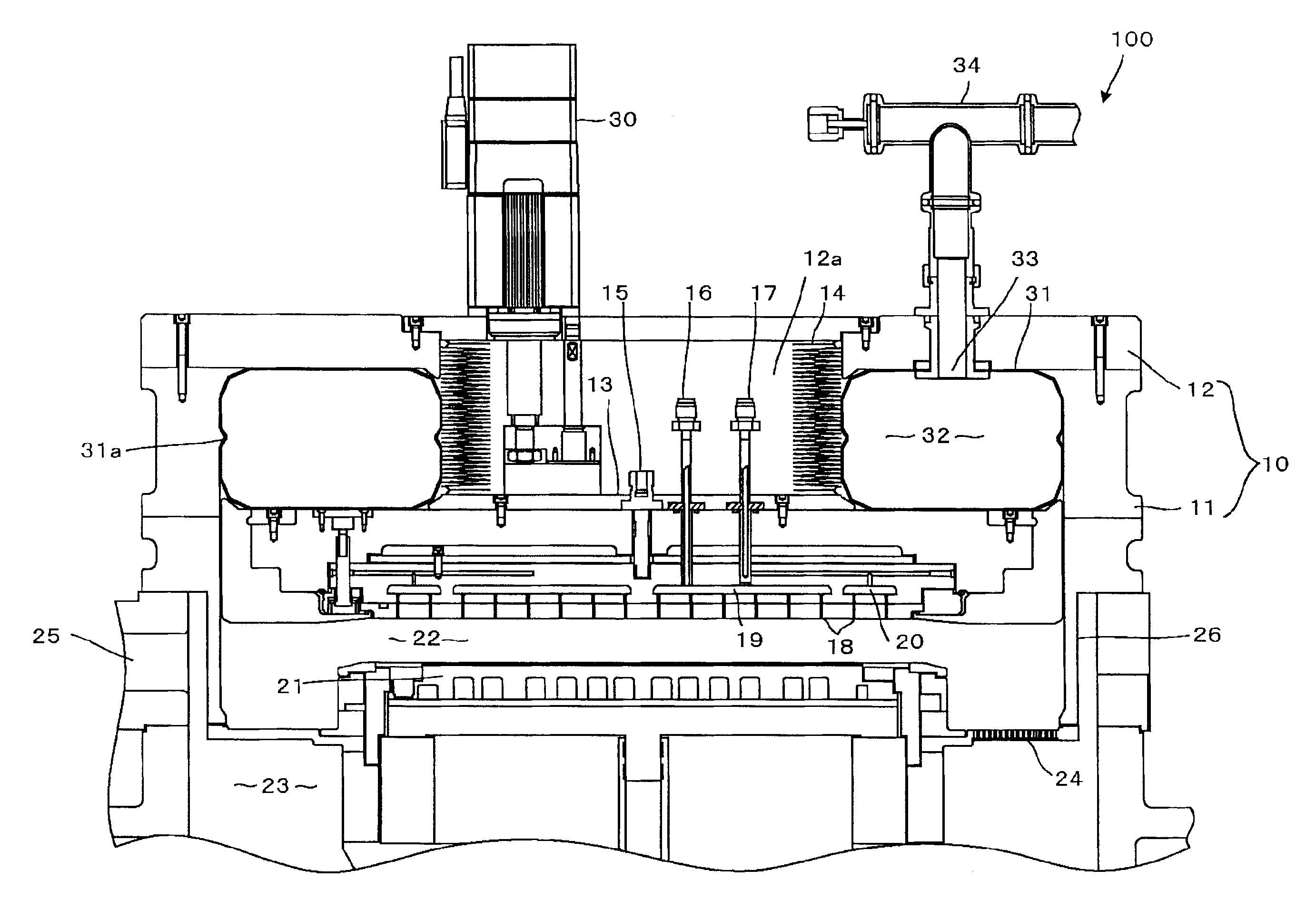
도 1은, 본 발명의 플라즈마 처리 장치의 제1 실시 형태에 따른 플라즈마 에칭 장치(100)의 구성을 개략적으로 나타내는 단면도이며, 도 2는, 도 1의 플라즈마 에칭 장치(100)의 요부 구성을 확대하여 개략적으로 나타내는 단면도이다. 본 실시 형태의 플라즈마 에칭 장치(100)는, 전극판이 상하로 평행하게 대향하여, 플라즈마 형성용 전원(도시하지 않음)이 접속된 용량 결합형 평행 평판 플라즈마 에칭 장치로서 그 주요부가 구성되어 있다.Fig. 1 is a cross-sectional view schematically showing the configuration of a
플라즈마 에칭 장치(100)는, 내부에 기판을 수용하여 처리하기 위한 원통 형상의 처리 챔버(10)를 구비하고 있다. 이 처리 챔버(10)는, 상부 개구를 갖고, 원통 용기 형상으로 형성된 처리 챔버 본체(11)와, 이 처리 챔버 본체(11)의 상부 개구를 기밀하게 폐색하는 덮개체(12)로 그 주요부가 구성되어 있다. 처리 챔버 본체(11) 및 덮개체(12)는, 예를 들면, 표면에 양극 산화 처리를 행한 알루미늄 등으로 구성되어 있다.The
덮개체(12)는, 중앙부에 원형의 개구(12a)를 갖는 환상의 형상으로 되어 있다. 또한, 처리 챔버(10) 내에는, 덮개체(12)의 하방에 위치하도록, 상부 전극으로서의 기능을 갖고, 전체 형상이 대략 원판 형상으로 형성된 샤워 헤드(13)가 설치되어 있다. 그리고, 덮개체(12)의 개구(12a)의 주위와 샤워 헤드(13)의 상면과의 사이에는, 이들 사이를 기밀하게 폐색하기 위한 원통 형상의 금속 벨로우즈(bellows; 14)가 설치되어 있다. The
상기와 같이, 중앙부에 원형의 개구(12a)를 갖는 환상의 덮개체(12)를 설치하고, 덮개체(12)와 샤워 헤드(13)의 상면과의 사이에 금속 벨로우즈(14)를 설치함으로써, 대기 중에 노출된 샤워 헤드(13)의 표면적을 작게 할 수 있어, 감압 분위기로 되는 처리 챔버(10) 내부와 외부(대기압)와의 기압차가 가해지는 부분의 면적을 작게 할 수 있어, 샤워 헤드(13)를 상하 이동시킬 때에 필요한 구동력을 보다 작게 할 수 있다.As described above, by providing the
대기 중 분위기에 노출된 샤워 헤드(13)의 상면의 부분에는, 샤워 헤드(13)를 상하 이동하기 위한 승강용 액츄에이터(30)의 구동축이 접속되어 있다. 승강용 액츄에이터(30)로서, 본 실시 형태에서는 전동(電動) 실린더를 이용하고 있다. 그리고, 복수의 승강용 액츄에이터(30)를 처리 챔버(10)의 둘레 방향을 따라서 등간격으로 설치한 다축 구동 방식으로 되어 있다. 이와 같이, 전동 실린더를 이용한 다축 구동 방식으로 함으로써, 예를 들면, 공기압 구동의 구동 기구로 한 경우에 비해 샤워 헤드(13)의 위치를 정밀도 좋게 제어할 수 있다. 또한, 다축 구동 방식으로 해도, 그 협조 제어(cooperative control)를 전기적으로 용이하게 행할 수 있다.The driving shaft of the
또한, 샤워 헤드(13)의 상면의 대략 중앙에는, 상부 전극 단자(15)가 설치되어 있고, 상부 전극 단자(15)의 측방에는, 제1 가스 도입부(16)와, 제2 가스 도입부(17)의 2개의 가스 도입부가 배치되어 있다. 상부 전극 단자(15)는, 도시하지 않은 고주파 전원 등의 고주파 전력 인가 장치에 접속되거나, 접지 전위에 접속된다.An
샤워 헤드(13)의 하면에는, 다수의 가스 토출공(18)이 배치되어 있다. 또한, 샤워 헤드(13)의 내부에는, 제1 가스 도입부(16)와 접속된 제1 가스 유로(19)와, 제2 가스 도입부(17)와 접속된 제2 가스 유로(20)가 설치되어 있다. 제1 가스 유로(19)는, 샤워 헤드(13)의 중앙 부분에 설치되어 있으며, 샤워 헤드(13)의 중앙 부분으로부터 처리 가스를 공급하기 위한 것이다. 한편, 제2 가스 유로(20)는, 샤워 헤드(13)의 주연부(周緣部)에 설치되어 있으며, 제2 가스 유로(20)는, 샤워 헤드(13)의 주연부로부터 처리 가스를 공급하기 위한 것이다.On the lower surface of the
처리 챔버(10) 내에는, 샤워 헤드(13)의 하부에, 샤워 헤드(13)의 하면과 대향하도록, 기판을 올려놓기 위한 재치대(21)가 설치되어 있다. 재치대(21)에는, 그 위에 기판을 정전 흡착하기 위한 도시하지 않은 정전 척(electrostatic chuck) 및, 올려놓여진 기판을 소정 온도로 온도 조절하기 위한 도시하지 않은 온도 조절용 매체 순환 유로가 설치되어 있다.In the
이 재치대(21)는, 하부 전극으로서의 기능을 갖고 있어, 상부 전극으로서의 샤워 헤드(13)와, 한 쌍의 대향 전극을 구성하고 있다. 재치대(21)에는, 도시하지 않은 고주파 전원 등의 고주파 전력 인가 장치가 접속되어 있어, 재치대(21)와 샤워 헤드(13)와의 사이는, 기판을 처리하기 위한 플라즈마가 발생되는 처리 공간(22)으로 되어 있다.The mounting table 21 has a function as a lower electrode and constitutes a
재치대(21)의 하방에는, 환상으로 형성된 배기 공간(23)이 형성되어 있어, 이 배기 공간(23)의 하방으로부터, 도시하지 않은 진공 펌프 등의 배기 장치에 의해 처리 챔버(10) 내를 소정의 진공도로 배기하도록 구성되어 있다. 또한, 재치대(21)의 주위에는, 처리 공간(22)과 배기 공간(23)을 나누기 위한 환상의 배플판(24)이 설치되어 있다.An
처리 공간(22)의 측방에 위치하는 처리 챔버(10)의 측벽부에는, 처리 챔버(10) 내에 기판을 반입·반출하기 위한 개구(25)가 배치되어 있다. 이 개구(25)에는, 게이트 밸브 등의 도시하지 않은 개폐 기구가 설치되어 있다. 또한, 처리 챔버(10)의 처리 공간(22)의 부분에는, 처리 챔버(10)의 내벽을 덮도록 실드 링(26)이 설치되어 있다.An
도 2에도 나타내는 바와 같이, 샤워 헤드(13)의 이면측(도 1, 2 중 상측)의, 샤워 헤드(13)와 덮개체(12)와의 사이에는, 이들 샤워 헤드(13)와 덮개체(12)와의 사이에 형성되는 공간(이면측 공간)을 폐색하도록, 격리 공간 형성 부재(31)가 설치되어 있다. 이 격리 공간 형성 부재(31)는, 샤워 헤드(13), 덮개체(12), 처리 챔버 본체(11)의 측벽, 금속 벨로우즈(14)에 의해 둘러싸인 공간의 형상에 맞추어 환상으로 형성되어 있다.2, the
또한, 본 실시 형태에서는, 격리 공간 형성 부재(31)는, 신축 자유로운 재료로 이루어져, 벌룬(balloon)과 같은 기능을 갖는 구성으로 되어 있고, 격리 공간 형성 부재(31)의 내측에는, 외측의 공간과는 격리된 격리 공간(32)이 형성되어 있다.In the present embodiment, the isolation
또한, 격리 공간 형성 부재(31)를 구성하는 재료로서는, 수지 등을 이용할 수 있고, 특히 탄성을 갖는 일래스터머(elastomer)(예를 들면, 실리콘 고무 또는 불소 고무 등)를 적합하게 이용할 수 있다. 또한, 격리 공간 형성 부재(31)를 구성하는 재료로서는, 절연성의 재료 또는 도전성 재료 중 어느 것을 이용해도 좋다.As the material forming the isolation
격리 공간 형성 부재(31)의 상면에는, 내부에 기체를 도입 및 배출하기 위한 도입·배출구(33)가 배치되어 있고, 이 도입·배출구(33)는, 기체 공급 배출 기구(34)가 접속되어 있다. 기체 공급 배출 기구(34)는, 도시하지 않은 기체 공급원 및 배기 기구에 접속되어 있다.An inlet /
격리 공간 형성 부재(31)는, 샤워 헤드(13)의 상하 이동에 수반하여 변형됨과 함께, 그 격리 공간(32)에, 기체 공급 배출 기구(34)로부터 불활성 가스 등의 기체가 도입, 배출됨으로써, 항상 부풀어 오른 상태로 되어 있어, 샤워 헤드(13), 덮개체(12), 처리 챔버 본체(11)의 측벽, 금속 벨로우즈(14)에 의해 둘러싸인 공간의 크기가 변화한 경우에도, 이 공간의 대략 전체를 차지하여, 이 공간이 격리 공간 형성 부재(31)에 의해 폐색된 상태를 유지할 수 있게 되어 있다.The
즉, 샤워 헤드(13)가 상하 이동한 경우에 있어서도, 격리 공간 형성 부재(31)에 의해, 샤워 헤드(13), 덮개체(12), 처리 챔버 본체(11)의 측벽, 금속 벨로우즈(14)에 의해 둘러싸인 공간이 항상 폐색되어, 격리 공간 형성 부재(31)의 외측에, 큰 공간이 형성되지 않도록 되어 있다. 또한, 도 3, 4에는, 도 1, 2에 나타낸 상태로부터 샤워 헤드(13)를 상승시켜, 처리 공간(22)을 확장시킨 상태를 나타내고 있다. 도 3, 4에 나타내는 상태에서는, 격리 공간 형성 부재(31)는, 그 높이 방향의 중간 부분에 배치된 접힘부(31a)가 내측으로 접혀진 상태로 되어 있다. 이와 같이, 격리 공간 형성 부재(31)가 접혀짐으로써, 샤워 헤드(13)를 상승시켜 용적이 작아진 이면측 공간 내에 극간(gap) 없이 배치되는 것이 가능해져 있다.That is, even when the
상기와 같이, 샤워 헤드(13)의 이면측의 이면측 공간이, 격리 공간 형성 부재(31)에 의해 폐색되어 있음으로써, 플라즈마 처리 중에 이 이면측 공간 내에서 이상 방전이 발생하는 것을 억제할 수 있다. 또한, 이상 방전에 기인하는 오염이 발생하는 것도 억제할 수 있다. 또한, 이면측 공간에 처리 가스가 유입되는 것을 억제할 수 있어, 이러한 이면측 공간으로의 처리 가스 유입에 기인하는 처리 공간(22)에 있어서의 플라즈마의 밀도의 저하나 이온의 양의 저감, 데포지션의 부착 등을 억제할 수 있다.As described above, since the space on the back side of the rear surface side of the
또한, 격리 공간 형성 부재(31)가 절연성 부재에 의해 구성되어 있는 경우는, 도체로 이루어지는 샤워 헤드(13), 덮개체(12), 처리 챔버 본체(11)의 측벽, 금속 벨로우즈(14)의 사이에 절연성 부재가 개재함으로써 이상 방전을 방지할 수 있다. 또한, 격리 공간 형성 부재(31)가 도전성 부재에 의해 구성되어 있는 경우는, 도체로 이루어지는 샤워 헤드(13), 덮개체(12), 처리 챔버 본체(11)의 측벽, 금속 벨로우즈(14)에 도전성의 격리 공간 형성 부재(31)가 접촉함으로써, 각부에 큰 전위차가 발생하는 것을 억제하여, 이에 따라 이상 방전을 방지할 수 있다.When the isolation
상기 구성의 플라즈마 에칭 장치(100)에 의해, 반도체 웨이퍼 등의 기판의 플라즈마 에칭을 행하는 경우, 처리 챔버(10)의 측벽에 형성된 개구(25)에 설치된 도시하지 않은 개폐 기구를 열고, 반송 로봇의 반송 아암 등에 의해 기판을, 개구(25)로부터 처리 챔버(10) 내로 반입하여, 재치대(21) 상에 올려놓고, 도시하지 않은 정전 척으로 흡착한다.When the plasma etching of the substrate such as the semiconductor wafer is performed by the
다음으로, 반송 로봇의 반송 아암 등을 처리 챔버(10) 내로부터 퇴피(退避)시켜 개구(25)를 닫고, 배기 공간(23)으로부터 도시하지 않은 배기 기구에 의해 배기하여, 처리 챔버(10) 내를 소정의 진공도로 한다. 그리고, 샤워 헤드(13)로부터 처리 챔버(10) 내에, 소정 유량의 소정의 처리 가스(에칭 가스)를 공급한다.Next, the transfer arm or the like of the transfer robot is retracted from the inside of the
그리고, 처리 챔버(10) 내의 압력이, 소정의 압력으로 유지된 후, 재치대(21)와 샤워 헤드(13)의 적어도 어느 한쪽, 예를 들면, 재치대(21)에만, 소정 주파수, 예를 들면 13.56MHz의 고주파 전력을 인가한다. 이에 따라, 상부 전극으로서의 샤워 헤드(13)와 하부 전극으로서의 재치대(21)와의 사이에 고주파 전계(electric field)가 발생하여, 에칭 가스가 해리되어 플라즈마화된다. 그리고, 이 플라즈마에 의해, 기판에 소정의 에칭 처리가 행해진다.After the pressure in the
이 에칭 처리시, 샤워 헤드(13)를 상하 이동시킴으로써, 샤워 헤드(13)와 재치대(21)와의 사이의 간격을, 에칭 처리에 최적인 간격으로 설정할 수 있기 때문에, 기판에 균일하고 양호한 에칭 처리를 행할 수 있다. 또한, 이 에칭 처리 중에, 샤워 헤드(13)의 이면측의 이면측 공간에서 이상 방전이 발생하는 것을 억제할 수 있어, 이상 방전에 의해 처리 공간(22)의 플라즈마 상태가 변화해 버리는 것을 억제할 수 있다. 또한, 이면측 공간에 데포지션물이 발생하는 것을 억제할 수 있기 때문에, 처리 중에 데포지션물이 박리되어 기판에 부착하여, 기판이 오염되는 것도 억제할 수 있다. 이에 따라, 양호한 에칭 처리를 안정적으로 행할 수 있다.Since the interval between the
그리고, 소정의 에칭 처리가 종료되면, 고주파 전력의 인가 및 처리 가스의 공급이 정지되고, 상기한 순서와는 반대의 순서로, 기판이 처리 챔버(10) 내로부터 반출된다.When the predetermined etching process is finished, the supply of the high-frequency power and the supply of the process gas are stopped, and the substrate is taken out from the
다음으로, 도 5∼8을 참조하여, 제2 실시 형태에 따른 플라즈마 에칭 장치(200)의 구성에 대해서 설명한다. 또한, 도 5, 6에 대하여, 도 7, 8은 샤워 헤드(13)를 보다 상승시킨 경우를 나타내고 있는 점은, 도 1∼4에 나타낸 전술한 제1 실시 형태의 경우와 동일하다.Next, the configuration of the
이 제2 실시 형태의 플라즈마 에칭 장치(200)에서는, 격리 공간 형성 부재(31)의 측면에, 내부에 기체를 도입 및 배출하기 위한 도입·배출구(33)가 배치되어 있고, 이 도입·배출구(33)에, 처리 챔버 본체(11) 측벽을 개재하여 기체 공급 배출 기구(34)가 접속되어 있다. 이와 같이, 격리 공간 형성 부재(31)의 도입·배출구(33)는, 상면에 한하지 않고, 측면에 설치해도 좋다. 또한, 제2 실시 형태의 플라즈마 에칭 장치(200)에 있어서, 다른 부분의 구성에 대해서는, 전술한 제1 실시 형태에 따른 플라즈마 에칭 장치(100)와 동일하게 구성되어 있기 때문에, 대응하는 부분에는, 동일한 부호를 붙여 중복된 설명은 생략한다.In the
또한, 본 발명은 상기 실시 형태로 한정되는 것이 아니며, 각종 변형이 가능한 것은 물론이다. 예를 들면, 상기 실시 형태에서는, 재치대(하부 전극)에 하나의 주파수의 고주파 전력을 공급하는 경우에 대해서 설명했지만, 하부 전극에 주파수가 상이한 복수의 고주파 전력을 인가하는 타입의 장치 등에 대해서도 동일하게 하여 적용할 수 있다.It is needless to say that the present invention is not limited to the above-described embodiment, and various modifications are possible. For example, in the above embodiment, a case has been described in which the high frequency power of one frequency is supplied to the mount (lower electrode). However, the same applies to the apparatus of the type in which a plurality of high frequency powers having different frequencies are applied to the lower electrode .
10 : 처리 챔버
11 : 처리 챔버 본체
12 : 덮개체
13 : 샤워 헤드(상부 전극)
14 : 금속 벨로우즈
21 : 재치대(하부 전극)
22 : 처리 공간
30 : 승강용 액츄에이터
31 : 격리 공간 형성 부재
32 : 격리 공간
33 : 도입·배출구
34 : 기체 공급 배출 기구
100, 200 : 플라즈마 에칭 장치10: Processing chamber
11: Processing chamber body
12:
13: showerhead (upper electrode)
14: Metal bellows
21: Mounting base (lower electrode)
22: Processing space
30: Lift actuator
31:
32: Isolation space
33: Introduction and discharge
34: gas supply / discharge mechanism
100, 200: Plasma etching apparatus
Claims (10)
상기 처리 챔버 내에 설치되어, 상기 기판을 올려놓기 위한 재치대를 겸한 하부 전극과,
상기 처리 챔버 내에 설치되어, 상기 하부 전극과 대향하여 상기 하부 전극과의 사이에 처리 공간을 형성함과 함께, 상기 하부 전극과 대향하는 대향면에 복수 형성된 가스 토출공으로부터 상기 기판을 향하여 처리 가스를 공급하는 샤워 헤드로서의 기능을 구비하고, 또한 상하 이동 가능하게 되어 상기 하부 전극과의 간격이 변경 가능하게 된 상부 전극과,
상기 상부 전극의 상측에 설치되어 상기 처리 챔버의 상부 개구를 기밀하게 폐색하는 덮개체와,
신축 자유로우며, 상기 덮개체와 상기 상부 전극의 상면과의 사이에 설치되는 벨로우즈와,
상기 상부 전극, 상기 덮개체, 상기 처리 챔버의 측벽 및 상기 벨로우즈에 의해 둘러싸인 환상의 공간에 설치되고, 그 안에 처리 챔버로부터 분리되는 격리 공간을 갖고, 접힘부를 가지며, 상기 격리 공간의 용적이 변동 가능하도록 당해 격리 공간에 또는 당해 격리 공간으로부터 기체를 도입 또는 배출하는 도입·배출구를 갖는 격리 공간 형성 부재로서, 상기 상부 전극이 상하 이동함에 따라 상기 환상의 공간의 크기가 변동할 때, 상기 격리 공간 형성 부재의 상기 격리 공간은 상기 환상의 공간을 채우도록 형성되는 격리 공간 형성 부재와,
상기 격리 공간 형성 부재의 상기 격리 공간에 또는 당해 격리 공간으로부터, 상기 도입·배출구를 통해 상기 기체를 공급 또는 배출하는 기체 공급 배출 기구와,
상기 상부 전극과 상기 하부 전극과의 사이에 고주파 전력을 공급하여 상기 처리 가스로부터 플라즈마를 발생시키는 고주파 전원을 구비한 것을 특징으로 하는 플라즈마 처리 장치.A processing chamber for accommodating a substrate and performing plasma processing;
A lower electrode provided in the processing chamber and also serving as a mount for mounting the substrate,
A processing space is formed in the processing chamber so as to be opposed to the lower electrode so as to be in contact with the lower electrode and a processing gas is supplied from the plurality of gas discharging holes formed on the opposing surface facing the lower electrode toward the substrate An upper electrode having a function as a showerhead to be supplied and capable of being moved up and down to change a distance from the lower electrode,
A cover body provided above the upper electrode to hermetically seal an upper opening of the processing chamber,
A bellows disposed between the lid body and the upper surface of the upper electrode,
Wherein the insulating space is provided in an annular space surrounded by the upper electrode, the lid body, the side wall of the processing chamber, and the bellows, and has an isolation space separated from the processing chamber therein, And an introduction / exhaust port for introducing or discharging gas from or into the isolation space, wherein when the size of the annular space varies as the upper electrode moves up and down, Wherein the isolation space of the member is formed to fill the annular space,
A gas supply / discharge mechanism for supplying or discharging the gas from / to the isolation space of the isolation space formation member through the introduction /
And a high frequency power source for generating a plasma from the process gas by supplying a high frequency power between the upper electrode and the lower electrode.
상기 격리 공간 형성 부재는 환상으로 형성되어 있는 것을 특징으로 하는 플라즈마 처리 장치.The method according to claim 1,
Wherein the isolation space forming member is formed in an annular shape.
상기 격리 공간 형성 부재가 엘라스토머(elastomer)로 구성되어 있는 것을 특징으로 하는 플라즈마 처리 장치.3. The method according to claim 1 or 2,
Wherein the isolation space forming member is made of an elastomer.
상기 격리 공간 형성 부재가, 실리콘 고무 또는 불소 고무로 구성되어 있는 것을 특징으로 하는 플라즈마 처리 장치.The method of claim 3,
Wherein the isolation space forming member is made of silicon rubber or fluorine rubber.
상기 기체 공급 배출 기구가 불활성 가스를 공급하는 것을 특징으로 하는 플라즈마 처리 장치.3. The method according to claim 1 or 2,
And the gas supply / discharge mechanism supplies an inert gas.
상기 격리 공간 형성 부재가 절연성 재료로 구성되어 있는 것을 특징으로 하는 플라즈마 처리 장치.3. The method according to claim 1 or 2,
Wherein the isolation space forming member is made of an insulating material.
상기 격리 공간 형성 부재가 도전성 재료로 구성되어 있는 것을 특징으로 하는 플라즈마 처리 장치.3. The method according to claim 1 or 2,
Wherein the isolation space forming member is made of a conductive material.
상기 도입·배출구가, 상기 격리 공간 형성 부재의 상면에 배치되어 있는 것을 특징으로 하는 플라즈마 처리 장치.3. The method according to claim 1 or 2,
And the introduction / exhaust port is disposed on the upper surface of the isolation space forming member.
상기 도입·배출구가, 상기 격리 공간 형성 부재의 측벽에 배치되어 있는 것을 특징으로 하는 플라즈마 처리 장치.3. The method according to claim 1 or 2,
Wherein the introduction / exhaust port is disposed on a side wall of the isolation space forming member.
Applications Claiming Priority (2)
| Application Number | Priority Date | Filing Date | Title |
|---|---|---|---|
| JPJP-P-2010-247362 | 2010-11-04 | ||
| JP2010247362A JP5700632B2 (en) | 2010-11-04 | 2010-11-04 | Plasma processing equipment |
Publications (2)
| Publication Number | Publication Date |
|---|---|
| KR20120049137A KR20120049137A (en) | 2012-05-16 |
| KR101892958B1 true KR101892958B1 (en) | 2018-08-29 |
Family
ID=46018494
Family Applications (1)
| Application Number | Title | Priority Date | Filing Date |
|---|---|---|---|
| KR1020110112588A Expired - Fee Related KR101892958B1 (en) | 2010-11-04 | 2011-11-01 | Plasma processing apparatus |
Country Status (5)
| Country | Link |
|---|---|
| US (1) | US9196461B2 (en) |
| JP (1) | JP5700632B2 (en) |
| KR (1) | KR101892958B1 (en) |
| CN (1) | CN102468155B (en) |
| TW (1) | TWI540943B (en) |
Families Citing this family (6)
| Publication number | Priority date | Publication date | Assignee | Title |
|---|---|---|---|---|
| US9449795B2 (en) * | 2013-02-28 | 2016-09-20 | Novellus Systems, Inc. | Ceramic showerhead with embedded RF electrode for capacitively coupled plasma reactor |
| TWI483283B (en) * | 2013-03-08 | 2015-05-01 | Archers Inc | Power transmission device and related plasma system |
| JP5840268B1 (en) * | 2014-08-25 | 2016-01-06 | 株式会社日立国際電気 | Substrate processing apparatus, semiconductor device manufacturing method, and recording medium |
| US10840065B2 (en) * | 2016-12-05 | 2020-11-17 | Toshiba Mitsubishi-Electric Industrial Systems Corporation | Active gas generation apparatus including a metal housing, first and second auxiliary members, and a housing contact |
| CN109321857B (en) * | 2018-08-29 | 2023-06-02 | 广州倬粤动力新能源有限公司 | Zinc wire processing method and equipment |
| JP7394661B2 (en) * | 2020-03-09 | 2023-12-08 | 東京エレクトロン株式会社 | Substrate processing equipment |
Citations (2)
| Publication number | Priority date | Publication date | Assignee | Title |
|---|---|---|---|---|
| US20100043975A1 (en) | 2008-06-11 | 2010-02-25 | Tokyo Electron Limited | Movable gas introduction structure and substrate processing apparatus having same |
| JP2010238961A (en) | 2009-03-31 | 2010-10-21 | Tokyo Electron Ltd | Gas flow path structure and substrate processing apparatus |
Family Cites Families (16)
| Publication number | Priority date | Publication date | Assignee | Title |
|---|---|---|---|---|
| JPS556409A (en) * | 1978-06-26 | 1980-01-17 | Hitachi Ltd | Plasma gas phase reactor |
| JPS5989759A (en) * | 1982-11-12 | 1984-05-24 | Hitachi Tokyo Electronics Co Ltd | Gaseous phase electrochemical reaction apparatus |
| JPS60114577A (en) * | 1983-11-26 | 1985-06-21 | Matsushita Electric Ind Co Ltd | chemical processing equipment |
| JPH07211647A (en) * | 1994-01-17 | 1995-08-11 | Hitachi Ltd | Gas phase chemical reactor |
| JP3536585B2 (en) * | 1997-04-25 | 2004-06-14 | 松下電器産業株式会社 | Workpiece plasma processing apparatus and plasma processing method |
| JP3476687B2 (en) | 1998-09-21 | 2003-12-10 | 東京エレクトロン株式会社 | Plasma processing equipment |
| JP2001148378A (en) * | 1999-11-22 | 2001-05-29 | Tokyo Electron Ltd | Plasma processing apparatus, cluster tool and plasma control method |
| JP2003181756A (en) * | 2001-12-19 | 2003-07-02 | Tokyo Seimitsu Co Ltd | Conditioner for wafer processing apparatus |
| JP4197884B2 (en) * | 2002-04-12 | 2008-12-17 | 仁 諏訪部 | Polishing equipment |
| JP4399219B2 (en) * | 2003-09-19 | 2010-01-13 | 東京エレクトロン株式会社 | Plasma processing apparatus and upper electrode unit |
| JP2004360028A (en) * | 2003-06-05 | 2004-12-24 | Ebara Corp | Plating facility |
| KR100614801B1 (en) * | 2004-07-05 | 2006-08-22 | 삼성전자주식회사 | Film Formation Method of Semiconductor Device |
| WO2006137541A1 (en) * | 2005-06-23 | 2006-12-28 | Tokyo Electron Limited | Constitutional member for semiconductor processing apparatus and method for producing same |
| KR101006848B1 (en) * | 2008-05-28 | 2011-01-14 | 주식회사 코미코 | Substrate support device and substrate processing apparatus including same |
| JP2010021510A (en) * | 2008-06-13 | 2010-01-28 | Canon Anelva Corp | Substrate support device and plasma processing apparatus |
| JP5643528B2 (en) * | 2009-03-30 | 2014-12-17 | 東京エレクトロン株式会社 | Substrate processing equipment |
-
2010
- 2010-11-04 JP JP2010247362A patent/JP5700632B2/en not_active Expired - Fee Related
-
2011
- 2011-11-01 KR KR1020110112588A patent/KR101892958B1/en not_active Expired - Fee Related
- 2011-11-01 TW TW100139856A patent/TWI540943B/en active
- 2011-11-02 US US13/287,484 patent/US9196461B2/en not_active Expired - Fee Related
- 2011-11-03 CN CN201110345886.XA patent/CN102468155B/en not_active Expired - Fee Related
Patent Citations (2)
| Publication number | Priority date | Publication date | Assignee | Title |
|---|---|---|---|---|
| US20100043975A1 (en) | 2008-06-11 | 2010-02-25 | Tokyo Electron Limited | Movable gas introduction structure and substrate processing apparatus having same |
| JP2010238961A (en) | 2009-03-31 | 2010-10-21 | Tokyo Electron Ltd | Gas flow path structure and substrate processing apparatus |
Also Published As
| Publication number | Publication date |
|---|---|
| TWI540943B (en) | 2016-07-01 |
| TW201234935A (en) | 2012-08-16 |
| JP2012099715A (en) | 2012-05-24 |
| KR20120049137A (en) | 2012-05-16 |
| JP5700632B2 (en) | 2015-04-15 |
| US20120111501A1 (en) | 2012-05-10 |
| US9196461B2 (en) | 2015-11-24 |
| CN102468155B (en) | 2014-06-25 |
| CN102468155A (en) | 2012-05-23 |
Similar Documents
| Publication | Publication Date | Title |
|---|---|---|
| CN102142357B (en) | Plasma processing apparatus | |
| JP5188385B2 (en) | Plasma processing apparatus and method of operating plasma processing apparatus | |
| KR100624273B1 (en) | Plasma processing apparatus | |
| JP6435135B2 (en) | Plasma processing equipment | |
| KR101850355B1 (en) | Plasma processing apparatus | |
| CN102254847B (en) | Plamsa processing apparatus | |
| KR101672856B1 (en) | Plasma processing apparatus | |
| KR101892958B1 (en) | Plasma processing apparatus | |
| KR20190019965A (en) | Plasma processing apparatus | |
| US11621151B2 (en) | Upper electrode and plasma processing apparatus | |
| TWI882627B (en) | Plasma source for semiconductor processing | |
| US20220084798A1 (en) | Plasma processing apparatus and electrode structure | |
| JP2020115519A (en) | Mounting table and substrate processing device | |
| US20250104978A1 (en) | Ring assembly and substrate processing apparatus comprising the same |
Legal Events
| Date | Code | Title | Description |
|---|---|---|---|
| PA0109 | Patent application |
St.27 status event code: A-0-1-A10-A12-nap-PA0109 |
|
| PG1501 | Laying open of application |
St.27 status event code: A-1-1-Q10-Q12-nap-PG1501 |
|
| E13-X000 | Pre-grant limitation requested |
St.27 status event code: A-2-3-E10-E13-lim-X000 |
|
| P11-X000 | Amendment of application requested |
St.27 status event code: A-2-2-P10-P11-nap-X000 |
|
| P13-X000 | Application amended |
St.27 status event code: A-2-2-P10-P13-nap-X000 |
|
| PA0201 | Request for examination |
St.27 status event code: A-1-2-D10-D11-exm-PA0201 |
|
| P11-X000 | Amendment of application requested |
St.27 status event code: A-2-2-P10-P11-nap-X000 |
|
| P13-X000 | Application amended |
St.27 status event code: A-2-2-P10-P13-nap-X000 |
|
| E902 | Notification of reason for refusal | ||
| PE0902 | Notice of grounds for rejection |
St.27 status event code: A-1-2-D10-D21-exm-PE0902 |
|
| P11-X000 | Amendment of application requested |
St.27 status event code: A-2-2-P10-P11-nap-X000 |
|
| P13-X000 | Application amended |
St.27 status event code: A-2-2-P10-P13-nap-X000 |
|
| E701 | Decision to grant or registration of patent right | ||
| PE0701 | Decision of registration |
St.27 status event code: A-1-2-D10-D22-exm-PE0701 |
|
| GRNT | Written decision to grant | ||
| PR0701 | Registration of establishment |
St.27 status event code: A-2-4-F10-F11-exm-PR0701 |
|
| PR1002 | Payment of registration fee |
St.27 status event code: A-2-2-U10-U11-oth-PR1002 Fee payment year number: 1 |
|
| PG1601 | Publication of registration |
St.27 status event code: A-4-4-Q10-Q13-nap-PG1601 |
|
| PR1001 | Payment of annual fee |
St.27 status event code: A-4-4-U10-U11-oth-PR1001 Fee payment year number: 4 |
|
| PR1001 | Payment of annual fee |
St.27 status event code: A-4-4-U10-U11-oth-PR1001 Fee payment year number: 5 |
|
| PC1903 | Unpaid annual fee |
St.27 status event code: A-4-4-U10-U13-oth-PC1903 Not in force date: 20230824 Payment event data comment text: Termination Category : DEFAULT_OF_REGISTRATION_FEE |
|
| P22-X000 | Classification modified |
St.27 status event code: A-4-4-P10-P22-nap-X000 |
|
| PC1903 | Unpaid annual fee |
St.27 status event code: N-4-6-H10-H13-oth-PC1903 Ip right cessation event data comment text: Termination Category : DEFAULT_OF_REGISTRATION_FEE Not in force date: 20230824 |
|
| P22-X000 | Classification modified |
St.27 status event code: A-4-4-P10-P22-nap-X000 |