KR101867999B1 - Method of forming III-V group material layer, semiconductor device comprising III-V group material layer and method of manufacturing the same - Google Patents
Method of forming III-V group material layer, semiconductor device comprising III-V group material layer and method of manufacturing the same Download PDFInfo
- Publication number
- KR101867999B1 KR101867999B1 KR1020110112499A KR20110112499A KR101867999B1 KR 101867999 B1 KR101867999 B1 KR 101867999B1 KR 1020110112499 A KR1020110112499 A KR 1020110112499A KR 20110112499 A KR20110112499 A KR 20110112499A KR 101867999 B1 KR101867999 B1 KR 101867999B1
- Authority
- KR
- South Korea
- Prior art keywords
- iii
- insulating layer
- layer
- material layer
- substrate
- Prior art date
- Legal status (The legal status is an assumption and is not a legal conclusion. Google has not performed a legal analysis and makes no representation as to the accuracy of the status listed.)
- Active
Links
Images


Classifications
-
- H—ELECTRICITY
- H10—SEMICONDUCTOR DEVICES; ELECTRIC SOLID-STATE DEVICES NOT OTHERWISE PROVIDED FOR
- H10D—INORGANIC ELECTRIC SEMICONDUCTOR DEVICES
- H10D64/00—Electrodes of devices having potential barriers
- H10D64/20—Electrodes characterised by their shapes, relative sizes or dispositions
- H10D64/27—Electrodes not carrying the current to be rectified, amplified, oscillated or switched, e.g. gates
- H10D64/311—Gate electrodes for field-effect devices
- H10D64/411—Gate electrodes for field-effect devices for FETs
- H10D64/511—Gate electrodes for field-effect devices for FETs for IGFETs
- H10D64/517—Gate electrodes for field-effect devices for FETs for IGFETs characterised by the conducting layers
- H10D64/518—Gate electrodes for field-effect devices for FETs for IGFETs characterised by the conducting layers characterised by their lengths or sectional shapes
-
- H—ELECTRICITY
- H10—SEMICONDUCTOR DEVICES; ELECTRIC SOLID-STATE DEVICES NOT OTHERWISE PROVIDED FOR
- H10D—INORGANIC ELECTRIC SEMICONDUCTOR DEVICES
- H10D30/00—Field-effect transistors [FET]
- H10D30/40—FETs having zero-dimensional [0D], one-dimensional [1D] or two-dimensional [2D] charge carrier gas channels
- H10D30/47—FETs having zero-dimensional [0D], one-dimensional [1D] or two-dimensional [2D] charge carrier gas channels having 2D charge carrier gas channels, e.g. nanoribbon FETs or high electron mobility transistors [HEMT]
- H10D30/471—High electron mobility transistors [HEMT] or high hole mobility transistors [HHMT]
- H10D30/475—High electron mobility transistors [HEMT] or high hole mobility transistors [HHMT] having wider bandgap layer formed on top of lower bandgap active layer, e.g. undoped barrier HEMTs such as i-AlGaN/GaN HEMTs
- H10D30/4755—High electron mobility transistors [HEMT] or high hole mobility transistors [HHMT] having wider bandgap layer formed on top of lower bandgap active layer, e.g. undoped barrier HEMTs such as i-AlGaN/GaN HEMTs having wide bandgap charge-carrier supplying layers, e.g. modulation doped HEMTs such as n-AlGaAs/GaAs HEMTs
-
- H—ELECTRICITY
- H10—SEMICONDUCTOR DEVICES; ELECTRIC SOLID-STATE DEVICES NOT OTHERWISE PROVIDED FOR
- H10D—INORGANIC ELECTRIC SEMICONDUCTOR DEVICES
- H10D62/00—Semiconductor bodies, or regions thereof, of devices having potential barriers
- H10D62/10—Shapes, relative sizes or dispositions of the regions of the semiconductor bodies; Shapes of the semiconductor bodies
- H10D62/17—Semiconductor regions connected to electrodes not carrying current to be rectified, amplified or switched, e.g. channel regions
- H10D62/213—Channel regions of field-effect devices
- H10D62/221—Channel regions of field-effect devices of FETs
- H10D62/235—Channel regions of field-effect devices of FETs of IGFETs
-
- H—ELECTRICITY
- H10—SEMICONDUCTOR DEVICES; ELECTRIC SOLID-STATE DEVICES NOT OTHERWISE PROVIDED FOR
- H10D—INORGANIC ELECTRIC SEMICONDUCTOR DEVICES
- H10D62/00—Semiconductor bodies, or regions thereof, of devices having potential barriers
- H10D62/80—Semiconductor bodies, or regions thereof, of devices having potential barriers characterised by the materials
- H10D62/85—Semiconductor bodies, or regions thereof, of devices having potential barriers characterised by the materials being Group III-V materials, e.g. GaAs
Landscapes
- Insulated Gate Type Field-Effect Transistor (AREA)
- Thin Film Transistor (AREA)
- Junction Field-Effect Transistors (AREA)
Abstract
III-V족 물질층을 형성하는 방법, III-V족 물질층을 포함하는 반도체 소자 및 그 제조방법에 관해 개시되어 있다. 본 발명의 일 실시예에 의한 반도체 소자는 기판, 상기 기판 상에 형성된 III-V족 채널층, 상기 채널층 상에 형성된 게이트 절연층, 상기 게이트 절연층 상에 형성된 게이트 전극, 상기 게이트 전극과 이격된 소스 및 드레인 전극을 포함하고, 상기 III-V족 채널층의 하단부 둘레에 공극이 존재한다. 상기 III-V족 채널층은 2원계 물질, 3원계 물질 또는 4원계 물질을 포함할 수 있다.A method of forming a III-V material layer, a semiconductor device including a III-V material layer, and a manufacturing method thereof. A semiconductor device according to an embodiment of the present invention includes a substrate, a III-V channel layer formed on the substrate, a gate insulating layer formed on the channel layer, a gate electrode formed on the gate insulating layer, Source and drain electrodes, and voids are present around the lower end of the III-V channel layer. The III-V channel layer may include a binary material, a ternary material, or a quaternary material.
Description
본 발명의 일 실시예는 반도체 소자 및 그 제조방법과 관련된 것으로써, 보다 자세하게는 III-V족 물질층을 형성하는 방법, III-V족 물질층을 포함하는 반도체 소자 및 그 제조방법에 관한 것이다.An embodiment of the present invention relates to a semiconductor device and a method of manufacturing the same, and more particularly to a method of forming a III-V material layer, a semiconductor device including a III-V material layer, and a manufacturing method thereof .
반도체 소자의 집적도가 높아지면서 반도체 소자를 구성하는 요소들의 사이즈가 작아지고, 요소들 사이의 간격도 좁아진다. 예컨대, 실리콘(Si) 기반 트랜지스터의 경우, 소스, 드레인 및 게이트의 사이즈가 작아질 뿐 아니라, 소스, 드레인 및 게이트 사이의 간격도 좁아진다. 게이트 사이즈가 작아지면서 채널길이가 짧아지고, 이에 따른 짧은 채널 효과(short channel effect)가 발생되어 트랜지스터의 특성이 저하된다. 트랜지스터의 게이트 사이즈 한계를 극복하기 위한 대안으로 트랜지스터의 채널 물질을 III-V 족 물질로 대체하는 방법이 제안되고 있다. 그러나 III-V 물질과 실리콘(Si) 사이의 결정 상수 차이와 열전도도 차이로 인해 두 물질의 계면에 많은 결함을 발생되고, 이러한 결함들 때문에 디바이스 응용에 한계가 있다.As the degree of integration of the semiconductor elements increases, the sizes of the elements constituting the semiconductor elements become smaller, and the interval between the elements becomes narrower. For example, in the case of a silicon (Si) -based transistor, not only the sizes of the source, drain and gate are reduced, but also the distance between the source, the drain and the gate is narrowed. As the gate size is reduced, the channel length is shortened, and a short channel effect is generated thereby to degrade the characteristics of the transistor. As an alternative to overcoming the gate size limitations of transistors, a method has been proposed to replace the channel material of a transistor with a III-V material. However, due to the difference in crystal constant and the difference in thermal conductivity between the III-V material and silicon (Si), a large number of defects are generated at the interfaces of the two materials.
본 발명의 일 실시예는 결함을 포함하지 않거나 결함을 크게 줄인 III-V족 물질층을 포함하는 반도체 소자를 제공한다.One embodiment of the present invention provides a semiconductor device comprising a layer of a III-V material that does not contain defects or significantly reduces defects.
본 발명의 일 실시예는 이러한 반도체 소자의 제조방법을 제공한다.One embodiment of the present invention provides a method of manufacturing such a semiconductor device.
본 발명의 일 실시예는 상기 반도체 소자에 사용되는 III-V족 물질층의 형성방법을 제공한다.One embodiment of the present invention provides a method of forming a III-V material layer for use in the semiconductor device.
본 발명의 일 실시예에 의한 III-V족 물질을 포함하는 반도체 소자는 기판, 상기 기판 상에 형성된 III-V족 채널층, 상기 채널층 상에 형성된 게이트 절연층, 상기 게이트 절연층 상에 형성된 게이트 전극, 상기 게이트 전극과 이격된 소스 및 드레인 전극을 포함하고, 상기 III-V족 채널층의 하단부 둘레에 공극이 존재한다.A semiconductor device including a III-V material according to an embodiment of the present invention includes a substrate, a III-V channel layer formed on the substrate, a gate insulating layer formed on the channel layer, A gate electrode, and source and drain electrodes spaced apart from the gate electrode, wherein a void is present around the lower end of the III-V channel layer.
상기 III-V족 채널층은 2원계 물질, 3원계 물질 또는 4원계 물질을 포함할 수 있다.The III-V channel layer may include a binary material, a ternary material, or a quaternary material.
상기 III-V족 채널층 주변에 상기 III-V족 채널층보다 낮고, 일부는 III-V족 채널층와 이격된 절연층이 존재할 수 있다.An insulating layer may be present around the III-V channel layer, which is lower than the III-V channel layer and partly apart from the III-V channel layer.
상기 절연층은 순차적으로 적층된 제1 및 제2 절연층이고, 상기 제1 절연층은 상기 III-V족 채널층과 이격되어 있다.The insulating layer is a first insulating layer and a second insulating layer sequentially stacked, and the first insulating layer is spaced apart from the III-V channel layer.
상기 제1 및 제2 절연층은 실리콘 산화물, 알루미늄 산화물 또는 실리콘 질화막일 수 있다.The first and second insulating layers may be silicon oxide, aluminum oxide, or silicon nitride.
상기 제2 절연층은 실리콘 질화물, 알루미늄 산화물 또는 실리콘 질화막일 수 있다.The second insulating layer may be silicon nitride, aluminum oxide, or silicon nitride.
본 발명의 일 실시예에 의한 III-V족 물질을 포함하는 반도체 소자의 제조방법은 기판 상에 제1 및 제2 절연층을 형성하고, 상기 제2 절연층에 상기 제1 절연층의 상부면의 일부가 노출되는 홈을 형성하고, 상기 제1 절연층의 노출된 부분을 제거하여 상기 기판을 노출시키고, 상기 제2 절연층 아래에 언더 컷을 형성하고, 상기 언더 컷 사이의 상기 기판 상에 상기 홈을 채우는 III-V족 물질층을 선택적으로 성장시키고, 상기 제2 절연층의 일부를 제거하여 상기 III-V족 물질층의 측면 일부를 노출시키고, 상기 III-V족 물질층의 상부면과 노출된 측면을 덮는 게이트 절연층을 형성하고, 상기 게이트 절연층 상에 게이트 전극을 형성하며, 상기 III-V족 물질층 상에 상기 게이트 전극과 이격되는 소스 및 드레인 전극을 형성하는 과정을 포함한다.A method of fabricating a semiconductor device including a III-V material according to an embodiment of the present invention includes forming a first and a second insulating layer on a substrate, forming a second insulating layer on the upper surface of the first insulating layer Forming a groove in which a part of the first insulating layer is exposed, exposing the substrate by removing an exposed portion of the first insulating layer, forming an undercut under the second insulating layer, And selectively removing a portion of the III-V material layer to expose a side portion of the III-V material layer; and removing a portion of the III-V material layer And forming a gate insulating layer on the exposed side surface, forming a gate electrode on the gate insulating layer, and forming source and drain electrodes spaced apart from the gate electrode on the III-V material layer do.
이러한 제조방법에서, 상기 제1 및 제2 절연층은 실리콘 산화물과 실리콘 질화물 및 알루미늄 산화물 중 선택된 서로 다른 물질로 형성할 수 있다.In this manufacturing method, the first and second insulating layers may be formed of different materials selected from silicon oxide, silicon nitride, and aluminum oxide.
상기 III-V족 물질층은 적어도 하나의 III족 원소와 적어도 하나의 V족 원소를 포함하는, 2원계, 3원계 또는 4원계 물질로 형성할 수 있다.The III-V material layer may be formed of a binary, ternary, or quaternary material including at least one Group III element and at least one Group V element.
상기 III-V족 물질층이 형성되는 위치에서 상기 제1 및 제2 절연층으로 이루어진 절연층의 종횡비는 0.1~4일 수 있다.The aspect ratio of the insulating layer composed of the first and second insulating layers at a position where the III-V material layer is formed may be 0.1 to 4.
상기 언더 컷 사이의 상기 기판 상에 상기 홈을 채우는 III-V족 물질층을 선택적으로 성장시키는 과정은, 상기 언더 컷 사이의 상기 기판 상에 상기 홈을 채우고, 상기 제2 절연층 보다 높게 III-V족 물질층을 성장시키고, 상기 III-V족 물질층을 연마하여 상기 III-V족 물질층의 높이를 상기 제2 절연층의 높이로 낮추는 과정을 더 포함한다.Wherein the step of selectively growing the III-V material layer filling the grooves on the substrate between the undercuts comprises filling the grooves on the substrate between the undercuts and selectively etching the III- V material layer and polishing the III-V material layer to lower the height of the III-V material layer to a height of the second insulating layer.
본 발명의 일 실시예에 의한 III-V족 물질층의 형성방법은 기판 상에 제1 및 제2 절연층을 형성하고, 상기 제2 절연층에 상기 제1 절연층의 상부면의 일부가 노출되는 홈을 형성하고, 상기 제1 절연층의 노출된 부분을 제거하여 상기 기판을 노출시키고, 상기 제2 절연층 아래에 언더 컷을 형성하고, 상기 언더 컷 사이의 상기 기판 상에 상기 홈을 채우는 III-V족 물질층을 선택적으로 성장시키는 과정을 포함한다.A method of forming a III-V material layer according to an embodiment of the present invention includes forming a first and a second insulating layer on a substrate and exposing a portion of the upper surface of the first insulating layer to the second insulating layer Forming an undercut on the substrate between the undercuts, forming a groove in the first insulating layer, exposing the substrate by removing an exposed portion of the first insulating layer, forming an undercut below the second insulating layer, Lt; RTI ID = 0.0 > III-V < / RTI >
이러한 형성방법은 상기 제2 절연층의 일부를 제거하여 상기 III-V족 물질층의 측면 일부를 노출시키는 과정을 더 포함할 수 있다.The forming method may further include removing a portion of the second insulating layer to expose a side surface of the III-V material layer.
본 발명의 일 실시예에 의한 반도체 소자는 실리콘 기판의 선택된 영역에 III-V족 물질, 예컨대 III-V족 화합물 반도체를 성장시키는 과정에서 성장되는 III-V족 물질의 하단부 주변에 만들어진 공극(empty space)을 포함한다. 이러한 공극에 의해 III-V족 물질의 성장 과정에서 III-V족 물질과 실리콘 기판 사이의 격자상수 및 열 전도율 차이로 인해 III-V족 물질이 받은 스트레스가 완화된다. 이에 따라 III-V족 물질의 성장시에 형성되는 결함은 대부분 III-V족 물질의 하단부에 존재하게 되어 III-V족 물질의 하단부 위쪽 부분은 결함을 거의 포함하지 않는 고 품질의 물질로 성장될 수 있다. 이렇게 성장된 III-V족 물질을 채널로 사용하거나 III-V족 화합물 반도체 기판으로 사용함으로써, 실리콘(Si)을 기반으로 한 반도체 소자보다 전기적 및 동작 특성이 향상된 반도체 소자를 얻을 수 있다. A semiconductor device according to an embodiment of the present invention may include a space formed around a lower portion of a III-V material grown in a process of growing a III-V material, for example, a III-V compound semiconductor, space. These pores mitigate the stresses experienced by III-V materials due to differences in lattice constant and thermal conductivity between III-V materials and silicon substrates during the growth of III-V materials. Thus, most of the defects formed during the growth of the III-V material are present at the bottom of the III-V material, so that the upper portion of the III-V material is grown to a high quality material that contains few defects . By using the grown III-V material as a channel or as a III-V compound semiconductor substrate, it is possible to obtain a semiconductor device having improved electrical and operational characteristics as compared with a semiconductor device based on silicon (Si).
도 1은 본 발명의 일 실시예에 의한 III-V족 물질 채널층을 포함하는 반도체 소자의 단면도이다.
도 2는 도 1을 2-2’방향으로 절개한 단면도이다.
도 3 내지 도 9는 본 발명의 일 실시예에 의한 III-V족 물질 채널층을 포함하는 반도체 소자의 제조 방법을 단계별로 나타낸 단면도들이다.1 is a cross-sectional view of a semiconductor device including a III-V material channel layer according to an embodiment of the present invention.
FIG. 2 is a cross-sectional view of FIG. 1 taken along line 2-2 '.
FIGS. 3 to 9 are cross-sectional views illustrating a method of manufacturing a semiconductor device including a III-V material channel layer according to an embodiment of the present invention.
이하, 본 발명의 일 실시예에 의한 III-V족 물질층을 형성하는 방법, III-V족 물질층을 포함하는 반도체 소자 및 그 제조방법을 첨부된 도면들을 참조하여 상세하게 설명한다. 이 과정에서 도면에 도시된 층이나 영역들의 두께는 명세서의 명확성을 위해 과장되게 도시된 것이다.Hereinafter, a method of forming a III-V material layer according to an embodiment of the present invention, a semiconductor device including a III-V material layer, and a manufacturing method thereof will be described in detail with reference to the accompanying drawings. In this process, the thicknesses of the layers or regions shown in the figures are exaggerated for clarity of the description.
III-V족 물질층을 형성하는 방법은 반도체 소자의 제조 방법에서 함께 설명한다.The method of forming the III-V material layer is described together in the method of manufacturing a semiconductor device.
먼저, 본 발명의 일 실시예에 의한 III-V족 물질층을 포함하는 반도체 소자에 대해 설명한다.First, a semiconductor device including a III-V material layer according to an embodiment of the present invention will be described.
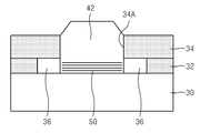
도 1을 참조하면, 기판(30)의 일부 영역 상에 III-V족 물질층(42)이 존재한다. 기판(30)은, 예를 들면 실리콘 기판일 수 있다. III-V족 물질층(42)은 트랜지스터의 채널층일 수 있다. III-V족 물질층(42)은, 예를 들면 III-V족 화합물 반도체층일 수 있다. 상기 III-V족 화합물 반도체층은, 예를 들면 2원계 물질, 3원계 물질 또는 4원계 물질을 포함할 수 있다. 상기 2원계 물질은, 예를 들면 GaAs, GaP, InP, InAs, GaSb, InSb, AlP, AlAs 또는 AlSb일 수 있다. 상기 3원계와 4원계 물질은, 예를 들면 In, Ga 및 Al 중 적어도 하나의 III족 원소와 As, P 및 Sb 중 적어도 하나의 V족 원소를 포함할 수 있다. III-V족 물질층(42) 양쪽에 순차적으로 적층된 제1 및 제2 절연층(32, 34)이 형성되어 있다. 제1 절연층(32) 상에 형성된 제2 절연층(34)의 상부면은 III-V족 물질층(42)의 상부면 보다 낮다. 제2 절연층(34)은 III-V족 물질층(42)의 측면에 접촉된다. 그러나 제1 절연층(32)은 III-V족 물질층(42)과 접촉되지 않는다. 곧, 제1 절연층(32)은 III-V족 물질층(42)과 이격되어 있다. 이에 따라 제1 절연층(32)과 III-V족 물질층(42) 사이에는 공극 또는 빈공간(empty space)(36)이 존재한다. 공극(36)의 부피는 본 발명의 일 실시예에 의한 반도체 소자의 제조 과정에서 조절할 수 있다. 이러한 공극(36)이 존재함으로써, III-V족 물질층(42)이 성장될 때, 기판(30)과의 격자상수 및 열 전도율 차이 등으로 인해 III-V족 물질층(42)이 받을 수 있는 스트레스를 완화시킬 수 있다. 또한, 공극(36)이 존재함으로 인해, III-V족 물질층(42)이 성장될 때 형성되는 결함(50)은 III-V족 물질층(42)의 하단부로 제한될 수 있다. 제1 및 제2 절연층(32, 34)은 식각 선택비가 서로 다른 물질일 수 있다. 제1 절연층(32)은, 예를 들면 실리콘 산화물, 알루미늄 산화물 또는 실리콘 질화물로 형성된 것일 수 있다. 제2 절연층(34)은, 예를 들면 실리콘 질화물, 알루미늄 산화물 또는 실리콘 질화물로 형성된 것일 수 있다.Referring to FIG. 1, there is a III-
도면에서 결함(50)은 직선으로 도시하였으나, 이는 단순히 상징적인 것이다. 결함(50)은 사선 방향으로 존재할 수도 있고, 비 직선 형태로 존재할 수도 있다. III-V족 물질층(42)의 돌출된 부분, 곧 제2 절연층(34)보다 높은 부분은 결함(50)을 포함하지 않는다. III-V족 물질층(42)의 돌출된 부분의 상부면과 측면 상에 게이트 절연층(56)이 존재한다. 게이트 절연층(56)은, 예를 들면 실리콘 산화물일 수 있다. 게이트 절연층(56) 상에 게이트 전극(58)이 존재한다. 게이트 전극(58)은 III-V족 물질층(42)의 상기 돌출된 부분을 덮는다. 따라서 도 1의 반도체 소자는 핀형 트랜지스터가 된다.In the drawing, the
도 2는 도 1을 2-2’방향으로 절개한 단면을 보여준다.FIG. 2 shows a cross section of FIG. 1 taken along line 2-2 '.
도 2를 참조하면, III-V족 물질층(42) 상에 소스 및 드레인 전극(62, 64)이 이격되게 구비되어 있다. 소스 전극(62)과 드레인 전극(64) 사이의 III-V족 물질층(42) 상에 게이트 절연층(56)이 구비되고, 게이트 절연층(56) 상에 게이트 전극(58)이 존재한다. 소스 및 드레인 전극(62, 64)은 이격되어 있다. 소스 및 드레인 전극(62, 64) 사이에 게이트 절연층(56)과 게이트 전극(58)이 존재한다.Referring to FIG. 2, source and
다음에는 본 발명의 일 실시예에 의한 반도체 소자의 제조방법을 도 3 내지 도 9를 참조하여 설명한다.Next, a method of manufacturing a semiconductor device according to an embodiment of the present invention will be described with reference to FIGS. 3 to 9. FIG.
도 3을 참조하면, 기판(30) 상에 제1 절연층(32)을 형성한다. 제1 절연층(32)은, 예를 들면 실리콘 산화물로 형성할 수 있다. 제1 절연층(32) 상에 제2 절연층(34)을 형성한다. 제2 절연층(34)은 제1 절연층(32)에 대해 식각 선택비가 다른 절연 물질일 수 있다. 제2 절연층(34)은, 예를 들면 실리콘 질화물로 형성할 수 있다. 제2 절연층(34) 상에 제2 절연층(34)의 일부 영역을 한정하는 마스크(M1)를 형성한다. 마스크(M1)의 형성으로 후속 공정에서 III-V족 물질층이 형성될 영역이 정해질 수 있다. 마스크(M1)는, 예를 들면 감광막 패턴일 수 있다. 마스크(M1) 형성 후, 제2 절연층(34)의 노출된 부분을 제거한다. 제2 절연층(34)의 노출된 부분의 제거는, 예를 들면 이방성 건식 식각 방법으로 수행할 수 있고, 제1 절연층(32)이 노출될 때까지 실시할 수 있다. 제2 절연층(34)의 노출된 부분이 제거되면서 도 4에 도시한 바와 같이, 제2 절연층(34)의 노출된 부분 아래의 제1 절연층(32)이 노출된다.Referring to FIG. 3, a first insulating
도 5에서 제1 및 제2 절연층(32, 34)으로 이루어진 절연층의 종횡비(H1/W1)는 0.1 이상일 수 있는데, 예를 들면 0.1~4 정도일 수 있다.In FIG. 5, the aspect ratio H1 / W1 of the insulating layer composed of the first and second insulating
다음, 도 6을 참조하면, 기판(30)의 상부면의 노출된 영역 상에 III-V족 물질층(42)을 형성한다. III-V족 물질층(42)은 제2 절연층(34)의 홈(34A)을 통해서 형성되고 제2 절연층(34)보다 높게 형성한다. 이러한 III-V족 물질층(42)은 에피텍시(epitaxy) 방법을 이용하여 성장시킨다. 이러한 에피텍시 방법에서 III-V족 물질층(42)의 소스가스는 제2 절연층(34)에 형성된 홈(또는 개구부)(34A)를 통해서 기판(30) 상에 도달된다. 따라서 기판(30)의 상부면의 노출된 부분에서 III-V족 물질층(42)이 형성되는 영역은 제2 절연층(34)에 형성된 홈(34A)에 의해 한정된다. 이에 따라 III-V족 물질층(42)은 기판(30)의 상부면의 선택된 영역에만 형성되는 선택 영역 성장(selective area growth)(SAG)이 이루어질 수 있다. 이러한 선택 영역 성장으로 인해 III-V족 물질층(42)은 제2 절연층(34)에 형성된 홈(34A) 아래의 기판(30) 상에만, 언더 컷(도 5의 60) 사이의 기판(30) 상에만 형성되고, 언더 컷 영역(도 5의 60)에는 형성되지 않는다. 이에 따라 III-V족 물질층(42)과 제1 절연층(32) 사이에는 공극(36)이 형성된다. 공극(36)의 존재로 인해 III-V족 물질층(42)의 성장시에 기판(30)과의 관계에서 III-V족 물질층(42)이 받는 스트레스는 완화될 수 있다. 이에 따라 III-V족 물질층(42)에 형성되는 결함(50)은 III-V족 물질층(36)의 하단부로 한정되고, III-V족 물질층(42)의 상단부로 성장되지 않는다. 그러므로 III-V족 물질층(42)의 상단부는 결함을 거의 포함하지 않게 된다. III-V족 물질층(42)의 도 1에서 설명한 물질로 형성할 수 있다.Next, referring to FIG. 6, a III-
III-V족 물질층(42)을 형성한 다음, IIII-V족 물질층(42)을 연마한다. 이때, 상기 연마는 III-V족 물질층(42)의 상부면이 도 7에 도시한 바와 같이 제2 절연층(34)의 상부면과 동일한 높이가 될 때까지 실시한다. III-V족 물질층(42)의 연마는, 예를 들면 화학적 기계적 연마(Chemical Mechanical Polishing)(CMP) 방식을 이용하여 수행할 수 있다.After forming the III-
다음, 도 7에 도시한 결과물에서 III-V족 물질층(42) 둘레의 제2 절연층(34)의 일부를 제거하여 도 8에 도시한 바와 같이 III-V족 물질층(42)의 상단부가 돌출되도록 한다.Next, a portion of the second insulating
다음, 도 9에 도시한 바와 같이, III-V족 물질층(42)의 돌출부의 측면 및 상부면에 게이트 절연층(56)을 형성한다. 도 2에서 알 수 있듯이, 게이트 절연층(56)은 채널층으로 사용되는 III-V족 물질층(42)의 일부 구간에만 형성한다. 게이트 절연층(56)은, 예들 들면 실리콘 산화물로 형성할 수 있다. 이어서 게이트 절연층(56) 상에 게이트 전극(58)을 형성한다. 게이트 전극(58)을 형성할 때, 도 2에 도시한 바와 같이, 게이트 절연층(56)으로부터 이격된 위치에 소스 및 드레인 전극(62, 64)도 형성한다.Next, as shown in FIG. 9, a
이렇게 해서 III-V족 물질층(42)을 채널층으로 사용하는 핀형 트랜지스터가 형성된다.Thus, a pin-type transistor using the III-
한편, 상기 III-V족 물질층(42)의 돌출 부분을 연마한 다음, 제2 절연층(34)의 일부를 제거하지 않는 상태에서, 곧 도 7의 결과물에서 III-V족 물질층(42)을 기판으로 해서 그 위에 다른 반도체 소자, 예를 들면 태양전지 등을 형성할 수도 있다.On the other hand, after the protruding portion of the III-
상기한 설명에서 많은 사항이 구체적으로 기재되어 있으나, 그들은 발명의 범위를 한정하는 것이라기보다, 바람직한 실시예의 예시로서 해석되어야 한다. 때문에 본 발명의 범위는 설명된 실시예에 의하여 정하여 질 것이 아니고 특허 청구범위에 기재된 기술적 사상에 의해 정하여져야 한다.Although a number of matters have been specifically described in the above description, they should be interpreted as examples of preferred embodiments rather than limiting the scope of the invention. Therefore, the scope of the present invention is not to be determined by the described embodiments but should be determined by the technical idea described in the claims.
30:기판 32, 34:제1 및 제2 절연층
34A:홈 36:공극(빈 공간)
42:III-V족 물질층(채널층) 56:게이트 절연층
58:게이트 전극 60:언더 컷
62:소스전극 64:드레인 전극
M1:마스크30:
34A: groove 36: void (empty space)
42: a III-V material layer (channel layer) 56: a gate insulating layer
58: gate electrode 60: undercut
62: source electrode 64: drain electrode
M1: Mask
Claims (17)
상기 기판의 상부 표면 상에 형성된 절연층;
상기 기판 상에 형성된 III-V족 채널층;
상기 채널층 상에 형성된 게이트 절연층; 및
상기 게이트 절연층 상에 형성된 게이트 전극, 상기 게이트 전극으로부터 이격된 소스 및 드레인 전극을 포함하고,
상기 III-V족 채널층의 하단부와 상기 기판의 상부 표면 상에 형성된 절연층 사이에 공극이 존재하고, 상기 공극 위에도 상기 기판의 상부 표면 상에 형성된 절연층이 존재하는 반도체 소자.Board;
An insulating layer formed on an upper surface of the substrate;
A III-V channel layer formed on the substrate;
A gate insulating layer formed on the channel layer; And
A gate electrode formed on the gate insulating layer, source and drain electrodes spaced from the gate electrode,
Wherein a void is present between a lower end of the III-V channel layer and an insulating layer formed on an upper surface of the substrate, and an insulating layer formed on the upper surface of the substrate is also present on the void.
상기 III-V족 채널층은 2원계 물질, 3원계 물질 또는 4원계 물질을 포함하는 반도체 소자.The method according to claim 1,
Wherein the III-V channel layer comprises a binary material, a ternary material, or a quaternary material.
상기 기판의 상부 표면 상에 형성된 절연층은 상기 III-V족 채널층 주변에 존재하고, 상기 III-V족 채널층보다 낮으며, 그 일부는 III-V족 채널층과 이격된 반도체 소자.The method according to claim 1,
And an insulating layer formed on the upper surface of the substrate is present around the III-V channel layer, lower than the III-V channel layer, and part of the insulating layer is spaced apart from the III-V channel layer.
상기 절연층은 순차적으로 적층된 제1 및 제2 절연층이고, 상기 제1 절연층과 상기 III-V족 채널층 사이에 상기 공극이 존재하고, 상기 제2 절연층은 상기 공극 바로 위에도 존재하는 반도체 소자.The method of claim 3,
Wherein the insulating layer is a first and a second insulating layer that are sequentially stacked, the void is present between the first insulating layer and the III-V channel layer, and the second insulating layer is also present directly on the void Semiconductor device.
상기 제2 절연층에 상기 제1 절연층의 상부면의 일부가 노출되는 홈을 형성하는 단계;
상기 제1 절연층의 노출된 부분을 제거하여 상기 기판을 노출시키고, 상기 제2 절연층 아래에 언더 컷을 형성하는 단계;
상기 언더 컷 사이의 상기 기판 상에 상기 홈을 채우는 III-V족 물질층을 선택적으로 성장시켜, 상기 III-V족 물질층의 하단과 상기 제1 절연층 사이에 공극을 형성하는 단계;
상기 제2 절연층의 일부를 제거하여 상기 III-V족 물질층의 측면 일부를 노출시키는 단계;
상기 III-V족 물질층의 상부면과 노출된 측면을 덮는 게이트 절연층을 형성하는 단계;
상기 게이트 절연층 상에 게이트 전극을 형성하는 단계; 및
상기 III-V족 물질층 상에 상기 게이트 전극과 이격되는 소스 및 드레인 전극을 형성하는 단계;를 포함하는 반도체 소자의 제조방법.Forming a first and a second insulating layer on a substrate;
Forming a groove in the second insulating layer to expose a part of an upper surface of the first insulating layer;
Removing an exposed portion of the first insulating layer to expose the substrate, and forming an undercut below the second insulating layer;
Selectively growing a III-V material layer that fills the grooves on the substrate between the undercuts to form a gap between the bottom of the III-V material layer and the first insulation layer;
Removing a portion of the second insulating layer to expose a side portion of the III-V material layer;
Forming a gate insulating layer over the top and exposed sides of the III-V material layer;
Forming a gate electrode on the gate insulating layer; And
And forming source and drain electrodes spaced apart from the gate electrode on the III-V material layer.
상기 언더 컷 사이의 상기 기판 상에 상기 홈을 채우는 III-V족 물질층을 선택적으로 성장시키는 단계는,
상기 언더 컷 사이의 상기 기판 상에 상기 홈을 채우고, 상기 제2 절연층 보다 높게 III-V족 물질층을 성장시키는 단계; 및
상기 III-V족 물질층을 연마하여 상기 III-V족 물질층의 높이를 상기 제2 절연층의 높이로 낮추는 단계;를 포함하는 반도체 소자의 제조방법.8. The method of claim 7,
Selectively growing the III-V material layer filling the grooves on the substrate between the undercuts,
Filling the grooves on the substrate between the undercuts and growing a III-V material layer higher than the second insulation layer; And
And polishing the III-V material layer to lower the height of the III-V material layer to a height of the second insulating layer.
상기 제2 절연층에 상기 제1 절연층의 상부면의 일부가 노출되는 홈을 형성하는 단계;
상기 제1 절연층의 노출된 부분을 제거하여 상기 기판을 노출시키고, 상기 제2 절연층 아래에 언더 컷을 형성하는 단계; 및
상기 언더 컷 사이의 상기 기판 상에 상기 홈을 채우는 III-V족 물질층을 선택적으로 성장시켜 상기 III-V족 물질층과 상기 제1 절연층 사이에 공극을 형성하는 단계;를 포함하는 III-V족 물질층 형성방법.Forming a first and a second insulating layer on a substrate;
Forming a groove in the second insulating layer to expose a part of an upper surface of the first insulating layer;
Removing an exposed portion of the first insulating layer to expose the substrate, and forming an undercut below the second insulating layer; And
And selectively forming a III-V material layer filling the groove on the substrate between the undercuts to form a gap between the III-V material layer and the first insulating layer. V material layer.
상기 제2 절연층의 일부를 제거하여 상기 III-V족 물질층의 측면 일부를 노출시키는 단계를 더 포함하는 III-V족 물질층 형성방법.13. The method of claim 12,
Further comprising removing a portion of the second insulating layer to expose a side portion of the III-V material layer.
상기 III-V족 물질층은 적어도 하나의 III족 원소와 적어도 하나의 V족 원소를 포함하는, 2원계, 3원계 또는 4원계 물질로 형성하는 III-V족 물질층 형성방법.13. The method of claim 12,
Wherein said III-V material layer is formed from a binary, ternary, or quaternary material comprising at least one Group III element and at least one Group V element.
상기 언더 컷 사이의 상기 기판 상에 상기 홈을 채우는 III-V족 물질층을 선택적으로 성장시키는 단계는,
상기 언더 컷 사이의 상기 기판 상에 상기 홈을 채우고, 상기 제2 절연층 보다 높게 III-V족 물질층을 성장시키는 단계; 및
상기 III-V족 물질층을 연마하여 상기 III-V족 물질층의 높이를 상기 제2 절연층의 높이로 낮추는 단계;를 포함하는 III-V족 물질층 형성방법.13. The method of claim 12,
Selectively growing the III-V material layer filling the grooves on the substrate between the undercuts,
Filling the grooves on the substrate between the undercuts and growing a III-V material layer higher than the second insulation layer; And
And polishing the III-V material layer to reduce the height of the III-V material layer to a height of the second insulating layer.
Priority Applications (2)
| Application Number | Priority Date | Filing Date | Title |
|---|---|---|---|
| KR1020110112499A KR101867999B1 (en) | 2011-10-31 | 2011-10-31 | Method of forming III-V group material layer, semiconductor device comprising III-V group material layer and method of manufacturing the same |
| US13/568,555 US8956936B2 (en) | 2011-10-31 | 2012-08-07 | Method of forming group III-V material layer, semiconductor device including the group III-V material layer, and method of manufacturing the semiconductor layer |
Applications Claiming Priority (1)
| Application Number | Priority Date | Filing Date | Title |
|---|---|---|---|
| KR1020110112499A KR101867999B1 (en) | 2011-10-31 | 2011-10-31 | Method of forming III-V group material layer, semiconductor device comprising III-V group material layer and method of manufacturing the same |
Publications (2)
| Publication Number | Publication Date |
|---|---|
| KR20130047453A KR20130047453A (en) | 2013-05-08 |
| KR101867999B1 true KR101867999B1 (en) | 2018-06-18 |
Family
ID=48171493
Family Applications (1)
| Application Number | Title | Priority Date | Filing Date |
|---|---|---|---|
| KR1020110112499A Active KR101867999B1 (en) | 2011-10-31 | 2011-10-31 | Method of forming III-V group material layer, semiconductor device comprising III-V group material layer and method of manufacturing the same |
Country Status (2)
| Country | Link |
|---|---|
| US (1) | US8956936B2 (en) |
| KR (1) | KR101867999B1 (en) |
Families Citing this family (4)
| Publication number | Priority date | Publication date | Assignee | Title |
|---|---|---|---|---|
| KR101805634B1 (en) * | 2011-11-15 | 2017-12-08 | 삼성전자 주식회사 | Semiconductor device comprising III-V group barrier and method of manufacturing the same |
| GB2529953B (en) * | 2013-06-28 | 2020-04-01 | Intel Corp | Nanostructures and nanofeatures with Si (111) planes on Si (100) wafers for III-N epitaxy |
| DE102015120089A1 (en) * | 2015-11-19 | 2017-05-24 | Osram Opto Semiconductors Gmbh | Light-emitting diode chip and method for producing a light-emitting diode chip |
| USD870041S1 (en) | 2018-06-20 | 2019-12-17 | Samsung Electronics Co., Ltd. | Charger for electronic device |
Family Cites Families (15)
| Publication number | Priority date | Publication date | Assignee | Title |
|---|---|---|---|---|
| US5393680A (en) * | 1990-08-01 | 1995-02-28 | Sumitomo Electric Industries, Ltd. | MIS electrode forming process |
| JPH0582490A (en) * | 1991-09-19 | 1993-04-02 | Hitachi Ltd | Method and device for selective etching |
| US6242327B1 (en) * | 1997-09-19 | 2001-06-05 | Fujitsu Limited | Compound semiconductor device having a reduced source resistance |
| JP2002270516A (en) | 2001-03-07 | 2002-09-20 | Nec Corp | Method of growing group III nitride semiconductor, group III nitride semiconductor film, and semiconductor device using the same |
| JP2005347609A (en) | 2004-06-04 | 2005-12-15 | Sony Corp | Manufacturing method of semiconductor layer and manufacturing method of semiconductor light emitting device |
| WO2008030574A1 (en) | 2006-09-07 | 2008-03-13 | Amberwave Systems Corporation | Defect reduction using aspect ratio trapping |
| US20080070355A1 (en) | 2006-09-18 | 2008-03-20 | Amberwave Systems Corporation | Aspect ratio trapping for mixed signal applications |
| WO2008039495A1 (en) | 2006-09-27 | 2008-04-03 | Amberwave Systems Corporation | Tri-gate field-effect transistors formed by aspect ratio trapping |
| KR100902512B1 (en) | 2007-05-17 | 2009-06-15 | 삼성코닝정밀유리 주식회사 | Method for growing BaN single crystals on silicon substrate, manufacturing method of BaN-based light emitting devices and BaN-based light emitting devices |
| US8183667B2 (en) | 2008-06-03 | 2012-05-22 | Taiwan Semiconductor Manufacturing Co., Ltd. | Epitaxial growth of crystalline material |
| US8274097B2 (en) | 2008-07-01 | 2012-09-25 | Taiwan Semiconductor Manufacturing Company, Ltd. | Reduction of edge effects from aspect ratio trapping |
| US8981427B2 (en) | 2008-07-15 | 2015-03-17 | Taiwan Semiconductor Manufacturing Company, Ltd. | Polishing of small composite semiconductor materials |
| KR101116905B1 (en) | 2009-10-05 | 2012-03-09 | 시스솔루션 주식회사 | Method for nitride semiconductor crystal growth |
| JP2011119617A (en) | 2009-12-07 | 2011-06-16 | Sharp Corp | Method of manufacturing rod type light emitting device |
| US8338259B2 (en) * | 2010-03-30 | 2012-12-25 | Taiwan Semiconductor Manufacturing Company, Ltd. | Semiconductor device with a buried stressor |
-
2011
- 2011-10-31 KR KR1020110112499A patent/KR101867999B1/en active Active
-
2012
- 2012-08-07 US US13/568,555 patent/US8956936B2/en active Active
Also Published As
| Publication number | Publication date |
|---|---|
| US20130105869A1 (en) | 2013-05-02 |
| KR20130047453A (en) | 2013-05-08 |
| US8956936B2 (en) | 2015-02-17 |
Similar Documents
| Publication | Publication Date | Title |
|---|---|---|
| JP7105239B2 (en) | Gallium nitride epitaxial structure for power devices | |
| US9196677B2 (en) | FinFETs with vertical fins and methods for forming the same | |
| US9263528B2 (en) | Method for producing strained Ge fin structures | |
| KR101805634B1 (en) | Semiconductor device comprising III-V group barrier and method of manufacturing the same | |
| US20150001588A1 (en) | Semiconductor device and method for manufacturing same | |
| CN102790054B (en) | Germanium and III-V mix coplanar semiconductor structure and preparation method thereof | |
| KR20150037508A (en) | Methods of forming semiconductor pattern, fin-shaped semiconductor pattern, and semiconductor layer for reducing dislocation defects | |
| JP7118069B2 (en) | Method and system for vertical power devices | |
| CN103094320A (en) | Semiconductor device including III-V compound semiconductor layer and manufacturing method thereof | |
| CN102593037B (en) | Semiconductor structure and fabrication method thereof | |
| TW201432912A (en) | Semiconductor device and method of fabricating the same | |
| KR101867999B1 (en) | Method of forming III-V group material layer, semiconductor device comprising III-V group material layer and method of manufacturing the same | |
| TWI585858B (en) | Stress relaxation buffer layer on a non-planar crucible surface | |
| CN102569175B (en) | Method for producing a plug in a semiconductor body | |
| CN102280469B (en) | Epitaxial growth of III-V compound semiconductors on silicon surfaces | |
| CN102468215B (en) | Trench isolation structure and forming method thereof | |
| US10340188B2 (en) | Method of transferring a semiconductor layer | |
| TW201709280A (en) | Reduce defects with double-width-to-depth ratio capture by rotation | |
| KR101587430B1 (en) | manufacturing method of semiconductor epi-layer on Si(001) substrate | |
| US20220276512A1 (en) | Optical modulator and method of fabricating an optical modulator | |
| KR20130054010A (en) | Semiconductor device using iii-v group material and method of manufacturing the same | |
| CN102592966B (en) | Semiconductor device and manufacturing method thereof | |
| KR101556090B1 (en) | manufacturing method of multi semiconductor epi-layer on Si(001) substrate | |
| KR101705726B1 (en) | Method for manufacturing semiconductor substrate | |
| KR20210073511A (en) | Methods for forming a germanium island using selective epitaxial growth and a sacrificial filling layer |
Legal Events
| Date | Code | Title | Description |
|---|---|---|---|
| PA0109 | Patent application |
Patent event code: PA01091R01D Comment text: Patent Application Patent event date: 20111031 |
|
| AMND | Amendment | ||
| PG1501 | Laying open of application | ||
| AMND | Amendment | ||
| PA0201 | Request for examination |
Patent event code: PA02012R01D Patent event date: 20161031 Comment text: Request for Examination of Application Patent event code: PA02011R01I Patent event date: 20111031 Comment text: Patent Application |
|
| E902 | Notification of reason for refusal | ||
| PE0902 | Notice of grounds for rejection |
Comment text: Notification of reason for refusal Patent event date: 20171107 Patent event code: PE09021S01D |
|
| AMND | Amendment | ||
| E601 | Decision to refuse application | ||
| PE0601 | Decision on rejection of patent |
Patent event date: 20180405 Comment text: Decision to Refuse Application Patent event code: PE06012S01D Patent event date: 20171107 Comment text: Notification of reason for refusal Patent event code: PE06011S01I |
|
| AMND | Amendment | ||
| PX0901 | Re-examination |
Patent event code: PX09011S01I Patent event date: 20180405 Comment text: Decision to Refuse Application Patent event code: PX09012R01I Patent event date: 20180108 Comment text: Amendment to Specification, etc. Patent event code: PX09012R01I Patent event date: 20161031 Comment text: Amendment to Specification, etc. Patent event code: PX09012R01I Patent event date: 20120719 Comment text: Amendment to Specification, etc. |
|
| PX0701 | Decision of registration after re-examination |
Patent event date: 20180511 Comment text: Decision to Grant Registration Patent event code: PX07013S01D Patent event date: 20180508 Comment text: Amendment to Specification, etc. Patent event code: PX07012R01I Patent event date: 20180405 Comment text: Decision to Refuse Application Patent event code: PX07011S01I Patent event date: 20180108 Comment text: Amendment to Specification, etc. Patent event code: PX07012R01I Patent event date: 20161031 Comment text: Amendment to Specification, etc. Patent event code: PX07012R01I Patent event date: 20120719 Comment text: Amendment to Specification, etc. Patent event code: PX07012R01I |
|
| X701 | Decision to grant (after re-examination) | ||
| PR0701 | Registration of establishment |
Comment text: Registration of Establishment Patent event date: 20180608 Patent event code: PR07011E01D |
|
| PR1002 | Payment of registration fee |
Payment date: 20180611 End annual number: 3 Start annual number: 1 |
|
| PG1601 | Publication of registration | ||
| PR1001 | Payment of annual fee |
Payment date: 20210528 Start annual number: 4 End annual number: 4 |
|
| PR1001 | Payment of annual fee |
Payment date: 20220525 Start annual number: 5 End annual number: 5 |
|
| PR1001 | Payment of annual fee |
Payment date: 20230524 Start annual number: 6 End annual number: 6 |
|
| PR1001 | Payment of annual fee |
Payment date: 20240527 Start annual number: 7 End annual number: 7 |