KR101853362B1 - Manufacturing method of substrate treating apparatus - Google Patents
Manufacturing method of substrate treating apparatus Download PDFInfo
- Publication number
- KR101853362B1 KR101853362B1 KR1020150187208A KR20150187208A KR101853362B1 KR 101853362 B1 KR101853362 B1 KR 101853362B1 KR 1020150187208 A KR1020150187208 A KR 1020150187208A KR 20150187208 A KR20150187208 A KR 20150187208A KR 101853362 B1 KR101853362 B1 KR 101853362B1
- Authority
- KR
- South Korea
- Prior art keywords
- substrate
- quartz
- synthesis
- quartz member
- plasma
- Prior art date
- Legal status (The legal status is an assumption and is not a legal conclusion. Google has not performed a legal analysis and makes no representation as to the accuracy of the status listed.)
- Active
Links
Images


Classifications
-
- C—CHEMISTRY; METALLURGY
- C01—INORGANIC CHEMISTRY
- C01B—NON-METALLIC ELEMENTS; COMPOUNDS THEREOF; METALLOIDS OR COMPOUNDS THEREOF NOT COVERED BY SUBCLASS C01C
- C01B33/00—Silicon; Compounds thereof
- C01B33/113—Silicon oxides; Hydrates thereof
- C01B33/12—Silica; Hydrates thereof, e.g. lepidoic silicic acid
- C01B33/18—Preparation of finely divided silica neither in sol nor in gel form; After-treatment thereof
-
- H—ELECTRICITY
- H01—ELECTRIC ELEMENTS
- H01B—CABLES; CONDUCTORS; INSULATORS; SELECTION OF MATERIALS FOR THEIR CONDUCTIVE, INSULATING OR DIELECTRIC PROPERTIES
- H01B3/00—Insulators or insulating bodies characterised by the insulating materials; Selection of materials for their insulating or dielectric properties
- H01B3/02—Insulators or insulating bodies characterised by the insulating materials; Selection of materials for their insulating or dielectric properties mainly consisting of inorganic substances
- H01B3/08—Insulators or insulating bodies characterised by the insulating materials; Selection of materials for their insulating or dielectric properties mainly consisting of inorganic substances quartz; glass; glass wool; slag wool; vitreous enamels
-
- H—ELECTRICITY
- H01—ELECTRIC ELEMENTS
- H01L—SEMICONDUCTOR DEVICES NOT COVERED BY CLASS H10
- H01L21/00—Processes or apparatus adapted for the manufacture or treatment of semiconductor or solid state devices or of parts thereof
- H01L21/02—Manufacture or treatment of semiconductor devices or of parts thereof
- H01L21/02104—Forming layers
- H01L21/02107—Forming insulating materials on a substrate
- H01L21/02296—Forming insulating materials on a substrate characterised by the treatment performed before or after the formation of the layer
- H01L21/02299—Forming insulating materials on a substrate characterised by the treatment performed before or after the formation of the layer pre-treatment
- H01L21/02312—Forming insulating materials on a substrate characterised by the treatment performed before or after the formation of the layer pre-treatment treatment by exposure to a gas or vapour
- H01L21/02315—Forming insulating materials on a substrate characterised by the treatment performed before or after the formation of the layer pre-treatment treatment by exposure to a gas or vapour treatment by exposure to a plasma
-
- H—ELECTRICITY
- H01—ELECTRIC ELEMENTS
- H01L—SEMICONDUCTOR DEVICES NOT COVERED BY CLASS H10
- H01L21/00—Processes or apparatus adapted for the manufacture or treatment of semiconductor or solid state devices or of parts thereof
- H01L21/02—Manufacture or treatment of semiconductor devices or of parts thereof
- H01L21/04—Manufacture or treatment of semiconductor devices or of parts thereof the devices having potential barriers, e.g. a PN junction, depletion layer or carrier concentration layer
- H01L21/18—Manufacture or treatment of semiconductor devices or of parts thereof the devices having potential barriers, e.g. a PN junction, depletion layer or carrier concentration layer the devices having semiconductor bodies comprising elements of Group IV of the Periodic Table or AIIIBV compounds with or without impurities, e.g. doping materials
- H01L21/30—Treatment of semiconductor bodies using processes or apparatus not provided for in groups H01L21/20 - H01L21/26
- H01L21/302—Treatment of semiconductor bodies using processes or apparatus not provided for in groups H01L21/20 - H01L21/26 to change their surface-physical characteristics or shape, e.g. etching, polishing, cutting
- H01L21/306—Chemical or electrical treatment, e.g. electrolytic etching
- H01L21/3065—Plasma etching; Reactive-ion etching
-
- H—ELECTRICITY
- H05—ELECTRIC TECHNIQUES NOT OTHERWISE PROVIDED FOR
- H05H—PLASMA TECHNIQUE; PRODUCTION OF ACCELERATED ELECTRICALLY-CHARGED PARTICLES OR OF NEUTRONS; PRODUCTION OR ACCELERATION OF NEUTRAL MOLECULAR OR ATOMIC BEAMS
- H05H1/00—Generating plasma; Handling plasma
- H05H1/24—Generating plasma
- H05H1/46—Generating plasma using applied electromagnetic fields, e.g. high frequency or microwave energy
Landscapes
- Engineering & Computer Science (AREA)
- Physics & Mathematics (AREA)
- Plasma & Fusion (AREA)
- Chemical & Material Sciences (AREA)
- Condensed Matter Physics & Semiconductors (AREA)
- Organic Chemistry (AREA)
- Inorganic Chemistry (AREA)
- General Physics & Mathematics (AREA)
- Manufacturing & Machinery (AREA)
- Computer Hardware Design (AREA)
- Microelectronics & Electronic Packaging (AREA)
- Power Engineering (AREA)
- Electromagnetism (AREA)
- Spectroscopy & Molecular Physics (AREA)
- Plasma Technology (AREA)
Abstract
본 발명은 쿼츠 부재 제조 방법에 관한 것이다. 본 발명의 일 실시 예에 따른 쿼츠 부재 제조 방법은 플라스마를 이용하여 기판을 처리하는 기판 처리 장치 내에 제공되고, 쿼츠(Quartz)를 포함하는 재질로 제공된 쿼츠 부재를 제조하되, 합성 챔버 내에서 규소(Si) 원소를 포함하는 제 1 재료 및 산소(O) 원소를 포함하는 제 2 재료를 화학적으로 합성하는 합성 단계;를 포함하고, 상기 합성 단계에서는 상기 합성 시 상기 합성 챔버 내에 질소(N) 원소를 포함하는 제 3 재료가 공급된다.The present invention relates to a method of manufacturing a quartz member. A method of manufacturing a quartz member according to an embodiment of the present invention includes providing a quartz member provided in a substrate processing apparatus for processing a substrate using a plasma and provided with a material including Quartz, Si) element and a second material including an oxygen (O) element, wherein the synthesis step includes a step of chemically synthesizing a nitrogen (N) element in the synthesis chamber during the synthesis Is supplied.
Description
본 발명은 기판 처리 장치의 제조 방법에 관한 것으로, 보다 상세하게는 플라스마를 이용하여 기판을 처리하는 장치의 제조 방법에 관한 것이다.The present invention relates to a method of manufacturing a substrate processing apparatus, and more particularly, to a method of manufacturing a substrate processing apparatus using plasma.
플라즈마는 매우 높은 온도나, 강한 전계 혹은 고주파 전자계(RF Electromagnetic Fields)에 의해 생성되며, 이온이나 전자, 라디칼 등으로 이루어진 이온화된 가스 상태를 말한다. 반도체 소자 제조 공정에서는 플라즈마를 사용하여 다양한 공정을 수행한다. 일 예로 식각 공정은 플라즈마에 함유된 이온 입자들이 기판과 충돌함으로써 수행된다.Plasma is an ionized gas state that is generated by a very high temperature, a strong electric field, or RF electromagnetic fields, and consists of ions, electrons, and radicals. In the semiconductor device manufacturing process, various processes are performed using plasma. For example, the etching process is performed by colliding the ion particles contained in the plasma with the substrate.
도 1은 일반적인 기판 처리 장치(1)를 보여주는 단면도이다. 도 1을 참고하면, 플라스마를 이용하여 기판을 처리하는 일반적인 기판 처리 장치의 일 예는 안테나(2)에 인가된 마이크로파가 안테나(2)의 하부에 위치된 유전판(3)을 통해 공정 챔버의 내부로 인가되어 공정 챔버의 내부에 제공된 처리 가스를 플라스마로 여기시킴으로써 플라스마를 생성한다. 유전판(3) 또는 공정 챔버(4)의 내벽을 보호하는 라이너(5) 등은 일반적으로 쿼츠(Quartz, SiO2)를 포함하는 재질 쿼츠 부재로 제공된다. 따라서, 기판에 대한 플라스마 공정 시 플라스마에 의해 손상될 수 있다. 이는 부품의 잦은 교체 및 이물질 발생의 원인이 된다. 따라서 이를 방지하기 위해 쿼츠 부재의 표면을 질화하는 공정이 수행된다. 이 경우, 질화 효율을 높이기 위해 일반적으로 질소(N2)의 양 또는 공정 챔버(4) 내부의 압력을 증가 시키는 방법이 사용되나, 이것 만으로는 질화 효율을 충분히 높이기가 용이하지 않다. 따라서, 질화에 소요되는 시간 및 질화 공정의 횟수가 증가되고, 이로 인해 질화 시 기판 지지 유닛의 상면을 보호하기 위해 사용되는 더미 기판의 수 또한 증가되는 문제점이 있다.Fig. 1 is a sectional view showing a general
본 발명은 쿼츠 부재의 질화 효율을 높일 수 있는 장치 및 방법을 제공하기 위한 것이다.An object of the present invention is to provide an apparatus and a method for increasing the nitriding efficiency of a quartz member.
또한, 본 발명은 쿼츠 부재의 질화 공정의 시간 및 횟수를 감소시킬 수 있는 장치 및 방법을 제공하기 위한 것이다.The present invention also provides an apparatus and a method for reducing the time and frequency of the nitriding process of the quartz member.
또한, 본 발명은 쿼츠 부재의 질화 공정에서 사용되는 더미 기판의 수를 감소시킬 수 있는 장치 및 방법을 제공하기 위한 것이다.The present invention also provides an apparatus and a method for reducing the number of dummy substrates used in a nitriding process of a quartz member.
본 발명이 해결하고자 하는 과제는 여기에 제한되지 않으며, 언급되지 않은 또 다른 과제들은 아래의 기재로부터 당업자에게 명확하게 이해될 수 있을 것이다.The problems to be solved by the present invention are not limited thereto, and other matters not mentioned can be clearly understood by those skilled in the art from the following description.
본 발명은 쿼츠 부재 제조 방법을 제공한다. 일 실시 예에 의하면, 플라스마를 이용하여 기판을 처리하는 기판 처리 장치 내에 제공되고, 쿼츠(Quartz)를 포함하는 재질로 제공된 쿼츠 부재를 제조하는 쿼츠 부재 제조 방법은, 합성 챔버 내에서 규소(Si) 원소를 포함하는 제 1 재료 및 산소(O) 원소를 포함하는 제 2 재료를 화학적으로 합성하는 합성 단계;를 포함하되, 상기 합성 단계에서는 상기 합성 시 상기 합성 챔버 내에 질소(N) 원소를 포함하는 제 3 재료가 공급된다.The present invention provides a method for manufacturing a quartz member. According to one embodiment, a method of manufacturing a quartz member for manufacturing a quartz member provided in a substrate processing apparatus for processing a substrate using a plasma and provided with a material including Quartz, And a second material comprising an element (O) and a second material comprising an element of oxygen (O), wherein in the synthesis step, the synthesis chamber contains nitrogen (N) A third material is supplied.
상기 합성 단계에서 상기 합성 챔버 내의 질소 원자의 수는 규소 원자 및 산소 원자의 수보다 작게 제공된다.In the synthesis step, the number of nitrogen atoms in the synthesis chamber is smaller than the number of silicon atoms and oxygen atoms.
상기 합성 단계 이전에 상기 제 1 재료 및 상기 제 2 재료를 쿼츠(Quartz)를 포함하는 천연 광물로부터 추출하는 추출 단계를 더 포함한다.And an extraction step of extracting the first material and the second material from natural minerals including Quartz before the synthesis step.
상기 제 1 재료는 규소 원소만으로 구성되고, 상기 제 2 재료는 산소 원소만으로 구성될 수 있다.The first material may be composed only of a silicon element, and the second material may be composed of only an oxygen element.
상기 쿼츠 부재는 마이크로파를 안테나로부터 공정 챔버의 내부로 전달하는 유전판 또는 공정 챔버의 내벽에 설치되는 라이너일 수 있다.The quartz member may be a dielectric plate that transfers microwaves from the antenna to the interior of the process chamber, or a liner that is installed on the inner wall of the process chamber.
또한, 본 발명은 장치 제조 방법을 제공한다. 일 실시 예에 의하면, 플라스마를 이용하여 기판을 처리하는 기판 처리 장치를 제조하는 장치 제조 방법은, 상기 플라스마에 노출되는 부품을 제조 시, 합성 챔버 내에서 제 1 재료 및 상기 제 1 재료와 상이한 제 2 재료를 화학적으로 합성하는 합성 단계;를 포함하되, 상기 합성 단계에서는 상기 합성 시 상기 합성 챔버 내에 질소 원소를 포함하는 제 3 재료를 공급한다.The present invention also provides a method of manufacturing a device. According to one embodiment, an apparatus manufacturing method for manufacturing a substrate processing apparatus for processing a substrate by using a plasma includes the steps of: forming a first material in a synthesis chamber and a second material different from the first material, 2 material is chemically synthesized. In the synthesis step, a third material containing a nitrogen element is supplied into the synthesis chamber during the synthesis.
상기 부품은 쿼츠를 포함하는 재질로 제공되고, 상기 제 1 재료는 규소 원소를 포함하고, 상기 제 2 재료는 산소 원소를 포함한다.The component is provided with a material containing quartz, the first material includes a silicon element, and the second material includes an oxygen element.
상기 합성 단계 이전에 상기 제 1 재료 및 상기 제 2 재료를 쿼츠(Quartz)를 포함하는 천연 광물로부터 추출하는 추출 단계를 더 포함한다.And an extraction step of extracting the first material and the second material from natural minerals including Quartz before the synthesis step.
상기 합성 단계에서, 상기 합성 챔버 내의 질소 원자의 수는 상기 합성 챔버 내의 규소 원자 및 산소 원자의 수보다 작게 제공된다.In the synthesis step, the number of nitrogen atoms in the synthesis chamber is less than the number of silicon atoms and oxygen atoms in the synthesis chamber.
상기 제 1 재료는 규소 원소만으로 구성되고, 상기 제 2 재료는 산소 원소만으로 구성될 수 있다.The first material may be composed only of a silicon element, and the second material may be composed of only an oxygen element.
상기 기판 처리 장치는 마이크로파를 안테나에 인가하여 상기 기판 처리 장치 내로 공급된 가스로부터 플라스마를 발생시키는 장치이다.The substrate processing apparatus is a device that applies a microwave to an antenna to generate a plasma from the gas supplied into the substrate processing apparatus.
상기 부품은 상기 플라스마에 의해 기판이 처리되는 처리 공간의 상면에 제공된 유전판 또는 상기 처리 공간의 측면에 제공된 라이너일 수 있다.The part may be a dielectric plate provided on the upper surface of the processing space where the substrate is processed by the plasma, or a liner provided on the side of the processing space.
또한, 본 발명은 기판 처리 장치를 제공한다. 일 실시 예에 의하면, 플라스마를 이용하여 기판을 처리하는 기판 처리 장치는, 내부에 기판이 처리되는 처리 공간이 형성된 공정 챔버와; 상기 처리 공간 내에서 기판을 지지하는 기판 지지 유닛과; 상기 기판 지지 유닛의 상부에 배치되며, 복수의 슬롯들이 형성된 안테나와; 상기 안테나로 마이크로파를 인가하는 마이크로파 인가 유닛과; 상기 처리 공간 내로 가스를 공급하는 가스 공급 유닛과; 상기 플라스마에 노출되고, 쿼츠를 포함하는 재질로 제공된 쿼츠 부재를 포함하되, 상기 쿼츠 부재는 상기 기판 처리 장치에 조립되기 이전에, 합성 챔버 내에서 규소(Si) 원소를 포함하는 제 1 재료 및 산소(O) 원소를 포함하는 제 2 재료를 화학적으로 합성하여 제조되되, 상기 합성 시, 상기 합성 챔버 내에 질소(N) 원소를 포함하는 제 3 재료가 공급된다.The present invention also provides a substrate processing apparatus. According to one embodiment, a substrate processing apparatus for processing a substrate using plasma includes: a processing chamber in which a processing space in which a substrate is processed is formed; A substrate supporting unit for supporting the substrate in the processing space; An antenna disposed on the substrate supporting unit and having a plurality of slots; A microwave applying unit for applying a microwave to the antenna; A gas supply unit for supplying gas into the processing space; And a quartz member exposed to the plasma and provided with a material including quartz, wherein the quartz member is formed of a first material containing a silicon (Si) element and a second material containing oxygen (N) element in the synthesis chamber during the synthesis, in which the first material is chemically synthesized, and the second material including the element (O) is chemically synthesized.
상기 쿼츠 부재에 포함된 질소 원자의 수는 상기 쿼츠 부재에 포함된 규소 원자 및 산소 원자의 수보다 작게 제공된다.The number of nitrogen atoms contained in the quartz member is smaller than the number of silicon atoms and oxygen atoms contained in the quartz member.
상기 쿼츠 부재는 상기 플라스마에 의해 처리되는 처리 공간의 상면에 제공된 유전판 또는 상기 처리 공간의 측면에 제공된 라이너일 수 있다.The quartz member may be a dielectric plate provided on the upper surface of the processing space processed by the plasma or a liner provided on the side of the processing space.
본 발명의 실시 예에 따른 장치 및 방법은 쿼츠 부재의 질화 효율을 높일 수 있다.The apparatus and method according to embodiments of the present invention can increase the nitrification efficiency of the quartz member.
또한, 본 발명의 실시 예에 따른 장치 및 방법은 쿼츠 부재의 질화 공정의 시간 및 횟수를 감소시킬 수 있다.Also, the apparatus and method according to embodiments of the present invention can reduce the time and frequency of the nitriding process of the quartz member.
또한, 본 발명의 실시 예에 따른 장치 및 방법은 쿼츠 부재의 질화 공정에서 사용되는 더미 기판의 수를 감소시킬 수 있다.Further, the apparatus and method according to embodiments of the present invention can reduce the number of dummy boards used in the nitriding process of the quartz member.
도 1은 일반적인 기판 처리 장치를 보여주는 단면도이다.
도 2는 본 발명의 일 실시 예에 따른 기판 처리 장치를 보여주는 단면도이다.
도 3은 도 2의 안테나의 저면을 나타내는 도면이다.
도 4는 본 발명의 일 실시 예에 따른 장치 제조 방법을 설명하기 위한 순서도이다. 1 is a sectional view showing a general substrate processing apparatus.
2 is a cross-sectional view illustrating a substrate processing apparatus according to an embodiment of the present invention.
3 is a bottom view of the antenna of Fig.
4 is a flowchart illustrating a method of manufacturing a device according to an embodiment of the present invention.
이하, 본 발명의 실시 예를 첨부된 도면들을 참조하여 더욱 상세하게 설명한다. 본 발명의 실시 예는 여러 가지 형태로 변형할 수 있으며, 본 발명의 범위가 아래의 실시 예들로 한정되는 것으로 해석되어서는 안 된다. 본 실시 예는 당업계에서 평균적인 지식을 가진 자에게 본 발명을 더욱 완전하게 설명하기 위해 제공되는 것이다. 따라서 도면에서의 요소의 형상은 보다 명확한 설명을 강조하기 위해 과장되었다.Hereinafter, embodiments of the present invention will be described in detail with reference to the accompanying drawings. The embodiments of the present invention can be modified in various forms, and the scope of the present invention should not be construed as being limited to the following embodiments. This embodiment is provided to more fully describe the present invention to those skilled in the art. Thus, the shape of the elements in the figures has been exaggerated to emphasize a clearer description.
도 2는 본 발명의 일 실시 예에 따른 기판 처리 장치(10)를 보여주는 단면도이다.2 is a sectional view showing a
도 2를 참조하면, 기판 처리 장치(10)는 플라스마를 이용하여 기판(W)에 대하여 공정 처리를 수행한다. 기판 처리 장치(10)는 공정 챔버(100), 기판 지지 유닛(200), 가스 공급 유닛(300), 마이크로파 인가 유닛(400), 안테나(500), 지파판(600) 그리고 쿼츠 부재를 포함한다.Referring to FIG. 2, the
공정 챔버(100)는 내부에 처리 공간(101)이 형성되며, 처리 공간(101)은 기판(W)처리 공정이 수행되는 공간으로 제공된다. 공정 챔버(100)는 바디(110)와 커버(120)를 포함한다. The
바디(110)는 상면이 개방되며 내부에 공간이 형성된다. 바디(110)의 내벽에는 플랜지(920)가 삽입되는 홈(112)이 형성된다.The upper surface of the
커버(120)는 바디(110)의 상단에 놓이며, 바디(110)의 개방된 상면을 밀폐한다. 커버(120)는 상부 공간이 하부 공간보다 더 큰 반경을 갖도록 하단부 내측이 단차진다.The
공정 챔버(100)의 일 측벽에는 기판 유입구(미도시)가 형성될 수 있다. 기판 유입구(미도시)는 기판(W)이 공정 챔버(100) 내부로 출입할 수 있는 통로로 제공된다. 기판 유입구는 도어 등 개폐 부재에 의해 개폐된다.A substrate inlet (not shown) may be formed on one side wall of the
공정 챔버(100)의 바닥면에는 배기홀(102)이 형성된다. 배기홀(102)은 배기 라인(131)과 연결된다. 배기 라인(131)을 통한 배기로, 공정 챔버(100)의 내부는 상압보다 낮은 압력으로 유지될 수 있다. 그리고, 공정 과정에서 발생한 반응 부산물 및 처리 공간(101) 내부에 머무르는 가스는 배기 라인(131)을 통해 외부로 배출될 수 있다.An
기판 지지 유닛(200)은 처리 공간(101) 내에서 기판(W)을 지지한다. 기판 지지 유닛(200)은 지지 플레이트(210), 리프트 핀(미도시), 히터(220), 지지축(230)을 포함한다.The substrate supporting unit 200 supports the substrate W in the
지지 플레이트(210)는 소정의 두께를 가지며, 기판(W) 보다 큰 반경을 갖는 원판으로 제공된다. 지지 플레이트(210)의 상면에는 기판(W)이 놓이는 기판 제공홈이 형성될 수 있다. 실시 예에 의하면, 지지 플레이트(210)에는 기판(W)을 고정하는 구성이 제공되지 않으며, 기판(W)은 지지 플레이트(210)에 놓인 상태로 공정에 제공된다. 이와 달리, 지지 플레이트(210)는 정전기력을 이용하여 기판(W)을 고정시키는 정전 척으로 제공되거나, 기계적 클램핑 방식으로 기판(W)을 고정시키는 척으로 제공될 수 있다.The
리프트 핀은 복수 개 제공되며, 지지 플레이트(210)에 형성된 핀 홀(미도시)들 각각에 위치한다. 리프트 핀들은 핀 홀들을 따라 상하방향으로 이동하며, 기판(W)을 지지 플레이트(210)에 로딩하거나 지지 플레이트(210)에 놓인 기판(W)을 언로딩한다.A plurality of lift pins are provided and located in each of the pin holes (not shown) formed in the
히터(220)는 지지 플레이트(210)의 내부에 제공된다. 히터(220)는 나선 형상의 코일로 제공되며, 균일한 간격으로 지지 플레이트(210) 내부에 매설될 수 있다. 히터(220)는 외부 전원(미도시)과 연결되며, 외부 전원에서 인가된 전류에 저항함으로써 열을 발생시킨다. 발생된 열은 지지 플레이트(210)를 거쳐 기판(W)으로 전달되며, 기판(W)을 소정 온도로 가열한다.The
지지축(230)은 지지 플레이트(210)의 하부에 위치하며, 지지 플레이트(210)를 지지한다. 지지 플레이트(210)는 구동 부재(미도시)에 의해 상하 이동 가능하도록 제공될 수 있다.The
가스 공급 유닛(300)은 공정 챔버(100)의 처리 공간(101) 내로 공정 가스를 공급한다. 가스 공급 유닛(300)은 공정 챔버(100)의 측벽에 형성된 가스 공급홀(105)을 통해 공정 챔버(100) 내부로 공정 가스를 공급할 수 있다. 가스 공급홀(105)은 복수개로 제공될 수 있다.The
마이크로파 인가 유닛(400)은 안테나(500)로 마이크로파를 인가한다. 마이크로파 인가 유닛(400)은 마이크로파 발생기(410), 제1도파관(420), 제2도파관(430), 위상 변환기(440), 그리고 매칭 네트워크(450)를 포함한다.The
마이크로파 발생기(410)는 마이크로파를 발생시킨다. The
제1도파관(420)은 마이크로파 발생기(410)와 연결되며, 내부에 통로가 형성된다. 마이크로파 발생기(410)에서 발생된 마이크로파는 제1도파관(420)을 따라 위상 변환기(440) 측으로 전달된다.The
제2도파관(430)은 외부 도체(432) 및 내부 도체(434)를 포함한다.The
외부 도체(432)는 제 1 도파관(420)의 끝단에서 수직한 방향으로 아래로 연장되며, 내부에 통로가 형성된다. 외부 도체(432)의 상단은 제 1 도파관(420)의 하단에 연결되고, 외부 도체(432)의 하단은 커버(120)의 상단에 연결된다.The
내부 도체(434)는 외부 도체(432) 내에 위치한다. 내부 도체(434)는 원기둥 형상의 로드(rod)로 제공되며, 그 길이방향이 상하방향과 나란하게 배치된다. 내부 도체(434)의 상단은 위상 변환기(440)의 하단부에 삽입 고정된다. 내부 도체(434)는 아래 방향으로 연장되어 그 하단이 공정 챔버(100)의 내부에 위치한다. 내부 도체(434)의 하단은 안테나(500)의 중심에 고정 결합된다. 내부 도체(434)는 안테나(500)의 상면에 수직하게 배치된다. 내부 도체(434)는 구리 재질의 로드에 제1도금막과 제2도금막이 순차적으로 코팅되어 제공될 수 있다. 일 실시 예에 의하면, 제1도금막은 니켈(Ni) 재질이고, 제2도금막은 금(Au) 재질로 제공될 수 있다. 마이크로파는 주로 제1도금막을 통해 안테나(500)으로 전파된다.The
위상 변환기(440)에서 위상이 변환된 마이크로파는 제2도파관(430)를 따라 안테나(500) 측으로 전달된다.The microwave whose phase is converted by the
위상 변환기(440)는 제1도파관(420)과 제2도파관(430)이 접속되는 지점에 제공되며, 마이크로파의 위상을 변화시킨다. 위상 변환기(440)는 아래가 뾰족한 콘 형상으로 제공될 수 있다. 위상 변환기(440)는 제1도파관(420)으로부터 전달된 마이크로파를 모드가 변환된 상태로 제2도파관(430)에 전파한다. 위상 변환기(440)는 마이크로파를 TE 모드에서 TEM 모드로 변환시킬 수 있다.The
매칭 네트워크(450)는 제1도파관(420)에 제공된다. 매칭 네트워크(450)는 제1도파관(420)을 통해 전파되는 마이크로파를 소정 주파수로 매칭시킨다.The
도 3은 도 2의 안테나(500)의 저면을 나타내는 도면이다. 도 2 및 도 3을 참조하면, 안테나(500)은 플레이트 형상으로 제공된다. 안테나(500)는 기판 지지 유닛(200)의 상부에 배치된다. 일 예로, 안테나(500)은 두께가 얇은 원판으로 제공될 수 있다. 안테나(500)은 지지 플레이트(210)에 대향되도록 배치된다. 안테나(500)에는 복수의 슬롯(501)들이 형성된다. 슬롯(501)들은 '×'자 형상으로 제공될 수 있다. 이와 달리, 슬롯들의 형상 및 배치는 다양하게 변경될 수 있다. 슬롯(501)들은 복수개가 서로 조합되어 복수개의 링 형상으로 배치된다. 이하, 슬롯(501)들이 형성된 안테나(500) 의 영역을 제1영역(A1, A2, A3)이라 하고, 슬롯(501)들이 형성되지 않은 안테나(500)의 영역을 제2영역(B1, B2, B3)이라 한다. 제1영역(A1, A2, A3)과 제2영역(B1, B2, B3)은 각각 링 형상을 가진다. 제1영역(A1, A2, A3)은 복수개 제공되며, 서로 상이한 반경을 갖는다. 제1영역(A1, A2, A3)들은 동일한 중심을 가지며, 안테나(500)의 반경 방향으로 서로 이격되어 배치 된다. 제2영역(B1, B2, B3)은 복수개 제공되며, 서로 상이한 반경을 갖는다. 제2영역(B1, B2, B3)들은 동일한 중심을 가지며, 안테나(500)의 반경 방향으로 서로 이격되어 배치된다. 제1영역(A1, A2, A3)은 인접한 제2영역(B1, B2, B3)들 사이에 각각 위치한다. 안테나(500)의 중심부에는 홀(502)이 형성된다. 내부 도체(434)는 그 하단이 홀(502)를 관통하여 안테나(500)과 결합된다. 마이크로파는 슬롯(501)들을 투과하여 유전판(700)으로 전달된다.3 is a bottom view of the
다시 도 2를 참조하면, 지파판(600)은 안테나(500)의 상부에 위치하며, 소정 두께를 갖는 원판으로 제공된다. 지파판(600)은 커버(120)의 내측에 상응하는 반경을 가질 수 있다. 지파판(600)은 알루미나, 석영 등의 유전체로 제공된다. 내부 도체(434)를 통해 수직 방향으로 전파된 마이크로파는 지파판(600)의 반경 방향으로 전파된다. 지파판(600)에 전파된 마이크로파는 파장이 압축되며, 공진된다.Referring again to FIG. 2, the
쿼츠 부재는 처리 공간(101)에 발생된 플라스마에 노출되고, 쿼츠(Quartz, SiO2)를 포함하는 재질로 제공된 부재이다. 쿼츠 부재는 기판 처리 장치(10)에 조립되기 이전에, 쿼츠 부재를 제조하기 위한 화학 합성이 수행되는 합성 챔버 내에서 규소(Si) 원소를 포함하는 제 1 재료 및 산소(O) 원소를 포함하는 제 2 재료를 화학적으로 합성하여 제조된다. 이러한 제 1 재료 및 제 2 재료의 합성 시, 합성 챔버 내에 질소(N) 원소를 포함하는 제 3 재료가 공급됨으로써, 쿼츠 부재는 쿼츠 부재를 이루는 쿼츠(Quartz) 분자들 사이에 질소 원소가 일부 혼합된다. 쿼츠 부재에 포함된 질소 원자의 수는 쿼츠 부재에 포함된 규소 원자 및 산소 원자의 수보다 작게 제공될 수 있다. 일 실시 예에 따르면, 쿼츠 부재는 유전판(700) 또는 라이너(900)일 수 있다. 이와 달리, 쿼츠 부재는 처리 공간(101)에 발생된 플라스마에 노출되고, 쿼츠를 포함하는 재질로 제공된 다양한 부품일 수 있다.The quartz member is a member which is exposed to the generated plasma in the
유전판(700)은 마이크로파를 안테나(500)로부터 처리 공간(101)으로 전달한다. 유전판(700)은 처리 공간(101)의 상면에 제공된다. 즉, 유전판(700)은 안테나(500)의 하부에 위치하며, 소정 두께를 갖는 원판으로 제공된다. 유전판(700)은 쿼츠 등의 유전체로 제공된다. 유전판(700)의 저면은 내측으로 만입된 오목면으로 제공된다. 유전판(700)은 저면이 커버(120)의 하단과 동일 높이에 위치할 수 있다. 유전판(700)의 측부는 상단이 하단보다 큰 반경을 갖도록 단차진다. 유전판(700)의 상단은 커버(120)의 단차진 하단부에 놓인다. 유전판(700)의 하단은 커버(120)의 하단부보다 작은 반경을 가지며, 커버(120)의 하단부와 소정 간격을 유지한다. 마이크로파는 유전판(700)을 거쳐 공정 챔버(100) 내부로 방사된다. 방사된 마이크로파의 전계에 의하여 공정 챔버(100) 내에 공급된 공정 가스는 플라스마 상태로 여기된다. 실시 예에 의하면, 지파판(600), 안테나(500) 그리고 유전판(700)은 서로 밀착될 수 있다.The
라이너(900)는 처리 공간(101)의 측면 즉, 공정 챔버(100)의 내벽에 설치된다. 라이너(900)는 공정 챔버(100)의 내벽이 플라즈마로 인해 손상되는 것을 방지한다. 라이너(900)는 쿼츠 등의 유전체 재질로 제공될 수 있다. 라이너(900)는 바디(910) 및 플랜지(920)를 포함한다.The
바디(910)는 공정 챔버(100)의 내벽과 대향되는 링 형상을 가진다. 바디(910)에는 가스 공급홀(105)들과 대향되도록 관통된 관통홀(912)이 형성된다. 가스 공급홀(105)로부터 분사된 공정 가스는 관통홀(912)을 통해 공정 챔버(100) 내부로 유입된다. The
플랜지(920)는 바디(910)의 외벽으로부터 공정 챔버(100)의 벽 내부까지 연장되도록 제공된다. 플랜지(920)는 바디(910)의 둘레를 감싸는 링 형상으로 제공된다. 플랜지(920)는 라이너(900)의 상단에 제공될 수 있다. The
또한, 본 발명은 플라스마를 이용하여 기판을 처리하는 장치를 제조하는 장치 제조 방법을 제공한다. 본 발명의 실시 예에 따른 장치 제조 방법은 장치 내에서 플라스마에 노출되는 부품을 제조 시, 복수개의 재료를 화학적으로 합성 및 혼합하여 부품을 완성하고, 이후에 장치 내에서 플라스마에 노출될 부품을 장치에 조립 한다. 장치 내에서 플라스마에 노출되는 부품은 쿼츠를 포함하는 재질로 제공된다.The present invention also provides a method of manufacturing a device for manufacturing an apparatus for processing a substrate using plasma. A method of manufacturing a device according to an embodiment of the present invention includes the steps of chemically synthesizing and mixing a plurality of materials to produce a part to be exposed to the plasma in the device, . The parts exposed to the plasma in the device are provided with a material containing quartz.
이하, 도 2의 기판 처리 장치(10)를 이용하여 본 발명의 일 실시 예에 따른 장치 제조 방법에 대해 설명한다. 상기 플라스마에 노출되는 부품은 상술한 도 2의 기판 처리 장치(10)의 쿼츠 부재일 수 있다. 따라서, 상기 플라스마에 노출되는 부품은 유전판(700) 또는 라이너(900)일 수 있다.Hereinafter, a method of manufacturing a device according to an embodiment of the present invention will be described using the
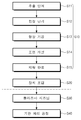
도 4는 본 발명의 일 실시 예에 따른 장치 제조 방법을 설명하기 위한 순서도이다. 도 2 및 도 4를 참고하면, 본 발명의 장치 제조 방법은 쿼츠 부재 제조 단계(S10) 및 장치 조립 단계(S20)를 포함한다.4 is a flowchart illustrating a method of manufacturing a device according to an embodiment of the present invention. Referring to Figs. 2 and 4, the apparatus manufacturing method of the present invention includes a quartz member manufacturing step S10 and an apparatus assembling step S20.
쿼츠 부재 제조 단계(S10)는 장치 조립 단계(S20) 이전에 수행된다. 쿼츠 부재 제조 단계(S10)에서는 쿼츠 부재가 제조된다. 쿼츠 부재 제조 단계(S10)는 추출 단계(S11), 합성 단계(S12), 형상 가공 단계(S13), 표면 개질 단계(S14) 및 제작 완료 단계(S15)를 포함한다. 형상 가공 단계(S13), 표면 개질 단계(S14) 및 제작 완료 단계(S15)는 서로 순차적으로 수행된다.The quartz member manufacturing step S10 is performed before the device assembling step S20. In the quartz member manufacturing step S10, a quartz member is manufactured. The quartz member manufacturing step S10 includes an extraction step S11, a synthesis step S12, a shape processing step S13, a surface modification step S14, and a production completion step S15. The shape processing step S13, the surface modification step S14, and the production completion step S15 are performed sequentially with each other.
추출 단계(S11)에서는 쿼츠 부재를 제조하기 위한 화학 합성의 재료로 사용되는 제 1 재료 및 제 1 재료와 상이한 제 2 재료를 천연 광물로부터 추출한다. 제 1 재료는 규소(Si) 원소를 포함하고, 제 2 재료는 산소(O) 원소를 포함한다. 일 실시 예에 따르면, 제 1 재료는 규소(Si) 원소만으로 구성되고, 제 2 재료는 산소(O) 원소만으로 구성된다. 따라서, 천연 광물은 쿼츠를 포함하는 광물로 제공된다. In the extraction step S11, a first material used as a material of chemical synthesis for producing the quartz member and a second material different from the first material are extracted from natural minerals. The first material comprises a silicon (Si) element and the second material comprises an oxygen (O) element. According to one embodiment, the first material consists only of silicon (Si) elements and the second material consists only of oxygen (O) elements. Thus, natural minerals are provided as minerals containing quartz.
합성 단계(S12)에서는 쿼츠 부재를 제조하기 위한 화학 합성이 수행되는 합성 챔버 내에서 제 1 재료 및 제 2 재료를 화학적으로 합성하여 쿼츠 부재로 가공하기 위한 쿼츠 재료를 합성한다. 합성 단계(S12)에서는 제 1 재료 및 제 2 재료를 합성 시, 합성 챔버 내에 질소(N) 원소를 포함하는 제 3 재료를 공급한다. 이 경우, 합성 챔버 내의 질소 원자의 수는 합성 챔버 내의 규소 원자 및 산소 원자의 수보다 작게 제공된다. 따라서, 합성 단계(S12)를 통해 쿼츠 분자들 사이에 질소(N) 성분이 혼합된 쿼츠 재료가 형성된다.In the synthesis step S12, the quartz material for synthesizing the first material and the second material chemically in the synthesis chamber in which the chemical synthesis for producing the quartz member is performed to form a quartz member is synthesized. In the synthesis step S12, when the first material and the second material are synthesized, a third material containing nitrogen (N) element is supplied into the synthesis chamber. In this case, the number of nitrogen atoms in the synthesis chamber is provided smaller than the number of silicon atoms and oxygen atoms in the synthesis chamber. Thus, through the synthesis step S12, a quartz material in which a nitrogen (N) component is mixed between quartz molecules is formed.
형상 가공 단계(S13)에서는 합성 단계(S12)에서 생성된 쿼츠 재질을 이용하여 쿼츠 부재를 요구되는 형상으로 가공한다. 예를 들면, 쿼츠 부재가 유전판(700)인 경우, 쿼츠 부재는 유전판(700)의 형상으로 가공되고, 쿼츠 부재가 라이너(900)인 경우, 쿼츠 부재는 라이너(900)의 형상으로 가공된다.In the shaping step S13, the quartz member is processed into a desired shape using the quartz material produced in the synthesis step S12. For example, when the quartz member is the
표면 개질 단계(S14)에서는 쿼츠 부재의 표면을 개질시키는 공정이 수행된다. 표면 개질 단계(S14)에서는 표면 조도 조정 단계 등 쿼츠 부재의 표면을 기판 처리 공정을 수행하기에 적당한 상태로 개질시키는 공정이 수행된다.In the surface modification step (S14), a step of modifying the surface of the quartz member is performed. In the surface modification step S14, a step of modifying the surface of the quartz member such as the surface roughness adjustment step to a state suitable for performing the substrate processing process is performed.
표면 조도 조정 단계에서는 쿼츠 부재의 표면의 조도를 조정한다. 일반적으로 표면 조도 조정 단계(S12b)에서는 쿼츠 부재에 열처리를 함으로써, 쿼츠 부재의 표면 조도를 조정한다. 이 경우, 열처리는 RTP법, 퍼니스 가압법 또는 직접 화염법 등의 방식으로 수행될 수 있다. In the surface roughness adjustment step, the roughness of the surface of the quartz member is adjusted. Generally, in the surface roughness adjusting step (S12b), the surface roughness of the quartz member is adjusted by subjecting the quartz member to heat treatment. In this case, the heat treatment may be performed by a method such as RTP method, furnace pressurization method, or direct flame method.
쿼츠 부재의 제작이 완료(S15)된 후, 장치 조립 단계(S20)에서는 쿼츠 부재 제조 단계(S10)를 통해 제조가 완료된 쿼츠 부재가 장치에 조립된다. 장치 조립 단계(S20)는 기판 처리 장치를 제조하는 장치 제조 방법에 포함되는 단계일 수 있다. 이와 달리, 장치 조립 단계(S20)는 손상되어 교체가 예정된 쿼츠 부재를 교체하기 위한 단계일 수 있다.After the production of the quartz member is completed (S15), in the device assembling step (S20), the quartz member that has been manufactured through the quartz member manufacturing step (S10) is assembled to the apparatus. The apparatus assembling step S20 may be a step included in the apparatus manufacturing method of manufacturing the substrate processing apparatus. Alternatively, the apparatus assembling step S20 may be a step for replacing the quartz member which is damaged and is intended to be replaced.
장치의 조립이 완료된 이 후, 기판 처리 장치(10)의 내부를 기판에 대한 처리 공정을 수행하기 위해 적당한 상태로 준비시키기 위한 플라스마 시즈닝 단계(S30)가 수행된다. 이 경우, 플라스마 시즈닝 단계(S30)에서는 쿼츠 부재가 기판 처리 공정 중 발생되는 플라스마에 대한 내구성을 증가시키기 위해 쿼츠 부재의 표면을 질화시키기 위한 공정이 수행된다. 이 경우, 쿼츠 부재의 표면을 질화시키는 공정은 기판 지지 유닛(200)을 보호하기 위해 기판 지지 유닛(200) 상면에 더미 기판을 놓아둔 상태로 수행된다.After the assembly of the apparatus is completed, a plasma seasoning step (S30) is performed to prepare the interior of the
시즈닝 단계(S30) 이 후, 기판 처리 장치(10) 내에서 기판에 대한 공정이 수행되는 기판 처리 공정(S40)이 수행된다.After the seasoning step S30, a substrate processing step S40 is performed in which the substrate processing is performed in the
상술한 바와 같이, 쿼츠 재질을 합성하는 합성 단계(S12)에서 규소 원소 및 산소 원소의 합성 시, 질소 원소를 공급함으로써, 합성된 쿼츠 재질을 이용하여 제조된 쿼츠 부재는 쿼츠 분자(SiO2)들 사이에 질소 원소가 혼합될 수 있다. 따라서, 질소 성분이 혼합된 쿼츠 부재는 그 자체로서 플라스마에 대한 내구성이 증가될 수 있고, 또한, 쿼츠 부재 자체에 질소 원소를 포함하고 있으므로, 쿼츠 부재의 표면 질화 공정을 수행 시, 쿼츠 부재의 질화 효율을 높일 수 있다. 그러므로, 쿼츠 부재의 질화 공정의 시간 및 횟수를 감소시킬 수 있고, 이로 인해, 쿼츠 부재의 질화 공정에서 사용되는 더미 기판의 수를 감소시킬 수 있다.As it described above, by supplying the nitrogen element in the synthesis of silicon element and oxygen element in the synthesis step of synthesizing the quartz material (S12), the prepared using the synthetic quartz material quartz member is quartz molecule (SiO 2) The nitrogen element may be mixed. Therefore, the quartz member in which the nitrogen component is mixed can increase the durability of the quartz member itself, and furthermore, the nitrogen element is contained in the quartz member itself. Therefore, when performing the surface nitriding process of the quartz member, The efficiency can be increased. Therefore, the time and frequency of the nitriding process of the quartz member can be reduced, thereby reducing the number of dummy substrates used in the nitriding process of the quartz member.
W: 기판 10; 기판 처리 장치
100: 공정 챔버 200: 기판 지지 유닛
300: 가스 공급 유닛 400: 마이크로파 인가 유닛
500: 안테나 판 600: 지파판
700: 유전판 900: 라이너
S10: 쿼츠 부재 제조 단계 S12: 합성 단계
S20: 장치 조립 단계W:
100: process chamber 200: substrate support unit
300: gas supply unit 400: microwave application unit
500: Antenna plate 600:
700: Dielectric plate 900: Liner
S10: Quartz member manufacturing step S12: Synthesis step
S20: Device assembly phase
Claims (16)
상기 플라스마에 노출되는 부품을 제조 시, 합성 챔버 내에서 제 1 재료 및 상기 제 1 재료와 상이한 제 2 재료를 화학적으로 합성하는 합성 단계와;
상기 합성 단계에서 생성된 쿼츠 재질을 요구되는 쿼츠 부재의 형상으로 가공하는 형상 가공 단계와;
가공된 상기 쿼츠 부재를 이용하여 상기 기판 처리 장치를 조립하는 단계와; 그리고
기판에 대한 처리 공정을 수행하기 전에 조립된 상기 기판 처리 장치에서 상기 쿼츠 부재의 표면을 질화시키는 공정을 수행하는 단계를 포함하되,
상기 합성 단계에서는 상기 합성 시 상기 합성 챔버 내에 질소 원소를 포함하는 제 3 재료를 공급하는 기판 처리 장치의 제조 방법.A method of manufacturing a substrate processing apparatus for processing a substrate using a plasma,
A synthesis step of chemically synthesizing a first material and a second material different from the first material in a synthesis chamber when manufacturing the parts exposed to the plasma;
A shape processing step of processing the quartz material produced in the synthesis step into a desired quartz member shape;
Assembling the substrate processing apparatus using the processed quartz member; And
And performing a process of nitriding the surface of the quartz member in the assembled substrate processing apparatus before performing a treatment process on the substrate,
Wherein the synthesis step supplies a third material containing a nitrogen element into the synthesis chamber during the synthesis.
상기 부품은 쿼츠를 포함하는 재질로 제공되고,
상기 제 1 재료는 규소 원소를 포함하고,
상기 제 2 재료는 산소 원소를 포함하는 장치 제조 방법.8. The method of claim 7,
Said part being provided in a material comprising quartz,
Wherein the first material comprises a silicon element,
Wherein the second material comprises an oxygen element.
상기 합성 단계 이전에 상기 제 1 재료 및 상기 제 2 재료를 쿼츠(Quartz)를 포함하는 천연 광물로부터 추출하는 추출 단계를 더 포함하는 장치 제조 방법.9. The method of claim 8,
Further comprising an extraction step of extracting the first material and the second material from natural minerals including Quartz prior to the synthesis step.
상기 합성 단계에서, 상기 합성 챔버 내의 질소 원자의 수는 상기 합성 챔버 내의 규소 원자 및 산소 원자의 수보다 작게 제공되는 장치 제조 방법.9. The method of claim 8,
Wherein in the synthesis step, the number of nitrogen atoms in the synthesis chamber is less than the number of silicon atoms and oxygen atoms in the synthesis chamber.
상기 제 1 재료는 규소 원소만으로 구성되고,
상기 제 2 재료는 산소 원소만으로 구성된 장치 제조 방법.11. The method of claim 10,
Wherein the first material is composed only of a silicon element,
Wherein the second material is composed only of oxygen elements.
상기 기판 처리 장치는 마이크로파를 안테나에 인가하여 상기 기판 처리 장치 내로 공급된 가스로부터 플라스마를 발생시키는 장치인 장치 제조 방법.12. The method according to any one of claims 7 to 11,
Wherein the substrate processing apparatus is a device that applies a microwave to an antenna to generate a plasma from a gas supplied into the substrate processing apparatus.
상기 부품은 상기 플라스마에 의해 기판이 처리되는 처리 공간의 상면에 제공된 유전판 또는 상기 처리 공간의 측면에 제공된 라이너인 장치 제조 방법.13. The method of claim 12,
Wherein the component is a dielectric plate provided on an upper surface of a processing space in which the substrate is processed by the plasma or a liner provided on a side surface of the processing space.
Priority Applications (1)
| Application Number | Priority Date | Filing Date | Title |
|---|---|---|---|
| KR1020150187208A KR101853362B1 (en) | 2015-12-28 | 2015-12-28 | Manufacturing method of substrate treating apparatus |
Applications Claiming Priority (1)
| Application Number | Priority Date | Filing Date | Title |
|---|---|---|---|
| KR1020150187208A KR101853362B1 (en) | 2015-12-28 | 2015-12-28 | Manufacturing method of substrate treating apparatus |
Publications (2)
| Publication Number | Publication Date |
|---|---|
| KR20170077378A KR20170077378A (en) | 2017-07-06 |
| KR101853362B1 true KR101853362B1 (en) | 2018-04-30 |
Family
ID=59354104
Family Applications (1)
| Application Number | Title | Priority Date | Filing Date |
|---|---|---|---|
| KR1020150187208A Active KR101853362B1 (en) | 2015-12-28 | 2015-12-28 | Manufacturing method of substrate treating apparatus |
Country Status (1)
| Country | Link |
|---|---|
| KR (1) | KR101853362B1 (en) |
Families Citing this family (1)
| Publication number | Priority date | Publication date | Assignee | Title |
|---|---|---|---|---|
| WO2019053925A1 (en) * | 2017-09-12 | 2019-03-21 | 株式会社Kokusai Electric | Semiconductor device manufacturing method, substrate treatment device, and program |
Citations (1)
| Publication number | Priority date | Publication date | Assignee | Title |
|---|---|---|---|---|
| US20090277782A1 (en) * | 2007-09-18 | 2009-11-12 | College Of William And Mary | Silicon Oxynitride Coating Compositions |
-
2015
- 2015-12-28 KR KR1020150187208A patent/KR101853362B1/en active Active
Patent Citations (1)
| Publication number | Priority date | Publication date | Assignee | Title |
|---|---|---|---|---|
| US20090277782A1 (en) * | 2007-09-18 | 2009-11-12 | College Of William And Mary | Silicon Oxynitride Coating Compositions |
Also Published As
| Publication number | Publication date |
|---|---|
| KR20170077378A (en) | 2017-07-06 |
Similar Documents
| Publication | Publication Date | Title |
|---|---|---|
| KR20160002543A (en) | Substrate treating apparatus | |
| EP2276328A1 (en) | Microwave plasma processing device | |
| US20150118416A1 (en) | Substrate treating apparatus and method | |
| KR101757816B1 (en) | Method and apparatus for treating substrate | |
| KR101853362B1 (en) | Manufacturing method of substrate treating apparatus | |
| KR102175082B1 (en) | Substrate treating apparatus | |
| JP2011150943A (en) | Plasma processing apparatus, and substrate processing method employing the same | |
| KR101966807B1 (en) | Apparatus for treating substrate | |
| KR101528457B1 (en) | Apparatus and method for treating substrate | |
| KR102175080B1 (en) | Apparatus and method for treating substrate | |
| KR102493574B1 (en) | Apparatus for treating substrate | |
| CN110010438B (en) | Plasma processing apparatus and method for manufacturing plasma processing apparatus | |
| KR101842116B1 (en) | Quartz member manufacturing method, apparatus manufacturing method and substrate treating apparatus | |
| KR20170098996A (en) | Apparatus and method for treating substrate | |
| KR101736839B1 (en) | Apparatus and method for treating substrate | |
| KR101966810B1 (en) | Substrate treating apparatus and substrate treating method | |
| KR102108318B1 (en) | Substrate treating apparatus | |
| KR20100012418A (en) | Plasma reactor apparatus having magnetism control constitution | |
| KR102344527B1 (en) | Apparatus and method for treating substrate | |
| KR101736842B1 (en) | Dielectric plate and substrate treating apparatus including the same | |
| KR101681182B1 (en) | Substrate treating apparatus | |
| KR102278075B1 (en) | Dielectric plate and substrate processing apparatus using the same | |
| KR20160002544A (en) | Apparatus for treating substrate | |
| KR101736840B1 (en) | Antenna and substrate treating apparatus including the same | |
| KR101934983B1 (en) | Apparatus for treating substrate |
Legal Events
| Date | Code | Title | Description |
|---|---|---|---|
| A201 | Request for examination | ||
| PA0109 | Patent application |
St.27 status event code: A-0-1-A10-A12-nap-PA0109 |
|
| PA0201 | Request for examination |
St.27 status event code: A-1-2-D10-D11-exm-PA0201 |
|
| D13-X000 | Search requested |
St.27 status event code: A-1-2-D10-D13-srh-X000 |
|
| D14-X000 | Search report completed |
St.27 status event code: A-1-2-D10-D14-srh-X000 |
|
| E902 | Notification of reason for refusal | ||
| PE0902 | Notice of grounds for rejection |
St.27 status event code: A-1-2-D10-D21-exm-PE0902 |
|
| P11-X000 | Amendment of application requested |
St.27 status event code: A-2-2-P10-P11-nap-X000 |
|
| P13-X000 | Application amended |
St.27 status event code: A-2-2-P10-P13-nap-X000 |
|
| PG1501 | Laying open of application |
St.27 status event code: A-1-1-Q10-Q12-nap-PG1501 |
|
| E90F | Notification of reason for final refusal | ||
| PE0902 | Notice of grounds for rejection |
St.27 status event code: A-1-2-D10-D21-exm-PE0902 |
|
| T11-X000 | Administrative time limit extension requested |
St.27 status event code: U-3-3-T10-T11-oth-X000 |
|
| T11-X000 | Administrative time limit extension requested |
St.27 status event code: U-3-3-T10-T11-oth-X000 |
|
| E13-X000 | Pre-grant limitation requested |
St.27 status event code: A-2-3-E10-E13-lim-X000 |
|
| P11-X000 | Amendment of application requested |
St.27 status event code: A-2-2-P10-P11-nap-X000 |
|
| P13-X000 | Application amended |
St.27 status event code: A-2-2-P10-P13-nap-X000 |
|
| E701 | Decision to grant or registration of patent right | ||
| PE0701 | Decision of registration |
St.27 status event code: A-1-2-D10-D22-exm-PE0701 |
|
| GRNT | Written decision to grant | ||
| PR0701 | Registration of establishment |
St.27 status event code: A-2-4-F10-F11-exm-PR0701 |
|
| PR1002 | Payment of registration fee |
St.27 status event code: A-2-2-U10-U11-oth-PR1002 Fee payment year number: 1 |
|
| PG1601 | Publication of registration |
St.27 status event code: A-4-4-Q10-Q13-nap-PG1601 |
|
| P22-X000 | Classification modified |
St.27 status event code: A-4-4-P10-P22-nap-X000 |
|
| PR1001 | Payment of annual fee |
St.27 status event code: A-4-4-U10-U11-oth-PR1001 Fee payment year number: 4 |
|
| PR1001 | Payment of annual fee |
St.27 status event code: A-4-4-U10-U11-oth-PR1001 Fee payment year number: 5 |
|
| PN2301 | Change of applicant |
St.27 status event code: A-5-5-R10-R13-asn-PN2301 St.27 status event code: A-5-5-R10-R11-asn-PN2301 |
|
| R18-X000 | Changes to party contact information recorded |
St.27 status event code: A-5-5-R10-R18-oth-X000 |
|
| PR1001 | Payment of annual fee |
St.27 status event code: A-4-4-U10-U11-oth-PR1001 Fee payment year number: 6 |
|
| PR1001 | Payment of annual fee |
St.27 status event code: A-4-4-U10-U11-oth-PR1001 Fee payment year number: 7 |
|
| PN2301 | Change of applicant |
St.27 status event code: A-5-5-R10-R13-asn-PN2301 St.27 status event code: A-5-5-R10-R11-asn-PN2301 |
|
| PR1001 | Payment of annual fee |
St.27 status event code: A-4-4-U10-U11-oth-PR1001 Fee payment year number: 8 |
|
| P22-X000 | Classification modified |
St.27 status event code: A-4-4-P10-P22-nap-X000 |