KR101850510B1 - precursor composition for oxide semiconductor and manufacturing method of thin film transistor array panel using the same - Google Patents
precursor composition for oxide semiconductor and manufacturing method of thin film transistor array panel using the same Download PDFInfo
- Publication number
- KR101850510B1 KR101850510B1 KR1020110025304A KR20110025304A KR101850510B1 KR 101850510 B1 KR101850510 B1 KR 101850510B1 KR 1020110025304 A KR1020110025304 A KR 1020110025304A KR 20110025304 A KR20110025304 A KR 20110025304A KR 101850510 B1 KR101850510 B1 KR 101850510B1
- Authority
- KR
- South Korea
- Prior art keywords
- delete delete
- metal
- oxide semiconductor
- thin film
- compound solution
- Prior art date
- Legal status (The legal status is an assumption and is not a legal conclusion. Google has not performed a legal analysis and makes no representation as to the accuracy of the status listed.)
- Active
Links
Images


Classifications
-
- H10P14/265—
-
- C—CHEMISTRY; METALLURGY
- C23—COATING METALLIC MATERIAL; COATING MATERIAL WITH METALLIC MATERIAL; CHEMICAL SURFACE TREATMENT; DIFFUSION TREATMENT OF METALLIC MATERIAL; COATING BY VACUUM EVAPORATION, BY SPUTTERING, BY ION IMPLANTATION OR BY CHEMICAL VAPOUR DEPOSITION, IN GENERAL; INHIBITING CORROSION OF METALLIC MATERIAL OR INCRUSTATION IN GENERAL
- C23C—COATING METALLIC MATERIAL; COATING MATERIAL WITH METALLIC MATERIAL; SURFACE TREATMENT OF METALLIC MATERIAL BY DIFFUSION INTO THE SURFACE, BY CHEMICAL CONVERSION OR SUBSTITUTION; COATING BY VACUUM EVAPORATION, BY SPUTTERING, BY ION IMPLANTATION OR BY CHEMICAL VAPOUR DEPOSITION, IN GENERAL
- C23C16/00—Chemical coating by decomposition of gaseous compounds, without leaving reaction products of surface material in the coating, i.e. chemical vapour deposition [CVD] processes
- C23C16/22—Chemical coating by decomposition of gaseous compounds, without leaving reaction products of surface material in the coating, i.e. chemical vapour deposition [CVD] processes characterised by the deposition of inorganic material, other than metallic material
- C23C16/30—Deposition of compounds, mixtures or solid solutions, e.g. borides, carbides, nitrides
- C23C16/40—Oxides
-
- H—ELECTRICITY
- H10—SEMICONDUCTOR DEVICES; ELECTRIC SOLID-STATE DEVICES NOT OTHERWISE PROVIDED FOR
- H10D—INORGANIC ELECTRIC SEMICONDUCTOR DEVICES
- H10D86/00—Integrated devices formed in or on insulating or conducting substrates, e.g. formed in silicon-on-insulator [SOI] substrates or on stainless steel or glass substrates
- H10D86/40—Integrated devices formed in or on insulating or conducting substrates, e.g. formed in silicon-on-insulator [SOI] substrates or on stainless steel or glass substrates characterised by multiple TFTs
- H10D86/60—Integrated devices formed in or on insulating or conducting substrates, e.g. formed in silicon-on-insulator [SOI] substrates or on stainless steel or glass substrates characterised by multiple TFTs wherein the TFTs are in active matrices
-
- H10P14/3426—
-
- H10P14/3434—
Landscapes
- Chemical & Material Sciences (AREA)
- Inorganic Chemistry (AREA)
- General Chemical & Material Sciences (AREA)
- Chemical Kinetics & Catalysis (AREA)
- Engineering & Computer Science (AREA)
- Materials Engineering (AREA)
- Mechanical Engineering (AREA)
- Metallurgy (AREA)
- Organic Chemistry (AREA)
- Thin Film Transistor (AREA)
Abstract
산화물 반도체의 전구체 조성물을 제공한다. 본 발명의 한 실시예에 따른 산화물 반도체의 전구체 조성물은 금속 이온과 유기 리간드에 의해 형성된 금속 착화합물을 포함하고, 하기 화학식 (1)로 표시된다.
MAn 화학식 (1)
여기서, M은 금속 이온이며 A는 알파 치환된 카르복실레이트(α-substituted carboxylate)를 포함하며, n은 자연수이다.A precursor composition of an oxide semiconductor is provided. The precursor composition of an oxide semiconductor according to an embodiment of the present invention includes a metal complex formed by a metal ion and an organic ligand, and is represented by the following chemical formula (1).
MAn Formula (1)
Where M is a metal ion, A comprises an alpha-substituted carboxylate, and n is a natural number.
Description
본 발명은 산화물 반도체의 전구체 조성물 및 이를 이용한 박막 트랜지스터 표시판의 제조 방법에 관한 것이다.
The present invention relates to a precursor composition of an oxide semiconductor and a method of manufacturing a thin film transistor panel using the precursor composition.
액정 표시 장치는 현재 가장 널리 사용되고 있는 평판 표시 장치 중 하나로서, 전극이 형성되어 있는 두 장의 기판과 그 사이에 삽입되어 있는 액정층으로 이루어지며, 전극에 전압을 인가하여 액정층의 액정 분자들을 재배열시킴으로써 투과되는 빛의 양을 조절하여 영상을 표시하는 장치이다.2. Description of the Related Art [0002] A liquid crystal display device is one of the most widely used flat panel display devices, and is composed of two substrates on which electrodes are formed and a liquid crystal layer sandwiched therebetween. A voltage is applied to the electrodes to form liquid crystal molecules And displays the image by adjusting the amount of light transmitted through the array.
일반적으로, 액정 표시 장치는 각 화소를 스위칭하기 위한 박막 트랜지스터를 포함한다. 박막 트랜지스터는 스위칭 신호를 인가 받는 게이트 전극과, 데이터 전압이 인가되는 소스 전극과, 데이터 전극을 출력하는 드레인 전극을 삼단자로 하여 스위칭 소자를 이룬다. 또한 이러한 박막 트랜지스터는 게이트 전극, 소스 전극 및 드레인 전극과 중첩되어 있는 액티브층을 채널층으로 포함하며, 액티브층은 반도체 재료로서 비정질 실리콘이 주로 사용되고 있다.Generally, a liquid crystal display device includes a thin film transistor for switching each pixel. The thin film transistor forms a switching element by using a three-terminal character as a gate electrode to which a switching signal is applied, a source electrode to which a data voltage is applied, and a drain electrode to output a data electrode. Further, such a thin film transistor includes an active layer overlapping with a gate electrode, a source electrode and a drain electrode as a channel layer, and the active layer is mainly made of amorphous silicon as a semiconductor material.
그러나, 디스플레이의 대형화가 이루어짐에 따라 초고속 구동이 가능한 박막 트랜지스터의 개발이 절실해지고 있다. 특히 액티브층으로 현재 주로 사용되고 있는 비정질 실리콘은 전자 이동도가 낮고 화학 기상 증착법(Chemical vapor deposition; CVD), 스퍼터링 방법 등을 적용하기 위한 고가의 진공 공정 기반의 증착 장비들을 필요로 한다.However, as the size of the display is increased, the development of a thin film transistor capable of high-speed driving is urgently required. In particular, amorphous silicon, which is currently used mainly as an active layer, has a low electron mobility and requires expensive vacuum process-based deposition equipment for applying chemical vapor deposition (CVD), sputtering, and the like.
따라서, 전자 이동도가 높고 코팅 공정 또는 초저가 프린팅 공정을 통하여 진행하기 위해 용액 공정이 가능한 산화물 반도체 재료의 개발이 요구되고 있다.Therefore, there is a demand for the development of an oxide semiconductor material capable of performing a solution process so as to have high electron mobility and to proceed through a coating process or an ultra low-cost printing process.
그러나, 산화물 반도체를 용액 공정으로 형성하기 위해서는 400도 이상의 고온에서 열처리를 필요로 하여 에너지 소모가 크다.However, in order to form an oxide semiconductor by a solution process, heat treatment is required at a high temperature of 400 DEG C or more, and energy consumption is large.
따라서, 본 발명이 해결하고자 하는 과제는 저온 공정으로 박막 트랜지스터 특성을 가질 수 있는 산화물 반도체의 전구체 조성물 및 이를 이용한 박막 트랜지스터 표시판의 제조 방법을 제공하는데 있다.
Accordingly, an object of the present invention is to provide a precursor composition of an oxide semiconductor capable of having a thin film transistor characteristic in a low-temperature process, and a method of manufacturing a thin film transistor panel using the precursor composition.
본 발명의 한 실시예에 따른 산화물 반도체의 전구체 조성물은 금속 이온과 유기 리간드에 의해 형성된 금속 착화합물을 포함하고, 하기 화학식 (1)로 표시된다.The precursor composition of an oxide semiconductor according to an embodiment of the present invention includes a metal complex formed by a metal ion and an organic ligand, and is represented by the following chemical formula (1).
MAn 화학식 (1)MAn Formula (1)
여기서, M은 금속 이온이며 A는 알파 치환된 카르복실레이트(α-substituted carboxylate)를 포함하며, n은 자연수이다.Where M is a metal ion, A comprises an alpha-substituted carboxylate, and n is a natural number.
상기 화학식 (1)에서 A는 알파 치환된 아미노산(α-substituted amino acid), 알파 치환된 히드록시산(α-substituted hydroxyl acid), 알파 치환된 케토산(α-substituted keto acid), 및 알파 치환된 티오산(α-substituted thio acid) 중 적어도 하나를 포함할 수 있다.In the above formula (1), A is an alpha-substituted amino acid, an alpha-substituted hydroxyl acid, an alpha-substituted keto acid, Alpha-substituted thio acid. ≪ / RTI >
상기 화학식 (1)은 하기 화학식 (2)로 표시되는 화합물을 포함할 수 있다.The formula (1) may include a compound represented by the following formula (2).

여기서, M은 금속 이온이고, X는 NH2, OH, O, SH 중 적어도 하나이며, R은 수소(H) 또는 알킬 그룹(alkyl group)이고, n은 1 내지 3일 수 있다.Wherein M is a metal ion and X is at least one of NH 2 , OH, O and SH, R is hydrogen (H) or an alkyl group, and n is 1 to 3.
상기 금속 이온은 Zinc(Zn), Tin(Sn), Indium(In), Galium(Ga), lithium(Li), sodium(Na), potassium(K), rubidium(Rb), cesium(Cs), beryllium(Be), aluminum(Al), barium(Ba), zirconium(Zr), hafnium(Hf), vanadium(V), yttrium(Y), niobium(Nb), tantalum(Ta), chromium(Cr), molybdenum(Mo), tungsten(W), manganese(Mn), technetium(Tc), rhenium(Re), iron(Fe), ruthenium(Ru), osmium(Os), cobalt(Co), rhodium(Rh), iridium(Ir), nickel(Ni), palladium(Pd), platinum(Pt), gold(Au), mercury(Hg), boron(B), thallium(Tl), silicon(Si), phosphorus(P), arsenic(As), lanthanum(La), cerium(Ce), gadolinium(Gd), Neodymiun(Nd), Tellurium(Te), Scandium(Sc), Polonium(Po), Praseodymiun(Pr), Terbium(Tb), Dysprosium(Dy), Holmium(Ho), Europium(Eu), Erbium(Er), 및 Ytterbium(Yb) 중에서 적어도 하나를 포함할 수 있다.The metal ion may be selected from the group consisting of zinc (Zn), tin (Sn), indium (In), gallium (Ga), lithium (Li), sodium (Na), potassium (K), rubidium (Ba), zirconium (Zr), hafnium (Hf), vanadium (V), yttrium (Y), niobium (Nb), tantalum (Ta), chromium (Cr), molybdenum (Mo), tungsten (W), manganese (Mn), technetium (Tc), rhenium (Re), iron (Fe), ruthenium (Ru), osmium (Ir), nickel (Ni), palladium (Pd), platinum (Pt), gold (Au), mercury (Hg), boron (B), thallium (As), lanthanum (La), cerium (Ce), gadolinium (Gd), neodymium (Nd), tellurium (Te), Scandium (Sc), Polonium (Po), Praseodymium (Dy), Holmium (Ho), Europium (Eu), Erbium (Er), and Ytterbium (Yb).
상기 금속 이온과 상기 유기 리간드의 몰 비율은 1:0.2 내지 1:10일 수 있다.The molar ratio of the metal ion to the organic ligand may be from 1: 0.2 to 1:10.
상기 알파 치환된 아미노산(α-substituted amino acid)은 알라닌(alanine), 세린(serine), 글리신(glycine), 시스테인(cysteine), 프롤린(proline), 및 사르코신(sarcosine) 중 적어도 하나를 포함할 수 있다.The alpha-substituted amino acid comprises at least one of alanine, serine, glycine, cysteine, proline, and sarcosine. .
상기 알파 치환된 히드록시산(α-substituted hydroxyl acid)은 2-히드록시 아세트산(2-hydroxy acetic acid) 또는 젖산(lactic acid)을 포함할 수 있다.The alpha-substituted hydroxyl acid may include 2-hydroxy acetic acid or lactic acid.
상기 알파 치환된 케토산(α-substituted keto acid)은 피루브산(pyruvic acid) 또는 글리옥실산(glyoxylic acid)을 포함할 수 있다.The alpha-substituted keto acid may include pyruvic acid or glyoxylic acid.
상기 알파 치환된 티오산(α-substituted thio acid)은 티오락트산(thiolactic acid) 또는 티오글리콜산(thioglycolic acid)을 포함할 수 있다.The alpha-substituted thio acid may include thiolactic acid or thioglycolic acid.
본 발명의 다른 실시예에 따른 박막 트랜지스터 표시판의 제조 방법은 금속 이온과 유기 리간드에 의해 형성된 금속 착화합물 및 용매를 포함하는 금속 화합물 용액을 준비하는 단계; 상기 금속 화합물 용액을 기판 상에 코팅하는 단계; 및 상기 금속 화합물 용액을 열처리하는 단계를 포함하고, 상기 금속 착화합물은 하기 화학식 (1)로 표시된다.According to another embodiment of the present invention, there is provided a method of manufacturing a thin film transistor panel, comprising: preparing a metal compound solution including a metal complex formed by metal ions and an organic ligand and a solvent; Coating the metal compound solution on a substrate; And heat treating the metal compound solution, wherein the metal complex compound is represented by the following chemical formula (1).
MAn 화학식 (1)MAn Formula (1)
여기서, M은 금속 이온이며 A는 알파 치환된 카르복실레이트(α-substituted carboxylate)를 포함하며, n은 자연수이다.Where M is a metal ion, A comprises an alpha-substituted carboxylate, and n is a natural number.
상기 금속 화합물 용액을 열처리하는 단계 이전에 상기 금속 화합물 용액을 전처리하는 단계를 더 포함할 수 있다.The method may further include a step of pre-treating the metal compound solution before the heat treatment of the metal compound solution.
상기 금속 화합물 용액을 전처리하는 단계는 자외선을 조사하는 단계를 포함할 수 있다.The step of pretreating the metal compound solution may include irradiating ultraviolet light.
상기 금속 화합물 용액을 열처리하는 단계는 250도 이하의 온도에서 수행할 수 있다.The step of heat-treating the metal compound solution may be performed at a temperature of 250 DEG C or less.
상기 화학식 (1)에서 A는 알파 치환된 아미노산(α-substituted amino acid), 알파 치환된 히드록시산(α-substituted hydroxyl acid), 알파 치환된 케토산(α-substituted keto acid), 및 알파 치환된 티오산(α-substituted thio acid) 중 적어도 하나를 포함할 수 있다.In the above formula (1), A is an alpha-substituted amino acid, an alpha-substituted hydroxyl acid, an alpha-substituted keto acid, Alpha-substituted thio acid. ≪ / RTI >
상기 화학식 (1)은 하기 화학식 (2)로 표시되는 화합물을 포함할 수 있다.The formula (1) may include a compound represented by the following formula (2).

여기서, M은 금속 이온이고, X는 NH2, OH, O, SH 중 적어도 하나이며, R은 수소(H) 또는 알킬 그룹(alkyl group)이고, n은 1 내지 3일 수 있다.Wherein M is a metal ion and X is at least one of NH 2 , OH, O and SH, R is hydrogen (H) or an alkyl group, and n is 1 to 3.
상기 금속 이온은 Zinc(Zn), Tin(Sn), Indium(In), Galium(Ga), lithium(Li), sodium(Na), potassium(K), rubidium(Rb), cesium(Cs), beryllium(Be), aluminum(Al), barium(Ba), zirconium(Zr), hafnium(Hf), vanadium(V), yttrium(Y), niobium(Nb), tantalum(Ta), chromium(Cr), molybdenum(Mo), tungsten(W), manganese(Mn), technetium(Tc), rhenium(Re), iron(Fe), ruthenium(Ru), osmium(Os), cobalt(Co), rhodium(Rh), iridium(Ir), nickel(Ni), palladium(Pd), platinum(Pt), gold(Au), mercury(Hg), boron(B), thallium(Tl), silicon(Si), phosphorus(P), arsenic(As), lanthanum(La), cerium(Ce), gadolinium(Gd), Neodymiun(Nd), Tellurium(Te), Scandium(Sc), Polonium(Po), Praseodymiun(Pr), Terbium(Tb), Dysprosium(Dy), Holmium(Ho), Europium(Eu), Erbium(Er), 및 Ytterbium(Yb) 중에서 적어도 하나를 포함할 수 있다.The metal ion may be selected from the group consisting of zinc (Zn), tin (Sn), indium (In), gallium (Ga), lithium (Li), sodium (Na), potassium (K), rubidium (Ba), zirconium (Zr), hafnium (Hf), vanadium (V), yttrium (Y), niobium (Nb), tantalum (Ta), chromium (Cr), molybdenum (Mo), tungsten (W), manganese (Mn), technetium (Tc), rhenium (Re), iron (Fe), ruthenium (Ru), osmium (Ir), nickel (Ni), palladium (Pd), platinum (Pt), gold (Au), mercury (Hg), boron (B), thallium (As), lanthanum (La), cerium (Ce), gadolinium (Gd), neodymium (Nd), tellurium (Te), Scandium (Sc), Polonium (Po), Praseodymium (Dy), Holmium (Ho), Europium (Eu), Erbium (Er), and Ytterbium (Yb).
상기 금속 이온과 상기 유기 리간드의 몰 비율이 1:0.2 내지 1:10이 되도록 형성할 수 있다.The molar ratio of the metal ion to the organic ligand is 1: 0.2 to 1:10.
상기 알파 치환된 아미노산(α-substituted amino acid)은 알라닌(alanine), 세린(serine), 글리신(glycine), 시스테인(cysteine), 프롤린(proline), 및 사르코신(sarcosine) 중 적어도 하나를 포함할 수 있다.The alpha-substituted amino acid comprises at least one of alanine, serine, glycine, cysteine, proline, and sarcosine. .
상기 알파 치환된 히드록시산(α-substituted hydroxyl acid)은 2-히드록시 아세트산(2-hydroxy acetic acid) 또는 젖산(lactic acid)을 포함할 수 있다.The alpha-substituted hydroxyl acid may include 2-hydroxy acetic acid or lactic acid.
상기 알파 치환된 케토산(α-substituted keto acid)은 피루브산(pyruvic acid) 또는 글리옥실산(glyoxylic acid)을 포함할 수 있다.The alpha-substituted keto acid may include pyruvic acid or glyoxylic acid.
상기 알파 치환된 티오산(α-substituted thio acid)은 티오락트산(thiolactic acid) 또는 티오글리콜산(thioglycolic acid)을 포함할 수 있다.
The alpha-substituted thio acid may include thiolactic acid or thioglycolic acid.
이와 같이 본 발명의 한 실시예에 따르면, 금속 이온과 유기 리간드에 의해 형성된 금속 착화합물을 포함하는 산화물 반도체의 전구체를 사용함으로써 250도 이하의 저온에서 공정을 수행함에 따라 에너지를 저감하고, 높은 신뢰성을 얻을 수 있다.
According to one embodiment of the present invention, by using a precursor of an oxide semiconductor including a metal complex formed by a metal ion and an organic ligand, energy is reduced by performing a process at a low temperature of 250 degrees or less, Can be obtained.
도 1은 본 발명의 한 실시예에 따른 박막 트랜지스터 표시판의 단면도이다.
도 2는 본 발명의 다른 실시예에 따른 박막 트랜지스터 표시판의 단면도이다.
도 3은 본 발명의 또 다른 실시예에 따른 박막 트랜지스터 표시판에 포함되는 산화물 반도체의 제조 방법을 나타내는 흐름도이다.
도 4는 본 발명의 또 다른 실시예에 따른 박막 트랜지스터의 전달 곡선(transfer curve)을 나타내는 그래프이다.1 is a cross-sectional view of a thin film transistor panel according to an embodiment of the present invention.
2 is a cross-sectional view of a thin film transistor panel according to another embodiment of the present invention.
3 is a flowchart illustrating a method of manufacturing an oxide semiconductor included in a thin film transistor panel according to another embodiment of the present invention.
4 is a graph showing a transfer curve of a thin film transistor according to another embodiment of the present invention.
첨부한 도면들을 참조하여 본 발명의 바람직한 실시예들을 상세히 설명하기로 한다. 그러나, 본 발명은 여기서 설명되는 실시예에 한정되지 않고 다른 형태로 구체화될 수도 있다. 오히려, 여기서 소개되는 실시예들은 개시된 내용이 철저하고 완전해질 수 있도록 그리고 당업자에게 본 발명의 사상이 충분히 전달될 수 있도록 하기 위해 제공되는 것이다. DETAILED DESCRIPTION OF THE PREFERRED EMBODIMENTS Reference will now be made in detail to the preferred embodiments of the present invention, examples of which are illustrated in the accompanying drawings. However, the present invention is not limited to the embodiments described herein but may be embodied in other forms. Rather, the embodiments disclosed herein are provided so that the disclosure can be thorough and complete, and will fully convey the scope of the invention to those skilled in the art.
도면들에 있어서, 층 및 영역들의 두께는 명확성을 기하기 위하여 과장된 것이다. 또한, 층이 다른 층 또는 기판 "상"에 있다고 언급되는 경우에 그것은 다른 층 또는 기판 상에 직접 형성될 수 있거나 또는 그들 사이에 제 3의 층이 개재될 수도 있다. 명세서 전체에 걸쳐서 동일한 참조번호로 표시된 부분들은 동일한 구성요소들을 의미한다.In the drawings, the thicknesses of layers and regions are exaggerated for clarity. Also, when a layer is referred to as being "on" another layer or substrate, it may be formed directly on another layer or substrate, or a third layer may be interposed therebetween. Like numbers refer to like elements throughout the specification.
도 1은 본 발명의 한 실시예에 따른 박막 트랜지스터 표시판의 단면도이다.1 is a cross-sectional view of a thin film transistor panel according to an embodiment of the present invention.
도 1을 참고하면, 박막 트랜지스터 표시판(100)은 절연 기판(110), 게이트 전극(120), 게이트 절연막(130), 소스 전극(144), 드레인 전극(146), 및 산화물 반도체층(150)을 포함한다. 1, the thin film
절연 기판(110) 위에 게이트 신호를 전달하는 게이트 배선의 일부인 게이트 전극(120)이 배치되어 있다. 상기 절연 기판(110)으로는 유리 기판이나 플라스틱 기판 등을 사용할 수 있다. 게이트 전극(120)은 알루미늄(Al)과 알루미늄 합금 등 알루미늄 계열의 금속, 은(Ag)과 은 합금 등 은 계열의 금속, 구리(Cu)와 구리 합금 등 구리 계열의 금속, 몰리브덴(Mo)과 몰리브덴 합금 등 몰리브덴 계열의 금속, 크롬(Cr), 티타늄(Ti), 탄탈륨(Ta) 등으로 이루어질 수 있다. A
또한, 게이트 전극(120)은 물리적 성질이 다른 두 개의 도전막(미도시)을 포함하는 다중막 구조를 가질 수 있다. 이 중 한 도전막은 신호 지연이나 전압 강하를 줄일 수 있도록 낮은 비저항(resistivity)의 금속, 예를 들면 알루미늄 계열 금속, 은 계열 금속, 구리 계열 금속 등으로 이루어진다. 이와는 달리, 다른 도전막은 다른 물질, 특히 산화 아연(ZnO), ITO(indium tin oxide) 및 IZO(indium zinc oxide)와의 접촉 특성이 우수한 물질, 이를테면 몰리브덴 계열 금속, 크롬, 티타늄, 탄탈륨 등으로 이루어진다. 이러한 조합의 좋은 예로는 크롬 하부막과 알루미늄 상부막, 알루미늄 하부막과 몰리브덴 상부막, 또는 티타늄 하부막과 구리 상부막을 들 수 있다. In addition, the
다만, 본 발명은 이에 한정되지 않으며, 게이트 전극(120)은 다양한 여러 가지 금속과 도전체로 만들어질 수 있다. However, the present invention is not limited thereto, and the
절연 기판(110) 및 게이트 전극(120)을 포함하는 게이트 배선의 위에는 게이트 절연막(130)이 형성되어 있다. 게이트 절연막(130)은 산화 규소(SiOx), 질화 규소(SiNx) 또는 산질화 규소(SiON) 등으로 형성될 수 있다. 또한 게이트 절연막(130)은 산화 규소와 질화 규소가 적층된 다층막 구조를 가질 수 있다. 이 경우 절연 기판(110)의 상부에는 질화 규소층이 형성되고 상기 질화 규소층의 상부에 산화 규소층이 형성됨으로써 산화 규소층이 후술할 산화물 반도체층과 접할 수 있다. A
산질화 규소 단일막을 사용하는 경우에도 산화물 반도체 층과 인접할수록 산질화 규소에서 산소의 조성비가 높아지도록 산소 농도에 분포를 가지게 할 수 있다. 이렇듯 산화물 반도체 층과 산화 규소 층이 접하게 되는 경우 산화물 반도체 내의 산소 결핍(oxygen deficiency) 농도를 일정하게 유지할 수 있게 되어 채널층의 열화를 방지할 수 있다. Even when a single silicon oxynitride film is used, the oxygen concentration can be distributed so that the composition ratio of oxygen in the silicon oxynitride increases so as to be closer to the oxide semiconductor layer. When the oxide semiconductor layer and the silicon oxide layer are in contact with each other, the oxygen deficiency concentration in the oxide semiconductor can be kept constant, thereby preventing deterioration of the channel layer.
게이트 절연막(130) 위에는 데이터 배선에 포함되는 소스 전극(144) 및 드레인 전극(146)이 배치되어 있다. 또한 소스 전극(144) 및 드레인 전극(146)의 상부에는 산화물 반도체층(150)이 배치되어 있다. 도시되어 있지는 않으나, 산화물 반도체층(150)의 상부에는 보호층이 배치될 수 있다. 본 실시예에서는 게이트 전극(120), 게이트 절연막(130), 소스 전극(144) 및 드레인 전극(146), 산화물 반도체층(150)이 순서대로 적층되어 있으나, 배치 순서나 위치가 다르게 형성될 수 있다. On the
소스 전극(144) 및 드레인 전극(146)은 서로 이격되어 형성되며 산화물 반도체층(150)과 적어도 일부가 중첩하게 된다. 즉, 소스 전극(144)은 산화물 반도체층(150)과 적어도 일부분이 중첩되고, 드레인 전극(146)은 산화물 박막 트랜지스터의 채널부를 중심으로 소스 전극(144)과 대향하며 산화물 반도체층(150)과 적어도 일부분이 중첩된다.The
소스 전극(144) 및 드레인 전극(146)은 산화물 반도체층(150)과 직접 접촉하여 오믹 콘택(Ohmic contact)을 형성하는 물질로 구성될 수 있는데, 산화물 반도체층(150)을 구성하는 물질보다 일함수(work function)가 작은 물질로 이루어지면 두 층간에 오믹 콘택이 이루어질 수 있다. 한편, 실시예에 따라서는 소스 전극(144) 및 드레인 전극(146)과 산화물 반도체층(150)이 중첩하는 영역에만 형성되어 있는 저항성 접촉층(미도시)을 더 포함할 수 있다. 저항성 접촉층은 오믹 콘택이 이루어지도록 도움을 주는 역할을 수행한다.The
소스 전극(144) 및 드레인 전극(146)은 게이트 전극(120)과 마찬가지로 알루미늄(Al)과 알루미늄 합금 등 알루미늄 계열의 금속, 은(Ag)과 은 합금 등 은 계열의 금속, 구리(Cu)와 구리 합금 등 구리 계열의 금속, 몰리브덴(Mo)과 몰리브덴 합금 등 몰리브덴 계열의 금속, 크롬(Cr), 티타늄(Ti), 탄탈륨(Ta) 등으로 이루어질 수 있다. 또한 산화 아연(ZnO), ITO(indium tin oxide) 및 IZO(indium zinc oxide)과 같은 투명 도전성 물질로 이루어질 수도 있다. Like the
또한, 데이터 배선은 서로 다른 두 개의 도전막(미도시)을 포함하는 다중막 구조를 가질 수 있으며, 이러한 조합의 예로는 Mo(Mo 합금)/Al(Al 합금), Ti(Ti 합금)/Al(Al 합금), Ta(Ta 합금)/Al(Al 합금), Ni(Ni 합금)/Al(Al 합금), Co(Co 합금)/Al(Al 합금), Ti(Ti 합금)/Cu(Cu 합금), Cu(Cu 합금)/Mn(Mn 합금) 등과 같은 이중막 또는 Ti(Ti 합금)/Al(Al 합금)/Ti(Ti 합금), Ta(Ta 합금)/ Al(Al 합금)/Ta(Ta 합금), Ti(Ti 합금)/Al(Al 합금)/TiN, Ta(Ta 합금)/Al(Al 합금)/TaN, Ni(Ni 합금)/Al(Al 합금)/Ni(Ni 합금), Co(Co 합금)/Al(Al 합금)/Co(Co 합금), Mo(Mo 합금)/Al(Al 합금)/Mo(Mo 합금) 등과 같은 삼중막을 들 수 있다. The data wiring may have a multilayer structure including two different conductive films (not shown). Examples of such combinations include Mo (Mo alloy) / Al (Al alloy), Ti (Ti alloy) / Al (Al alloy), Ta (Ta alloy) / Al (Al alloy), Ni (Ni alloy) / Al (Al alloy), Co (Co alloy) / Al Ti (Al alloy) / Ti (Ti alloy), Ta (Ta alloy) / Al (Al alloy) / Ta (Ta alloy) or Cu (Cu alloy) / Mn (Ni alloy) / Al (Al alloy) / Ni (Ni alloy) / Ti (Ta alloy) / Ti (Ti alloy) / Al , A Co (Co alloy) / Al (Al alloy) / Co (Co alloy), Mo (Mo alloy) / Al (Al alloy) / Mo (Mo alloy)
특히 데이터 배선으로 Cu 또는 Cu 합금을 적용할 경우에는, 데이터 배선과 화소 전극(미도시)과의 오믹 콘택 특성은 큰 문제가 없기 때문에 데이터 배선으로 Cu 또는 Cu 합금막과 산화물 반도체층(150)의 사이에 Mo, Ti 또는 Ta를 포함하는 막이 적용된 이중막이 적용될 수 있다. 다만, 본 발명은 이에 한정되지 않으며, 소스 전극(144) 및 드레인 전극(146)은 다양한 여러 가지 금속과 도전체로 만들어질 수 있다.Particularly, when Cu or a Cu alloy is applied to the data wiring, there is no great problem in the ohmic contact characteristics between the data wiring and the pixel electrode (not shown). Therefore, the Cu or Cu alloy film and the oxide semiconductor layer 150 A double film to which a film containing Mo, Ti or Ta is applied can be applied. However, the present invention is not limited thereto, and the
드레인 전극(146)은 화소 전극(도시하지 않음)과 전기적으로 연결될 수 있으며, 화소 전극에 인가된 전압에 의하여 전계가 형성되며, 그 전계에 따라서 계조 표현이 가능하도록 할 수 있다.The
소스 전극(144) 및 드레인 전극(146)의 상부에는 금속 산화물을 포함하는 산화물 반도체층(150)이 형성되어 있다. 산화물 반도체층(150)은 금속 무기염(metal inorganic salt)을 더 포함할 수 있다. 산화물 반도체층(150)은 게이트 전극(120)과도 중첩되며, 산화물 반도체층(150)과 게이트 전극(120)의 사이에는 게이트 절연막(130)과 소스 전극(144) 및 드레인 전극(146)이 배치되어 있다. An
산화물 반도체층(150)은 금속 이온과 유기 리간드에 의해 형성된 금속 착화합물을 포함하고, 하기 화학식 (1)로 표시되는 산화물 반도체의 전구체 조성물 및 용매를 포함하는 금속 화합물 용액을 코팅한 후 열처리하여 형성된다.The
MAn 화학식 (1)MAn Formula (1)
여기서, M은 금속 이온이며 A는 알파 치환된 카르복실레이트(α-substituted carboxylate)를 포함하며, n은 자연수이다.Where M is a metal ion, A comprises an alpha-substituted carboxylate, and n is a natural number.
상기 화학식 (1)에서 A는 알파 치환된 아미노산(α-substituted amino acid), 알파 치환된 히드록시산(α-substituted hydroxyl acid), 알파 치환된 케토산(α-substituted keto acid), 및 알파 치환된 티오산(α-substituted thio acid) 중 적어도 하나를 포함할 수 있다.In the above formula (1), A is an alpha-substituted amino acid, an alpha-substituted hydroxyl acid, an alpha-substituted keto acid, Alpha-substituted thio acid. ≪ / RTI >
상기 알파 치환된 아미노산(α-substituted amino acid)은 알라닌(alanine), 세린(serine), 글리신(glycine), 시스테인(cysteine), 프롤린(proline), 및 사르코신(sarcosine) 중 적어도 하나를 포함할 수 있다.The alpha-substituted amino acid comprises at least one of alanine, serine, glycine, cysteine, proline, and sarcosine. .
상기 알파 치환된 히드록시산(α-substituted hydroxyl acid)은 2-히드록시 아세트산(2-hydroxy acetic acid) 또는 젖산(lactic acid)을 포함할 수 있다.The alpha-substituted hydroxyl acid may include 2-hydroxy acetic acid or lactic acid.
상기 알파 치환된 케토산(α-substituted keto acid)은 피루브산(pyruvic acid) 또는 글리옥실산(glyoxylic acid)을 포함할 수 있다.The alpha-substituted keto acid may include pyruvic acid or glyoxylic acid.
상기 알파 치환된 티오산(α-substituted thio acid)은 티오락트산(thiolactic acid) 또는 티오글리콜산(thioglycolic acid)을 포함할 수 있다.The alpha-substituted thio acid may include thiolactic acid or thioglycolic acid.
좀 더 구체적으로 상기 화학식 (1)은 하기 화학식 (2)로 표시되는 화합물을 포함할 수 있다.More specifically, the formula (1) may include a compound represented by the following formula (2).

여기서, M은 금속 이온이고, X는 NH2, OH, O, SH 중 적어도 하나이며, R은 수소(H) 또는 알킬 그룹(alkyl group)이고, n은 1 내지 3일 수 있다.Wherein M is a metal ion and X is at least one of NH 2 , OH, O and SH, R is hydrogen (H) or an alkyl group, and n is 1 to 3.
상기 금속 이온은 Zinc(Zn), Tin(Sn), Indium(In), Galium(Ga), lithium(Li), sodium(Na), potassium(K), rubidium(Rb), cesium(Cs), beryllium(Be), aluminum(Al), barium(Ba), zirconium(Zr), hafnium(Hf), vanadium(V), yttrium(Y), niobium(Nb), tantalum(Ta), chromium(Cr), molybdenum(Mo), tungsten(W), manganese(Mn), technetium(Tc), rhenium(Re), iron(Fe), ruthenium(Ru), osmium(Os), cobalt(Co), rhodium(Rh), iridium(Ir), nickel(Ni), palladium(Pd), platinum(Pt), gold(Au), mercury(Hg), boron(B), thallium(Tl), silicon(Si), phosphorus(P), arsenic(As), lanthanum(La), cerium(Ce), gadolinium(Gd), Neodymiun(Nd), Tellurium(Te), Scandium(Sc), Polonium(Po), Praseodymiun(Pr), Terbium(Tb), Dysprosium(Dy), Holmium(Ho), Europium(Eu), Erbium(Er), 및 Ytterbium(Yb) 중에서 적어도 하나를 포함할 수 있다.The metal ion may be selected from the group consisting of zinc (Zn), tin (Sn), indium (In), gallium (Ga), lithium (Li), sodium (Na), potassium (K), rubidium (Ba), zirconium (Zr), hafnium (Hf), vanadium (V), yttrium (Y), niobium (Nb), tantalum (Ta), chromium (Cr), molybdenum (Mo), tungsten (W), manganese (Mn), technetium (Tc), rhenium (Re), iron (Fe), ruthenium (Ru), osmium (Ir), nickel (Ni), palladium (Pd), platinum (Pt), gold (Au), mercury (Hg), boron (B), thallium (As), lanthanum (La), cerium (Ce), gadolinium (Gd), neodymium (Nd), tellurium (Te), Scandium (Sc), Polonium (Po), Praseodymium (Dy), Holmium (Ho), Europium (Eu), Erbium (Er), and Ytterbium (Yb).
상기 금속 이온과 상기 유기 리간드의 몰 비율은 1:0.2 내지 1:10일 수 있다. 상기 몰 비율의 범위를 벗어나면 박막 트랜지스터의 특성이 나빠진다.The molar ratio of the metal ion to the organic ligand may be from 1: 0.2 to 1:10. If the molar ratio is out of the range, the characteristics of the thin film transistor are deteriorated.
상기 금속 화합물 용액은 안정제(stabilizer)를 더 포함할 수 있다. 상기 안정제는 다이케톤(diketone), 아미노 알코올(amino alcohol) 및 폴리아민(polyamine)으로 이루어진 군으로부터 선택된 적어도 하나를 포함한다.The metal compound solution may further include a stabilizer. The stabilizer includes at least one selected from the group consisting of diketone, amino alcohol and polyamine.
상기 용매로는 물, 에테르 및 알코올로 이루어진 군으로부터 선택된 적어도 하나를 포함한다.The solvent includes at least one selected from the group consisting of water, an ether and an alcohol.
한편, 도시되지는 않았으나 상기 산화물 반도체층(150)의 상부에는 보호막이 배치될 수 있다. 상기 보호막은 산화 규소(SiOx) 및 질화 규소(SiNx)가 적층된 다층막을 사용할 수 있으며, 산화 규소(SiOx)층이 산화물 반도체층(150)과 접하게 함으로써, 채널층의 열화를 방지할 수 있다. Although not shown, a protective layer may be disposed on the
이하에서는 도 2를 참조하여 본 발명의 다른 일 실시예에 대하여 설명한다. 도 2는 본 발명의 다른 실시예에 따른 박막 트랜지스터 표시판의 단면도이다.Hereinafter, another embodiment of the present invention will be described with reference to FIG. 2 is a cross-sectional view of a thin film transistor panel according to another embodiment of the present invention.
도 2를 참조하면, 박막 트랜지스터 기판(200)은 절연 기판(210), 게이트 전극(220), 게이트 절연막(230), 소스 전극(244), 드레인 전극(246), 및 산화물 반도체층(250)을 포함한다. 2, the thin
절연 기판(210) 위에 게이트 신호를 전달하는 게이트 배선의 일부인 게이트 전극(220)이 배치되어 있다. 절연 기판(210) 및 게이트 전극(220)의 위에는 게이트 절연막(230)이 배치되어 있다. 게이트 절연막(230)의 상부에는 게이트 전극(220)과 중첩되도록 산화물 반도체층(250)이 배치되어 있다. 산화물 반도체층(250)의 상부에는 소스 전극(244) 및 드레인 전극(246)이 배치되어 있다. 소스 전극(244) 및 드레인 전극(246)은 산화물 반도체층(250)과 적어도 일부가 중첩하고 서로 이격되어 형성된다. 즉, 산화물 반도체층(250)은 상기 게이트 절연막(230)과 상기 소스 전극(244) 및 드레인 전극(246)의 사이에 배치되어 있다. 소스 전극(244) 및 드레인 전극(246)의 상부에는 산화 규소층을 포함하는 보호막(미도시)이 배치될 수 있다. A
본 실시예의 구성 요소인 절연 기판(210), 게이트 전극(220), 게이트 절연막(230), 소스 전극(244), 드레인 전극(246), 및 산화물 반도체층(250)에 대한 자세한 설명은 앞선 실시예에서 설명한 바와 동일하므로 생략한다. A detailed description of the insulating
이상의 실시예들에서는 게이트 전극이 산화물 반도체층 아래에 배치된 바텀 게이트 구조(bottom gate structure)에 대해서 설명하였으나, 본 발명은 이에 한정되지 않으며 게이트 전극이 산화물 반도체층 위에 배치된 탑 게이트 구조(top gate structure)에서도 적용될 수 있다.Although the bottom gate structure in which the gate electrode is disposed under the oxide semiconductor layer has been described in the above embodiments, the present invention is not limited thereto, and the gate electrode may be a top gate structure disposed on the oxide semiconductor layer structure.
이하에서는, 본 발명의 박막 트랜지스터 기판의 제조 과정을 보다 상세히 설명하기로 한다.Hereinafter, a manufacturing process of the thin film transistor substrate of the present invention will be described in more detail.
도 3은 본 발명의 또 다른 실시예에 따른 박막 트랜지스터 표시판에 포함되는 산화물 반도체의 제조 방법을 나타내는 흐름도이다.3 is a flowchart illustrating a method of manufacturing an oxide semiconductor included in a thin film transistor panel according to another embodiment of the present invention.
본 실시예에 따른 박막 트랜지스터 표시판의 제조 방법은 금속 이온 및 유기 리간드에 의해 형성된 금속 착화합물 및 용매를 포함하는 금속 화합물 용액을 준비하는 단계(S1), 상기 금속 화합물 용액을 기판 위에 코팅하는 단계(S2), 상기 금속 화합물 용액을 전처리하는 단계(S3) 및 상기 금속 화합물 용액을 열처리하는 단계(S4)를 포함한다.A method of manufacturing a thin film transistor panel according to an embodiment of the present invention includes the steps of preparing a metal compound solution including a metal complex and a solvent formed by metal ions and organic ligands (S1), coating the metal compound solution on a substrate (S2 , A step (S3) of pre-treating the metal compound solution, and a step (S4) of heat-treating the metal compound solution.
금속 화합물 용액을 준비하는 단계(S1)에서는 소정의 용매에 금속 이온염 화합물을 첨가하여 교반한다. 상기 금속 이온염 화합물은 금속 이온과 유기 리간드에 의해 형성된 금속 착화합물이고, 하기 화학식 (1)로 표시되는 산화물 반도체의 전구체이다.In step (S1) of preparing a metal compound solution, a metal ion salt compound is added to a predetermined solvent and stirred. The metal ion salt compound is a metal complex formed by a metal ion and an organic ligand, and is a precursor of an oxide semiconductor represented by the following chemical formula (1).
MAn 화학식 (1)MAn Formula (1)
여기서, M은 금속 이온이며 A는 알파 치환된 카르복실레이트(α-substituted carboxylate)를 포함하며, n은 자연수이다.Where M is a metal ion, A comprises an alpha-substituted carboxylate, and n is a natural number.
상기 화학식 (1)에서 A는 알파 치환된 아미노산(α-substituted amino acid), 알파 치환된 히드록시산(α-substituted hydroxyl acid), 알파 치환된 케토산(α-substituted keto acid), 및 알파 치환된 티오산(α-substituted thio acid) 중 적어도 하나를 포함할 수 있다.In the above formula (1), A is an alpha-substituted amino acid, an alpha-substituted hydroxyl acid, an alpha-substituted keto acid, Alpha-substituted thio acid. ≪ / RTI >
상기 알파 치환된 아미노산(α-substituted amino acid)은 알라닌(alanine), 세린(serine), 글리신(glycine), 시스테인(cysteine), 프롤린(proline), 및 사르코신(sarcosine) 중 적어도 하나를 포함할 수 있다.The alpha-substituted amino acid comprises at least one of alanine, serine, glycine, cysteine, proline, and sarcosine. .
상기 알파 치환된 히드록시산(α-substituted hydroxyl acid)은 2-히드록시 아세트산(2-hydroxy acetic acid) 또는 젖산(lactic acid)을 포함할 수 있다.The alpha-substituted hydroxyl acid may include 2-hydroxy acetic acid or lactic acid.
상기 알파 치환된 케토산(α-substituted keto acid)은 피루브산(pyruvic acid) 또는 글리옥실산(glyoxylic acid)을 포함할 수 있다.The alpha-substituted keto acid may include pyruvic acid or glyoxylic acid.
상기 알파 치환된 티오산(α-substituted thio acid)은 티오락트산(thiolactic acid) 또는 티오글리콜산(thioglycolic acid)을 포함할 수 있다.The alpha-substituted thio acid may include thiolactic acid or thioglycolic acid.
좀 더 구체적으로 상기 화학식 (1)은 하기 화학식 (2)로 표시되는 화합물을 포함할 수 있다.More specifically, the formula (1) may include a compound represented by the following formula (2).

여기서, M은 금속 이온이고, X는 NH2, OH, O, SH 중 적어도 하나이며, R은 수소(H) 또는 알킬 그룹(alkyl group)이고, n은 1 내지 3일 수 있다.Wherein M is a metal ion and X is at least one of NH 2 , OH, O and SH, R is hydrogen (H) or an alkyl group, and n is 1 to 3.
상기 금속 이온은 Zinc(Zn), Tin(Sn), Indium(In), Galium(Ga), lithium(Li), sodium(Na), potassium(K), rubidium(Rb), cesium(Cs), beryllium(Be), aluminum(Al), barium(Ba), zirconium(Zr), hafnium(Hf), vanadium(V), yttrium(Y), niobium(Nb), tantalum(Ta), chromium(Cr), molybdenum(Mo), tungsten(W), manganese(Mn), technetium(Tc), rhenium(Re), iron(Fe), ruthenium(Ru), osmium(Os), cobalt(Co), rhodium(Rh), iridium(Ir), nickel(Ni), palladium(Pd), platinum(Pt), gold(Au), mercury(Hg), boron(B), thallium(Tl), silicon(Si), phosphorus(P), arsenic(As), lanthanum(La), cerium(Ce), gadolinium(Gd), Neodymiun(Nd), Tellurium(Te), Scandium(Sc), Polonium(Po), Praseodymiun(Pr), Terbium(Tb), Dysprosium(Dy), Holmium(Ho), Europium(Eu), Erbium(Er), 및 Ytterbium(Yb) 중에서 적어도 하나를 포함할 수 있다.The metal ion may be selected from the group consisting of zinc (Zn), tin (Sn), indium (In), gallium (Ga), lithium (Li), sodium (Na), potassium (K), rubidium (Ba), zirconium (Zr), hafnium (Hf), vanadium (V), yttrium (Y), niobium (Nb), tantalum (Ta), chromium (Cr), molybdenum (Mo), tungsten (W), manganese (Mn), technetium (Tc), rhenium (Re), iron (Fe), ruthenium (Ru), osmium (Ir), nickel (Ni), palladium (Pd), platinum (Pt), gold (Au), mercury (Hg), boron (B), thallium (As), lanthanum (La), cerium (Ce), gadolinium (Gd), neodymium (Nd), tellurium (Te), Scandium (Sc), Polonium (Po), Praseodymium (Dy), Holmium (Ho), Europium (Eu), Erbium (Er), and Ytterbium (Yb).
상기 금속 이온과 상기 유기 리간드의 몰 비율이 1:0.2 내지 1:10이되도록 형성할 수 있다. 상기 몰 비율의 범위를 벗어나면 박막 트랜지스터의 특성이 나빠진다.The molar ratio of the metal ion to the organic ligand is 1: 0.2 to 1:10. If the molar ratio is out of the range, the characteristics of the thin film transistor are deteriorated.
상기 용매로는 물, 에테르 및 알코올로 이루어진 군으로부터 선택된 적어도 하나를 사용한다.As the solvent, at least one selected from the group consisting of water, ether and alcohol is used.
다음으로, 상기 금속 화합물 용액을 기판 상에 코팅하는 단계(S2)를 수행한다. 상기 기판으로는 박막 트랜지스터 기판에서 채널층이 형성되지 않은 기판을 사용할 수 있다. 즉, 상기 기판은 절연 기판 상에 게이트 전극, 게이트 절연막, 소스 전극 및 드레인 전극이 형성된 기판일 수 있다. 또는 상기 기판은 절연 기판 상에 게이트 전극 및 게이트 절연막이 형성된 기판일 수 있다. 본 발명은 이에 한정되지 않으며 제조하고자 하는 박막 트랜지스터의 구조에 따라 상기 기판의 구조는 달라질 수 있다.Next, a step S2 of coating the metal compound solution on the substrate is performed. As the substrate, a substrate in which a channel layer is not formed in the thin film transistor substrate can be used. That is, the substrate may be a substrate having a gate electrode, a gate insulating film, a source electrode, and a drain electrode formed on an insulating substrate. Alternatively, the substrate may be a substrate having a gate electrode and a gate insulating film formed on an insulating substrate. The present invention is not limited thereto, and the structure of the substrate may vary according to the structure of the thin film transistor to be manufactured.
상기 코팅하는 단계(S2)는 스핀 코팅(spin coating), 딥 코팅(dip coating), 바 코팅(bar coating), 스크린 프린팅(screen printing), 슬라이드 코팅(slide coating), 롤 코팅(roll coating), 스프레이 코팅(spray coating), 슬롯 코팅(slot coating), 딥-펜(dip-pen), 잉크젯(ink jet), 나노 디스펜싱(nano dispensing) 중 하나의 방법을 이용할 수 있다.The coating S2 may be performed by spin coating, dip coating, bar coating, screen printing, slide coating, roll coating, It is possible to use one of spray coating, slot coating, dip-pen, ink jet, and nano dispensing.
다음으로, 금속 화합물 용액으로 코팅된 기판을 전처리 하는 단계(S3)를 포함한다. 상기 전처리 단계(S3)는 자외선(ultraviolet rays)에 소정의 시간 동안 노출하는 과정을 수행한다. 이 때, 상기 금속 착화합물의 리간드 구조가 일부 깨져 금속 산화물을 형성한다.Next, a step (S3) of pretreating the substrate coated with the metal compound solution is included. The preprocessing step (S3) exposes ultraviolet rays for a predetermined time. At this time, the ligand structure of the metal complex is partially broken to form a metal oxide.
다음으로, 금속 화합물 용액으로 코팅된 기판을 열처리 하는 단계(S4)를 수행한다. 상기 열처리하는 단계(S4)는 섭씨 250도 이하의 온도 범위 내에서 실시된다. Next, a step (S4) of heat-treating the substrate coated with the metal compound solution is performed. The heat treatment step S4 is carried out within a temperature range of 250 DEG C or less.
열처리 온도가 섭씨 100도 보다 작은 경우에는 금속 산화물의 형성이 원활하게 이루어지지 않으며 제조된 산화물 반도체층이 박막 트랜지스터의 채널층으로서의 역할을 잘 할 수 없게 된다. 열처리 온도가 섭씨 250도 보다 높은 경우에는 박막 트랜지스터 기판의 전체 공정 과정에서 사용되는 온도 범위를 벗어나게 되며 저온 공정이 가능한 장점을 잃게 된다. If the heat treatment temperature is lower than 100 deg. C, the formation of the metal oxide is not smoothly performed, and the prepared oxide semiconductor layer can not function well as a channel layer of the thin film transistor. If the heat treatment temperature is higher than 250 ° C., the temperature range of the thin film transistor substrate is deviated from the temperature range used in the entire process and the advantage of low temperature process is lost.
상기 열처리 단계(S4)를 수행함으로써, 상기 금속 화합물 용액의 용매와 안정제 등 기타 첨가제는 제거되면서 금속 산화물을 포함하는 산화물 반도체층이 형성된다.By performing the heat treatment step (S4), an oxide semiconductor layer including a metal oxide is formed while the solvent, the stabilizer and other additives of the metal compound solution are removed.
열처리 단계(S4) 후에는 형성된 산화물 반도체층을 식각하여 원하는 위치에만 남기는 공정을 수행할 수 있다. 산화물 반도체층을 식각함에 있어서는 다양한 방식으로 식각(건식 식각, 습식 식각 등)할 수 있다. 일 실시예에 따르면, 산화물 반도체층 위에 감광막을 적층하고, 감광막을 마스크 등으로 노광하고 현상하여 특정 패턴을 형성하고, 패터닝된 감광막을 기초로 식각액을 제공하여 습식 식각하여 원하는 패턴을 형성할 수 있다.After the heat treatment step S4, the process of etching the formed oxide semiconductor layer to leave only the desired position can be performed. The oxide semiconductor layer may be etched by various methods (dry etching, wet etching, etc.). According to one embodiment, a desired pattern can be formed by laminating a photoresist over the oxide semiconductor layer, exposing and developing the photoresist with a mask or the like to form a specific pattern, providing an etchant based on the patterned photoresist, and wet etching .
이하 실시예를 통해 본 발명의 박막 트랜지스터의 제조 방법을 보다 자세히 설명하나 본 발명의 범주가 하기 실시예에 의해 한정되는 것은 아니다. Hereinafter, a method for manufacturing a thin film transistor of the present invention will be described in detail with reference to the following examples, but the scope of the present invention is not limited by the following examples.
실시예Example 1 One
용매인 에탄올에 염화인듐(InCl3)과 글리신(Glycine)을 첨가한 후 일정 시간동안 교반하여 금속 화합물 용액을 준비하였다. Indium chloride (InCl3) and glycine were added to ethanol as a solvent and stirred for a predetermined time to prepare a metal compound solution.
유리 기판 상에 Mo/ITO 금속으로 게이트, 산화규소로 게이트 절연막을 형성하고, ITO로 소스-드레인을 패터닝하여 형성한 다음 상기 ITO 소스-드레인 상에 상기 금속 화합물 용액을 스핀코팅으로 코팅하였다. 다음으로 자외선에 대략 20분 동안 노출하였다. 그 다음으로, 섭씨 250도에서 1시간 동안 열처리하였다. 그 다음으로 실온에서 약 10분 동안 냉각하여 산화인듐을 포함하는 산화물 박막이 형성되었으며, 상기 산화물 박막을 채널층으로 하여 박막 트랜지스터가 제조되었다.
A gate insulating film is formed of Mo / ITO metal on the glass substrate, a gate insulating film is formed of silicon oxide, and a source-drain pattern is formed of ITO. The metal compound solution is coated on the ITO source-drain by spin coating. And then exposed to ultraviolet light for approximately 20 minutes. Next, heat treatment was performed at 250 DEG C for 1 hour. Next, the substrate was cooled at room temperature for about 10 minutes to form an oxide thin film containing indium oxide, and a thin film transistor was fabricated using the oxide thin film as a channel layer.
실시예Example 2 2
용매인 에탄올에 염화인듐(InCl3)과 세린(Serine)을 첨가한 후 일정 시간동안 교반하여 금속 화합물 용액을 준비하였다.Indium chloride (InCl3) and serine were added to ethanol as a solvent and stirred for a predetermined time to prepare a metal compound solution.
상기 실시예 1과 동일한 조건으로 진행하여 산화인듐을 포함하는 산화물 박막이 형성되었으며, 상기 산화물 박막을 채널층으로 하여 박막 트랜지스터가 제조되었다.
The oxide thin film including indium oxide was formed under the same conditions as in Example 1, and a thin film transistor was fabricated using the oxide thin film as a channel layer.
특성 측정Characterization
도 4는 실시예 1 및 실시예 2에 의해 제조된 박막 트랜지스터의 전달 곡선(transfer curve)을 나타내는 그래프이다. 게이트 전압(Vg)의 인가에 따라 산화인듐을 포함하는 산화물 반도체층을 통하여 흐르는 전류(Id)를 나타낸다. 4 is a graph showing transfer curves of the thin film transistors manufactured according to the first and second embodiments. (Id) flowing through the oxide semiconductor layer containing indium oxide according to the application of the gate voltage (Vg).
도 4를 참고하면, 산화물 반도체의 전구체가 글리신(Glycine)을 포함한 경우에 박막 트랜지스터의 전하 이동도는 0.1cm2/Vs, 107 이상의 on-off 전류 비율을 나타내고, 산화물 반도체의 전구체가 세린(Serine)을 포함한 경우에 박막 트랜지스터의 전하 이동도는 0.58cm2/Vs, 107 이상의 on-off 전류 비율을 나타냈다. Referring to FIG. 4, when the precursor of the oxide semiconductor includes glycine, the charge mobility of the thin film transistor is 0.1 cm 2 / Vs, the on-off current ratio is 10 7 or more, and the oxide semiconductor precursor is serine Serine), the on-off current ratio of the thin film transistor was 0.58 cm 2 / Vs and 10 7 or more.
도 4의 그래프에는 나타내지 않았지만, 다른 실시예로 산화물 반도체의 전구체에 프롤린(Proline)을 포함하여 박막 트랜지스터를 제조한 경우에 전하 이동도는 2.2cm2/Vs, 107 이상의 on-off 전류 비율을 나타냈다.Although not shown, the graph of Figure 4, the precursor of the oxide semiconductor to another embodiment proline (Proline) charge mobility is 2.2cm 2 / Vs, 10 7 or more on-off current ratio in case of manufacturing a thin film transistor including .
이와 같이, 본 실시예에 의해 제조된 산화물 반도체층은 박막 트랜지스터(TFT)의 채널 영역을 이루는데 적절한 성능을 가지고 있다.As described above, the oxide semiconductor layer manufactured according to this embodiment has a suitable performance for forming the channel region of the thin film transistor (TFT).
이상에서 본 발명의 바람직한 실시예에 대하여 상세하게 설명하였지만 본 발명의 권리범위는 이에 한정되는 것은 아니고 다음의 청구범위에서 정의하고 있는 본 발명의 기본 개념을 이용한 당업자의 여러 변형 및 개량 형태 또한 본 발명의 권리범위에 속하는 것이다.
While the present invention has been particularly shown and described with reference to exemplary embodiments thereof, it is to be understood that the invention is not limited to the disclosed exemplary embodiments, Of the right.
110, 210 절연 기판 120, 220 게이트 전극
130, 230 게이트 절연막 144, 244 소스 전극
146, 246 드레인 전극 150, 250 산화물 반도체층110, 210 insulating
130, 230
146, 246
Claims (21)
상기 금속 화합물 용액을 기판 상에 코팅하는 단계;
자외선을 조사하여 상기 금속 화합물 용액을 전처리하는 단계, 그리고
상기 금속 화합물 용액을 열처리하는 단계를 포함하고,
상기 금속 착화합물은 하기 화학식 (1)로 표시되는 박막 트랜지스터 표시판의 제조 방법:
MAn 화학식 (1)
(M은 금속 이온이며, A는 알라닌(alanine), 세린(serine), 글리신(glycine), 시스테인(cysteine), 프롤린(proline), 및 사르코신(sarcosine) 중 적어도 하나를 포함하는 알파 치환된 아미노산(α-substituted amino acid)이며, n은 자연수임).
Preparing a metal compound solution comprising a metal complex formed by metal ions and an organic ligand and a solvent;
Coating the metal compound solution on a substrate;
Irradiating ultraviolet rays to pre-treat the metal compound solution, and
And heat treating the metal compound solution,
Wherein the metal complex is represented by the following chemical formula (1): < EMI ID =
MAn Formula (1)
Wherein M is a metal ion and A is an alpha-substituted amino acid comprising at least one of alanine, serine, glycine, cysteine, proline, and sarcosine, (α-substituted amino acid), and n is a natural number.
상기 금속 화합물 용액을 열처리하는 단계는 섭씨 250도 이하의 온도에서 수행하는 박막 트랜지스터 표시판의 제조 방법.
11. The method of claim 10,
Wherein the heat treatment of the metal compound solution is performed at a temperature of 250 DEG C or less.
상기 화학식 (1)은 하기 화학식 (2)로 표시되는 화합물을 포함하는 박막 트랜지스터 표시판의 제조 방법:
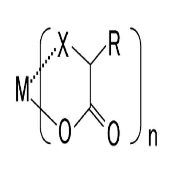
(M은 금속 이온이고, X는 NH2, OH, O, SH 중 적어도 하나이며, R은 수소(H) 또는 알킬 그룹(alkyl group)이고, n은 1 내지 3이다).
The method of claim 13,
Wherein the formula (1) comprises a compound represented by the following formula (2): < EMI ID =
(Wherein M is a metal ion, X is at least one of NH 2 , OH, O, and SH, R is a hydrogen (H) or an alkyl group, and n is 1 to 3).
상기 금속 이온은 Zinc(Zn), Tin(Sn), Indium(In), Galium(Ga), lithium(Li), sodium(Na), potassium(K), rubidium(Rb), cesium(Cs), beryllium(Be), aluminum(Al), barium(Ba), zirconium(Zr), hafnium(Hf), vanadium(V), yttrium(Y), niobium(Nb), tantalum(Ta), chromium(Cr), molybdenum(Mo), tungsten(W), manganese(Mn), technetium(Tc), rhenium(Re), iron(Fe), ruthenium(Ru), osmium(Os), cobalt(Co), rhodium(Rh), iridium(Ir), nickel(Ni), palladium(Pd), platinum(Pt), gold(Au), mercury(Hg), boron(B), thallium(Tl), silicon(Si), phosphorus(P), arsenic(As), lanthanum(La), cerium(Ce), gadolinium(Gd), Neodymiun(Nd), Tellurium(Te), Scandium(Sc), Polonium(Po), Praseodymiun(Pr), Terbium(Tb), Dysprosium(Dy), Holmium(Ho), Europium(Eu), Erbium(Er), 및 Ytterbium(Yb) 중에서 적어도 하나를 포함하는 박막 트랜지스터 표시판의 제조 방법.
16. The method of claim 15,
The metal ion may be selected from the group consisting of zinc (Zn), tin (Sn), indium (In), gallium (Ga), lithium (Li), sodium (Na), potassium (K), rubidium (Ba), zirconium (Zr), hafnium (Hf), vanadium (V), yttrium (Y), niobium (Nb), tantalum (Ta), chromium (Cr), molybdenum (Mo), tungsten (W), manganese (Mn), technetium (Tc), rhenium (Re), iron (Fe), ruthenium (Ru), osmium (Ir), nickel (Ni), palladium (Pd), platinum (Pt), gold (Au), mercury (Hg), boron (B), thallium (As), lanthanum (La), cerium (Ce), gadolinium (Gd), neodymium (Nd), tellurium (Te), Scandium (Sc), Polonium (Po), Praseodymium Wherein at least one selected from the group consisting of Dy, Holmium (Ho), Europium (Eu), Erbium (Er), and Ytterbium (Yb).
상기 금속 이온과 상기 유기 리간드의 몰 비율이 1:0.2 내지 1:10이 되도록 형성하는 박막 트랜지스터 표시판의 제조 방법.
17. The method of claim 16,
Wherein the molar ratio of the metal ion to the organic ligand is 1: 0.2 to 1:10.
Priority Applications (2)
| Application Number | Priority Date | Filing Date | Title |
|---|---|---|---|
| KR1020110025304A KR101850510B1 (en) | 2011-03-22 | 2011-03-22 | precursor composition for oxide semiconductor and manufacturing method of thin film transistor array panel using the same |
| US13/195,444 US8753920B2 (en) | 2011-03-22 | 2011-08-01 | Precursor composition for oxide semiconductor and method of manufacturing thin film transistor array panel using the same |
Applications Claiming Priority (1)
| Application Number | Priority Date | Filing Date | Title |
|---|---|---|---|
| KR1020110025304A KR101850510B1 (en) | 2011-03-22 | 2011-03-22 | precursor composition for oxide semiconductor and manufacturing method of thin film transistor array panel using the same |
Publications (2)
| Publication Number | Publication Date |
|---|---|
| KR20120107665A KR20120107665A (en) | 2012-10-04 |
| KR101850510B1 true KR101850510B1 (en) | 2018-04-20 |
Family
ID=46877678
Family Applications (1)
| Application Number | Title | Priority Date | Filing Date |
|---|---|---|---|
| KR1020110025304A Active KR101850510B1 (en) | 2011-03-22 | 2011-03-22 | precursor composition for oxide semiconductor and manufacturing method of thin film transistor array panel using the same |
Country Status (2)
| Country | Link |
|---|---|
| US (1) | US8753920B2 (en) |
| KR (1) | KR101850510B1 (en) |
Families Citing this family (12)
| Publication number | Priority date | Publication date | Assignee | Title |
|---|---|---|---|---|
| KR101884824B1 (en) * | 2011-09-07 | 2018-08-03 | 삼성디스플레이 주식회사 | Thin film transistor and manufacturing method thereof |
| KR20130089419A (en) * | 2012-02-02 | 2013-08-12 | 삼성디스플레이 주식회사 | Thin-film transistor substrate and method of manufacturing a thin-film transistor substrate |
| KR20130137851A (en) | 2012-06-08 | 2013-12-18 | 삼성디스플레이 주식회사 | Precursor composition for oxide semiconductor, thin film transistor array panel including oxide semiconductor, and manufacturing method of thin film transistor array panel including oxide semiconductor |
| WO2014077295A1 (en) * | 2012-11-15 | 2014-05-22 | Semiconductor Energy Laboratory Co., Ltd. | Liquid crystal display device |
| KR102198856B1 (en) | 2014-02-10 | 2021-01-05 | 삼성전자 주식회사 | Method of manufacturing semiconductor device including nickel-containing film |
| US9257638B2 (en) * | 2014-03-27 | 2016-02-09 | Lam Research Corporation | Method to etch non-volatile metal materials |
| CN105304571B (en) * | 2014-06-27 | 2018-02-13 | 旺宏电子股份有限公司 | Method for manufacturing memory device |
| US9070753B1 (en) * | 2014-07-09 | 2015-06-30 | Macronix International Co., Ltd. | Method for fabricating memory device |
| KR101759495B1 (en) * | 2015-08-21 | 2017-07-19 | 충북대학교 산학협력단 | Oxide Transistor and the controlling Method thereof |
| KR102084283B1 (en) * | 2015-12-16 | 2020-03-03 | 주식회사 엘지화학 | Composition for electric insulation material, electric insulation film manufactured by using the composition and circuit board and electronic device comprising the electric insulation film |
| KR20250010240A (en) * | 2023-07-12 | 2025-01-21 | 에스케이트리켐 주식회사 | High purity precursor comprising group 4 transtion metal and manufacturing method thereof |
| US20250305149A1 (en) * | 2024-03-28 | 2025-10-02 | Tokyo Electron Limited | Etching bi-metal oxides with alkaline earth metals |
Family Cites Families (18)
| Publication number | Priority date | Publication date | Assignee | Title |
|---|---|---|---|---|
| JPS6172071A (en) * | 1984-09-17 | 1986-04-14 | Yuuhoo Chem Kk | Coating agent composition |
| JP3229223B2 (en) * | 1995-10-13 | 2001-11-19 | キヤノン株式会社 | Method of manufacturing electron-emitting device, electron source and image forming apparatus, and metal composition for manufacturing electron-emitting device |
| JP2001244464A (en) | 2000-03-02 | 2001-09-07 | Sanyo Electric Works Ltd | Method for manufacturing metal oxide transistor |
| JP2003179242A (en) | 2001-12-12 | 2003-06-27 | National Institute Of Advanced Industrial & Technology | Metal oxide semiconductor thin film and method for producing the same |
| US7691666B2 (en) * | 2005-06-16 | 2010-04-06 | Eastman Kodak Company | Methods of making thin film transistors comprising zinc-oxide-based semiconductor materials and transistors made thereby |
| US7507618B2 (en) | 2005-06-27 | 2009-03-24 | 3M Innovative Properties Company | Method for making electronic devices using metal oxide nanoparticles |
| JP4258536B2 (en) * | 2006-08-11 | 2009-04-30 | 独立行政法人産業技術総合研究所 | Method for producing crystallized metal oxide thin film |
| US20080286907A1 (en) | 2007-05-16 | 2008-11-20 | Xerox Corporation | Semiconductor layer for thin film transistors |
| US20080296567A1 (en) | 2007-06-04 | 2008-12-04 | Irving Lyn M | Method of making thin film transistors comprising zinc-oxide-based semiconductor materials |
| US8834832B2 (en) * | 2007-12-21 | 2014-09-16 | 3M Innovative Properties Company | Process for producing nanoparticles |
| KR100960808B1 (en) | 2008-03-27 | 2010-05-31 | 연세대학교 산학협력단 | Oxide semiconductor thin film and its manufacturing method |
| JP2010010175A (en) | 2008-06-24 | 2010-01-14 | Konica Minolta Holdings Inc | Thin film transistor, and method of manufacturing thin film transistor |
| JP2010010549A (en) | 2008-06-30 | 2010-01-14 | Konica Minolta Holdings Inc | Method of manufacturing thin film transistor, and thin film transistor |
| JP2010171237A (en) | 2009-01-23 | 2010-08-05 | Konica Minolta Holdings Inc | Metal oxide semiconductor, method of manufacturing the same, and thin-film transistor using the same |
| JP2010182852A (en) | 2009-02-05 | 2010-08-19 | Konica Minolta Holdings Inc | Metal oxide semiconductor, manufacturing method therefor, and thin-film transistor |
| KR101664958B1 (en) | 2009-04-09 | 2016-10-12 | 삼성전자주식회사 | Solution composition for forming oxide thin film and electronic device including the oxide thin film |
| KR101069613B1 (en) * | 2009-09-04 | 2011-10-05 | 한국화학연구원 | Method to control a crystallization behavior for low temperature-processed and solution-processable oxide semiconductor |
| KR20110107130A (en) | 2010-03-24 | 2011-09-30 | 삼성전자주식회사 | Thin film transistor substrate and manufacturing method thereof |
-
2011
- 2011-03-22 KR KR1020110025304A patent/KR101850510B1/en active Active
- 2011-08-01 US US13/195,444 patent/US8753920B2/en active Active
Also Published As
| Publication number | Publication date |
|---|---|
| KR20120107665A (en) | 2012-10-04 |
| US8753920B2 (en) | 2014-06-17 |
| US20120244667A1 (en) | 2012-09-27 |
Similar Documents
| Publication | Publication Date | Title |
|---|---|---|
| KR101850510B1 (en) | precursor composition for oxide semiconductor and manufacturing method of thin film transistor array panel using the same | |
| US20110233536A1 (en) | Thin film transistor array panel and method of fabricating the same | |
| Bukke et al. | Lanthanum doping in zinc oxide for highly reliable thin-film transistors on flexible substrates by spray pyrolysis | |
| US9276129B2 (en) | Semiconductor device in which oxygen deficiency in semiconductor is reduced and method for manufacturing the same | |
| EP2786405B1 (en) | Coating liquid for forming metal oxide thin film and method for manufacturing field-effect transistor | |
| US9276123B2 (en) | Oxide semiconductor target and oxide semiconductor material, as well as semiconductor device using the same | |
| KR101910969B1 (en) | Composition for oxide semiconductor and method for manufacturing thin-film transistor substrate using the same | |
| TWI500165B (en) | Thin film transistor, manufacturing method thereof and electronic device | |
| US20100308326A1 (en) | Thin-film transistor array panel and method of fabricating the same | |
| KR102142038B1 (en) | Field effect transistor, manufacturing method thereof, display element, display device, and system | |
| US8373163B2 (en) | Oxide semiconductor and thin film transistor including the same | |
| US9082795B2 (en) | Precursor composition of oxide semiconductor and thin film transistor substrate including oxide semiconductor | |
| KR101406838B1 (en) | Oxide semiconductor and method of forming the same | |
| JP2021103791A (en) | Coating type semiconductor precursor solution, coating type oxide semiconductor, thin film transistor, and manufacturing method thereof | |
| KR101375846B1 (en) | Thin film transistor and mehtod for fabricating the same | |
| KR102135932B1 (en) | Thin film transistor array substrate for display device and method for fabricating the same | |
| US20130237011A1 (en) | Composition for oxide semiconductor and method of manufacturing a thin film transistor substrate using the same | |
| KR20150080947A (en) | Solution composition for fabricating oxide semiconductor and thin film transistor using the same | |
| KR102078991B1 (en) | Array Substrate Including Oxide Thin Film Transistor And Method Of Fabricating The Same | |
| US8895977B2 (en) | Thin film transistor and method of forming the same | |
| KR20150079331A (en) | Solution composition for fabricating oxide semiconductor and thin film transistor using the same |
Legal Events
| Date | Code | Title | Description |
|---|---|---|---|
| PA0109 | Patent application |
St.27 status event code: A-0-1-A10-A12-nap-PA0109 |
|
| R18-X000 | Changes to party contact information recorded |
St.27 status event code: A-3-3-R10-R18-oth-X000 |
|
| N231 | Notification of change of applicant | ||
| PN2301 | Change of applicant |
St.27 status event code: A-3-3-R10-R13-asn-PN2301 St.27 status event code: A-3-3-R10-R11-asn-PN2301 |
|
| PG1501 | Laying open of application |
St.27 status event code: A-1-1-Q10-Q12-nap-PG1501 |
|
| R18-X000 | Changes to party contact information recorded |
St.27 status event code: A-3-3-R10-R18-oth-X000 |
|
| A201 | Request for examination | ||
| E13-X000 | Pre-grant limitation requested |
St.27 status event code: A-2-3-E10-E13-lim-X000 |
|
| P11-X000 | Amendment of application requested |
St.27 status event code: A-2-2-P10-P11-nap-X000 |
|
| P13-X000 | Application amended |
St.27 status event code: A-2-2-P10-P13-nap-X000 |
|
| PA0201 | Request for examination |
St.27 status event code: A-1-2-D10-D11-exm-PA0201 |
|
| D13-X000 | Search requested |
St.27 status event code: A-1-2-D10-D13-srh-X000 |
|
| D14-X000 | Search report completed |
St.27 status event code: A-1-2-D10-D14-srh-X000 |
|
| E902 | Notification of reason for refusal | ||
| PE0902 | Notice of grounds for rejection |
St.27 status event code: A-1-2-D10-D21-exm-PE0902 |
|
| E13-X000 | Pre-grant limitation requested |
St.27 status event code: A-2-3-E10-E13-lim-X000 |
|
| P11-X000 | Amendment of application requested |
St.27 status event code: A-2-2-P10-P11-nap-X000 |
|
| P13-X000 | Application amended |
St.27 status event code: A-2-2-P10-P13-nap-X000 |
|
| E701 | Decision to grant or registration of patent right | ||
| PE0701 | Decision of registration |
St.27 status event code: A-1-2-D10-D22-exm-PE0701 |
|
| PR0701 | Registration of establishment |
St.27 status event code: A-2-4-F10-F11-exm-PR0701 |
|
| PR1002 | Payment of registration fee |
St.27 status event code: A-2-2-U10-U11-oth-PR1002 Fee payment year number: 1 |
|
| PG1601 | Publication of registration |
St.27 status event code: A-4-4-Q10-Q13-nap-PG1601 |
|
| R18-X000 | Changes to party contact information recorded |
St.27 status event code: A-5-5-R10-R18-oth-X000 |
|
| PR1001 | Payment of annual fee |
St.27 status event code: A-4-4-U10-U11-oth-PR1001 Fee payment year number: 4 |
|
| PR1001 | Payment of annual fee |
St.27 status event code: A-4-4-U10-U11-oth-PR1001 Fee payment year number: 5 |
|
| PR1001 | Payment of annual fee |
St.27 status event code: A-4-4-U10-U11-oth-PR1001 Fee payment year number: 6 |
|
| PR1001 | Payment of annual fee |
St.27 status event code: A-4-4-U10-U11-oth-PR1001 Fee payment year number: 7 |
|
| P22-X000 | Classification modified |
St.27 status event code: A-4-4-P10-P22-nap-X000 |
|
| PR1001 | Payment of annual fee |
St.27 status event code: A-4-4-U10-U11-oth-PR1001 Fee payment year number: 8 |
|
| P22-X000 | Classification modified |
St.27 status event code: A-4-4-P10-P22-nap-X000 |