KR101811642B1 - Method of driving liquid crystal lens, liquid crystal module for performing the same and display apparatus having the same - Google Patents
Method of driving liquid crystal lens, liquid crystal module for performing the same and display apparatus having the same Download PDFInfo
- Publication number
- KR101811642B1 KR101811642B1 KR1020110030267A KR20110030267A KR101811642B1 KR 101811642 B1 KR101811642 B1 KR 101811642B1 KR 1020110030267 A KR1020110030267 A KR 1020110030267A KR 20110030267 A KR20110030267 A KR 20110030267A KR 101811642 B1 KR101811642 B1 KR 101811642B1
- Authority
- KR
- South Korea
- Prior art keywords
- lens
- voltage
- driving
- liquid crystal
- unit
- Prior art date
- Legal status (The legal status is an assumption and is not a legal conclusion. Google has not performed a legal analysis and makes no representation as to the accuracy of the status listed.)
- Expired - Fee Related
Links
Images


Classifications
-
- G—PHYSICS
- G02—OPTICS
- G02F—OPTICAL DEVICES OR ARRANGEMENTS FOR THE CONTROL OF LIGHT BY MODIFICATION OF THE OPTICAL PROPERTIES OF THE MEDIA OF THE ELEMENTS INVOLVED THEREIN; NON-LINEAR OPTICS; FREQUENCY-CHANGING OF LIGHT; OPTICAL LOGIC ELEMENTS; OPTICAL ANALOGUE/DIGITAL CONVERTERS
- G02F1/00—Devices or arrangements for the control of the intensity, colour, phase, polarisation or direction of light arriving from an independent light source, e.g. switching, gating or modulating; Non-linear optics
- G02F1/01—Devices or arrangements for the control of the intensity, colour, phase, polarisation or direction of light arriving from an independent light source, e.g. switching, gating or modulating; Non-linear optics for the control of the intensity, phase, polarisation or colour
- G02F1/13—Devices or arrangements for the control of the intensity, colour, phase, polarisation or direction of light arriving from an independent light source, e.g. switching, gating or modulating; Non-linear optics for the control of the intensity, phase, polarisation or colour based on liquid crystals, e.g. single liquid crystal display cells
- G02F1/133—Constructional arrangements; Operation of liquid crystal cells; Circuit arrangements
- G02F1/13306—Circuit arrangements or driving methods for the control of single liquid crystal cells
-
- H—ELECTRICITY
- H04—ELECTRIC COMMUNICATION TECHNIQUE
- H04N—PICTORIAL COMMUNICATION, e.g. TELEVISION
- H04N13/00—Stereoscopic video systems; Multi-view video systems; Details thereof
- H04N13/30—Image reproducers
- H04N13/302—Image reproducers for viewing without the aid of special glasses, i.e. using autostereoscopic displays
- H04N13/305—Image reproducers for viewing without the aid of special glasses, i.e. using autostereoscopic displays using lenticular lenses, e.g. arrangements of cylindrical lenses
-
- H—ELECTRICITY
- H04—ELECTRIC COMMUNICATION TECHNIQUE
- H04N—PICTORIAL COMMUNICATION, e.g. TELEVISION
- H04N13/00—Stereoscopic video systems; Multi-view video systems; Details thereof
- H04N13/30—Image reproducers
- H04N13/302—Image reproducers for viewing without the aid of special glasses, i.e. using autostereoscopic displays
- H04N13/317—Image reproducers for viewing without the aid of special glasses, i.e. using autostereoscopic displays using slanted parallax optics
-
- H—ELECTRICITY
- H04—ELECTRIC COMMUNICATION TECHNIQUE
- H04N—PICTORIAL COMMUNICATION, e.g. TELEVISION
- H04N13/00—Stereoscopic video systems; Multi-view video systems; Details thereof
- H04N13/30—Image reproducers
- H04N13/356—Image reproducers having separate monoscopic and stereoscopic modes
- H04N13/359—Switching between monoscopic and stereoscopic modes
-
- G—PHYSICS
- G02—OPTICS
- G02F—OPTICAL DEVICES OR ARRANGEMENTS FOR THE CONTROL OF LIGHT BY MODIFICATION OF THE OPTICAL PROPERTIES OF THE MEDIA OF THE ELEMENTS INVOLVED THEREIN; NON-LINEAR OPTICS; FREQUENCY-CHANGING OF LIGHT; OPTICAL LOGIC ELEMENTS; OPTICAL ANALOGUE/DIGITAL CONVERTERS
- G02F1/00—Devices or arrangements for the control of the intensity, colour, phase, polarisation or direction of light arriving from an independent light source, e.g. switching, gating or modulating; Non-linear optics
- G02F1/01—Devices or arrangements for the control of the intensity, colour, phase, polarisation or direction of light arriving from an independent light source, e.g. switching, gating or modulating; Non-linear optics for the control of the intensity, phase, polarisation or colour
- G02F1/13—Devices or arrangements for the control of the intensity, colour, phase, polarisation or direction of light arriving from an independent light source, e.g. switching, gating or modulating; Non-linear optics for the control of the intensity, phase, polarisation or colour based on liquid crystals, e.g. single liquid crystal display cells
- G02F1/133—Constructional arrangements; Operation of liquid crystal cells; Circuit arrangements
- G02F1/1333—Constructional arrangements; Manufacturing methods
- G02F1/1347—Arrangement of liquid crystal layers or cells in which the final condition of one light beam is achieved by the addition of the effects of two or more layers or cells
- G02F1/13471—Arrangement of liquid crystal layers or cells in which the final condition of one light beam is achieved by the addition of the effects of two or more layers or cells in which all the liquid crystal cells or layers remain transparent, e.g. FLC, ECB, DAP, HAN, TN, STN, SBE-LC cells
Landscapes
- Physics & Mathematics (AREA)
- Engineering & Computer Science (AREA)
- Multimedia (AREA)
- Signal Processing (AREA)
- Nonlinear Science (AREA)
- Optics & Photonics (AREA)
- Mathematical Physics (AREA)
- Chemical & Material Sciences (AREA)
- Crystallography & Structural Chemistry (AREA)
- General Physics & Mathematics (AREA)
- Liquid Crystal (AREA)
- Testing, Inspecting, Measuring Of Stereoscopic Televisions And Televisions (AREA)
Abstract
액정 렌즈의 구동 방법은 2차원 모드 및 3차원 모드를 포함하는 구동 모드를 판단하는 단계 및 3차원 모드에서 복수의 단위 렌즈들을 포함하는 액정 렌즈의 단위 렌즈들을 서로 다른 타이밍으로 구동하는 단계를 포함한다. 이에 따라, 2차원 영상 및 3차원 영상을 효과적으로 표시할 수 있다.The driving method of the liquid crystal lens includes determining a driving mode including a two-dimensional mode and a three-dimensional mode, and driving the unit lenses of the liquid crystal lens including a plurality of unit lenses at different timings in a three-dimensional mode . Accordingly, the two-dimensional image and the three-dimensional image can be displayed effectively.
Description
본 발명은 액정 렌즈의 구동 방법, 이를 수행하기 위한 액정 렌즈 모듈 및 이를 포함하는 표시 장치에 관한 것으로, 더욱 상세하게는 2차원 영상 및 3차원 영상을 표시하기 위한 액정 렌즈의 구동 방법, 이를 수행하기 위한 액정 렌즈 모듈 및 이를 포함하는 표시 장치에 관한 것이다.The present invention relates to a liquid crystal lens driving method, a liquid crystal lens module for performing the same, and a display device including the liquid crystal lens module. More particularly, the present invention relates to a liquid crystal lens driving method for displaying a two- And a display device including the liquid crystal lens module.
일반적으로 액정 표시 장치는 2차원 영상을 표시한다. 최근 게임, 영화 등과 같은 분야에서 3차원 영상에 대한 수요가 증가함에 따라, 상기 액정 표시 장치를 이용하여 3차원 영상을 표시한다.In general, a liquid crystal display device displays a two-dimensional image. Recently, as the demand for three-dimensional images in the fields such as games, movies, and the like increases, a three-dimensional image is displayed using the liquid crystal display device.
일반적으로, 사람의 두 눈을 통한 양안시차(binocular parallax)의 원리를 이용하여 입체 영상을 표시할 수 있다. 예를 들어, 사람의 두 눈은 일정 정도 떨어져 존재하기 때문에 각각의 눈으로 다른 각도에서 관찰한 영상은 뇌에 입력된다.Generally, stereoscopic images can be displayed using the principle of binocular parallax through two eyes of a person. For example, since two eyes of a person are separated by a certain degree, images observed from different angles with each eye are input to the brain.
상기 양안시차를 이용하는 방식으로는, 안경 방식(stereoscopic)과 비안경 방식(autostereoscopic)이 있다. 상기 안경 방식은 애너그러프(anaglyph) 방식 및 셔터 안경(Shutter Glass) 방식 등이 있다. 상기 비안경 방식은 배리어 방식, 렌티큘라(lenticular) 방식 및 액정 렌즈 방식 등이 있다.Examples of the binocular parallax method include a stereoscopic method and an autostereoscopic method. The above-mentioned glasses system includes an anaglyph system and a shutter glasses system. The non-spectacle method includes a barrier method, a lenticular method, and a liquid crystal lens method.
상기 액정 렌즈 방식에서는 액정 패널을 이용하여 광을 굴절시키는 렌즈를 구현한다. 액정 렌즈는 렌즈 전극을 포함하는 제1 기판, 상기 제1 기판과 대향하며 공통 전극을 포함하는 제2 기판 및 상기 제1 및 제2 기판들 사이에 개제되는 액정층을 포함한다. 상기 액정 패널의 상기 제1 및 제2 기판들에 전압을 인가하면 상기 액정층의 액정 분자들의 배열이 조절된다. 상기 액정 분자들의 배열을 적절히 조절하면 상기 액정 패널은 렌즈의 기능을 할 수 있다.In the liquid crystal lens system, a lens for refracting light using a liquid crystal panel is implemented. The liquid crystal lens includes a first substrate including a lens electrode, a second substrate facing the first substrate and including a common electrode, and a liquid crystal layer interposed between the first and second substrates. When a voltage is applied to the first and second substrates of the liquid crystal panel, the arrangement of the liquid crystal molecules in the liquid crystal layer is adjusted. When the arrangement of the liquid crystal molecules is appropriately adjusted, the liquid crystal panel can function as a lens.
상기 액정 렌즈의 대형화 추세에 따라, 상기 렌즈 전극 및 공통 전극의 응답 시간 지연, 상기 렌즈 전극 및 공통 전극 간의 커플링 현상 등이 발생하는 문제점이 있다. 또한, 상기 렌즈 전극들에 인가되는 구동 전류가 증가하는 문제점 등이 있다.There is a problem in that response time delay of the lens electrode and the common electrode and coupling phenomenon between the lens electrode and the common electrode occur in accordance with the tendency of the liquid crystal lens to become larger. In addition, there is a problem that the driving current applied to the lens electrodes increases.
이에, 본 발명의 기술적 과제는 이러한 점에서 착안된 것으로 본 발명의 목적은 2차원 영상 및 3차원 영상을 효과적으로 표시하기 위한 액정 렌즈의 구동 방법을 제공하는 것이다.Accordingly, it is an object of the present invention to provide a method of driving a liquid crystal lens for effectively displaying a two-dimensional image and a three-dimensional image.
본 발명의 다른 목적은 상기 액정 렌즈의 구동 방법을 수행하는 데에 적합한 액정 렌즈 모듈을 제공하는 것이다.Another object of the present invention is to provide a liquid crystal lens module suitable for performing the driving method of the liquid crystal lens.
본 발명의 또 다른 목적은 상기 액정 렌즈 모듈을 포함하는 표시 장치를 제공하는 것이다.It is still another object of the present invention to provide a display device including the liquid crystal lens module.
상기한 본 발명의 목적을 실현하기 위한 일 실시예에 따른 액정 렌즈의 구동 방법은 2차원 모드 및 3차원 모드를 포함하는 구동 모드를 판단하는 단계 및 상기 3차원 모드에서 복수의 단위 렌즈들을 포함하는 액정 렌즈의 상기 단위 렌즈들을 서로 다른 타이밍으로 구동하는 단계를 포함한다.According to another aspect of the present invention, there is provided a method of driving a liquid crystal lens, including: determining a driving mode including a two-dimensional mode and a three-dimensional mode; And driving the unit lenses of the liquid crystal lens at different timings.
본 발명의 일 실시예에 있어서, 상기 단위 렌즈들을 구동하는 단계는 서로 다른 타이밍을 갖는 렌즈 제어 신호들을 생성하는 단계 및 상기 렌즈 제어 신호들을 복수의 렌즈 전극들과 연결되는 각각의 렌즈 구동 칩들에 출력하는 단계를 포함할 수 있다.In one embodiment of the present invention, driving the unit lenses includes generating lens control signals having different timings, and outputting the lens control signals to respective lens driving chips connected to the plurality of lens electrodes .
본 발명의 일 실시예에 있어서, 상기 단위 렌즈들을 구동하는 단계는 렌즈 전극의 제1 단에 렌즈 전압을 출력하고, 상기 렌즈 전극의 상기 제1 단에 반대되는 제2 단에 렌즈 전압을 출력할 수 있다.In one embodiment of the present invention, the step of driving the unit lenses may include outputting a lens voltage to a first end of the lens electrode, and outputting a lens voltage to a second end of the lens electrode opposite to the first end .
본 발명의 일 실시예에 있어서, 상기 단위 렌즈들을 구동하는 단계는 공통 전압을 생성하는 단계 및 상기 공통 전압을 공통 전극에 출력하는 단계를 더 포함할 수 있다. 상기 공통 전압을 생성하는 단계는 제1 전압, 제2 전압 및 제3 전압을 선택할 수 있다.In one embodiment of the present invention, driving the unit lenses may further include generating a common voltage and outputting the common voltage to the common electrode. The generating of the common voltage may select a first voltage, a second voltage, and a third voltage.
본 발명의 일 실시예에 있어서, 상기 공통 전압을 생성하는 단계는 입력 영상 데이터의 수직 동기 신호 및 반전 신호를 이용하여 상기 제1, 제2 및 제3 전압들을 선택할 수 있다.In one embodiment of the present invention, the generating of the common voltage may select the first, second, and third voltages using a vertical synchronizing signal and an inverting signal of the input image data.
본 발명의 일 실시예에 있어서, 상기 제1 전압은 정상 상태의 공통 전압이고, 상기 제2 전압은 상기 제1 전압보다 크며, 상기 제3 전압은 상기 제1 전압보다 작을 수 있다. 상기 제2 전압은 렌즈 전극에 인가되는 렌즈 전압의 폴링 에지에서 출력될 수 있다. 상기 제3 전압은 상기 렌즈 전압의 라이징 에지에서 출력될 수 있다.In one embodiment of the present invention, the first voltage is a steady state common voltage, the second voltage is greater than the first voltage, and the third voltage may be less than the first voltage. The second voltage may be output at the falling edge of the lens voltage applied to the lens electrode. The third voltage may be output at the rising edge of the lens voltage.
본 발명의 일 실시예에 있어서, 상기 액정 렌즈의 구동 방법은 상기 구동 모드에 따라 광원 구동 전압의 레벨을 선택적으로 생성하는 단계를 더 포함할 수 있다.According to an embodiment of the present invention, the driving method of the liquid crystal lens may further include selectively generating a level of the light source driving voltage according to the driving mode.
본 발명의 일 실시예에 있어서, 상기 3차원 모드의 상기 광원 구동 전압은 상기 2차원 모드의 광원 구동 전압보다 클 수 있다.In one embodiment of the present invention, the light source driving voltage in the three-dimensional mode may be greater than the light source driving voltage in the two-dimensional mode.
본 발명의 일 실시예에 있어서, 상기 단위 렌즈들을 구동하는 단계는 공통 전압을 생성하는 단계 및 상기 공통 전압을 공통 전극에 출력하는 단계를 더 포함할 수 있다. 상기 2차원 모드에서 상기 공통 전압을 0V로 설정할 수 있다.In one embodiment of the present invention, driving the unit lenses may further include generating a common voltage and outputting the common voltage to the common electrode. The common voltage can be set to 0 V in the two-dimensional mode.
상기한 본 발명의 다른 목적을 실현하기 위한 일 실시예에 따른 액정 렌즈 모듈은 액정 렌즈 및 제어부를 포함한다. 상기 액정 렌즈는 복수의 렌즈 전극들을 포함하는 제1 기판, 공통 전극을 포함하는 제2 기판, 및 상기 제1 및 제2 기판들 사이에 개제된 액정층에 의해 형성되는 복수의 단위 렌즈들을 포함한다. 상기 제어부는 2차원 모드 및 3차원 모드를 포함하는 구동 모드를 판단한다. 상기 제어부는 상기 3차원 모드에서 상기 단위 렌즈들을 서로 다른 타이밍으로 구동한다.According to another aspect of the present invention, a liquid crystal lens module includes a liquid crystal lens and a control unit. The liquid crystal lens includes a first substrate including a plurality of lens electrodes, a second substrate including a common electrode, and a plurality of unit lenses formed by a liquid crystal layer interposed between the first and second substrates . The controller determines a driving mode including a two-dimensional mode and a three-dimensional mode. The control unit drives the unit lenses at different timings in the three-dimensional mode.
본 발명의 일 실시예에 있어서, 상기 제어부는 서로 다른 타이밍을 갖는 렌즈 제어 신호들을 생성할 수 있다. 상기 제어부는 상기 렌즈 제어 신호들을 상기 렌즈 전극들과 연결되는 각각의 렌즈 구동 칩들에 출력할 수 있다.In an embodiment of the present invention, the controller may generate lens control signals having different timings. The control unit may output the lens control signals to the lens driving chips connected to the lens electrodes.
본 발명의 일 실시예에 있어서, 상기 액정 렌즈 모듈은 상기 제1 기판의 제1 변에 인접하여 배치되는 제1 렌즈 구동부 및 상기 제1 기판의 제2 변에 인접하여 배치되는 제2 렌즈 구동부를 더 포함할 수 있다. 상기 제1 렌즈 구동부는 상기 렌즈 전극의 제1 단에 렌즈 전압을 출력하고, 상기 제2 렌즈 구동부는 상기 렌즈 전극의 상기 제1 단에 반대되는 제2 단에 렌즈 전압을 출력할 수 있다.In one embodiment of the present invention, the liquid crystal lens module includes a first lens driving unit disposed adjacent to a first side of the first substrate, and a second lens driving unit disposed adjacent to a second side of the first substrate, . The first lens driving unit outputs a lens voltage to a first end of the lens electrode and the second lens driving unit outputs a lens voltage to a second end opposite to the first end of the lens electrode.
본 발명의 일 실시예에 있어서, 상기 제어부는 공통 전압을 생성하여 상기 공통 전극에 출력할 수 있다. 상기 공통 전압은 제1 전압, 제2 전압 및 제3 전압 중 선택적으로 생성될 수 있다.In one embodiment of the present invention, the control unit may generate a common voltage and output the common voltage to the common electrode. The common voltage may be selectively generated among a first voltage, a second voltage, and a third voltage.
본 발명의 일 실시예에 있어서, 상기 제어부는 입력 영상 데이터의 수직 동기 신호 및 반전 신호를 이용하여 상기 제1, 제2 및 제3 전압들을 선택할 수 있다.In one embodiment of the present invention, the controller may select the first, second, and third voltages using a vertical synchronization signal and an inversion signal of the input image data.
본 발명의 일 실시예에 있어서, 상기 제1 전압은 정상 상태의 공통 전압이고, 상기 제2 전압은 상기 제1 전압보다 크며, 상기 제3 전압은 상기 제1 전압보다 작을 수 있다. 상기 제2 전압은 상기 렌즈 전극에 인가되는 렌즈 전압의 폴링 에지에서 출력될 수 있다. 상기 제3 전압은 상기 렌즈 전압의 라이징 에지에서 출력될 수 있다.In one embodiment of the present invention, the first voltage is a steady state common voltage, the second voltage is greater than the first voltage, and the third voltage may be less than the first voltage. The second voltage may be output at the falling edge of the lens voltage applied to the lens electrode. The third voltage may be output at the rising edge of the lens voltage.
본 발명의 일 실시예에 있어서, 상기 제어부는 상기 구동 모드에 따라 광원 구동 전압의 레벨을 선택적으로 결정하는 디밍부를 포함할 수 있다.In one embodiment of the present invention, the controller may include a dimming unit for selectively determining a level of the light source driving voltage according to the driving mode.
본 발명의 일 실시예에 있어서, 상기 3차원 모드의 상기 광원 구동 전압은 상기 2차원 모드의 광원 구동 전압보다 클 수 있다.In one embodiment of the present invention, the light source driving voltage in the three-dimensional mode may be greater than the light source driving voltage in the two-dimensional mode.
본 발명의 일 실시예에 있어서, 상기 제어부는 공통 전압을 생성하여 상기 공통 전극에 출력할 수 있다. 상기 2차원 모드에서 상기 공통 전압을 0V로 설정할 수 있다.In one embodiment of the present invention, the control unit may generate a common voltage and output the common voltage to the common electrode. The common voltage can be set to 0 V in the two-dimensional mode.
상기한 본 발명의 또 다른 목적을 실현하기 위한 일 실시예에 따른 표시 장치는 표시 패널, 광원부, 액정 렌즈 및 제어부를 포함한다. 상기 표시 패널은 영상을 표시한다. 상기 광원부는 상기 표시 패널에 광을 공급한다. 상기 액정 렌즈는 상기 표시 패널 상에 배치된다. 상기 액정 렌즈는 복수의 렌즈 전극들을 포함하는 제1 기판, 공통 전극을 포함하는 제2 기판, 및 상기 제1 및 제2 기판들 사이에 개제된 액정층에 의해 형성되는 복수의 단위 렌즈들을 포함한다. 상기 제어부는 2차원 모드 및 3차원 모드를 포함하는 구동 모드를 판단한다. 상기 제어부는 상기 3차원 모드에서 상기 단위 렌즈들을 서로 다른 타이밍으로 구동한다.According to another aspect of the present invention, a display device includes a display panel, a light source, a liquid crystal lens, and a control unit. The display panel displays an image. The light source supplies light to the display panel. The liquid crystal lens is disposed on the display panel. The liquid crystal lens includes a first substrate including a plurality of lens electrodes, a second substrate including a common electrode, and a plurality of unit lenses formed by a liquid crystal layer interposed between the first and second substrates . The controller determines a driving mode including a two-dimensional mode and a three-dimensional mode. The control unit drives the unit lenses at different timings in the three-dimensional mode.
본 발명의 일 실시예에 있어서, 상기 제어부는 서로 다른 타이밍을 갖는 렌즈 제어 신호들을 생성할 수 있다. 상기 제어부는 상기 렌즈 제어 신호들을 상기 렌즈 전극들과 연결되는 각각의 렌즈 구동 칩들에 출력할 수 있다.In an embodiment of the present invention, the controller may generate lens control signals having different timings. The control unit may output the lens control signals to the lens driving chips connected to the lens electrodes.
이와 같은 액정 렌즈의 구동 방법, 이를 수행하기 위한 액정 렌즈 모듈 및 이를 포함하는 표시 장치에 따르면, 2차원 영상 및 3차원 영상을 효과적으로 표시할 수 있다.According to the liquid crystal lens driving method, the liquid crystal lens module for performing the method, and the display device including the liquid crystal lens module, the two-dimensional image and the three-dimensional image can be displayed effectively.
도 1은 본 발명의 일 실시예에 따른 표시 장치를 나타내는 블록도이다.
도 2는 도 1의 표시 장치를 나타내는 분해 사시도이다.
도 3은 도 1의 액정 렌즈의 제1 기판 및 렌즈 구동부를 나타내는 평면도이다.
도 4는 도 1의 제어부를 나타내는 블록도이다.
도 5는 도 4의 제1 렌즈 제어부를 나타내는 블록도이다.
도 6은 도 3의 제1 서브 구동 칩을 나타내는 블록도이다.
도 7은 도 5의 신호 생성부에서 생성되는 렌즈 제어 신호 및 도 5의 전원 생성부에서 생성되는 렌즈 전원 전류를 나타내는 파형도이다.
도 8은 도 5의 공통 전압 생성부의 동작을 나타내는 개념도이다.
도 9는 도 2의 렌즈 구동 칩에서 출력되는 렌즈 전압 및 도 5의 공통 전압 생성부에서 생성되는 공통 전압을 나타내는 파형도이다.
도 10은 도 4의 디밍부의 동작을 나타내는 개념도이다.
도 11은 도 5의 공통 전압 생성부 및 상기 공통 전압 생성부에 연결되는 공통 전압 차단부를 나타내는 블록도이다.
도 12는 도 11의 공통 전압 차단부의 동작을 나타내는 개념도이다.
도 13은 도 4의 영상 처리부에서 판단되는 구동 모드, 도 2의 렌즈 구동 칩에서 출력되는 렌즈 전압 및 도 11의 공통 전압 차단부를 통과하는 공통 전압을 나타내는 파형도이다.1 is a block diagram showing a display device according to an embodiment of the present invention.
2 is an exploded perspective view showing the display device of FIG.
3 is a plan view showing the first substrate and the lens driving unit of the liquid crystal lens of FIG.
4 is a block diagram showing the control unit of Fig.
5 is a block diagram showing the first lens control unit of FIG.
FIG. 6 is a block diagram showing the first sub-drive chip of FIG. 3. FIG.
FIG. 7 is a waveform diagram showing a lens control signal generated by the signal generator of FIG. 5 and a lens power supply current generated by the power generator of FIG. 5;
8 is a conceptual diagram showing the operation of the common voltage generator of FIG.
FIG. 9 is a waveform diagram showing a lens voltage output from the lens driving chip of FIG. 2 and a common voltage generated by the common voltage generator of FIG. 5;
10 is a conceptual diagram showing the operation of the dimming unit of FIG.
11 is a block diagram showing a common voltage generating unit of FIG. 5 and a common voltage blocking unit connected to the common voltage generating unit.
12 is a conceptual diagram showing the operation of the common voltage interrupter of FIG.
FIG. 13 is a waveform diagram showing a driving mode judged by the image processing unit of FIG. 4, a lens voltage output from the lens driving chip of FIG. 2, and a common voltage passing through the common voltage blocking unit of FIG.
이하, 첨부한 도면들을 참조하여, 본 발명을 보다 상세하게 설명하고자 한다.DETAILED DESCRIPTION OF THE PREFERRED EMBODIMENTS The present invention will now be described in more detail with reference to the accompanying drawings.
도 1은 본 발명의 일 실시예에 따른 표시 장치를 나타내는 블록도이다. 도 2는 도 1의 표시 장치를 나타내는 분해 사시도이다.1 is a block diagram showing a display device according to an embodiment of the present invention. 2 is an exploded perspective view showing the display device of FIG.
도 1 및 도 2를 참조하면, 상기 표시 장치는 광원 모듈, 표시 패널 모듈 및 액정 렌즈 모듈을 포함한다. 상기 광원 모듈은 광원부(100), 광원 제어부 및 광원 구동부(500)를 포함한다. 상기 표시 패널 모듈은 표시 패널(200), 패널 제어부 및 패널 구동부(600)를 포함한다. 상기 액정 렌즈 모듈은 액정 렌즈(300), 렌즈 제어부 및 렌즈 구동부(700)를 포함한다.1 and 2, the display device includes a light source module, a display panel module, and a liquid crystal lens module. The light source module includes a
상기 표시 장치는 광원부(100), 표시 패널(200), 액정 렌즈(300), 제어부(400), 광원 구동부(500), 패널 구동부(600) 및 렌즈 구동부(700)를 포함한다.The display device includes a
상기 광원부(100)는 상기 표시 패널(200)에 광을 제공한다. 상기 광원부(100)는 광을 발생시키는 광원을 포함한다. 예를 들어, 상기 광원은 냉음극 형광램프(cold cathode fluorescent lamp, CCFL), 외부전극 형광램프(external electrode fluorescent lamp, EEFL), 평판 형광램프(flat fluorescent lamp, FFL), 발광 다이오드(light emitting diode, LED)를 포함할 수 있다. 상기 광원부(100)는 백라이트 어셈블리일 수 있다.The
상기 광원부(100)는 상기 표시 패널(200)의 하부에 배치되어, 상기 표시 패널(200)로 광을 제공하는 직하형 광원부일 수 있다. 상기 광원부(100)는 상기 표시 패널(200)의 측변에 대응하게 배치되어, 표시 패널(200)로 광을 제공하는 에지형 광원부일 수 있다. 상기 광원부(100)가 에지형 광원부인 경우 상기 광원부(100)는 도광판(미도시)을 더 포함할 수 있다.The
상기 표시 패널(200)은 상기 광원부(100) 상에 배치된다. 상기 표시 패널(200)은 제1 패널 기판(210) 및 제2 패널 기판(220)을 포함한다. 상기 제1 및 제2 패널 기판들(210, 220) 사이에는 액정층(미도시)이 개제된다.The
상기 표시 패널(200)은 복수의 게이트 배선들(미도시), 복수의 데이터 배선들(미도시) 및 상기 게이트 배선들과 상기 데이터 배선들 각각에 연결되는 복수의 화소들(미도시)을 포함한다.The
각 화소는 스위칭 소자(미도시), 상기 스위칭 소자에 전기적으로 연결된 액정 캐패시터(미도시) 및 스토리지 캐패시터(미도시)를 포함한다.Each pixel includes a switching element (not shown), a liquid crystal capacitor (not shown) electrically connected to the switching element, and a storage capacitor (not shown).
상기 제1 패널 기판(210) 상에 상기 게이트 배선들, 상기 데이터 배선들, 화소 전극들(미도시), 스토리지 전극들(미도시)이 배치되고, 상기 제2 패널 기판(220) 상에 공통 전극(미도시)이 배치될 수 있다.The gate lines, the data lines, the pixel electrodes (not shown), and the storage electrodes (not shown) are disposed on the first panel substrate 210, An electrode (not shown) may be disposed.
상기 표시 패널(200)은 2차원 모드에서 2차원 영상을 표시할 수 있다. 상기 표시 패널(200)은 3차원 모드에서 3차원 영상을 표시할 수 있다.The
상기 액정 렌즈(300)는 상기 표시 패널(200) 상에 배치된다. 상기 액정 렌즈(300)는 제1 기판(310) 및 제2 기판(320)을 포함한다. 상기 제1 및 제2 기판들(310, 320) 사이에는 액정층(미도시)이 개제된다.The
상기 액정 렌즈(300)는 복수의 단위 렌즈들을 포함한다. 상기 단위 렌즈들은 제1 방향(D1)을 따라 배치된다. 각각의 단위 렌즈들은 상기 제1 방향(D1)과 교차하는 제2 방향(D2)을 따라 연장된다. 상기 단위 렌즈들은 상기 제2 방향(D2)으로부터 일정 각도로 기울어져 연장될 수 있다.The
상기 제1 기판(310) 상에는 복수의 렌즈 전극들이 배치된다. 상기 제2 기판(320) 상에는 공통 전극이 배치된다.A plurality of lens electrodes are disposed on the
상기 렌즈 전극들 및 상기 공통 전극은 인듐 아연 산화물(Indium Zinc Oxide, IZO)을 포함할 수 있다.The lens electrodes and the common electrode may include indium zinc oxide (IZO).
상기 렌즈 전극들 및 상기 공통 전극에 구동 전압이 인가되면, 상기 액정층의 액정 분자들의 배열이 조절되어 상기 액정 렌즈(300)는 렌즈의 굴절률 분포를 갖는다.When a drive voltage is applied to the lens electrodes and the common electrode, the arrangement of the liquid crystal molecules in the liquid crystal layer is adjusted so that the
상기 액정 렌즈(300)는 2차원 모드 또는 3차원 모드로 구동된다. 예를 들면, 상기 2차원 모드에서 상기 액정 렌즈(300)는 상기 표시 패널(200)로부터 제공된 영상을 굴절 없이 그대로 통과시킨다. 따라서, 관찰자는 2차원 영상을 시인한다.The
상기 3차원 모드에서 상기 액정 렌즈(300)는 렌즈로 동작하여 상기 표시 패널(200)로부터 제공된 영상을 굴절시키다. 따라서, 관찰자는 3차원 영상을 시인한다.In the three-dimensional mode, the
상기 제어부(400)는 외부로부터 입력 영상 데이터, 입력 렌즈 데이터 및 입력 제어 신호를 수신한다.The
상기 입력 영상 데이터는 2차원 영상 데이터 및 3차원 영상 데이터를 포함할 수 있다. 상기 입력 영상 데이터는 적색 영상 데이터, 녹색 영상 데이터 및 청색 영상 데이터를 포함할 수 있다. 상기 입력 렌즈 데이터는 상기 액정 렌즈(300)의 굴절률을 나타내기 위해 상기 렌즈 전극들에 제공되는 전압일 수 있다. 상기 입력 제어 신호는 마스터 클럭 신호, 수직 동기 신호, 반전 신호 등을 포함할 수 있다.The input image data may include two-dimensional image data and three-dimensional image data. The input image data may include red image data, green image data, and blue image data. The input lens data may be a voltage provided to the lens electrodes to indicate the refractive index of the
상기 제어부(400)는 상기 입력 영상 데이터를 기초로 상기 2차원 모드 및 상기 3차원 모드를 포함하는 구동 모드를 판단할 수 있다. 이와는 달리, 상기 제어부(400)는 상기 구동 모드를 외부로부터 수신할 수 있다.The
상기 제어부(400)는 상기 광원 제어부, 상기 패널 제어부 및 상기 렌즈 제어부를 포함한다. 상기 광원 제어부, 상기 패널 제어부 및 상기 렌즈 제어부는 논리적으로(logically) 구분될 뿐 물리적으로는(physically) 구분되지 않을 수 있다.The
상기 광원 제어부는 광원 제어 신호를 생성하여 상기 광원 구동부(500)에 출력한다. 상기 광원 제어부는 상기 구동 모드에 따라 서로 다른 광원 제어 신호를 생성할 수 있다.The light source control unit generates a light source control signal and outputs the light source control signal to the light
상기 패널 제어부는 상기 구동 모드, 상기 입력 제어 신호 및 상기 입력 영상 데이터를 기초로 패널 제어 신호 및 패널 데이터 신호를 생성하여 패널 구동부(600)에 출력한다.The panel control unit generates a panel control signal and a panel data signal based on the driving mode, the input control signal, and the input image data, and outputs the panel control signal and the panel data signal to the
상기 패널 제어 신호는 상기 표시 패널(200)의 게이트 구동부의 구동 타이밍을 제어하기 위한 제1 제어 신호 및 상기 표시 패널(200)의 데이터 구동부의 구동 타이밍을 제어하기 위한 제2 제어 신호들을 포함할 수 있다.The panel control signal may include a first control signal for controlling the driving timing of the gate driving unit of the
상기 렌즈 제어부는 상기 구동 모드, 상기 입력 제어 신호 및 상기 입력 렌즈 데이터를 기초로 렌즈 제어 신호 및 렌즈 데이터 신호를 생성하여 상기 렌즈 구동부(700)에 출력한다.The lens control unit generates a lens control signal and a lens data signal based on the driving mode, the input control signal, and the input lens data, and outputs the lens control signal and the lens data signal to the
상기 렌즈 제어 신호는 수평 개시 신호 및 로드 신호를 포함할 수 있다.The lens control signal may include a horizontal start signal and a load signal.
상기 제어부(400)에 대해서는 도 4를 참조하여 자세히 설명한다.The
상기 광원 구동부(500)는 상기 광원 제어 신호를 수신한다. 상기 광원 구동부(500)는 상기 광원을 구동하기 위한 광원 구동 전압을 생성하여 상기 광원부(100)에 출력한다. 상기 광원 구동부(500)는 DC/DC 컨버터를 포함할 수 있다.The
상기 광원 구동부(500)는 상기 광원부(100)의 하부에 배치될 수 있다. 상기 광원 구동부(500)는 수납 용기(미도시)의 외부에 상기 수납 용기의 하면과 마주보게 배치될 수 있다.The
상기 패널 구동부(600)는 게이트 구동부 및 데이터 구동부를 포함한다.The
상기 게이트 구동부는 상기 패널 제어부로부터 상기 제1 제어 신호를 수신한다. 상기 게이트 구동부는 상기 제1 제어 신호에 응답하여 상기 표시 패널(200)의 게이트 배선들을 구동하기 위한 게이트 신호들을 생성한다. 상기 게이트 구동부는 상기 게이트 신호들을 상기 게이트 배선들에 순차적으로 출력한다.The gate driver receives the first control signal from the panel controller. The gate driver generates gate signals for driving gate wirings of the
상기 게이트 구동부는 게이트 인쇄 회로 기판(610) 및 게이트 구동 칩(620)을 포함할 수 있다. 상기 게이트 인쇄 회로 기판(610)은 상기 제어부(400)에 연결된다. 상기 게이트 인쇄 회로 기판(610)은 케이블 또는 배선을 통해 상기 제어부(400)에 연결될 수 있다. 상기 게이트 구동 칩(620)은 상기 게이트 인쇄 회로 기판(610) 및 상기 표시 패널(200)의 상기 제1 패널 기판(210)을 연결하는 테이프 캐리어 패키지(Tape Carrier Package, TCP) 상에 배치될 수 있다.The gate driver may include a gate printed
이와는 달리, 상기 게이트 구동부는 상기 표시 패널(200)에 직접 실장될 수 있다. 상기 게이트 구동부는 상기 표시 패널(200)에 집적될 수도 있다.Alternatively, the gate driver may be mounted directly on the
상기 데이터 구동부는 상기 패널 제어부로부터 상기 패널 데이터 신호 및 상기 제2 제어 신호를 수신한다. 상기 데이터 구동부는 상기 제2 제어 신호에 응답하여 상기 데이터 신호를 아날로그 형태의 데이터 전압들로 변환한다. 상기 데이터 구동부는 상기 데이터 전압들을 상기 표시 패널(200)의 데이터 배선들에 순차적으로 출력한다.The data driver receives the panel data signal and the second control signal from the panel controller. The data driver converts the data signal into analog data voltages in response to the second control signal. The data driver sequentially outputs the data voltages to the data lines of the
상기 데이터 구동부는 패널 데이터 인쇄 회로 기판(630) 및 패널 데이터 구동 칩(640)을 포함할 수 있다. 상기 패널 데이터 인쇄 회로 기판(630)은 상기 제어부(400)에 연결된다. 상기 패널 데이터 인쇄 회로 기판(630)은 케이블 또는 배선을 통해 상기 제어부(400)에 연결될 수 있다. 상기 패널 데이터 구동 칩(640)은 상기 패널 데이터 인쇄 회로 기판(630) 및 상기 표시 패널(200)의 상기 제1 패널 기판(210)을 연결하는 테이프 캐리어 패키지 상에 배치될 수 있다.The data driver may include a panel data
이와는 달리, 상기 데이터 구동부는 상기 표시 패널(200)에 직접 실장될 수 있다. 상기 데이터 구동부는 상기 표시 패널(200)에 집적될 수도 있다.Alternatively, the data driver may be directly mounted on the
상기 렌즈 구동부(700)는 상기 렌즈 제어부로부터 상기 렌즈 데이터 신호 및 상기 렌즈 제어 신호를 수신한다. 상기 렌즈 구동부(700)는 상기 렌즈 제어 신호에 응답하여 상기 렌즈 데이터 신호를 아날로그 형태의 렌즈 전압들로 변환한다. 상기 렌즈 구동부(700)는 상기 렌즈 전압들을 상기 액정 렌즈(300)의 렌즈 전극들에 순차적으로 출력한다.The
상기 렌즈 구동부(700)는 상기 액정 렌즈(300)의 제1 변에 이웃하여 배치되는 제1 렌즈 구동부 및 상기 액정 렌즈(300)의 상기 제1 변과 마주보는 제2 변에 이웃하여 배치되는 제2 렌즈 구동부를 포함한다.The
상기 제1 렌즈 구동부는 제1 렌즈 인쇄 회로 기판(710) 및 제1 렌즈 구동 칩(720)을 포함할 수 있다. 상기 제1 렌즈 인쇄 회로 기판(710)은 상기 제어부(400)에 연결된다. 상기 제1 렌즈 인쇄 회로 기판(710)은 케이블 또는 배선을 통해 상기 제어부(400)에 연결될 수 있다. 상기 제1 렌즈 구동 칩(640)은 상기 렌즈 인쇄 회로 기판(710) 및 상기 액정 렌즈(300)의 상기 제1 기판(310)을 연결하는 테이프 캐리어 패키지 상에 배치될 수 있다.The first lens driving unit may include a first lens printed
상기 제2 렌즈 구동부는 제2 렌즈 인쇄 회로 기판(730) 및 제2 렌즈 구동 칩(740)을 포함할 수 있다. 상기 제2 렌즈 인쇄 회로 기판(730)은 상기 제어부(400)에 연결된다. 상기 제2 렌즈 인쇄 회로 기판(730)은 케이블 또는 배선을 통해 상기 제어부(400)에 연결될 수 있다. 상기 제2 렌즈 구동 칩(740)은 상기 렌즈 인쇄 회로 기판(730) 및 상기 액정 렌즈(300)의 상기 제1 기판(310)을 연결하는 테이프 캐리어 패키지 상에 배치될 수 있다.The second lens driving unit may include a second lens printed
이와는 달리, 상기 제1 및 제2 렌즈 구동부들은 상기 액정 렌즈(300)에 직접 실장될 수 있다. 상기 제1 및 제2 렌즈 구동부들은 상기 액정 렌즈(300)에 집적될 수도 있다.Alternatively, the first and second lens driving units may be directly mounted on the
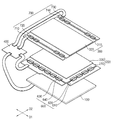
도 3은 도 1의 액정 렌즈(300)의 제1 기판(310) 및 렌즈 구동부(700)를 나타내는 평면도이다.3 is a plan view showing the
상기 제1 기판(310) 상에는 복수의 렌즈 전극들이 배치된다. 상기 렌즈 전극들은 서로 다른 폭을 가질 수 있다. 상기 렌즈 전극들은 하나의 단위 렌즈를 형성하기 위한 그룹을 형성할 수 있다. 예를 들어, 상기 그룹 내에서 가장 자리의 상기 렌즈 전극들은 상대적으로 좁은 폭을 갖고, 중심부의 상기 렌즈 전극들은 상대적으로 넓은 폭을 가질 수 있다. 이와는 달리, 상기 렌즈 전극들은 동일한 폭을 가질 수도 있다.A plurality of lens electrodes are disposed on the
상기 렌즈 전극들은 제1 방향(D1)을 따라 배치된다. 상기 렌즈 전극들은 상기 제1 방향(D1)과 교차하는 제2 방향(D2)을 따라 연장된다. 상기 렌즈 전극들은 상기 제2 방향(D2)으로부터 일정 각도로 기울어져 연장될 수 있다.The lens electrodes are arranged along the first direction D1. The lens electrodes extend along a second direction D2 that intersects the first direction D1. The lens electrodes may be inclined at an angle from the second direction D2.
상기 액정 렌즈(300)의 크기에 따라 상기 제1 렌즈 구동부 및 상기 제1 렌즈 구동부는 복수의 서브 렌즈 구동부들을 포함할 수 있다.The first lens driving unit and the first lens driving unit may include a plurality of sub lens driving units depending on the size of the
도 3에서, 상기 제1 기판(310)의 제1 변에 이웃하여 배치되는 제1 렌즈 구동부는 제1 서브 렌즈 구동부 및 제2 서브 렌즈 구동부를 포함한다. 상기 제1 기판(310)의 상기 제1 변과 마주보는 제2 변에 이웃하여 배치되는 상기 제2 렌즈 구동부는 제3 서브 렌즈 구동부 및 제4 서브 렌즈 구동부를 포함한다.3, the first lens driving unit disposed adjacent to the first side of the
제1 서브 렌즈 구동부는 제1 서브 인쇄 회로 기판(711), 제2 서브 인쇄 회로 기판(712), 제1 서브 구동 칩(721) 및 제2 서브 구동 칩(722)을 포함한다. 제2 서브 렌즈 구동부는 제3 서브 인쇄 회로 기판(731), 제2 서브 인쇄 회로 기판(732), 제3 서브 구동 칩(741) 및 제4 서브 구동 칩(742)을 포함한다.The first sub lens driver includes a first sub
상기 제1 내지 제4 서브 구동 칩(721, 722, 741, 742)들의 개수는 상기 액정 렌즈(300)의 크기에 따라 결정될 수 있다.The number of the first to fourth
상기 제1 렌즈 구동부는 상기 렌즈 전극들의 제1 단에 연결되어 렌즈 전압을 출력하고, 상기 제2 렌즈 구동부는 상기 렌즈 전극들의 제1 단에 반대되는 제2 단에 연결되어 렌즈 전압을 출력한다.The first lens driving unit is connected to the first end of the lens electrodes to output a lens voltage, and the second lens driving unit is connected to a second end opposite to the first end of the lens electrodes to output a lens voltage.
본 실시예에 따르면, 상기 렌즈 전극들은 상기 제1 렌즈 구동부 및 상기 제2 렌즈 구동부에 의해 구동되므로 상기 렌즈 전극들의 RC 응답 지연을 보상할 수 있다.According to the present embodiment, since the lens electrodes are driven by the first lens driving unit and the second lens driving unit, the RC response delay of the lens electrodes can be compensated.
도 4는 도 1의 제어부(400)를 나타내는 블록도이다.4 is a block diagram showing the
상기 제어부(400)는 영상 처리부(410), 렌즈 제어부, 패널 제어부(460), 광원 인버터(470)를 포함한다.The
상기 렌즈 제어부는 상기 서브 렌즈 구동부의 개수에 대응하는 복수의 서브 렌즈 제어부를 포함할 수 있다. 도 3에서 도시한 바와 같이 상기 렌즈 구동부가 4개의 서브 렌즈 구동부를 갖는 경우, 도 4에서 도시한 바와 같이 상기 렌즈 제어부는 제1 렌즈 제어부(420), 제2 렌즈 제어부(430), 제3 렌즈 제어부(440) 및 제4 렌즈 제어부(450)를 포함한다.The lens control unit may include a plurality of sub lens control units corresponding to the number of the sub lens driving units. As shown in FIG. 3, when the lens driving unit has four sub lens driving units, the lens control unit includes a first
상기 제어부(400)는 상기 구동 모드에 따라 상기 광원 인버터(470)의 동작을 제어하는 디밍부(480)를 더 포함할 수 있다. 상기 디밍부(480) 및 상기 광원 인버터(470)가 상기 제4 렌즈 제어부(450)에 연결되는 것을 도시하였으나, 상기 디밍부(480) 및 상기 광원 인버터(470)는 상기 제1 내지 제3 렌즈 제어부(420 내지 440) 중 어느 하나에 연결될 수 있다. 또한, 상기 디밍부(480) 및 상기 광원 인버터(470)는 복수의 상기 렌즈 제어부들에 연결될 수 있다.The
상기 영상 처리부(410)는 외부로부터 상기 입력 영상 데이터, 상기 입력 렌즈 데이터 및 상기 입력 제어 신호를 수신한다. 상기 영상 처리부(410)는 상기 입력 영상 데이터를 기초로 상기 구동 모드를 판단할 수 있다. 이와는 달리, 상기 영상 처리부(410)는 상기 구동 모드를 외부로부터 수신할 수 있다. 또한, 상기 구동 모드를 판단하는 구동 모드 판단부는 상기 영상 처리부(410)와 독립적으로 형성될 수 있다.The
상기 영상 처리부(410)는 상기 입력 제어 신호 및 상기 구동 모드를 상기 패널 제어부(600)에 출력한다.The
상기 구동 모드가 2차원 모드일 때, 상기 영상 처리부(410)는 상기 입력 영상 데이터를 상기 패널 제어부(600)에 출력한다.When the driving mode is the two-dimensional mode, the
상기 구동 모드가 3차원 모드일 때, 상기 영상 처리부(410)는 상기 입력 영상 데이터를 렌더링하여 상기 3차원 영상 데이터를 생성한다. 상기 영상 처리부(410)는 상기 3차원 영상 데이터를 상기 패널 제어부(600)에 출력한다.When the driving mode is the three-dimensional mode, the
상기 영상 처리부(410)는 상기 입력 제어 신호 및 상기 구동 모드 및 상기 입력 렌즈 데이터를 상기 제1 내지 제4 렌즈 제어부들(420 내지 450)에 출력한다.The
상기 구동 모드가 2차원 모드일 때, 상기 제1 내지 제4 렌즈 제어부들(420 내지 450)은 동작하지 않는다. 예를 들어, 상기 제1 내지 제4 렌즈 제어부들(420 내지 450)은 0V의 렌즈 데이터 신호를 상기 제1 내지 제4 서브 인쇄 회로 기판들(711, 712, 731, 732)에 출력할 수 있다.When the driving mode is the two-dimensional mode, the first through fourth
상기 구동 모드가 3차원 모드일 때, 상기 제1 내지 제4 렌즈 제어부들(420 내지 450)은 상기 입력 렌즈 데이터를 재배치하여 상기 렌즈 데이터 신호를 생성한다. 또한, 상기 입력 제어 신호를 기초로 상기 렌즈 제어 신호를 생성한다. 상기 제1 내지 제4 렌즈 제어부들(420 내지 450)은 상기 렌즈 데이터 신호 및 상기 렌즈 제어 신호를 상기 제1 내지 제4 서브 인쇄 회로 기판들(711, 712, 731, 732)에 출력한다.When the driving mode is the three-dimensional mode, the first to fourth
예를 들어, 상기 렌즈 제어 신호는 수평 개시 신호 및 로드 신호일 수 있다. 상기 수평 개시 신호는 상기 입력 영상 데이터의 상기 수직 동기 신호와 동일한 주기를 가질 수 있다. 상기 수평 개시 신호의 주기는 상기 입력 영상 데이터의 프레임 주기와 동일할 수 있다.For example, the lens control signal may be a horizontal start signal and a load signal. The horizontal start signal may have the same period as the vertical synchronous signal of the input image data. The period of the horizontal start signal may be the same as the frame period of the input image data.
상기 제1 내지 제4 렌즈 제어부들(420 내지 450)의 동작은 실질적으로 동일하다. 상기 제1 렌즈 제어부(420)의 동작에 대해 도 5를 참조하여 자세히 설명한다.The operations of the first to fourth
상기 패널 제어부(460)는 상기 구동 모드, 상기 입력 제어 신호 및 상기 입력 영상 데이터를 기초로 패널 제어 신호 및 패널 데이터 신호를 생성하여 패널 구동부(600)에 출력한다.The
상기 광원 인버터(470)는 상기 광원 제어 신호를 생성하여 상기 광원 구동부(500)에 출력한다. 상기 광원 제어 신호는 전압일 수 있다.The
상기 디밍부(480)는 상기 제4 렌즈 제어부(450) 및 상기 광원 인버터(470)에 연결된다. 상기 디밍부(480)는 상기 제4 렌즈 제어부(450)로부터 상기 구동 모드를 수신하여, 상기 광원 제어 신호의 레벨을 제어한다. 상기 디밍부(480)의 동작에 대해서는 도 10을 참조하여 자세히 설명한다.The
도 5는 도 4의 제1 렌즈 제어부(420)를 나타내는 블록도이다.5 is a block diagram showing the first
도 4 및 도 5를 참조하면, 상기 제1 렌즈 제어부(420)는 신호 생성부(421), 전원 생성부(422), 공통 전압 생성부(423) 및 데이터 처리부(424)를 포함한다.4 and 5, the first
상기 신호 생성부(421)는 상기 영상 처리부(410)로부터 상기 구동 모드 및 상기 입력 제어 신호를 수신한다. 상기 구동 모드가 3차원 모드일 때, 상기 신호 생성부(421)는 상기 렌즈 제어 신호를 생성한다. 상기 신호 생성부(421)는 상기 렌즈 제어 신호를 상기 제1 서브 렌즈 구동부에 출력한다.The
상기 전원 생성부(422)는 상기 제1 렌즈 제어부(420)에 연결된 상기 제1 서브 렌즈 구동부에서 요구되는 전원을 생성하여, 상기 제1 서브 렌즈 구동부에 출력한다.The
상기 공통 전압 생성부(423)는 상기 액정 렌즈(300)의 상기 제2 기판(320)의 공통 전극에 인가되는 공통 전압을 생성한다. 상기 공통 전압 생성부(423)는 상기 공통 전압을 상기 제2 기판(320)에 출력한다. 상기 공통 전압은 상기 제1 서브 렌즈 구동부를 거쳐 상기 제2 기판(320)에 인가될 수 있다. 상기 공통 전압 생성부(423)는 상기 제1 렌즈 제어부(420)에 배치되는 것을 도시하였으나, 상기 공통 전압 생성부(423)는 상기 제2 내지 제4 렌즈 제어부(430 내지 450) 중 어느 하나에 배치될 수 있다. 또한, 상기 공통 전압 생성부(423)는 복수의 렌즈 제어부들에 배치될 수 있다.The
상기 데이터 처리부(424)는 상기 영상 처리부(410)로부터 상기 구동 모드 및 상기 입력 렌즈 데이터를 수신한다. 상기 구동 모드가 3차원 모드일때, 상기 데이터 처리부(424)는 상기 입력 렌즈 데이터를 재배치하여 상기 렌즈 데이터 신호를 생성한다. 상기 데이터 처리부(424)는 상기 렌즈 데이터 신호를 상기 제1 서브 렌즈 구동부에 출력한다.The
도 6은 도 3의 제1 서브 구동 칩(721)을 나타내는 블록도이다.6 is a block diagram showing the first
도 6을 참조하면, 상기 제1 서브 구동 칩(721)은 상기 제1 렌즈 제어부(420)로부터 상기 렌즈 제어 신호 및 상기 렌즈 데이터 신호(DATA)를 수신한다. 상기 렌즈 제어 신호는 상기 수평 개시 신호(STH) 및 상기 로드 신호(TP)를 포함한다.Referring to FIG. 6, the first
상기 제1 서브 구동칩(721)은 쉬프트 레지스터(SR), 래치(LATCH), 신호 처리부(DAC) 및 버퍼부(BUFFER)를 포함한다. 상기 쉬프트 레지스터(SR)는 상기 수평 개시 신호(STH)를 수신하여 래치 펄스를 상기 래치에 출력한다. 상기 래치(LATCH)는 상기 렌즈 데이터 신호(DATA)를 일시 저장한다. 상기 래치(LATCH)는 상기 로드 신호(TP)에 응답하여 상기 렌즈 데이터 신호(DATA)를 출력한다. 상기 신호 처리부(DAC)는 상기 디지털 형태인 상기 렌즈 데이터 신호(DATA)를 아날로그 형태의 렌즈 전압(VD)으로 변환하여 출력한다. 상기 버퍼부(BUFFER)는 상기 신호 처리부(DAC)에서 출력되는 상기 렌즈 전압(VD)의 레벨을 보상하여 상기 렌즈 전압(VD)을 출력한다.The first
도 7은 도 5의 신호 생성부(421)에서 생성되는 렌즈 제어 신호(STH, TP) 및 도 5의 전원 생성부(422)에서 생성되는 렌즈 전원 전류(IL)를 나타내는 파형도이다.7 is a waveform diagram showing lens control signals STH and TP generated by the
도 7을 참조하면, 상기 수평 개시 신호(STH)는 프레임 단위로 온이 되는 펄스파를 갖는다. 상기 로드 신호(TP)는 복수 개의 펄스파를 갖는다. 상기 렌즈 전원 전류(IL)는 상기 렌즈 구동부로 전달되는 전원 전류를 나타낸다. 상기 렌즈 전원 전류(IL)는 상기 로드 신호(TP)의 라이징 에지에서 상기 렌즈 구동부에 순간적으로 제공되고, 시간의 흐름에 따라 점차적으로 줄어든다.Referring to FIG. 7, the horizontal start signal STH has a pulse wave which is turned on for each frame. The load signal TP has a plurality of pulse springs. The lens power supply current IL represents a power supply current supplied to the lens driver. The lens power supply current IL is momentarily provided to the lens driving unit at the rising edge of the load signal TP, and gradually decreases with the passage of time.
상기 로드 신호(TP)의 복수 개의 펄스파는 도 3의 서브 구동 칩들의 개수에 대응한다.The plurality of pulse waves of the load signal TP correspond to the number of the sub-driving chips shown in FIG.
예를 들어, 제1 렌즈 제어부(420)의 신호 생성부(421)에서 생성하는 상기 로드 신호(TP)는 한 프레임 내에서 8개의 펄스파를 가지면, 상기 제1 서브 렌즈 구동부는 제1 서브 인쇄 회로 기판(711)과 연결되는 8개의 제1 서브 구동 칩(721)을 포함한다. 상기 로드 신호(TP)의 첫번째 펄스파는 상기 제1 서브 렌즈 구동부의 첫 번째 구동 칩과 대응하고, 상기 로드 신호(TP)의 두 번째 펄스파는 상기 제1 서브 렌즈 구동부의 두 번째 구동 칩과 대응한다.For example, if the load signal TP generated by the
결과적으로, 상기 첫 번째 구동 칩에 연결되는 단위 렌즈들과 상기 두 번째 구동 칩에 연결되는 단위 렌즈들은 서로 다른 타이밍에 구동된다.As a result, the unit lenses connected to the first driving chip and the unit lenses connected to the second driving chip are driven at different timings.
본 실시예에 따르면, 상기 단위 렌즈들의 구동 타이밍을 서로 다르게 조절하여 상기 렌즈 전원 전류(IL)의 피크 값을 낮출 수 있다. 따라서, 상기 전원 생성부(422) 및 상기 렌즈 구동부가 파괴되는 것을 방지할 수 있고, 소비 전력을 감소시킬 수 있다.According to the present embodiment, the peak value of the lens power supply current IL can be lowered by controlling the driving timings of the unit lenses to be different from each other. Therefore, the
또한, 상기 제1 서브 구동 칩들(721)은 모두 1 프레임 이내에 구동되므로, 상기 액정 렌즈(300)가 정상적으로 동작할 수 있다.In addition, since all the first
도 8은 도 5의 공통 전압 생성부(423)의 동작을 나타내는 개념도이다. 도 9는 도 2의 렌즈 구동 칩(720, 740)에서 출력되는 렌즈 전압(VD) 및 도 5의 공통 전압 생성부(423)에서 생성되는 공통 전압(VCOM)을 나타내는 파형도이다.8 is a conceptual diagram showing the operation of the
도 2, 도 5, 도 8 및 도 9를 참조하면, 상기 공통 전압 생성부(423)는 상기 공통 전압(VCOM)을 생성하여 상기 액정 렌즈(300)의 상기 제2 기판(320)의 상기 공통 전극에 인가한다. 상기 렌즈 전극과 상기 공통 전극은 상대적으로 큰 커플링 캐패시턴스를 갖는다.2, 5, 8 and 9, the
그러므로, 상기 공통 전압 생성부(423)가 일정한 레벨을 갖는 공통 전압(VCOM)을 생성하면, 상기 렌즈 전극에 인가되는 상기 렌즈 전압(VD)의 라이징 에지 및 폴링 에지에서 상기 공통 전압(VCOM)의 레벨이 상기 렌즈 전압(VD)에 따라 변하게 된다.Therefore, when the
예를 들어, 상기 렌즈 전압(VD)이 로우 렌즈 전압(VDL)에서 하이 렌즈 전압(VDH)으로 증가하는 라이징 에지에서 상기 공통 전압(VCOM)의 레벨이 증가할 수 있다. 상기 렌즈 전압(VD)이 상기 하이 렌즈 전압(VDH)에서 상기 로우 렌즈 전압(VDL)으로 감소하는 폴링 에지에서 상기 공통 전압(VCOM)의 레벨이 감소할 수 있다. 따라서, 상기 액정 렌즈(300)의 기능이 악화된다.For example, the level of the common voltage VCOM may increase at a rising edge at which the lens voltage VD increases from the low lens voltage VDL to the high lens voltage VDH. The level of the common voltage VCOM may be reduced at a falling edge at which the lens voltage VD decreases from the high lens voltage VDH to the low lens voltage VDL. Therefore, the function of the
본 실시예의 상기 공통 전압 생성부(423)는 제1 전압(VC), 제2 전압(VCH) 및 제3 전압(VCL)을 갖는 공통 전압(VCOM)을 선택적으로 생성한다.The
상기 제1 전압(VC)은 정상 상태의 공통 전압이고, 상기 제2 전압(VCH)은 상기 제1 전압(VC)보다 크며, 상기 제3 전압(VCL)은 상기 제1 전압(VC)보다 작다.Wherein the first voltage VC is a steady state common voltage and the second voltage VCH is greater than the first voltage VC and the third voltage VCL is less than the first voltage VC .
상기 공통 전압 생성부(423)는 상기 렌즈 전압(VD)의 폴링 에지에서 상기 제2 전압(VCH)의 레벨을 갖는 상기 공통 전압(VCOM)을 생성한다. 상기 공통 전압 생성부(423)는 상기 렌즈 전압(VD)의 라이징 에지에서 상기 제3 전압(VCL)의 레벨을 갖는 상기 공통 전압(VCOM)을 생성한다. 상기 공통 전압 생성부(423)는 상기 라이징 에지 및 폴링 에지를 제외하면, 상기 제1 전압(VC)의 레벨을 갖는 상기 공통 전압(VCOM)을 생성한다.The
상기 제2 전압(VCH) 및 상기 제3 전압(VCL)의 레벨은 상기 입력 렌즈 데이터를 고려하여 결정할 수 있다.The level of the second voltage VCH and the level of the third voltage VCL may be determined in consideration of the input lens data.
상기 공통 전압 생성부(423)는 스위치를 포함할 수 있다. 상기 공통 전압 생성부(423)는 아날로그 멀티플렉서(Multiplexer, MUX)를 포함할 수 있다. 상기 공통 전압 생성부(423)는 카운터를 더 포함할 수 있다.The
상기 공통 전압 생성부(423)의 제어 신호(CONT)는 상기 입력 영상 데이터의 수직 동기 신호 및 반전 신호를 이용하여 생성할 수 있다. 상기 제어 신호(CONT)는 상기 카운터의 출력 신호를 이용하여 생성할 수 있다. 상기 카운터는 상기 폴링 에지로부터 상기 제2 전압(VCH)을 출력할 시간을 설정하기 위해 사용될 수 있다. 상기 카운터는 상기 라이징 에지로부터 상기 제3 전압(VCL)을 출력할 시간을 설정하기 위해 사용될 수 있다.The control signal CONT of the
본 실시예에 따르면, 상기 렌즈 전극 및 상기 공통 전극 간의 커플링 캐패시턴스에 의한 상기 공통 전압의 증가 및 감소를 보상하여, 일정한 공통 전압(VCOM)을 출력할 수 있다.According to the present embodiment, it is possible to compensate for the increase and decrease of the common voltage due to the coupling capacitance between the lens electrode and the common electrode, thereby outputting a constant common voltage VCOM.
도 10은 도 4의 디밍부(480)의 동작을 나타내는 개념도이다.10 is a conceptual diagram showing the operation of the
상기 액정 렌즈(300)는 상기 2차원 모드에서는 상기 표시 패널(200)의 영상을 그대로 통과시키고, 상기 3차원 모드에서는 표시 패널(200)의 영상을 굴절시켜 통과시킨다. 그러므로, 상기 3차원 모드에서 상기 표시 장치의 휘도는 상기 2차원 모드에 비해 낮은 값을 갖는다.The
도 4 및 도 10을 참조하면, 상기 디밍부(480)는 상기 구동 모드(MODE)에 따라 서로 다른 광원 제어 신호(DS)를 출력한다. 상기 디밍부(480)는 상기 구동 모드(MODE)가 2차원 모드일 때, 상기 2차원 디밍 신호(V2D)를 출력한다. 상기 디밍부(480)는 상기 구동 모드(MODE)가 3차원 모드일 때, 상기 3차원 디밍 신호(V3D)를 출력한다.Referring to FIGS. 4 and 10, the
상기 3차원 디밍 신호(V3D)는 상기 2차원 디밍 신호(V2D)보다 큰 값을 갖는다. 예를 들어, 상기 3차원 디밍 신호(V3D)는 상기 2차원 디밍 신호(V2D)보다 10% 큰 값을 가질 수 있다.The three-dimensional dimming signal V3D has a larger value than the two-dimensional dimming signal V2D. For example, the 3D dimming signal V3D may have a value 10% larger than the 2D dimming signal V2D.
상기 디밍부(480)에 의해 상기 광원 구동부(500)는 상기 구동 모드(MODE)에 따라 서로 다른 광원 구동 전압을 상기 광원부(100)에 인가한다. 상기 3차원 모드의 광원 구동 전압은 상기 2차원 모드의 광원 구동 전압보다 큰 값을 갖는다.The
상기 디밍부(480)는 스위치를 포함할 수 있다. 상기 디밍부(480)는 아날로그 멀티플렉서를 포함할 수 있다. 상기 디밍부(480)의 제어 신호는 상기 구동 모드(MODE)일 수 있다.The
상기 제4 렌즈 제어부(732) 및 상기 디밍부(480) 사이에는 접지 분리기가 더 형성될 수 있다. 상기 접지 분리기는 상기 제4 렌즈 제어부(732)의 접지와 상기 디밍부(480)의 접지를 분리한 상태에서 상기 구동 모드(MODE)를 상기 제4 렌즈 제어부(732)로부터 상기 디밍부(480)로 전달한다.A ground separator may be further provided between the fourth
상기 영상 처리부(410) 및 상기 제1 내지 제4 렌즈 제어부(420 내지 450)는 상대적으로 작은 전압에 의해 제어되는 반면, 상기 광원 인버터(470)는 상대적으로 큰 전압에 의해 제어되므로, 상기 접지를 서로 분리하여, 더욱 안정적으로 상기 액정 렌즈(300)를 구동할 수 있다.Since the
본 실시예에 따르면, 상기 표시 장치는 상기 디밍부(480)에 의해 상기 구동 모드에 관계 없이 균일한 휘도를 가질 수 있다.According to the present embodiment, the display device can have a uniform luminance regardless of the driving mode by the
도 11은 도 5의 공통 전압 생성부(423) 및 상기 공통 전압 생성부(423)에 연결되는 공통 전압 차단부(425)를 나타내는 블록도이다. 도 12는 도 11의 공통 전압 차단부(425)의 동작을 나타내는 개념도이다. 도 13은 도 4의 영상 처리부(410)에서 판단되는 구동 모드(MODE), 도 2의 렌즈 구동 칩(720, 740)에서 출력되는 렌즈 전압(VD) 및 도 11의 공통 전압 차단부(425)를 통과하는 공통 전압(VCOM)을 나타내는 파형도이다.11 is a block diagram showing a common
상기 구동 모드(MODE)가 3차원 모드에서 2차원 모드로 변경되면, 상기 렌즈 전극의 렌즈 전압은 상기 렌즈 구동부의 동작에 의해 즉시 0V로 떨어지는 반면, 상기 공통 전극은 서서히 0V로 떨어지므로, 상기 액정 렌즈(300)에 잔상이 남을 수 있다. 이로 인해, 상기 2차원 모드에서의 표시 품질이 악화될 수 있다.When the driving mode (MODE) is changed from the three-dimensional mode to the two-dimensional mode, the lens voltage of the lens electrode drops immediately to 0V by the operation of the lens driving unit, while the common electrode gradually falls to 0V, A residual image may remain on the
도 11 및 도 12를 참조하면, 상기 공통 전압 생성부(423)는 상기 공통 전압(VCOM)을 생성하여, 상기 액정 렌즈(300)의 상기 제2 기판(320)의 공통 전극에 인가한다. 상기 공통 전압 차단부(425)는 상기 구동 모드(MODE)에 따라 상기 공통 전압을 선택적으로 출력할 수 있다.Referring to FIGS. 11 and 12, the
상기 3차원 모드에서 상기 공통 전압 차단부(425)는 상기 공통 전압 생성부(423)에서 생성한 상기 공통 전압(VCOM)을 그대로 통과시킨다.In the three-dimensional mode, the
상기 2차원 모드에서 상기 공통 전압 차단부(425)는 상기 공통 전압(VCOM)을 0V로 설정한다.In the two-dimensional mode, the
상기 공통 전압 차단부(425)는 스위치를 포함할 수 있다. 상기 공통 전압 차단부(425)는 파워 MOSFET을 포함할 수 있다. 상기 공통 전압 차단부(425)의 제어 신호는 상기 구동 모드(MODE)일 수 있다.The
도 13을 참조하면, 상기 구동 모드(MODE)가 상기 3차원 모드(3D)에서 상기 2차원 모드(2D)로 변화하는 즉시, 하이 렌즈 전압(VDH) 및 로우 렌즈 전압(VDL) 사이에서 증가 및 감소하고 있는 상기 렌즈 전압(VD)은 0V로 감소한다.13, as soon as the driving mode MODE changes from the three-
상기 구동 모드(MODE)가 상기 3차원 모드(3D)에서 상기 2차원 모드(2D)로 변화하는 즉시, 상기 공통 전압(VOCM)은 0V로 감소한다.As soon as the drive mode (MODE) changes from the three-dimensional mode (3D) to the two-dimensional mode (2D), the common voltage (VOCM) decreases to 0V.
본 실시예에 따르면, 상기 구동 모드(MODE)가 상기 3차원 모드에서 상기 2차원 모드로 변할 때, 상기 공통 전압(VCOM)을 0V로 즉시 설정하므로, 상기 액정 렌즈(300)의 잔상을 제거하여 표시 품질을 향상시킬 수 있다.According to this embodiment, when the driving mode (MODE) is changed from the three-dimensional mode to the two-dimensional mode, the common voltage VCOM is immediately set to 0 V, so that the residual image of the
이상에서 설명한 본 발명에 따른 액정 렌즈의 구동 방법, 액정 렌즈 모듈 및 표시 장치에 따르면, 렌즈 전극들은 제1 렌즈 구동부 및 제2 렌즈 구동부에 의해 구동되므로 상기 렌즈 전극들의 RC 응답 지연을 보상할 수 있다.According to the driving method of the liquid crystal lens, the liquid crystal lens module and the display device according to the present invention, since the lens electrodes are driven by the first lens driving unit and the second lens driving unit, the RC response delay of the lens electrodes can be compensated .
또한, 단위 렌즈들의 구동 타이밍을 서로 다르게 조절하여 전원 생성부 및 렌즈 구동부가 파괴되는 것을 방지할 수 있고, 소비 전력을 감소시킬 수 있다.In addition, it is possible to prevent the power generating unit and the lens driving unit from being broken by adjusting the driving timings of the unit lenses to different from each other, and to reduce the power consumption.
또한, 상기 렌즈 전극 및 공통 전극 간의 커플링 캐패시턴스에 의한 공통 전압의 증가 및 감소를 보상하여, 일정한 공통 전압(VCOM)을 출력할 수 있다.In addition, it is possible to compensate for the increase and decrease of the common voltage due to the coupling capacitance between the lens electrode and the common electrode, thereby outputting a constant common voltage VCOM.
또한, 디밍부에 의해 표시 장치는 구동 모드에 관계 없이 균일한 휘도를 가질 수 있다.Further, the display device can have a uniform luminance regardless of the driving mode by the dimming section.
또한, 3차원 모드에서 상기 2차원 모드로 변할 때 상기 액정 렌즈의 잔상을 제거하여 표시 품질을 향상시킬 수 있다.Also, when the three-dimensional mode is changed to the two-dimensional mode, the afterimage of the liquid crystal lens can be removed to improve the display quality.
이상에서는 본 발명의 바람직한 실시예들을 참조하여 설명하였지만, 해당 기술분야의 숙련된 당업자 또는 해당 기술분야에 통상의 지식을 갖는 자라면 후술될 특허청구범위에 기재된 본 발명의 사상 및 기술 영역으로부터 벗어나지 않는 범위 내에서 본 발명을 다양하게 수정 및 변경시킬 수 있음을 이해할 수 있을 것이다.While the present invention has been described with reference to exemplary embodiments, it is to be understood that the invention is not limited to the disclosed exemplary embodiments, but, on the contrary, is intended to cover various modifications and equivalent arrangements included within the spirit and scope of the appended claims. It will be understood that various modifications and changes may be made thereto without departing from the scope of the present invention.
100: 광원부 200: 표시 패널
300: 액정 렌즈 400: 제어부
410: 영상 처리부 420: 제1 렌즈 제어부
430: 제2 렌즈 제어부 440: 제3 렌즈 제어부
450: 제4 렌즈 제어부 460: 패널 제어부
470: 광원 인버터 480: 디밍부
500: 광원 구동부 600: 패널 구동부
700: 렌즈 구동부100: light source 200: display panel
300: liquid crystal lens 400:
410: image processor 420: first lens controller
430: Second lens control unit 440: Third lens control unit
450: fourth lens control unit 460:
470: Light source inverter 480: Dimming unit
500: light source driver 600: panel driver
700:
Claims (20)
상기 3차원 모드에서 서로 다른 타이밍을 갖는 펄스들을 갖는 렌즈 제어 신호들을 수신하여 복수의 단위 렌즈들을 포함하는 액정 렌즈의 상기 단위 렌즈들을 상기 렌즈 제어 신호들의 펄스들을 기초로 서로 다른 타이밍으로 구동하는 단계를 포함하는 액정 렌즈의 구동 방법.Determining a drive mode including a two-dimensional mode and a three-dimensional mode; And
Receiving the lens control signals having pulses having different timings in the three-dimensional mode and driving the unit lenses of the liquid crystal lens including a plurality of unit lenses at different timings based on the pulses of the lens control signals And a driving method of the liquid crystal lens.
상기 서로 다른 타이밍을 갖는 펄스들을 갖는 상기 렌즈 제어 신호들을 생성하는 단계; 및
상기 렌즈 제어 신호들을 복수의 렌즈 전극들과 연결되는 각각의 렌즈 구동 칩들에 출력하는 단계를 포함하는 것을 특징으로 하는 액정 렌즈의 구동 방법.2. The method of claim 1, wherein driving the unit lenses comprises:
Generating the lens control signals having pulses with different timings; And
And outputting the lens control signals to the respective lens driving chips connected to the plurality of lens electrodes.
렌즈 전극의 제1 단에 렌즈 전압을 출력하고, 상기 렌즈 전극의 상기 제1 단에 반대되는 제2 단에 렌즈 전압을 출력하는 것을 특징으로 하는 액정 렌즈의 구동 방법.2. The method of claim 1, wherein driving the unit lenses comprises:
Wherein a lens voltage is outputted to a first end of the lens electrode and a lens voltage is outputted to a second end opposite to the first end of the lens electrode.
상기 공통 전압을 생성하는 단계는 제1 전압, 제2 전압 및 제3 전압을 선택하는 것을 특징으로 하는 액정 렌즈의 구동 방법.2. The method of claim 1, wherein driving the unit lenses further comprises generating a common voltage and outputting the common voltage to a common electrode,
Wherein the step of generating the common voltage comprises selecting a first voltage, a second voltage and a third voltage.
입력 영상 데이터의 수직 동기 신호 및 반전 신호를 이용하여 상기 제1, 제2 및 제3 전압들을 선택하는 것을 특징으로 하는 액정 렌즈의 구동 방법.5. The method of claim 4, wherein generating the common voltage comprises:
Wherein the first, second, and third voltages are selected using a vertical synchronizing signal and an inverting signal of the input image data.
상기 제2 전압은 렌즈 전극에 인가되는 렌즈 전압의 폴링 에지에서 출력되고, 상기 제3 전압은 상기 렌즈 전압의 라이징 에지에서 출력되는 것을 특징으로 하는 액정 렌즈의 구동 방법.6. The method of claim 5, wherein the first voltage is a steady state common voltage, the second voltage is greater than the first voltage, the third voltage is less than the first voltage,
Wherein the second voltage is output at a falling edge of a lens voltage applied to the lens electrode, and the third voltage is outputted at a rising edge of the lens voltage.
상기 2차원 모드의 광원 구동 전압보다 큰 것을 특징으로 하는 액정 렌즈의 구동 방법.8. The method of claim 7, wherein the light source driving voltage in the three-
Dimensional mode is larger than the light source driving voltage of the two-dimensional mode.
상기 2차원 모드에서 상기 공통 전압을 0V로 설정하는 것을 특징으로 하는 액정 렌즈의 구동 방법.2. The method of claim 1, wherein driving the unit lenses further comprises generating a common voltage and outputting the common voltage to a common electrode,
And the common voltage is set to 0 V in the two-dimensional mode.
Priority Applications (2)
| Application Number | Priority Date | Filing Date | Title |
|---|---|---|---|
| KR1020110030267A KR101811642B1 (en) | 2011-04-01 | 2011-04-01 | Method of driving liquid crystal lens, liquid crystal module for performing the same and display apparatus having the same |
| US13/242,823 US9341871B2 (en) | 2011-04-01 | 2011-09-23 | Method of driving liquid crystal lens, liquid crystal lens module for performing the method and display apparatus having the liquid crystal lens module |
Applications Claiming Priority (1)
| Application Number | Priority Date | Filing Date | Title |
|---|---|---|---|
| KR1020110030267A KR101811642B1 (en) | 2011-04-01 | 2011-04-01 | Method of driving liquid crystal lens, liquid crystal module for performing the same and display apparatus having the same |
Publications (2)
| Publication Number | Publication Date |
|---|---|
| KR20120111649A KR20120111649A (en) | 2012-10-10 |
| KR101811642B1 true KR101811642B1 (en) | 2017-12-27 |
Family
ID=46926565
Family Applications (1)
| Application Number | Title | Priority Date | Filing Date |
|---|---|---|---|
| KR1020110030267A Expired - Fee Related KR101811642B1 (en) | 2011-04-01 | 2011-04-01 | Method of driving liquid crystal lens, liquid crystal module for performing the same and display apparatus having the same |
Country Status (2)
| Country | Link |
|---|---|
| US (1) | US9341871B2 (en) |
| KR (1) | KR101811642B1 (en) |
Families Citing this family (8)
| Publication number | Priority date | Publication date | Assignee | Title |
|---|---|---|---|---|
| TWI446326B (en) * | 2011-08-22 | 2014-07-21 | Chunghwa Picture Tubes Ltd | Control circuit for generating a backlight driving current and method thereof |
| KR102134904B1 (en) | 2013-10-30 | 2020-07-17 | 삼성디스플레이 주식회사 | Three dimensional image display and liquid crystal lens therefor |
| KR102164958B1 (en) * | 2013-11-11 | 2020-10-14 | 삼성디스플레이 주식회사 | Three-dimensional image display apparatus |
| KR20150066363A (en) | 2013-12-06 | 2015-06-16 | 삼성디스플레이 주식회사 | Liquid crystal lens module |
| KR102230549B1 (en) | 2014-09-12 | 2021-03-22 | 삼성디스플레이 주식회사 | Touch sensible optical system and display device including the same |
| CN105278181B (en) * | 2015-11-05 | 2018-09-11 | 武汉华星光电技术有限公司 | Response time short liquid crystal display panel and display device |
| US10530186B2 (en) * | 2017-08-10 | 2020-01-07 | Texas Instruments Incorporated | Wireless power transmission with fractional timing resolution |
| CN110572493A (en) * | 2019-09-08 | 2019-12-13 | 深圳奇屏科技有限公司 | Double-screen mobile phone with naked eye 3D display screen |
Citations (1)
| Publication number | Priority date | Publication date | Assignee | Title |
|---|---|---|---|---|
| US20110063533A1 (en) * | 2009-09-17 | 2011-03-17 | Hwi Kim | Method of displaying stereoscopic images mixed with monoscopic images and mono/stereoscopic image display apparatus capable of performing the method |
Family Cites Families (10)
| Publication number | Priority date | Publication date | Assignee | Title |
|---|---|---|---|---|
| KR100293983B1 (en) | 1997-12-26 | 2001-10-26 | 윤종용 | Dot inversion driving device and method in dual bank structure of liquid crystal display |
| JP2000102038A (en) | 1998-09-18 | 2000-04-07 | Sanyo Electric Co Ltd | Two-dimensional video image and three-dimensional video image compatible type video display device |
| KR101521660B1 (en) | 2008-12-24 | 2015-05-20 | 엘지디스플레이 주식회사 | Liquid crystal lens device |
| JP5185145B2 (en) | 2009-01-16 | 2013-04-17 | 株式会社東芝 | Stereoscopic image display apparatus and stereoscopic image display method |
| KR20110014311A (en) * | 2009-08-05 | 2011-02-11 | 삼성전자주식회사 | Liquid crystal lens panel, manufacturing method thereof and display device having same |
| JP2011095369A (en) * | 2009-10-28 | 2011-05-12 | Sony Corp | Stereoscopic image display device and method of driving the same |
| CN102116936B (en) * | 2009-12-30 | 2013-12-11 | 鸿富锦精密工业(深圳)有限公司 | Stereopicture display |
| US8427626B2 (en) * | 2010-01-27 | 2013-04-23 | Sony Corporation | Lens array element and image display device |
| KR101324412B1 (en) * | 2010-05-06 | 2013-11-01 | 엘지디스플레이 주식회사 | Stereoscopic image display and driving method thereof |
| US20120235991A1 (en) * | 2011-03-15 | 2012-09-20 | Industrial Technology Research Institute | Three dimensional display and driving method thereof |
-
2011
- 2011-04-01 KR KR1020110030267A patent/KR101811642B1/en not_active Expired - Fee Related
- 2011-09-23 US US13/242,823 patent/US9341871B2/en not_active Expired - Fee Related
Patent Citations (1)
| Publication number | Priority date | Publication date | Assignee | Title |
|---|---|---|---|---|
| US20110063533A1 (en) * | 2009-09-17 | 2011-03-17 | Hwi Kim | Method of displaying stereoscopic images mixed with monoscopic images and mono/stereoscopic image display apparatus capable of performing the method |
Also Published As
| Publication number | Publication date |
|---|---|
| KR20120111649A (en) | 2012-10-10 |
| US9341871B2 (en) | 2016-05-17 |
| US20120249506A1 (en) | 2012-10-04 |
Similar Documents
| Publication | Publication Date | Title |
|---|---|---|
| KR101811642B1 (en) | Method of driving liquid crystal lens, liquid crystal module for performing the same and display apparatus having the same | |
| KR101324412B1 (en) | Stereoscopic image display and driving method thereof | |
| CN102378018B (en) | Stereoscopic image display and method for driving the same | |
| KR101279128B1 (en) | Stereoscopic image display and driving method thereof | |
| US8294753B2 (en) | Image display device and method of driving the same | |
| US8982196B2 (en) | Three-dimensional image display device | |
| US9001197B2 (en) | Stereoscopic image display device | |
| US9030450B2 (en) | Display apparatus and method of displaying three-dimensional image using the same | |
| KR20110123076A (en) | Stereoscopic Display and Driving Method | |
| US20120274748A1 (en) | Stereoscopic Image Display Device and Method for Driving the Same | |
| US20130076737A1 (en) | Apparatus and method for displaying 3d image | |
| CN104079911B (en) | Stereoscopic display device and driving method thereof | |
| KR101923150B1 (en) | Display apparatus and method of displaying three dimensional image using the same | |
| CN103118266B (en) | Stereoscopic image display | |
| US20130147863A1 (en) | Method of displaying three-dimensional stereoscopic image and display apparatus for performing the same | |
| KR101688534B1 (en) | Three-dimensional display and driving method thereof | |
| US9236023B2 (en) | Liquid crystal display device, driving method, and display apparatus | |
| KR102056672B1 (en) | Stereoscopic display device | |
| KR101829461B1 (en) | Stereoscopic image display device and method for driving thereof | |
| KR20120076209A (en) | Stereoscopic image display and method of controling pixel discharging time thereof | |
| KR101859968B1 (en) | Stereoscopic image display device and method for driving thereof | |
| KR101803564B1 (en) | Stereoscopic image display device and driving method thereof | |
| KR20120047749A (en) | Stereoscopic image display device and driving method thereof | |
| KR20130035001A (en) | Stereoscopic image display and method for driving the same | |
| KR20120066575A (en) | Streoscopic image display device |
Legal Events
| Date | Code | Title | Description |
|---|---|---|---|
| PA0109 | Patent application |
St.27 status event code: A-0-1-A10-A12-nap-PA0109 |
|
| R18-X000 | Changes to party contact information recorded |
St.27 status event code: A-3-3-R10-R18-oth-X000 |
|
| N231 | Notification of change of applicant | ||
| PN2301 | Change of applicant |
St.27 status event code: A-3-3-R10-R13-asn-PN2301 St.27 status event code: A-3-3-R10-R11-asn-PN2301 |
|
| PG1501 | Laying open of application |
St.27 status event code: A-1-1-Q10-Q12-nap-PG1501 |
|
| R18-X000 | Changes to party contact information recorded |
St.27 status event code: A-3-3-R10-R18-oth-X000 |
|
| A201 | Request for examination | ||
| E13-X000 | Pre-grant limitation requested |
St.27 status event code: A-2-3-E10-E13-lim-X000 |
|
| P11-X000 | Amendment of application requested |
St.27 status event code: A-2-2-P10-P11-nap-X000 |
|
| P13-X000 | Application amended |
St.27 status event code: A-2-2-P10-P13-nap-X000 |
|
| PA0201 | Request for examination |
St.27 status event code: A-1-2-D10-D11-exm-PA0201 |
|
| E902 | Notification of reason for refusal | ||
| PE0902 | Notice of grounds for rejection |
St.27 status event code: A-1-2-D10-D21-exm-PE0902 |
|
| P11-X000 | Amendment of application requested |
St.27 status event code: A-2-2-P10-P11-nap-X000 |
|
| P13-X000 | Application amended |
St.27 status event code: A-2-2-P10-P13-nap-X000 |
|
| E701 | Decision to grant or registration of patent right | ||
| PE0701 | Decision of registration |
St.27 status event code: A-1-2-D10-D22-exm-PE0701 |
|
| GRNT | Written decision to grant | ||
| PR0701 | Registration of establishment |
St.27 status event code: A-2-4-F10-F11-exm-PR0701 |
|
| PR1002 | Payment of registration fee |
St.27 status event code: A-2-2-U10-U11-oth-PR1002 Fee payment year number: 1 |
|
| PG1601 | Publication of registration |
St.27 status event code: A-4-4-Q10-Q13-nap-PG1601 |
|
| P22-X000 | Classification modified |
St.27 status event code: A-4-4-P10-P22-nap-X000 |
|
| R18-X000 | Changes to party contact information recorded |
St.27 status event code: A-5-5-R10-R18-oth-X000 |
|
| P22-X000 | Classification modified |
St.27 status event code: A-4-4-P10-P22-nap-X000 |
|
| PR1001 | Payment of annual fee |
St.27 status event code: A-4-4-U10-U11-oth-PR1001 Fee payment year number: 4 |
|
| PR1001 | Payment of annual fee |
St.27 status event code: A-4-4-U10-U11-oth-PR1001 Fee payment year number: 5 |
|
| PR1001 | Payment of annual fee |
St.27 status event code: A-4-4-U10-U11-oth-PR1001 Fee payment year number: 6 |
|
| PC1903 | Unpaid annual fee |
St.27 status event code: A-4-4-U10-U13-oth-PC1903 Not in force date: 20231219 Payment event data comment text: Termination Category : DEFAULT_OF_REGISTRATION_FEE |
|
| PC1903 | Unpaid annual fee |
St.27 status event code: N-4-6-H10-H13-oth-PC1903 Ip right cessation event data comment text: Termination Category : DEFAULT_OF_REGISTRATION_FEE Not in force date: 20231219 |