KR101803790B1 - Thinning method and apparatus of wafer - Google Patents
Thinning method and apparatus of wafer Download PDFInfo
- Publication number
- KR101803790B1 KR101803790B1 KR1020130043080A KR20130043080A KR101803790B1 KR 101803790 B1 KR101803790 B1 KR 101803790B1 KR 1020130043080 A KR1020130043080 A KR 1020130043080A KR 20130043080 A KR20130043080 A KR 20130043080A KR 101803790 B1 KR101803790 B1 KR 101803790B1
- Authority
- KR
- South Korea
- Prior art keywords
- wafer
- line beam
- line
- interface
- laser
- Prior art date
- Legal status (The legal status is an assumption and is not a legal conclusion. Google has not performed a legal analysis and makes no representation as to the accuracy of the status listed.)
- Active
Links
Images


Classifications
-
- H10P52/00—
-
- B—PERFORMING OPERATIONS; TRANSPORTING
- B23—MACHINE TOOLS; METAL-WORKING NOT OTHERWISE PROVIDED FOR
- B23K—SOLDERING OR UNSOLDERING; WELDING; CLADDING OR PLATING BY SOLDERING OR WELDING; CUTTING BY APPLYING HEAT LOCALLY, e.g. FLAME CUTTING; WORKING BY LASER BEAM
- B23K26/00—Working by laser beam, e.g. welding, cutting or boring
- B23K26/02—Positioning or observing the workpiece, e.g. with respect to the point of impact; Aligning, aiming or focusing the laser beam
- B23K26/06—Shaping the laser beam, e.g. by masks or multi-focusing
- B23K26/073—Shaping the laser spot
- B23K26/0738—Shaping the laser spot into a linear shape
-
- B—PERFORMING OPERATIONS; TRANSPORTING
- B23—MACHINE TOOLS; METAL-WORKING NOT OTHERWISE PROVIDED FOR
- B23K—SOLDERING OR UNSOLDERING; WELDING; CLADDING OR PLATING BY SOLDERING OR WELDING; CUTTING BY APPLYING HEAT LOCALLY, e.g. FLAME CUTTING; WORKING BY LASER BEAM
- B23K26/00—Working by laser beam, e.g. welding, cutting or boring
- B23K26/08—Devices involving relative movement between laser beam and workpiece
- B23K26/083—Devices involving movement of the workpiece in at least one axial direction
- B23K26/0853—Devices involving movement of the workpiece in at least in two axial directions, e.g. in a plane
-
- B—PERFORMING OPERATIONS; TRANSPORTING
- B23—MACHINE TOOLS; METAL-WORKING NOT OTHERWISE PROVIDED FOR
- B23K—SOLDERING OR UNSOLDERING; WELDING; CLADDING OR PLATING BY SOLDERING OR WELDING; CUTTING BY APPLYING HEAT LOCALLY, e.g. FLAME CUTTING; WORKING BY LASER BEAM
- B23K26/00—Working by laser beam, e.g. welding, cutting or boring
- B23K26/08—Devices involving relative movement between laser beam and workpiece
- B23K26/0869—Devices involving movement of the laser head in at least one axial direction
- B23K26/0876—Devices involving movement of the laser head in at least one axial direction in at least two axial directions
-
- B—PERFORMING OPERATIONS; TRANSPORTING
- B23—MACHINE TOOLS; METAL-WORKING NOT OTHERWISE PROVIDED FOR
- B23K—SOLDERING OR UNSOLDERING; WELDING; CLADDING OR PLATING BY SOLDERING OR WELDING; CUTTING BY APPLYING HEAT LOCALLY, e.g. FLAME CUTTING; WORKING BY LASER BEAM
- B23K26/00—Working by laser beam, e.g. welding, cutting or boring
- B23K26/36—Removing material
- B23K26/40—Removing material taking account of the properties of the material involved
- B23K26/402—Removing material taking account of the properties of the material involved involving non-metallic material, e.g. isolators
-
- B—PERFORMING OPERATIONS; TRANSPORTING
- B23—MACHINE TOOLS; METAL-WORKING NOT OTHERWISE PROVIDED FOR
- B23K—SOLDERING OR UNSOLDERING; WELDING; CLADDING OR PLATING BY SOLDERING OR WELDING; CUTTING BY APPLYING HEAT LOCALLY, e.g. FLAME CUTTING; WORKING BY LASER BEAM
- B23K26/00—Working by laser beam, e.g. welding, cutting or boring
- B23K26/50—Working by transmitting the laser beam through or within the workpiece
- B23K26/53—Working by transmitting the laser beam through or within the workpiece for modifying or reforming the material inside the workpiece, e.g. for producing break initiation cracks
-
- B—PERFORMING OPERATIONS; TRANSPORTING
- B23—MACHINE TOOLS; METAL-WORKING NOT OTHERWISE PROVIDED FOR
- B23K—SOLDERING OR UNSOLDERING; WELDING; CLADDING OR PLATING BY SOLDERING OR WELDING; CUTTING BY APPLYING HEAT LOCALLY, e.g. FLAME CUTTING; WORKING BY LASER BEAM
- B23K26/00—Working by laser beam, e.g. welding, cutting or boring
- B23K26/70—Auxiliary operations or equipment
- B23K26/702—Auxiliary equipment
-
- B—PERFORMING OPERATIONS; TRANSPORTING
- B28—WORKING CEMENT, CLAY, OR STONE
- B28D—WORKING STONE OR STONE-LIKE MATERIALS
- B28D5/00—Fine working of gems, jewels, crystals, e.g. of semiconductor material; apparatus or devices therefor
- B28D5/0005—Fine working of gems, jewels, crystals, e.g. of semiconductor material; apparatus or devices therefor by breaking, e.g. dicing
- B28D5/0011—Fine working of gems, jewels, crystals, e.g. of semiconductor material; apparatus or devices therefor by breaking, e.g. dicing with preliminary treatment, e.g. weakening by scoring
-
- H10P50/242—
-
- H10P52/402—
-
- H10P54/00—
-
- H10W20/095—
-
- H10W20/096—
-
- H10W72/015—
-
- B—PERFORMING OPERATIONS; TRANSPORTING
- B23—MACHINE TOOLS; METAL-WORKING NOT OTHERWISE PROVIDED FOR
- B23K—SOLDERING OR UNSOLDERING; WELDING; CLADDING OR PLATING BY SOLDERING OR WELDING; CUTTING BY APPLYING HEAT LOCALLY, e.g. FLAME CUTTING; WORKING BY LASER BEAM
- B23K2101/00—Articles made by soldering, welding or cutting
- B23K2101/36—Electric or electronic devices
- B23K2101/40—Semiconductor devices
-
- B—PERFORMING OPERATIONS; TRANSPORTING
- B23—MACHINE TOOLS; METAL-WORKING NOT OTHERWISE PROVIDED FOR
- B23K—SOLDERING OR UNSOLDERING; WELDING; CLADDING OR PLATING BY SOLDERING OR WELDING; CUTTING BY APPLYING HEAT LOCALLY, e.g. FLAME CUTTING; WORKING BY LASER BEAM
- B23K2103/00—Materials to be soldered, welded or cut
- B23K2103/16—Composite materials, e.g. fibre reinforced
- B23K2103/166—Multilayered materials
- B23K2103/172—Multilayered materials wherein at least one of the layers is non-metallic
-
- B—PERFORMING OPERATIONS; TRANSPORTING
- B23—MACHINE TOOLS; METAL-WORKING NOT OTHERWISE PROVIDED FOR
- B23K—SOLDERING OR UNSOLDERING; WELDING; CLADDING OR PLATING BY SOLDERING OR WELDING; CUTTING BY APPLYING HEAT LOCALLY, e.g. FLAME CUTTING; WORKING BY LASER BEAM
- B23K2103/00—Materials to be soldered, welded or cut
- B23K2103/50—Inorganic material, e.g. metals, not provided for in B23K2103/02 – B23K2103/26
- B23K2103/56—Inorganic material, e.g. metals, not provided for in B23K2103/02 – B23K2103/26 semiconducting
Landscapes
- Engineering & Computer Science (AREA)
- Physics & Mathematics (AREA)
- Optics & Photonics (AREA)
- Mechanical Engineering (AREA)
- Plasma & Fusion (AREA)
- Oil, Petroleum & Natural Gas (AREA)
- Chemical Kinetics & Catalysis (AREA)
- General Chemical & Material Sciences (AREA)
- Chemical & Material Sciences (AREA)
- Mechanical Treatment Of Semiconductor (AREA)
- Laser Beam Processing (AREA)
- Manufacturing & Machinery (AREA)
- Condensed Matter Physics & Semiconductors (AREA)
- General Physics & Mathematics (AREA)
- Computer Hardware Design (AREA)
- Microelectronics & Electronic Packaging (AREA)
- Power Engineering (AREA)
- Dicing (AREA)
- Container, Conveyance, Adherence, Positioning, Of Wafer (AREA)
Abstract
웨이퍼의 시닝 방법 및 장치가 제공된다. 본 발명의 일 실시예에 따른 웨이퍼의 시닝 방법은, 웨이퍼의 특정 깊이에 초점이 맞추어진 라인빔을 조사하는 단계; 상기 라인빔을 이용하여 상기 웨이퍼를 스캔하여 상기 웨이퍼의 특정 깊이에 계면을 형성하는 단계; 및 상기 계면이 형성된 웨이퍼를 패턴 웨이퍼(pattern wafer)와 더미 웨이퍼(dummy wafer)로 클리빙(cleaving)하는 단계를 포함하며, 상기 계면을 형성하는 단계는, 상기 라인빔의 스캔 속도 또는 상기 라인빔의 세기 중 적어도 하나를 조정하는 단계 및 상기 웨이퍼의 특정 깊이에 격자 모양의 라인을 형성하는 단계를 포함하되, 상기 격자 모양 라인은, 상기 웨이퍼의 다이싱 공정을 대체하기 위해 기 설정된 간격으로 형성한다.A method and apparatus for thinning a wafer are provided. A method of thinning a wafer according to an embodiment of the present invention includes: irradiating a line beam focused on a specific depth of a wafer; Scanning the wafer using the line beam to form an interface at a specific depth of the wafer; And a step of cleaving the interface-formed wafer with a pattern wafer and a dummy wafer, wherein the step of forming the interface includes: And forming a lattice-like line at a specific depth of the wafer, wherein the lattice-like lines are formed at predetermined intervals to replace the dicing process of the wafer .
Description
본 발명은 웨이퍼의 시닝 방법 및 장치에 대한 것으로, 더욱 상세하게는 웨이퍼(Wafer)의 원하는 두께에 따라 특정 깊이에 초점이 맞춰진 레이저 라인 빔(Laser Line beam)을 스캔(Scan)하여 계면을 형성하여, 웨이퍼를 클리빙(Cleaving)하여 간단하게 원하는 두께로 웨이퍼를 떼어내는 웨이퍼의 시닝 방법 및 장치에 대한 것이다.The present invention relates to a method and an apparatus for thinning a wafer, and more particularly to a method and apparatus for thinning a wafer by scanning a laser line beam focused at a specific depth according to a desired thickness of a wafer, The present invention relates to a wafer thinning method and apparatus for simply removing a wafer to a desired thickness by cleaving the wafer.
전기전자 장비의 소형화 및 슬림화는 보다 얇은 다이들을 필요로 한다. 집적 회로와 같은 반도체 칩 제조시, 회로가 반도체 웨이퍼(Wafer) 상에 형성되고 그 후 각각의 부분 또는 다이로 분리되거나 개별화된다. 이것은 장치를 개별적으로 형성하는 것에 비하여 비용을 절감하고 처리를 간소하게 한다.Miniaturization and slimming of electrical and electronic equipment require thinner dies. In the manufacture of semiconductor chips such as integrated circuits, circuits are formed on semiconductor wafers and then separated or individualized into respective portions or dies. This saves costs and simplifies processing compared to forming the devices individually.
도 1은 종래의 웨이퍼로부터 다이를 분리하는 공정을 도시한 도면이다.1 is a view showing a step of separating a die from a conventional wafer.
도 1을 참조하면, 웨이퍼(1)의 일면에 형성된 회로(2)를 보호하기 위해, 보호 필름(5)이 회로(2)가 형성된 웨이퍼(1) 위에 부착된다((a) 참조). 웨이퍼(1)는 다이(3)로 분리되기 전에, 화학적 또는 기계적 평탄화, 또는 다른 재료 제거 기술들을 통하여 후면 연삭(back grinding)되는 것이 통상적이며, 이 경우 재료는 웨이퍼 하부 또는 후면으로부터 제거되어, 매끄러운 하면을 남긴다. 이러한 공정을 Wafer Back Grinding이라 한다. 즉, 반도체 조립 전에 웨이퍼(1)를 웨이퍼 척(15)으로 지지하고, 웨이퍼(1)를 그라인더(10)로 박형화하여 웨이퍼(1)의 두께를 균일하게 바로 잡음과 동시에 원하는 두께로 갈아내는 공정이다((b) 참조). 그리고, 보호 필름(5)을 제거하고, 분리 단계동안 다이를 기계적으로 지지하기 위하여, 마운트 필름(20)을 부착하고, 웨이퍼 링(25)으로 고정한다((c) 참조). 웨이퍼(1)의 상부면으로부터 웨이퍼(1)를 통하여 스크라이브 라인(30)의 기계적 생성에 의하여, 웨이퍼(1)에서 물리적으로 분리된 낱개 다이(2)로 절단된다((d) 참조). 그리고, 낱개 다이(2)를 웨이퍼(1)로부터 떼어낼 수 있도록 웨이퍼 링(25)을 이동시켜 마운트 필름(20)을 확장시킨다((e) 참조). 그리고, 웨이퍼(1)로부터 낱개 다이(2)를 완전히 분리하고((f) 참조), 분리된 다이(3)를 분리하여 집적 회로 칩내로 조립되거나, 또는 인쇄 회로 기판(PCB)에 직접 고정될 수 있으며, 다이 상에 있는 하나 이상의 전기적으로 도통하는 본딩 와이어로 전기적 접속이 이루어진다. 특히, 웨이퍼(1)에서 다이(3)를 분리하는 공정을 소잉(Sawing) 또는 다이싱(Dicing)이라 한다.1, in order to protect the
도 2는 종래의 웨이퍼 후면 연삭(Wafer Back Grinding)을 도시한 도면이며, 도 3은 종래의 웨이퍼 후면 연삭에 따른 웨이퍼의 두께 변동을 도시한 도면이다.FIG. 2 is a view showing a conventional wafer back grinding, and FIG. 3 is a view showing variation in thickness of a wafer according to a conventional wafer back grinding.
도 2 및 도 3을 참조하면, 종래의 그라인딩 휠(Grinding Wheel, 10)을 이용한 웨이퍼 연삭 기술은 고속으로 회전하는 그라인딩 휠(10)로 직접 웨이퍼(1) 면을 갈아내는 공법으로 기계적인 마찰열과 이물 제거를 위해 공정 중에 DI Water를 계속 뿌리면서 진행된다. 웨이퍼 척(Wafer Chuck, 15)위에 올려진 웨이퍼(1)는 연삭 동안에 기계적인 스트레스를 받을 수 밖에 없다. 이러한 스트레스는 그라인딩(Grinding) 후, 반대 면에 부착된 보호 필름(5)을 떼어내는 과정에서 웨이퍼(1)의 깨짐 등으로 나타나기도 한다. 웨이퍼 그라인딩(Wafer Grinding) 공정 중에 연마되지 않는, 회로(2)가 형성된 면은 보호 필름(5)이 부착된 상태로 웨이퍼 척(15)에 고정이 된다. 보호 필름(5)은 웨이퍼(1)의 회로(2) 패턴의 높낮이에 따라 굴곡을 갖게 되고 이 상태로 웨이퍼 척(15)에 고정이 된다. 웨이퍼(1)의 보호 필름(5)에 전사된 패턴 면 형상은 웨이퍼(1)가 웨이퍼 척(15)에 고정되어 연마되어 얇아 지면서 연마 면에 나타나게 되어 웨이퍼(1) 전체 두께의 변동 요인이 된다. 2 and 3, a wafer grinding technique using a
또한, 화학적으로 웨이퍼 후면을 갈아내는 에칭(Etching) 방식은 웨이퍼 면을 강한 화학약품으로 녹여서 두께를 얇게 만드는 공법이다. 이러한 방법은 약품과 웨이퍼 재질간의 화학반응을 통해 제거하는 것으로, 기계적인 방법에 비해 많은 시간이 소요된다. In addition, the etching method that chemically wipes the rear surface of the wafer is a method of making the thickness of the wafer thin by melting the wafer surface with a strong chemical. This method removes the chemical reaction between the chemical and the wafer material, which takes more time than the mechanical method.
앞서 설명한 기계적 방식 또는 화학적 방식 모두 웨이퍼를 박형화하는 웨이퍼 시닝(Wafer Thinning) 중에 Wafer가 기계적, 화학적 스트레스를 받아서 시닝(Thinning) 후에 크랙(Crack) 등의 원인이 되는 문제점을 갖고 있다. 또한, 웨이퍼를 박형화하는 웨이퍼 시닝(Wafer Thinning) 중에 상당량의 오/폐수를 발생시켜 별도의 처리 비용이 필요하고, 웨이퍼의 상당한 두께를 재활용이 불가능한 상태로 버리게 된다는 문제를 공통적으로 갖고 있다.In both the mechanical method and the chemical method described above, the wafer has mechanical and chemical stresses during wafer thinning, which causes the wafer to be thinned, and causes cracks after thinning. Further, there is a common problem that a considerable amount of waste water / wastewater is generated during wafer thinning for thinning the wafer, requiring a separate processing cost, and throwing a considerable thickness of the wafer into a state in which recycling is impossible.
본 발명은 상기 문제점을 해결하기 위한 것으로, 웨이퍼의 원하는 두께에 따라 특정 깊이에 초점이 맞춰진 레이저 라인빔(Laser Line beam)을 평면방향으로 스캔하여 계면을 형성함으로써, 그 평면 층을 기준으로 웨이퍼를 클리빙(Cleaving)하여 간단하게 원하는 두께로 웨이퍼를 시닝(Thinning)하는 웨이퍼의 시닝 방법 및 장치를 제공하는 것이다.SUMMARY OF THE INVENTION The present invention has been made in order to solve the above problems, and it is an object of the present invention to provide a method of manufacturing a semiconductor device, in which a laser line beam focused at a specific depth is scanned in a planar direction according to a desired thickness of a wafer, And to provide a method and apparatus for thinning a wafer that simply cleans the wafer to a desired thickness by simply cleaving the wafer.
또한, 웨이퍼의 원하는 두께에 따라 특정 깊이에 초점이 맞춰진 레이저 라인빔(Laser Line beam)을 평면방향으로 스캔하여 계면을 형성함과 동시에 특정 간격의 격자모양의 라인(Line)도 함께 형성하여 웨이퍼를 원하는 사이즈로 절단하는 다이싱 공정을 대체할 수 있는 웨이퍼의 시닝 방법 및 장치를 제공하는 것이다.In addition, a laser line beam focused at a specific depth is scanned in a planar direction according to a desired thickness of the wafer to form an interface, and at the same time, The present invention also provides a wafer thinning method and apparatus capable of replacing a dicing process for forming a grid of spaced lines to cut a wafer into a desired size.
본 발명이 해결하고자 하는 과제들은 이상에서 언급한 과제들로 제한되지 않으며, 언급되지 않은 또 다른 과제들은 아래의 기재로부터 당업자에게 명확하게 이해될 수 있을 것이다.The problems to be solved by the present invention are not limited to the above-mentioned problems, and other matters not mentioned can be clearly understood by those skilled in the art from the following description.
상기 과제를 달성하기 위한 본 발명의 일 실시예에 따른 웨이퍼의 시닝 방법은, 웨이퍼의 특정 깊이에 초점이 맞추어진 라인빔을 조사하는 단계; 상기 라인빔을 이용하여 상기 웨이퍼를 스캔하여 상기 웨이퍼의 특정 깊이에 계면을 형성하는 단계; 및 상기 계면이 형성된 웨이퍼를 패턴 웨이퍼(pattern wafer)와 더미 웨이퍼(dummy wafer)로 클리빙(cleaving)하는 단계를 포함하며, 상기 계면을 형성하는 단계는, 상기 라인빔의 스캔 속도 또는 상기 라인빔의 세기 중 적어도 하나를 조정하는 단계 및 상기 웨이퍼의 특정 깊이에 격자 모양의 라인을 형성하는 단계를 포함하되, 상기 격자 모양 라인은, 상기 웨이퍼의 다이싱 공정을 대체하기 위해 기 설정된 간격으로 형성한다.According to an aspect of the present invention, there is provided a method of thinning a wafer, comprising: irradiating a line beam focused on a specific depth of a wafer; Scanning the wafer using the line beam to form an interface at a specific depth of the wafer; And a step of cleaving the interface-formed wafer with a pattern wafer and a dummy wafer, wherein the step of forming the interface includes: And forming a lattice-like line at a specific depth of the wafer, wherein the lattice-like lines are formed at predetermined intervals to replace the dicing process of the wafer .
상기 과제를 달성하기 위한 본 발명의 일 실시예에 따른 웨이퍼의 시닝 장치는, 웨이퍼의 일면을 지지하고, 고정하는 웨이퍼 지지부; 레이저 빔을 조사하는 레이저 광원부; 상기 레이저 빔을 성형하여 라인빔을 생성하며, 상기 웨이퍼의 사이즈에 맞추어 상기 웨이퍼의 특정 깊이에 상기 라인빔을 조사하는 라인빔 광학부; 상기 라인빔을 이용하여 상기 웨이퍼를 스캔하기 위해 상기 라인빔 광학부 또는 상기 웨이퍼 지지부 중 적어도 하나를 XY축 방향으로 이동시키는 갠트리부; 상기 웨이퍼의 타면을 고정하는 웨이퍼 고정부; 상기 웨이퍼 지지부 및 상기 웨이퍼 고정부를 반대 방향으로 이동시켜, 상기 라인빔의 스캔에 의해 상기 웨이퍼의 특정 깊이에 형성된 계면을 중심으로 상기 웨이퍼를 패턴 웨이퍼(pattern wafer)와 더미 웨이퍼(dummy wafer)로 클리빙(cleaving)하는 클리빙 이동부; 및 상기 웨이퍼의 다이싱 공정을 대체하기 위해 기 설정된 간격으로 격자 모양 라인을 형성하도록 상기 레이저 광원부의 출력을 제어하여 상기 라인빔의 세기를 조정하거나, 상기 갠트리부를 제어하여 상기 라인빔의 스캔 속도를 조정하는 제어부;를 포함한다.According to an aspect of the present invention, there is provided a wafer thinning apparatus including: a wafer supporting unit that supports and fixes one surface of a wafer; A laser light source unit for irradiating a laser beam; A line beam optical unit for shaping the laser beam to generate a line beam and irradiating the line beam to a specific depth of the wafer in accordance with the size of the wafer; A gantry unit for moving at least one of the line beam optical unit or the wafer support unit in the XY axis direction to scan the wafer using the line beam; A wafer fixing part for fixing the other surface of the wafer; The wafer supporting portion and the wafer fixing portion are moved in opposite directions so that the wafer is moved to a pattern wafer and a dummy wafer around the interface formed at a specific depth of the wafer by scanning the line beam A cleaving moving part for cleaving; And controlling an intensity of the line beam by controlling an output of the laser light source unit so as to form a lattice line at a predetermined interval in order to replace the dicing process of the wafer or controlling the gantry unit to adjust a scan speed of the line beam And a control unit for controlling the operation.
본 발명의 기타 구체적인 사항들은 상세한 설명 및 도면들에 포함되어 있다.Other specific details of the invention are included in the detailed description and drawings.
본 발명에 따르면, 웨이퍼의 원하는 두께에 따라 특정 깊이에 초점이 맞춰진 레이저 라인빔(Laser Line beam)을 평면방향으로 스캔하여 계면을 형성함으로써, 그 평면 층을 기준으로 웨이퍼를 클리빙(Cleaving)하여 간단하게 원하는 두께로 웨이퍼를 시닝(Thinning)할 수 있다.According to the present invention, a laser line beam focused at a specific depth according to a desired thickness of a wafer is scanned in a planar direction to form an interface, so that the wafer is cleaved with respect to the plane layer The wafer can be thinned to a desired thickness simply.
또한, 웨이퍼의 원하는 두께에 따라 특정 깊이에 초점이 맞춰진 레이저 라인빔(Laser Line beam)을 평면방향으로 스캔하여 계면을 형성함과 동시에 특정 간격의 격자모양의 라인(Line)도 함께 형성하여, 웨이퍼를 원하는 사이즈로 절단하는 다이싱 공정의 대체가 가능하다.In addition, a laser line beam focused at a specific depth is scanned in a planar direction according to a desired thickness of the wafer to form an interface, and at the same time, It is also possible to replace the dicing step in which the wafer is cut to a desired size by forming a lattice line having a gap therebetween.
그리고, 웨이퍼 시닝(Wafer Thinning) 공정을 간소화하여 웨이퍼의 스트레스를 최소화하고, 오/폐수의 발생을 획기적으로 절감하고, 고가의 웨이퍼를 재활용할 수 있다.In addition, the wafer thinning process is simplified to minimize stress on the wafer, drastically reduce the generation of ozone / wastewater, and recycle expensive wafers.
도 1은 종래의 웨이퍼로부터 다이를 분리하는 공정을 도시한 도면이다.
도 2는 종래의 웨이퍼 후면 연삭(Wafer Back Grinding)을 도시한 도면이다.
도 3은 종래의 웨이퍼 후면 연삭에 따른 웨이퍼의 두께 변동을 도시한 도면이다.
도 4는 본 발명의 일 실시에에 따른 웨이퍼의 시닝 방법의 순서도이다.
도 5는 도 4의 실시예에 따른 웨이퍼의 시닝 과정을 도시한 개념도이다.
도 6은 도 4의 실시예에 따른 웨이퍼의 시닝 과정 중 클리빙 과정을 더 상세히 도시한 개념도이다.
도 7은 도 4의 실시예에 따른 웨이퍼의 시닝 과정에서 형성된 웨이퍼의 격자 라인을 도시한 단면도이다.
도 8은 도 4의 실시예에 따른 웨이퍼의 처리 과정을 도시한 개념도이다.
도 9a 및 도 9b는 본 발명의 일 실시에에 따른 웨이퍼의 시닝 장치의 구성도이다.1 is a view showing a step of separating a die from a conventional wafer.
2 is a view showing a conventional wafer back grinding.
3 is a view showing a variation in thickness of a wafer according to a conventional back grinding of a wafer.
4 is a flowchart of a method of thinning a wafer according to an embodiment of the present invention.
5 is a conceptual diagram showing a wafer thinning process according to the embodiment of FIG.
FIG. 6 is a conceptual diagram illustrating the cleaving process in detail during the thinning process of the wafer according to the embodiment of FIG.
FIG. 7 is a cross-sectional view illustrating a lattice line of a wafer formed in the thinning process of the wafer according to the embodiment of FIG. 4; FIG.
FIG. 8 is a conceptual view showing a process of processing wafers according to the embodiment of FIG.
9A and 9B are block diagrams of a wafer thinning apparatus according to an embodiment of the present invention.
이하, 첨부된 도면을 참조하여 본 발명의 바람직한 실시예를 상세히 설명한다. 본 발명의 이점 및 특징, 그리고 그것들을 달성하는 방법은 첨부되는 도면과 함께 상세하게 후술되어 있는 실시 예들을 참조하면 명확해질 것이다. 그러나 본 발명은 이하에서 게시되는 실시 예들에 한정되는 것이 아니라 서로 다른 다양한 형태로 구현될 수 있으며, 단지 본 실시 예들은 본 발명의 게시가 완전하도록 하고, 본 발명이 속하는 기술분야에서 통상의 지식을 가진 자에게 발명의 범주를 완전하게 알려주기 위해 제공되는 것이며, 본 발명은 청구항의 범주에 의해 정의될 뿐이다. 명세서 전체에 걸쳐 동일 참조 부호는 동일 구성 요소를 지칭한다.Hereinafter, preferred embodiments of the present invention will be described in detail with reference to the accompanying drawings. BRIEF DESCRIPTION OF THE DRAWINGS The advantages and features of the present invention and the manner of achieving them will become apparent with reference to the embodiments described in detail below with reference to the accompanying drawings. The present invention may, however, be embodied in many different forms and should not be construed as limited to the embodiments set forth herein. Rather, these embodiments are provided so that this disclosure will be thorough and complete, and will fully convey the scope of the invention to those skilled in the art. Is provided to fully convey the scope of the invention to those skilled in the art, and the invention is only defined by the scope of the claims. Like reference numerals refer to like elements throughout the specification.
다른 정의가 없다면, 본 명세서에서 사용되는 모든 용어(기술 및 과학적 용어를 포함)는 본 발명이 속하는 기술분야에서 통상의 지식을 가진 자에게 공통적으로 이해될 수 있는 의미로 사용될 수 있을 것이다. 또 일반적으로 사용되는 사전에 정의되어 있는 용어들은 명백하게 특별히 정의되어 있지 않는 한 이상적으로 또는 과도하게 해석되지 않는다. Unless defined otherwise, all terms (including technical and scientific terms) used herein may be used in a sense commonly understood by one of ordinary skill in the art to which this invention belongs. Also, commonly used predefined terms are not ideally or excessively interpreted unless explicitly defined otherwise.
이하, 본 발명에 대하여 첨부된 도면에 따라 보다 상세히 설명한다.Hereinafter, the present invention will be described in more detail with reference to the accompanying drawings.
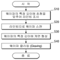
도 4는 본 발명의 일 실시에에 따른 웨이퍼의 시닝 방법의 순서도이다. 또한, 도 5는 도 4의 실시예에 따른 웨이퍼의 시닝 과정을 도시한 개념도이고, 도 6은 도 4의 실시예에 따른 웨이퍼의 시닝 과정 중 클리빙 과정을 더 상세히 도시한 개념도이다. 그리고, 도 7은 도 4의 실시예에 따른 웨이퍼의 시닝 과정에서 형성된 웨이퍼의 격자 라인을 도시한 단면도이다.4 is a flowchart of a method of thinning a wafer according to an embodiment of the present invention. FIG. 5 is a conceptual diagram illustrating a wafer thinning process according to the embodiment of FIG. 4, and FIG. 6 is a conceptual diagram illustrating a cleaving process in detail during wafer thinning according to the embodiment of FIG. FIG. 7 is a cross-sectional view illustrating a lattice line of the wafer formed in the thinning process of the wafer according to the embodiment of FIG.
도 4 내지 도 6을 참조하면, 본 발명의 일 실시에에 따른 웨이퍼의 시닝(Thinning) 방법은, 웨이퍼(50)의 특정 깊이에 초점이 맞추어진 라인빔(60)을 조사하며(S10), 라인빔(60)을 이용하여 웨이퍼(50)를 스캔하여(S20) 상기 웨이퍼(50)의 특정 깊이에 계면(57)을 형성하고(S30), 계면(57)이 형성된 웨이퍼(50)를 패턴 웨이퍼(pattern wafer)와 더미 웨이퍼(dummy wafer)로 클리빙(cleaving)한다(S40). 여기에서, 계면(57)은 웨이퍼(50)의 내부에 있는 클리빙의 기준이 되는 층을 말하고, 패턴 웨이퍼(pattern wafer)과 더미 웨이퍼(dummy wafer)는 각각 클리빙된 웨이퍼에서 회로 패턴(55)을 구비한 웨이퍼와 회로 패턴(55)을 구비하지 않은 웨이퍼를 의미한다.4 to 6, a wafer thinning method according to an embodiment of the present invention irradiates the
즉, 웨이퍼의 시닝 방법은 웨이퍼(50)의 원하는 두께에 따라 특정 깊이에 초점이 맞춰진 레이저 라인빔(60)을 평면방향으로 스캔하여 계면(57)을 형성함으로써 그 평면 층을 기준으로 웨이퍼(50)를 상하로 클리빙(cleaving)하여 간단하게 원하는 두께로 웨이퍼를 떼어내는 것을 특징으로 한다. 그리하여, 짧은 Tact Time으로 고 생산성을 달성함은 물론 기계적인 연마과정을 생략할 수 있으므로 전체 웨이퍼의 두께 변동도 최소화 할 수 있다.That is, the thinning method of the wafer scans the
레이저는 flat top 형태의 라인 빔 광학계를 가질수 있으며, 광학계는 대상 웨이퍼의 사이즈에 맞게 레이저 빔의 사이즈를 변경할 수 있다. 레이저의 초점위치를 웨이퍼의 절단할 깊이에 맞춰 레이저 라인빔(60)을 조사할 수 있다. 이때, 레이저 라인빔(60)은 웨이퍼(50)의 회로 패턴이 형성된 면의 반대면에서 조사된다. 이를 통해 라인빔(60)이 집중되는 웨이퍼(50)의 내부 층 이외에는 열-충격을 최소화할 수 있다. 즉, 웨이퍼(50)를 상하로 클리빙하는 기준이 되는 계면(57) 이외에는 충격을 최소화할 수 있다.The laser may have a line beam optical system in the form of a flat top, and the optical system may change the size of the laser beam to match the size of the target wafer. The
웨이퍼(50)의 특정 깊이에 초점이 맞추어진 라인빔(60)을 조사(S10)하기 위해, 레이저 빔을 조사하고, 상기 조사되는 레이저 빔을 성형하여 라인빔(60)을 생성하게 된다. 이에, 레이저는 라인빔(60)을 생성하기 위해 별도의 라인빔 광학계를 구비할 수 있다.A laser beam is irradiated to form the
또한, 웨이퍼(50)의 특정 깊이에 계면(57)을 형성하는 경우(S30), 라인빔(60)의 스캔 속도 또는 라인빔의(60) 세기 중 적어도 하나를 조정하여, 웨이퍼(50)의 특정 깊이에 격자 모양의 라인을 형성할 수 있다. 도 7에서, 웨이퍼(50)의 평면 상에 원하는 위치에 격자 모양으로 에너지가 선택적으로 추가 인가된 라인이 도시되어 있다. 이런 라인은 웨이퍼(50)를 라인빔(60)으로 스캔한 후, 웨이퍼(50)를 90도로 회전시켜 동일하게 평면방향으로 라인빔(60)을 스캔하여 형성할 수 있다. 그리하여, 웨이퍼(50)의 특정 깊이에는 평면방향으로 계면(57)이 형성됨과 동시에 특정 간격의 격자 모양의 라인도 함께 형성이 된다. 이러한 격자 모양의 라인은 클리빙(Cleaving)공정 후, 패턴 웨이퍼(pattern wafer)의 표면에 남아있게 되고 반도체 조립을 위해 웨이퍼 마운트 필름에 부착되어 다이 본드(Die Bond) 또는 플립칩 본드(Flip Chip Bond) 공정에서 웨이퍼 마운트 필름을 팽창시킬 때에 발생하는 응력에 의해 갈라지는 절단면의 시작점이 된다. 이를 통해, 레이저 라인빔(60)을 스캔하여 웨이퍼(50)를 원하는 두께로 시닝(Thinning)하는 공정과 웨이퍼(50)를 원하는 사이즈로 절단하는 소잉(Sawing) 또는 다이싱(Dicing) 공정을 대체할 수 있다.It is also possible to adjust at least one of the scan speed of the
그리고, 계면(57)이 형성된 웨이퍼(50)를 패턴 웨이퍼(pattern wafer)와 더미 웨이퍼(dummy wafer)로 클리빙(cleaving)하는 경우(S40), 웨이퍼(50)의 양면을 고정하는 이동하는 웨이퍼 척(70, 75)을 반대 방향으로 이동시켜 웨이퍼(50)를 분리할 수 있다. 또한, 웨이퍼(50)의 클리빙을 용이하게 하기 위해, 계면(57)에 기계적인 힘을 가하는 충격부재(80)를 사용할 수 있다.When the
웨이퍼(50)가 패턴 웨이퍼(pattern wafer)와 더미 웨이퍼(dummy wafer)로 클리빙(cleaving)된 후(S40), 원하는 두께로 분리된 패턴 웨이퍼는 분리면을 고르게 하기 위해 폴리싱(polishing) 공정으로 제공되고, 분리된 나머지 더미 웨이퍼는 다시 FAB 공정에 투입되어 새로운 패턴 웨이퍼로 재활용된다. 이에, 불필요한 더미 웨이퍼(50)의 재활용이 가능하다.After the
도 8은 도 4의 실시예에 따른 웨이퍼의 처리 과정을 도시한 개념도이다.FIG. 8 is a conceptual view showing a process of processing wafers according to the embodiment of FIG.
도 8을 참조하면, 웨이퍼 매거진(410)에 수납된 웨이퍼(50)는 웨이퍼 핸들러(Wafer Handler, 400)에 의해 클리빙 공정(Cleaving, 100)으로 제공되어 상기 클리빙 공정(Cleaving, 100)을 마친 웨이퍼(50)는 패턴 웨이퍼(pattern wafer)와 더미 웨이퍼(dummy wafer)로 나누어진다. 그런 후에, 패턴 웨이퍼(pattern wafer)는 웨이퍼 핸들러(400)에 의해 폴리싱 공정(Polishing, 200)으로 제공되어 패턴 웨이퍼의 면을 고르게 한 후, 다시 웨이퍼 핸들러(400)에 의해 패턴 웨이퍼 매거진(420)에 수납된다. 그리고, 더미 웨이퍼(dummy wafer)는 웨이퍼 핸들러(400)에 의해 더미 웨이퍼 매거진(430)에 분리되어 수납되고, 더미 웨이퍼 매거진(430)에 수납된 더미 웨이퍼들은 FAB 공정에 투입되어 새로운 웨이퍼로 재활용된다.8, the
따라서, 원하는 웨이퍼(50)의 두께에 따라 라인빔(60)의 조사 깊이를 변경함으로써 선택적 시닝(Thinning0이 가능하다. 또한, 클리빙(Cleaving)만으로 바로 원하는 두께로 웨이퍼(50)의 시닝(Thinning)이 가능하므로 짧은 공정시간과 함께 오/폐수의 절감과 불필요한 더미 웨이퍼(50)의 재활용이 가능하다. 이를 통해, 웨이퍼(50)의 기계적 스트레스 및 화학적 스트레스를 최소화할 수 있다. 그리고, 웨이퍼(50)의 특정 깊이에는 평면방향으로 계면(57)이 형성됨과 동시에 특정 간격의 격자 모양의 라인도 함께 형성이 됨으로써, 격자 모양의 라인은 클리빙 공정 후, 본딩 공정에서 웨이퍼 마운트 테잎(Wafer Mount Tape)을 확장(Expansion)시킬 때 발생하는 응력에 의해 갈라지는 절단면의 시작점이 되고, 이를 통해 본 웨이퍼(50)를 원하는 두께로 시닝(Thinning)하는 공정과 웨이퍼(50)를 원하는 사이즈로 절단하는 소잉(Sawing)공정을 대체할 수 있다Therefore, it is possible to perform selective thinning by changing the irradiation depth of the
도 9a 및 도 9b는 본 발명의 일 실시에에 따른 웨이퍼의 시닝 장치의 구성도이다.9A and 9B are block diagrams of a wafer thinning apparatus according to an embodiment of the present invention.
본 발명의 일 실시에에 따른 웨이퍼의 시닝 장치(500)는, 웨이퍼(50)의 일면을 지지하고, 고정하는 웨이퍼 지지부(510), 레이저 빔을 조사하는 레이저 광원부(520), 상기 레이저 빔을 성형하여 라인빔을 생성하며, 상기 웨이퍼(50)의 사이즈에 맞추어 상기 웨이퍼(50)의 특정 깊이에 상기 라인빔을 조사하는 라인빔 광학부(530), 상기 라인빔을 이용하여 상기 웨이퍼(50)를 스캔하기 위해 상기 라인빔 광학부(530) 또는 상기 웨이퍼 지지부(510) 중 적어도 하나를 XY축 방향으로 이동시키는 갠트리부(540), 상기 웨이퍼(50)의 타면을 고정하는 웨이퍼 고정부(560), 및 상기 웨이퍼 지지부(510) 및 상기 웨이퍼 고정부(560)를 반대 방향으로 이동시켜, 상기 라인빔의 스캔에 의해 상기 웨이퍼(50)의 특정 깊이에 형성된 계면(57)을 중심으로 상기 웨이퍼(50)를 패턴 웨이퍼(pattern wafer)와 더미 웨이퍼(dummy wafer)로 클리빙(cleaving)하는 클리빙 이동부(570)를 포함한다. 또한, 따른 웨이퍼의 시닝 장치(500)는, 상기 레이저 광원부(510)의 출력을 제어하여 라인빔의 세기를 조정하거나, 또는 갠트리부(540)를 제어하여 상기 라인빔의 스캔 속도를 조정하는 제어부(550)를 포함할 수 있다.A wafer thinning apparatus 500 according to one embodiment of the present invention includes a
웨이퍼 지지부(510)는 웨이퍼(50)의 일면을 지지하는 역할을 하며, 웨이퍼(50)의 클리빙 시에 웨이퍼(50)를 고정하게 된다.The
레이저 광원부(520)는 레이저빔을 공급하며, 레이저 소스는 포톤(photon) 에너지를 가지는 모든 레이저가 포함될 수 있다. 레이저 광원부(520)는 다이오드 레이저, 적외선 레이저, DPSS 레이저, KrF 엑시머 레이저, 나노초 레이저 등 채택 가능한 어떠한 레이저라도 사용가능할 수 있음은 당업자에게 자명하다 할 것이다.The laser
라인빔 광학부(530)는 레이저빔에 대하여 레이저 가공에 요구되는 라인빔의 단면 형상으 가지도록 레이저빔을 광학적으로 성형하는 역할을 한다. 라인빔 광학부(530)는 입사된 레이저빔에 대하여 균일한 세기를 가지면서도 그 단면 형상이 소정의 길이와 폭을 가지도록 레이저빔을 광학적으로 성형한다. 예를 들어, 라인빔 광학부(530)는 필드 조리개로 레이저빔을 포커싱하여 그 단면 형상이 장방형인 라인빔을 생성할 수 있다. 또는, 입사된 하나의 원형 스팟을 가지는 레이저빔에 대하여 이웃하는 스팟 사이에 소정의 간격을 가지도록 복수의 레이저빔만큼 증가시켜 초점면에서 복수의 원형 스팟이 일렬로 배치되도록 할 수 있고, 복수의 원형 스팟 일부가 서로 중첩되어 가우스형 세기 분포를 일차원 방향에서 flat-top 시킨 라인빔으로 생성할 수도 있다. 이외에도, 레이점빔을 라인빔으로 성형하는 다른 방식이 적용될 수도 있음은 당업자에게 자명하다 할 것이다.The line beam
갠트리부(540)는 라인빔으로 웨이퍼(50)를 스캔하는 역할을 하며, 웨이퍼(50)를 스캔하기 위해 라인빔 광학부(530) 또는 웨이퍼 지지부(510) 중 적어도 하나를 XY축 방향으로 이동시킬 수 있다. 갠트리부(540)에 의해, 웨이퍼(50)의 소정 깊이의 2차원 평면을 라인빔으로 상하 좌우 스캔할 수 있다.The
제어부(550)는 레이저 광원부(510)의 출력을 제어하여 라인빔의 세기를 조정하거나, 또는 갠트리부(540)를 제어하여 라인빔의 스캔 속도를 조정함으로써, 스캔되는 웨이퍼(50)의 내부 평면 상에 원하는 위치에 격자 모양의 라인(Line) 형상으로 에너지가 선택적으로 추가 인가된 선을 그을 수가 있다. 그리하여, 웨이퍼(50)의 특정 깊이에는 평면 방향으로 계면이 형성됨과 동시에 특정 간격의 격자모양의 라인도 함께 형성이 된다The
웨이퍼 고정부(560)는 웨이퍼 지지부(510)의 반대편에서 웨이퍼(50)의 타면을 고정하는 역할을 하며, 웨이퍼 고정부(560)와 웨이퍼 지지부(510)가 웨이퍼(50)의 양면을 고정하고, 웨이퍼 고정부(560)와 웨이퍼 지지부(510)를 서로 반대방향으로 이동시켜 웨이퍼(50)를 원하는 두께로 클리빙을 할 수가 있다.The
클리빙 이동부(570)는 웨이퍼 고정부(560)와 웨이퍼 지지부(510)를 서로 반대방향으로 이동시키는 구동력을 제공하며, 클리빙 이동부(570)의 동작에 의해 웨이퍼(50)가 웨이퍼(50)의 특정 깊이에 형성된 계면(57)을 중심으로 패턴 웨이퍼(pattern wafer)와 더미 웨이퍼(dummy wafer)로 쪼개진다.The
따라서, 본 발명의 일 실시에에 따른 웨이퍼의 시닝 장치(500)에 의해, 웨이퍼(50)를 레이저 라인빔(Laser Line Beam)으로 스캔하여, 웨이퍼(50)를 원하는 두께로 시닝(Thinning)하고, 웨이퍼(50)를 원하는 다이 사이즈로 절단하는 다이싱(Dicing)을 대체할 수 있고, 이에 따라 웨이퍼(50)의 기계적 스트레스 및 화학적 스트레스를 최소화할 수 있다.Therefore, the
이상 첨부된 도면을 참조하여 본 발명의 실시예를 설명하였지만, 본 발명이 속하는 기술분야에서 통상의 지식을 가진 자는 본 발명이 그 기술적 사상이나 필수적인 특징을 변경하지 않고서 다른 구체적인 형태로 실시될 수 있다는 것을 이해할 수 있을 것이다. 그러므로 이상에서 기술한 실시예들은 모든 면에서 예시적인 것이며 한정적이 아닌 것으로 이해해야만 한다.While the present invention has been described in connection with what is presently considered to be practical exemplary embodiments, it is to be understood that the invention is not limited to the disclosed embodiments, but, on the contrary, You will understand. It is therefore to be understood that the above-described embodiments are illustrative in all aspects and not restrictive.
50: 웨이퍼 55: 회로 패턴
57: 계면 70, 75: 웨이퍼 척
100, 300: 클리빙 공정(Cleaving)
200: 폴리싱 공정(Polishing)
400: 웨이퍼 핸들러
500: 웨이퍼의 시닝 장치
510: 웨이퍼 지지부 520: 레이저 광원부
530: 라인빔 광학부 540: 갠트리부
550: 제어부 560: 웨이퍼 고정부
570: 클리빙 이동부50: wafer 55: circuit pattern
57:
100, 300: Cleaving process (Cleaving)
200: Polishing process
400: Wafer handler
500: wafer thinning device
510: Wafer supporter 520: Laser beam source
530: Line beam optical part 540: Gantry part
550: Control section 560: Wafer fixing section
570: Cleaving moving part
Claims (6)
상기 라인빔을 이용하여 상기 웨이퍼를 스캔하여 상기 웨이퍼의 특정 깊이에 상기 웨이퍼와 평행한 계면을 형성함과 동시에, 상기 라인빔의 스캔 속도 또는 상기 라인빔의 세기 중 적어도 하나를 조정하여 상기 웨이퍼에 수직인 방향으로 격자 모양의 라인을 형성하는 단계;
상기 계면을 경계로 상기 웨이퍼를 패턴 웨이퍼(pattern wafer)와 더미 웨이퍼(dummy wafer)로 클리빙(cleaving)하는 단계; 및
상기 격자 모양의 라인을 경계로 상기 패턴 웨이퍼를 다이싱하는 단계를 포함하는, 웨이퍼의 시닝 방법.Irradiating a line beam focused on a specific depth of a wafer, the line beam having a uniform intensity along the line, the cross-sectional shape of the line beam having a specific length and width;
Scanning the wafer using the line beam to form an interface parallel to the wafer at a specific depth of the wafer and adjusting at least one of the scan speed of the line beam or the intensity of the line beam, Forming a grid-like line in a perpendicular direction;
Cleaving the wafer with a pattern wafer and a dummy wafer with the interface as a boundary; And
And dicing the pattern wafer with the grid-like line as a boundary.
상기 라인빔을 조사하는 단계는,
레이저 빔을 조사하는 단계; 및
상기 레이저 빔을 성형하여 상기 라인빔을 생성하는 단계를 포함하는, 웨이퍼의 시닝 방법.The method according to claim 1,
Wherein the step of illuminating the line beam comprises:
Irradiating a laser beam; And
And shaping the laser beam to produce the line beam.
상기 더미 웨이퍼에 회로 패턴을 형성하여 재활용하는 단계를 더 포함하는, 웨이퍼의 시닝 방법.The method according to claim 1,
Forming a circuit pattern on said dummy wafer and recycling said wafer.
레이저 빔을 조사하는 레이저 광원부;
상기 레이저 빔을 성형하여 라인빔을 생성하며, 상기 웨이퍼의 사이즈에 맞추어 상기 웨이퍼의 특정 깊이에 상기 라인빔을 조사하되, 상기 라인빔은 라인을 따라 균일한 세기를 가지면서 그 단면 형상이 특정 길이와 폭을 갖는 라인빔 광학부;
상기 라인빔을 이용하여 상기 웨이퍼를 스캔하기 위해 상기 라인빔 광학부 또는 상기 웨이퍼 지지부 중 적어도 하나를 XY축 방향으로 이동시키는 갠트리부;
상기 웨이퍼의 타면을 고정하는 웨이퍼 고정부;
상기 웨이퍼 지지부 및 상기 웨이퍼 고정부를 반대 방향으로 이동시켜, 상기 라인빔의 스캔에 의해 상기 웨이퍼의 특정 깊이에 상기 웨이퍼와 평행하게 형성된 계면을 중심으로 상기 웨이퍼를 패턴 웨이퍼(pattern wafer)와 더미 웨이퍼(dummy wafer)로 클리빙(cleaving)하는 클리빙 이동부; 및
상기 계면이 형성될 때 상기 계면의 형성과 동시에 상기 웨이퍼와 수직인 방향으로 격자 모양 라인을 형성하기 위해, 상기 레이저 광원부의 출력을 제어하여 상기 라인빔의 세기를 조정하거나 상기 갠트리부를 제어하여 상기 라인빔의 스캔 속도를 조정하는 제어부;를 포함하는, 웨이퍼의 시닝 장치.A wafer support for supporting and fixing one surface of the wafer;
A laser light source unit for irradiating a laser beam;
Forming a line beam on the wafer to form a line beam; irradiating the line beam to a specific depth of the wafer in accordance with the size of the wafer, the line beam having uniform intensity along the line, A line beam optical portion having a width and a width;
A gantry unit for moving at least one of the line beam optical unit or the wafer support unit in the XY axis direction to scan the wafer using the line beam;
A wafer fixing part for fixing the other surface of the wafer;
The wafer support portion and the wafer fixing portion are moved in opposite directions so that the wafer is transferred to the pattern wafer and the dummy wafer at a predetermined depth of the wafer by scanning the line beam, a cleaving moving part for cleaving with a dummy wafer; And
And controlling the intensity of the line beam by controlling the output of the laser light source unit or controlling the gantry unit to form a lattice line in a direction perpendicular to the wafer at the time of forming the interface when the interface is formed, And a control unit for adjusting the scan speed of the beam.
Priority Applications (4)
| Application Number | Priority Date | Filing Date | Title |
|---|---|---|---|
| KR1020130043080A KR101803790B1 (en) | 2013-04-18 | 2013-04-18 | Thinning method and apparatus of wafer |
| JP2016508855A JP6105808B2 (en) | 2013-04-18 | 2014-04-02 | Wafer thinning method and apparatus |
| PCT/KR2014/002808 WO2014171649A1 (en) | 2013-04-18 | 2014-04-02 | Method and apparatus for thinning wafer |
| US14/785,372 US10319598B2 (en) | 2013-04-18 | 2014-04-02 | Method and apparatus for thinning wafer |
Applications Claiming Priority (1)
| Application Number | Priority Date | Filing Date | Title |
|---|---|---|---|
| KR1020130043080A KR101803790B1 (en) | 2013-04-18 | 2013-04-18 | Thinning method and apparatus of wafer |
Publications (2)
| Publication Number | Publication Date |
|---|---|
| KR20140125474A KR20140125474A (en) | 2014-10-29 |
| KR101803790B1 true KR101803790B1 (en) | 2017-12-04 |
Family
ID=51731550
Family Applications (1)
| Application Number | Title | Priority Date | Filing Date |
|---|---|---|---|
| KR1020130043080A Active KR101803790B1 (en) | 2013-04-18 | 2013-04-18 | Thinning method and apparatus of wafer |
Country Status (4)
| Country | Link |
|---|---|
| US (1) | US10319598B2 (en) |
| JP (1) | JP6105808B2 (en) |
| KR (1) | KR101803790B1 (en) |
| WO (1) | WO2014171649A1 (en) |
Families Citing this family (12)
| Publication number | Priority date | Publication date | Assignee | Title |
|---|---|---|---|---|
| WO2015098595A1 (en) * | 2013-12-27 | 2015-07-02 | 旭硝子株式会社 | Method for processing brittle plate, and device for processing brittle plate |
| CN105924478B (en) * | 2016-05-24 | 2018-05-29 | 济南大学 | A kind of preparation method of three-dimensional paper substrate metal organic frame |
| JP6858587B2 (en) * | 2017-02-16 | 2021-04-14 | 株式会社ディスコ | Wafer generation method |
| KR102046871B1 (en) * | 2017-08-25 | 2019-11-21 | 세메스 주식회사 | Substrate treating apparatus and substrate treating method |
| WO2020066492A1 (en) * | 2018-09-25 | 2020-04-02 | 東京エレクトロン株式会社 | Substrate processing system and substrate processing method |
| US12020936B2 (en) * | 2018-12-21 | 2024-06-25 | Tokyo Electron Limited | Substrate processing apparatus and substrate processing method |
| JP7109590B2 (en) * | 2018-12-21 | 2022-07-29 | 東京エレクトロン株式会社 | SUBSTRATE PROCESSING APPARATUS AND SUBSTRATE PROCESSING METHOD |
| CN116213967A (en) * | 2018-12-21 | 2023-06-06 | 东京毅力科创株式会社 | Peripheral edge removal device and peripheral edge removal method |
| JP7129558B2 (en) * | 2019-04-19 | 2022-09-01 | 東京エレクトロン株式会社 | Processing equipment and processing method |
| US11682600B2 (en) | 2019-08-07 | 2023-06-20 | At&S Austria Technologie & Systemtechnik Aktiengesellschaft | Protection layer for panel handling systems |
| EP4291006A3 (en) * | 2022-05-16 | 2023-12-27 | Samsung Display Co., Ltd. | Display device, electronic device including the same, and method of manufacturing the display device |
| DE102023108751B3 (en) * | 2023-04-05 | 2024-05-29 | Infineon Technologies Ag | METHOD FOR SEPARATING DIE FROM A SEMICONDUCTOR SUBSTRATE |
Citations (2)
| Publication number | Priority date | Publication date | Assignee | Title |
|---|---|---|---|---|
| KR200373909Y1 (en) * | 2004-10-25 | 2005-01-26 | 손진호 | Adjustable laser-beam length laser projector |
| JP2012169363A (en) * | 2011-02-10 | 2012-09-06 | Saitama Univ | Substrate processing method |
Family Cites Families (11)
| Publication number | Priority date | Publication date | Assignee | Title |
|---|---|---|---|---|
| JP2002075917A (en) | 2000-08-25 | 2002-03-15 | Canon Inc | Sample separation apparatus and separation method |
| US7811900B2 (en) | 2006-09-08 | 2010-10-12 | Silicon Genesis Corporation | Method and structure for fabricating solar cells using a thick layer transfer process |
| JP5442224B2 (en) * | 2007-07-23 | 2014-03-12 | 株式会社半導体エネルギー研究所 | Manufacturing method of SOI substrate |
| JP4998210B2 (en) * | 2007-10-31 | 2012-08-15 | 三菱電機株式会社 | Manufacturing method of semiconductor light emitting device |
| US20090212397A1 (en) * | 2008-02-22 | 2009-08-27 | Mark Ewing Tuttle | Ultrathin integrated circuit and method of manufacturing an ultrathin integrated circuit |
| JP2009290052A (en) | 2008-05-30 | 2009-12-10 | Disco Abrasive Syst Ltd | Method of dividing wafer |
| JP2010021398A (en) | 2008-07-11 | 2010-01-28 | Disco Abrasive Syst Ltd | Method of treating wafer |
| US7867876B2 (en) | 2008-12-23 | 2011-01-11 | International Business Machines Corporation | Method of thinning a semiconductor substrate |
| US20110132885A1 (en) | 2009-12-07 | 2011-06-09 | J.P. Sercel Associates, Inc. | Laser machining and scribing systems and methods |
| WO2012108052A1 (en) * | 2011-02-10 | 2012-08-16 | 信越ポリマー株式会社 | Monocrystalline substrate production method and monocrystalline member with modified layer formed therein |
| KR20130033114A (en) | 2011-09-26 | 2013-04-03 | 주식회사 이오테크닉스 | Laser processing method |
-
2013
- 2013-04-18 KR KR1020130043080A patent/KR101803790B1/en active Active
-
2014
- 2014-04-02 JP JP2016508855A patent/JP6105808B2/en active Active
- 2014-04-02 WO PCT/KR2014/002808 patent/WO2014171649A1/en not_active Ceased
- 2014-04-02 US US14/785,372 patent/US10319598B2/en active Active
Patent Citations (2)
| Publication number | Priority date | Publication date | Assignee | Title |
|---|---|---|---|---|
| KR200373909Y1 (en) * | 2004-10-25 | 2005-01-26 | 손진호 | Adjustable laser-beam length laser projector |
| JP2012169363A (en) * | 2011-02-10 | 2012-09-06 | Saitama Univ | Substrate processing method |
Also Published As
| Publication number | Publication date |
|---|---|
| JP2016519433A (en) | 2016-06-30 |
| US20160064229A1 (en) | 2016-03-03 |
| KR20140125474A (en) | 2014-10-29 |
| US10319598B2 (en) | 2019-06-11 |
| JP6105808B2 (en) | 2017-03-29 |
| WO2014171649A1 (en) | 2014-10-23 |
Similar Documents
| Publication | Publication Date | Title |
|---|---|---|
| KR101803790B1 (en) | Thinning method and apparatus of wafer | |
| US8466074B2 (en) | Method for processing a substrate using a laser beam | |
| CN100466184C (en) | wafer processing method | |
| JP5904720B2 (en) | Wafer division method | |
| KR102096674B1 (en) | Wafer machining method | |
| JP5162163B2 (en) | Wafer laser processing method | |
| KR101121495B1 (en) | Method and apparatus for dividing plate-like member | |
| JP6219904B2 (en) | Laser fiber array for separating semiconductor wafers | |
| JP6224653B2 (en) | Thin semiconductor substrate dicing method | |
| US20060035444A1 (en) | Wafer dividing method | |
| CN100419996C (en) | Wafer Separation Method | |
| KR101160200B1 (en) | Method for Dividing Wafers | |
| CN101436526A (en) | Method of manufacturing semiconductor device | |
| KR102399375B1 (en) | Wafer processing method | |
| JP2014019120A (en) | Method of manufacturing single crystal member for forming internal processing layer | |
| JP6202696B2 (en) | Single crystal substrate manufacturing method | |
| JP6953210B2 (en) | Wafer processing method | |
| JP2024042769A (en) | Chip manufacturing method | |
| JP6012185B2 (en) | Manufacturing method of semiconductor device | |
| CN107799406B (en) | Method for processing wafer and method for processing carrier | |
| TWI868313B (en) | Chip manufacturing method | |
| JP5969214B2 (en) | Manufacturing method of semiconductor device | |
| JP2011171382A (en) | Dividing method | |
| JP2006059941A (en) | Manufacturing method of semiconductor chip | |
| KR20130033113A (en) | Laser processing method |
Legal Events
| Date | Code | Title | Description |
|---|---|---|---|
| PA0109 | Patent application |
St.27 status event code: A-0-1-A10-A12-nap-PA0109 |
|
| PG1501 | Laying open of application |
St.27 status event code: A-1-1-Q10-Q12-nap-PG1501 |
|
| PN2301 | Change of applicant |
St.27 status event code: A-3-3-R10-R13-asn-PN2301 St.27 status event code: A-3-3-R10-R11-asn-PN2301 |
|
| A201 | Request for examination | ||
| PA0201 | Request for examination |
St.27 status event code: A-1-2-D10-D11-exm-PA0201 |
|
| E902 | Notification of reason for refusal | ||
| PE0902 | Notice of grounds for rejection |
St.27 status event code: A-1-2-D10-D21-exm-PE0902 |
|
| E13-X000 | Pre-grant limitation requested |
St.27 status event code: A-2-3-E10-E13-lim-X000 |
|
| P11-X000 | Amendment of application requested |
St.27 status event code: A-2-2-P10-P11-nap-X000 |
|
| P13-X000 | Application amended |
St.27 status event code: A-2-2-P10-P13-nap-X000 |
|
| R18-X000 | Changes to party contact information recorded |
St.27 status event code: A-3-3-R10-R18-oth-X000 |
|
| E902 | Notification of reason for refusal | ||
| PE0902 | Notice of grounds for rejection |
St.27 status event code: A-1-2-D10-D21-exm-PE0902 |
|
| P11-X000 | Amendment of application requested |
St.27 status event code: A-2-2-P10-P11-nap-X000 |
|
| P13-X000 | Application amended |
St.27 status event code: A-2-2-P10-P13-nap-X000 |
|
| E701 | Decision to grant or registration of patent right | ||
| PE0701 | Decision of registration |
St.27 status event code: A-1-2-D10-D22-exm-PE0701 |
|
| GRNT | Written decision to grant | ||
| PR0701 | Registration of establishment |
St.27 status event code: A-2-4-F10-F11-exm-PR0701 |
|
| PR1002 | Payment of registration fee |
St.27 status event code: A-2-2-U10-U11-oth-PR1002 Fee payment year number: 1 |
|
| PG1601 | Publication of registration |
St.27 status event code: A-4-4-Q10-Q13-nap-PG1601 |
|
| R18-X000 | Changes to party contact information recorded |
St.27 status event code: A-5-5-R10-R18-oth-X000 |
|
| P22-X000 | Classification modified |
St.27 status event code: A-4-4-P10-P22-nap-X000 |
|
| PN2301 | Change of applicant |
St.27 status event code: A-5-5-R10-R11-asn-PN2301 |
|
| PN2301 | Change of applicant |
St.27 status event code: A-5-5-R10-R14-asn-PN2301 |
|
| PR1001 | Payment of annual fee |
St.27 status event code: A-4-4-U10-U11-oth-PR1001 Fee payment year number: 4 |
|
| PR1001 | Payment of annual fee |
St.27 status event code: A-4-4-U10-U11-oth-PR1001 Fee payment year number: 5 |
|
| PR1001 | Payment of annual fee |
St.27 status event code: A-4-4-U10-U11-oth-PR1001 Fee payment year number: 6 |
|
| PR1001 | Payment of annual fee |
St.27 status event code: A-4-4-U10-U11-oth-PR1001 Fee payment year number: 7 |
|
| PR1001 | Payment of annual fee |
St.27 status event code: A-4-4-U10-U11-oth-PR1001 Fee payment year number: 8 |
|
| PN2301 | Change of applicant |
St.27 status event code: A-5-5-R10-R13-asn-PN2301 St.27 status event code: A-5-5-R10-R11-asn-PN2301 |
|
| P22-X000 | Classification modified |
St.27 status event code: A-4-4-P10-P22-nap-X000 |