KR101719089B1 - 광전 변환 소자 및 그 사용 방법, 광 센서, 촬상 소자 - Google Patents
광전 변환 소자 및 그 사용 방법, 광 센서, 촬상 소자 Download PDFInfo
- Publication number
- KR101719089B1 KR101719089B1 KR1020157026609A KR20157026609A KR101719089B1 KR 101719089 B1 KR101719089 B1 KR 101719089B1 KR 1020157026609 A KR1020157026609 A KR 1020157026609A KR 20157026609 A KR20157026609 A KR 20157026609A KR 101719089 B1 KR101719089 B1 KR 101719089B1
- Authority
- KR
- South Korea
- Prior art keywords
- photoelectric conversion
- ring
- substituent
- group
- compound
- Prior art date
- Legal status (The legal status is an assumption and is not a legal conclusion. Google has not performed a legal analysis and makes no representation as to the accuracy of the status listed.)
- Active
Links
Images


Classifications
-
- H01L51/424—
-
- C—CHEMISTRY; METALLURGY
- C07—ORGANIC CHEMISTRY
- C07D—HETEROCYCLIC COMPOUNDS
- C07D221/00—Heterocyclic compounds containing six-membered rings having one nitrogen atom as the only ring hetero atom, not provided for by groups C07D211/00 - C07D219/00
- C07D221/02—Heterocyclic compounds containing six-membered rings having one nitrogen atom as the only ring hetero atom, not provided for by groups C07D211/00 - C07D219/00 condensed with carbocyclic rings or ring systems
- C07D221/04—Ortho- or peri-condensed ring systems
- C07D221/18—Ring systems of four or more rings
-
- H01L27/307—
-
- H01L31/10—
-
- H01L51/0053—
-
- H01L51/0058—
-
- H01L51/006—
-
- H01L51/4253—
-
- H—ELECTRICITY
- H10—SEMICONDUCTOR DEVICES; ELECTRIC SOLID-STATE DEVICES NOT OTHERWISE PROVIDED FOR
- H10K—ORGANIC ELECTRIC SOLID-STATE DEVICES
- H10K85/00—Organic materials used in the body or electrodes of devices covered by this subclass
- H10K85/40—Organosilicon compounds, e.g. TIPS pentacene
-
- H—ELECTRICITY
- H10—SEMICONDUCTOR DEVICES; ELECTRIC SOLID-STATE DEVICES NOT OTHERWISE PROVIDED FOR
- H10K—ORGANIC ELECTRIC SOLID-STATE DEVICES
- H10K85/00—Organic materials used in the body or electrodes of devices covered by this subclass
- H10K85/60—Organic compounds having low molecular weight
- H10K85/615—Polycyclic condensed aromatic hydrocarbons, e.g. anthracene
- H10K85/626—Polycyclic condensed aromatic hydrocarbons, e.g. anthracene containing more than one polycyclic condensed aromatic rings, e.g. bis-anthracene
-
- H—ELECTRICITY
- H10—SEMICONDUCTOR DEVICES; ELECTRIC SOLID-STATE DEVICES NOT OTHERWISE PROVIDED FOR
- H10K—ORGANIC ELECTRIC SOLID-STATE DEVICES
- H10K85/00—Organic materials used in the body or electrodes of devices covered by this subclass
- H10K85/60—Organic compounds having low molecular weight
- H10K85/631—Amine compounds having at least two aryl rest on at least one amine-nitrogen atom, e.g. triphenylamine
- H10K85/633—Amine compounds having at least two aryl rest on at least one amine-nitrogen atom, e.g. triphenylamine comprising polycyclic condensed aromatic hydrocarbons as substituents on the nitrogen atom
-
- H—ELECTRICITY
- H10—SEMICONDUCTOR DEVICES; ELECTRIC SOLID-STATE DEVICES NOT OTHERWISE PROVIDED FOR
- H10K—ORGANIC ELECTRIC SOLID-STATE DEVICES
- H10K85/00—Organic materials used in the body or electrodes of devices covered by this subclass
- H10K85/60—Organic compounds having low molecular weight
- H10K85/649—Aromatic compounds comprising a hetero atom
- H10K85/654—Aromatic compounds comprising a hetero atom comprising only nitrogen as heteroatom
-
- H—ELECTRICITY
- H10—SEMICONDUCTOR DEVICES; ELECTRIC SOLID-STATE DEVICES NOT OTHERWISE PROVIDED FOR
- H10K—ORGANIC ELECTRIC SOLID-STATE DEVICES
- H10K85/00—Organic materials used in the body or electrodes of devices covered by this subclass
- H10K85/60—Organic compounds having low molecular weight
- H10K85/649—Aromatic compounds comprising a hetero atom
- H10K85/655—Aromatic compounds comprising a hetero atom comprising only sulfur as heteroatom
-
- H—ELECTRICITY
- H10—SEMICONDUCTOR DEVICES; ELECTRIC SOLID-STATE DEVICES NOT OTHERWISE PROVIDED FOR
- H10K—ORGANIC ELECTRIC SOLID-STATE DEVICES
- H10K85/00—Organic materials used in the body or electrodes of devices covered by this subclass
- H10K85/60—Organic compounds having low molecular weight
- H10K85/649—Aromatic compounds comprising a hetero atom
- H10K85/657—Polycyclic condensed heteroaromatic hydrocarbons
- H10K85/6572—Polycyclic condensed heteroaromatic hydrocarbons comprising only nitrogen in the heteroaromatic polycondensed ring system, e.g. phenanthroline or carbazole
-
- H—ELECTRICITY
- H10—SEMICONDUCTOR DEVICES; ELECTRIC SOLID-STATE DEVICES NOT OTHERWISE PROVIDED FOR
- H10K—ORGANIC ELECTRIC SOLID-STATE DEVICES
- H10K85/00—Organic materials used in the body or electrodes of devices covered by this subclass
- H10K85/60—Organic compounds having low molecular weight
- H10K85/649—Aromatic compounds comprising a hetero atom
- H10K85/657—Polycyclic condensed heteroaromatic hydrocarbons
- H10K85/6574—Polycyclic condensed heteroaromatic hydrocarbons comprising only oxygen in the heteroaromatic polycondensed ring system, e.g. cumarine dyes
-
- H01L2031/0344—
-
- H—ELECTRICITY
- H10—SEMICONDUCTOR DEVICES; ELECTRIC SOLID-STATE DEVICES NOT OTHERWISE PROVIDED FOR
- H10K—ORGANIC ELECTRIC SOLID-STATE DEVICES
- H10K30/00—Organic devices sensitive to infrared radiation, light, electromagnetic radiation of shorter wavelength or corpuscular radiation
- H10K30/80—Constructional details
- H10K30/81—Electrodes
- H10K30/82—Transparent electrodes, e.g. indium tin oxide [ITO] electrodes
-
- H—ELECTRICITY
- H10—SEMICONDUCTOR DEVICES; ELECTRIC SOLID-STATE DEVICES NOT OTHERWISE PROVIDED FOR
- H10K—ORGANIC ELECTRIC SOLID-STATE DEVICES
- H10K39/00—Integrated devices, or assemblies of multiple devices, comprising at least one organic radiation-sensitive element covered by group H10K30/00
- H10K39/30—Devices controlled by radiation
- H10K39/32—Organic image sensors
-
- H—ELECTRICITY
- H10—SEMICONDUCTOR DEVICES; ELECTRIC SOLID-STATE DEVICES NOT OTHERWISE PROVIDED FOR
- H10K—ORGANIC ELECTRIC SOLID-STATE DEVICES
- H10K85/00—Organic materials used in the body or electrodes of devices covered by this subclass
- H10K85/60—Organic compounds having low molecular weight
- H10K85/615—Polycyclic condensed aromatic hydrocarbons, e.g. anthracene
- H10K85/621—Aromatic anhydride or imide compounds, e.g. perylene tetra-carboxylic dianhydride or perylene tetracarboxylic di-imide
-
- Y—GENERAL TAGGING OF NEW TECHNOLOGICAL DEVELOPMENTS; GENERAL TAGGING OF CROSS-SECTIONAL TECHNOLOGIES SPANNING OVER SEVERAL SECTIONS OF THE IPC; TECHNICAL SUBJECTS COVERED BY FORMER USPC CROSS-REFERENCE ART COLLECTIONS [XRACs] AND DIGESTS
- Y02—TECHNOLOGIES OR APPLICATIONS FOR MITIGATION OR ADAPTATION AGAINST CLIMATE CHANGE
- Y02E—REDUCTION OF GREENHOUSE GAS [GHG] EMISSIONS, RELATED TO ENERGY GENERATION, TRANSMISSION OR DISTRIBUTION
- Y02E10/00—Energy generation through renewable energy sources
- Y02E10/50—Photovoltaic [PV] energy
- Y02E10/549—Organic PV cells
Landscapes
- Chemical & Material Sciences (AREA)
- Engineering & Computer Science (AREA)
- Materials Engineering (AREA)
- Physics & Mathematics (AREA)
- Spectroscopy & Molecular Physics (AREA)
- Organic Chemistry (AREA)
- Light Receiving Elements (AREA)
- Solid State Image Pick-Up Elements (AREA)
- Electroluminescent Light Sources (AREA)
- Other In-Based Heterocyclic Compounds (AREA)
- Indole Compounds (AREA)
Abstract
Description
도 2 는 촬상 소자의 1 화소분의 단면 모식도이다.
도 3 은 (2) 의 화합물의 1H-NMR 스펙트럼도이다.
도 4 는 (5) 의 화합물의 1H-NMR 스펙트럼도이다.


11 : 하부 전극 (도전성막)
12 : 광전 변환막
15 : 상부 전극 (투명 도전성막)
16A : 전자 블로킹층
16B : 정공 블로킹층
100 : 촬상 소자
101 : 기판
102 : 절연층
103 : 접속 전극
104 : 화소 전극 (하부 전극)
105 : 접속부
106 : 접속부
107 : 광전 변환막
108 : 대향 전극 (상부 전극)
109 : 완충층
110 : 봉지층
111 : 컬러 필터 (CF)
112 : 격벽
113 : 차광층
114 : 보호층
115 : 대향 전극 전압 공급부
116 : 판독 회로
Claims (17)
- 도전성막과, 광전 변환 재료를 함유하는 광전 변환막과, 투명 도전성막을 이 순서로 구비하고,
상기 광전 변환 재료가, 하기 식 (1) 로 나타내는 화합물 (A) 을 함유하는 광전 변환 소자.
[화학식 1]
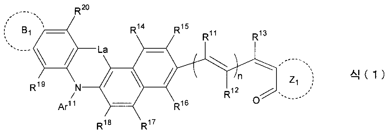
(식 (1) 중, R11 ∼ R13 은, 각각 독립적으로 수소 원자 또는 치환기를 나타낸다. n 은 0 이상의 정수를 나타낸다. R11 과 R12, R11 과 R13 은, 각각 서로 결합하여 고리를 형성해도 된다. n 이 2 이상인 경우, 복수의 R11 끼리, 복수의 R12 끼리는, 각각 서로 결합하여 고리를 형성해도 된다.
R14 ∼ R20 은, 각각 독립적으로 수소 원자 또는 치환기를 나타낸다.
Ar11 은, 치환기를 가져도 되는, 아릴기 또는 헤테로아릴기를 나타낸다. Ar11 상의 치환기는, R18 또는 R19 와 서로 결합하여 고리를 형성해도 된다.
La 는, >CR1aR1b, >NR1c, 치환기를 가져도 되는 알케닐렌기, -O-, -S-, 및 >SiR1dR1e 로 이루어지는 군에서 선택되는 기를 나타낸다. 여기서, R1a, R1b, R1c, R1d 및 R1e 는, 각각 독립적으로 수소 원자 또는 치환기를 나타낸다.
Z1 은, 적어도 2 개의 탄소 원자를 함유하는 고리로서, 5 원자 고리, 6 원자 고리, 또는 5 원자 고리 및 6 원자 고리 중 적어도 어느 것을 포함하는 축합 고리를 나타낸다.
B1 은, 치환기를 가져도 되는, 5 원자 고리 또는 6 원자 고리를 나타낸다. B1 은, 추가로 축환 구조를 가져도 된다.) - 제 1 항에 있어서,
상기 식 (1) 중의 Z1 이, 하기 식 (Z1) 로 나타내는 고리인 광전 변환 소자.
[화학식 2]
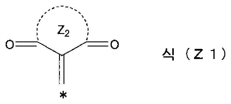
(식 (Z1) 중, Z2 는, 적어도 3 개의 탄소 원자를 함유하는 고리로서, 5 원자 고리, 6 원자 고리, 또는 5 원자 고리 및 6 원자 고리 중 적어도 어느 것을 포함하는 축합 고리를 나타낸다. * 는, 상기 식 (1) 중의 R13 이 결합하고 있는 탄소 원자와의 결합 위치를 나타낸다.) - 제 1 항 또는 제 2 항에 있어서,
상기 식 (1) 중의 Ar11 이, 치환기를 가져도 되는 아릴기인 광전 변환 소자. - 제 1 항 또는 제 2 항에 있어서,
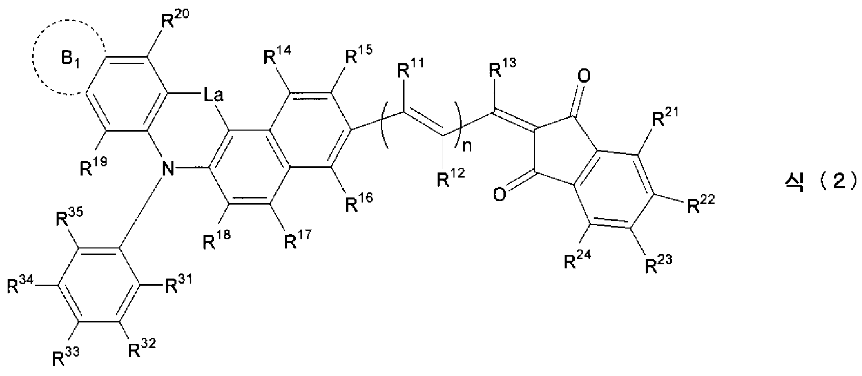
상기 화합물 (A) 이, 하기 식 (2) 로 나타내는 화합물 (a1) 인 광전 변환 소자.
[화학식 3]

(식 (2) 중, R11 ∼ R13 은, 각각 독립적으로 수소 원자 또는 치환기를 나타낸다. n 은 0 이상의 정수를 나타낸다. R11 과 R12, R11 과 R13 은, 각각 서로 결합하여 고리를 형성해도 된다. n 이 2 이상인 경우, 복수의 R11 끼리, 복수의 R12 끼리는, 각각 서로 결합하여 고리를 형성해도 된다.
R14 ∼ R20 은, 각각 독립적으로 수소 원자 또는 치환기를 나타낸다.
R21 ∼ R24 는, 각각 독립적으로 수소 원자 또는 치환기를 나타낸다. R21 과 R22, R22 와 R23, R23 과 R24 는, 각각 서로 결합하여 고리를 형성해도 된다.
R31 ∼ R35 는, 각각 독립적으로 수소 원자 또는 치환기를 나타낸다. R31 과 R32, R32 와 R33, R33 과 R34, R34 와 R35 는, 각각 서로 결합하여 고리를 형성해도 된다.
La 는, >CR1aR1b, >NR1c, 치환기를 가져도 되는 알케닐렌기, -O-, -S-, 및 >SiR1dR1e 로 이루어지는 군에서 선택되는 기를 나타낸다. 여기서, R1a, R1b, R1c, R1d 및 R1e 는, 각각 독립적으로 수소 원자 또는 치환기를 나타낸다.
B1 은, 치환기를 가져도 되는, 5 원자 고리 또는 6 원자 고리를 나타낸다. B1 은, 추가로 축환 구조를 가져도 된다.) - 제 4 항에 있어서,
상기 식 (2) 중의 n 이 0 인 광전 변환 소자. - 제 4 항에 있어서,
상기 식 (2) 중의 La 가 >CR1aR1b (여기서, R1a 및 R1b 는, 각각 독립적으로 수소 원자 또는 탄화수소기를 나타낸다) 로 나타내는 기인 광전 변환 소자. - 제 4 항에 있어서,
상기 화합물 (a1) 이, 하기 식 (3) 으로 나타내는 화합물 (a2) 인 광전 변환 소자.
[화학식 4]

(식 (3) 중, R14 ∼ R20 은, 각각 독립적으로 수소 원자 또는 치환기를 나타낸다.
R21 ∼ R24 는, 각각 독립적으로 수소 원자 또는 치환기를 나타낸다. R21 과 R22, R22 와 R23, R23 과 R24 는, 각각 서로 결합하여 고리를 형성해도 된다.
R31 ∼ R35 는, 각각 독립적으로 수소 원자 또는 치환기를 나타낸다. R31 과 R32, R32 와 R33, R33 과 R34, R34 와 R35 는, 각각 서로 결합하여 고리를 형성해도 된다.
R36 ∼ R39 는, 각각 독립적으로 수소 원자 또는 치환기를 나타낸다. R36 과 R37, R37 과 R38, R38 과 R39 는, 각각 서로 결합하여 고리를 형성해도 된다.
R1a 및 R1b 는, 각각 독립적으로 수소 원자 또는 치환기를 나타낸다.) - 제 1 항 또는 제 2 항에 있어서,
상기 광전 변환막이, 추가로 유기 n 형 반도체를 포함하는 광전 변환 소자. - 제 8 항에 있어서,
상기 유기 n 형 반도체가, 플러렌 및 그 유도체로 이루어지는 군에서 선택되는 플러렌류를 포함하는 광전 변환 소자. - 제 9 항에 있어서,
상기 광전 변환 재료와 상기 플러렌류의 합계의 함유량에 대한 상기 플러렌류의 함유량 (= 상기 플러렌류의 단층 환산에서의 막두께/(상기 광전 변환 재료의 단층 환산에서의 막두께 + 상기 플러렌류의 단층 환산에서의 막두께)) 이 50 체적% 이상인 광전 변환 소자. - 제 1 항 또는 제 2 항에 있어서,
상기 도전성막과 상기 투명 도전성막 사이에 전하 블로킹층이 배치되는 광전 변환 소자. - 제 1 항 또는 제 2 항에 있어서,
상기 광전 변환막이 진공 증착법에 의해 성막된 것인 광전 변환 소자. - 제 1 항 또는 제 2 항에 있어서,
광이 상기 투명 도전성막을 통해 상기 광전 변환막에 입사되는 광전 변환 소자. - 제 1 항 또는 제 2 항에 있어서,
상기 투명 도전성막이 투명 도전성 금속 산화물로 이루어지는 광전 변환 소자. - 제 1 항 또는 제 2 항에 기재된 광전 변환 소자를 포함하는 광 센서.
- 제 1 항 또는 제 2 항에 기재된 광전 변환 소자를 포함하는 촬상 소자.
- 제 1 항 또는 제 2 항에 기재된 광전 변환 소자의 사용 방법으로서,
상기 도전성막과 상기 투명 도전성막이 한 쌍의 전극이고, 상기 한 쌍의 전극 사이에 1 × 10⁻⁴ ∼ 1 × 10⁷ V/㎝ 의 전장을 인가시키는 광전 변환 소자의 사용 방법.
Applications Claiming Priority (5)
| Application Number | Priority Date | Filing Date | Title |
|---|---|---|---|
| JP2013066496 | 2013-03-27 | ||
| JPJP-P-2013-066496 | 2013-03-27 | ||
| JPJP-P-2013-233105 | 2013-11-11 | ||
| JP2013233105A JP5938028B2 (ja) | 2013-03-27 | 2013-11-11 | 光電変換素子およびその使用方法、光センサ、撮像素子 |
| PCT/JP2014/058204 WO2014157152A1 (ja) | 2013-03-27 | 2014-03-25 | 光電変換素子およびその使用方法、光センサ、撮像素子 |
Publications (2)
| Publication Number | Publication Date |
|---|---|
| KR20150122748A KR20150122748A (ko) | 2015-11-02 |
| KR101719089B1 true KR101719089B1 (ko) | 2017-03-22 |
Family
ID=51624123
Family Applications (1)
| Application Number | Title | Priority Date | Filing Date |
|---|---|---|---|
| KR1020157026609A Active KR101719089B1 (ko) | 2013-03-27 | 2014-03-25 | 광전 변환 소자 및 그 사용 방법, 광 센서, 촬상 소자 |
Country Status (4)
| Country | Link |
|---|---|
| US (1) | US20160013424A1 (ko) |
| JP (1) | JP5938028B2 (ko) |
| KR (1) | KR101719089B1 (ko) |
| WO (1) | WO2014157152A1 (ko) |
Families Citing this family (12)
| Publication number | Priority date | Publication date | Assignee | Title |
|---|---|---|---|---|
| KR102491494B1 (ko) | 2015-09-25 | 2023-01-20 | 삼성전자주식회사 | 유기 광전 소자용 화합물 및 이를 포함하는 유기 광전 소자 및 이미지 센서 |
| KR102529631B1 (ko) | 2015-11-30 | 2023-05-04 | 삼성전자주식회사 | 유기 광전 소자 및 이미지 센서 |
| KR102557864B1 (ko) | 2016-04-06 | 2023-07-19 | 삼성전자주식회사 | 화합물, 및 이를 포함하는 유기 광전 소자, 이미지 센서 및 전자 장치 |
| CN106008137B (zh) * | 2016-05-18 | 2021-04-27 | 西安穿越光电科技有限公司 | 一种6,6,12,12-四甲基-6,12-二氢茚并[1,2-b]芴的制备方法 |
| US10236461B2 (en) | 2016-05-20 | 2019-03-19 | Samsung Electronics Co., Ltd. | Organic photoelectronic device and image sensor |
| KR102605375B1 (ko) | 2016-06-29 | 2023-11-22 | 삼성전자주식회사 | 유기 광전 소자 및 이미지 센서 |
| KR102589215B1 (ko) | 2016-08-29 | 2023-10-12 | 삼성전자주식회사 | 유기 광전 소자, 이미지 센서 및 전자 장치 |
| TWI770159B (zh) * | 2017-04-21 | 2022-07-11 | 日商索尼股份有限公司 | 攝像元件、積層型攝像元件及固體攝像裝置 |
| US11145822B2 (en) | 2017-10-20 | 2021-10-12 | Samsung Electronics Co., Ltd. | Compound and photoelectric device, image sensor, and electronic device including the same |
| US11744091B2 (en) | 2017-12-05 | 2023-08-29 | Sony Corporation | Imaging element, stacked-type imaging element, and solid-state imaging apparatus to improve charge transfer |
| JP2023519092A (ja) * | 2020-02-04 | 2023-05-10 | ユビキタス エナジー, インコーポレイテッド | 有機光起電装置用の化合物電荷輸送層 |
| WO2024195391A1 (ja) * | 2023-03-17 | 2024-09-26 | 日鉄ケミカル&マテリアル株式会社 | 光電変換素子 |
Citations (2)
| Publication number | Priority date | Publication date | Assignee | Title |
|---|---|---|---|---|
| JP2012077064A (ja) | 2010-09-08 | 2012-04-19 | Fujifilm Corp | 光電変換材料、該材料を含む膜、光電変換素子、光電変換素子の製造方法、光電変換素子の使用方法、光センサ、撮像素子 |
| JP2013055117A (ja) | 2011-09-01 | 2013-03-21 | Fujifilm Corp | 光電変換素子の製造方法、および撮像素子の製造方法 |
Family Cites Families (5)
| Publication number | Priority date | Publication date | Assignee | Title |
|---|---|---|---|---|
| WO2005123737A2 (en) * | 2004-06-14 | 2005-12-29 | Arizona Board Of Regents On Behalf Of The University Of Arizona | Charge-transport materials, methods of fabrication thereof, and methods of use thereof |
| TWI523841B (zh) * | 2009-06-03 | 2016-03-01 | 富士軟片股份有限公司 | 光電變換元件用化合物 |
| EP2786983A1 (en) | 2009-09-08 | 2014-10-08 | Fujifilm Corporation | Compounds for use in a photoelectric conversion material, and intermediates for the preparation thereof |
| JP5520560B2 (ja) * | 2009-09-29 | 2014-06-11 | 富士フイルム株式会社 | 光電変換素子、光電変換素子材料、光センサ、及び撮像素子 |
| JP5662893B2 (ja) * | 2011-07-25 | 2015-02-04 | 富士フイルム株式会社 | 光電変換素子用蒸着材料及び光電変換素子、センサ、撮像素子 |
-
2013
- 2013-11-11 JP JP2013233105A patent/JP5938028B2/ja active Active
-
2014
- 2014-03-25 WO PCT/JP2014/058204 patent/WO2014157152A1/ja not_active Ceased
- 2014-03-25 KR KR1020157026609A patent/KR101719089B1/ko active Active
-
2015
- 2015-09-23 US US14/862,998 patent/US20160013424A1/en not_active Abandoned
Patent Citations (2)
| Publication number | Priority date | Publication date | Assignee | Title |
|---|---|---|---|---|
| JP2012077064A (ja) | 2010-09-08 | 2012-04-19 | Fujifilm Corp | 光電変換材料、該材料を含む膜、光電変換素子、光電変換素子の製造方法、光電変換素子の使用方法、光センサ、撮像素子 |
| JP2013055117A (ja) | 2011-09-01 | 2013-03-21 | Fujifilm Corp | 光電変換素子の製造方法、および撮像素子の製造方法 |
Also Published As
| Publication number | Publication date |
|---|---|
| KR20150122748A (ko) | 2015-11-02 |
| JP5938028B2 (ja) | 2016-06-22 |
| JP2014209541A (ja) | 2014-11-06 |
| WO2014157152A1 (ja) | 2014-10-02 |
| US20160013424A1 (en) | 2016-01-14 |
Similar Documents
| Publication | Publication Date | Title |
|---|---|---|
| KR101719089B1 (ko) | 광전 변환 소자 및 그 사용 방법, 광 센서, 촬상 소자 | |
| KR101873665B1 (ko) | 광전 변환 소자, 광 센서 및 촬상 소자 | |
| KR101632161B1 (ko) | 광전 변환 재료, 광전 변환 소자 및 그 사용 방법, 광 센서, 촬상 소자 | |
| KR101789453B1 (ko) | 광전 변환 재료, 광전 변환 소자, 광센서 및 촬상 소자 | |
| WO2014051007A1 (ja) | 光電変換素子およびその使用方法、光センサ、撮像素子 | |
| KR20140127852A (ko) | 광전 변환 소자 및 그 사용 방법, 촬상 소자, 광 센서, 화합물 | |
| JP2015062213A (ja) | 光電変換素子、撮像素子、光センサ、光電変換素子の使用方法 | |
| JP5840187B2 (ja) | 光電変換素子およびその使用方法、光センサ、撮像素子 | |
| JP2015043362A (ja) | 光電変換素子および撮像素子 | |
| KR101812427B1 (ko) | 광전 변환 소자, 광센서 및 촬상 소자 | |
| JP6077426B2 (ja) | 光電変換素子およびその使用方法、光センサ、撮像素子 | |
| JP2013012535A (ja) | 光電変換素子およびその使用方法、撮像素子、光センサ、光電変換膜 | |
| JP6059616B2 (ja) | 光電変換材料、光電変換素子およびその使用方法、光センサ、撮像素子 | |
| WO2014157009A1 (ja) | 光電変換素子、撮像素子、光センサ | |
| KR101740844B1 (ko) | 광전 변환 재료, 광전 변환 소자 및 그 사용 방법, 광 센서, 촬상 소자 | |
| KR101635332B1 (ko) | 광전 변환 소자, 촬상 소자, 광 센서 |
Legal Events
| Date | Code | Title | Description |
|---|---|---|---|
| A201 | Request for examination | ||
| P11-X000 | Amendment of application requested |
St.27 status event code: A-2-2-P10-P11-nap-X000 |
|
| P13-X000 | Application amended |
St.27 status event code: A-2-2-P10-P13-nap-X000 |
|
| PA0105 | International application |
St.27 status event code: A-0-1-A10-A15-nap-PA0105 |
|
| PA0201 | Request for examination |
St.27 status event code: A-1-2-D10-D11-exm-PA0201 |
|
| PG1501 | Laying open of application |
St.27 status event code: A-1-1-Q10-Q12-nap-PG1501 |
|
| E701 | Decision to grant or registration of patent right | ||
| PE0701 | Decision of registration |
St.27 status event code: A-1-2-D10-D22-exm-PE0701 |
|
| GRNT | Written decision to grant | ||
| PR0701 | Registration of establishment |
St.27 status event code: A-2-4-F10-F11-exm-PR0701 |
|
| PR1002 | Payment of registration fee |
St.27 status event code: A-2-2-U10-U12-oth-PR1002 Fee payment year number: 1 |
|
| PG1601 | Publication of registration |
St.27 status event code: A-4-4-Q10-Q13-nap-PG1601 |
|
| P22-X000 | Classification modified |
St.27 status event code: A-4-4-P10-P22-nap-X000 |
|
| FPAY | Annual fee payment |
Payment date: 20200219 Year of fee payment: 4 |
|
| PR1001 | Payment of annual fee |
St.27 status event code: A-4-4-U10-U11-oth-PR1001 Fee payment year number: 4 |
|
| PR1001 | Payment of annual fee |
St.27 status event code: A-4-4-U10-U11-oth-PR1001 Fee payment year number: 5 |
|
| PR1001 | Payment of annual fee |
St.27 status event code: A-4-4-U10-U11-oth-PR1001 Fee payment year number: 6 |
|
| P22-X000 | Classification modified |
St.27 status event code: A-4-4-P10-P22-nap-X000 |
|
| P22-X000 | Classification modified |
St.27 status event code: A-4-4-P10-P22-nap-X000 |
|
| PR1001 | Payment of annual fee |
St.27 status event code: A-4-4-U10-U11-oth-PR1001 Fee payment year number: 7 |
|
| PR1001 | Payment of annual fee |
St.27 status event code: A-4-4-U10-U11-oth-PR1001 Fee payment year number: 8 |
|
| P22-X000 | Classification modified |
St.27 status event code: A-4-4-P10-P22-nap-X000 |
|
| P22-X000 | Classification modified |
St.27 status event code: A-4-4-P10-P22-nap-X000 |
|
| PR1001 | Payment of annual fee |
St.27 status event code: A-4-4-U10-U11-oth-PR1001 Fee payment year number: 9 |
|
| P22-X000 | Classification modified |
St.27 status event code: A-4-4-P10-P22-nap-X000 |