KR101715219B1 - Quinoxaline compounds and semiconductor materials - Google Patents
Quinoxaline compounds and semiconductor materials Download PDFInfo
- Publication number
- KR101715219B1 KR101715219B1 KR1020117013850A KR20117013850A KR101715219B1 KR 101715219 B1 KR101715219 B1 KR 101715219B1 KR 1020117013850 A KR1020117013850 A KR 1020117013850A KR 20117013850 A KR20117013850 A KR 20117013850A KR 101715219 B1 KR101715219 B1 KR 101715219B1
- Authority
- KR
- South Korea
- Prior art keywords
- organic
- layer
- quinoxaline compound
- doped
- quinoxaline
- Prior art date
- Legal status (The legal status is an assumption and is not a legal conclusion. Google has not performed a legal analysis and makes no representation as to the accuracy of the status listed.)
- Active
Links
Images


Classifications
-
- H—ELECTRICITY
- H10—SEMICONDUCTOR DEVICES; ELECTRIC SOLID-STATE DEVICES NOT OTHERWISE PROVIDED FOR
- H10K—ORGANIC ELECTRIC SOLID-STATE DEVICES
- H10K85/00—Organic materials used in the body or electrodes of devices covered by this subclass
- H10K85/30—Coordination compounds
- H10K85/341—Transition metal complexes, e.g. Ru(II)polypyridine complexes
-
- C—CHEMISTRY; METALLURGY
- C07—ORGANIC CHEMISTRY
- C07F—ACYCLIC, CARBOCYCLIC OR HETEROCYCLIC COMPOUNDS CONTAINING ELEMENTS OTHER THAN CARBON, HYDROGEN, HALOGEN, OXYGEN, NITROGEN, SULFUR, SELENIUM OR TELLURIUM
- C07F7/00—Compounds containing elements of Groups 4 or 14 of the Periodic Table
- C07F7/003—Compounds containing elements of Groups 4 or 14 of the Periodic Table without C-Metal linkages
-
- C—CHEMISTRY; METALLURGY
- C09—DYES; PAINTS; POLISHES; NATURAL RESINS; ADHESIVES; COMPOSITIONS NOT OTHERWISE PROVIDED FOR; APPLICATIONS OF MATERIALS NOT OTHERWISE PROVIDED FOR
- C09K—MATERIALS FOR MISCELLANEOUS APPLICATIONS, NOT PROVIDED FOR ELSEWHERE
- C09K11/00—Luminescent, e.g. electroluminescent, chemiluminescent materials
- C09K11/06—Luminescent, e.g. electroluminescent, chemiluminescent materials containing organic luminescent materials
-
- H—ELECTRICITY
- H05—ELECTRIC TECHNIQUES NOT OTHERWISE PROVIDED FOR
- H05B—ELECTRIC HEATING; ELECTRIC LIGHT SOURCES NOT OTHERWISE PROVIDED FOR; CIRCUIT ARRANGEMENTS FOR ELECTRIC LIGHT SOURCES, IN GENERAL
- H05B33/00—Electroluminescent light sources
- H05B33/12—Light sources with substantially two-dimensional radiating surfaces
- H05B33/14—Light sources with substantially two-dimensional radiating surfaces characterised by the chemical or physical composition or the arrangement of the electroluminescent material, or by the simultaneous addition of the electroluminescent material in or onto the light source
-
- H—ELECTRICITY
- H05—ELECTRIC TECHNIQUES NOT OTHERWISE PROVIDED FOR
- H05B—ELECTRIC HEATING; ELECTRIC LIGHT SOURCES NOT OTHERWISE PROVIDED FOR; CIRCUIT ARRANGEMENTS FOR ELECTRIC LIGHT SOURCES, IN GENERAL
- H05B33/00—Electroluminescent light sources
- H05B33/12—Light sources with substantially two-dimensional radiating surfaces
- H05B33/22—Light sources with substantially two-dimensional radiating surfaces characterised by the chemical or physical composition or the arrangement of auxiliary dielectric or reflective layers
-
- H—ELECTRICITY
- H10—SEMICONDUCTOR DEVICES; ELECTRIC SOLID-STATE DEVICES NOT OTHERWISE PROVIDED FOR
- H10K—ORGANIC ELECTRIC SOLID-STATE DEVICES
- H10K50/00—Organic light-emitting devices
- H10K50/10—OLEDs or polymer light-emitting diodes [PLED]
- H10K50/11—OLEDs or polymer light-emitting diodes [PLED] characterised by the electroluminescent [EL] layers
-
- H—ELECTRICITY
- H10—SEMICONDUCTOR DEVICES; ELECTRIC SOLID-STATE DEVICES NOT OTHERWISE PROVIDED FOR
- H10K—ORGANIC ELECTRIC SOLID-STATE DEVICES
- H10K50/00—Organic light-emitting devices
- H10K50/10—OLEDs or polymer light-emitting diodes [PLED]
- H10K50/14—Carrier transporting layers
-
- H—ELECTRICITY
- H10—SEMICONDUCTOR DEVICES; ELECTRIC SOLID-STATE DEVICES NOT OTHERWISE PROVIDED FOR
- H10K—ORGANIC ELECTRIC SOLID-STATE DEVICES
- H10K50/00—Organic light-emitting devices
- H10K50/10—OLEDs or polymer light-emitting diodes [PLED]
- H10K50/14—Carrier transporting layers
- H10K50/16—Electron transporting layers
- H10K50/165—Electron transporting layers comprising dopants
-
- H—ELECTRICITY
- H10—SEMICONDUCTOR DEVICES; ELECTRIC SOLID-STATE DEVICES NOT OTHERWISE PROVIDED FOR
- H10K—ORGANIC ELECTRIC SOLID-STATE DEVICES
- H10K85/00—Organic materials used in the body or electrodes of devices covered by this subclass
- H10K85/60—Organic compounds having low molecular weight
- H10K85/631—Amine compounds having at least two aryl rest on at least one amine-nitrogen atom, e.g. triphenylamine
- H10K85/633—Amine compounds having at least two aryl rest on at least one amine-nitrogen atom, e.g. triphenylamine comprising polycyclic condensed aromatic hydrocarbons as substituents on the nitrogen atom
-
- C—CHEMISTRY; METALLURGY
- C09—DYES; PAINTS; POLISHES; NATURAL RESINS; ADHESIVES; COMPOSITIONS NOT OTHERWISE PROVIDED FOR; APPLICATIONS OF MATERIALS NOT OTHERWISE PROVIDED FOR
- C09K—MATERIALS FOR MISCELLANEOUS APPLICATIONS, NOT PROVIDED FOR ELSEWHERE
- C09K2211/00—Chemical nature of organic luminescent or tenebrescent compounds
- C09K2211/10—Non-macromolecular compounds
- C09K2211/1018—Heterocyclic compounds
- C09K2211/1025—Heterocyclic compounds characterised by ligands
- C09K2211/1044—Heterocyclic compounds characterised by ligands containing two nitrogen atoms as heteroatoms
-
- C—CHEMISTRY; METALLURGY
- C09—DYES; PAINTS; POLISHES; NATURAL RESINS; ADHESIVES; COMPOSITIONS NOT OTHERWISE PROVIDED FOR; APPLICATIONS OF MATERIALS NOT OTHERWISE PROVIDED FOR
- C09K—MATERIALS FOR MISCELLANEOUS APPLICATIONS, NOT PROVIDED FOR ELSEWHERE
- C09K2211/00—Chemical nature of organic luminescent or tenebrescent compounds
- C09K2211/18—Metal complexes
- C09K2211/183—Metal complexes of the refractory metals, i.e. Ti, V, Cr, Zr, Nb, Mo, Hf, Ta or W
-
- H—ELECTRICITY
- H10—SEMICONDUCTOR DEVICES; ELECTRIC SOLID-STATE DEVICES NOT OTHERWISE PROVIDED FOR
- H10K—ORGANIC ELECTRIC SOLID-STATE DEVICES
- H10K2102/00—Constructional details relating to the organic devices covered by this subclass
-
- H—ELECTRICITY
- H10—SEMICONDUCTOR DEVICES; ELECTRIC SOLID-STATE DEVICES NOT OTHERWISE PROVIDED FOR
- H10K—ORGANIC ELECTRIC SOLID-STATE DEVICES
- H10K30/00—Organic devices sensitive to infrared radiation, light, electromagnetic radiation of shorter wavelength or corpuscular radiation
- H10K30/20—Organic devices sensitive to infrared radiation, light, electromagnetic radiation of shorter wavelength or corpuscular radiation comprising organic-organic junctions, e.g. donor-acceptor junctions
-
- H—ELECTRICITY
- H10—SEMICONDUCTOR DEVICES; ELECTRIC SOLID-STATE DEVICES NOT OTHERWISE PROVIDED FOR
- H10K—ORGANIC ELECTRIC SOLID-STATE DEVICES
- H10K30/00—Organic devices sensitive to infrared radiation, light, electromagnetic radiation of shorter wavelength or corpuscular radiation
- H10K30/50—Photovoltaic [PV] devices
-
- H—ELECTRICITY
- H10—SEMICONDUCTOR DEVICES; ELECTRIC SOLID-STATE DEVICES NOT OTHERWISE PROVIDED FOR
- H10K—ORGANIC ELECTRIC SOLID-STATE DEVICES
- H10K50/00—Organic light-emitting devices
- H10K50/10—OLEDs or polymer light-emitting diodes [PLED]
- H10K50/14—Carrier transporting layers
- H10K50/15—Hole transporting layers
- H10K50/155—Hole transporting layers comprising dopants
-
- Y—GENERAL TAGGING OF NEW TECHNOLOGICAL DEVELOPMENTS; GENERAL TAGGING OF CROSS-SECTIONAL TECHNOLOGIES SPANNING OVER SEVERAL SECTIONS OF THE IPC; TECHNICAL SUBJECTS COVERED BY FORMER USPC CROSS-REFERENCE ART COLLECTIONS [XRACs] AND DIGESTS
- Y02—TECHNOLOGIES OR APPLICATIONS FOR MITIGATION OR ADAPTATION AGAINST CLIMATE CHANGE
- Y02E—REDUCTION OF GREENHOUSE GAS [GHG] EMISSIONS, RELATED TO ENERGY GENERATION, TRANSMISSION OR DISTRIBUTION
- Y02E10/00—Energy generation through renewable energy sources
- Y02E10/50—Photovoltaic [PV] energy
- Y02E10/549—Organic PV cells
Landscapes
- Chemical & Material Sciences (AREA)
- Organic Chemistry (AREA)
- Physics & Mathematics (AREA)
- Engineering & Computer Science (AREA)
- Materials Engineering (AREA)
- Optics & Photonics (AREA)
- Crystallography & Structural Chemistry (AREA)
- Inorganic Chemistry (AREA)
- Electromagnetism (AREA)
- Spectroscopy & Molecular Physics (AREA)
- Electroluminescent Light Sources (AREA)
- Photovoltaic Devices (AREA)
Abstract
본 발명은 퀴녹살린 화합물, 그 용도, 유기 반도체 재료, 유기 발광 다이오드, 유기 박막 트랜지스터, 유기 태양 전지, 상기 유기 반도체 재료를 장기 안정성의 증대 및/또는 단락 저항의 개선을 위해 전자 소자, 광전 소자, 또는 전계 발광 소자에 사용하는 용도, pn 접합, 및 상기 pn 접합을 전자 소자, 광전 소자, 또는 전계 발광 소자에 사용하는 용도에 관한 것이다.The present invention relates to a quinoxaline compound, an application thereof, an organic semiconductor material, an organic light emitting diode, an organic thin film transistor, an organic solar cell, and an organic semiconductor material, Or an electroluminescent device, a pn junction, and a use of the pn junction in an electronic device, a photoelectric device, or an electroluminescent device.
Description
본 발명은 퀴녹살린 화합물, 그 퀴녹살린 유도체를 사용한 도핑된 유기 반도체 재료, 유기 발광 다이오드(OLED), 유기 박막 트랜지스터, 및 유기 태양 전지에 관한 것이다.The present invention relates to a quinoxaline compound, a doped organic semiconductor material using the quinoxaline derivative, an organic light emitting diode (OLED), an organic thin film transistor, and an organic solar cell.
유기 발광 다이오드와 태양 전지를 논증한[C. W. Tang et al., Appl. Phys. Lett. 51 (12), 913 (1987)] 이래로, 유기 박막으로 구성된 소자가 집중적인 연구의 대상이 되어 왔다. 그러한 층들은 전술된 적용들에 유리한 특성들, 예컨대 유기 발광 다이오드에 적합한 효율적인 전계 발광, 유기 태양 전지에 적합한 가시 광선 영역에서의 높은 흡수 계수, 매우 단순한 전자 회로에 적합한 저렴한 재료 생산 및 소자 제작 등의 특성들을 갖는다. 유기 발광 다이오드를 디스플레이 적용에 사용하는 것은 이미 상업적으로 그 타당성을 얻은 바 있다.C. demonstrating organic light emitting diodes and solar cells. W. Tang et al., Appl. Phys. Lett. 51 (12), 913 (1987)], devices composed of organic thin films have been intensively studied. Such layers are advantageous for applications that are advantageous for the applications described above, such as efficient electroluminescence suitable for organic light emitting diodes, high absorption coefficients in the visible light region suitable for organic solar cells, inexpensive material production and device fabrication suitable for very simple electronic circuits Respectively. The use of organic light emitting diodes in display applications has already been commercially feasible.
(광)전자 다층 소자들의 전력 특성들은 다른 무엇보다도 특히 그 층들이 전하 캐리어들을 수송하는 능력에 의해 좌우된다. 발광 다이오드의 경우, 작동 중에 전하 수송 층들에서 생기는 옴 손실(ohmic loss)은 전도도와 관련되어 있는데, 전도도는 한편으로 필요한 작동 전압에 직접적인 영향을 미치지만, 다른 한편으로는 소자에 대한 열 응력을 결정하기도 한다. 또한, 유기 층들의 전하 캐리어 농도에 의존하여, 금속 컨택(metal contact)의 부근에 띠 굽음(band bending)이 일어나 전하 캐리어들의 주입을 용이하게 하여 컨택 저항(contact resistance)을 줄이는 것을 가능하게 한다. 유기 태양 전지에 대해서도 동일한 고찰을 통해, 유기 태양 전지의 효율이 전하 캐리어들에 대한 수송 특성들에 의해 좌우된다는 결론에 이르게 되었다.The power characteristics of (opto) electronic multi-layer devices are dependent, among other things, on the ability of the layers to transport charge carriers. In the case of light-emitting diodes, the ohmic losses in the charge transport layers during operation are related to the conductivity, which on the one hand has a direct effect on the required operating voltage, on the other hand it determines the thermal stress on the device It is also said. Also, depending on the charge carrier concentration of the organic layers, band bending occurs in the vicinity of the metal contact, facilitating the injection of charge carriers, thereby reducing the contact resistance. With the same consideration for organic solar cells, it has come to the conclusion that the efficiency of the organic solar cell depends on the transport characteristics for the charge carriers.
정공 수송 층(hole transport layer)들을 적절한 억셉터(acceptor) 재료로 도핑(p-도핑)함으로써 및/또는 전자 수송 층들을 도너(donor) 재료로 도핑(n-도핑)함으로써 유기 고형물에서의 전하 캐리어 밀도를(및 그에 따라 전도도도 역시) 현저히 증가시킬 수 있다. 또한, 무기 반도체들에 있어서는, 본 발명을 유추함으로써 p-도핑된 층들 및 n-도핑된 층들을 소자에 사용하는 것을 기반으로 한 적용들을 기대할 수는 있지만, 다른 것들을 생각할 수는 없을 것이다. US 5,093,698은 도핑된 전하 캐리어 수송 층들(억셉터 타입 분자들의 첨가에 의한 정공 수송 층의 p-도핑, 도너 타입 분자들의 혼합에 의한 전자 수송 층의 n-도핑)을 유기 발광 다이오드에 사용하는 것을 개시하고 있다.By doping (p-doping) hole transport layers with an appropriate acceptor material and / or doping (n-doping) electron transport layers with a donor material, the charge carriers in the organic solids It is possible to significantly increase the density (and consequently also the conductivity). Further, in inorganic semiconductors, applications based on using p-doped layers and n-doped layers in the device by analogy to the present invention can be expected, but others will not be conceivable. US 5,093,698 discloses the use of doped charge carrier transport layers (p-doping of hole transport layers by addition of acceptor type molecules, n-doping of electron transport layers by mixing donor type molecules) for organic light emitting diodes .
지금까지, 전도도 또는 유기 증착 층들의 개선을 위해 다음의 접근 방안들이 공지되어 있다.Up to now, the following approaches are known for the improvement of conductivity or organic deposition layers.
1. 전하 캐리어 이동성을 증가시키는 방안으로서,1. As an approach to increase charge carrier mobility,
a) 유기 라디컬들(organic radicals)로 이뤄진 전자 수송 층들을 사용하여 전하 캐리어 이동성을 증가시키는 방안(US 5,811,833),a) a method of increasing the charge carrier mobility using electron transporting layers consisting of organic radicals (US 5,811,833),
b) 분자들의 π 오비탈들이 최적으로 중첩될 수 있게 하는 고도로 정렬된 층들(highly ordered layers)을 감소시킴으로써 전하 캐리어 이동성을 증가시키는 방안,b) a method of increasing the charge carrier mobility by reducing highly ordered layers that allow the < RTI ID = 0.0 > pi < / RTI &
2. 이동 가능한 전하 캐리어들의 밀도를 증가시키는 방안으로서,2. As an approach to increase the density of movable charge carriers,
a) 재료들을 세정하고 부드럽게 처리하여 전하 캐리어 트랩들의 발생을 방지함으로써 이동 가능한 전하 캐리어들의 밀도를 증가시키는 방안,a) to increase the density of movable charge carriers by cleaning and softening the materials to prevent the generation of charge carrier traps,
b) 유기 층들을 도핑함으로써 이동 가능한 전하 캐리어들의 밀도를 증가시키되,b) increasing the density of the movable charge carriers by doping the organic layers,
aa) 유기 층들을 무기 재료들(알칼리 금속들: J. Kido et al., US 6,013,384; J. Kido et al., Appl. Phys. Lett. 73, 2866 (1998), 요오드, SbCl5 등과 같은 산화제)로 도핑함으로써 이동 가능한 전하 캐리어들의 밀도를 증가시키는 방안,aa) Organic layers are treated with inorganic materials (alkali metals such as oxidizing agents such as J. Kido et al., US 6,013,384; J. Kido et al., Appl. Phys. Lett. 73, 2866 (1998), iodine, SbCl5, Lt; RTI ID = 0.0 > charge carrier < / RTI >
bb) 유기 층들을 유기 재료들(TNCQ: M. Maitrot et al., J. Appl. Phys. 60 (7), 2396-2400 (1986), F4TCNQ: M. Pfeiffer et al., Appl. Phys., 87 (9), 4340 (2000), 나프탈렌디카르복실산 아미드: M. Thomson et al., WO 03088271, 양이온 염료들: A. G. Werner, Appl. Phys. Lett. 82, 4495 (2003))로 도핑함으로써 이동 가능한 전하 캐리어들의 밀도를 증가시키는 방안,bb) Organic layers were grown on organic materials (TNCQ: M. Maitrot et al., J. Appl. Phys. 60 (7), 2396-2400 (1986), F4TCNQ: M. Pfeiffer et al., Appl. Phys. Doped with naphthalene dicarboxylic acid amide: M. Thomson et al., WO 03088271, cationic dyes: AG Werner, Appl. Phys. Lett. 82, 4495 (2003) A method of increasing the density of movable charge carriers,
cc) 유기 층들을 유기 금속 화합물들(메탈로센(metallocene): M. Thomson et al., WO 03088271)로 도핑함으로써 이동 가능한 전하 캐리어들의 밀도를 증가시키는 방안,cc) a method of increasing the density of transportable charge carriers by doping organic layers with organometallic compounds (metallocene: M. Thomson et al., WO 03088271)
dd) 유기 층들을 금속 착체들(Ru0(terpy)3: K. Harada et al., Phys. Rev. Lett. 94, 036601 (2005))로 도핑함으로써 이동 가능한 전하 캐리어들의 밀도를 증가시키는 방안.dd) A method of increasing the density of transportable charge carriers by doping organic layers with metal complexes (Ru 0 (terpy) 3 : K. Harada et al., Phys. Rev. Lett. 94, 036601 (2005)).
p-도핑을 위한 충분히 강력한 유기 도펀트(dopant)들(F4TCNQ)이 이미 존재하기는 하지만, n-도핑에는 흔히 예컨대 세슘(Cs)과 같은 무기 재료들만이 이용 가능하다. 그러한 물질을 사용함으로써 OLED들의 성능 파라미터들의 개선이 이미 얻어졌다. 예컨대, 정공 수송 층을 억셉터 재료 F4TCNQ로 도핑함으로써 발광 다이오드의 작동 전압의 급격한 감소가 얻어진다(X. Zhou et al., Appl. Phys. Lett. 78 (4), 410 (2001)). 전자 수송 층을 Cs 또는 Li로 도핑함으로써도 역시 유사한 성과가 얻어진다(J. Kido et al., Appl. Phys. Lett. 73 (20), 2866 (1998); J. -S. Huang et al., Appl. Phys. Lett. 80, 139 (2002)).Although inorganic dopants (F4TCNQ) which are sufficiently strong for p-doping already exist, only inorganic materials such as cesium (Cs) are often available for n-doping. Improvements in the performance parameters of OLEDs have already been obtained by using such materials. For example, a dramatic reduction in the operating voltage of the light emitting diode is obtained by doping the hole transport layer with the acceptor material F4TCNQ (X. Zhou et al., Appl. Phys. Lett. 78 (4), 410 (2001)). Similar performance is also obtained by doping the electron transporting layer with Cs or Li (J. Kido et al., Appl. Phys. Lett., 73 (20), 2866 (1998), J.-S. Huang et al. , Appl. Phys. Lett., 80, 139 (2002)).
오랫동안, n-도핑의 주된 문제점은 그 목적에 이용 가능한 것이 오로지 무기 재료들뿐이라는 점이었다. 그러나 무기 재료들의 사용은 사용되는 원자들 및/또는 분자들이 그 작은 크기 때문에 소자로 쉽게 확산할 수 있고, 그로 인해 예컨대 p-도핑된 영역으로부터 n-도핑된 영역으로의 전이를 정해진 대로 예리하게 생성하는 것이 어렵다고 하는 단점을 갖는다.For a long time, the main problem with n-doping was that only inorganic materials were available for that purpose. However, the use of inorganic materials allows the atoms and / or molecules used to be easily diffused into the device due to their small size, thereby creating a transition from the p-doped region to the n-doped region, for example, It is difficult to carry out the present invention.
다른 한편으로, 큰 공간을 채우는 유기 분자들을 도펀트로서 사용할 경우에는, 고에너지 장벽을 넘어서는 것만으로도 전위(transposition) 과정들이 가능하기 때문에 확산이 부수적인 역할을 하여야만 한다.On the other hand, when organic molecules that fill a large space are used as a dopant, the diffusion process has to play a subsidiary role because transposition processes are possible only by going beyond a high energy barrier.
특히, 유기 폴리머 반도체 재료들의 경우, 도펀트의 HOMO 에너지 레벨(= 이온화 전위)과 매트릭스의 LUMO 에너지 레벨(= 전자 친화도) 간의 차가 가능한 한 낮기만 하면 도펀트(예컨대, 나트륨)로부터 유기 매트릭스(예컨대, 폴리아세틸렌)로의 효과적인 전자 전달이 가능하다는 것이 수년 전부터 알려져 왔다.In particular, in the case of organic polymer semiconductor materials, an organic matrix (e. G., From sodium) can be removed from the dopant (e. G., Sodium) only if the difference between the HOMO energy level (= ionization potential) of the dopant and the LUMO energy level Polyacetylene) has been known for many years.
자외선 광전자 분광법(ultraviolet photoelectron spectroscopy; UPS)은 이온화 전위를 결정하는데 바람직한 방법이다(예컨대, R. Schlaf et al., J. Phys. Chem. B 103, 2984 (1999)). 역광전자 분광법(inverse photoelectron spectroscopy; IPES)으로 알려진 관련 방법은 전자 친화도를 결정하는데 사용되는데(예컨대, W. Gao et al., Appl. Phys. Lett. 82, 4815 (2003)), 하지만 아직은 덜 확립되어 있다. 대안적으로, 용액 중에서 예컨대 순환 전압 전류법(영어: cyclic voltammetry; CV)에 의해 산화 전위 Eox 및/또는 환원 전위 Ered를 전기 화학적으로 측정함으로써 고체 상태 전위들을 추정할 수 있다(예컨대, J. D. Anderson, J. Amer. Chem. Soc. 120, 9646 (1998)). 다수의 논문들이 전기 화학적 전압 스케일(산화 전위)의 환산을 위한 실험식들을 제시하고 있다(예컨대, B. W. Andrade et al., Org. Electron 6, 1 (2005); T. B. Tang, J. Appl. Phys. 59, 5 (1986); V. D. parker, J. Amer. Chem. Soc. 96, 5656 (1974); L. L. Miller, J. Org. Chem. 37, 916 (1972); Y. Fu et al., J. Amer. Chem. Soc. 127, 7227 (2005)). 전자 친화도를 측정하기 어렵기 때문에 환원 전위와 전자 친화도 간의 상관 관계는 알려져 있지 않다. 따라서 B. W. Andrade, Org. Electron 6, 11 (2005)(거기에 기재된 참조 문헌들 25 내지 28도 또한 참조)에 의해 개시된 바와 같이, 전기 화학적 에너지 스케일과 물리적 에너지 스케일은 IP = 4.8 eV + e![]()
![]()
![]()
![]()
n-도핑에 있어서, 도펀트는 전자 도너(electron donor)로서 작용하고, 충분히 높은 전자 친화도를 특징으로 하는 매트릭스에 전자들을 전달한다. 환언하면, 매트릭스가 환원된다. 전자들이 n-도펀트로부터 매트릭스로 전달됨에 의해, 층들의 전하 캐리어 밀도가 증가한다. n-도펀트가 전자 친화도를 갖는 적절한 매트릭스에 전자들을 전달함으로써 전하 캐리어 밀도를 및 그에 따라 다시 전기 전도도를 증가시킬 수 있는 정도는 n-도펀트의 HOMO와 매트릭스의 LUMO의 서로에 대한 상대 위치에 의존하여 달라진다. n-도펀트의 HOMO가 전자 친화도를 갖는 매트릭스의 LUMO 위에 있으면, 전자 전달이 일어날 수 있다. n-도펀트의 HOMO가 전자 친화도를 갖는 매트릭스의 LUMO 아래에 있으면, 그 2개의 오피탈들 사이의 에너지 차가 더 높은 에너지 오비탈의 특정의 열전자수(thermal population)를 허용할 만큼 낮다는 가정 하에 역시 전자 전달이 일어날 수 있다. 그러한 에너지 간격이 작을수록 결과적으로 생성되는 층의 전도도가 더욱더 높아야 한다. 그러나 가장 높은 전도도는 n-도펀트의 HOMO 레벨이 전자 친화도를 갖는 매트릭스의 LUMO 레벨 위에 있는 경우에 기대될 수 있다. 실제로, 전도도는 측정 가능하고, 상이한 매트릭스들의 전하 캐리어 이동도들을 비교할 수 있다는 가정 하에 도너로부터 억셉터로의 전자 전달이 얼마나 잘 작용하고 있는지의 척도가 된다.For n-doping, the dopant acts as an electron donor and transfers electrons to a matrix characterized by a sufficiently high electron affinity. In other words, the matrix is reduced. As electrons are transferred from the n-dopant to the matrix, the charge carrier density of the layers increases. The degree to which the n-dopant can transfer electrons to a suitable matrix having an electron affinity to increase the charge carrier density and hence the electrical conductivity again depends on the relative position of the HOMO of the n-dopant and the LUMO of the matrix relative to each other . When the HOMO of the n-dopant is on the LUMO of the matrix having electron affinity, electron transfer can occur. Assuming that the HOMO of the n-dopant is below the LUMO of the matrix with electron affinity, the energy difference between the two is also low enough to allow for a specific thermal population of the higher energy orbitals Electron transfer can occur. The smaller such energy gap, the higher the conductivity of the resulting layer. However, the highest conductivity can be expected when the HOMO level of the n-dopant is above the LUMO level of the matrix with electron affinity. In practice, the conductivity is measurable and is a measure of how well the electron transfer from the donor to the acceptor works, assuming that the charge carrier mobilities of the different matrices can be compared.
박막 샘플의 전도도는 전도성 재료, 예컨대 금 또는 산화인듐주석으로 제작된 접점들을 기판에 부착하는 2점법(two-point method)에 의해 측정된다. 이후, 분석하려는 박막을 넓은 면적으로 기판과 접촉시켜 접점들을 박막으로 차폐한다. 접점들에 전압을 인가한 후, 그때에 흐르는 전류를 측정한다. 접점들의 기하 형태 및 샘플의 층 두께는 그에 의해 결정되는 저항으로부터 박막 재료의 전도도를 산출해내게 한다. 그러한 2점법은 박막의 저항이 급전 라인(feeder line)의 저항 또는 접점 저항보다 훨씬 더 큰 경우에 허용된다. 실험적으로, 그것은 충분히 높은 접점 간격에 의해 보장되고, 그에 따라 전류-전압 특성 곡선의 선형성이 확인될 수 있다.The conductivity of the thin film sample is measured by a two-point method of attaching contacts made of a conductive material, such as gold or indium tin oxide, to the substrate. Then, the thin film to be analyzed is contacted with the substrate in a large area to shield the contacts with the thin film. After voltage is applied to the contacts, the current flowing at that time is measured. The geometry of the contacts and the layer thickness of the sample allow the conductivity of the thin film material to be calculated from the resistance determined thereby. Such a two-point method is permissible when the resistance of the thin film is much greater than the resistance or contact resistance of the feeder line. Experimentally, it is ensured by sufficiently high contact spacing, so that the linearity of the current-voltage characteristic curve can be ascertained.
동일한 방법에 의해 및/또는 동일한 설계로 층(도핑되거나 도핑되지 않은)을 증분적으로 가열하고 휴지 시간 후에 전도도를 측정함으로써 열 안정도를 결정할 수 있다. 그 경우, 층이 원하는 반도체 특성을 상실함이 없이 견딜 수 있는 최대 온도는 전도도가 급락하기 직전의 온도이다. 예컨대, 전술된 바와 같이 2개의 전극들이 나란히 되어 있는 기판 상의 도핑된 층을 1℃의 증분으로 가열하면서 각 단계 후 10초 동안 대기할 수 있다. 이후, 전도도가 측정된다. 전도도는 온도에 따라 변하고, 일정 온도 후에 급락한다. 따라서 열 안정도는 전도도가 급락하지 않을 때까지의 온도를 가리킨다.Thermal stability can be determined by incrementally heating the layer (doped or undoped) by the same method and / or with the same design and measuring the conductivity after a rest period. In that case, the maximum temperature that the layer can withstand without loss of the desired semiconductor properties is the temperature just before the conductivity plunges. For example, a doped layer on a substrate with two electrodes arranged as described above can be heated for 10 seconds after each step while heating in 1 DEG C increments. Thereafter, the conductivity is measured. Conductivity varies with temperature and plunges after a certain temperature. Therefore, the thermal stability refers to the temperature until the conductivity does not drop sharply.
연구 결과, 하기 구조식 I의 금속 착체 도펀트가 전술된 확산 문제를 해결하기 때문에 유기 매트릭스 재료용의 도펀트로서 유리하게 사용될 수 있음이 밝혀졌다.Studies have shown that metal complex dopants of structure I below can be advantageously used as dopants for organic matrix materials because they solve the diffusion problem described above.
[구조식 I][Structural formula I]

그 때문에, 하기 구조식 Ia를 갖는 도펀트가 Alq3(트리스(8-히드록시퀴놀리나토)알루미늄) 또는 BPhen(4,7-디페닐-1,10-페난트롤린)과 같은 전통적인 전자 수송 재료용의 도펀트(NDOP)로서 제안되었다.For this reason, the dopant having the following structural formula Ia is used for a conventional electron transporting material such as Alq 3 (tris (8-hydroxyquinolinato) aluminum) or BPhen (4,7-diphenyl-1,10-phenanthroline) As a dopant (NDOP).

구조식 Ia = W(hpp)4 Ia = W (hpp) 4
구조식 Ia를 갖는 도펀트의 기체 상태 이온화 전위(gas-phase ionization potential)는 3.6 eV이다. 고체 상태의 해당 이온화 전위는 Y. FU 등(J. Am. Chem. Soc. 2005, 127, 7227-7234)에 따라 추정될 수 있고, 약 2.5 eV인 것으로 알려져 있다.The gas-phase ionization potential of the dopant having the structural formula Ia is 3.6 eV. The corresponding ionization potential in the solid state can be estimated according to Y. FU et al. (J. Am. Chem. Soc. 2005, 127, 7227-7234) and is known to be about 2.5 eV.
아래의 표 1에 결과들이 요약되어 있다.The results are summarized in Table 1 below.
표 1Table 1
각종 전자 수송 재료들(Balq2 = 비스(2-메틸-8-퀴놀리나토)-4-(페닐-페놀라토)알루미늄(III), BPhen = 바소페난트롤린, Alq3 = (트리스(8-히드록시퀴놀린)-알루미늄)의 CV 데이터, 실험적으로 결정된 LUMO 에너지, 및 측정된 전도도, 도펀트: W(hpp)4.Various electron transporting material (Balq 2 = bis (2-methyl-8-quinolinato) -4- (phenyl-phenol gelato) aluminum (III), BPhen = Lancet phenanthroline, Alq 3 = (tris (8- hydroxyquinoline) aluminum) CV data, experimentally determined LUMO energy, and the measured conductivity of the dopant: W (hpp) 4.

표 1로부터 알 수 있는 바와 같이, 공지의 매트릭스 재료들에서 얻어지는 전도도들은 여전히 불충분하고 매우 낮다.As can be seen from Table 1, the conductivities obtained from known matrix materials are still insufficient and very low.
US 7,230,107 B1은 유기 전자 소자들에 사용하기 위한 퀴놀린 착체들을 개시하고 있다.US 7,230,107 B1 discloses quinoline complexes for use in organic electronic devices.
본 발명의 목적은 선행 기술의 단점들을 극복하는 개선된 유기 반도체 재료용 매트릭스 재료, 특히 전자 수송 재료를 제공하는 것이다. 특히, 그러한 매트릭스 재료는 개선된 전도도와 개선된 열 안정도, 매트릭스 재료의 감소한 구동 전압, 및 매트릭스 재료에 도입된 도펀트의 더 낮은 확산을 가져야 한다. 열 안정도는 예컨대 더 높은 유리 전이 온도, 더 높은 승화 온도, 및/또는 더 높은 분해 온도로부터 얻어진다. 또한, 전자 소자, 광전 소자, 또는 전계 발광 소자에 사용될 수 있는 pn 접합도 제공되어야 한다.It is an object of the present invention to provide a matrix material for an improved organic semiconductor material, in particular an electron transport material, which overcomes the disadvantages of the prior art. In particular, such matrix materials should have improved conductivity and improved thermal stability, reduced driving voltage of the matrix material, and lower diffusion of dopants introduced into the matrix material. Thermal stability is obtained, for example, from higher glass transition temperatures, higher sublimation temperatures, and / or higher decomposition temperatures. In addition, a pn junction that can be used for an electronic device, a photoelectric device, or an electroluminescent device should also be provided.
끝으로, 본 발명의 또 하나의 목적은 해당 매트릭스 재료를 사용할 수 있는 유기 발광 다이오드, 유기 박막 트랜지스터, 및 유기 태양 전지를 제공하는 것이다. 특히, 그러한 유기 발광 다이오드, 유기 박막 트랜지스터, 및 유기 태양 전지는 증대된 장기 안정성 및/또는 개선된 단락 저항을 가져야 한다.Finally, another object of the present invention is to provide an organic light emitting diode, an organic thin film transistor, and an organic solar cell which can use the matrix material. In particular, such organic light emitting diodes, organic thin film transistors, and organic solar cells should have increased long term stability and / or improved short circuit resistance.
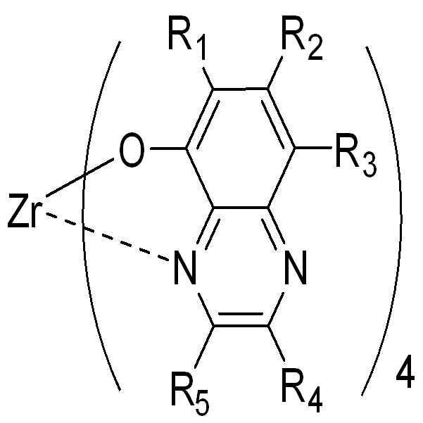
전술된 본 발명의 목적은 하기 일반식의 퀴녹살린 화합물에 의해 달성된다.The object of the present invention described above is achieved by a quinoxaline compound of the general formula:

여기서, M은 Ti, Zr, Hf, Nb, Re, Sn, 및 Ge로부터 선택된다.Here, M is selected from Ti, Zr, Hf, Nb, Re, Sn, and Ge.
각각의 R이 다른 것들과는 독립적으로 수소, C1-C20 알킬, 바람직하게는 메틸, C1-C20 알케닐, C1-C20 알키닐, 아릴, 헤테로아릴, 올리고아릴, 올리고헤테로아릴, 올리고아릴헤테로아릴, -ORx, -NRxRy, -SRx, -NO2, -CHO, -COORx, -F, -Cl, -Br, -I, -CN, -NC, -SCN, -OCN, -SORx, SO2Rx로부터 선택되거나(여기서, Rx와 Ry는 C1-C20 알킬, C1-C20 알케닐, 및 C1-C20 알키닐로부터 선택됨), 각각의 리간드의 하나 이상의 R이 축합 고리 시스템(condensed ring system)의 일부일 수 있다.Each of R and the others are independently hydrogen, C 1 -C 20 alkyl, preferably methyl, C 1 -C 20 alkenyl, C 1 -C 20 alkynyl, aryl, heteroaryl, aryl oligonucleotide, oligo-heterocyclic -OR x , -NR x R y , -SR x , -NO 2 , -CHO, -COOR x , -F, -Cl, -Br, -I, -CN, -NC, -SCN, -OCN, -SOR x , SO 2 R x wherein R x and R y are independently selected from C 1 -C 20 alkyl, C 1 -C 20 alkenyl, and C 1 -C 20 alkynyl Selected), one or more R of each ligand may be part of a condensed ring system.
각각의 리간드는 하나 이상의 치환기 R을 가질 수 있다. 상기 일반식은 각각의 퀴녹살린 리간드가 수소가 아닌 하나 이상의 치환기 R을 가질 수 있음을 의미하는 것으로 이해되어야 한다. 위에 제시된 화합물 내의 리간드의 모든 치환기 R이 수소이면, 그들은 정의에 의해 총 5개의 치환기를 갖는다.Each ligand may have one or more substituents R. It is to be understood that the above formula means that each quinoxaline ligand can have one or more substituents R, which are not hydrogen. If all the substituents R of the ligand in the above-mentioned compounds are hydrogen, they have, by definition, a total of 5 substituents.
각각의 퀴녹살린 리간드가 수소가 아닌 하나 이상의 치환기 R을 갖는 퀴녹살린이 제공되는 것이 바람직하다.It is preferred that each quinoxaline ligand is provided with quinoxaline having at least one substituent R, which is not hydrogen.
특히, R이 아릴, 헤테로아릴, 올리고아릴, 올리고헤테로아릴, 및 올리고아릴헤테로아릴로부터 선택되는 퀴녹살린 화합물이 바람직한데, 여기서 고리 결합(ring linkage)을 제공하는 역할을 하지 않는 모든 sp2 혼성 탄소 원자(sp2-hybridized carbon atom)는 서로 독립적으로 H, 메틸, C1-C20 알킬, C1-C20 알케닐, C1-C20 알키닐, -ORx, -NRxRy, -SRx, -NO2, -CHO, -COORx, -F, -Cl, -Br, -I, -CN, -NC, -SCN, -OCN, -SORx, SO2Rx로 치환될 수 있고, 여기서 Rx와 Ry는 위에서 정의된 바와 같다.In particular, R is aryl, heteroaryl, oligonucleotide aryl, oligonucleotide heteroaryl, and up aryl heteroaryl together the quinoxaline compound is selected from aryl preferably wherein the ring bond any sp 2 hybrid carbon that does not serve to provide the (ring linkage) Wherein the sp 2 -hybridized carbon atom is independently selected from H, methyl, C 1 -C 20 alkyl, C 1 -C 20 alkenyl, C 1 -C 20 alkynyl, -OR x , -NR x R y , -SR x, -NO 2, -CHO, -COOR x, -F, -Cl, -Br, -I, -CN, -NC, -SCN, -OCN, -SOR x, optionally substituted with SO 2 R x , Where R x and R y are as defined above.
본 발명의 목적은 하기 화학식들의 퀴녹살린 화합물에 의해 가장 바람직하게 달성된다.The object of the present invention is most preferably achieved by the quinoxaline compounds of the formulas:

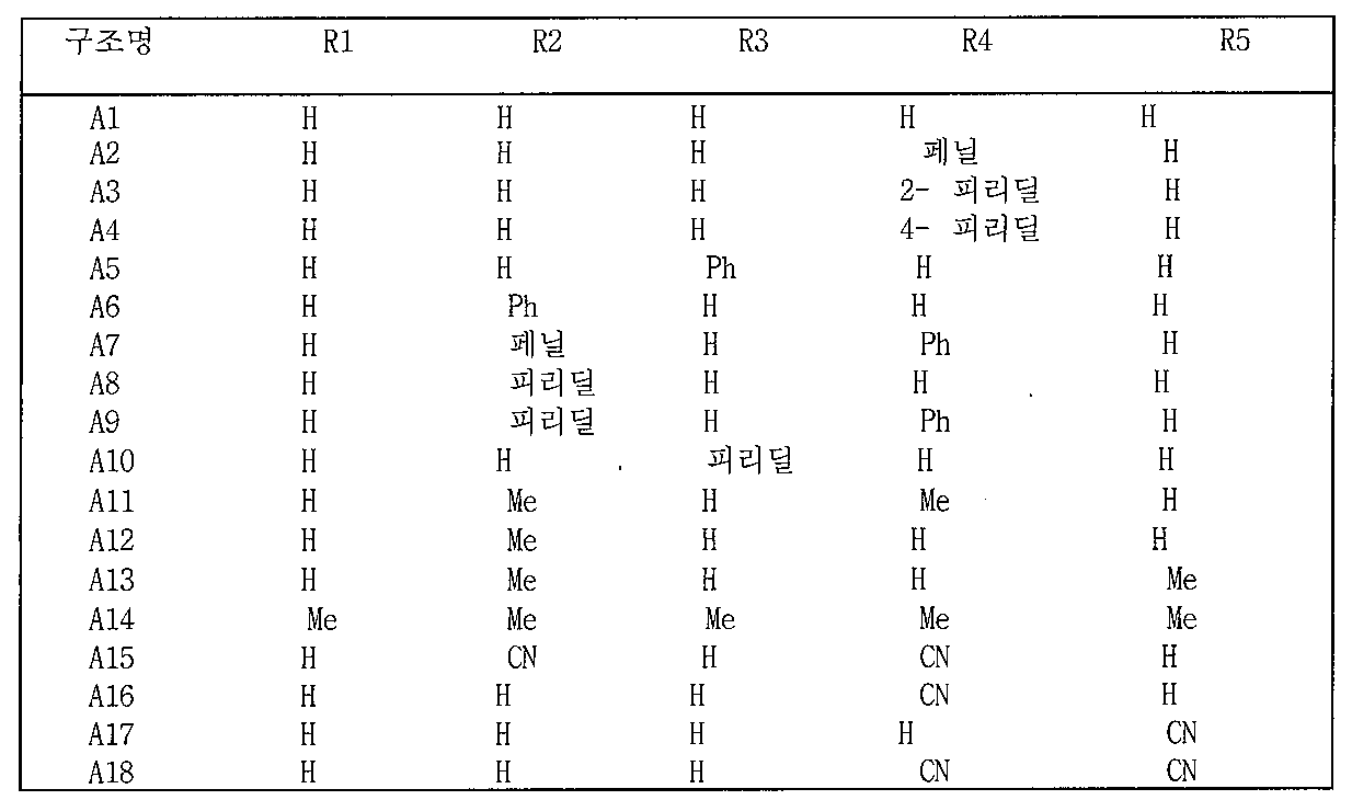
하기 치환 패턴을 갖는 퀴녹살린 화합물들도 바람직하다.Quinoxaline compounds having the following substitution patterns are also preferred.
퀴녹살린 화합물을 유기 태양 전지에서 엑시톤 블로커(exciton blocker) 또는 전자 수송 층으로서 사용하는 용도 및/또는 유기 발광 다이오드에서 전자 수송 층 또는 이미터 매트릭스(emitter matrix)로서 사용하는 용도도 또한 본 발명에 속한다.The use of the quinoxaline compound as an exciton blocker or electron transport layer in an organic solar cell and / or as an electron transport layer or an emitter matrix in an organic light emitting diode is also included in the present invention .
본 발명의 목적은 하나 이상의 도펀트로 도핑된 하나 이상의 유기 매트릭스 재료를 포함하는 유기 반도체 재료에 의해서도 또한 달성되는데, 상기 유기 매트릭스 재료는 본 발명에 따른 퀴녹살린 화합물이다.The object of the present invention is also achieved by an organic semiconductor material comprising at least one organic matrix material doped with at least one dopant, wherein the organic matrix material is a quinoxaline compound according to the invention.
본 발명의 목적을 달성하는 또 다른 접근책에 있어서, 본 발명에 따른 반도체 재료를 포함하는 유기 발광 다이오드, 유기 박막 트랜지스터, 또는 유기 태양 전지가 제공된다.In another approach for achieving the object of the present invention, there is provided an organic light emitting diode, an organic thin film transistor, or an organic solar cell including the semiconductor material according to the present invention.
퀴녹살린 화합물이 유기적으로 n-도핑되어 모든 층들의 재료가 85℃ 이상의 유리 전이 온도를 갖는 층 구조 중에 존재하는 것이 바람직하다.It is preferred that the quinoxaline compound is organically n-doped so that the material of all layers is present in the layer structure having a glass transition temperature of 85 캜 or higher.
본 발명에 따라, 유기 반도체 재료를 장기 안정성의 증대 및/또는 단락 저항의 개선을 위해 유기 발광 다이오드, 유기 박막 트랜지스터, 또는 유기 태양 전지에 사용하는 용도도 또한 본 발명에 속한다.According to the present invention, the use of an organic semiconductor material for an organic light emitting diode, an organic thin film transistor, or an organic solar battery for improving long-term stability and / or improving short-circuit resistance also belongs to the present invention.
예컨대 EP 1 804 308 또는 EP 1 808 910으로부터 공지된 바와 같이, 적층 유기 발광 다이오드들, 적층 유기 태양 전지들을 연결하기 위해 및/또는 전극과의 컨버전 컨택(conversion contact)으로서 유기 전자 소자에서의 도핑된 pn 접합이 제공될 수 있다.For example, as is known from
접합이 그 n측(n side)의 전자 수송 층에 퀴녹살린 화합물을 및/또는 p측(p side)과 n측 사이의 중간 층에 퀴녹살린 화합물을 포함하는 pn 접합도 또한 본 발명에 속한다.The present invention also relates to a pn junction comprising a quinoxaline compound in the n-side electron transport layer and / or a quinoxaline compound in the intermediate layer between the p-side and the n-side of the junction.
끝으로, 본 발명에 따른 pn 접합을 전자 소자, 광전 소자, 또는 전계 발광 소자에 사용하는 용도도 또한 제안한다.Finally, the use of a pn junction according to the present invention in an electronic device, a photoelectric device, or an electroluminescent device is also proposed.
놀랍게도, 본 발명에 따른 퀴녹살린 화합물이 특히 금속 착체 도펀트로 도핑되어 개선된 전도도를 갖는 전자 수송 재료와 같은 매트릭스 재료로서 사용될 수 있음이 판명되었다. 그러한 도핑된 층들을 사용함으로써, 본 발명에 따른 LED, 박막 트랜지스터, 및 태양 전지의 전력 효율이 증가한다. 본 발명에 따라 제안되는 퀴녹살린 화합물은 매트릭스 재료로 사용될 경우에 선행 기술에 비해 개선된 열 안정도, 감소한 구동 전압, 및 매트릭스 재료에 도입된 도펀트의 더 낮은 확산을 갖는다. 또한, 놀랍게도, -3.02 eV에서의 LUMO 위치에 의거하여 매트릭스 재료의 더욱 용이한 도핑성(dopability)이 가능함이 판명되었다. 아울러, 퀴녹살린 화합물이 저렴한 출발 재료를 기반으로 용이하게 합성될 수 있고, 조정 가능한 특성들(치환기 R의 선택에 기인한)을 가질 수 있음이 판명되었다.Surprisingly, it has been found that the quinoxaline compounds according to the present invention can be doped with metal complex dopants in particular and can be used as matrix materials such as electron transporting materials with improved conductivity. By using such doped layers, the power efficiency of LEDs, thin-film transistors, and solar cells according to the present invention is increased. The quinoxaline compounds proposed in accordance with the present invention have improved thermal stability, reduced drive voltage, and lower diffusion of dopants introduced into the matrix material when used as a matrix material than in the prior art. It has furthermore surprisingly been found that easier doping of the matrix material is possible based on the LUMO position at -3.02 eV. It has also been found that quinoxaline compounds can be easily synthesized based on inexpensive starting materials and have adjustable properties (due to the choice of substituent R).
놀랍게도, 본 발명에 따른 퀴녹살린 화합물을 포함하는 n-도핑된 층의 존재 하에 개선된 단락 저항 및/또는 증가한 장기 안정성을 갖는 소자가 얻어질 수 있음도 또한 판명되었다. 본 발명에 따른 퀴녹살린 화합물을 포함하는 투명 층으로서의 n-도핑된 층이 바람직하고, 그러한 투명 층으로서의 n-도핑된 층은 전자 소자, 광전 소자, 또는 전계 발광 소자를 제조하기 위해 온도에 따라 전자적 특성들을 변경함으로써 전류 제한 층 및/또는 단락을 방지하는 층으로서 사용될 수 있다. 그러한 투명 층의 전도도는 임계 온도 위에서 실온에서의 전도도에 비해 그 실온에서의 전도도에 대한 레벨보다 확실히 낮은 레벨로 감소하는 것으로 밝혀졌다.Surprisingly, it has also been found that devices with improved short-circuit resistance and / or increased long-term stability in the presence of an n-doped layer comprising a quinoxaline compound according to the present invention can be obtained. An n-doped layer as a transparent layer comprising a quinoxaline compound according to the present invention is preferable, and an n-doped layer as such a transparent layer is an electronically Can be used as a current confining layer and / or a layer preventing short circuit by changing properties. It has been found that the conductivity of such a transparent layer decreases to a level which is certainly lower than the level for the conductivity at room temperature compared to the conductivity at room temperature above the critical temperature.
퀴녹살린 화합물의 특히 안정적이고도 양호한 도핑성은 W(hpp)4; 4,4',5,5'-테트라시클로헥실-1,1',2,2',3,3'-헥사메틸-2,2',3,3'-테트라히드로-1H,1'H-2,2'-바이이미다졸; 2,2'-디이소프로필-1,1',3,3'-테트라메틸-2,2',3,3',4,4',5,5',6,6', 7,7'-도데카히드로-1H,1'H-2,2'-바이벤조[디]이미다졸; 2,2'-디이소프로필-4,4',5,5' -테트라키스(4-메톡시페닐)-1,1',3,3'-테트라메틸-2,2',3,3'-테트라히드로-1H,1'H-2,2'-바이이미다졸; 2,2'-디이소프로필-4,5-비스(2-메톡시페닐)-4',5'-비스(4-메톡시페닐)-1,1',3,3'-테트라메틸-2,2',3,3'-테트라히드로-1H,1'H-2,2'-바이이미다졸; 2,2'-디이소프로필-4,5-비스(2-메톡시페닐)-4',5'-비스(3-메톡시페닐)-1,1',3,3'-테트라메틸-2,2',3,3'-테트라히드로-1H,1'H-2,2'-바이이미다졸을 사용하여 달성되었다.Particularly stable and good doping properties of the quinoxaline compounds are W (hpp) 4; 4,4 ', 5,5'-tetracyclohexyl-1,1', 2,2 ', 3,3'-hexamethyl-2,2', 3,3'-tetrahydro-1H, 1'H -2,2'-biimidazole; 2,2'-diisopropyl-1,1 ', 3,3'-tetramethyl-2,2', 3,3 ', 4,4', 5,5 ', 6,6', 7,7 -Dodecahydro-1H, 1 ' H-2,2 ' -bibenzo [d] imidazole; 2,2'-diisopropyl-4,4 ', 5,5' -tetrakis (4-methoxyphenyl) -1,1 ', 3,3'-tetramethyl-2,2', 3,3 '-Tetrahydro-1H, 1'H-2,2'-biimidazole; Bis (2-methoxyphenyl) -4 ', 5'-bis (4-methoxyphenyl) -1,1', 3,3'-tetramethyl- 2,2 ', 3,3'-tetrahydro-1H, 1'H-2,2'-biimidazole; Bis (2-methoxyphenyl) -4 ', 5'-bis (3-methoxyphenyl) -1,1', 3,3'-tetramethyl- 2,2 ', 3,3'-tetrahydro-1H, 1'H-2,2'-biimidazole.
OLED에서는, pn 접합을 전하 발생 층으로 지칭하거나 연결 유닛으로까지 지칭하기도 한다.In an OLED, a pn junction may also be referred to as a charge generating layer or even as a connected unit .
유기 태양 전지에서는, pn 접합을 재결합 층으로 지칭하기도 한다.In an organic solar cell, the pn junction may be referred to as a recombination layer .
OLED 또는 태양 전지의 유기 층 배열은 전형적으로 서로 상하로 배치된 다수의 유기 층들을 포함한다. 그러한 유기 층 배열 내에는, 적층 OLED들에 대해 공지된 바와 같이(EP 1 478 0255 A2 참조), 하나 이상의 pn 접합들이 제공될 수도 있는데, 이때 그러한 pn 접합은 일 실시예에서 서로 직접 접촉한 채로 형성되는 p-도핑된 정공 수송 층과 n-도핑된 전자 수송 층에 의해 형성된다. 그러한 pn 접합은 전위를 바람직하게는 2개의 층들 사이의 경계선 영역에 인가함으로써 전하들이 발생하는 전하 발생 구조이다.The organic layer arrangement of the OLED or solar cell typically comprises a plurality of organic layers arranged one above the other. Within such an organic layer arrangement, one or more pn junctions may be provided, as is known for laminated OLEDs (see
그 pn 접합은 태양 전지 및 광센서에서는 적층 이종 접합(heterojunction)들을 결합시키고 그 소자에 의해 발생하는 전압을 부가하는데 사용된다(US 2006027834A). 그러한 접합은 비록 물리적 메커니즘이 동일한 것은 아니지만 적층 무기 이종 접합 태양 전지의 터널 접합과 동일한 기능을 갖는다.The pn junction is used to combine stacked heterojunctions in solar cells and photosensors and to add voltage generated by the device (US 2006027834A). Such a junction has the same function as the tunnel junction of a stacked inorganic heterojunction solar cell, although the physical mechanism is not the same.
그러한 접합은 전극에의 개선된 주입(태양 전지에서는 추출)을 달성하는데 사용되기도 한다(EP 1808910).Such bonding is also used to achieve improved implantation into electrodes (extraction in solar cells) (EP 1808910).
유지 전자 소자에서의 에너지 특성들을 개선하기 위해, 문헌 WO 2005/109542 A1은 n형의 유기 반도체 재료의 층이 양극으로서 구현된 전극과 접촉하도록 그 n형의 유기 반도체 재료의 층과 p형의 유기 반도체 재료의 층으로 pn 접합을 형성할 것을 제안하고 있다. 그리하여, 정공의 형태의 전하 캐리어들을 p형의 유기 반도체 재료의 층으로 주입하는 것이 개선되게 된다.In order to improve the energy characteristics in the retaining electronic device, document WO 2005/109542 A1 discloses a layer of n-type organic semiconductor material and a layer of p-type organic semiconductor material so that the layer of n- It is proposed to form a pn junction with a layer of semiconductor material. Thus, the injection of the charge carriers in the form of holes into the layer of p-type organic semiconductor material is improved.
pn 접합을 안정화시키기 위해, 다른 재료의 층이 중간 층으로서 사용될 수도 있다. 그와 같이 안정화되는 pn 접합은 예컨대 US 2006040132A에 개시되어 있는데, 여기서는 금속이 중간 층으로서 사용된다. 그러한 금속 층을 갖는 OLED는 금속 이온들의 확산으로 인해 더 짧은 수명을 갖는다.To stabilize the pn junction, a layer of another material may be used as the intermediate layer. Such stabilized pn junction is disclosed, for example, in US 2006040132A, wherein a metal is used as the intermediate layer. OLEDs with such metal layers have a shorter lifetime due to diffusion of metal ions.
안정된 유기 반도체 소자를 제조하기 위해, 본 발명에 따른 퀴녹살린 화합물을 포함하는 pn 접합들 사이에 안정된 중간 층 및/또는 도핑된 중간 층이 제공될 수도 있다.In order to produce a stable organic semiconductor device, a stable intermediate layer and / or a doped intermediate layer may be provided between the pn junctions comprising the quinoxaline compound according to the present invention.
그러한 pn 접합은 양 재료들이 모두 p형과 n형으로 도핑될 경우에 매우 효율적으로 작용하는 것이 공지되어 있다(EP 1804308, EP 1804309).Such a pn junction is known to work very efficiently when both materials are doped both p-type and n-type (EP 1804308, EP 1804309).
효율적이고 안정된, 주로 열적으로 안정된 pn 접합을 제공하는 재료 및 재료 조합을 생성하는 것도 가능하다.It is also possible to produce materials and material combinations that provide efficient and stable, primarily thermally stable pn junctions.
놀랍게도, 본 발명에 따른 퀴녹살린 화합물은 단락 저항을 갖는 안정적인 도핑된 층들을 형성하는 것으로 판명되었다. 바람직하게는, 유기 도펀트로 도핑되고 본 발명에 따른 퀴녹살린 화합물을 함유하는(바람직하게는 55 mol%를 넘는 함량으로) 층이 유기 전자 소자, 광전 소자, 및 전계 발광 소자에서 그 소자들이 단락에 저항성을 갖도록 전자 수송 층으로 사용될 수 있다.Surprisingly, it has been found that the quinoxaline compounds according to the present invention form stable doped layers with short-circuit resistance. Preferably, a layer doped with an organic dopant and containing a quinoxaline compound according to the present invention (preferably in an amount greater than 55 mol%) is used in organic electronic devices, optoelectronic devices, and electroluminescent devices, It can be used as an electron transporting layer to have resistance.
본 발명의 추가의 특징들 및 이점들은 바람직한 예시적 실시예에 관한 이후의 상세한 설명으로부터 도출될 것이다.Further features and advantages of the present invention will be derived from the following detailed description of the preferred exemplary embodiments.
ZrZr 테트라퀴녹살린Tetraquinoxaline 착체의Complex 제조 Produce
예 AExample A
리간드 5-히드록시퀴녹살린을 3B Scientific Corporation으로부터 상업적으로 수득하였다.The ligand 5-hydroxyquinoxaline was obtained commercially from 3B Scientific Corporation.
US 7,230,107 B1으로부터의 합성 절차에 따라, 사염화지르코늄 0.23g을 메탄올 10mL 중에 용해시킨 후에 5-히드록시퀴녹살린 0.86g에 첨가하고, 아울러 글러브박스에서 메탄올 10mL 중에 교반하면서 용해시켰다. 이어서, 트리에틸아민 0.45g을 한 방울씩 첨가하였다. 그 혼합물을 글러브박스에서 15분 동안 실온 교반하였다. 그러자, 결정질 고형물이 서서히 침전하기 시작하였다. 여과에 의해 그 고형물을 회수하고, 다시 염화메틸렌 중에 용해시켜 여과하고 진공 중에서 건조될 때까지 증발시켰다. 결과적으로 얻은 고형물을 사용 전에 승화에 의해 정제하였다.According to the synthetic procedure from US 7,230,107 B1, 0.23 g of zirconium tetrachloride was dissolved in 10 mL of methanol and then added to 0.86 g of 5-hydroxyquinoxaline and dissolved in 10 mL of methanol in a glove box with stirring. Then 0.45 g of triethylamine was added dropwise. The mixture was stirred in a glovebox for 15 minutes at room temperature. The crystalline solid began to precipitate slowly. The solid was recovered by filtration, dissolved again in methylene chloride, filtered and evaporated to dryness in vacuo. The resulting solids were purified by sublimation prior to use.
본 명세서의 서론에서 설명된 방법들에 따라, 본 발명에 따른 Zr 테트라퀴녹살린 착체의 전도도 및 열 안정도를 결정하였다. 여기에서 설명된 실시예에서 제조된 착체를 10 mol%의 도펀트(화합물 Ia)로 도핑하였다. 실온에서의 전도도는 1.9×10⁻⁵S/cm이었다. 열 안정도는 121℃이었다.The conductivity and thermal stability of the Zr tetraquinoxaline complexes according to the present invention were determined according to the methods described in the introduction of the present specification. The complexes prepared in the examples described herein were doped with 10 mol% of a dopant (compound Ia). The conductivity at room temperature was 1.9 × 10 -5 S / cm. The thermal stability was 121 占 폚.
비교를 위해, 4-(나프탈렌-1-일)-2,7,9-트리페닐-피리도[3.2-h]퀴나졸린으로 유사한 시험을 수행하였다. 이때의 전도도는 7.3×10⁻⁶S/cm에 불과하였던 한편, 열 안정도는 87℃이었다.For comparison, a similar test was performed with 4- (naphthalen-1-yl) -2,7,9-triphenyl-pyrido [3.2-h] quinazoline. The conductivity at this time was only 7.3 × 10 -6 S / cm, while the thermal stability was 87 ° C.
마찬가지로, 본 발명에 따른 구조에 있어서는 구동 전압(1000cd/m2에서의)이 2.13 V이었던 반면, 4-(나프탈렌-1-일)-2,7,9-트리페닐-피리도[3.2h]퀴나졸린에 있어서는 2.45 V의 구동 전압이 얻어졌다. 85℃에서, 본 발명에 따른 매트릭스 재료에서는 도펀트의 확산이 발견되지 않았던 반면, 4-(나프탈렌-1-일)-2,7,9-트리페닐-피리도[3.2h]퀴나졸린을 사용한 경우에는 도펀트의 확산이 3nm에 달하였다.Likewise, in the structure according to the present invention, the driving voltage (at 1000 cd / m 2 ) was 2.13 V, while 4- (naphthalene-1-yl) -2,7,9-triphenyl- And a driving voltage of 2.45 V was obtained for quinazoline. At 85 캜, no diffusion of the dopant was found in the matrix material according to the invention, whereas when 4- (naphthalen-1-yl) -2,7,9-triphenyl-pyrido [3.2h] quinazoline was used The diffusion of the dopant reached 3 nm.
예 BExample B
하기 화합물을 합성하였다.The following compounds were synthesized.
리간드 페나진-1-올을 VWR로부터 상업적으로 수득하였다.The ligand phenazin-1-ol was obtained commercially from VWR.
US 7,230,107 B1으로부터의 합성 절차에 따라, 사염화지르코늄 0.23g을 글러브박스에서 메탄올 10mL 중에 용해시킨 후에 페나진-1-올 0.86g에 첨가하고, 아울러 메탄올 10mL 중에 교반하면서 용해시켰다. 다음으로, 트리에틸아민 0.45g을 한 방울씩 첨가하였다. 그 혼합물을 글러브박스에서 15분 동안 실온 교반하였다. 그러자, 결정질 고형물이 서서히 침전하여 석출되기 시작하였다. 여과에 의해 그 고형물을 회수하고, 다시 염화메틸렌 중에 용해시켜 여과하고 진공 중에서 건조될 때까지 증발시켰다. 결과적으로 얻은 고형물을 사용 전에 승화에 의해 정제하였다.According to the synthetic procedure from US 7,230,107 B1, 0.23 g of zirconium tetrachloride was dissolved in 10 ml of methanol in a glove box and then added to 0.86 g of phenazin-1-ol and dissolved in 10 ml of methanol with stirring. Next, 0.45 g of triethylamine was added dropwise. The mixture was stirred in a glovebox for 15 minutes at room temperature. The crystalline solid then precipitated slowly and began to precipitate. The solid was recovered by filtration, dissolved again in methylene chloride, filtered and evaporated to dryness in vacuo. The resulting solids were purified by sublimation prior to use.
예 CYes C
하기 화합물을 합성하였다.The following compounds were synthesized.

리간드 2,3-디메틸퀴녹살린-5-올을 Hanzhou Chempro로부터 상업적으로 수득하였다.The
US 7,230,107 B1으로부터의 합성 절차에 따라, 사염화지르코늄 0.8g을 글러브박스에서 메탄올 80mL 중에 용해시킨 후에 2,3-디메틸퀴녹살린-5-올 2.4g에 첨가하고, 아울러 메탄올 20mL 중에 교반하면서 용해시켰다. 이어서, 피페리딘 2mL를 한 방울씩 첨가하였다. 그 혼합물을 글러브박스에서 2시간 동안 실온 교반하였다. 그러자, 황색 결정질 고형물이 서서히 침전하기 시작하였다. 여과에 의해 그 고형물을 회수하고, 진공 중에서 건조될 때까지 증발시켰다. 결과적으로 얻은 고형물을 사용 전에 승화에 의해 정제하였고 수율은 78%(1.99g)이었다.According to the synthetic procedure from US 7,230,107 B1 0.8 g of zirconium tetrachloride was dissolved in 80 mL of methanol in a glove box and added to 2.4 g of 2,3-dimethylquinoxalin-5-ol and dissolved in 20 mL of methanol with stirring. Then, 2 mL of piperidine was added dropwise. The mixture was stirred in a glovebox for 2 hours at room temperature. The yellow crystalline solid began to precipitate slowly. The solid was collected by filtration and evaporated to dryness in vacuo. The resulting solids were purified by sublimation prior to use and the yield was 78% (1.99 g).
본 발명에 따른 퀴녹살린 화합물의 추가의 특징들 및 이점들은 물론 그 용도, 예컨대 유기 발광 다이오드에 사용하는 용도도 첨부 도면들에 의거한 이후의 예시적 실시예들에 대한 상세한 설명으로부터 도출될 것이다. 첨부 도면들 중에서,
도 1은 전형적 OLED 구조의 단면도이고;
도 2는 전형적 태양 전지의 단면도이며;
도 3은 2개의 OLED들의 작동 전압에 대한 광도의 의존성을 나타낸 그래프이고;
도 4는 85℃에서의 저장 시간에 따른 1000cd/m2에서의 작동 전압을 나타낸 그래프이며;
도 5는 전압에 따른 전류 밀도를 나타낸 그래프이고;
도 6은 시간에 따른 전압을 나타낸 그래프이다.The additional features and advantages of the quinoxaline compounds according to the present invention will of course be derived from the detailed description of the following illustrative embodiments, as well as their use in organic light emitting diodes, for example, with reference to the accompanying drawings. In the accompanying drawings,
1 is a cross-sectional view of a typical OLED structure;
2 is a cross-sectional view of a typical solar cell;
3 is a graph showing the dependence of luminous intensity on the operating voltage of two OLEDs;
4 is a graph showing the operating voltage at 1000 cd / m < 2 > with storage time at 85 [deg.] C;
5 is a graph showing a current density according to a voltage;
6 is a graph showing the voltage with time.
본 발명에 따라 제안되는 화합물은 효율적인 OLED를 제조하는데 특히 적합하다.The compounds proposed according to the invention are particularly suitable for the production of efficient OLEDs.
도 1은 OLED의 전형적 층 구조를 단면도로 나타낸 것이다. 층들은 다음의 순서로 기판(10) 상에 부착된다: 양극(11), p-도핑된 정공 수송 층(12), 전자 블로커(13), 발광 층(14), 정공 블로커(15), n-도핑된 전자 수송 층(16), 및 음극(17). 조합된 특성들이 있으려면 2개 이상의 층들을 조합할 수 있다. 도 1에 도시된 구조 이외에, 당업자라면 역전(inverted) 층 구조, 전면 발광(top-emitting) OLED, 투명 OLED, 및 적층 OLED도 잘 알고 있을 것이다. 이미터 층은 통상적으로 이미터 매트릭스와 이미터 염료(이미터 도펀트)로 이뤄진다. 그러나 그러한 이미터 층은 다수의 층들 및 상이한 재료들의 조합일 수도 있다.Figure 1 shows a cross-sectional view of a typical layer structure of an OLED. The layers are deposited on the
본 발명에 따른 화합물은 유기 태양 전지를 제조하는데에도 역시 적합하다.The compounds according to the invention are also suitable for the production of organic solar cells.
도 2는 유기 태양 전지의 전형적 층 구조를 단면도로 나타낸 것이다. 층들은 다음의 순서로 기판(20) 상에 부착된다: 양극(21), p-도핑된 정공 수송 층(22), 광활성적(photoactive)일 수도 있는 도핑되지 않은 정공 수송 층(23), 광활성 층(24), 광활성적일 수도 있는 전자 수송 층(25), n-도핑된 전자 수송 층(26), 및 음극(27). 유기 태양 전지에 대한 추가의 층 구조들도 역시 당업자에게는 익숙할 것이다. 예컨대, n-도핑된 전자 수송 층(26) 대신에, 얇은 버퍼 층(buffer layer)이 사용될 수 있다. 조합된 특성들이 있으려면 바로 2개 이상의 층들을 조합할 수 있다.2 is a cross-sectional view of a typical layer structure of an organic solar cell. The layers are deposited on the
유기 발광 다이오드의 제조Manufacture of organic light-emitting diodes
실시예Example 1 One
예 A에 따른 지르코늄 테트라퀴녹살린 착체를 사용하여 OLED를 제조하였다. ITO(산화인듐아연)(ITO 층 두께는 90nm)로 코팅된 유리 기판을 초음파 욕 중에서 에탄올, 아세톤, 및 이소프로판올로 각각 5분 동안 씻어내었다. 이어서, 기판을 오존 플라즈마 중에서 5분 동안 정화한 다음 진공 중으로 옮겼다. 높은 진공 하에서, 새도 마스크를 사용하여 ITO 표면이 추후의 전기 접촉을 위해 개방된 채 유지되도록 유기 층들 및 전극을 기판 상에 증착하였다. 열 진공 증착에 의해, ITO 층상에 n-도핑된 정공 수송 층을 증착하였다(4,4',4"-(1E,1'E,1"E)-시클로프로판-1,2,3-트리일리덴트리스(시아노-메탄-1-일-1-일리덴)트리스(2,3,5,6-테트라플루오로벤조니트릴), 3 wt%로 도핑된 60nm NPD-N,N'-디페닐-N,N'-비스(1-나프틸)-1,1'-바이페닐-4,4"-디아민). p-도핑된 정공 수송 층 상에 10 nm NPD 층을 증착하였다. 그 뒤를 이어 상업 적색 염료(10 wt%)로 도핑된 20nm 두께의 루브렌(rubrene) 이미터 층을 증착하였다. DCJTB(4-(디시아노메틸렌)-2-3차-부틸-6-(1,1,7,7-테트라메틸쥬롤이딜-9-엔일)-4H-피란)을 적색 이미터로서 사용할 수도 있다. 이미터 층 상에 Zr 퀴녹살린 화합물의 10nm 두께의 층을 증착하였다. 그 뒤를 이어 테트라키스(1,3,4,6,7,8-헥사히드로-2H-피리미도-[1.2-a]피리미디나토)디텅스텐(Ⅱ)(W(hpp)4)(10 wt%)로 도핑된 지르코늄 테트라퀴녹살린 착체의 60nm 두께의 층을 증착하였다. 끝으로, 100nm 두께의 알루미늄 층을 음극으로서 증착하였다. 본 실시예의 결과, 1000cd/m2에서 2.15 V의 구동 전압이 나왔다.The zirconium tetraquinoxaline complex according to Example A was used to prepare an OLED. The glass substrate coated with ITO (indium zinc oxide) (ITO layer thickness: 90 nm) was rinsed with ethanol, acetone, and isopropanol in an ultrasonic bath for 5 minutes each. Subsequently, the substrate was cleaned in an ozone plasma for 5 minutes and then transferred into a vacuum. Under high vacuum, organic layers and electrodes were deposited on the substrate using a trench mask so that the ITO surface remains open for future electrical contact. A n-doped hole transport layer was deposited on the ITO layer by thermal vacuum deposition (4,4 ', 4 "- (1E, 1'E, 1" E) -cyclopropane- N, N'-di (triphenylphosphine) doped with 3 wt% of bis (diphenylphosphino) Phenyl-N, N'-bis (1-naphthyl) -1,1'-biphenyl-4,4'-diamine). A 10 nm NPD layer was deposited on the p-doped hole transport layer. A 20 nm thick rubrene emitter layer doped with commercial red dye (10 wt%) was then deposited. DCJTB (4- (dicyanomethylene) -2,3-tert-butyl-6- (1,1 , 7,7-tetramethyluronyldil-9-enyl) -4H-pyran) can also be used as the red emitter. A 10 nm thick layer of the Zr quinoxaline compound is deposited on the emitter layer. a - ([1.2-a] pyrimidinyl
비교예Comparative Example 2 2
전술된 실시예 1에서 설명된 바와 같이 유기 발광 다이오드를 제조하되, 다만 지르코늄 테트라퀴녹살린 착체를 4-(나프탈렌-1-일)-2,7,9-트리페닐-피리도[3.2-h]퀴나졸린으로 대체하였다. 본 비교예의 결과, 1000cd/m2에서 2.45 V의 작동 전압이 나왔다.(Naphthalen-1-yl) -2,7,9-triphenyl-pyrido [3.2-h] pyrimidin- Quinazoline. ≪ / RTI > As a result of this comparative example, an operating voltage of 2.45 V was obtained at 1000 cd / m 2 .
도 3은 제조된 상기 2개의 OLED들의 광도를 작동 전압에 따라 나타낸 것이다. 속이 빈 원들은 선행 기술의 화합물을 포함한 OLED에 대한 측정 데이터를 나타내는 반면, 속이 채워진 원들은 본 발명에 따른 화합물을 사용하여 제조된 OLED에 의거한 것이다.3 shows the luminances of the two OLEDs manufactured according to the operating voltage. Hollow circles represent measurement data for OLEDs containing prior art compounds while hollow filled circles are based on OLEDs made using compounds according to the present invention.
도 4는 1000cd/m2에서의 작동 전압을 85℃에서의 저장 시간에 따라 나타낸 것이다. 선행 기술의 화합물을 포함한 OLED가 속이 빈 사각형들에 따른 곡선으로 표시되어 본 발명에 따른 화합물을 사용한 OLED(속이 채워진 사각형들에 따른 곡선)와 비교되어 있다. 본 발명에 따른 OLED는 약 2.15 V의 낮은 작동 전압을 갖는 이외에 높은 열 안정도도 갖는데, 작동 전압은 1000시간 후에도 거의 변하지 않는다. 같은 시간에, 선행 기술의 화합물을 포함한 OLED의 작동 전압은 약 2.4 V로부터 2.7 V로 증가하였다.Figure 4 shows the operating voltage at 1000 cd / m < 2 > according to the storage time at 85 [deg.] C. OLEDs containing compounds of the prior art are compared to OLEDs (curves according to hollow filled squares) using compounds according to the present invention as indicated by curves along hollow squares. The OLED according to the present invention has a high thermal stability in addition to having a low operating voltage of about 2.15 V, and the operating voltage hardly changes after 1000 hours. At the same time, the operating voltage of OLEDs containing prior art compounds increased from about 2.4 V to 2.7 V,
본 실시예들에 한정되지 않는 전력 효율 및 수명과 같은 특히 양호한 특성들이 다음의 p 도펀트들을 사용한 p-도핑에 의해 달성되었다: 2,2'-(퍼플루오로나프탈렌-2,6-디일리덴)디말로노니트릴; 2,2'-(2,5-디브로모-3,6-디플루오로시클로헥사-2,5-디엔-1,4-디일리덴)디말로노니트릴; (2E,2'E,2"E)-2,2',2"-(시클로프로판-1,2,3-트리일리덴)트리스(2-(2,6-디클로로-3,5-디플루오로-4-(트리플루오로메틸)페닐)아세토니트릴); 4,4',4"-(1E,1'E,1"E)-시클로프로판-1,2,3-트리일리덴트리스(시아노메탄-1-일-1-일리덴)-트리스(2,3,5,6-테트라플루오로벤조니트릴).Particularly good properties such as power efficiency and lifetime not limited to these embodiments have been achieved by p-doping using the following p dopants: 2,2 '- (perfluoronaphthalene-2,6-diylidene ) Dimalononitrile; 2,2 '- (2,5-dibromo-3,6-difluorocyclohexa-2,5-diene-1,4-diylidene) dimalononitrile; (2E, 2'E, 2 "E) -2,2 ', 2" - (cyclopropane-1,2,3-triylidene) tris (2- (2,6- Fluoro-4- (trifluoromethyl) phenyl) acetonitrile); 4,4 ', 4 "- (1E, 1'E, 1" E) -cyclopropane-1,2,3-triylidene tris (cyanomethan-1-yl-1-ylidene) -
실시예Example 3: 지르코늄 3: zirconium 테트라퀴녹살린Tetraquinoxaline 착체를Complex 포함한 유기 태양 전지 Organic solar cell including
종래의 CuPc-C60 태양 전지("벌크 이종 접합")를 다음과 같이 제조하였다: 예 A에따른 전술된 지르코늄 테트라퀴녹살린을 사용하여 OLED를 제조하였다. ITO(ITO 층 두께는 90nm)로 코팅된 유리 기판을 초음파 욕 중에서 에탄올, 아세톤, 및 이소프로판올로 각각 5분 동안 세정하였다. 이어서, 기판을 오존 플라즈마 중에서 5분 동안 세정한 다음 진공 중으로 옮겼다. 높은 진공(10-3Pa 미만의 압력) 하에서, 열 진공 증착에 의해 다음의 순서로 층들을 부착하였다: F4-TCNQ(5 wt%)로 도핑된 10nm 두께의 CuPc; 10nm 두께의 도핑되지 않은 CuPc(구리 프탈로시아닌); 30nm 두께의 C60 중 CuPc의 1:2(w/w) 혼합물; 40nm 두께의 도핑되지 않은 C60 층; 10nm 두께의 지르코늄 테트라퀴녹살린의 층; 100nm 두께의 알루미늄 음극. 알루미늄의 증착을 위한 증착실 내의 압력은 유기 층들의 증착을 위한 압력보다 약간 더 높았으나, 여전히 10-2Pa 미만이었다.A conventional CuPc-C60 solar cell ("bulk heterojunction") was prepared as follows: OLEDs were prepared using the zirconium tetraquinoxaline described above according to Example A. The glass substrate coated with ITO (ITO layer thickness: 90 nm) was cleaned with ethanol, acetone, and isopropanol in an ultrasonic bath for 5 minutes each. Subsequently, the substrate was cleaned in an ozone plasma for 5 minutes and then transferred into a vacuum. Under high vacuum (pressure less than 10 < -3 > Pa) the layers were deposited by thermal vacuum deposition in the following order: 10 nm thick CuPc doped with F4-TCNQ (5 wt%); 10 nm thick undoped CuPc (copper phthalocyanine); 1: 2 (w / w) mixture of CuPc in C60 of 30 nm thickness; An undoped C60 layer 40 nm thick; A 10 nm thick zirconium tetraquinoxaline layer; 100 nm thick aluminum cathode. The pressure in the deposition chamber for the deposition of aluminum was slightly higher than the pressure for deposition of the organic layers, but still less than 10 < -2 & gt ; Pa.
실시예Example 4: 4: BCPBCP 를 포함한 유기 태양 전지Organic solar cells
실시예 3에서 설명된 바와 같이 유기 태양 전지를 제조하되, 다만 지르코늄 테트라퀴녹살린 착체 대신에 10nm 층 두께의 바소큐프로인(bathocuproin; BCP)를 사용하였다.An organic solar cell was prepared as described in Example 3 except that 10 cm thick bathocuproin (BCP) was used instead of zirconium tetraquinoxaline complex.
상기 2개의 유기 태양 전지들의 AM 1.5(air mass 1.5)로 시뮬레이션된 태양 스펙트럼 하에서의 광전 특성들은 유사하다. 실시예 4의 유기 태양 전지는 Voc = 0.51 V, FF = 43%, Isc = 8.13mA/cm2를 갖는 반면, 실시예 3의 유기 태양 전지는 Voc = 0.50 V, FF = 41%, Isc = 7.99mA/cm2를 갖는다.The photoelectric properties under simulated solar spectra with the AM 1.5 (air mass 1.5) of the two organic solar cells are similar. The organic solar cell of Example 4 had V oc = 0.51 V, FF = 43% and Isc = 8.13 mA / cm 2 while the organic solar cell of Example 3 had V oc = 0.50 V, FF = 41%, Isc = 7.99 mA / cm < 2 & gt ;.
양 태양 전지들에 열 하중을 걸었다. IV 특성 곡선을 측정하고, 이어서 태양 전지의 온도를 1℃씩 증가시키면서 그때마다 10분 동안 대기하였다. 상기 절차를 반복하였다(측정, 가열, 대기). 실시예 4의 소자는 67℃에서 더 이상 제 기능을 하지 못하였다(FF = 25%, Isc < 1mA/cm2). 실시예 3의 소자는 85℃까지 IV 특성 곡선에서의 어떠한 큰 변화도 없이 여전히 제 기능을 하고 있었고, 그 후에 측정을 종료하였다.Both solar cells were subjected to thermal loads. IV characteristic curves were measured, and then the temperature of the solar cell was increased by 1 DEG C and each time, it was waited for 10 minutes. The procedure was repeated (measurement, heating, atmospheric). The device of Example 4 no longer functions at 67 캜 (FF = 25%, Isc <1 mA / cm 2 ). The device of Example 3 was still functioning without any significant change in the IV characteristic curve up to 85 DEG C, after which the measurement was terminated.
실시예Example 5: 5: pnpn 접합의 제조 Manufacturing of joints
안정된 pn 접합을 갖는 소자를 ITO 양극 상에 다음과 같이 제조하였다:A device with stable pn junction was fabricated on an ITO anode as follows:
a) p형으로 도핑된 정공 수송 층으로서의, 2-(6-디시아노-메틸렌-1,3,4,5,7,8,-헥사플루오로-6H-나프탈렌-2-일리덴)말로노니트릴 4 mol%로 도핑된 50nm의 2,2',7,7'-테트라키스-(N,N-디메틸페닐아미노)-9,9'-스피로바이플루오렌;a) doping the hole transport layer with a dopant selected from the group consisting of 2- (6-dicyano-methylene-1,3,4,5,7,8, -hexafluoro-6H-naphthalen- 50 nm of 2,2 ', 7,7'-tetrakis- (N, N-dimethylphenylamino) -9,9'-spirobifluorene doped with 4 mol% of nitrile;
b) 중간 층으로서의 10nm의 NPB;b) 10 nm NPB as an intermediate layer;
c) 20nm의 스피로-DPVBI;c) Spiro-DPVBI at 20 nm;
d) 10nm의 2,4,7,9-테트라페닐-1,10-페난트롤린;d) 2,4,7,9-tetraphenyl-1,10-phenanthroline of 10 nm;
e) n형으로 도핑된 전자 수송 층으로서의, NDOP 5 mol%로 도핑된 45nm의 예 A에 따른 지르코늄 테트라퀴녹살린 착체;e) 45 nm of a zirconium tetraquinoxaline complex according to Example A doped with 5 mol% of NDOP as an n-type doped electron transport layer;
f) p형으로 도핑된 정공 수송 층으로서의, 2-(6-디시아노-메틸렌-1,3,4,5,7,8-헥사플루오로-6H-나프탈렌-2-일리덴)말로노니트릴 4 mol%로 도핑된 50nm의 2,2',7,7'-테트라키스-(N,N-디메틸페닐아미노)-9,9'-스피로바이플루오렌;f) 2- (6-dicyano-methylene-1,3,4,5,7,8-hexafluoro-6H-naphthalen-2-ylidene) malononitrile as a p-type doped hole transport layer 50 nm of 2,2 ', 7,7'-tetrakis- (N, N-dimethylphenylamino) -9,9'-spirobifluorene doped with 4 mol%;
g) 중간 층으로서의 10 nm의 NPB;g) 10 nm NPB as an intermediate layer;
h) 20nm의 스피로-DPVBI;h) Spiro-DPVBI of 20 nm;
i) 10nm의 2,4,7,9-테트라페닐-1,10-페난트롤린;i) 2,4,7,9-tetraphenyl-1,10-phenanthroline of 10 nm;
j) n형으로 도핑된 전자 수송 층으로서의, NDOP 5 mol%로 도핑된 20nm의 2,4,7,9-테트라페닐-1,10-페난트롤린;j) 20
k) 반사 전극(mirror electrode)으로서의 100nm의 알루미늄.k) 100 nm aluminum as a mirror electrode.
결과물은 도핑된 수송 층들에 분자 도펀트들을 사용한 청색의 적층 PIN-OLED이었는데, 여기서 f) 및 g) 층들이 도핑된 pn 접합에 해당한다.The result was a blue laminated PIN-OLED using molecular dopants in doped transport layers, where f) and g) layers correspond to a doped pn junction.
본 소자는 8.9 V에서 10.8cd/A의 전류 효율로 1000cd/cm2의 광도를 발생하였다.The device produced a luminous efficiency of 1000 cd / cm 2 at a current efficiency of 10.8 cd / A at 8.9 V.
실시예Example 6: 6: pnpn 접합의 제조 Manufacturing of joints
안정된 pn 접합을 시험하기 위한 소자를 ITO 양극 상에 다음과 같이 제조하였다:A device for testing a stable pn junction was prepared on an ITO anode as follows:
a) HBL(hole blocker layer; 정공 블로커 층)로서의 50nm의 예 A에 따른 지르코늄 테트라퀴녹살린 착체;a) a zirconium tetraquinoxaline complex according to Example A of 50 nm as HBL (hole blocker layer);
b) n형으로 도핑된 전자 수송 층으로서의, NDOP 5 mol%로 도핑된 50nm의 예 A에 따른 지르코늄 테트라퀴녹살린 착체;b) 50 nm of a zirconium tetraquinoxaline complex according to Example A doped with 5 mol% of NDOP as an n-type doped electron transport layer;
c) 도핑되지 않은 중간 층으로서의 5nm의 CuPc;c) 5 nm CuPc as an undoped intermediate layer;
d) 2-(6-디시아노메틸렌-1,3,4,5,7,8-헥사플루오로-6H-나프탈렌-2-일리덴)말로노니트릴로 도핑된 50nm의 a-NPD;d) 2- (6-dicyanomethylene-1,3,4,5,7,8-hexafluoro-6H-naphthalen-2-ylidene) malononitrile doped 50 nm a-NPD;
e) 음극으로서의 100 nm의 Al.e) 100 nm of Al as the cathode.
HBL과 EBL(electron blocker layer; 전자 블로커 층)로 인해, 정공들 또는 전자들이 순방향으로 주입될 수 없다(도 5 참조, 네거티브 전압들, 양극은 포지티브). 역방향으로는, pn 접합에서 전하 캐리어들이 발생한다(도 5 참조, 포지티브 전압들, 양극은 네거티브). 도 5는 본 구조의 특성 곡선(전류 밀도 대 전압)을 나타낸 것이다.Due to HBL and EBL (electron blocker layer), holes or electrons can not be injected in the forward direction (see FIG. 5, negative voltages, positive is positive). In the reverse direction, charge carriers are generated at the pn junction (see FIG. 5, positive voltages, positive polarity). Fig. 5 shows the characteristic curve (current density vs. voltage) of this structure.
실시예Example 7: 7: pnpn 접합의 안정성 비교 Stability comparison of bonding
pn 접합들의 안정성을 조사하기 위해 다음의 표본들을 제조하였다:To investigate the stability of pn junctions, the following samples were prepared:

"p:"는 4,4',4"-시클로프로판-1,2,3-트리일리덴트리스(시아노메탄-1-일-1-일리덴)트리스(2,3,5,6-테트라플루오로벤조니트릴) 3 mol%로 p-도핑한 것을 나타낸다.quot; p: "refers to 4,4 ', 4" -cyclopropane-1,2,3-triylidene tris (cyanomethan-1-yl-1-ylidene) tris (2,3,5,6- Doped with 3 mol% of tetrafluorobenzonitrile).
도 6은 pn 접합들에 걸친 전압을 나타낸 것이다. 각각의 pn 접합은 40mA/cm2에서 작동하고, 전하 캐리어들이 pn 접합에서 발생하도록 분극된다. 그 결과는 pn 접합들이 낮은 전압을 갖고, Alq3에서보다는 중간 층을 갖거나 갖지 않는 예 A에서 훨씬 더 안정적임을 보여주고 있다. 6.3 및 6.4 곡선들은 거의 700시간에 달하는 전체 측정 시간에 걸쳐 변화가 거의 없음을 보여주고 있다.Figure 6 shows the voltage across the pn junctions. Each pn junction operates at 40 mA / cm < 2 > and the charge carriers are polarized to occur at the pn junction. The results show that the pn junctions are much more stable in Example A with low voltage and with or without an intermediate layer than in Alq3. The 6.3 and 6.4 curves show little change over the entire measuring time of almost 700 hours.
실시예Example 8: 8: OLEDOLED
예 C의 화합물로(예 A 대신에) 실시예 1을 반복하였고, 그 결과 1000cd/m2에서 2.10 V의 구동 전압이 나왔다.Example 1 was repeated with the compound of Example C (instead of Example A), resulting in a driving voltage of 2.10 V at 1000 cd / m 2 .
실시예Example 9: 9: pnpn 접합의 제조 Manufacturing of joints
예 C의 화합물로(예 A 대신에) 실시예 5를 반복하였고, 그 결과 8.8 V에서 1000cd /m2의 광도가 나왔다.Example 5 was repeated with the compound of Example C (instead of Example A), resulting in a luminance of 1000 cd / m 2 at 8.8 V.
실시예Example 10: 10: pnpn 접합의 제조 Manufacturing of joints
예 B의 화합물로(예 A 대신에) 실시예 5를 반복하였고, 그 결과 9.5 V에서 1000cd /m2의 광도가 나왔다.Example 5 was repeated with the compound of Example B (instead of Example A), resulting in a luminance of 1000 cd / m 2 at 9.5 V.
실시예Example 11: 11: OLEDOLED 의 제조Manufacturing
50nm×50nm의 크기를 갖는 10개의 OLED들을 실시예 1에 따라 제조하였다. 50nm×50nm의 크기를 갖는 추가의 10개의 OLED들을 실시예 1에 따라, 그러나 Zr 퀴녹살린 화합물을 2,4,7,9-테트라페닐-1,10-페난트롤린으로 대체하여 대조군으로서 제조하였다.Ten OLEDs with a size of 50 nm x 50 nm were prepared according to Example 1. A further 10 OLEDs with a size of 50 nm x 50 nm were prepared according to Example 1, but replacing the Zr quinoxaline compound with 2,4,7,9-tetraphenyl-1,10-phenanthroline as a control .
수율은 100%로서, 20개의 OLED들 모두 기능적이고 결함이 없었다.The yield was 100%, and all 20 OLEDs were functional and defect free.
샘플들을 4000cd/m2에서 500시간 동안 노화시켰다. 불과 100시간 후, 대조군 OLED들 중의 3개가 작은 가시적 결함들을 가졌다. 500시간 후, 대조군 OLED들 중의 5개가 OLED 표면에 걸쳐 퍼져나간 결함들을 가졌고, 2개가 완파되었다. Zr 퀴녹살린 화합물을 포함한 샘플들은 500시간 후 어떠한 결함도 갖지 않았다.The samples were aged at 4000 cd / m < 2 > for 500 hours. After only 100 hours, three of the control OLEDs had small visible defects. After 500 hours, five of the control OLEDs had defects spreading over the OLED surface and two were covered. Samples containing the Zr quinoxaline compound did not have any defects after 500 hours.
본 명세서 및 특허 청구 범위에 개시된 특징들은 본 발명의 다양한 실시예들에서 개별적으로든 임의의 다른 조합으로든 본 발명에 필수적일 수 있는 것들이다.The features disclosed in this specification and claims are those that may be essential to the present invention in various embodiments of the invention, either individually or in any other combination.
10, 20: 기판 11, 21: 양극
12, 22: p-도핑된 정공 수송 층 13: 전자 블로커
14, 발광 층 15: 정공 블로커
16, 26: n-도핑된 전자 수송 층 17, 27: 음극
23: 도핑되지 않은 정공 수송 층 24: 광활성 층
25: 전자 수송 층10, 20:
12, 22: p-doped hole transport layer 13: electronic blocker
14, a light emitting layer 15: a hole blocking layer
16, 26: n-doped
23: undoped hole transport layer 24: photoactive layer
25: electron transport layer
Claims (11)

여기서, M은 Zr 또는 Hf이고,
각각의 R은 독립적으로 수소, C1-C20 알킬, 아릴 및 -ORx로부터 선택되거나 각각의 리간드의 하나 이상의 R이 축합 고리 시스템의 일부이고, Rx는 C1-C20 알킬이다.A quinoxaline compound of the general formula:
Where M is Zr or Hf,
Each R is independently selected from hydrogen, C 1 -C 20 alkyl, aryl and -OR x , or at least one R of each ligand is part of a fused ring system and R x is C 1 -C 20 alkyl.

Applications Claiming Priority (5)
| Application Number | Priority Date | Filing Date | Title |
|---|---|---|---|
| DE102008058230.1A DE102008058230B4 (en) | 2008-11-19 | 2008-11-19 | Quinoxaline compound, organic light emitting diode, organic thin film transistor and solar cell |
| DE102008058230.1 | 2008-11-19 | ||
| DE102009049437 | 2009-10-14 | ||
| DE102009049437.5 | 2009-10-14 | ||
| PCT/DE2009/001630 WO2010057471A1 (en) | 2008-11-19 | 2009-11-19 | Chinoxaline compounds and semiconductor materials |
Publications (2)
| Publication Number | Publication Date |
|---|---|
| KR20110091547A KR20110091547A (en) | 2011-08-11 |
| KR101715219B1 true KR101715219B1 (en) | 2017-03-10 |
Family
ID=41666776
Family Applications (1)
| Application Number | Title | Priority Date | Filing Date |
|---|---|---|---|
| KR1020117013850A Active KR101715219B1 (en) | 2008-11-19 | 2009-11-19 | Quinoxaline compounds and semiconductor materials |
Country Status (3)
| Country | Link |
|---|---|
| JP (1) | JP5785090B2 (en) |
| KR (1) | KR101715219B1 (en) |
| WO (1) | WO2010057471A1 (en) |
Families Citing this family (5)
| Publication number | Priority date | Publication date | Assignee | Title |
|---|---|---|---|---|
| US20140144509A1 (en) * | 2010-09-10 | 2014-05-29 | Novaled Ag | Compounds for Organic Photovoltaic Devices |
| KR101181228B1 (en) | 2010-10-11 | 2012-09-10 | 포항공과대학교 산학협력단 | Organic solar cell and method for preparing the same |
| CN103180993B (en) * | 2010-11-09 | 2016-01-27 | 皇家飞利浦电子股份有限公司 | Organic electroluminescent device |
| DE102011013897A1 (en) | 2011-03-11 | 2012-09-13 | Technische Universität Dresden | Organic solar cell |
| GB201320881D0 (en) * | 2013-11-26 | 2014-01-08 | Cambridge Display Tech Ltd | Organic light-emitting device and method |
Family Cites Families (16)
| Publication number | Priority date | Publication date | Assignee | Title |
|---|---|---|---|---|
| US5093698A (en) | 1991-02-12 | 1992-03-03 | Kabushiki Kaisha Toshiba | Organic electroluminescent device |
| US5811833A (en) | 1996-12-23 | 1998-09-22 | University Of So. Ca | Electron transporting and light emitting layers based on organic free radicals |
| JPH10270171A (en) | 1997-01-27 | 1998-10-09 | Junji Kido | Organic electroluminescent device |
| JPH11329729A (en) * | 1998-05-13 | 1999-11-30 | Toray Ind Inc | Luminescent element |
| JP2000229952A (en) * | 1999-02-12 | 2000-08-22 | Kuraray Co Ltd | Zinc complexes with quinoxalines as ligands |
| AU2002323418A1 (en) | 2002-04-08 | 2003-10-27 | The University Of Southern California | Doped organic carrier transport materials |
| US6902833B2 (en) * | 2003-04-01 | 2005-06-07 | University Of Southern California | Materials and structures for enhancing the performance or organic light emitting devices |
| US6936961B2 (en) | 2003-05-13 | 2005-08-30 | Eastman Kodak Company | Cascaded organic electroluminescent device having connecting units with N-type and P-type organic layers |
| US7365360B2 (en) | 2004-05-11 | 2008-04-29 | Lg. Chem, Ltd. | Organic electronic device |
| US7196366B2 (en) | 2004-08-05 | 2007-03-27 | The Trustees Of Princeton University | Stacked organic photosensitive devices |
| US7273663B2 (en) | 2004-08-20 | 2007-09-25 | Eastman Kodak Company | White OLED having multiple white electroluminescence units |
| US7230107B1 (en) | 2004-12-29 | 2007-06-12 | E. I. Du Pont De Nemours And Company | Metal quinoline complexes |
| KR101282574B1 (en) * | 2005-02-10 | 2013-07-04 | 이 아이 듀폰 디 네모아 앤드 캄파니 | Photoactive material comprising a metal hydroxyquinoline complex |
| EP1804308B1 (en) | 2005-12-23 | 2012-04-04 | Novaled AG | An organic light emitting device with a plurality of organic electroluminescent units stacked upon each other |
| EP1804309B1 (en) | 2005-12-23 | 2008-07-23 | Novaled AG | Electronic device with a layer structure of organic layers |
| EP1808909A1 (en) | 2006-01-11 | 2007-07-18 | Novaled AG | Electroluminescent light-emitting device |
-
2009
- 2009-11-19 WO PCT/DE2009/001630 patent/WO2010057471A1/en not_active Ceased
- 2009-11-19 JP JP2011536737A patent/JP5785090B2/en active Active
- 2009-11-19 KR KR1020117013850A patent/KR101715219B1/en active Active
Also Published As
| Publication number | Publication date |
|---|---|
| KR20110091547A (en) | 2011-08-11 |
| WO2010057471A1 (en) | 2010-05-27 |
| JP2012509285A (en) | 2012-04-19 |
| JP5785090B2 (en) | 2015-09-24 |
Similar Documents
| Publication | Publication Date | Title |
|---|---|---|
| US7972541B2 (en) | Doped organic semiconductor material | |
| KR102156221B1 (en) | Use of a semiconducting compound in an organic light emitting device | |
| TWI526418B (en) | Organic semiconductor materials and organic compositions | |
| Walzer et al. | Highly efficient organic devices based on electrically doped transport layers | |
| CN101375429B (en) | Electronic device with a layer structure of organic layers | |
| CN102317406B (en) | Heterocyclic compounds and their applications in electronic and optoelectronic structural elements | |
| KR101866330B1 (en) | Electronic device comprising an organic semiconducting material | |
| KR101891224B1 (en) | Chemical compound for organic electronic device and organic electronic device | |
| KR101766709B1 (en) | Organic semiconducting material and electronic component | |
| EP2246862A1 (en) | Organic electronic device comprising an organic semiconducting material | |
| KR101822072B1 (en) | Organic electronic device comprising an organic semiconducting material | |
| KR20140121389A (en) | Display | |
| JP2009515346A5 (en) | ||
| KR101706680B1 (en) | Organic light-emitting component | |
| US8475686B2 (en) | Bridged pyridoquinazoline or phenanthroline compounds and organic semiconducting material comprising that compound | |
| JP4951626B2 (en) | Organic component | |
| KR101715219B1 (en) | Quinoxaline compounds and semiconductor materials | |
| WO2010063609A2 (en) | Hole injection material | |
| DE102008058230B4 (en) | Quinoxaline compound, organic light emitting diode, organic thin film transistor and solar cell |
Legal Events
| Date | Code | Title | Description |
|---|---|---|---|
| PA0105 | International application |
St.27 status event code: A-0-1-A10-A15-nap-PA0105 |
|
| P11-X000 | Amendment of application requested |
St.27 status event code: A-2-2-P10-P11-nap-X000 |
|
| P13-X000 | Application amended |
St.27 status event code: A-2-2-P10-P13-nap-X000 |
|
| R15-X000 | Change to inventor requested |
St.27 status event code: A-3-3-R10-R15-oth-X000 |
|
| R16-X000 | Change to inventor recorded |
St.27 status event code: A-3-3-R10-R16-oth-X000 |
|
| PG1501 | Laying open of application |
St.27 status event code: A-1-1-Q10-Q12-nap-PG1501 |
|
| R17-X000 | Change to representative recorded |
St.27 status event code: A-3-3-R10-R17-oth-X000 |
|
| P22-X000 | Classification modified |
St.27 status event code: A-2-2-P10-P22-nap-X000 |
|
| PN2301 | Change of applicant |
St.27 status event code: A-3-3-R10-R13-asn-PN2301 St.27 status event code: A-3-3-R10-R11-asn-PN2301 |
|
| A201 | Request for examination | ||
| P11-X000 | Amendment of application requested |
St.27 status event code: A-2-2-P10-P11-nap-X000 |
|
| P13-X000 | Application amended |
St.27 status event code: A-2-2-P10-P13-nap-X000 |
|
| PA0201 | Request for examination |
St.27 status event code: A-1-2-D10-D11-exm-PA0201 |
|
| D13-X000 | Search requested |
St.27 status event code: A-1-2-D10-D13-srh-X000 |
|
| D14-X000 | Search report completed |
St.27 status event code: A-1-2-D10-D14-srh-X000 |
|
| E902 | Notification of reason for refusal | ||
| PE0902 | Notice of grounds for rejection |
St.27 status event code: A-1-2-D10-D21-exm-PE0902 |
|
| T11-X000 | Administrative time limit extension requested |
St.27 status event code: U-3-3-T10-T11-oth-X000 |
|
| P11-X000 | Amendment of application requested |
St.27 status event code: A-2-2-P10-P11-nap-X000 |
|
| P13-X000 | Application amended |
St.27 status event code: A-2-2-P10-P13-nap-X000 |
|
| E701 | Decision to grant or registration of patent right | ||
| PE0701 | Decision of registration |
St.27 status event code: A-1-2-D10-D22-exm-PE0701 |
|
| GRNT | Written decision to grant | ||
| PR0701 | Registration of establishment |
St.27 status event code: A-2-4-F10-F11-exm-PR0701 |
|
| PR1002 | Payment of registration fee |
St.27 status event code: A-2-2-U10-U12-oth-PR1002 Fee payment year number: 1 |
|
| PG1601 | Publication of registration |
St.27 status event code: A-4-4-Q10-Q13-nap-PG1601 |
|
| R18-X000 | Changes to party contact information recorded |
St.27 status event code: A-5-5-R10-R18-oth-X000 |
|
| FPAY | Annual fee payment |
Payment date: 20200218 Year of fee payment: 4 |
|
| PR1001 | Payment of annual fee |
St.27 status event code: A-4-4-U10-U11-oth-PR1001 Fee payment year number: 4 |
|
| PR1001 | Payment of annual fee |
St.27 status event code: A-4-4-U10-U11-oth-PR1001 Fee payment year number: 5 |
|
| P22-X000 | Classification modified |
St.27 status event code: A-4-4-P10-P22-nap-X000 |
|
| P22-X000 | Classification modified |
St.27 status event code: A-4-4-P10-P22-nap-X000 |
|
| PR1001 | Payment of annual fee |
St.27 status event code: A-4-4-U10-U11-oth-PR1001 Fee payment year number: 6 |
|
| P22-X000 | Classification modified |
St.27 status event code: A-4-4-P10-P22-nap-X000 |
|
| P22-X000 | Classification modified |
St.27 status event code: A-4-4-P10-P22-nap-X000 |
|
| PR1001 | Payment of annual fee |
St.27 status event code: A-4-4-U10-U11-oth-PR1001 Fee payment year number: 7 |
|
| P22-X000 | Classification modified |
St.27 status event code: A-4-4-P10-P22-nap-X000 |
|
| PR1001 | Payment of annual fee |
St.27 status event code: A-4-4-U10-U11-oth-PR1001 Fee payment year number: 8 |
|
| P22-X000 | Classification modified |
St.27 status event code: A-4-4-P10-P22-nap-X000 |
|
| P22-X000 | Classification modified |
St.27 status event code: A-4-4-P10-P22-nap-X000 |
|
| PR1001 | Payment of annual fee |
St.27 status event code: A-4-4-U10-U11-oth-PR1001 Fee payment year number: 9 |
|
| PR1001 | Payment of annual fee |
St.27 status event code: A-4-4-U10-U11-oth-PR1001 Fee payment year number: 10 |
|
| U11 | Full renewal or maintenance fee paid |
Free format text: ST27 STATUS EVENT CODE: A-4-4-U10-U11-OTH-PR1001 (AS PROVIDED BY THE NATIONAL OFFICE) Year of fee payment: 10 |
|
| P22-X000 | Classification modified |
St.27 status event code: A-4-4-P10-P22-nap-X000 |