KR101710657B1 - Display device and driving method thereof - Google Patents
Display device and driving method thereof Download PDFInfo
- Publication number
- KR101710657B1 KR101710657B1 KR1020100075694A KR20100075694A KR101710657B1 KR 101710657 B1 KR101710657 B1 KR 101710657B1 KR 1020100075694 A KR1020100075694 A KR 1020100075694A KR 20100075694 A KR20100075694 A KR 20100075694A KR 101710657 B1 KR101710657 B1 KR 101710657B1
- Authority
- KR
- South Korea
- Prior art keywords
- voltage
- signal
- scan
- switching element
- sensor
- Prior art date
- Legal status (The legal status is an assumption and is not a legal conclusion. Google has not performed a legal analysis and makes no representation as to the accuracy of the status listed.)
- Active
Links
Images


Classifications
-
- G—PHYSICS
- G06—COMPUTING OR CALCULATING; COUNTING
- G06F—ELECTRIC DIGITAL DATA PROCESSING
- G06F3/00—Input arrangements for transferring data to be processed into a form capable of being handled by the computer; Output arrangements for transferring data from processing unit to output unit, e.g. interface arrangements
- G06F3/01—Input arrangements or combined input and output arrangements for interaction between user and computer
- G06F3/03—Arrangements for converting the position or the displacement of a member into a coded form
- G06F3/041—Digitisers, e.g. for touch screens or touch pads, characterised by the transducing means
- G06F3/042—Digitisers, e.g. for touch screens or touch pads, characterised by the transducing means by opto-electronic means
-
- G—PHYSICS
- G06—COMPUTING OR CALCULATING; COUNTING
- G06F—ELECTRIC DIGITAL DATA PROCESSING
- G06F3/00—Input arrangements for transferring data to be processed into a form capable of being handled by the computer; Output arrangements for transferring data from processing unit to output unit, e.g. interface arrangements
- G06F3/01—Input arrangements or combined input and output arrangements for interaction between user and computer
- G06F3/03—Arrangements for converting the position or the displacement of a member into a coded form
- G06F3/041—Digitisers, e.g. for touch screens or touch pads, characterised by the transducing means
- G06F3/044—Digitisers, e.g. for touch screens or touch pads, characterised by the transducing means by capacitive means
-
- G—PHYSICS
- G06—COMPUTING OR CALCULATING; COUNTING
- G06F—ELECTRIC DIGITAL DATA PROCESSING
- G06F3/00—Input arrangements for transferring data to be processed into a form capable of being handled by the computer; Output arrangements for transferring data from processing unit to output unit, e.g. interface arrangements
- G06F3/01—Input arrangements or combined input and output arrangements for interaction between user and computer
- G06F3/03—Arrangements for converting the position or the displacement of a member into a coded form
- G06F3/041—Digitisers, e.g. for touch screens or touch pads, characterised by the transducing means
- G06F3/0412—Digitisers structurally integrated in a display
Landscapes
- Engineering & Computer Science (AREA)
- General Engineering & Computer Science (AREA)
- Theoretical Computer Science (AREA)
- Human Computer Interaction (AREA)
- Physics & Mathematics (AREA)
- General Physics & Mathematics (AREA)
- Liquid Crystal (AREA)
- Control Of Indicators Other Than Cathode Ray Tubes (AREA)
- Liquid Crystal Display Device Control (AREA)
- Position Input By Displaying (AREA)
Abstract
표시장치는 표시패널, 다수의 센서회로들 및 검출회로를 포함한다. 표시패널은 영상을 표시하는 다수의 화소를 포함하고, 다수의 센서회로들 각각은 적어도 두 개 이상의 서로 다른 외부 신호들을 센싱하여 센싱 신호를 출력하고, 서로 다른 외부 신호를 각각 센싱하는 다수의 센서, 스캔 라인, 커패시터, 스위칭 소자 및 리드아웃 라인을 포함한다. 검출회로는 상기 센싱 신호를 수신하여 상기 외부 신호들이 제공된 위치를 검출한다. 본 발명은 스위칭 소자 및 배선의 수를 줄일 수 있어 회로가 단순해지고, 터치된 위치를 보다 정확하게 센싱할 수 있다.The display device includes a display panel, a plurality of sensor circuits, and a detection circuit. The display panel includes a plurality of pixels for displaying an image, each of the plurality of sensor circuits includes a plurality of sensors for sensing at least two or more different external signals to output a sensing signal, Scan lines, capacitors, switching elements, and lead-out lines. The detection circuit receives the sensing signal and detects the position where the external signals are provided. The present invention can reduce the number of switching elements and wires, simplify the circuit, and more accurately sense the touched position.
Description
본 발명은 표시장치 및 이의 구동 방법에 관한 것으로, 상세하게는 센서들이 내장된 표시패널을 구비하는 표시장치 및 표시장치의 구동 방법에 관한 것이다.BACKGROUND OF THE
일반적으로 터치 패널은 영상표시장치의 화면상에 나타낸 지시 내용을 사람의 손 또는 물체로 선택할 수 있도록 하는 패널이다. 터치 패널을 구비하는 영상표시장치는 터치 패널을 통해 접촉된 위치를 파악하고, 접촉된 위치에서 지시하는 내용을 입력신호로 받아들여 입력신호에 따라서 구동된다.Generally, the touch panel is a panel that allows the user to select the instruction content displayed on the screen of the video display device as a human hand or an object. An image display apparatus having a touch panel grasps the position touched through the touch panel, receives the contents instructed at the touched position as an input signal, and is driven in accordance with the input signal.
터치 패널을 갖는 영상표시장치는 키보드 및 마우스와 같이 영상표시장치에 연결되어 동작하는 별도의 입력 장치를 필요로 하지 않기 때문에 사용이 증대되고 있는 추세이다.An image display apparatus having a touch panel has been increasing in use because it does not require a separate input device such as a keyboard and a mouse connected to the image display apparatus.
최근에는 터치 패널이 액정표시장치에도 사용되고 있으며, 터치 패널이 액정표시패널과 별도의 패널로 구비되면 휘도 및 시야각과 같은 액정표시장치의 광학적 특성이 저하된다. 또한, 터치 패널의 두께만큼 액정표시장치의 전체적인 두께가 증가하게 된다.In recent years, a touch panel is also used in a liquid crystal display device. If a touch panel is provided as a separate panel from a liquid crystal display panel, the optical characteristics of a liquid crystal display device such as brightness and viewing angle are deteriorated. In addition, the overall thickness of the liquid crystal display device is increased by the thickness of the touch panel.
본 발명의 목적은 터치된 위치를 정확하게 감지할 수 있는 표시장치를 제공하는 것이다.An object of the present invention is to provide a display device capable of accurately detecting a touched position.
본 발명의 다른 목적은 상기한 표시장치를 이용하여 외부 신호를 센싱하는 방법을 제공하는 것이다.Another object of the present invention is to provide a method of sensing an external signal using the display device.
본 발명의 일 양상에 따른 표시장치는 표시패널, 다수의 센서회로들 및 검출회로를 포함한다. A display device according to one aspect of the present invention includes a display panel, a plurality of sensor circuits, and a detection circuit.
상기 표시패널은 영상을 표시하는 다수의 화소를 포함한다. 상기 센서회로들은 각각 적어도 2개 이상의 서로 다른 외부 신호들을 센싱하여 센싱 신호를 출력하고, 다수의 센서들, 스캔 라인, 커패시터, 스위칭 소자 및 리드아웃 라인을 포함한다. 상기 검출회로는 상기 센싱 신호를 수신하여 상기 외부 신호들이 제공된 위치를 검출한다. The display panel includes a plurality of pixels for displaying an image. Each of the sensor circuits senses at least two or more different external signals to output a sensing signal, and includes a plurality of sensors, a scan line, a capacitor, a switching element, and a lead-out line. The detection circuit receives the sensing signal and detects a position where the external signals are provided.
상기 센서들은 상기 외부 신호들을 각각 센싱하여 상기 외부 신호들에 따라 가변되는 전류신호를 출력한다. 상기 커패시터는 상기 스캔 라인과 상기 다수의 센서 사이에 구비되고, 상기 스캔 신호를 수신하여 제1 전압을 충전하고, 상기 스캔 라인이 플로팅된 이후에 상기 전류 신호에 의해 제1 전압보다 큰 제2 전압을 충전한다. 이때, 상기 제1 전압은 상기 스위칭 소자의 문턱 전압보다 낮고, 상기 제2 전압은 상기 스위칭 소자의 문턱 전압보다 높다. 상기 스캔 라인은 스캔 신호를 수신하고, 상기 스위칭 소자는 상기 제2 전압에 응답하여 상기 센싱 신호를 출력한다. 상기 리드아웃 라인은 상기 센싱 신호를 상기 검출 회로에 공급한다.The sensors sense the external signals, respectively, and output a variable current signal according to the external signals. Wherein the capacitor is provided between the scan line and the plurality of sensors and receives the scan signal to charge the first voltage, and after the scan line is floated, a second voltage . At this time, the first voltage is lower than the threshold voltage of the switching element, and the second voltage is higher than the threshold voltage of the switching element. The scan line receives a scan signal, and the switching device outputs the sensing signal in response to the second voltage. The lead-out line supplies the sensing signal to the detection circuit.
본 발명의 다른 양상에 따른 표시장치의 구동 방법은 제1 전압을 충전하는 단계, 제2 전압을 충전하는 단계, 센싱 신호를 출력하는 단계 및 제1 전압으로 방전시키는 단계를 포함한다.A driving method of a display device according to another aspect of the present invention includes charging a first voltage, charging a second voltage, outputting a sensing signal, and discharging to a first voltage.
구체적으로, 스캔 라인으로부터 스캔 신호를 수신하여 커패시터에 제1 전압을 충전한다. 상기 스캔 신호의 공급이 끝나면 상기 스캔 라인은 플로팅된다. 이 때, 상기 제1 및 상기 제2 센서 중 적어도 하나로부터 센싱된 외부 신호에 대응하는 전류 신호가 생성되는데, 상기 전류 신호에 의해 상기 커패시터에 상기 제1 전압보다 큰 제2 전압을 충전한다. 이때, 상기 제1 전압은 상기 스위칭 소자의 문턱 전압보다 낮고, 상기 제2 전압은 상기 스위칭 소자의 문턱 전압보다 높다. Specifically, a scan signal is received from the scan line to charge the capacitor with the first voltage. When the supply of the scan signal is completed, the scan line is floated. At this time, a current signal corresponding to an external signal sensed from at least one of the first and second sensors is generated, and the capacitor charges the second voltage higher than the first voltage by the current signal. At this time, the first voltage is lower than the threshold voltage of the switching element, and the second voltage is higher than the threshold voltage of the switching element.
따라서, 상기 제2 전압에 응답하여 스위칭 소자는 센싱 신호를 출력한다. 그리고 나서, 상기 센싱 신호를 기초로 상기 외부 신호가 제공된 위치 정보를 산출하고, 이를 외부로 출력한다. 이후, 표시패널에 상기 위치 정보를 기초로 발생한 이벤트의 처리결과를 표시한다.Thus, in response to the second voltage, the switching element outputs a sensing signal. Then, based on the sensing signal, position information on which the external signal is provided is calculated and output to the outside. Then, the display panel displays the processing result of the event based on the position information.
이와 같은 표시장치에 따르면, 서로 다른 외부 신호를 수신하는 다수의 센서들이 하나의 스위칭 소자에 공통으로 연결된다. 따라서, 스위칭 소자 및 배선의 수를 줄일 수 있고, 회로를 단순하게 구현할 수 있다. 또한, 동일한 면적 내에 삽입되는 센서의 수를 증가시킬 수 있으므로 터치 회로의 해상도(resolution)가 높아져 터치된 위치를 보다 정확하게 센싱할 수 있다.According to such a display device, a plurality of sensors for receiving different external signals are commonly connected to one switching element. Therefore, the number of switching elements and wirings can be reduced, and the circuit can be simply implemented. In addition, since the number of sensors inserted in the same area can be increased, the resolution of the touch circuit is increased and the touched position can be more accurately sensed.
또한, 센서회로는 스위칭 소자의 게이트 전극의 문턱 전압 이상의 구동 범위에서 동작한다. 따라서, 센싱 신호의 출력 레벨이 상승하여 센싱 감도를 향상시킬 수 있다.Further, the sensor circuit operates in a drive range equal to or higher than the threshold voltage of the gate electrode of the switching element. Therefore, the output level of the sensing signal rises and the sensing sensitivity can be improved.
도 1은 본 발명의 일 실시예에 따른 표시장치의 블럭도이다.
도 2는 도 1에 도시된 다수의 센서회로의 회로도이다.
도 3은 본 발명의 일 실시예에 따른 스캔 드라이버의 회로도이다.
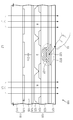
도 4은 본 발명의 일 실시예에 따른 표시장치의 단면도이다.
도 5는 도 4에 도시된 B 부분의 확대도이다.
도 6a 내지 도 6c는 본 발명의 일 실시예에 따른 외부 신호의 센싱 방법을 설명하기 위한 도면이다.
도 7은 커패시터에 충전된 전압의 변화를 도시한 파형도이다.1 is a block diagram of a display device according to an embodiment of the present invention.
2 is a circuit diagram of the plurality of sensor circuits shown in Fig.
3 is a circuit diagram of a scan driver according to an embodiment of the present invention.
4 is a cross-sectional view of a display device according to an embodiment of the present invention.
5 is an enlarged view of a portion B shown in Fig.
6A to 6C are views for explaining a method of sensing an external signal according to an embodiment of the present invention.
7 is a waveform diagram showing a change in the voltage charged in the capacitor.
이하, 첨부한 도면들을 참조하여 본 발명의 바람직한 실시예를 보다 상세하게 설명하고자 한다.Hereinafter, preferred embodiments of the present invention will be described in detail with reference to the accompanying drawings.
도 1은 본 발명의 일 실시예에 따른 표시장치의 블럭도이고, 도 2는 도 1에 도시된 다수의 센서회로의 회로도이다.FIG. 1 is a block diagram of a display device according to an embodiment of the present invention, and FIG. 2 is a circuit diagram of a plurality of sensor circuits shown in FIG.
도 1을 참조하면, 표시장치(300)는 표시패널(100), 타이밍 컨트롤러(310), 게이트 드라이버(320), 데이터 드라이버(330), 스캔 드라이버(340) 및 검출회로(350)를 포함한다.1, a
상기 타이밍 컨트롤러(310)는 상기 표시장치(300)의 외부로부터 다수의 영상신호(RGB) 및 다수의 제어신호(CS)를 수신한다. 상기 타이밍 컨트롤러(310)는 상기 데이터 드라이버(330)와의 인터페이스 사양에 맞도록 상기 영상신호들(RGB)의 데이터 포맷을 변환하고, 변환된 영상신호들(R'G'B')을 상기 데이터 드라이버(330)로 제공한다. 또한, 상기 타이밍 컨트롤러(310)는 데이터 제어신호(예를 들어, 출력개시신호(TP), 수평개시신호(STH) 등)를 상기 데이터 드라이버(330)로 제공하고, 게이트 제어신호(예를 들어, 수직개시신호(STV1), 수직클럭신호(CKV1), 및 수직클럭바신호(CKVB1))를 게이트 드라이버(320)로 제공한다.The
상기 게이트 드라이버(320)는 상기 타이밍 컨트롤러(310)로부터 제공되는 상기 게이트 제어신호(STV1, CKV1, CKVB1)에 응답해서 게이트 신호들(G1~Gn)을 순차적으로 출력한다.The
상기 데이터 드라이버(330)는 상기 타이밍 컨트롤러(310)로부터 제공되는 상기 데이터 제어신호(TP, STH, POL)에 응답해서 상기 영상신호들(R'G'B')을 데이터 전압들(D1~Dm)로 변환하여 출력한다. 상기 출력된 데이터 전압들(D1~Dm)은 상기 표시패널(100)로 인가된다.The
상기 표시패널(100)에는 다수의 화소(PX) 및 다수의 센서회로들(SN)이 구비된다. 즉, 상기 다수의 화소(PX)와 상기 다수의 센서회로들(SN)은 상기 표시패널(100)에 내장된다. 상기 표시패널(100)은 하부기판, 상기 하부기판과 마주하는 상부기판 및 상기 하부기판과 상기 상부기판 사이에 개재된 액정층으로 이루어질 수 있다. 본 발명의 일 예로, 상기 다수의 센서회로들(SN)은 상기 상부기판에 구비될 수 있다.The
상기 화소들(PX) 각각은 서로 동일한 구조를 가지므로, 여기서는 하나의 화소에 대한 구성을 일 예로써 설명하기로 한다. Since each of the pixels PX has the same structure, the configuration for one pixel will be described as an example.
상기 하부기판에는 다수의 게이트 라인들(GL), 상기 다수의 게이트 라인들 (GL)과 교차하는 다수의 데이터 라인들(DL) 및 상기 다수의 화소들(PX)이 구비된다. 도면에 도시하지는 않았지만, 각 화소(PX)는 박막 트랜지스터, 액정 커패시터 및 스토리지 커패시터를 포함할 수 있다. 상기 박막 트랜지스터의 게이트 전극은 상기 다수의 게이트 라인들(GL) 중 대응하는 게이트 라인에 연결되고, 소오스 전극은 상기 다수의 데이터 라인들(DL) 중 대응하는 데이터 라인에 연결되며, 드레인 전극은 상기 액정 커패시터 및 스토리지 커패시터에 연결될 수 있다.The lower substrate includes a plurality of gate lines GL, a plurality of data lines DL intersecting the plurality of gate lines GL, and the plurality of pixels PX. Although not shown in the figure, each pixel PX may include a thin film transistor, a liquid crystal capacitor, and a storage capacitor. A gate electrode of the thin film transistor is connected to a corresponding gate line among the plurality of gate lines GL and a source electrode is connected to a corresponding one of the plurality of data lines DL, Liquid crystal capacitors and storage capacitors.
상기 다수의 게이트 라인들(GL)은 상기 게이트 드라이버(320)에 연결되며, 상기 다수의 데이터 라인들(DL)은 상기 데이터 드라이버(330)에 연결된다. 상기 다수의 게이트 라인들(GL)은 상기 게이트 드라이버(320)로부터 제공되는 게이트 신호들(G1~Gn)을 수신하고, 상기 다수의 데이터 라인들(DL)은 상기 데이터 드라이버(330)로부터 제공되는 데이터 전압들(D1~Dm)을 수신한다.The plurality of gate lines GL are connected to the
따라서, 상기 각 화소(PX)의 박막 트랜지스터는 대응하는 게이트 라인으로 공급되는 게이트 신호에 응답하여 턴-온되고, 대응하는 데이터 라인으로 공급된 데이터 전압은 턴-온된 박막 트랜지스터를 통해 상기 액정 커패시터의 제1 전극(이하, 화소전극)에 인가된다. 한편, 상기 액정 커패시터의 제2 전극(이하, 공통전극)에는 공통전압(Vcom)이 인가된다. 상기 공통전극은 상기 상부 기판에 구비되며, 직류 전압 형태의 상기 공통전압(Vcom)이 상기 공통전극에 인가된다. 따라서, 상기 액정 커패시터에는 상기 공통전압(Vcom)과 상기 데이터 전압의 전위차에 해당하는 전압이 충전된다. 각 화소(PX)는 상기 액정 커패시터에 충전된 전압의 크기에 따라 광 투과율을 제어하여 영상을 표시할 수 있다.Accordingly, the thin film transistor of each pixel PX is turned on in response to the gate signal supplied to the corresponding gate line, and the data voltage supplied to the corresponding data line is turned on through the thin film transistor of the liquid crystal capacitor Is applied to the first electrode (hereinafter, pixel electrode). On the other hand, a common voltage Vcom is applied to the second electrode (hereinafter referred to as a common electrode) of the liquid crystal capacitor. The common electrode is provided on the upper substrate, and the common voltage Vcom in the form of a DC voltage is applied to the common electrode. Therefore, the liquid crystal capacitor is charged with the voltage corresponding to the potential difference between the common voltage Vcom and the data voltage. Each pixel PX can display an image by controlling the light transmittance according to the magnitude of the voltage charged in the liquid crystal capacitor.
한편, 상기 상부기판에는 다수의 스캔 라인들(SL), 상기 다수의 스캔 라인들(SL)과 교차하는 다수의 리드아웃 라인들(RL) 및 상기 다수의 센서회로들(SN)이 구비된다.The upper substrate includes a plurality of scan lines SL, a plurality of lead-out lines RL crossing the plurality of scan lines SL, and a plurality of the sensor circuits SN.
한편, 상기 센서회로들(SN) 각각은 서로 동일한 구조를 가지므로, 여기서는 도 2를 참조하여 하나의 센서회로(SN)에 대한 구성을 일 예로써 설명하기로 한다. 단, 도 2에서는 설명의 편의를 위하여 상기 다수의 스캔 라인(SL) 중 제1 및 제2 스캔 라인(SL1, SL2)을 도시하였고, 상기 다수의 리드아웃 라인(RL) 중 제1 및 제2 리드아웃 라인(RL1, RL2)을 도시하였다.Since each of the sensor circuits SN has the same structure, the configuration of one sensor circuit SN will be described as an example with reference to FIG. 2, the first and second scan lines SL1 and SL2 among the plurality of scan lines SL are illustrated for convenience of description, and the first and second scan lines SL1 and SL2 among the plurality of scan lines SL, The lead-out lines RL1 and RL2 are shown.
도 2를 참조하면, 각 센서회로(SN)는 제1 및 제2 스캔 라인(SL1, SL2) 및 제1 및 제2 리드아웃 라인(RL1, RL2)에 의해 구획된 영역에 구비될 수 있다. Referring to FIG. 2, each sensor circuit SN may be provided in an area partitioned by the first and second scan lines SL1 and SL2 and the first and second lead-out lines RL1 and RL2.
상기 각 센서회로는 제1 및 제2 센서(ST1, ST2), 스위칭 소자(SW) 및 커패시터(Cs)를 포함한다. 일 예로, 상기 제1 및 상기 제2 센서(ST1, ST2) 및 스위칭 소자(SW)는 각각 트랜지스터로 이루어지고, 상기 트랜지스터는 실리콘 게르마늄으로 이루어진 반도체층을 포함할 수 있다.Each sensor circuit includes first and second sensors ST1 and ST2, a switching element SW and a capacitor Cs. For example, the first and second sensors ST1 and ST2 and the switching element SW may each comprise a transistor, and the transistor may include a semiconductor layer made of silicon germanium.
상기 스위칭 소자의 게이트 전극은 상기 제1 스캔 라인(SL1)에 연결되고, 드레인 전극은 상기 제1 리드아웃 라인(RL1)에 연결되며, 소스 전극은 제3 바이어스 전압(VB3)을 공급하는 전압 라인에 연결된다. The gate electrode of the switching element is connected to the first scan line SL1, the drain electrode is connected to the first lead-out line RL1, and the source electrode of the switching element is connected to the voltage line VB3 for supplying the third bias voltage VB3. Lt; / RTI >
상기 제1 및 제2 센서(ST1, ST2)는 서로 다른 외부 신호를 각각 센싱하고, 상기 외부 신호들에 따라 가변되는 전류 신호를 각각 출력한다. The first and second sensors ST1 and ST2 respectively sense different external signals and output a variable current signal according to the external signals.
상기 제1 센서(ST1)는 가시광선 파장대를 갖는 제1 광을 센싱한다. 상기 제1 센서(ST1)의 게이트 전극은 제1 바이어스 전압(VB1)을 공급하는 전압 라인에 연결되고, 소스 전극은 제2 바이어스 전압(VB2)을 공급하는 전압 라인에 연결되고, 상기 드레인 전극은 출력 단자에 연결된다. 상기 제1 바이어스 전압(VB1)은 음의 값을 가질 수 있다. The first sensor ST1 senses a first light having a visible light wavelength band. A gate electrode of the first sensor ST1 is connected to a voltage line for supplying a first bias voltage VB1 and a source electrode is connected to a voltage line for supplying a second bias voltage VB2, Output terminal. The first bias voltage VB1 may have a negative value.
한편, 상기 제2 센서(ST2)는 적외선 파장대를 갖는 제2 광을 센싱한다. 상기 제2 센서(ST2)의 상기 제1 센서(ST1)와 마찬가지로 게이트 전극은 제1 바이어스 전압(VB1)을 공급하는 전압 라인에 연결되고, 소스 전극은 제2 바이어스 전압(VB2)을 공급하는 전압 라인에 연결되고, 상기 드레인 전극은 출력 단자에 연결된다. 상기 제1 센서(ST1) 및 상기 제2 센서(ST2)는 동일한 출력 단자에 공통으로 연결될 수 있다. 상기 제2 센서(ST2)는 가시광선 파장대를 갖는 제1 광을 차단하고, 적외선 파장대를 갖는 제2 광을 투과시키는 적외선 필터를 포함할 수 있다. Meanwhile, the second sensor ST2 senses a second light having an infrared wavelength band. Like the first sensor ST1 of the second sensor ST2, the gate electrode is connected to the voltage line for supplying the first bias voltage VB1, and the source electrode is connected to the voltage for supplying the second bias voltage VB2 Line, and the drain electrode is connected to an output terminal. The first sensor ST1 and the second sensor ST2 may be commonly connected to the same output terminal. The second sensor ST2 may include an infrared ray filter for blocking first light having a visible light wavelength band and transmitting second light having an infrared wavelength band.
상기 커패시터(Cs)는 상기 대응하는 스캔 라인(SL1)과 상기 제1 및 상기 제2 센서(ST1, ST2) 사이에 구비된다. 구체적으로 상기 커패시터(Cs)는 상기 스위칭 소자(SW)의 게이트 전극과 전기적으로 연결된 제1 전극 및 상기 제1 및 상기 제2 센서(ST1, ST2)의 출력 단자와 전기적으로 연결된 제2 전극을 포함한다. The capacitor Cs is provided between the corresponding scan line SL1 and the first and second sensors ST1 and ST2. More specifically, the capacitor Cs includes a first electrode electrically connected to the gate electrode of the switching device SW and a second electrode electrically connected to the output terminals of the first and second sensors ST1 and ST2 do.
상기 제1 전극은 상기 스위칭 소자(SW)의 게이트 전극과 동일한 스캔 라인(SL2)에 연결된다. 또한, 도 2에 도시된 바처럼, 상기 커패시터(Cs)의 제1 전극은 상기 스위칭 소자(SW)의 게이트 전극과 일체로 형성될 수 있다. The first electrode is connected to the same scan line SL2 as the gate electrode of the switching element SW. Also, as shown in FIG. 2, the first electrode of the capacitor Cs may be formed integrally with the gate electrode of the switching device SW.
상기 커패시터(Cs)는 상기 제1 스캔 라인(SL1)으로부터 스캔 신호를 수신하여 제1 전압을 충전하고, 상기 스캔 신호의 공급이 끝난 뒤 상기 제1 스캔 라인(SL1)이 플로팅된 이후에 상기 전류 신호에 의해 제1 전압보다 큰 제2 전압을 충전한다. The capacitor Cs receives the scan signal from the first scan line SL1 and charges the first voltage. After the first scan line SL1 is floated after the supply of the scan signal, And charges the second voltage higher than the first voltage by the signal.
이 때, 상기 제1 스캔 라인(SL1)을 통해 상기 스위칭 소자(SW)의 문턱 전압의 크기보다 낮은 크기의 스캔 신호가 인가되므로, 상기 제1 전압은 상기 스위칭 소자(SW)의 문턱 전압보다 낮고, 상기 제2 전압은 상기 스위칭 소자(SW)의 문턱 전압보다 높다. 따라서, 상기 스위칭 소자(SW)는 상기 커패시터(Cs)에 충전된 상기 제2 전압에 응답하여 턴-온되고, 상기 센싱 신호를 상기 대응하는 리드아웃 라인(RL1)으로 출력한다. At this time, since a scan signal having a magnitude lower than the threshold voltage of the switching element SW is applied through the first scan line SL1, the first voltage is lower than the threshold voltage of the switching element SW , And the second voltage is higher than the threshold voltage of the switching element SW. Accordingly, the switching element SW is turned on in response to the second voltage charged in the capacitor Cs, and outputs the sensing signal to the corresponding lead-out line RL1.
상기 다수의 스캔 라인들(SL)은 상기 스캔 드라이버(340)에 연결되어 다수의 스캔 신호들을 각각 수신한다. 상기 스캔 드라이버(340)는 상기 타이밍 컨트롤러(310)로부터 스캔 제어신호(예를 들어, 개시신호(STV2), 제1 및 제2 클럭신호(CKV2, CKVB2))를 수신하여 상기 스캔 신호들을 출력한다. 상기 스캔 제어신호(STV2, CK2, CKB2)는 게이트 제어신호(STV1, CKV1, CKVB1)에 동기하는 신호일 수 있다. 상기 스캔 드라이버(340)의 구성 및 동작에 대해서는 도 3을 참조하여 자세하게 설명한다.The plurality of scan lines SL are connected to the
도 2에 도시된 센서회로들(SN)은 서로 다른 외부 신호를 수신하는 다수의 센서들이 하나의 스위칭 소자에 공통으로 연결되어, 스위칭 소자 및 배선의 수를 줄일 수 있고, 회로를 단순하게 구현할 수 있다. 따라서, 동일한 면적 내에 삽입되는 센서의 수를 증가시킬 수 있으므로 터치 회로의 해상도(resolution)가 높아져 터치 위치를 보다 정확하게 센싱할 수 있다.In the sensor circuits SN shown in FIG. 2, a plurality of sensors receiving different external signals are commonly connected to one switching element, so that the number of switching elements and wiring can be reduced, and a circuit can be simply implemented have. Accordingly, since the number of sensors inserted in the same area can be increased, the resolution of the touch circuit is increased, and the touch position can be more accurately sensed.
도 3은 본 발명의 일 실시예에 따른 스캔 드라이버의 구성을 개념적으로 도시한 회로도이다. 도 3을 참조하면, 상기 스캔 드라이버(340)는 쉬프트 레지스터(341), 반전회로(342) 및 스위칭 회로(343)를 포함한다.3 is a circuit diagram conceptually illustrating a configuration of a scan driver according to an embodiment of the present invention. Referring to FIG. 3, the
상기 쉬프트 레지스터(341)는 서로 종속적으로 연결된 다수의 스테이지(SRC1~SRCn+1)로 이루어진다. 각 스테이지는 제1 입력단자(IN1), 제1 및 제2 클럭단자(CK1, CK2), 제2 입력단자(IN2), 전압입력단자(Vin), 리셋단자(RE) 및 출력단자(OUT)를 포함한다.The
상기 다수의 스테이지(SRC1 ~ SRCn+1)의 제1 입력단자(IN1)는 이전단 스테이지의 출력단자(OUT)에 전기적으로 연결되어 이전단 베이스 신호(BS1~BSn)를 입력받는다. 단, 상기 다수의 스테이지(SRC1 ~ SRCn+1) 중 첫번째 스테이지(SRC1)의 제1 입력단자(IN1)에는 상기 스캔 드라이버(340)의 구동을 개시하는 개시신호(STV)가 제공된다. 상기 다수의 스테이지(SRC1 ~ SRCn+1)의 제2 입력단자(IN2)는 다음단 스테이지의 출력단자(OUT)에 전기적으로 연결되어 다음단 베이스 신호(BS2~BSn+1)를 입력받는다. 단, 상기 다수의 스테이지(SRC1 ~ SRCn+1) 중 마지막 스테이지(SRCn+1)의 제2 입력단자(IN2)에는 상기 개시신호(STV2)가 제공된다.The first input terminal IN1 of the plurality of stages SRC1 to SRCn + 1 is electrically connected to the output terminal OUT of the previous single stage to receive the previous stage base signals BS1 to BSn. A start signal STV for starting the driving of the
상기 다수의 스테이지(SRC1 ~ SRCn+1) 중 홀수번째 스테이지(SRC1, SRC3,...SRCn+1)의 제1 클럭단자(CK1)에는 제1 클럭(CKV2)이 제공되고, 제2 클럭단자(CK2)에는 상기 제1 클럭(CKV2)과 반전된 위상을 갖는 제2 클럭(CKVB2)이 제공된다. 상기 다수의 스테이지(SRC1 ~ SRCn+1) 중 짝수번째 스테이지(SRC2,...SRCn)의 제1 클럭단자(CK1)에는 상기 제2 클럭(CKVB2)이 제공되고, 제2 클럭단자(CK2)에는 상기 제1 클럭(CKV2)이 제공된다.The first clock CKV2 is provided to the first clock terminal CK1 of the odd-numbered stages SRC1, SRC3, ...
상기 다수의 스테이지(SRC1 ~ SRCn+1)의 전압입력단자(Vin)에는 접지전압 또는 게이트 오프전압(VSS)이 제공된다. 또한, 상기 마지막 스테이지(SRCn+1)의 출력단자(OUT)는 다수의 스테이지(SRC1 ~ SRCn+1)의 리셋단자(RE)에 전기적으로 연결된다.The voltage input terminal Vin of the stages SRC1 to SRCn + 1 is provided with a ground voltage or a gate off voltage VSS. The output terminal OUT of the last stage SRCn + 1 is electrically connected to the reset terminal RE of the plurality of stages SRC1 to
상기 다수의 스테이지(SRC1 ~ SRCn)의 출력단자(OUT)들은 상기 다수의 반전 회로(342) 각각에 일대일 대응하여 전기적으로 연결된다. 상기 반전회로(342)는 상기 쉬프트 레지스터(341)의 상기 다수의 스테이지(SRC1 ~ SRCn)의 출력단자(OUT) 각각에 연결되어, 출력된 베이스 신호들(BS1~BSn) 각각을 반전하여 각각의 스캔 신호들(SC1~SCn)을 출력한다. 이 때, 상기 스캔 신호들(SC1~SCn)에 의해 상기 스위칭 소자(SW)가 턴-온되는 것을 방지하기 위해, 상기 스캔 신호들(SC1~SCn)의 크기는 상기 스위칭 소자(SW)의 문턱 전압보다 낮은 값으로 정해진다. The output terminals OUT of the plurality of stages SRC1 to SRCn are electrically connected to each of the plurality of inverting
상기 스위칭 회로(343)는 상기 반전 회로(342)의 출력단자에 연결되고, 스위칭 신호들(SH1~SHn)에 응답하여 상기 스캔 라인들(SL1~SLn) 각각을 플로팅시킨다. 상기 스위칭 신호들(SH1~SHn)은 상기 스캔 라인들(SL1~SLn)에 순차적으로 인가되므로, 상기 스캔 라인들(SL1~SLn) 각각은 순차적으로 플로팅된다. 이때, 상기 스위칭 신호들(SH1~SHn)은 상기 베이스 신호들(BS1~BSn) 각각과 동기화되어 인가될 수 있으며, 상기 스위칭 신호들(SH1~SHn)은 상기 베이스 신호들(BS1~BSn)과 동일할 수 있다. The
다시 도 1 및 도 2를 참조하면, 상기 리드아웃 라인들(RL)은 상기 검출 회로(350)에 연결되어 대응하는 센서회로들(SN)로부터 수신한 센싱 신호를 상기 검출 회로(350)로 제공하는 역할을 수행한다. 상기 센서회로(SN)는 상기 제2 전압에 응답하여 상기 스위칭 소자(SW)가 턴-온되면, 상기 턴-온된 스위칭 소자(SW)를 통해 상기 외부 신호의 세기에 따른 센싱 신호를 상기 제1 리드아웃 라인(RL1)으로 제공한다.1 and 2, the lead-out lines RL are connected to the
상기 검출회로(350)는 상기 센싱 신호를 수신하여 상기 외부 신호들이 제공된 위치를 검출한다. 구체적으로, 상기 검출회로(350)는 상기 베이스 신호가 발생된 시점 및 상기 수신된 센싱 신호를 근거로 위치 정보(PS), 즉 상기 사용자가 손가락으로 터치한 지점의 2차원 좌표값을 생성할 수 있다. The
상기 검출회로(350)는 타이밍 컨트롤러(310)를 통해 상기 위치 정보(PS)를 처리장치(미도시)로 전송한다, 상기 처리장치는 수신한 상기 위치 정보(PS)를 근거로 사용자가 표시패널 상에서 상기 위치 정보가 가리키는 위치에 표시된 컴포넌트를 선택한 것으로 간주한다. 그리고, 상기 처리장치(미도시)는 상기 컴포넌트의 선택에 따른 명령을 처리하고, 처리 결과에 따른 새로운 영상 신호(R, G, B) 및 제어신호(CS)를 상기 타이밍 컨트롤러(310)로 전송한다. 상기 표시장치(300)는 수신한 신호(R,G,B, CS)들을 기초로 처리 결과를 표시한다.The
도 4은 본 발명의 일 실시예에 따른 표시장치의 단면도이고, 도 5는 도 4에 도시된 B 부분의 확대도이다.FIG. 4 is a cross-sectional view of a display device according to an embodiment of the present invention, and FIG. 5 is an enlarged view of a portion B shown in FIG.
도 4 및 도 5를 참조하면, 표시장치(300)는 영상을 표시하는 표시패널(100) 및 상기 표시패널(100)의 하부에 구비된 백라이트 유닛(200)을 포함한다.4 and 5, the
도 5를 참조하면, 상기 표시패널(100)은 하부기판(110), 상기 하부기판(110)과 마주하는 상부기판(120) 및 상기 하부기판(110)과 상기 상부기판(120) 사이에 개재된 액정층(130)으로 이루어진다.5, the
상기 하부기판(110)은 제1 베이스 기판(111) 및 상기 제1 베이스 기판(111) 상에 구비된 다수의 화소(PX, 도 1에 도시됨)를 포함한다. 각 화소(PX)에는 화소전극(115)이 포함될 수 있다. 그러나, 각 화소는 화소전극(115) 이외에도 상기 화소전극(115)을 구동시키기 위한 박막 트랜지스터 등을 더 포함할 수 있다.The
상기 상부기판(120)은 상기 제1 베이스 기판(111)과 마주하는 제2 베이스 기판(121) 및 상기 하부기판(110)과 마주하는 상기 제2 베이스 기판(121)의 하면 상에 구비된 다수의 센서회로들(SN, 도 1에 도시됨)을 포함한다. 상기 다수의 센서회로들(SN) 각각에 포함된 센서들(ST1, ST2, 도 1에 도시됨)은 실리콘 게르마늄(SiGe) 트랜지스터로 이루어져 상기 제2 베이스 기판(112) 상에 형성될 수 있다. 도 5에는 편의상 제2 센서(ST2)만을 도시하였다. 이때, 상기 제2 센서(ST2)는 반도체층(127) 하부에 구비되어서 상기 제2 광(L2)을 통과시키고 상기 제1 광(L1)은 차단하는 필터(122)를 더 포함할 수 있다. 상기 필터(122)는 상기 반도체층과 마찬가지로 실리콘 게르마늄(SiGe)으로 이루어질 수 있다.The
또한, 상기 상부 기판(120)은 센서회로들(SN)을 커버하는 절연막(123), 상기 절연막(123) 상에 상기 화소전극(115)과 마주하는 영역에 배치된 레드, 그린 및 블루 색화소들(R, G, B)를 더 포함한다. 상기 색화소들(R, G, B) 사이에는 블랙 매트릭스(124)가 구비되며, 상기 색화소들(R, G, B)은 유기 절연막(125)에 의해서 커버된다. 상기 상부 기판(120)은 상기 유기 절연막(125)상에 형성된 공통전극(126)을 더 포함한다.The
상기 화소전극(115), 상기 공통전극(126) 및 상기 액정층(130)에 의해서 액정 커패시터(Clc)가 형성될 수 있다.The liquid crystal capacitor Clc may be formed by the
도 5에서는 상기 색화소들(R, G, B)이 상기 상부기판(120) 측에 구비된 구조를 제시하였으나, 상기 색화소들(R,G,B)은 상기 하부기판(110) 측에 구비될 수도 있다.Although the color pixels R, G and B are provided on the
도 4를 참조하면, 상기 백라이트 유닛(200)은 상기 표시패널(100)의 하부에 배치된 회로기판(201), 상기 회로기판(201) 상에 실장되어 가시광선 파장대를 갖는 제1 광(L1)을 출사하는 다수의 제1 광원(210) 및 상기 회로기판(201) 상에 실장되어 적외선 파장대를 갖는 제2 광(L2)을 출사하는 다수의 제2 광원(220)을 포함한다. 4, the
상기 제1 및 제2 광원들(210, 220)은 상기 회로기판(201) 상에 교번적으로 배치될 수 있다. 본 발명의 일 예로, 도 4에 도시된 바와 같이 서로 인접하는 두 개의 제1 광원(210) 사이에 하나의 제2 광원(220)이 배치될 수 있다. 또한, 상기 제1 및 제2 광원들(210, 220) 각각은 발광 다이오드로 이루어질 수 있다.The first and second
도 5을 참조하면, 상기 제1 광원들(210)로부터 출사된 상기 제1 광(L1)은 상기 표시패널(100)로 입사되고, 입사된 상기 제1 광(L1)은 상기 액정층(130)을 통과한다. 상기 액정층(130)의 광 투과율은 상기 화소전극(115)과 상기 공통전극(124) 사이에 형성된 전계에 의해서 컨트롤된다. 즉, 상기 표시패널(100)은 상기 액정층(130)에 의해서 상기 제1 광(L1)의 투과율을 컨트롤함으로써 원하는 계조의 영상을 표시할 수 있다. 5, the first light L1 emitted from the
한편, 상기 제2 광원들(220)로부터 출사된 상기 제2 광(L2)은 상기 표시패널(100)로 입사된 후 상기 표시패널(100)을 통과한다. 상기 표시패널(100)을 통과한 상기 제2 광(L2)은 사용자의 눈에는 인식되지 않으므로, 상기 사용자가 상기 표시패널(100)에 표시된 영상을 인식하는 데에는 영향을 미치지 않는다.Meanwhile, the second light L2 emitted from the second
상기 제2 광원들(220)로부터 출사된 상기 제2 광(L2)은 상기 표시패널(100) 내에 구비된 다수의 층(예컨데, 화소전극(115), 액정층(130) 및 색화소(R,G,B) 등에 의해서 일부 반사되고, 일부만이 상기 표시패널(100)을 통과할 수 있다. The second light L2 emitted from the second
상기 표시패널(100)을 통과한 상기 제1 광(L1) 및 상기 제2 광(L2)은 외부로 방사되지만, 상기 표시패널(100) 상에 물체(예를 들어, 손가락)(10)가 존재하면, 상기 손가락(10)에 의해서 반사될 수 있다. 상기 표시패널(100) 상의 물체에 의해 반사된 상기 제1 광(L1)은 상기 제1 센서(미도시)에 의해 센싱될 수 있고, 반사된 상기 제2 광(L2)은 상기 제2 센서(ST2)에 의해 센싱될 수 있다. 그러나, 제1 광(L1)은 블랙 계조를 나타내는 영역에서는 상기 액정층(130)에 의해 차단되므로, 이 경우에는 제2 광(L2)에 의한 센싱만이 가능하다. 다시 말해, 본 발명에서는 센싱의 정확도를 높이기 위해, 복수의 광원 및 서로 다른 파장대의 광을 센싱하는 센서들을 사용한다.The first light L1 and the second light L2 having passed through the
본 발명의 일 예로, 도 5에서는 사용자가 상기 손가락(10)을 이용하여 상기 표시패널(100)의 특정 지점을 터치한 경우를 도시하였고, 특히 상기 손가락(10)에 의해서 상기 제2 광(L2)이 반사된 것을 예로 들었다.5 shows a case where a user touches a specific point of the
상기 손가락(10)에 의해서 반사된 상기 제2 광(L2)은 표시패널(100) 내에 구비된 상기 제2 센서(ST2)를 통해 센싱될 수 있다. 상기 반사된 상기 제2 광(L2)은 상기 필터(122)를 통과하여 상기 제2 센서(ST2)의 반도체층(127)으로 입사되고, 상기 반사된 상기 제2 광(L2)의 광량에 따라 상기 제2 센서(ST2)로부터 출력되는 포토 전류가 변화된다. The second light L2 reflected by the
도 5에서는, 상기 제2 센서(ST2)가 상기 상부 기판(120)에 구비된 구조를 제시하였으나, 상기 센서들은 상기 하부 기판상에 구비될 수도 있다.In FIG. 5, the second sensor ST2 is provided on the
그러나, 상기 센서들이 상기 상부기판(120)에 구비되면, 상기 하부기판(110)에 구비된 경우에 비하여 상기 물체와의 거리가 상대적으로 가까워진다. 따라서, 상기 센서(ST1, ST2)의 감도를 향상시킬 수 있고, 상기 터치된 지점을 정확하게 파악하는데 유리할 수 있다. 또한, 상기 상부기판(120)에 구비된 상기 센서(ST1)가 블랙 매트릭스(123)가 형성된 영역 내에 위치하는 경우, 상기 표시패널(100)의 개구율이 향상될 수 있다.However, when the sensors are provided on the
이하, 상기 센서회로의 외부 신호의 센싱 방법에 대해 구체적으로 설명하도록 한다. 상기 센서회로들(SN) 각각은 서로 동일한 구조를 가지므로, 여기서는 도 6A 내지 6C를 참조하여 하나의 센서회로(SN)의 동작을 일 예로써 설명하기로 한다. 단, 6A 내지 6C에서는 설명의 편의를 위하여 상기 센서회로(SN)에 대응하는 제1 스캔 라인(SL1) 및 제1 리드아웃 라인(RL1) 만을 도시하였다.Hereinafter, a method of sensing an external signal of the sensor circuit will be described in detail. Since each of the sensor circuits SN has the same structure, the operation of one sensor circuit SN will be described by way of example with reference to FIGS. 6A to 6C. 6A to 6C, only the first scan line SL1 and the first lead-out line RL1 corresponding to the sensor circuit SN are illustrated for convenience of explanation.
도 6A 내지 도 6C는 본 발명의 일 실시예에 따른 외부 신호의 센싱 방법을 설명하기 위한 도면이고, 도 7은 도 6A 내지 도 6C의 커패시터에 충전된 전압의 변화를 도시한 파형도이다. 도 6C는 다시 스캔 신호가 인가되었을 때의 센서회로의 동작을 도시한 도면이다.6A to 6C are diagrams for explaining a method of sensing an external signal according to an embodiment of the present invention, and FIG. 7 is a waveform diagram showing a change in voltage charged in the capacitors of FIGS. 6A to 6C. 6C is a diagram showing the operation of the sensor circuit when the scan signal is applied again.
도 6A는 스캔 신호가 인가되었을 때의 센서회로의 동작을 도시한 도면으로 도 7에서 0과 t1까지의 구간에 대응한다.FIG. 6A is a diagram showing the operation of the sensor circuit when a scan signal is applied, and corresponds to a period from 0 to t1 in FIG.
도 6A 및 도 7을 참조하면, 상기 커패시터(Cs)는 상기 제1 스캔 라인(SL1)으로부터 인가된 스캔 신호(SC)를 수신하여 커패시터(Cs) 양단에 제1 전압(V1)을 충전한다. 전술한 바와 같이, 상기 제1 스캔 라인(SL1)으로부터 스위칭 소자(SW)의 문턱 전압보다 낮은 스캔 신호가 인가되므로, 상기 제1 전압(V1)은 상기 스위칭 소자(SW)의 문턱 전압(Vt)보다 낮고, 스위칭 소자(SW)는 턴-오프된 상태를 유지한다.6A and 7, the capacitor Cs receives the scan signal SC applied from the first scan line SL1 and charges the first voltage V1 across the capacitor Cs. The first voltage V1 is lower than the threshold voltage Vt of the switching device SW because a scan signal lower than the threshold voltage of the switching device SW is applied from the first scan line SL1, And the switching element SW maintains the turned-off state.
도 6B는 대응하는 스캔 라인이 플로팅 된 후에 외부 신호가 센싱되었을 때의 센서회로의 동작을 도시한 도면으로, 도 7에서 t1과 t2 사이의 구간에 대응한다.FIG. 6B is a diagram showing the operation of the sensor circuit when an external signal is sensed after the corresponding scan line is floated, and corresponds to a section between t1 and t2 in FIG.
도 6B 및 도 7을 참조하면, 스캔 신호(SC)의 공급이 중지되어 스캔 라인(SL2)이 플로팅되면, 상기 커패시터(Cs)는 충전된 상기 제1 전압(V1)을 유지한다. 이때, 표시패널상의 물체에 의해 상기 제1 센서(ST1)로 반사된 상기 제1 광(L1)이 입사되는 경우, 상기 제1 센서(ST1)는 입사된 광량에 따라 전류 신호를 출력한다. 마찬가지로, 상기 제2 센서(ST2)로 반사된 상기 제2 광(L2)이 입사되는 경우, 상기 제2 센서(ST2)는 입사된 광량에 따라 전류 신호를 출력한다. 만약 반사된 상기 제1 광(L1)이 상기 제1 센서(ST1)로 입사되고, 반사된 상기 제2 광(L2)이 상기 제2 센서(ST2)로 입사되는 경우, 상기 제1 및 상기 제2 센서(ST1, ST2) 각각은 각각의 센서로 입사된 광량에 따라 전류 신호(p-current)를 출력한다.Referring to FIGS. 6B and 7, when the supply of the scan signal SC is stopped and the scan line SL2 is floated, the capacitor Cs holds the charged first voltage V1. At this time, when the first light (L1) reflected by the object on the display panel is incident on the first sensor (ST1), the first sensor (ST1) outputs a current signal according to the amount of incident light. Similarly, when the second light L2 reflected by the second sensor ST2 is incident, the second sensor ST2 outputs a current signal according to the amount of incident light. If the reflected first light L1 is incident on the first sensor ST1 and the reflected second light L2 is incident on the second sensor ST2, Each of the two sensors ST1 and ST2 outputs a current signal p-current according to the amount of light incident on each sensor.
상기 전류 신호(p-current)에 의해 상기 커패시터(Cs)의 전압은 상승한다. 따라서, 상기 커패시터(Cs)에는 제1 전압(V1)보다 큰 제2 전압(V2)이 충전될 수 있다. The voltage of the capacitor Cs rises due to the current signal p-current. Therefore, the capacitor Cs may be charged with the second voltage V2, which is larger than the first voltage V1.
전술한 바와 같이, 상기 제2 전압(V2)은 상기 스위칭 소자(SW)의 문턱 전압(Vt)보다 높은 값을 갖고, 상기 커패시터(Cs)의 제1 전극은 상기 스위칭 소자(SW)에 전기적으로 연결된다. 따라서, 상기 스위칭 소자(SW)는 상기 제2 전압(V2)에 의해 턴-온이 되고, 제1 리드아웃 라인(RL1)으로 센싱 신호를 출력한다. 스위칭 소자(SW)의 소스 전극에는 직류 전압이 인가되어 있으나, 트랜지스터의 특성상 선형 영역(linear region)에서 상기 센싱 신호의 크기는 문턱 전압에 비례하여 출력된다. As described above, the second voltage V2 has a value higher than the threshold voltage Vt of the switching element SW, and the first electrode of the capacitor Cs is electrically connected to the switching element SW . Therefore, the switching element SW is turned on by the second voltage V2, and outputs the sensing signal to the first lead-out line RL1. The DC voltage is applied to the source electrode of the switching element SW, but the magnitude of the sensing signal in a linear region is proportional to the threshold voltage.
출력된 상기 센싱 신호는 상술한 바와 같이 도 1의 검출회로(350)로 인가되고, 검출회로(350)는 상기 센싱 신호를 수신하여 상기 외부 신호들이 제공된 위치를 검출한다. 또한, 상기 검출회로(350)는 타이밍 컨트롤러(310)를 통해 상기 위치 정보(PS)를 처리장치로 전송한다. 상기 타이밍 컨트롤러(310)는 상기 위치 정보에 해당하는 위치를 선택함으로써 발생된 이벤트의 처리 결과에 따른 새로운 영상 신호(R, G, B) 및 제어신호(CS)수신하고, 이를 토대로 상기 표시패널(100)은 처리 결과를 표시한다.The sensing signal is applied to the
도 6C는 스캔라인이 플로팅 된 이후 스캔 라인에 다시 스캔 신호가 인가되었을 때의 센서회로의 동작을 도시한 도면이다.6C is a view showing the operation of the sensor circuit when a scan signal is applied to the scan line after the scan line is floated.
도 6C 및 도 7을 참조하면, 상기 커패시터(Cs)는 도 6A와 마찬가지로 상기 스캔 라인(SL2)으로부터 인가된 스캔 신호(SC)를 수신하여 커패시터(Cs) 양단에 상기 제1 전압(V1)을 충전한다. 다시 말해서, 상기 커패시터(Cs)에 충전된 전압은 상기 제2 전압(V2)에서 상기 제1 전압(V1)으로 낮아지게 된다. 따라서, 상기 스위칭 소자(SW)는 턴-오프된다. 6C and FIG. 7, the capacitor Cs receives the scan signal SC applied from the scan line SL2 and applies the first voltage V1 to both ends of the capacitor Cs Charge. In other words, the voltage charged in the capacitor Cs is lowered from the second voltage V2 to the first voltage V1. Therefore, the switching element SW is turned off.
상술한 바에 따르면, 입사된 광에 의해 스위칭 소자가 턴-온되고, 트랜지스터의 액티브 영역에서 상기 스위칭 소자가 동작한다. 따라서, 상기 스위칭 소자로부터 출력되는 센싱 신호의 크기가 기존의 방식에 비해 크고 센싱 신호의 출력범위도 넓으므로, 센싱 감도가 향상된다. According to the above description, the switching element is turned on by the incident light, and the switching element operates in the active region of the transistor. Therefore, the sensing signal output from the switching element is larger than that of the conventional method, and the output range of the sensing signal is also wider, so that the sensing sensitivity is improved.
이상 실시예를 참조하여 설명하였지만, 해당 기술 분야의 숙련된 당업자는 하기의 특허 청구의 범위에 기재된 본 발명의 사상 및 영역으로부터 벗어나지 않는 범위 내에서 본 발명을 다양하게 수정 및 변경시킬 수 있음을 이해할 수 있을 것이다.It will be understood by those skilled in the art that various changes in form and details may be made therein without departing from the spirit and scope of the invention as defined in the appended claims. It will be possible.
100: 표시패널 200: 백라이트 300: 표시장치
310: 타이밍 컨트롤러 320: 게이트 드라이버
330: 데이터 드라이버 340: 스캔 드라이버 350: 검출회로
SN: 센서회로 SW: 스위칭 소자 ST1, ST2: 센서
Cs: 커패시터 SL: 스캔라인 RL: 리드아웃 라인100: display panel 200: backlight 300: display device
310: timing controller 320: gate driver
330: Data driver 340: Scan driver 350: Detection circuit
SN: sensor circuit SW: switching element ST1, ST2: sensor
Cs: capacitor SL: scan line RL: lead out line
Claims (17)
각각 적어도 2개 이상의 서로 다른 외부 신호들을 센싱하여 센싱 신호를 출력하는 다수의 센서회로; 및
상기 센싱 신호를 수신하여 상기 외부 신호들이 제공된 위치를 검출하는 검출회로를 구비하고,
각 센서회로는,
각각 서로 다른 외부 신호들을 센싱하고, 센싱된 외부 신호들에 따라 가변되는 전류신호를 출력하는 출력 단자를 공유하는 다수의 센서;
스캔 신호를 수신하는 스캔 라인;
상기 스캔 라인과 상기 출력단자 사이에 구비되고, 상기 스캔 신호를 수신하여 제1 전압을 충전하고, 상기 스캔 라인이 플로팅된 이후에 상기 전류 신호에 의해 상기 제1 전압보다 큰 제2 전압을 충전하는 커패시터;
상기 제2 전압에 응답하여 상기 센싱 신호를 출력하는 스위칭 소자; 및
상기 스위칭 소자로부터 출력된 상기 센싱 신호를 상기 검출 회로에 공급하는 리드아웃 라인을 포함하는 것을 특징으로 하는 표시장치.A display panel including a plurality of pixels for displaying an image;
A plurality of sensor circuits each sensing at least two or more different external signals to output a sensing signal; And
And a detection circuit for receiving the sensing signal and detecting a position where the external signals are provided,
Each sensor circuit includes:
A plurality of sensors that each sense different external signals and share an output terminal that outputs a varying current signal according to sensed external signals;
A scan line for receiving a scan signal;
A scan line driving circuit which is provided between the scan line and the output terminal and receives the scan signal to charge the first voltage and charges the second voltage larger than the first voltage by the current signal after the scan line is floated Capacitor;
A switching element for outputting the sensing signal in response to the second voltage; And
And a lead-out line for supplying the sensing signal output from the switching element to the detection circuit.
상기 제2 전압은 상기 스위칭 소자의 문턱 전압보다 높은 것을 특징으로 하는 표시 장치.The method of claim 1, wherein the first voltage is lower than a threshold voltage of the switching element,
Wherein the second voltage is higher than a threshold voltage of the switching element.
상기 스캔 라인에 연결되어 상기 스캔 신호를 공급하는 스캔 드라이버를 더 포함하는 것을 특징으로 하는 표시장치.The method according to claim 1,
And a scan driver coupled to the scan line to supply the scan signal.
베이스 신호를 출력하는 쉬프트 레지스터;
상기 쉬프트 레지스터로부터 수신된 베이스 신호를 반전하여 상기 스캔 신호를 출력하는 반전 회로; 및
상기 반전회로의 출력단에 연결되고 스위칭 신호에 응답하여 소정 구간 동안 상기 스캔 라인을 플로팅시키는 스위칭 회로를 포함하는 것을 특징으로 하는 표시장치.4. The method of claim 3, wherein the scan driver
A shift register for outputting a base signal;
An inversion circuit for inverting the base signal received from the shift register and outputting the scan signal; And
And a switching circuit connected to an output terminal of the inversion circuit and floating the scan line for a predetermined period in response to a switching signal.
가시광선 파장대를 갖는 제1 광을 센싱하는 제1 센서; 및
적외선 파장대를 갖는 제2 광을 센싱하는 제2 센서를 포함하는 것을 특징으로 하는 표시 장치.The apparatus of claim 1, wherein each of the plurality of sensors comprises:
A first sensor for sensing a first light having a visible light wavelength band; And
And a second sensor for sensing a second light having an infrared wavelength band.
제1 바이어스 전압을 공급하는 전압 라인에 연결된 게이트 전극, 제2 바이어스 전압을 공급하는 전압 라인에 연결된 소스 전극 및 상기 출력 단자에 연결된 드레인 전극을 포함하는 것을 특징으로 하는 표시 장치. 6. The apparatus of claim 5, wherein each of the first sensor and the second sensor comprises:
A gate electrode connected to a voltage line for supplying a first bias voltage, a source electrode connected to a voltage line for supplying a second bias voltage, and a drain electrode connected to the output terminal.
상기 스캔 라인에 연결된 게이트 전극, 상기 리드아웃 라인에 연결된 드레인 전극 및 제3 바이어스 전압을 공급하는 전압 라인에 연결된 소스 전극을 포함하는 것을 특징으로 하는 표시 장치.8. The switching device according to claim 7,
A gate electrode connected to the scan line, a drain electrode connected to the lead-out line, and a source electrode connected to a voltage line for supplying a third bias voltage.
상기 스위칭 소자의 게이트 전극과 전기적으로 연결된 제1 전극 및 상기 제1 및 상기 제2 센서의 출력 단자에 전기적으로 연결된 제2 전극에 의해 정의되는 것을 특징으로 하는 표시장치9. The apparatus of claim 8,
A first electrode electrically connected to the gate electrode of the switching element and a second electrode electrically connected to the output terminals of the first and second sensors.
상기 센서회로는 상기 상부 기판 상에 구비되는 것을 특징으로 하는 표시장치.14. The display device according to claim 13, wherein the display panel includes an upper substrate and a lower substrate,
And the sensor circuit is provided on the upper substrate.
스캔 신호를 인가하여 커패시터에 제1 전압을 충전하는 단계;
상기 스캔 신호의 공급이 끝난 뒤 상기 제1 및 상기 제2 센서 중 적어도 하나로부터 센싱된 외부 신호에 대응하는 전류 신호에 의해 상기 커패시터에 상기 제1 전압보다 큰 제2 전압을 충전하는 단계;
상기 제2 전압에 응답하여 스위칭 소자가 센싱 신호를 출력하는 단계;
상기 센싱 신호를 근거로 상기 외부 신호가 제공된 위치를 나타내는 위치 정보를 산출 및 출력하는 단계; 및
표시패널에 상기 위치 정보를 기초로 발생한 이벤트의 처리결과를 표시하는 단계를 포함하는 표시장치의 구동 방법. A method of driving a display device including first and second sensors for sensing different external signals,
Applying a scan signal to charge a first voltage to a capacitor;
Charging the capacitor with a second voltage greater than the first voltage by a current signal corresponding to an external signal sensed from at least one of the first and second sensors after the supply of the scan signal is completed;
The switching element outputting a sensing signal in response to the second voltage;
Calculating and outputting position information indicating a position where the external signal is provided based on the sensing signal; And
And displaying a processing result of an event that has occurred on the display panel based on the positional information.
상기 커패시터에 충전된 상기 제2 전압을 상기 제1 전압으로 낮추는 단계를 더 포함하는 것을 특징으로 하는 표시장치의 구동 방법.
16. The method of claim 15,
And lowering the second voltage charged in the capacitor to the first voltage.
Priority Applications (4)
| Application Number | Priority Date | Filing Date | Title |
|---|---|---|---|
| KR1020100075694A KR101710657B1 (en) | 2010-08-05 | 2010-08-05 | Display device and driving method thereof |
| US12/979,964 US8466892B2 (en) | 2010-08-05 | 2010-12-28 | Display apparatus and method of driving the same |
| JP2011171082A JP5813408B2 (en) | 2010-08-05 | 2011-08-04 | Display device |
| US13/907,041 US8823673B2 (en) | 2010-08-05 | 2013-05-31 | Display apparatus and method of driving the same |
Applications Claiming Priority (1)
| Application Number | Priority Date | Filing Date | Title |
|---|---|---|---|
| KR1020100075694A KR101710657B1 (en) | 2010-08-05 | 2010-08-05 | Display device and driving method thereof |
Publications (2)
| Publication Number | Publication Date |
|---|---|
| KR20120013615A KR20120013615A (en) | 2012-02-15 |
| KR101710657B1 true KR101710657B1 (en) | 2017-02-28 |
Family
ID=45555789
Family Applications (1)
| Application Number | Title | Priority Date | Filing Date |
|---|---|---|---|
| KR1020100075694A Active KR101710657B1 (en) | 2010-08-05 | 2010-08-05 | Display device and driving method thereof |
Country Status (3)
| Country | Link |
|---|---|
| US (2) | US8466892B2 (en) |
| JP (1) | JP5813408B2 (en) |
| KR (1) | KR101710657B1 (en) |
Families Citing this family (14)
| Publication number | Priority date | Publication date | Assignee | Title |
|---|---|---|---|---|
| KR101331038B1 (en) * | 2012-12-28 | 2013-11-19 | 주식회사 실리콘웍스 | Touch-display apparatus and method for driving the same |
| KR102018740B1 (en) | 2013-01-02 | 2019-09-06 | 삼성디스플레이 주식회사 | Display having touch sensing function |
| CN103197819B (en) * | 2013-03-29 | 2015-12-09 | 京东方科技集团股份有限公司 | Touch-screen and driving method, display device |
| US9715291B2 (en) * | 2013-06-18 | 2017-07-25 | Synaptics Incorporated | Pre-charging a gate electrode before resuming display updating |
| US9405415B2 (en) | 2013-10-01 | 2016-08-02 | Synaptics Incorporated | Targeted transcapacitance sensing for a matrix sensor |
| CN105335017A (en) * | 2014-08-06 | 2016-02-17 | 奇鋐科技股份有限公司 | Touch panel detection device |
| US10394391B2 (en) | 2015-01-05 | 2019-08-27 | Synaptics Incorporated | System and method for reducing display artifacts |
| CN104679376B (en) * | 2015-03-24 | 2017-07-28 | 京东方科技集团股份有限公司 | A kind of embedded capacitance touch display screen, display panel and display device |
| EP3353771B1 (en) * | 2015-09-25 | 2023-06-14 | Apple Inc. | Redundancy configuration of row driver |
| US10592022B2 (en) | 2015-12-29 | 2020-03-17 | Synaptics Incorporated | Display device with an integrated sensing device having multiple gate driver circuits |
| KR102754264B1 (en) * | 2016-11-07 | 2025-01-13 | 삼성디스플레이 주식회사 | Fingerprint sensor, display device and manufacturing method of display device |
| CN108171183B (en) * | 2018-01-02 | 2021-01-22 | 京东方科技集团股份有限公司 | Display substrate and manufacturing method thereof, display device and fingerprint identification method |
| KR20230143237A (en) * | 2022-04-01 | 2023-10-12 | 삼성디스플레이 주식회사 | Display device |
| KR20240014746A (en) * | 2022-07-26 | 2024-02-02 | 엘지디스플레이 주식회사 | Touch display device and touch driving method |
Citations (4)
| Publication number | Priority date | Publication date | Assignee | Title |
|---|---|---|---|---|
| KR100339923B1 (en) | 2000-04-26 | 2002-06-10 | 최귀석 | Coordinate inputting apparatus using a light and its method |
| JP2004234652A (en) | 2003-01-29 | 2004-08-19 | Visteon Global Technologies Inc | Cross-point matrix for infrared touch screen |
| US20080252618A1 (en) | 2006-09-26 | 2008-10-16 | In Jae Chung | Display having infrared edge illumination and multi-touch sensing function |
| JP2009187302A (en) | 2008-02-06 | 2009-08-20 | Mitsumi Electric Co Ltd | Optical pointing device and position detection method in optical pointing device |
Family Cites Families (34)
| Publication number | Priority date | Publication date | Assignee | Title |
|---|---|---|---|---|
| JP2003005912A (en) * | 2001-06-20 | 2003-01-10 | Hitachi Ltd | Display device with touch panel and display method |
| KR101342812B1 (en) * | 2001-11-01 | 2013-12-17 | 임머숀 코퍼레이션 | Method and apparatus for providing tactile sensations |
| US8164573B2 (en) * | 2003-11-26 | 2012-04-24 | Immersion Corporation | Systems and methods for adaptive interpretation of input from a touch-sensitive input device |
| US7586479B2 (en) * | 2004-06-10 | 2009-09-08 | Samsung Electronics Co., Ltd. | Display device and driving method thereof |
| KR20060108932A (en) * | 2005-04-13 | 2006-10-18 | 삼성전자주식회사 | Display device with a built-in detector and its driving method |
| US7567240B2 (en) * | 2005-05-31 | 2009-07-28 | 3M Innovative Properties Company | Detection of and compensation for stray capacitance in capacitive touch sensors |
| US9019209B2 (en) * | 2005-06-08 | 2015-04-28 | 3M Innovative Properties Company | Touch location determination involving multiple touch location processes |
| US7868874B2 (en) * | 2005-11-15 | 2011-01-11 | Synaptics Incorporated | Methods and systems for detecting a position-based attribute of an object using digital codes |
| JP4787087B2 (en) * | 2006-03-23 | 2011-10-05 | 株式会社ワコム | Position detection apparatus and information processing apparatus |
| US7903094B2 (en) * | 2006-06-23 | 2011-03-08 | Wacom Co., Ltd | Information processing apparatus, operation input method, and sensing device |
| JP2008033739A (en) * | 2006-07-31 | 2008-02-14 | Sony Corp | Touch screen interaction method and apparatus based on force feedback and pressure measurement |
| US8284165B2 (en) * | 2006-10-13 | 2012-10-09 | Sony Corporation | Information display apparatus with proximity detection performance and information display method using the same |
| KR100824852B1 (en) * | 2006-12-20 | 2008-04-23 | 삼성에스디아이 주식회사 | Organic electroluminescent display |
| US8089474B2 (en) * | 2006-12-28 | 2012-01-03 | 3M Innovative Properties Company | Location sensing system and method employing adaptive drive signal adjustment |
| KR101293559B1 (en) * | 2007-04-06 | 2013-08-06 | 삼성디스플레이 주식회사 | Touch sensible display device, and apparatus and driving method thereof |
| EP2135155B1 (en) * | 2007-04-11 | 2013-09-18 | Next Holdings, Inc. | Touch screen system with hover and click input methods |
| WO2009016382A2 (en) * | 2007-07-31 | 2009-02-05 | Qrg Limited | Sensor and method of sensing |
| US20090046110A1 (en) * | 2007-08-16 | 2009-02-19 | Motorola, Inc. | Method and apparatus for manipulating a displayed image |
| US8432365B2 (en) * | 2007-08-30 | 2013-04-30 | Lg Electronics Inc. | Apparatus and method for providing feedback for three-dimensional touchscreen |
| US8125458B2 (en) * | 2007-09-28 | 2012-02-28 | Microsoft Corporation | Detecting finger orientation on a touch-sensitive device |
| JP2009116769A (en) * | 2007-11-09 | 2009-05-28 | Sony Corp | INPUT DEVICE, INPUT DEVICE CONTROL METHOD, AND PROGRAM |
| JP4623110B2 (en) * | 2008-03-10 | 2011-02-02 | ソニー株式会社 | Display device and position detection method |
| JP5111327B2 (en) * | 2008-10-16 | 2013-01-09 | 株式会社ジャパンディスプレイウェスト | Display imaging apparatus and electronic apparatus |
| US8294047B2 (en) * | 2008-12-08 | 2012-10-23 | Apple Inc. | Selective input signal rejection and modification |
| US20100141591A1 (en) * | 2008-12-09 | 2010-06-10 | Lin Chien-Huang | Composite touch panel and method for operating the same |
| KR101525802B1 (en) * | 2008-12-11 | 2015-06-11 | 삼성디스플레이 주식회사 | Liquid crystal display |
| KR101274154B1 (en) * | 2008-12-19 | 2013-06-13 | 엘지디스플레이 주식회사 | Electrophoretic display device using photo sensor |
| US9323398B2 (en) * | 2009-07-10 | 2016-04-26 | Apple Inc. | Touch and hover sensing |
| JP5471137B2 (en) * | 2009-08-05 | 2014-04-16 | ソニー株式会社 | Display device, display method, and program |
| KR20110028834A (en) * | 2009-09-14 | 2011-03-22 | 삼성전자주식회사 | Method and device for providing user interface using touch pressure of mobile terminal with touch screen |
| KR101319346B1 (en) * | 2009-09-15 | 2013-10-16 | 엘지디스플레이 주식회사 | Embedded Photo-Sensing type Touch Panel in Liquid Crystal Display Device and Method for Driving the Same |
| US8988367B2 (en) * | 2010-02-05 | 2015-03-24 | Broadcom Corporation | Systems and methods for providing enhanced touch sensing |
| US20110248948A1 (en) * | 2010-04-08 | 2011-10-13 | Research In Motion Limited | Touch-sensitive device and method of control |
| US9851829B2 (en) * | 2010-08-27 | 2017-12-26 | Apple Inc. | Signal processing for touch and hover sensing display device |
-
2010
- 2010-08-05 KR KR1020100075694A patent/KR101710657B1/en active Active
- 2010-12-28 US US12/979,964 patent/US8466892B2/en active Active
-
2011
- 2011-08-04 JP JP2011171082A patent/JP5813408B2/en active Active
-
2013
- 2013-05-31 US US13/907,041 patent/US8823673B2/en active Active
Patent Citations (4)
| Publication number | Priority date | Publication date | Assignee | Title |
|---|---|---|---|---|
| KR100339923B1 (en) | 2000-04-26 | 2002-06-10 | 최귀석 | Coordinate inputting apparatus using a light and its method |
| JP2004234652A (en) | 2003-01-29 | 2004-08-19 | Visteon Global Technologies Inc | Cross-point matrix for infrared touch screen |
| US20080252618A1 (en) | 2006-09-26 | 2008-10-16 | In Jae Chung | Display having infrared edge illumination and multi-touch sensing function |
| JP2009187302A (en) | 2008-02-06 | 2009-08-20 | Mitsumi Electric Co Ltd | Optical pointing device and position detection method in optical pointing device |
Also Published As
| Publication number | Publication date |
|---|---|
| US8823673B2 (en) | 2014-09-02 |
| US20120032911A1 (en) | 2012-02-09 |
| KR20120013615A (en) | 2012-02-15 |
| US8466892B2 (en) | 2013-06-18 |
| JP5813408B2 (en) | 2015-11-17 |
| JP2012038311A (en) | 2012-02-23 |
| US20130271424A1 (en) | 2013-10-17 |
Similar Documents
| Publication | Publication Date | Title |
|---|---|---|
| KR101710657B1 (en) | Display device and driving method thereof | |
| KR101746704B1 (en) | Display apparatus | |
| US9075463B2 (en) | Display device with an integrated touch screen and method for driving the same | |
| US9261999B2 (en) | Display panel having embedded light sensors | |
| TWI438692B (en) | Display device including sensing elements | |
| US9606655B2 (en) | Display device having touch sensor embedded in pixel array and method of driving the same | |
| KR102532091B1 (en) | Display device | |
| KR101747263B1 (en) | Driver integrated circuit and display apparatus using the same | |
| KR102350727B1 (en) | Touch screen display device including fingerprint sensor | |
| US8619020B2 (en) | Display apparatus | |
| US20090128545A1 (en) | Display device and control method thereof | |
| JP6557628B2 (en) | Detection device, display device, and detection method | |
| EP3173911A1 (en) | Display device having touch screen | |
| US9134837B2 (en) | Display apparatus with reduced signal interference | |
| KR102098681B1 (en) | In cell touch liquid crystal display device | |
| KR102628760B1 (en) | Display device | |
| KR20160094541A (en) | Display device and method of driving the same | |
| KR101603240B1 (en) | Liquid crystal display with scanner | |
| TWI863677B (en) | Touch display device and touch sensing method | |
| US11768563B2 (en) | Touch display device | |
| KR101798098B1 (en) | Display device and method of driving the same | |
| KR20170051797A (en) | Sensor integrated type display device | |
| KR20160092095A (en) | Display device and method of driving the same | |
| KR101666733B1 (en) | Touch screen integrated display device | |
| KR102722455B1 (en) | Touch Display Device and Method for driving the same |
Legal Events
| Date | Code | Title | Description |
|---|---|---|---|
| PA0109 | Patent application |
Patent event code: PA01091R01D Comment text: Patent Application Patent event date: 20100805 |
|
| PG1501 | Laying open of application | ||
| N231 | Notification of change of applicant | ||
| PN2301 | Change of applicant |
Patent event date: 20120912 Comment text: Notification of Change of Applicant Patent event code: PN23011R01D |
|
| A201 | Request for examination | ||
| PA0201 | Request for examination |
Patent event code: PA02012R01D Patent event date: 20150803 Comment text: Request for Examination of Application Patent event code: PA02011R01I Patent event date: 20100805 Comment text: Patent Application |
|
| E902 | Notification of reason for refusal | ||
| PE0902 | Notice of grounds for rejection |
Comment text: Notification of reason for refusal Patent event date: 20160615 Patent event code: PE09021S01D |
|
| E701 | Decision to grant or registration of patent right | ||
| PE0701 | Decision of registration |
Patent event code: PE07011S01D Comment text: Decision to Grant Registration Patent event date: 20161121 |
|
| GRNT | Written decision to grant | ||
| PR0701 | Registration of establishment |
Comment text: Registration of Establishment Patent event date: 20170221 Patent event code: PR07011E01D |
|
| PR1002 | Payment of registration fee |
Payment date: 20170222 End annual number: 3 Start annual number: 1 |
|
| PG1601 | Publication of registration | ||
| FPAY | Annual fee payment |
Payment date: 20200203 Year of fee payment: 4 |
|
| PR1001 | Payment of annual fee |
Payment date: 20200203 Start annual number: 4 End annual number: 4 |
|
| PR1001 | Payment of annual fee |
Payment date: 20210201 Start annual number: 5 End annual number: 5 |
|
| PR1001 | Payment of annual fee |
Payment date: 20220127 Start annual number: 6 End annual number: 6 |
|
| PR1001 | Payment of annual fee |
Payment date: 20230125 Start annual number: 7 End annual number: 7 |
|
| PR1001 | Payment of annual fee |
Payment date: 20250122 Start annual number: 9 End annual number: 9 |