KR101695770B1 - Semiconductor Package Having Spin Stacked Structure - Google Patents
Semiconductor Package Having Spin Stacked Structure Download PDFInfo
- Publication number
- KR101695770B1 KR101695770B1 KR1020100063931A KR20100063931A KR101695770B1 KR 101695770 B1 KR101695770 B1 KR 101695770B1 KR 1020100063931 A KR1020100063931 A KR 1020100063931A KR 20100063931 A KR20100063931 A KR 20100063931A KR 101695770 B1 KR101695770 B1 KR 101695770B1
- Authority
- KR
- South Korea
- Prior art keywords
- chip
- semiconductor
- semiconductor chip
- pads
- substrate
- Prior art date
- Legal status (The legal status is an assumption and is not a legal conclusion. Google has not performed a legal analysis and makes no representation as to the accuracy of the status listed.)
- Active
Links
Images


Classifications
-
- H10W90/00—
-
- H10W72/20—
-
- H10W72/30—
-
- H10W72/50—
-
- H10W72/90—
-
- H10W72/29—
-
- H10W72/354—
-
- H10W72/5445—
-
- H10W72/5522—
-
- H10W72/5524—
-
- H10W72/59—
-
- H10W72/884—
-
- H10W72/932—
-
- H10W72/9445—
-
- H10W72/952—
-
- H10W74/00—
-
- H10W74/114—
-
- H10W90/24—
-
- H10W90/722—
-
- H10W90/724—
-
- H10W90/732—
-
- H10W90/734—
-
- H10W90/752—
-
- H10W90/754—
Landscapes
- Semiconductor Integrated Circuits (AREA)
- Wire Bonding (AREA)
Abstract
기판과 기판에 적층되는 제 1 반도체 칩 및 제 1 반도체 칩에 적층되는 제 2 반도체 칩을 갖는 반도체 패키지들을 제공한다. 여기서, 제 2 반도체 칩은 회전되어 제 1 반도체 칩 상에 적층되는 반도체 패키지를 제공한다. 나아가, 그러한 반도체 패키지들을 구비하는 각종 전자 시스템들을 제공한다. There is provided a semiconductor package having a substrate and a first semiconductor chip stacked on the substrate and a second semiconductor chip stacked on the first semiconductor chip. Here, the second semiconductor chip provides a semiconductor package rotated and stacked on the first semiconductor chip. Further, various electronic systems having such semiconductor packages are provided.
Description
본 발명은 반도체 칩들이 적층된 반도체 패키지 및 이를 포함하는 전자 시스템에 관한 것이다. The present invention relates to a semiconductor package in which semiconductor chips are stacked, and an electronic system including the semiconductor package.
반도체 패키지는 다수의 반도체 칩들을 하나의 패키지 내에서 서로 전기적으로 연결되도록 구성한다. 그러나, 반도체 칩이 가볍고 얇아짐에 따라, 하나의 반도체 패키지 안에 적층되는 반도체 칩들의 수의 증가한다. 이에 오버행(overhang) 면적의 증가로 인하여, 반도체 칩의 쳐짐 또는 크랙(crack)과 같은 제조공정에 기인한 불량이 빈번하다. A semiconductor package configures a plurality of semiconductor chips to be electrically connected to each other in one package. However, as the semiconductor chip becomes lighter and thinner, the number of semiconductor chips stacked in one semiconductor package increases. Due to the increase in the overhang area, defects due to manufacturing processes such as nicks or cracks of the semiconductor chips are frequent.
본 발명이 해결하고자 과제는 상술한 종래기술의 문제점을 개선하기 위한 것으로서, 다수의 반도체 칩을 적층함에 따른 압력을 효율적으로 분산하여 고용량의 메모리 및 우수한 양산효율을 갖는 반도체 패키지를 제공하는 데 있다. SUMMARY OF THE INVENTION It is an object of the present invention to solve the problems of the prior art described above and to provide a semiconductor package having a high capacity memory and excellent mass production efficiency by efficiently dispersing pressure due to stacking of a plurality of semiconductor chips.
본 발명이 이루고자 하는 기술적 과제는 고용량의 메모리 및 우수한 양산효율을 갖는 반도체 패키지를 갖는 관련 전자 시스템을 제공하는데 있다. SUMMARY OF THE INVENTION It is an object of the present invention to provide an associated electronic system having a semiconductor package having a high-capacity memory and excellent mass-production efficiency.
상기 기술적 과제를 달성하기 위하여 본 발명의 기술적 사상에 의한 반도체 패키지는 기판,상기 기판에 적층되는 제 1 반도체 칩, 및 상기 제 1 반도체 칩에 적층되는 제 2 반도체 칩을 포함하며, 상기 제2 반도체 칩은 회전되어 상기 제 1 반도체 칩에 적층된다. According to an aspect of the present invention, there is provided a semiconductor package including a substrate, a first semiconductor chip stacked on the substrate, and a second semiconductor chip stacked on the first semiconductor chip, The chip is rotated and stacked on the first semiconductor chip.
상기 제 1 및 제 2 반도체 칩들의 길이 방향이 이루는 내각의 크기는 0°를 초과하고 45°이하일 수 있다. The size of the internal angle formed by the longitudinal direction of the first and second semiconductor chips may be more than 0 ° and less than 45 °.
상기 제 2 반도체 칩은 상기 제 1 및 제 2 반도체 칩의 중앙을 잇는 선을 회전축으로 하여 회전되어 적층될 수 있다. The second semiconductor chip may be rotated and stacked with a line connecting the centers of the first and second semiconductor chips as a rotation axis.
상기 제 1 및 제 2 반도체 칩들은 각각 다수의 칩 패드들을 갖고, 상기 기판은 다수의 기판 패드들을 갖되, 상기 제 2 반도체 칩의 칩 패드들은 상기 제 1 반도체 칩의 칩 패드들과 본딩 와이어(bonding wire)들에 의해 전기적으로 연결되며, 상기 제 1 반도체 칩의 칩 패드들은 상기 기판 패드들과 본딩 와이어들에 의해 전기적으로 연결될 수 있다. 여기서, 상기 본딩 와이어들은 상기 제 1 반도체 칩들의 노출부들에 형성된 칩 패드들을 상기 제 2 반도체 칩의 칩 패드들과 전기적으로 연결할 수 있다. Wherein the first and second semiconductor chips each have a plurality of chip pads, the substrate has a plurality of substrate pads, and the chip pads of the second semiconductor chip are bonded to the chip pads of the first semiconductor chip by bonding and the chip pads of the first semiconductor chip may be electrically connected to the substrate pads by bonding wires. Here, the bonding wires may electrically connect the chip pads formed in the exposed portions of the first semiconductor chips with the chip pads of the second semiconductor chip.
본 발명의 기술적 사상에 의한 반도체 패키지에 의하면, 상기 본딩 와이어들은 상기 노출부들 중 하나의 장측 노출부에 형성된 칩 패드들을 상기 제 2 반도체 칩의 칩 패드들과 전기적으로 연결하고, 다른 실시예에 의하면, 상기 본딩 와이어들은 상기 노출부들 중 2 개의 장측 노출부에 형성된 칩패드들을 상기 제 2 반도체 칩의 칩 패드들과 전기적으로 연결할 수 있다. According to the semiconductor package according to the technical idea of the present invention, the bonding wires electrically connect the chip pads formed on the long side exposed portion of one of the exposed portions to the chip pads of the second semiconductor chip, , The bonding wires may electrically couple chip pads formed on two longer exposed portions of the exposed portions to chip pads of the second semiconductor chip.
한편, 상기 제 2 반도체 칩에 적층되는 제 3 반도체 칩을 더 포함하되, 상기 제 3 반도체 칩은 상기 제 1 내지 제 3 반도체 칩들의 중앙 부분을 잇는 선을 회전축으로 하여, 상기 제 2 반도체 칩이 상기 제 1 반도체 칩에 회전하여 적층된 회전 방향과 동일한 회전 방향으로 회전되어 적층되는 반도체 패키지를 제공한다. The second semiconductor chip may further include a third semiconductor chip stacked on the second semiconductor chip, wherein the third semiconductor chip has a line connecting a center portion of the first through third semiconductor chips as a rotation axis, The semiconductor package is rotated and stacked on the first semiconductor chip in the same rotational direction as the rotational direction of the semiconductor chip.
상기 제 1 내지 제 3 반도체 칩들의 길이 방향들이 이루는 내각의 크기들은 각각 동일하며, 상기 내각의 크기는 0°를 초과하고 45°이하일 수 있다. The sizes of the internal angles formed by the longitudinal directions of the first to third semiconductor chips are the same, and the size of the internal angle may be more than 0 ° and less than 45 °.
본 발명의 일 실시예에 의하면, 기판과 상기 기판에 적층되는 다수의 반도체 칩들을 포함하되, 상기 반도체 칩들은 각각의 중앙을 잇는 선을 회전축으로 하여 회전되어 적층되는 반도체 패키지를 제공한다. According to an embodiment of the present invention, there is provided a semiconductor package including a substrate and a plurality of semiconductor chips stacked on the substrate, wherein the semiconductor chips are rotated and stacked with a line connecting the centers thereof.
상기 반도체 칩들의 길이 방향들이 이루는 내각의 크기들은 0°를 초과하고 45°이하이고, 상기 반도체 칩들은 시계 방향 또는 반 시계 방향으로 동일한 각도로 회전하여 적층될 수 있다. The sizes of the internal angles formed by the longitudinal directions of the semiconductor chips are more than 0 ° and less than 45 °, and the semiconductor chips can be stacked by rotating at the same angle in the clockwise or counterclockwise direction.
상기 반도체 칩들은 각각 다수의 칩 패드들을 갖고, 상기 기판은 다수의 기판 패드들을 갖되,Each of the semiconductor chips having a plurality of chip pads, the substrate having a plurality of substrate pads,
상기 반도체 칩들은 각각의 하부에 인접한 반도체 칩의 칩 패드들과 본딩 와이어에 의해 전기적으로 연결되며, 상기 기판 상에 적층된 반도체 칩의 칩 패드들은 상기 기판 패드들과 본딩 와이어들에 의해 전기적으로 연결될 수 있다. The semiconductor chips are electrically connected to chip pads of a semiconductor chip adjacent to each of the semiconductor chips by a bonding wire. The chip pads of the semiconductor chips stacked on the substrate are electrically connected to the substrate pads by bonding wires .
상기 본딩 와이어들은 상기 반도체 칩들의 노출부들에 형성된 칩 패드들을 전기적으로 연결할 수 있으며, 상기 노출부는 각각의 반도체 칩의 노출부들 중 하나의 장측 노출부 또는 2개의 장측 노출부들일 수 있다. The bonding wires may electrically connect chip pads formed on exposed portions of the semiconductor chips, and the exposed portions may be one long-side exposed portion or two long-side exposed portions of the exposed portions of the semiconductor chips.
상기 기판은 경성연성회로기판(rigid printed circuit board), 연성인쇄회로기판(flexible printed circuit board), 경연성인쇄회로기판(rigid flexible printed circuit board), 테이프 배선 기판, 세라믹 기판, 및 이들의 조합으로 이루어진 군에서 선택된 하나일 수 있다. The substrate may be a rigid printed circuit board, a flexible printed circuit board, a rigid flexible printed circuit board, a tape printed circuit board, a ceramic substrate, or a combination thereof May be selected from the group consisting of
상기 기판은 솔더볼(solder ball), 도전성 범프(conductive bump), 도전성 탭(conductive tap), 도전성 핀(conductive pin), 도전성 리드(conductive lead) 및 이들의 조합으로 이루어진 군에서 선택된 외부 단자를 더 포함할 수 있다. The substrate further includes external terminals selected from the group consisting of solder balls, conductive bumps, conductive tabs, conductive pins, conductive leads, and combinations thereof can do.
상기 반도체 칩들 사이에, 및 상기 기판과 상기 기판상에 적층된 반도체 칩 사이에 NFC(Non-Conductive Film), ACF(Anisotropic Conductive Film), DAF(Die Bonding Tape), NCP(Non-Conductive Paste) 및 이들의 조합으로 이루어진 군에서 선택된 하나 이상의 접착층을 더 포함할 수 있다. 나아가, 상기 반도체 패키지는 봉지재를 더 포함할 수 있다. An NFC (Anisotropic Conductive Film), an ACF (Anisotropic Conductive Film), a DAF (Die Bonding Tape), a NCP (Non-Conductive Paste), and a NdFe film are formed between the semiconductor chips and between the substrate and the semiconductor chips stacked on the substrate. And at least one adhesive layer selected from the group consisting of combinations thereof. Furthermore, the semiconductor package may further include an encapsulant.
본 발명의 다른 기술적 사상에 의하면, 입출력 장치 및 상기 입출력 장치에 인접하게 형성되고 전기적으로 접속된 반도체 패키지를 구비하되, 상기 반도체 패키지는 기판 및 상기 기판에 적층되는 다수의 반도체 칩들을 포함하며, 상기 반도체 칩들은 각각의 중앙을 잇는 선을 회전축으로 하여 회전하여 적층되는 전자시스템(electronic system)을 제공한다. According to another aspect of the present invention, there is provided a semiconductor device comprising: an input / output device; and a semiconductor package formed adjacent to and electrically connected to the input / output device, wherein the semiconductor package includes a substrate and a plurality of semiconductor chips stacked on the substrate, Semiconductor chips provide an electronic system that is rotated and stacked with a line connecting the centers of the chips.
여기서, 상기 반도체 칩들의 길이 방향들이 이루는 내각의 크기들은 0°를 초과하고 45°이하일 수 있다. Here, the sizes of the internal angles formed by the longitudinal directions of the semiconductor chips may be greater than 0 DEG and less than 45 DEG.
본 발명의 기술적 사상에 의하면, 반도체 칩들을 일정한 방향으로 회전하여 적층하여 오버행(overhang) 면적을 최소화 할 수 있다. 이는 바로 하단의 반도체 칩이 상단의 반도체 칩을 효과적으로 지탱할 수 있는 구조이며, 따라서, 와이어 본딩 공정 또는 몰딩 공정 등에서 반도체 칩들에 가해지는 압력을 효과적으로 분산할 수 있다. 이는 결국, 다수의 반도체 칩들이 적층됨에 따라 발생하는 칩 쳐짐 현상, 와이어 본딩 시 칩 크랙(crack) 등의 공정상의 문제를 해결할 수 있고, 나아가, 몰딩 부재가 칩 사이에 일정하게 분포될 수 있는 구조를 제공하여 불안정 몰딩을 최소화한다. According to the technical idea of the present invention, the overhang area can be minimized by rotating the semiconductor chips in a predetermined direction and stacking them. This is a structure in which the semiconductor chip at the lower stage can effectively support the upper semiconductor chip, and thus the pressure applied to the semiconductor chips in the wire bonding process or the molding process can be effectively dispersed. As a result, it is possible to solve a process problem such as a chip wobble phenomenon caused by stacking a plurality of semiconductor chips and a chip crack in wire bonding, and further, a structure in which a molding member can be uniformly distributed among chips To minimize unstable molding.
상기와 같은 효과는 결과적으로 일정한 패키지 공간 안에 적층, 수납되는 반도체 칩들의 수량을 증가시킬 수 있어서, 보다 고용량의 메모리를 구현할 수 있다. 또한 반도체 패키지의 제조상의 불량율을 낮추어 우수한 양산효율 및 높은 신뢰성을 구현할 수 있다. As a result, the above-described effects can increase the number of semiconductor chips stacked and housed in a certain package space, thereby realizing a memory of a higher capacity. In addition, it is possible to realize a good mass-production efficiency and high reliability by lowering the defect rate in the manufacturing process of the semiconductor package.
이는 결국, 본 발명의 실시예에 따른 반도체 패키지를 갖는 관련 장치의 성능 향상을 달성할 수 있다. This, in turn, can result in improved performance of the associated device with a semiconductor package according to an embodiment of the present invention.
도 1은 본 발명의 기술적 사상에 따른 반도체 패키지를 나타내는 사시도이다.
도 2는 본 발명의 기술적 사상에 따른 반도체 패키지를 나타내는 평면도이다.
도 3a 및 도 3b는 도 2에서 I-I´을 따라서 절단한 절단부의 단면도이다.
도 4는 본 발명의 다른 기술적 사상에 따른 반도체 패키지의 평면도이다.
도 5 및 도 6은 본 발명의 또 다른 기술적 사상에 따른 반도체 패키지의 평면 평면도이다.
도 7은 상기 도 5 및 도 6의 P1 부분을 확대한 확대도이다.
도 8 내지 도 9는 각각 본 발명의 기술적 사상에 따른 반도체 패키지의 평면도이다.
도 10은 본 발명의 기술적 사상에 따른 반도체 패키지의 사시도이다.
도 11은 본 발명의 기술적 사상에 따른 전자 시스템을 개략적으로 나타내는 개략도이다.1 is a perspective view showing a semiconductor package according to the technical idea of the present invention.
2 is a plan view showing a semiconductor package according to the technical idea of the present invention.
3A and 3B are cross-sectional views of cutouts cut along II 'in FIG.
4 is a plan view of a semiconductor package according to another technical idea of the present invention.
5 and 6 are plan views of a semiconductor package according to still another technical idea of the present invention.
Fig. 7 is an enlarged view of the portion P1 in Fig. 5 and Fig. 6 enlarged.
8 to 9 are plan views of a semiconductor package according to the technical idea of the present invention, respectively.
10 is a perspective view of a semiconductor package according to the technical idea of the present invention.
11 is a schematic view schematically showing an electronic system according to the technical idea of the present invention.
첨부한 도면들을 참조하여 본 발명의 바람직한 실시 예들을 상세히 설명하기로 한다. 그러나 본 발명은 여기서 설명되는 실시 예들에 한정되지 않고 다른 형태로 구체화될 수도 있다. 오히려, 여기서 소개되는 실시 예들은 개시된 내용이 철저하고 완전해질 수 있도록 그리고 당업자에게 본 발명의 사상이 충분히 전달될 수 있도록 하기 위해 제공되는 것이다. 도면들에 있어서, 층 및 영역들의 두께는 명확성을 기하기 위하여 과장된 것이다. 또한, 층이 다른 층 또는 기판 "상"에 있다고 언급되는 경우에 그것은 다른 층 또는 기판상에 직접 형성될 수 있거나 또는 그들 사이에 제 3의 층이 개재될 수도 있다. 명세서 전체에 걸쳐서 동일한 참조번호로 표시된 부분들은 동일한 구성요소들을 의미한다.DETAILED DESCRIPTION OF THE PREFERRED EMBODIMENTS Reference will now be made in detail to the preferred embodiments of the present invention, examples of which are illustrated in the accompanying drawings. However, the present invention is not limited to the embodiments described herein but may be embodied in other forms. Rather, the embodiments disclosed herein are provided so that the disclosure can be thorough and complete, and will fully convey the scope of the invention to those skilled in the art. In the drawings, the thicknesses of layers and regions are exaggerated for clarity. Also, when a layer is referred to as being "on" another layer or substrate, it may be formed directly on another layer or substrate, or a third layer may be interposed therebetween. Like numbers refer to like elements throughout the specification.
제 1, 제 2등의 용어는 다양한 구성요소들을 설명하는데 사용될 수 있지만, 상기 구성요소들은 상기 용어들에 의해 한정되는 것은 아니다. 상기 용어들은 하나의 구성요소를 다른 구성요소로부터 구별하는 목적으로만 사용된다. 예를 들어, 본 발명의 권리 범위를 벗어나지 않으면서 제 1 구성요소는 제 2 구성요소로 명명될 수 있고, 유사하게 제 2 구성요소는 제 1 구성요소로 명명될 수 있다.The terms first, second, etc. may be used to describe various components, but the components are not limited by the terms. The terms are used only for the purpose of distinguishing one component from another. For example, without departing from the scope of the present invention, the first component may be referred to as a second component, and similarly, the second component may be referred to as a first component.
본 출원에서 사용한 용어는 단지 특정한 실시 예를 설명하기 위해 사용된 것으로, 본 발명을 한정하려는 의도가 아니다. 단수의 표현은 문맥상 명백하게 다르게 뜻하지 않는 한, 복수의 표현을 포함한다. 본 출원에서, "포함하다" 또는 "가지다" 등의 용어는 명세서상에 기재된 특징, 숫자, 단계, 동작, 구성요소, 부분품 또는 이들을 조합한 것이 존재함을 지정하려는 것이지, 하나 또는 그 이상의 다른 특징들이나 숫자, 단계, 동작, 구성요소, 부분품 또는 이들을 조합한 것들의 존재 또는 부가 가능성을 미리 배제하지 않는 것으로 이해되어야 한다.The terminology used in this application is used only to describe a specific embodiment and is not intended to limit the invention. The singular expressions include plural expressions unless the context clearly dictates otherwise. In this application, the terms "comprises", "having", and the like are used to specify that a feature, a number, a step, an operation, an element, a part or a combination thereof is described in the specification, But do not preclude the presence or addition of one or more other features, integers, steps, operations, components, parts, or combinations thereof.
다르게 정의되지 않는 한, 기술적이거나 과학적인 용어를 포함해서 여기서 사용되는 모든 용어들은 본 발명이 속하는 기술 분야에서 통상의 지식을 가진 자에 의해 일반적으로 이해되는 것과 동일한 의미가 있다. 일반적으로 사용되는 사전에 정의되어 있는 것과 같은 용어들은 관련 기술의 문맥상 가지는 의미와 일치하는 의미가 있는 것으로 해석되어야 하며, 본 출원에서 명백하게 정의하지 않는 한, 이상적이거나 과도하게 형식적인 의미로 해석되지 않는다.Unless otherwise defined, all terms used herein, including technical or scientific terms, have the same meaning as commonly understood by one of ordinary skill in the art to which this invention belongs. Terms such as those defined in commonly used dictionaries are to be interpreted as having a meaning consistent with the meaning in the context of the relevant art and are to be construed as ideal or overly formal in meaning unless explicitly defined in the present application Do not.
[실시예 1][Example 1]
도 1은 본 발명의 실시예 1에 따른 반도체 패키지(100)의 내부의 개략적인 사시도이고, 도 2는 실시예 1에 따른 반도체 패키지(100)의 평면도이며, 도 3a 및 도 3b는 상기 도 2에서 I-I´을 따라 절단한 단면도이다. 2 is a plan view of the
도 1을 참조하면, 상기 반도체 패키지(100)은 기판(110) 및 상기 기판에 적층되는 제 1 반도체 칩(120) 및 상기 제 1 반도체 칩(120)에 적층되는 제 2 반도체 칩(130)을 포함할 수 있다. 상기 기판(110) 상에 상기 제 1 반도체 칩(120)이 적층되어 수납된다. 상기 제 1 반도체 칩(120) 상에 상기 제 2 반도체 칩(130)이 적층되어 수납된다. 도 1은 이해를 돕기 위하여, 상기 2 반도체 칩(130)과 상기 제 1 반도체 칩(120) 사이에 간격이 있는 것으로 도시되고 있으나, 접착층 등 다른 층의 재개는 논외로 하고, 실제는 그러한 간격이 없다. 1, the
여기서, 상기 제 2 반도체 칩(130)은 상기 제 1 반도체 칩(120)의 중앙(C) 및 상기 제 2 반도체 칩(130)의 중앙(C´)을 잇는 가상의 중심축(C-C´)을 회전축으로 하여 일정한 각도만큼 회전하여 적층된다. 상기 중앙을 잇는 가상의 중심축(C-C´)은 상기 반도체 칩들(120, 130)이 적층되는 방향, 즉 상기 기판(110)에 수직인 방향일 수 있다. Here, the
상기 반도체 칩들(120, 130)의 길이 방향들은, 상기 반도체 칩들(120, 130)의 면 중에서 상기 기판(110)에 평행한 면을 이루는 모서리 중 긴 모서리의 방향을 의미한다. 도 1을 참조하면, 예를 들어 적층된 상기 반도체 칩들(120, 130)이 직육면체일 경우, 제 1 반도체 칩(120)의 길이 방향은 L 방향을 말하고, 제 2 반도체 칩(130)의 길이 방향은 L´을 말한다. The lengthwise directions of the
도 1 및 도 2를 참조하면, 상기 제 2 반도체 칩(130)이 상기 제 1 및 제 2 반도체 칩들(120, 130)의 중앙을 잇는 가상의 중심축(C-C´)을 회전축으로 하여 회전되어 적층되며, 상기 제 1 반도체 칩(120)의 길이 방향(L)과 상기 제 2 반도체 칩(130)의 길이 방향(L´)이 이루는 내각의 크기(θ)는 0°를 초과하고 45°이하 일 수 있다. 1 and 2, the
만일 상기 내각의 크기가 0°인 경우라면, 반도체 칩들 (120, 130) 상에 형성된 각각의 반도체 칩 패드들이 본딩 와이어(미도시)에 의해 전기적으로 연결될 수 없다. 한편, 상기 길이 방향이 이루는 내각의 크기(θ)가 45°를 초과한다면, 제 1 반도체 칩(120)에 의해 지지되지 아니하는 제 2 반도체 칩(130)의 부분, 즉 오버행 부분의 면적이 증가하게 된다. 이는 캐필러리(capillary)에 의해 상기 본딩 와이어를 형성하는 과정 등에서 상기 제 2 반도체 칩(130)에 가해지는 압력을 효과적으로 상기 제 1 반도체 칩(120)에 분산할 수 없게 된다. 또한 상기 길이 방향이 이루는 내각의 크기(θ)가 커질수록 상기 제 1 반도체 칩(120) 상에 형성된 칩 패드 및 상기 제 2 반도체 칩(130) 상에 형성된 칩 패드를 연결하는 본딩 와이어의 길이는 길어지게 된다. 따라서, 본딩 와이어에 의해 연결하려는 반도체 칩 패드의 개수를 고려하여 상기 내각의 크기(θ)는 설정될 수 있다. 그렇지만, 상기 반도체 칩들(120, 130)을 전기적으로 연결하는 방법은 본딩 와이어로 한정되는 것은 아니다. 즉, 반도체 칩들의 전극 패드들에 도전성 범프들을 형성하고 이를 접속대상 부위에 직접 접합하는 방식의 플립칩 방식의 연결도 본 발명의 범위에 포함될 수 있다. 그러나, 이하에서는 편의상 와이어 본딩(wire bonding) 방식을 예로서 설명한다. If the internal angle is 0 °, the semiconductor chip pads formed on the
도 2는 실시예 1의 반도체 패키지(100)의 평면도이다. 상기 기판(110) 상에 상기 제 1 반도체 칩(120) 및 상기 제 2 반도체 칩(130)이 적층되어 포함될 수 있다. 특히, 상기 제 2 반도체 칩(130)은 상기 제 1 반도체 칩(120) 상에 각각의 반도체 칩들(120, 130)의 중앙(C, C´)을 잇는 가상의 중심축을 회전축으로 θ만큼 반 시계 방향 또는 시계 방향으로 회전되어 적층될 수 있다. 도 2는 상기 제 2 반도체 칩(130)이 반 시계 방향(S)으로 회전하여 적층될 수 있다.2 is a plan view of the
상기 제 1 반도체 칩(120)의 중앙(C) 및 상기 제 2 반도체 칩(130)의 중앙(C´)은 상기 도 2 에서 보았을 때 포개어져 있다. 상기 중앙(C, C´)을 잇는 가상의 중심축은 지면에서 위쪽을 향하며, 상기 기판(110), 상기 제 1 반도체 칩(120) 및 상기 제 2 반도체 칩(130)에 모두 수직이다. 상기 θ는 상기 제 1 반도체 칩(120)의 길이 방향 및 상기 제 2 반도체 칩(130)의 길이 방향이 이루는 내각의 크기이다. The center C of the
상기 제 1 반도체 칩(120)은 그 상면에 가장자리를 따라 배열된 다수의 제 1 반도체칩(120)의 칩 패드들(121, 122)을 포함하고 있다. 마찬가지로, 상기 제 2 반도체 칩(130)은 그 상면에 가장자리를 따라 배열된 다수의 제 2 반도체 칩(130)의 칩 패드들(131, 132)를 포함하고 있다. 도 2는 상기 반도체 칩들(120, 130)의 장측 가장자리 일단에 형성된 반도체 칩 패드(121, 122, 131, 132)들을 도시하고 있다. 상기 반도체 칩 패드들(121, 122, 131, 132)은 도전성 물질로 이루어진다. 예를 들어, 금(Au), 은(Ag), 구리(Cu), 니켈(Ni), 알루미늄(Al), 주석(Sn), 납(Pb), 백금(Pt), 비스무스(Bi) 및/또는 인듐(In) 등의 금속으로 형성될 수 있다. The
상기 기판(110)은 그 상면에 다수의 기판 패드들(111, 112)를 포함할 수 있.다. 상기 기판 패드들(111, 112)는 상기 기판(110)의 가장자리를 따라 배열될 수 있다. 도 2는 장측 가장자리 일단에 형성된 기판 패드들(111, 112)을 예시로서 도시하고 있다. 상기 기판(110) 상에 형성된 전기 회로(미도시)로 전기 신호를 입력 또는 출력하기 위한 단자로서, 도전성 물질로 이루어진다. 예를 들어, 금(Au), 은(Ag), 구리(Cu), 니켈(Ni), 알루미늄(Al), 주석(Sn), 납(Pb), 백금(Pt), 비스무스(Bi) 및/또는 인듐(In) 등의 금속으로 형성될 수 있다. The
상기 제 1 반도체 칩(120)은 상기 기판(110)과 같은 방향으로 적층될 수 있다. 상기 제 2 반도체 칩(130)은 상기 제 1 반도체 칩(120)의 중앙(C)과 상기 제 2 반도체 칩(130)의 중앙(C)을 잇는 가상의 중심축(C-C´)을 회전축으로 하여, 상기 제 1 반도체 칩(120)의 길이 방향과 상기 제 2 반도체 칩(130)의 길이 방향이 이루는 내각(θ)이 0°를 초과하고 45°이하가 되도록 회전하여 적층될 수 있다. The
상기 회전 적층에 의해 상기 제 1 반도체 칩(120)에 P1 및 P2를 비롯하여 4개의 노출부들이 생긴다. 상기 노출부들은 도 2에서 원으로 표시하였다. 상기 노출부들 중 제 1 반도체 칩(120) 상면의 장측 모서리 부분에 형성된 칩 패드들을 많이 노출 시키는 2 개의 장측 노출부들을 P1 및 P2 라고 표시하였다. 만일 상기 반도체 칩들(120, 130)이 직육면체라면, 상기 제 2 반도체 칩(130)의 회전 적층에 의해 노출되는 상기 제 1 반도체 칩(120)의 칩 패드(111, 121)의 개수가 많은 쪽이 상기 장측 노출부들(P1, P2)이 된다. 상기 제 1 반도체 칩(120)은 상기 장측 노출부들(P1, P2)에 형성된 칩 패드들(121, 122)을 통하여 상기 제 2 반도체 칩(130)의 칩 패드(131, 132) 뿐만 아니라, 상기 기판 패드(111, 112)와도 전기적으로 연결될 수 있다. By the rotation lamination, four exposed portions are formed in the
상기 실시예 1을 따르는 본 발명은 본딩 와이어가 상기 장측 노출부들(P1, P2) 중 어느 한 노출부(P1)에 형성될 수 있는 반도체 패키지를 제공하고 있다. The present invention according to the first embodiment provides a semiconductor package in which a bonding wire can be formed in one exposed portion P1 of the long-side exposed portions P1, P2.
상기 기판(110)은 경성회로기판(rigid printed circuit board), 연성인쇄회로기판(flexible printed circuit board), 경연성인쇄회로기판(rigid flexible printed circuit board)) 및/또는 이들의 조합인 인쇄회로기판(PCB), 테이프 배선 기판, 세라믹 기판 등이 될 수 있다. The
상기 제 1 반도체 칩(120) 및 상기 제 2 반도체 칩(130)은 플래시 메모리 칩(flash memory chip), 상변화 메모리 칩(phase change memory chip), 엠램 칩(magnetic random access memory chip; MRAM), 저항성 메모리 칩(resistive memory chip) 및 이들의 조합을 포함할 수 있다. The
한편, 상기 반도체 패키지(100)의 내부에는 봉지재(150)를 포함할 수 있다. 상기 봉지재는 상기 제 1 반도체 칩(120) 및 상기 제 2 반도체 칩(130) 뿐만 아니라, 후술할 본딩 와이어를 외부 충격으로부터 보호한다. 예를 들어, 상기 봉지재(150)은 에폭시 몰딩 컴파운드(EPC)일 수 있다. 상기 봉지재는 통상의 사출성형의 방식으로 형성할 수 있다. Meanwhile, the
각 반도체 칩들(120, 130)은 장측 가장자리를 따라 형성된 칩 패드들(121, 122, 131, 132)을 통해 전기적으로 연결된다. 예를 들면, 상기 제 1 반도체 칩(120)의 제 1 칩 패드(121)은 상기 제 2 반도체 칩(130)의 제 1 칩 패드(131)과 전기적으로 연결될 수 있다. 마찬가지로, 상기 제 1 반도체 칩(120)의 제 2 칩 패드(122)는 상기 제 2 반도체 칩(130)의 제 2 칩 패드(132)와 전기적으로 연결될 수 있다. Each of the
나아가, 상기 제 1 반도체 칩(120)은 하부에 인접한 기판(110)과 전기적으로 연결된다. 상기 기판(110)의 가장자리를 따라 기판 패드들(111, 112)이 형성되어 있음은 전술한 바와 같다. 예를 들면, 상기 제 1 반도체 칩(120)의 상기 제 1 칩 패드(121)와 상기 기판 상에 형성된 상기 제 1 기판 패드(111)가 전기적으로 연결되며, 상기 제 1 반도체 칩(120)의 제 2 칩 패드(122)는 상기 기판(110) 상의 제 2 기판 패드(112)와 전기적으로 연결될 수 있다.Further, the
도 3a 및 도3b는 도 2의 I-I´선을 따라 절단한 단면도이다. 도 3a에서 상기 반도체 패키지(100)는 기판(110) 및 상기 기판에 순차 적층되는 제 1 반도체 칩(120) 및 제 2 반도체 칩(130)을 포함하되, 상기 제 2 반도체 칩(130)은 위에서 언급한 바와 같이 회전하여 적층된다. 상기 기판(110)과 상기 제 1 반도체 칩(120) 및 상기 제 1 반도체 칩(120)과 상기 제 2 반도체 칩(130)의 전기적 연결은 본딩 와이어에 의할 수 있다. 도 3a를 참조하면, 제 2 기판 패드(112)와 상기 제 1 반도체 칩(120)의 제 2 칩 패드(122)는 제 1 본딩 와이어(bonding wire, 141)에 의해 전기적으로 연결된다. 상기 제 1 반도체 칩(120)의 제 2 칩 패드(122)와 상기 제 2 반도체 칩(130)의 제 2 칩 패드(132)는 제 2 본딩 와이어(142)에 의해 전기적으로 연결된다.3A and 3B are cross-sectional views taken along the line I-I 'in FIG. 3A, the
상기 본딩 와이어는 골드 와이어(Au wire) 또는 알루미늄 와이어(Al wire)로 형성할 수 있다. The bonding wire may be formed of gold wire or aluminum wire.
상기 제 1 반도체 칩(120) 및 기판(110) 사이에 제 1 접착층(161)이 포함될 수 있다. 마찬가지로, 상기 제 2 반도체 칩(130) 및 상기 제 1 반도체 칩(120) 사이에 제 2 접착층(162)이 포함될 수 있다. 상기 제 1 및 제 2 접착층은 NFC(Non-Conductive Film), ACF(Anisotropic Conductive Film), DAF(Die Bonding Tape), NCP(Non-Conductive Paste) 또는 이들의 조합일 수 있다. A first
도 3b는 본 발명의 기술적 사상에 따른 반도체 패키지가 외부 단자(180)를 더 포함하고 있는 것을 나타낸다. 예를 들면, 상기 기판(110)은 솔더볼(solder ball), 도전성 범프(conductive bump), 도전성 탭(conductive tap), 도전성 핀(conductive pin), 도전성 리드(conductive lead) 및 이들의 조합으로 이루어진 군에서 선택된 외부 단자를 더 포함할 수 있다. 상기 외부 단자(180)는 외부로부터 신호를 입력받거나 반대로 처리된 신호를 외부로 출력한다. 도 3b는 외부 단자로서 솔더볼(solder ball)을 예시하고 있다. 상기 외부 단자(180)는 상기 기판 패드들(112)에 대응하도록, 일정한 간격으로 배열될 수 있다. FIG. 3B shows that the semiconductor package according to the technical idea of the present invention further includes the
[실시예 2][Example 2]
도 4은 본 발명의 실시예 2에 따른 반도체 패키지(200)의 평면도이다. 4 is a plan view of the
도 4를 참조하면, 상기 반도체 패키지(200)은 기판(210), 상기 기판에 적층되는 제 1 반도체 칩(220) 및 제 2 반도체 칩(230)을 포함할 수 있다. 상기 기판(210) 상에 상기 제 1 반도체 칩(220)이 적층되어 수납된다. 상기 제 1 반도체 칩(220) 상에 상기 제 2 반도체 칩(230)이 적층되어 수납된다. Referring to FIG. 4, the
여기서, 상기 제 2 반도체 칩(230)은 상기 제 1 반도체 칩(220)의 중앙(C) 및 상기 제 2 반도체 칩(230)의 중앙(C´)을 잇는 가상의 중심축(C-C´)을 회전축으로 하여 일정한 각도만큼 회전하여 적층된다. 상기 중앙을 잇는 가상의 중심축(C-C´)은 상기 반도체 칩들(220, 230)이 적층되는 방향이며, 상기 기판(210)에 수직인 방향일 수 있다. 상기 제 1 반도체 칩(220)의 중앙(C) 및 상기 제 2 반도체 칩(230)의 중앙(C´)은 상기 도 4에서 보았을 때 포개어져 있다. 상기 중앙(C, C´)을 잇는 가상의 중심축은 지면에서 위쪽을 향하며, 상기 기판(210), 상기 제 1 반도체 칩(220) 및 상기 제 2 반도체 칩(230)에 모두 수직이다. 상기 θ는 상기 제 1 반도체 칩(220)의 길이 방향 및 상기 제 2 반도체 칩(230)의 길이 방향이 이루는 내각의 크기이다.Here, the
여기서 상기 제 1 반도체 칩(220)의 길이 방향 및 상기 제 2 반도체 칩(230)의 길이 방향이 이루는 내각의 크기(θ)는 0°를 초과하고 45°이하 일 수 있다. 도 4는 제 2 반도체 칩(230)이 반시계방향으로 θ만큼 회전되어 적층된 형태를 도시하고 있다. Here, the inner angle θ formed by the longitudinal direction of the
상기 실시예 1의 도 2에서 설명한 바와 같이, 상기 제 2 반도체 칩(230)의 회전 적층에 의해 상기 제 1 반도체 칩(220)에 4개의 노출부들이 생긴다. 원으로 표시한 부분은 장측 노출부들(P1, P2)이다. 본 발명의 실시예 2를 따르면, 상기 2개의 장측 노출부(P1, P2)에 형성된 제 1 반도체 칩(220)의 칩 패드들(221)은 모두 상기 제 2 반도체 칩(230) 및 상기 기판(210)과의 전기적 연결에 이용된다. 즉, 상기 제 1 반도체 칩(220)의 상면 가장자리를 따라 배열된 칩 패드들(221)이 상기 제 1 반도체 칩(220)의 마주보는 2개의 장측 노출부(P1, P2)에서 상기 제 2 반도체 칩(230)의 칩 패드들(231) 및 기판 패드들(211)과 본딩 와이어에 의해 전기적으로 연결되어 있다. As described with reference to FIG. 2 of the first embodiment, four exposed portions are formed in the
만일 기판과 전기적 신호를 입, 출력하기 위한 단자의 수가 상대적으로 많이 필요하다면 본 발명의 실시예 2를 따라서 양측 노출부를 통해 본딩 와이어로 연결함으로써, 본 발명의 기술적 사상을 구현할 수 있다. 만일 기판과 전기적 신호를 입, 출력하기 위한 단자의 수가 상대적으로 덜 필요하다면 본 발명의 실시예 1을 따라서, 일 측 노출부를 통해 본딩 와이어로 연결함으로써, 제조 공정상 잇점을 취할 수 있다.If the number of terminals for inputting and outputting electrical signals to and from the substrate is relatively large, the technical idea of the present invention can be realized by connecting the bonding wires through both exposed portions according to the second embodiment of the present invention. If the number of terminals for inputting and outputting electrical signals to and from the substrate is relatively small, the advantages of the manufacturing process can be achieved by connecting the bonding wires through the one exposed portion according to Embodiment 1 of the present invention.
상기 기판 패드들 및 칩 패드들의 구조 및 재료, 상기 반도체 칩들의 유형, 봉지재, 접착층 및 상기 본딩 와이어들의 형성 및 재료들은 상기 실시예 1에서 설명한 바와 같다. The structure and material of the substrate pads and chip pads, the types of the semiconductor chips, the sealing material, the adhesive layer, and the formation and materials of the bonding wires are as described in the first embodiment.
[실시예 3][Example 3]
도 5는 본 발명의 일 실시예에 따른 반도체 패키지(300)을 나타낸 평면도이고, 도 6은 본 발명의 다른 실시예에 따른 반도체 패키지(300)의 평면도이다. 한편, 도 7은 상기 도 5 및 도 6에서 P1 부분을 확대한 확대도이다. FIG. 5 is a plan view of a
도 5 및 도 6을 참조하면, 상기 반도체 패키지(300)는 기판(310), 상기 기판상에 적층되는 제 1 반도체 칩(320), 상기 제 1 반도체 칩(320) 상에 적층되는 제 2 반도체 칩(330) 및 상기 제 2 반도체 칩(330) 상에 적층되는 제 3 반도체 칩(340)을 포함할 수 있다. 5 and 6, the
상기 제 1 반도체 칩(320)은 상기 기판(310)에 평행하게 적층될 수 있다. 상기 제 2 반도체 칩(330) 및 상기 제 3 반도체 칩(340)은 상기 제 1 내지 제 3 반도체 칩들(320, 330, 340) 각각의 중앙을 잇는 가상의 중심축을 회전축으로 하여 회전되어 적층될 수 있다. 즉, 상기 제 1 내지 제 3 반도체 칩들(320, 330, 340)의 중앙을 각각 C, C´및 C″라고 한다면, C, C´및 C″을 직선이 되도록 또한 상기 직선은 상기 기판(310)에 수직이 되도록 상정할 수 있다. 여기서, 상기 제 2 반도체 칩(330)은 상기 직선(C-C″)을 회전축으로 하여 회전되어 적층된다. 상기 제 1 반도체 칩(320)의 길이 방향과 상기 제 2 반도체 칩(330)의 길이 방향이 이루는 내각의 크기가 θ만큼 회전하여 적층될 수 있다. 마찬가지로 상기 제 3 반도체 칩(340)은 상기 제 2 반도체 칩(330)을 기준으로 길이 방향들의 내각의 크기가 θ´이 되도록 적층될 수 있다. 상기 내각의 크기들(θ, θ´)은 각각 0°를 초과하고 45°이하 일 수 있다. 한편, 상기 θ 및 θ´는 동일할 수 있다. The
도 5 및 도 6의 반도체 패키지(300)은 상기 반도체 칩들(320, 330, 340)이 반 시계 방향으로 θ만큼 회전되어 적층된 형태를 나타내고 있으나, 각 반도체 칩들(320, 330, 340)이 시계 방향으로도 회전될 수 있음은 물론이다. The
한편, 상기 회전 적층에 의해 제 1 반도체 칩(320) 및 상기 제 2 반도체 칩(330)은 각각 4개의 노출부들을 갖는다. 상기 노출부들 중 제 1 및 제 2 반도체 칩(320, 330) 상면의 장측 모서리 부분에 형성된 칩 패드들을 많이 노출시키는 2 개의 장측 노출부들(P1, P2)을 원으로 표시하였다. 상기 장측 노출부들(P1, P2)에 형성된 칩 패드들(321, 331, 341) 및 상기 기판 패드들(311)을 통하여 상기 각각의 반도체 칩들(320, 330, 340) 상호 간뿐만 아니라, 상기 제 1 반도체 칩(320)과 상기 기판(310)이 전기적으로 연결될 수 있다. On the other hand, the
상기 본딩 와이어는 상기 장측 노출부들(P1, P2) 중 어느 한 노출부(P1)에 형성되거나 상기 장측 노출부들(P1, P2) 모두에 형성될 수 있다. 상기 도 5는 상기 2개의 장측 노출부들(P1, P2) 중 하나(P1)에 형성된 칩 패드들이 상기 본딩 와이어에 의해 전기적으로 연결된 반도체 패키지(300)이고, 상기 도 6은 상기 2 개의 장측 노출부들(P1, P2)에 형성된 칩 패드들이 상기 본딩 와이어에 의해 전기적으로 연결된 반도체 패키지를 나타낸 것이다. The bonding wire may be formed on one of the exposed portions P1 of the long side exposed portions P1 and P2 or on both of the long side exposed portions P1 and P2. 5 is a
도 7을 참조하면, 상기 장측 노출부(P1)에서의 본딩 와이어들에 의한 각 패드들의 연결이 확대되어 나타나있다. 상기 기판(310)은 도전성 물질로 형성된 기판 패드들(311)를 갖는다. 상기 제 1 내지 제 3 반도체 칩들(320, 330, 340)은 각각 도전성 물질로 된 칩 패드(321, 331, 341)들을 갖는다. 상기 제 3 반도체 칩의 칩 패드들(341)은 상기 제 2 반도체 칩의 칩 패드들(331)과 제 3 본딩 와이어들(342)에 의해 전기적으로 연결된다. 상기 제 2 반도체 칩의 칩 패드들(331)은 제 2 본딩 와이어들(332)에 의해 상기 제 1 반도체 칩 패드들(321)과 전기적으로 연결되며, 상기 제 1 반도체 칩(320)의 칩 패드들(322)은 상기 기판(310)의 기판 패드들(311)과 제 1 본딩 와이어들(322)에 의해 전기적으로 연결된다. Referring to FIG. 7, the connection of the pads by the bonding wires in the long-side exposed portion P1 is enlarged. The
상기 기판 패드들 및 칩 패드들의 구조 및 재료, 상기 반도체 칩들의 유형, 봉지재, 접착층 및 상기 본딩 와이어들의 형성 및 재료들은 상기 실시예 1에서 설명한 바와 같다. The structure and material of the substrate pads and chip pads, the types of the semiconductor chips, the sealing material, the adhesive layer, and the formation and materials of the bonding wires are as described in the first embodiment.
[실시예 4][Example 4]
도 8 및 도 9는 본 발명의 일 실시예에 따른 반도체 패키지의 평면도이다. 도 10은 본 발명의 일 실시예에 따른 반도체 패키지의 사시도이다. 8 and 9 are plan views of a semiconductor package according to an embodiment of the present invention. 10 is a perspective view of a semiconductor package according to an embodiment of the present invention.
도 8 및 도 9를 참조하면, 본 발명의 반도체 패키지(400a, 400b)은 기판(410a, 410b) 및 다수의 반도체 칩들(420a, 430a, 440a, 450a, 420b, 430b, 440b, 450b)을 포함하며, 상기 반도체 칩들(420a, 430a, 440a, 450a, 420b, 430b, 440b, 450b)은 각각의 중앙을 잇는 가상의 중심축을 회전축으로 하여 회전되어 적층된다. 적층되는 반도체 칩들의 개수는 16개 또는 32개일 수 있지만, 이에 한정되는 것이 아니다. 32개 이상의 반도체 칩들도 본 발명의 회전 적층에 따라서 적층될 수 있다. 8 and 9, the
상기 기판(410a, 410b)에 인접하여 적층되는 반도체 칩(420a, 420b)은 상기 기판(410a, 410b)에 평행하게 적층될 수 있다. 상기 기판(410a, 410b)에 인접하여 적층되는 반도체 칩(420a, 420b)상에 적층되는 반도체 칩들(430a, 440a, 450a, 430b, 440b, 450b)은 각각의 중앙을 잇는 가상의 중심축을 회전축으로 하여 회전되어 적층될 수 있다.
상기 각각의 반도체 칩들(420a, 430a, 440a, 450a, 420b, 430b, 440b, 450b)은 시계 방향 또는 반 시계 방향으로 회전되어 적층될 수 있다. 상기 각각의 반도체 칩들(420a, 430a, 440a, 450a, 420b, 430b, 440b, 450b)의 길이 방향들이 이루는 내각의 크기(θ)들은 0°를 초과하고 45°이하일 수 있다. 한편, 상기 내각의 크기들(θ)은 모두 동일할 수 있다. Each of the
그러나, 상기 반도체 칩들(420a, 430a, 440a, 450a, 420b, 430b, 440b, 450b)의 전기적 연결의 필요에 따라, 예를 들면 반도체 칩들의 종류 및 메모리 용량 등의 차이에 따라서, 전기적 연결에 필요한 칩 패드의 개수가 상이할 수 있다. 상기 반도체 칩들(420a, 430a, 440a, 450a, 420b, 430b, 440b, 450b)의 회전 적층은 각각의 반도체 칩들(420a, 430a, 440a, 450a, 420b, 430b, 440b, 450b)의 칩 패드들을 노출시키기 위함이다. 상기 언급한 것처럼 전기적 연결의 필요한 칩 패드들의 개수가 반도체 칩마다 상이할 수 있고, 이에 따라 각각의 반도체 칩들(420a, 430a, 440a, 450a, 420b, 430b, 440b, 450b)의 길이 방향들이 이루는 내각의 크기들(θ)을 조절하여 노출되는 상기 칩 패드들의 개수를 조절할 수 있다. 이 경우 상기 내각의 크기들은 서로 상이할 수 있다. However, depending on the necessity of electrical connection of the
상기 반도체 칩들(420a, 430a, 440a, 450a, 420b, 430b, 440b, 450b)이 회전하여 적층됨에 따라 4개의 노출부들이 생긴다. 상기 기판(410a, 410b)은 가장자리를 따라 형성된 다수의 기판 패드들(411a, 411b)을 갖는다. 상기 4개의 노출부들 중에서 상기 반도체 칩들(420a, 430a, 440a, 450a, 420b, 430b, 440b, 450b)의 상면의 장측 모서리 부분에 형성된 칩 패드들(421a, 431a, 441a, 451a, 421b, 431b, 441b, 451b)을 많이 노출시키는 노출부들을 장측 노출부라 한다. 따라서 상기 반도체 칩들(420a, 430a, 440a, 450a, 420b, 430b, 440b, 450b)의 회전 적층에 의해 2개의 장측 노출부들이 생긴다. 상기 도 8은 상기 장측 노출부들 중 어느 하나의 노출부에 본딩 와이어들(422a, 432a, 442a, 452a)이 형성된 경우이고, 상기 도 9는 2개의 상기 장측 노출부들 모두에 본딩 와이어들(422b, 432b, 442b, 452b)이 형성된 경우이다. As the
만일, 전기적 연결에 필요한 칩 패드들(421a, 431a, 441a, 451a, 421b, 431b, 441b, 451b)의 개수가 많이 필요한 경우에는 상기 도 9가 나타내는 것과 같이 양 장측 노출부를 모두 활용하여 와이어 본딩할 수 있고, 상대적으로 전기적 연결에 필요한 칩 패드들(421a, 431a, 441a, 451a, 421b, 431b, 441b, 451b)의 개수가 덜 필요한 경우에는 상기 도 8이 나타내는 것과 같이 어느 한 쪽의 장측 노출부를 활용하여 와이어 본딩할 수 있다. If a large number of
한편, 도 8 및 도 9는 모두 같은 크기의 반도체 칩들(420, 430, 440, 450)이 적층되는 것을 나타내고 있으나, 이에 한정되는 것은 아니다. 회전되어 적층될 수 있고, 상기 회전 적층에 의해 전기적 연결에 필요한 칩 패드를 노출할 수 있는 반도체 칩이라면 제한이 없다. 8 and 9 illustrate that semiconductor chips 420, 430, 440 and 450 having the same size are stacked. However, the present invention is not limited thereto. There is no limitation as long as it is a semiconductor chip which can be rotated and laminated and can expose a chip pad necessary for electrical connection by the rotation lamination.
도 10은 상기 반도체 칩들(420c, 430c, 440c, 450c)의 형태가 직육면체가 아니라 정육면체의 경우의 반도체 패키지(400c)을 나타내고 있다. 상기 반도체 칩들(420c, 430c, 440c, 450c)이 상기 기판(410c)에 순차로 회전되어 적층된다. 각각의 반도체 칩들(420c, 430c, 440c, 450c)의 길이 방향이 이루는 내각의 크기는 θ로서 동일한 경우를 나타내고 있다. 이 경우 회전 적층 원리는 상기에서 언급한 바와 거의 같으므로 생략하기로 한다. FIG. 10 shows a
[실시예 5][Example 5]
도 11은 본 발명의 제 5 실시예에 따른 반도체 패키지를 채택하는 전자시스템의 구성도이다.11 is a configuration diagram of an electronic system employing a semiconductor package according to a fifth embodiment of the present invention.
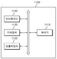
도 11을 참조하면, 본 발명의 제 5 실시예에 따른 전자시스템(1100)은 제어기(1110), 입출력 장치(1120), 기억 장치(1130), 인터페이스(1140), 및 버스 구조체(1150)을 구비할 수 있다. 상기 기억 장치(1130)는 도 1 내지 도 10을 참조하여 설명한 것과 유사한 반도체 패키지들(100, 200, 300, 400)를 구비하는 것일 수 있다. 상기 버스 구조체(1150)는 상기 제어기(1110), 상기 입출력 장치(1120), 상기 기억 장치(1130), 및 상기 인터페이스(1140) 상호 간에 데이터들이 이동하는 통로를 제공하는 역할을 할 수 있다.11, an
상기 제어기(1110)는 적어도 하나의 마이크로프로세서, 디지털 신호 프로세서, 마이크로컨트롤러, 그리고 이들과 유사한 기능을 수행할 수 있는 논리 소자들 중에서 적어도 어느 하나를 포함할 수 있다. 상기 입출력 장치(1120)는 키패드, 키보드 및 표시 장치(display device) 등에서 선택된 적어도 하나를 포함할 수 있다. 상기 기억 장치(1130)는 데이터 및/또는 제어기(1110)에 의해 실행되는 명령어 등을 저장하는 역할을 할 수 있다.The
상기 기억 장치(1130)는 디램(dynamic random access memory; DRAM), 및 에스램(static random access memory; SRAM)과 같은 휘발성 메모리 칩, 플래시메모리(flash memory), 상변화메모리(phase change memory), 엠램(magnetic random access memory; MRAM), 또는 알램(resistive random access memory; RRAM)과 같은 비휘발성 메모리 칩, 또는 이들의 조합을 구비할 수 있다. The
상기 인터페이스(1140)는 통신 네트워크로 데이터를 전송하거나 통신 네트워크로부터 데이터를 수신하는 역할을 할 수 있다. 상기 인터페이스(1140)는 유무선 형태일 수 있다. 예를 들어, 상기 인터페이스(1140)는 안테나 또는 유무선 트랜시버 등을 포함할 수 있다. 상기 전자 시스템(1100)에는 응용 칩셋(Application Chipset), 카메라 이미지 프로세서(Camera Image Processor:CIS), 그리고 입출력 장치 등이 더 제공될 수 있다.The
상기 전자 시스템(1100)은 모바일 시스템, 개인용 컴퓨터, 산업용 컴퓨터 또는 다양한 기능을 수행하는 로직 시스템 등으로 구현될 수 있다. 예컨대, 모바일 시스템은 개인 휴대용 정보 단말기(PDA; Personal Digital Assistant), 휴대용 컴퓨터, 웹 타블렛(web tablet), 모바일폰(mobile phone), 무선폰(wireless phone), 랩톱(laptop) 컴퓨터, 메모리 카드, 디지털 뮤직 시스템(digital music system) 그리고 정보 전송/수신 시스템 중 어느 하나일 수 있다. 상기 전자 시스템(1100)이 무선 통신을 수행할 수 있는 장비인 경우에, 상기 전자 시스템(1100)은 CDMA(Code Division Multiple Access), GSM(Global System for Mobile communication), NADC(North American Digital Cellular), E-TDMA(Enhanced-Time Division Multiple Access), WCDAM(Wideband Code Division Multiple Access), CDMA2000과 같은 통신 시스템에서 사용될 수 있다.The
100, 200, 300, 400 : 반도체 패키지
110, 210, 310, 410 : 기판
120, 220, 320, 420: 제 1 반도체 칩
130, 230, 330, 430: 제 2 반도체 칩
340: 제 3 반도체 칩
111, 211, 311, 411: 기판 패드들
121, 221, 321, 421: 제 1 반도체 칩의 칩 패드들
131, 231, 331, 431: 제 2 반도체 칩의 칩 패드들
341: 제 3 반도체 칩의 칩 패드들
150: 봉지재
180: 외부 단자
161: 제 1 접착층
162: 제 2 접착층
322, 332, 342, 422, 432, 442, 452: 본딩 와이어들 100, 200, 300, 400: semiconductor package
110, 210, 310, 410: substrate
120, 220, 320, 420: a first semiconductor chip
130, 230, 330, 430: a second semiconductor chip
340: Third semiconductor chip
111, 211, 311, 411: substrate pads
121, 221, 321, 421: chip pads of the first semiconductor chip
131, 231, 331, 431: chip pads of the second semiconductor chip
341: chip pads of the third semiconductor chip
150: Encapsulant
180: External terminal
161: first adhesive layer
162: second adhesive layer
322, 332, 342, 422, 432, 442, 452:
Claims (10)
상기 기판에 적층되고, 상면에 그의 길이 방향을 따라 배열된 복수의 칩 패드들을 갖는 제 1 반도체 칩; 및
상기 제 1 반도체 칩 상에 회전되어 적층되고, 상면에 그의 길이 방향을 따라 배열된 복수의 칩 패드들을 갖는 제 2 반도체 칩을 포함하되,
제1 반도체 칩의 칩 패드들은:
외부로 노출되는 적어도 하나의 노출 칩 패드; 및
상기 제2 반도체 칩에 의해 외부로 비노출되는 적어도 하나의 비노출 칩 패드를 포함하고,
상기 제2 반도체 칩의 칩 패드들은, 상기 노출 칩 패드와 전기적으로 연결되고, 상기 비 노출 칩 패드와 전기적으로 연결되지 않는 반도체 패키지.Board;
A first semiconductor chip stacked on the substrate and having a plurality of chip pads arranged on an upper surface thereof along a longitudinal direction thereof; And
And a second semiconductor chip which is rotated and laminated on the first semiconductor chip and has a plurality of chip pads arranged on its top surface along its longitudinal direction,
The chip pads of the first semiconductor chip are:
At least one exposed chip pad exposed to the outside; And
And at least one unexposed chip pad unexposed to the outside by the second semiconductor chip,
Wherein the chip pads of the second semiconductor chip are electrically connected to the exposed chip pads and are not electrically connected to the non-exposed chip pads.
상기 제 1 및 제 2 반도체 칩들의 길이 방향이 이루는 내각의 크기는 0°를 초과하고 45°이하인 반도체 패키지.The method according to claim 1,
Wherein a size of the internal angle formed by the longitudinal direction of the first and second semiconductor chips is more than 0 DEG and less than 45 DEG.
상기 제 2 반도체 칩은 상기 제 1 및 제 2 반도체 칩의 중앙을 잇는 가상의 중심축을 회전축으로 하여 회전되어 적층된 반도체 패키지. The method according to claim 1,
And the second semiconductor chip is rotated and stacked around a virtual central axis connecting the centers of the first and second semiconductor chips as a rotation axis.
상기 기판은 다수의 기판 패드들을 갖되,
상기 제 2 반도체 칩의 칩 패드들은 상기 노출 칩 패드들과 본딩 와이어(bonding wire)들에 의해 전기적으로 연결되며,
상기 노출 칩 패드들은 상기 기판 패드들과 본딩 와이어들에 의해 전기적으로 연결되는 반도체 패키지. The method according to claim 1,
The substrate has a plurality of substrate pads,
The chip pads of the second semiconductor chip are electrically connected to the exposed chip pads by bonding wires,
Wherein the exposed chip pads are electrically connected to the substrate pads by bonding wires.
상기 본딩 와이어들은 상기 제 1 반도체 칩들의 상기 노출 칩 패드들을 상기 제 2 반도체 칩의 칩 패드들과 전기적으로 연결하는 반도체 패키지. 5. The method of claim 4,
Wherein the bonding wires electrically connect the exposed chip pads of the first semiconductor chips to the chip pads of the second semiconductor chip.
상기 본딩 와이어들은 상기 노출 칩 패드들 중 하나의 장측 노출 칩 패드들을 상기 제 2 반도체 칩의 칩 패드들과 전기적으로 연결하는 반도체 패키지. 6. The method of claim 5,
Wherein the bonding wires electrically couple one of the exposed chip pads of the exposed chip pads to chip pads of the second semiconductor chip.
상기 본딩 와이어들은 상기 노출 칩패드들 중 2 개의 장측 노출 칩 패드들을 상기 제 2 반도체 칩의 칩 패드들과 전기적으로 연결하는 반도체 패키지. 6. The method of claim 5,
Wherein the bonding wires electrically couple two long-side exposed chip pads of the exposed chip pads to chip pads of the second semiconductor chip.
상기 제 2 반도체 칩에 적층되는 제 3 반도체 칩을 더 포함하되,
상기 제 3 반도체 칩은 상기 제 1 내지 제 3 반도체 칩들의 중앙 부분을 잇는 가상의 중심축을 회전축으로 하여, 상기 제 2 반도체 칩이 상기 제 1 반도체 칩에 회전하여 적층된 회전 방향과 동일한 회전 방향으로 회전되어 적층되는 반도체 패키지. The method according to claim 1,
And a third semiconductor chip stacked on the second semiconductor chip,
The third semiconductor chip has a virtual center axis connecting the central portions of the first to third semiconductor chips as a rotation axis, and the second semiconductor chip is rotated in the same rotational direction as the rotational direction in which the second semiconductor chip is rotated on the first semiconductor chip Wherein the semiconductor package is rotated and stacked.
상기 제 1 내지 제 3 반도체 칩들의 길이 방향들이 이루는 내각의 크기들은 각각 동일하며, 상기 내각의 크기는 0°를 초과하고 45°이하인 반도체 패키지.9. The method of claim 8,
The sizes of the internal angles formed by the longitudinal directions of the first to third semiconductor chips are the same, and the size of the internal angle is more than 0 DEG and less than 45 DEG.
상기 기판 상에 순차적으로 적층되는 제1 및 제2 반도체 칩들을 포함하되, 상기 제1 및 제2 반도체 칩들은 각각의 중앙을 잇는 가상의 중심축을 회전축으로 하여 회전되어 배치되고,
상기 제1 및 제2 반도체 칩들의 각각은 상면에 그의 길이 방향을 따라 배열된 복수의 칩 패드들을 갖고,
상기 제1 반도체 칩의 칩 패드들은:
외부로 노출되는 적어도 하나의 노출 칩 패드; 및
상기 제2 반도체 칩에 의해 외부로 비노출되는 적어도 하나의 비노출 칩 패드를 포함하고,
상기 제2 반도체 칩의 칩 패드들은, 상기 노출 칩 패드와 전기적으로 연결되고, 상기 비 노출 칩 패드와 전기적으로 연결되지 않는 반도체 패키지.Claims [1]
Wherein the first and second semiconductor chips are arranged so as to be rotatable about an imaginary center axis connecting the center of each of the first and second semiconductor chips,
Wherein each of the first and second semiconductor chips has a plurality of chip pads arranged on an upper surface thereof along a longitudinal direction thereof,
The chip pads of the first semiconductor chip include:
At least one exposed chip pad exposed to the outside; And
And at least one unexposed chip pad unexposed to the outside by the second semiconductor chip,
Wherein the chip pads of the second semiconductor chip are electrically connected to the exposed chip pads and are not electrically connected to the non-exposed chip pads.
Priority Applications (2)
| Application Number | Priority Date | Filing Date | Title |
|---|---|---|---|
| KR1020100063931A KR101695770B1 (en) | 2010-07-02 | 2010-07-02 | Semiconductor Package Having Spin Stacked Structure |
| US13/175,406 US8487452B2 (en) | 2010-07-02 | 2011-07-01 | Semiconductor package having a stacked structure |
Applications Claiming Priority (1)
| Application Number | Priority Date | Filing Date | Title |
|---|---|---|---|
| KR1020100063931A KR101695770B1 (en) | 2010-07-02 | 2010-07-02 | Semiconductor Package Having Spin Stacked Structure |
Publications (2)
| Publication Number | Publication Date |
|---|---|
| KR20120003200A KR20120003200A (en) | 2012-01-10 |
| KR101695770B1 true KR101695770B1 (en) | 2017-01-13 |
Family
ID=45399107
Family Applications (1)
| Application Number | Title | Priority Date | Filing Date |
|---|---|---|---|
| KR1020100063931A Active KR101695770B1 (en) | 2010-07-02 | 2010-07-02 | Semiconductor Package Having Spin Stacked Structure |
Country Status (2)
| Country | Link |
|---|---|
| US (1) | US8487452B2 (en) |
| KR (1) | KR101695770B1 (en) |
Families Citing this family (12)
| Publication number | Priority date | Publication date | Assignee | Title |
|---|---|---|---|---|
| US20130256883A1 (en) * | 2012-03-27 | 2013-10-03 | Intel Mobile Communications GmbH | Rotated semiconductor device fan-out wafer level packages and methods of manufacturing rotated semiconductor device fan-out wafer level packages |
| JP5959097B2 (en) * | 2012-07-03 | 2016-08-02 | ルネサスエレクトロニクス株式会社 | Semiconductor device |
| JP6150375B2 (en) * | 2012-12-06 | 2017-06-21 | ルネサスエレクトロニクス株式会社 | Semiconductor device |
| KR102062738B1 (en) | 2013-02-25 | 2020-01-06 | 삼성전자주식회사 | Semiconductor Package |
| JP6371582B2 (en) * | 2014-05-15 | 2018-08-08 | ローム株式会社 | package |
| KR102276477B1 (en) * | 2014-11-19 | 2021-07-13 | 에스케이하이닉스 주식회사 | Method for fabricating semiconductor package having overhang part |
| US9337146B1 (en) * | 2015-01-30 | 2016-05-10 | Qualcomm Incorporated | Three-dimensional integrated circuit stack |
| FR3054372A1 (en) * | 2016-07-21 | 2018-01-26 | St Microelectronics Tours Sas | MOUNTING ELECTRONIC COMPONENTS |
| US10985136B2 (en) | 2016-12-11 | 2021-04-20 | Intel Corporation | Microelectronic die stack having at least one rotated microelectronic die |
| KR102508552B1 (en) * | 2018-04-30 | 2023-03-10 | 에스케이하이닉스 주식회사 | Stack package including through mold vias |
| KR102573307B1 (en) * | 2018-09-28 | 2023-08-31 | 삼성전자 주식회사 | Semiconductor packages |
| CN112768443B (en) * | 2021-04-08 | 2021-06-25 | 甬矽电子(宁波)股份有限公司 | Multi-layer stacked packaging structure and preparation method of multi-layer stacked packaging structure |
Citations (3)
| Publication number | Priority date | Publication date | Assignee | Title |
|---|---|---|---|---|
| US6133637A (en) | 1997-01-24 | 2000-10-17 | Rohm Co., Ltd. | Semiconductor device having a plurality of semiconductor chips |
| US20090001574A1 (en) * | 2007-06-29 | 2009-01-01 | Fang Chun-Fu | Multi-chips Stacked package structure |
| US20090267224A1 (en) | 2008-04-29 | 2009-10-29 | Silicon Laboratories Inc. | Circuit device including rotated stacked die |
Family Cites Families (5)
| Publication number | Priority date | Publication date | Assignee | Title |
|---|---|---|---|---|
| US6930378B1 (en) | 2003-11-10 | 2005-08-16 | Amkor Technology, Inc. | Stacked semiconductor die assembly having at least one support |
| US20060267173A1 (en) | 2005-05-26 | 2006-11-30 | Sandisk Corporation | Integrated circuit package having stacked integrated circuits and method therefor |
| KR101413220B1 (en) | 2007-10-02 | 2014-06-30 | 삼성전자주식회사 | Semiconductor package having interposer and method for manufacturing semiconductor package |
| JP5405785B2 (en) * | 2008-09-19 | 2014-02-05 | ルネサスエレクトロニクス株式会社 | Semiconductor device |
| KR20100036064A (en) * | 2008-09-29 | 2010-04-07 | 에스티에스반도체통신 주식회사 | Method for manufacturing semiconductor chip stack package |
-
2010
- 2010-07-02 KR KR1020100063931A patent/KR101695770B1/en active Active
-
2011
- 2011-07-01 US US13/175,406 patent/US8487452B2/en active Active
Patent Citations (3)
| Publication number | Priority date | Publication date | Assignee | Title |
|---|---|---|---|---|
| US6133637A (en) | 1997-01-24 | 2000-10-17 | Rohm Co., Ltd. | Semiconductor device having a plurality of semiconductor chips |
| US20090001574A1 (en) * | 2007-06-29 | 2009-01-01 | Fang Chun-Fu | Multi-chips Stacked package structure |
| US20090267224A1 (en) | 2008-04-29 | 2009-10-29 | Silicon Laboratories Inc. | Circuit device including rotated stacked die |
Also Published As
| Publication number | Publication date |
|---|---|
| US20120001347A1 (en) | 2012-01-05 |
| KR20120003200A (en) | 2012-01-10 |
| US8487452B2 (en) | 2013-07-16 |
Similar Documents
| Publication | Publication Date | Title |
|---|---|---|
| KR101695770B1 (en) | Semiconductor Package Having Spin Stacked Structure | |
| US11380651B2 (en) | Semiconductor package including stacked semiconductor chips | |
| US9985002B2 (en) | Thin stack packages | |
| US10008488B2 (en) | Semiconductor module adapted to be inserted into connector of external device | |
| US9385109B2 (en) | Semiconductor packages having trench-shaped opening and methods for fabricating the same | |
| US20130277831A1 (en) | Semiconductor package and method of fabricating the same | |
| US9899361B2 (en) | Semiconductor package | |
| KR20120088013A (en) | Semiconductor Package having decoupling semiconductor capacitor | |
| US9730323B2 (en) | Semiconductor package | |
| US11309286B2 (en) | Stack packages including a hybrid wire bonding structure | |
| US10553567B2 (en) | Chip stack packages | |
| US11462511B2 (en) | Semiconductor package including stacked semiconductor chips | |
| US20200251447A1 (en) | Semiconductor packages having stacked chip structure | |
| US11227858B2 (en) | Semiconductor package including stacked semiconductor chips | |
| US11222872B2 (en) | Semiconductor package including stacked semiconductor chips | |
| KR101950976B1 (en) | Semiconductor package | |
| CN112103283B (en) | Package-on-package including support substrate | |
| US11322475B2 (en) | Stack semiconductor packages having wire-bonding connection structure | |
| US20120068350A1 (en) | Semiconductor packages, electronic devices and electronic systems employing the same | |
| US10658350B2 (en) | Semiconductor package | |
| CN111883489B (en) | Package-on-package including fan-out subpackages | |
| US11784162B2 (en) | Semiconductor package including vertical interconnector | |
| US11270958B2 (en) | Semiconductor package including capacitor | |
| CN113257787B (en) | Semiconductor package including chips stacked on a base module | |
| KR101688005B1 (en) | Semiconductor package having dual land and related device |
Legal Events
| Date | Code | Title | Description |
|---|---|---|---|
| PA0109 | Patent application |
St.27 status event code: A-0-1-A10-A12-nap-PA0109 |
|
| PG1501 | Laying open of application |
St.27 status event code: A-1-1-Q10-Q12-nap-PG1501 |
|
| R18-X000 | Changes to party contact information recorded |
St.27 status event code: A-3-3-R10-R18-oth-X000 |
|
| A201 | Request for examination | ||
| PA0201 | Request for examination |
St.27 status event code: A-1-2-D10-D11-exm-PA0201 |
|
| D13-X000 | Search requested |
St.27 status event code: A-1-2-D10-D13-srh-X000 |
|
| D14-X000 | Search report completed |
St.27 status event code: A-1-2-D10-D14-srh-X000 |
|
| R17-X000 | Change to representative recorded |
St.27 status event code: A-3-3-R10-R17-oth-X000 |
|
| P22-X000 | Classification modified |
St.27 status event code: A-2-2-P10-P22-nap-X000 |
|
| R17-X000 | Change to representative recorded |
St.27 status event code: A-3-3-R10-R17-oth-X000 |
|
| E902 | Notification of reason for refusal | ||
| PE0902 | Notice of grounds for rejection |
St.27 status event code: A-1-2-D10-D21-exm-PE0902 |
|
| P11-X000 | Amendment of application requested |
St.27 status event code: A-2-2-P10-P11-nap-X000 |
|
| P13-X000 | Application amended |
St.27 status event code: A-2-2-P10-P13-nap-X000 |
|
| E701 | Decision to grant or registration of patent right | ||
| PE0701 | Decision of registration |
St.27 status event code: A-1-2-D10-D22-exm-PE0701 |
|
| GRNT | Written decision to grant | ||
| PR0701 | Registration of establishment |
St.27 status event code: A-2-4-F10-F11-exm-PR0701 |
|
| PR1002 | Payment of registration fee |
St.27 status event code: A-2-2-U10-U11-oth-PR1002 Fee payment year number: 1 |
|
| PG1601 | Publication of registration |
St.27 status event code: A-4-4-Q10-Q13-nap-PG1601 |
|
| FPAY | Annual fee payment |
Payment date: 20191226 Year of fee payment: 4 |
|
| PR1001 | Payment of annual fee |
St.27 status event code: A-4-4-U10-U11-oth-PR1001 Fee payment year number: 4 |
|
| PR1001 | Payment of annual fee |
St.27 status event code: A-4-4-U10-U11-oth-PR1001 Fee payment year number: 5 |
|
| PR1001 | Payment of annual fee |
St.27 status event code: A-4-4-U10-U11-oth-PR1001 Fee payment year number: 6 |
|
| PR1001 | Payment of annual fee |
St.27 status event code: A-4-4-U10-U11-oth-PR1001 Fee payment year number: 7 |
|
| PR1001 | Payment of annual fee |
St.27 status event code: A-4-4-U10-U11-oth-PR1001 Fee payment year number: 8 |
|
| PR1001 | Payment of annual fee |
St.27 status event code: A-4-4-U10-U11-oth-PR1001 Fee payment year number: 9 |
|
| PR1001 | Payment of annual fee |
St.27 status event code: A-4-4-U10-U11-oth-PR1001 Fee payment year number: 10 |
|
| U11 | Full renewal or maintenance fee paid |
Free format text: ST27 STATUS EVENT CODE: A-4-4-U10-U11-OTH-PR1001 (AS PROVIDED BY THE NATIONAL OFFICE) Year of fee payment: 10 |
|
| P22-X000 | Classification modified |
St.27 status event code: A-4-4-P10-P22-nap-X000 |
|
| P22-X000 | Classification modified |
St.27 status event code: A-4-4-P10-P22-nap-X000 |