KR101667857B1 - Metal line connection for improved rram reliability, semiconductor arrangement comprising the same, and manufacture thereof - Google Patents
Metal line connection for improved rram reliability, semiconductor arrangement comprising the same, and manufacture thereof Download PDFInfo
- Publication number
- KR101667857B1 KR101667857B1 KR1020140186251A KR20140186251A KR101667857B1 KR 101667857 B1 KR101667857 B1 KR 101667857B1 KR 1020140186251 A KR1020140186251 A KR 1020140186251A KR 20140186251 A KR20140186251 A KR 20140186251A KR 101667857 B1 KR101667857 B1 KR 101667857B1
- Authority
- KR
- South Korea
- Prior art keywords
- metal interconnect
- rram
- array
- source
- interconnect layers
- Prior art date
- Legal status (The legal status is an assumption and is not a legal conclusion. Google has not performed a legal analysis and makes no representation as to the accuracy of the status listed.)
- Active
Links
Images


Classifications
-
- H—ELECTRICITY
- H10—SEMICONDUCTOR DEVICES; ELECTRIC SOLID-STATE DEVICES NOT OTHERWISE PROVIDED FOR
- H10B—ELECTRONIC MEMORY DEVICES
- H10B63/00—Resistance change memory devices, e.g. resistive RAM [ReRAM] devices
- H10B63/80—Arrangements comprising multiple bistable or multi-stable switching components of the same type on a plane parallel to the substrate, e.g. cross-point arrays
-
- G—PHYSICS
- G11—INFORMATION STORAGE
- G11C—STATIC STORES
- G11C13/00—Digital stores characterised by the use of storage elements not covered by groups G11C11/00, G11C23/00, or G11C25/00
- G11C13/0002—Digital stores characterised by the use of storage elements not covered by groups G11C11/00, G11C23/00, or G11C25/00 using resistive RAM [RRAM] elements
- G11C13/0021—Auxiliary circuits
- G11C13/0069—Writing or programming circuits or methods
-
- H—ELECTRICITY
- H10—SEMICONDUCTOR DEVICES; ELECTRIC SOLID-STATE DEVICES NOT OTHERWISE PROVIDED FOR
- H10B—ELECTRONIC MEMORY DEVICES
- H10B53/00—Ferroelectric RAM [FeRAM] devices comprising ferroelectric memory capacitors
- H10B53/40—Ferroelectric RAM [FeRAM] devices comprising ferroelectric memory capacitors characterised by the peripheral circuit region
-
- G—PHYSICS
- G11—INFORMATION STORAGE
- G11C—STATIC STORES
- G11C13/00—Digital stores characterised by the use of storage elements not covered by groups G11C11/00, G11C23/00, or G11C25/00
- G11C13/0002—Digital stores characterised by the use of storage elements not covered by groups G11C11/00, G11C23/00, or G11C25/00 using resistive RAM [RRAM] elements
- G11C13/0021—Auxiliary circuits
- G11C13/0097—Erasing, e.g. resetting, circuits or methods
-
- H—ELECTRICITY
- H10—SEMICONDUCTOR DEVICES; ELECTRIC SOLID-STATE DEVICES NOT OTHERWISE PROVIDED FOR
- H10B—ELECTRONIC MEMORY DEVICES
- H10B63/00—Resistance change memory devices, e.g. resistive RAM [ReRAM] devices
- H10B63/30—Resistance change memory devices, e.g. resistive RAM [ReRAM] devices comprising selection components having three or more electrodes, e.g. transistors
-
- H—ELECTRICITY
- H10—SEMICONDUCTOR DEVICES; ELECTRIC SOLID-STATE DEVICES NOT OTHERWISE PROVIDED FOR
- H10N—ELECTRIC SOLID-STATE DEVICES NOT OTHERWISE PROVIDED FOR
- H10N70/00—Solid-state devices having no potential barriers, and specially adapted for rectifying, amplifying, oscillating or switching
- H10N70/011—Manufacture or treatment of multistable switching devices
- H10N70/061—Shaping switching materials
- H10N70/063—Shaping switching materials by etching of pre-deposited switching material layers, e.g. lithography
-
- H—ELECTRICITY
- H10—SEMICONDUCTOR DEVICES; ELECTRIC SOLID-STATE DEVICES NOT OTHERWISE PROVIDED FOR
- H10N—ELECTRIC SOLID-STATE DEVICES NOT OTHERWISE PROVIDED FOR
- H10N70/00—Solid-state devices having no potential barriers, and specially adapted for rectifying, amplifying, oscillating or switching
- H10N70/20—Multistable switching devices, e.g. memristors
- H10N70/24—Multistable switching devices, e.g. memristors based on migration or redistribution of ionic species, e.g. anions, vacancies
-
- H—ELECTRICITY
- H10—SEMICONDUCTOR DEVICES; ELECTRIC SOLID-STATE DEVICES NOT OTHERWISE PROVIDED FOR
- H10N—ELECTRIC SOLID-STATE DEVICES NOT OTHERWISE PROVIDED FOR
- H10N70/00—Solid-state devices having no potential barriers, and specially adapted for rectifying, amplifying, oscillating or switching
- H10N70/801—Constructional details of multistable switching devices
- H10N70/821—Device geometry
- H10N70/826—Device geometry adapted for essentially vertical current flow, e.g. sandwich or pillar type devices
-
- H—ELECTRICITY
- H10—SEMICONDUCTOR DEVICES; ELECTRIC SOLID-STATE DEVICES NOT OTHERWISE PROVIDED FOR
- H10N—ELECTRIC SOLID-STATE DEVICES NOT OTHERWISE PROVIDED FOR
- H10N70/00—Solid-state devices having no potential barriers, and specially adapted for rectifying, amplifying, oscillating or switching
- H10N70/801—Constructional details of multistable switching devices
- H10N70/841—Electrodes
-
- H—ELECTRICITY
- H10—SEMICONDUCTOR DEVICES; ELECTRIC SOLID-STATE DEVICES NOT OTHERWISE PROVIDED FOR
- H10N—ELECTRIC SOLID-STATE DEVICES NOT OTHERWISE PROVIDED FOR
- H10N70/00—Solid-state devices having no potential barriers, and specially adapted for rectifying, amplifying, oscillating or switching
- H10N70/801—Constructional details of multistable switching devices
- H10N70/881—Switching materials
- H10N70/883—Oxides or nitrides
- H10N70/8833—Binary metal oxides, e.g. TaOx
-
- H10W20/43—
-
- H10W20/435—
-
- G—PHYSICS
- G11—INFORMATION STORAGE
- G11C—STATIC STORES
- G11C13/00—Digital stores characterised by the use of storage elements not covered by groups G11C11/00, G11C23/00, or G11C25/00
- G11C13/0002—Digital stores characterised by the use of storage elements not covered by groups G11C11/00, G11C23/00, or G11C25/00 using resistive RAM [RRAM] elements
- G11C13/0021—Auxiliary circuits
- G11C13/003—Cell access
-
- G—PHYSICS
- G11—INFORMATION STORAGE
- G11C—STATIC STORES
- G11C13/00—Digital stores characterised by the use of storage elements not covered by groups G11C11/00, G11C23/00, or G11C25/00
- G11C13/0002—Digital stores characterised by the use of storage elements not covered by groups G11C11/00, G11C23/00, or G11C25/00 using resistive RAM [RRAM] elements
- G11C13/0021—Auxiliary circuits
- G11C13/0069—Writing or programming circuits or methods
- G11C2013/0071—Write using write potential applied to access device gate
-
- G—PHYSICS
- G11—INFORMATION STORAGE
- G11C—STATIC STORES
- G11C2213/00—Indexing scheme relating to G11C13/00 for features not covered by this group
- G11C2213/70—Resistive array aspects
- G11C2213/79—Array wherein the access device being a transistor
-
- G—PHYSICS
- G11—INFORMATION STORAGE
- G11C—STATIC STORES
- G11C2213/00—Indexing scheme relating to G11C13/00 for features not covered by this group
- G11C2213/70—Resistive array aspects
- G11C2213/82—Array having, for accessing a cell, a word line, a bit line and a plate or source line receiving different potentials
Landscapes
- Engineering & Computer Science (AREA)
- Manufacturing & Machinery (AREA)
- Semiconductor Memories (AREA)
- Physics & Mathematics (AREA)
- Geometry (AREA)
- Condensed Matter Physics & Semiconductors (AREA)
- General Physics & Mathematics (AREA)
- Computer Hardware Design (AREA)
- Microelectronics & Electronic Packaging (AREA)
- Power Engineering (AREA)
Abstract
집적 회로 디바이스는 RRAM 셀들의 어레이, RRAM 셀들의 어레이에 대한 비트 라인들의 어레이, 및 RRAM 셀들의 어레이에 대한 소스 라인들의 어레이를 포함한다. 소스 라인들 및 비트 라인들은 RRAM 셀들 위의 금속 상호 접속층들에 있다. 이에 의해, 종래의 와이어 크기보다 큰 소스 라인들이 제공되고, 이는 대략 10배만큼 리셋 속도를 증가시킨다. 따라서, RRAM 트랜지스터들의 수명 및 RRAM 디바이스의 내구성이 유사한 정도로 개선된다.An integrated circuit device includes an array of RRAM cells, an array of bit lines for an array of RRAM cells, and an array of source lines for an array of RRAM cells. The source lines and bit lines are in the metal interconnect layers above the RRAM cells. Thereby, source lines larger than conventional wire sizes are provided, which increases the reset rate by approximately 10 times. Thus, the lifetime of the RRAM transistors and the durability of the RRAM devices are improved to a similar degree.
Description
우선권 주장 및 상호 참조Priority claim and cross-reference
본 출원은 2013년 12월 27일자에 출원된 미국 가특허 출원 제61/921,148호의 우선권을 주장한다.
This application claims priority from U.S. Provisional Patent Application No. 61 / 921,148, filed December 27, 2013.
기술 분야Technical field
본 발명개시는 저항성 랜덤 액세스 메모리를 갖는 집적 회로 디바이스, 이와 같은 디바이스를 만드는 방법, 및 이와 같은 디바이스를 동작시키는 방법에 관한 것이다.The disclosure is directed to an integrated circuit device having a resistive random access memory, a method of making such a device, and a method of operating such a device.
저항성 랜덤 액세스 메모리(resistive random access memory; RRAM)는 단순한 구조물, 낮은 동작 전압, 높은 속도, 양호한 내구성, 및 CMOS 공정 호환성을 갖는다. RRAM은 종래의 플래시 메모리에 축소형 교체를 제공하기 위한 가장 유망한 대안으로, 광 디스크 및 비휘발성 메모리 어레이와 같은 디바이스에서의 폭넓은 적용이 발견되고 있다.Resistive random access memory (RRAM) has a simple structure, low operating voltage, high speed, good durability, and CMOS process compatibility. RRAM is the most promising alternative to providing miniature replacement for conventional flash memory, and widespread application in devices such as optical disks and non-volatile memory arrays is being discovered.
RRAM 셀은 위상 변화를 겪도록 유도될 수 있는 물질층 내에 데이터를 저장한다. 위상 변화는 높은 저항 상태와 낮은 저항 상태 사이를 스위칭하기 위해 층의 일부 또는 전체 내에 유도될 수 있다. 저항 상태는 "0" 또는 "1" 중 어느 하나를 나타내는 것으로 질의 및 해석될 수 있다.An RRAM cell stores data in a layer of material that can be induced to undergo a phase change. The phase change may be induced in part or all of the layer to switch between a high resistance state and a low resistance state. The resistance state can be queried and interpreted to indicate either "0" or "1 ".
통상적인 RRAM 셀에서, 데이터 저장층은 비결정질 금속 산화물을 포함한다. 충분한 전압의 인가 시에, 금속성 브리지가 데이터 저장층에 걸쳐 형성되도록 유도되어 낮은 저항 상태를 야기한다. 금속성 브리지는 분열될 수 있고, 높은 저항 상태가 금속성 구조물의 일부 또는 전체를 녹이거나 다른 식으로 붕괴시키는 짧은 고 전류 밀도 펄스를 인가함으로써 복원된다. 데이터 저장층은 빠르게 냉각되어 낮은 저항 상태가 다시 유도될 때까지 높은 저항 상태로 남아 있다. RRAM 셀은 통상적으로 FEOL(front-end-of line) 처리 이후에 형성된다. 통상적인 설계에서, RRAM 셀의 어레이는 한 쌍의 금속 상호 접속층들 사이에 형성된다.In a typical RRAM cell, the data storage layer comprises an amorphous metal oxide. Upon application of a sufficient voltage, a metallic bridge is induced to form across the data storage layer, resulting in a low resistance state. The metallic bridge can be broken up and restored by applying a short high current density pulse which causes the high resistance state to melt or otherwise collapse some or all of the metallic structure. The data storage layer is rapidly cooled and remains in a high resistance state until the low resistance state is again induced. RRAM cells are typically formed after front-end-of-line (FEOL) processing. In a typical design, an array of RRAM cells is formed between a pair of metal interconnect layers.
본 발명의 목적은 금속 라인 커넥션, 이를 포함하는 반도체 장치, 및 이의 제조 방법을 제공하는 것이다. It is an object of the present invention to provide a metal line connection, a semiconductor device including the same, and a method of manufacturing the same.
집적 회로 디바이스는 RRAM 셀들의 어레이, RRAM 셀들의 어레이에 대한 비트 라인들의 어레이, 및 RRAM 셀들의 어레이에 대한 소스 라인들의 어레이를 포함한다. 소스 라인들 및 비트 라인들은 RRAM 셀들 위의 금속 상호 접속층들에 있다. 이에 의해, 종래의 와이어 크기보다 큰 소스 라인들이 제공되고, 이는 대략 10배만큼 리셋 속도를 증가시킨다. 따라서, RRAM 트랜지스터들의 수명 및 RRAM 디바이스의 내구성이 유사한 정도로 개선된다. An integrated circuit device includes an array of RRAM cells, an array of bit lines for an array of RRAM cells, and an array of source lines for an array of RRAM cells. The source lines and bit lines are in the metal interconnect layers above the RRAM cells. Thereby, source lines larger than conventional wire sizes are provided, which increases the reset rate by approximately 10 times. Thus, the lifetime of the RRAM transistors and the durability of the RRAM devices are improved to a similar degree.
본 발명에 따르면, 금속 라인 커넥션, 이를 포함하는 반도체 장치, 및 이의 제조 방법을 제공하는 것이 가능하다. According to the present invention, it is possible to provide a metal line connection, a semiconductor device including the same, and a method of manufacturing the same.
본 발명개시의 양태들은 첨부 도면들과 함께 아래의 상세한 설명을 읽음으로써 가장 잘 이해된다. 본 산업계에서의 표준적인 실시에 따라, 다양한 피처(feature)들은 실척도로 도시되지 않았음을 유념한다. 사실, 다양한 피처들의 치수는 설명의 명료함을 위해 임의적으로 증가되거나 또는 감소될 수 있다.
도 1은 본 발명개시의 일부 실시예들에 따라 RRAM 디바이스를 나타낸다.
도 2a 내지 도 2c는 본 발명개시의 일부 실시예들에 따라 RRAM 디바이스에 적합한 일부 예시적인 와이어 크기를 나타낸다.
도 3은 본 발명개시의 일부 실시예들 따라 RRAM 셀을 셋팅하는 방법을 나타내는 흐름도이다.
도 4는 본 발명개시의 일부 실시예들에 따라 RRAM 셀이 RRAM 셀 셋팅 프로세스를 겪을 때 RRAM 셀에 걸친 전압 및 RRAM 셀을 통한 전류를 도시하는 그래프이다.
도 5는 본 발명개시의 일부 실시예들 따라 RRAM 셀을 리셋하는 방법을 나타내는 흐름도이다.
도 6은 본 발명개시의 일부 실시예들에 따라 RRAM 셀이 RRAM 셀 리셋 프로세스를 겪을 때 RRAM 셀에 걸친 전압 및 RRAM 셀을 통한 전류를 도시하는 그래프이다.
도 7은 본 발명개시의 일부 실시예들 따라 RRAM 디바이스 제조 방법을 나타내는 흐름도이다.
도 8 내지 도 10은 본 발명개시의 일부 실시예들에 따라 RRAM 디바이스를 제조하는 다양한 중간 단계들에서의 횡단면도를 나타낸다.
도 11 내지 도 15는 본 발명개시의 일부 실시예들에 따라 RRAM 셀을 제조하는 다양한 중간 단계들에서의 횡단면도를 나타낸다.
도 16 및 도 17은 본 발명의 일부 다른 실시예들에 따라 RRAM 디바이스를 제조하는 다양한 중간 단계들에서의 횡단면도를 나타낸다.BRIEF DESCRIPTION OF THE DRAWINGS Embodiments of the present disclosure are best understood by reading the following detailed description together with the accompanying drawings. Note that according to standard practice in the industry, various features are not shown in scale. In fact, the dimensions of the various features may be increased or decreased arbitrarily for clarity of explanation.
Figure 1 shows an RRAM device in accordance with some embodiments of the present disclosure.
Figures 2A-2C illustrate some exemplary wire sizes suitable for RRAM devices in accordance with some embodiments of the present disclosure.
3 is a flow diagram illustrating a method of setting an RRAM cell according to some embodiments of the present disclosure.
4 is a graph illustrating voltage across RRAM cells and current through RRAM cells when an RRAM cell undergoes an RRAM cell setting process in accordance with some embodiments of the present disclosure.
5 is a flow diagram illustrating a method for resetting an RRAM cell in accordance with some embodiments of the present disclosure.
6 is a graph illustrating voltage across RRAM cells and current through RRAM cells when the RRAM cell undergoes an RRAM cell reset process in accordance with some embodiments of the present disclosure.
7 is a flow diagram illustrating a method of fabricating an RRAM device in accordance with some embodiments of the present disclosure.
8-10 illustrate a cross-sectional view at various intermediate stages of manufacturing an RRAM device in accordance with some embodiments of the present disclosure.
Figures 11-15 illustrate cross-sectional views at various intermediate stages of fabricating RRAM cells in accordance with some embodiments of the present disclosure.
Figures 16 and 17 illustrate cross-sectional views at various intermediate stages of manufacturing an RRAM device in accordance with some alternative embodiments of the present invention.
다음의 발명개시는 제공된 주제의 상이한 피처들을 구현하는 다수의 상이한 실시예들, 또는 예들을 제공한다. 컴포넌트 및 장치의 특정한 예들은 본 발명개시를 단순화하기 위해 이하에 설명된다. 물론, 이러한 설명은 단지 예일 뿐 제한하기 위한 것이 아니다. 예를 들어, 이어지는 설명에서 제 2 피처 위에 또는 제 2 피처 상에 제 1 피처의 형성은, 제 1 피처 및 제 2 피처가 직접 접촉하여 형성되는 실시예들을 포함할 수 있고, 제 1 피처 및 제 2 피처가 직접 접촉하지 않도록 제 1 피처와 제 2 피처 사이에 부가적인 피처들이 형성되는 실시예들을 또한 포함할 수 있다. 게다가, 본 발명개시는 다양한 예들에서 참조 번호 및/또는 문자를 반복할 수 있다. 이러한 반복은 단순함과 명료함을 위한 것으로, 그 자체가 논의된 다양한 실시예들 및/또는 구성들 사이의 관계를 지시하지 않는다.The following inventive disclosures provide a number of different embodiments, or examples, that implement different features of a given subject matter. Specific examples of components and devices are described below to simplify disclosure of the present invention. Of course, this description is for illustrative purposes only, and not for limitation. For example, in the following description, formation of a first feature on a second feature or on a second feature may include embodiments in which a first feature and a second feature are formed in direct contact, and the first feature and the second feature 2 features may be formed between the first feature and the second feature such that the second feature is not in direct contact. In addition, the disclosure of the present invention may repeat the reference numerals and / or characters in various examples. Such repetition is for simplicity and clarity and does not itself dictate the relationship between the various embodiments and / or configurations discussed.
더욱이, "아래", "밑", "하위", "위", "상위" 등과 같은 공간적 관계 용어들이 도면들에 나타난 바와 같이 다른 요소(들) 또는 피처(들)에 대한 하나의 요소 또는 피처의 관계를 설명하는데 설명의 용이함을 위해 본 명세서에서 이용될 수 있다. 공간적 관계 용어들은 도면에 도시된 방향은 물론 사용 중이거나 동작 중인 디바이스의 상이한 방향을 포함하기 위한 것이다. 장치는 다른 식으로 배향될 수 있고(90도 회전 또는 다른 방향으로 있음), 그에 맞춰 본 명세서에서 이용되는 공간적 관계 설명이 또한 이해된다.Moreover, it is to be understood that spatial relation terms such as "below", "under", "subordinate", "above", "above", etc., Can be used herein for ease of explanation. Spatial relationship terms are intended to encompass different orientations of the device being used or operating, as well as those depicted in the figures. The device can be oriented differently (with a 90 degree rotation or in a different orientation), and accordingly the spatial relationship explanations used herein are also understood.
집적 회로의 밀도가 증가함에 따라, 금속 상호 접속층에서 와이어의 저항-용량(resistance-capacitance; RC) 지연은 집적 회로 성능에 상당한 영향을 미치기 시작했다. 최신의 집적 회로(IC)는 알루미늄 대신에 구리를 이용하고 SiO2 대신에 로우-k(low-k) 유전체를 이용함으로써 금속 상호 접속층의 RC 지연을 감소시킨다. RC 지연은 또한 더욱 두꺼운 와이어를 이용하여 더욱 긴 커넥션을 만들도록 크기 조정함으로써 감소된다.As the density of integrated circuits increases, the resistance-capacitance (RC) delay of the wires in the metal interconnect layer has begun to have a significant impact on integrated circuit performance. Latest integrated circuit (IC) is to reduce the RC delay of the metal interconnect layer by using the copper in place of aluminum, and using the low -k (low-k) dielectric, instead of SiO 2. The RC delay is also reduced by scaling to make longer connections using thicker wires.
크기 조정은 금속 상호 접속층의 와이어 두께 및 폭을 변경함으로써 이루어진다. 기판에 가장 가까운 가장 낮은 금속 상호 접속층은 가장 얇고 가장 좁은 와이어를 갖는다. 가장 낮은 층의 와이어는 가장 큰 RC 지연을 갖고, 로컬 상호 접속을 만드는데 이용된다. 추가적인 금속 상호 접속층이 추가됨에 따라, 와이어 두께, 폭 및 분리는 점점 증가한다. 가장 높은 금속 상호 접속층은 가장 두껍고, 가장 넓고, 가장 넓게 이격된 와이어를 갖는다. 가장 위의 층은 가장 낮은 RC 지연을 갖고, 전력 및 클록 분배에 이용되며 글로벌 신호 라우팅에 이용된다. Scaling is achieved by changing the wire thickness and width of the metal interconnect layer. The lowest metal interconnect layer closest to the substrate has the thinnest and narrowest wire. The wire in the lowest layer has the largest RC delay and is used to make a local interconnect. As additional metal interconnect layers are added, the wire thickness, width, and separation increase. The highest metal interconnect layer has the thickest, widest, and widest spaced wire. The top layer has the lowest RC delay, is used for power and clock distribution, and is used for global signal routing.
최신의 집적 회로는 통상적으로 복잡한 상호 관계를 갖는 수천 개의 컴포넌트를 포함한다. 이러한 복잡성으로 인해, 금속 상호 접속층에서 와이어의 배치 및 라우팅은 일반적으로 전자 설계 자동화(electronic design automation; EDA)의 프로세스에서 컴퓨터에 의해 결정된다. 통상적으로, 매우 많은 수의 상이한 회로 설계가 EDA 프로그램에 제공된 기능적 사양을 충족할 수 있다. 기본 설계 제약 외에도, 성능, 전력, 신호 무결성, 신뢰성 및 수율과 같은 문제에 관련된 다양한 상이한 성능 목표가 존재한다. 제약 및 목표 기능을 평가는 다수의 가능성 및 계산적 요구 사항으로 인해, 최적 설계를 지정하는 문제는 수학적으로 아주 다루기 어렵다. 수학적 난제는 최적이 존재하지만 실현 가능한 시간 기간 내에 알아낼 수 없다는 것을 의미한다. 따라서, EDA가 최적의 해결책을 찾지만, 해결책에 대한 검색은 실제적인 제한 시간 내에 도달하도록 해결책에 대한 설계 규칙에 의해 제한되어야 한다.Modern integrated circuits typically include thousands of components with complex interrelationships. Because of this complexity, the placement and routing of wires in metal interconnect layers is typically determined by the computer in the process of electronic design automation (EDA). Typically, a very large number of different circuit designs can meet the functional specifications provided in the EDA program. In addition to the basic design constraints, there are a variety of different performance goals related to problems such as performance, power, signal integrity, reliability and yield. Due to the large number of possibilities and computational requirements for evaluating constraint and target functions, the problem of specifying the optimal design is mathematically very difficult to handle. Mathematical difficulties mean that there is an optimum but can not be found within a realizable time period. Thus, while EDA finds an optimal solution, the search for a solution should be limited by the design rules for the solution to arrive within a practical time limit.
RRAM 셀마다 하나의 트랜지스터를 제공하는 1T1R 아키텍처를 갖는 RRAM 디바이스의 내구성은 대개 트랜지스터의 수명에 의해 제한되는 것이 결정되었다. 트랜지스터는 리셋 동작 동안에 주로 노화된다는 것이 또한 결정되었다. 몸체 효과로 인해, 리셋 동작은 셋팅 동작보다 트랜지스터 게이트 상에 상당히 높은 전압을 요구한다. 소스 라인의 시트 저항을 감소시키는 것은 리셋 속도에 대단히 큰 증가를 제공한다는 것이 발견되었다. 예를 들어, 제 2 금속 상호 접속층(M2)에서의 와이어의 크기인 종래의 와이어 크기로부터, 제 6 금속 상호 접속층(M6)에서의 와이어의 크기로, 소스 라인을 증가시킴으로써, 리셋 동작에 요구되는 시간은 대략 10배만큼 감소될 수 있다. 결과적으로, RRAM 트랜지스터의 수명 및 RRAM 디바이스의 내구성은 대략 10배만큼 증가될 수 있다.It has been determined that the durability of RRAM devices with a 1T1R architecture providing one transistor per RRAM cell is usually limited by the lifetime of the transistor. It has also been determined that the transistor ages predominantly during the reset operation. Due to the body effect, the reset operation requires a significantly higher voltage on the transistor gate than the setting operation. It has been found that reducing the sheet resistance of the source line provides a very large increase in the reset speed. For example, by increasing the source line from the conventional wire size, which is the size of the wire in the second metal interconnect layer M2, to the size of the wire in the sixth metal interconnect layer M6, The required time can be reduced by about 10 times. As a result, the lifetime of the RRAM transistor and the durability of the RRAM device can be increased by approximately 10 times.
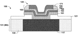
도 1은 본 발명개시의 일부 실시예들에 따라 집적 회로 디바이스(100)의 예시를 제공한다. 집적 회로 디바이스(100)는 반도체 기판(101) 및 기판(101) 위에 형성된 복수의 금속 상호 접속층들(131)(M1 내지 M6)을 포함한다. RRAM 셀(125)은 이러한 금속 상호 접속층들(131) 중 하나에, 이러한 금속 상호 접속층들 중 2개의 상호 접속층들 사이에, 또는 상위 층에 형성될 수 있다. 대부분의 실시예들에서, RRAM 셀(125)은 열 예산에 대한 제약을 충족시키기 위해 제 4 (M4) 금속 상호 접속층(131) 위에 형성된다. 일부 실시예들에서, RRAM 셀(125)은 도 1에 도시된 바와 같이 제 4 (M4) 상호 접속층(131)과 제 5(M5) 상호 접속층(131) 사이에 형성된다.Figure 1 provides an illustration of an
RRAM 셀(125)은 메모리 블록을 형성하는 RRAM 셀들(125)의 어레이의 하나이다. 메모리 블록에서 RRAM 셀(125)을 어드레싱하기 위한 비트 라인(133)이 RRAM 셀(125) 위의 금속 상호 접속층(131)에 형성된다. 도 1의 실시예에서, 비트 라인(133)은 제 5 (M5) 금속 상호 접속층(131)에 형성된다. 대부분의 실시예들에서, 비트 라인(133)은 비아(129)에 의해 RRAM 셀(125)의 상부 전극(127)에 접속된다.
RRAM 셀(125)을 선택하기 위한 스위칭 디바이스가 기판(101) 상에 형성된다. 도 1의 실시예에서, 스위칭 디바이스는 트랜지스터(105)이다. 이것은 1T1R 아키텍처를 갖는 실시예를 나타낸다. 일부 실시예들에서, 스위칭 디바이스는 다이오드이고, 아키텍처는 ID1R이다. 일부 실시예들에서, 스위칭 디바이스는 양극성 접합 트랜지스터이고, 아키텍처는 1BJT1R이다. 일부 실시예들에서, 스위칭 디바이스는 양극성 스위치이고, 아키텍처는 IS1R이다. A switching device for selecting the
도 1의 실시예에서, 트랜지스터(105)는 분리 영역(103)에 의해 분리된 트랜지스터들(105)의 어레이의 하나이다. 트랜지스터(105)는 소스 영역(107), 드레인 영역(113), 게이트(111), 및 게이트 유전체(109)를 포함한다. 드레인 영역(113)은 콘택 플러그(115), 제 1 내지 제 4 (M1 내지 M4) 금속 상호 접속층들(131)에 형성된 비아들(119), 및 이러한 금속 상호 접속층들(131) 사이에 형성된 비아들(117)을 통해 RRAM 셀(125)의 하부 전극(123)에 접속된다. 트랜지스터(105)를 스위칭하기 위한 워드 라인(135)이 제 3 (M3) 금속 상호 접속층(131)에 형성된다.In the embodiment of FIG. 1,
소스 라인(137)이 RRAM 셀(125)을 리셋하기 위해 전류 펄스를 공급한다. 디바이스(100)에서, 소스 라인(137)은 콘택 플러그(145), 제 1 내지 제 5 (M1 내지 M5) 금속 상호 접속층들(131)에 형성된 비아들(143), 및 이러한 금속 상호 접속층들(131) 사이에 형성된 비아들(141)을 통해 소스 영역(107)에 접속된다. 종래의 설계 규칙에 의해, 소스 라인(137)은 제 2 (M2) 금속 상호 접속층(131)에 위치하고, 비트 라인(133)보다 낮은 단면적을 갖는다. 본 발명개시의 일부 실시예들에 따라, 소스 라인(137)은 비트 라인(133)의 단면적보다 크거나 같은 단면적을 갖는다. 대부분의 실시예들에서, 소스 라인(137)은 비트 라인(133)의 단면적보다 큰 단면적을 갖는다. 대부분의 실시예들에서, 소스 라인(137)은 RRAM 셀(125) 위의 금속 상호 접속층(131)에 형성된다. 대부분의 실시예들에서, 소스 라인(137)은 비트 라인(133)이 형성된 금속 상호 접속층(131) 위의 금속 상호 접속층(131)에 형성된다. 도 1의 실시예에서, 소스 라인(137)은 제 6 (M6) 금속 상호 접속층(131)에 형성된다.A
대부분의 실시예들에서, 금속 상호 접속층(131)은 크기 조정된 장치에 있다. 크기 조정된 장치에서, 각각의 금속 상호 접속층(131) 내의 전도성 라인의 평균, 최빈, 또는 최대 단면적은 기판(101) 위에서 높이가 증가함에 따라 증가한다. 전도성 라인 폭은 일반적으로 금속 상호 접속층(131) 내에서 균일하고, 이에 의해 대부분의 실시예들에서, 특정한 금속 상호 접속층(131) 내의 전도성 라인에 대한 평균, 최빈, 또는 최대 단면적은 대략 모두 동일하다.In most embodiments, the
일부 실시예들에서, 일부 인접한 금속 상호 접속층들(131)의 전도성 라인의 평균, 최빈, 또는 최대 단면적은 동일할 수 있다. 대부분의 실시예들에서, 일부 금속 상호 접속층들(131)의 전도성 라인의 평균, 최빈, 또는 최대 단면적은 다른 금속 상호 접속층(들131)의 것보다 크고, 평균, 최빈, 또는 최대 단면적에 대해 더욱 큰 값을 갖는 금속 상호 접속층(131)은 작은 값을 갖는 금속 상호 접속층 위에 있다. 일부 실시예들에서, 전도성 라인은 횡단면도에서 대략 직사각형이어서, 이에 의해 단면적은 두께 및 폭의 곱이다. 두께는 기판(101)에 수직인, 또는 실질적으로 수직인 치수를 나타낸다. 폭은 기판(101)에 평행한, 또는 실질적으로 평행한 치수를 나타내고, 일부 실시예들에서, 길이는 전도성 라인으로 언급되는 구조물에서 폭보다 훨씬 크다는 점에서, 폭은 길이와 구별된다. 단면적의 증가는 폭의 증가, 두께의 증가, 또는 이들 양자 모두의 증가를 통해 실현될 수 있다. 대부분의 실시예들에서, 시트 저항은 대략 단면적에 반비례한다.In some embodiments, the average, mode, or maximum cross-sectional area of the conductive lines of some adjacent metal interconnect layers 131 may be the same. In most embodiments, the average, mode, or maximum cross-sectional area of the conductive lines of some metal interconnect layers 131 is greater than that of the other metal interconnect layer (s) 131, and the average, The
도 2a 내지 도 2c는 본 발명개시의 일부 실시예들에 따라 전도성 라인(153, 155, 및 157)을 나타낸다. 전도성 라인(153, 155, 및 157)은 각각 폭(153W, 155W, 및 157W) 및 두께(153T, 155T, 및 157T)를 갖는다. 일부 실시예들에서, 전도성 라인(153)은 제 2 (M2) 금속 상호 접속층(131)에 형성된다. 종래 기술의 EDA 프로그램은 M2에 소스 라인을 배치할 것으로 예상된다. 일부 실시예들에서, 전도성 라인(153)은 제 3 (M3) 금속 상호 접속층(131)에 형성된다. 일부 실시예들에서, 전도성 라인(153)은 워드 라인(word line; WL)(135)이다. 일부 실시예들에서, 전도성 라인(155)은 제 5 (M5) 금속 상호 접속층(131)에 형성된다. 일부 실시예들에서, 전도성 라인(155)은 비트 라인(bit line; BL)(133)이다. 일부 실시예들에서, 전도성 라인(157)은 제 6 (M6) 금속 상호 접속층(131)에 형성된다. 일부 실시예들에서, 전도성 라인(157)은 소스 라인(source line; SL)(137)이다. 다음 표는 본 발명개시의 일부 실시예들에 따라 이러한 전도성 라인들의 상대 치수 및 단면적에 대한 범위를 제공한다.2A-2C illustrate
본 발명개시의 일부 실시예들에 따라, 제 4 (M4) 금속 상호 접속층(131) 위에 소스 라인(137)의 배치는, 종래 설계 규칙에 따라 구성되거나 배치되는 소스 라인(137)의 단면적 및 시트 저항과 비교하면, 2개 이상의 요인에 의해 그 단면적을 증가시키고 그 시트 저항을 감소시킨다. 일부 실시예들에서, 소스 라인(137)의 단면적은 비트 라인(133)의 단면적과 동일하다. 대부분의 실시예들에서, 소스 라인(137)의 단면적은 비트 라인(133)의 단면적보다 크다. 일부 실시예들에서, 비트 라인(133) 및 RRAM 셀(125)은 소스 라인(137) 및 워드 라인(135)을 포함하는 금속 상호 접속층들(131) 사이에 위치하는 층들에 위치하거나 형성된다. 대부분의 실시예들에서, 워드 라인(135)은 비트 라인(133) 및 RRAM 셀(125) 밑에 위치한다.The placement of the
비트 라인(133), 워드 라인(135) 및 소스 라인(137)은 RRAM 셀(125)을 셋팅 및 리셋하는데 이용된다. 도 3은 RRAM 셀(125)을 세팅하기 위한 프로세스(300)의 예를 제공한다. 프로세스(300)는 통상적으로 접지인 기준 전압으로 소스 라인(137)을 세팅하는 액션(301), 트랜지스터(105)를 턴온시키기 위해 충분한 바이어스로 워드 라인(135)을 세팅하는 액션(303), 및 도 4에 도시된 바와 같이 전압-전류 사이클을 제공하기 위해 비트 라인(133)을 펄싱하는 액션(305)을 포함한다. 대부분의 실시예들에서, 1.4 V의 바이어스는 셋팅 동작(300) 동안 트랜지스터(105)를 턴온시키기에 충분하다.The
도 5는 RRAM 셀(125)을 리세하기 위한 프로세스(310)의 예를 제공한다. 프로세스(310)는 통상적으로 접지인 기준 전압으로 비트 라인(133)을 세팅하는 액션(311), 트랜지스터(105)를 턴온시키기 위해 충분한 바이어스로 워드 라인(135)을 세팅하는 액션(313), 및 도 6에 도시된 바와 같이 전압-전류 사이클을 제공하기 위해 소스 라인(137)을 펄싱하는 액션(315)을 포함한다. 대부분의 실시예들에서, 2 V이상, 예컨대, 2.4 V의 바이어스가 리셋 동작(310)동안 트랜지스터(105)를 턴온시키기 위해 요구된다. 도 4 및 도 6에 도시된 바와 같이, 리셋 동작(310)은 셋팅 동작(300)보다 높은 진폭 펄스를 요구한다. 도시된 전압은 셀(125)에 걸친 전압이다. 액션(303 및 313)은 다소 높은 전압으로 비트 라인(133) 또는 소스 라인(137)을 펄싱하여 이러한 라인들의 기생 저항을 극복한다. 비트 라인(133)보다 낮은 시트 저항을 소스 라인(137)에 제공하는 것은, 셋팅 동작 및 리셋 동작의 펄스 요구 사항을 거의 동일하게 만든다.FIG. 5 provides an example of a
도 7은 RRAM 셀(125)을 형성하는 프로세스(200)의 흐름도를 제공하고, 이는 본 발명개시의 다른 실시에에 따른 예이다. 프로세스(200)는 본 발명개시의 일부 실시예들에 따라 RRAM 디바이스(100)를 형성할 수 있다. 도 8 내지 도 10, 및 도 16 및 도 17은 본 발명개시의 일부 실시예들에 따라, 이의 중간 제조 단계에서의 RRAM 디바이스(100)를 나타낸다. 도 11 내지 도 15는 본 발명개시의 일부 실시예들에 따라, 도 16에서 식별된 영역(126) 내에 구조물 및 RRAM 셀(125)을 형성하는 다양한 단계들의 횡단면도를 나타낸다.FIG. 7 provides a flow diagram of a
프로세스(200)는 FEOL(front-end-of-line) 처리(210)로 시작한다. FEOL 처리(210)는 RRAM 셀(125)을 선택하기 위해 스위칭 디바이스를 형성하는 액션을 포함할 수 있다. 도 7의 예에서, FEOL 처리(210)는 기판(101)에 분리 영역(103)을 형성하는 액션(211), 기판(101) 상에 트랜지스터(105)를 형성하는 액션(213), 트랜지스터(105)의 소스 영역(107) 및 드레인 영역(113)을 살리시드하는 액션(215), 및 소스 콘택(145) 및 드레인 콘택(115)을 형성하는 액션(217)을 포함한다. 도 8은 FEOL 처리(210) 바로 다음의 디바이스(100)를 나타낸다.The
프로세스(200)는 디바이스(100)에 도 9에 도시된 바와 같은 제 1 내지 제 4 (M1 내지 M4) 금속 상호 접속층들(131)을 형성하는 액션(220)으로 계속된다. 액션(220)은 워드 라인(135)을 형성하는 액션(221)을 포함한다. 대부분의 실시예들에서, 워드 라인(135)은 제 1 (M3) 내지 제 3 (M3) 금속 상호 접속층들(131) 중 하나에 형성된다. 일부 실시예들에서, 워드 라인(135)은 도 9에 도시된 바와 같이 제 3 (M3) 금속 상호 접속층(131)에 형성된다.The
금속 상호 접속층(131)은 유전체(139)의 매트릭스에 전도성 라인 및 비아를 포함한다. 전도성 라인 및 비아는 임의의 전도성 물질로 형성될 수 있다. 일부 실시예들에서, 전도성 물질은 제 1 (M1) 금속 상호 접속층 위의 모든 금속 상호 접속층에 대해 구리일 수 있다. 유전체(139)는 임의의 적합한 유전체일 수 있고, 상이한 유전체들의 다수의 층들을 포함할 수 있다. 대부분의 실시예들에서, 유전체(139)는 로우-k 유전체이다. 일부 실시예들에서, 유전체(139)는 익스트림 로우-k 유전체이다. 익스트림 로우-k 유전체는 대략 2.1 이하의 유전 상수를 갖는 물질이다. 익스트림 로우-k 유전체는 일반적으로 20 % 이상의 공동(구멍 또는 에어 갭)을 갖는 낮은 유전체 물질로 형성된다. 대부분의 실시예들에서, 유전체 에칭 정지층(121)이 제 1 (M1) 내지 제 4 (M4) 금속 상호 접속층들(131) 각각 위에 형성된다. 대부분의 실시예들에서, 금속 상호 접속층(131)은 다마신 공정 또는 이중 다마신 공정으로 형성된다.The
프로세스(200)는 RRAM 셀(125)을 형성하는 일련의 액션들(230)로 계속된다. 이러한 액션들 중 제 1 액션은 홀(124)을 형성하는 것이고, 이러한 홀을 통해 RRAM 셀(125)은 도 10 및 도 11에 도시된 바와 같이, 밑에 있는 금속 상호 접속층(131)의 비아(119)와의 접촉을 형성할 수 있다. 홀(124)은 도면들에 도시된 바와 같이, 유전체(139)를 통해 또는 단지 에칭 정지층(121)을 통해 형성될 수 있다.The
일련의 액션들(230)은 RRAM 스택(160)을 형성하는 액션(233)으로 계속되고, RRAM 스택(160)에서 RRAM 셀(125)이 형성된다. 일부 실시예들에서, 액션(233) 전에, 홀(124)은 하부 전극 비아를 만들기 위해 전도성 물질로 충전된다. 다른 실시예들에서, RRAM 스택(160)은 홀(124) 위에 형성되어 도 12에 도시된 바와 같이 홀(124)을 충전한다. 대부분의 실시예들에서, RRAM 스택(160)은 도 12에 도시된 바와 같이, 확산 장벽층(161), 하부 전극층(163), RRAM 유전체층(165), 캡핑층(167), 및 상부 전극층(169)을 포함한다. 이러한 층들의 순서는 비트 라인(133)이 상부 전극층(169)에 결합되는 경우에 대한 것이다. 캡핑층(167)이 포함되는 경우, 비트 라인은 캡핑층(167)과 같은 측면의 RRAM 유전체층(165)에 결합되는 어드레싱 라인으로 식별될 수 있다. A series of
확산 장벽층(161)은 선택적 층이다. 이것은 비아(119)와 같은 하부 콘택으로부터의 물질에 의한 하부 전극층(163)의 오염을 방지하기 위해 포함될 수 있다. 확산 장벽층(161)이 포함되는 일부 실시예들에서, 하부 콘택은 구리이고, 하부 전극(163)은 구리에 의한 오염에 민감한 물질이다. 이러한 실시예들 중 일부에서, 하부 전극층(163)은 TiN이다. 확산 장벽층(161)은 임의의 적합한 조성을 가질 수 있고, 임의의 적합한 프로세스로 형성될 수 있다. 대부분의 실시예들에서, 확산 장벽층(161)은 Al, Mn, Co, Ti, Ta, W, Ni, Sn, Mg로 구성된 그룹으로부터 선택된 금속의 전도성 산화물, 질화물, 또는 산화질화물이다. 일부 실시예들에서, 확산 장벽층(161)은 TaN이다. 확산 장벽층(161)은 임의의 적합한 두께를 가질 수 있다. 적합한 두께는 과도한 저항을 일으킬 정도로 크지 않으면서 효과적인 확산 장벽을 제공하기에 충분히 크다. 대부분의 실시예들에서, 확산 장벽층(161)의 두께는 20 Å 내지 300 Å의 범위에 있다. 일부 실시예들에서, 확산 장벽층(161)의 두께는 100 Å 내지 300 Å의 범위에 있고, 예를 들어, 200 Å이다.The
하부 전극층(163)은 임의의 적합한 조성을 가질 수 있고, 임의의 적합한 프로세스로 형성될 수 있다. 적합한 조성의 예에는, 제한 없이, 금속, 금속 질화물, 및 도핑된 폴리실리콘을 포함한다. 일부 실시예들에서, 하부 전극층(163)은 금속이다. 금속은, 예를 들어, Al, Ti, Ta, Au, Pt, W, Ni, Ir, 또는 Cu일 수 있다. 일부 실시예들에서, 하부 전극층(163)은 금속 질화물이다. 금속 질화물은, 예를 들어, TaN일 수 있다. 일부 실시예들에서, 하부 전극층(163)은 도핑된 폴리실리콘이다. 도핑된 폴리실리콘은 p+ 도핑된 폴리실리콘 또는 n+ 도핑된 폴리실리콘 중 어느 하나일 수 있다. 대부분의 실시예들에서, 하부 전극층(163)의 두께는 20 Å 내지 200 Å의 범위에 있다. 일부 실시예들에서, 하부 전극층(163)의 두께는 50 Å 내지 150 Å의 범위에 있고, 예를 들어, 100 Å이다.The
RRAM 유전체(165)는 RRAM 셀의 데이터 저장층에 적합한 임의의 물질일 수 있다. RRAM 셀의 데이터 저장층에 적합한 물질은 높은 저항 상태와 낮은 저항 상태 사이에서 가역적 위상 변화를 겪도록 유도될 수 있는 물질이다. 일부 실시예들에서, 위상 변화는 비결정질 상태와 금속성 상태 사이이다. 위상 변화는 화학적 조성의 변화와 연관되거나 이러한 변화에 동반될 수 있다. 예를 들어, 비결정질 금속 산화물은 금속성 상태로 위상 변화를 겪을 때 산소를 잃을 수 있다. 이 산소는 비결정질 상태로 남아 있는 RRAM 유전체(165)의 일부분에 또는 인접한 층에 저장될 수 있다. 유전체로서 설명되었지만, 오직 낮은 저항 상태만이 유전체에 있어야 한다. 대부분의 실시예들에서, RRAM 유전체(165)는 낮은 저항 상태 동안 하이-k 유전체이다. 일부 실시예들에서, RRAM 유전체(165)는 전이 금속 산화물이다. RRAM 유전체(165)에 적합할 수 있는 물질들의 예에는, NiOX, TayOX, TiOX, HfOX, TayOX, WOX, ZrOX, AlyOX, 및 SrTiOX를 포함한다. 대부분의 실시예들에서, RRAM 유전체(165)의 두께는 20 Å 내지 100 Å의 범위에 있다. 일부 실시예들에서, RRAM 유전체(165)의 두께는 30 Å 내지 70 Å의 범위에 있고, 예를 들어, 50 Å이다.The RRAM dielectric 165 may be any material suitable for the data storage layer of the RRAM cell. A material suitable for the data storage layer of an RRAM cell is a material that can be induced to undergo a reversible phase change between a high resistance state and a low resistance state. In some embodiments, the phase change is between an amorphous state and a metallic state. The phase change may be associated with or accompanied by a change in the chemical composition. For example, amorphous metal oxides can lose oxygen when experiencing a phase change to a metallic state. This oxygen may be stored in a portion of the
캡핑층(167)은 선택적이다. 일부 실시예들에서, 캡핑층(167)은 RRAM 유전체(165) 내의 위상 변화를 용이하게 하는 산소 저장 기능을 제공한다. 일부 실시예들에서, 캡핑층(167)은 산소 농도가 비교적 낮은 금속 산화물 또는 금속이다. 캡핑층(167)에 적합할 수 있는 금속의 예에는, Ti, Hf, Pt 및 Al을 포함한다. 캡핑층(167)에 적합할 수 있는 금속 산화물의 예에는, TiOX, HfOX, ZrOX, GeOX, CeOX을 포함한다. 캡핑층(167)은 임의의 적합한 두께를 가질 수 있다. 대부분의 실시예들에서, 캡핑층(167)의 두께는 20 Å 내지 100 Å의 범위에 있다. 일부 실시예들에서, 캡핑층(167)의 두께는 30 Å 내지 70 Å의 범위에 있고, 예를 들어, 50 Å이다. 캡핑층(167)이 제공되는 경우, 캡핑층(167)은 비트 라인(133)이 접속되는 측과 같은 측의 RRAM 유전체(165) 상에 있다.The
상부 전극층(169)은 하부 전극층(163)에 적합한 것으로 식별된 조성들 중 임의의 조성을 가질 수 있다. 상부 전극층(169)은 임의의 적합한 두께를 가질 수 있다. 대부분의 실시예들에서, 상부 전극층(169)은 100 Å 내지 400 Å의 범위의 두께를 갖는다. 통상적인 실시예들에서, 상부 전극층(169)은 150 Å 내지 300 Å의 범위의 두께를 갖고, 예를 들어, 250 Å의 두께를 갖는다.The
RRAM 셀(125)을 형성하는 일련의 액션들(230)은, 도 13에 도시된 바와 같이, 상부 전극층(169)을 패턴화하는 액션(235), 및 스페이서(171)를 형성하는 액션(237)으로 계속될 수 있다. 대부분의 실시예들에서, 상부 전극층(169)을 패턴화하는 액션(235)은, 캡핑층(167)을 관통하여 계속되는 에칭을 포함한다. 대부분의 실시예들에서, RRAM 유전체(165)는 상부 전극층(169)을 패턴화하는 것에 에칭 정지를 제공한다. 스페이서(171)를 형성하는 액션(237)은 스페이서(171)를 형성하기 위해, 스페이서 물질층을 퇴적하는 것과, 에칭하는 것을 포함한다. 스페이서(171)는 임의의 적합한 스페이서 물질로 형성될 수 있다. 스페이서(171)에 적합한 물질의 예에는, 제한 없이, SiN, SiON 및 SiO2를 포함한다.The series of
일련의 액션들(230)은 액션(239)으로 계속되고, 액션(239)은 도 14에 도시된 바와 같은 구조물을 형성하기 위해 하부 전극층(163)을 패턴화하는 것이다. 도 14에 도시된 바와 같이, 하부 전극층(163)의 패턴화는 캡핑층(161)의 패턴화를 포함할 수 있다.A series of
프로세스(200)는 도 15 및 도 16에 도시된 바와 같은 구조물을 형성하기 위해 상부 전극 비아(129)를 형성하는 액션(240)으로 계속된다. 대부분의 실시예들에서, 상부 전극 비아(129)를 형성하는 것은, 유전체층(139)을 형성하는 것, 상부 전극 비아(129)를 위해 유전체층(139)을 통해 홀을 패턴화하는 것, 및 도 15 및 도 16에 도시된 바와 같은 상부 전극 비아(129)를 형성하기 위해 금속으로 홀을 충전하는 것을 포함한다.The
프로세스(200)는 도 17에 도시된 바와 같은 구조물을 형성하기 위해 제 5 (M5) 금속 상호 접속층(131)을 형성하는 액션(250)으로 계속된다. 이 예에서, 제 5 (M5) 금속 상호 접속층(131)을 형성하는 것은, 비트 라인(133)을 형성하는 액션(251)을 포함한다. 프로세스(200)의 이 순서는 RRAM 셀(125) 위에 비트 라인(133)을 배치한다.The
프로세스(200)는 도 1에 도시된 바와 같은 구조물을 형성하기 위해 제 6 (M6) 금속 상호 접속층(131)을 형성하는 액션(260)으로 계속된다. 이 예에서, 제 6 (M6) 금속 상호 접속층(131)을 형성하는 것은, 소스 라인(137)을 형성하는 액션(261)을 포함한다. 프로세스(200)의 이 순서는 RRAM 셀(125) 위에 그리고 비트 라인(133) 위에 소스 라인(137)을 배치한다. 금속 상호 접속층(131)의 종래의 스케일링으로, 이것은 RRAM 셀(125) 이전에 형성된 소스 라인의 단면적보다 크고, 비트 라인(133)의 단면적보다 큰 소스 라인(137)의 단면적을 만든다. The
본 발명개시의 일 실시예는 집적 회로 디바이스로서, 집적 회로 디바이스는 RRAM 셀들의 어레이, 어레이의 RRAM 셀들에 접속된 비트 라인들의 어레이, 및 어레이의 RRAM 셀들을 위한 소스 라인들의 어레이를 포함한다. 소스 라인들 및 비트 라인들은 RRAM 셀들을 셋팅 및 리셋하기 위해 전류를 운반하도록 구성된다. 소스 라인들은 비트 라인들보다 큰 단면적을 갖는다.One embodiment of the present disclosure is an integrated circuit device, which includes an array of RRAM cells, an array of bit lines connected to the RRAM cells of the array, and an array of source lines for the RRAM cells of the array. Source lines and bit lines are configured to carry current to set and reset RRAM cells. The source lines have a larger cross-sectional area than the bit lines.
본 발명개시의 다른 실시예는 집적 회로 디바이스로서, 집적 회로 디바이스는 반도체 기판, 반도체 기판 위에 형성된 복수의 금속 상호 접속층들, 복수의 금속 상호 접속층들 중 2개의 금속 상호 접속층들 사이에 위치하는 RRAM 셀, RRAM 셀에 결합된 비트 라이, 및 RRAM 셀에 선택적으로 결합되도록 구성된 소스 라인을 포함한다. 소스 라인 및 비트 라인 양자 모두는 반도체 기판 위에서 RRAM 셀보다 더욱 높은 금속 상호 접속층에 위치한다.Another embodiment of the present disclosure is an integrated circuit device comprising a semiconductor substrate, a plurality of metal interconnect layers formed over the semiconductor substrate, a plurality of metal interconnect layers disposed between the two metal interconnect layers, A bit line coupled to the RRAM cell, and a source line configured to be selectively coupled to the RRAM cell. Both the source line and the bit line are located on a metal interconnect layer higher than the RRAM cell on the semiconductor substrate.
본 발명개시의 다른 실시예는 RRAM 셀을 리셋하는 방법이다. 방법은, RRAM 셀의 상부 전극을 비트 라인에 결합하는 단계, RRAM 셀의 하부 전극을 비트 라인보다 낮은 시트 저항을 갖는 소스 라인에 결합하는 단계, 및 RRAM 셀을 통해 전류 펄스를 보내기 위해 소스 라인의 전압을 구동하는 단계를 포함한다. 전류 펄스는 RRAM 셀을 리셋한다. Another embodiment of the disclosure of the present invention is a method of resetting an RRAM cell. The method includes coupling an upper electrode of the RRAM cell to a bit line, coupling a lower electrode of the RRAM cell to a source line having a lower sheet resistance than the bit line, And driving the voltage. The current pulse resets the RRAM cell.
본 발명개시의 다른 실시예는 RRAM 셀을 갖는 집적 회로 디바이스를 작동하는 방법이다. RRAM 셀은 상부 전극 및 하부 전극 및 높은 저항 상태 및 낮은 저항 상태를 갖는다. 방법은 RRAM 셀을 높은 저항 상태로 셋팅하는 단계, 및 RRAM 셀을 낮은 저항 상태로 리셋하는 단계를 포함한다. RRAM 셀을 낮은 저항 상태로 리셋하는 단계는, RRAM 셀의 하부 전극을 소스 라인을 통해 소스 전위에 접속시키고, RRAM 셀의 상부 전극을 비트 라인을 통해 기준 전위에 접속시키는 단계를 포함한다. 소스 라인은 비트 라인보다 큰 단면적을 갖는다.Another embodiment of the disclosure of the present invention is a method of operating an integrated circuit device having an RRAM cell. The RRAM cell has upper and lower electrodes and a high resistance state and a low resistance state. The method includes setting the RRAM cell to a high resistance state, and resetting the RRAM cell to a low resistance state. Resetting the RRAM cell to a low resistance state includes connecting the lower electrode of the RRAM cell to the source potential through the source line and connecting the upper electrode of the RRAM cell to the reference potential through the bit line. The source line has a larger cross-sectional area than the bit line.
본 발명개시의 다른 실시예는 집적 회로 디바이스를 제조하는 방법이다. 방법은 FEOL(front-end-of-line) 처리를 통해 반도체 기판을 놓는 단계, 기판 위에 제 1 세트의 금속 상호 접속층들을 형성하는 단계, 제 1 세트의 금속 상호 접속층들 위에 RRAM 셀을 형성하는 단계, 및 제 1 세트의 금속 상호 접속층들 및 RRAM 셀 위에 제 2 세트의 금속 상호 접속층들을 형성하는 단계를 포함한다. 제 2 세트의 금속 상호 접속층들을 형성하는 단계는, RRAM 셀을 셋팅 및 리셋하기 위해 비트 라인 및 소스 라인을 형성하는 단계를 포함한다.Another embodiment of the disclosure of the present invention is a method of manufacturing an integrated circuit device. The method includes laying a semiconductor substrate through a front-end-of-line (FEOL) process, forming a first set of metal interconnect layers on the substrate, forming an RRAM cell over the first set of metal interconnect layers And forming a second set of metal interconnect layers over the first set of metal interconnect layers and the RRAM cell. Forming a second set of metal interconnect layers includes forming a bit line and a source line to set and reset the RRAM cell.
당업자가 본 발명개시의 양태들을 더욱 잘 이해할 수 있도록 앞서 말한 것은 여러 실시예들의 특징들을 설명하였다. 당업자는 본 명세서에 도입된 실시예들의 동일한 이점들을 달성 및/또는 동일한 목적을 수행하는 구조물 및 다른 프로세스를 설계 또는 수정하기 위한 기본으로서 본 발명개시를 용이하게 이용할 수 있음을 이해해야 한다. 당업자는 또한, 등가 구조물이 본 발명개시의 사상과 범위로부터 벗어나지 않도록 실현해야 하며, 본 발명개시의 사상과 범위로부터 벗어나지 않고 여기에서 다양한 변경, 대체 및 변화를 행할 수 있다.The foregoing has described features of various embodiments to enable those skilled in the art to more fully understand aspects of the disclosure of the present invention. Those skilled in the art will readily appreciate that the present disclosure can readily be used as a basis for designing or modifying structures and other processes that achieve the same advantages of the embodiments introduced herein and / or perform the same purpose. Those skilled in the art should also realize that the equivalent structure does not deviate from the spirit and scope of the disclosure of the present invention, and various changes, substitutions and changes can be made herein without departing from the spirit and scope of the present disclosure.
Claims (10)
RRAM 셀들의 어레이;
상기 어레이의 상기 RRAM 셀들에 접속된 비트 라인들의 어레이 - 상기 비트 라인들 각각은 제 1 단면적을 가짐 - ; 및
상기 어레이의 상기 RRAM 셀들을 위한 소스 라인들의 어레이 - 상기 소스 라인들 각각은 제 2 단면적을 가짐 - 를 포함하고,
상기 제 2 단면적은 상기 제 1 단면적보다 크며;
상기 소스 라인들 및 상기 비트 라인들은 상기 RRAM 셀들을 셋팅 및 리셋하기 위해 전류를 운반하도록 구성되고;
상기 소스 라인들 각각은 상기 비트 라인들 각각보다 작은 시트 저항을 갖는 것인, 집적 회로 디바이스.In an integrated circuit device,
An array of RRAM cells;
An array of bit lines connected to the RRAM cells of the array, each of the bit lines having a first cross-sectional area; And
An array of source lines for the RRAM cells of the array, each of the source lines having a second cross-sectional area,
The second cross-sectional area being greater than the first cross-sectional area;
Wherein the source lines and the bit lines are configured to carry current to set and reset the RRAM cells;
Each of the source lines having a sheet resistance less than each of the bit lines.
상기 RRAM 셀들과 일대일 대응하는 트랜지스터들의 어레이 - 상기 트랜지스터들은 소스 영역들, 드레인 영역들, 및 게이트 전극들을 포함함 - 를 더 포함하고,
상기 소스 영역들은 상기 소스 라인들에 접속되며;
상기 드레인 영역들은 상기 RRAM 셀들에 접속되는 것인, 집적 회로 디바이스.The method according to claim 1,
An array of transistors corresponding one-to-one with the RRAM cells, the transistors including source regions, drain regions, and gate electrodes,
The source regions being connected to the source lines;
And wherein the drain regions are connected to the RRAM cells.
상기 RRAM 셀들을 어드레싱하도록 구성된 워드 라인들의 어레이를 더 포함하고,
상기 워드 라인들은 상기 게이트 전극들에 접속되는 것인, 집적 회로 디바이스.3. The method of claim 2,
Further comprising an array of word lines configured to address the RRAM cells,
And the word lines are connected to the gate electrodes.
기판; 및
상기 기판 위의 다양한 높이에 있는 복수의 금속 상호 접속층들을 더 포함하고,
상기 RRAM 셀들의 어레이는 상기 금속 상호 접속층들 중 2개의 금속 상호 접속층들 사이에 위치하고;
상기 소스 라인들은 상기 RRAM 셀들의 어레이보다 상기 기판 위에서 더 높이 있는 금속 상호 접속층 내에 위치하고;
상기 비트 라인들은 상기 RRAM 셀들의 어레이보다 상기 기판 위에서 더 높이 있는 금속 상호 접속층 내에 위치하며;
상기 워드 라인들은 상기 RRAM 셀들의 어레이만큼 상기 기판 위에서 높지 않은 금속 상호 접속층 내에 위치하는 것인, 집적 회로 디바이스.The method of claim 3,
Board; And
Further comprising a plurality of metal interconnect layers at various heights above the substrate,
The array of RRAM cells being located between two of the metal interconnect layers;
The source lines being located in a metal interconnect layer higher than the array of RRAM cells above the substrate;
The bit lines being located in a metal interconnect layer higher than the array of RRAM cells above the substrate;
Wherein the word lines are located in a metal interconnect layer not higher than the substrate above the substrate by an array of RRAM cells.
기판; 및
상기 기판 위의 다양한 높이에 있는 복수의 금속 상호 접속층들을 더 포함하고,
상기 RRAM 셀들의 어레이는 상기 금속 상호 접속층들 중 2개의 금속 상호 접속층들 사이에 위치하고;
상기 소스 라인들은 상기 RRAM 셀들의 어레이보다 상기 기판 위에서 더 높이 있는 금속 상호 접속층 내에 위치하는 것인, 집적 회로 디바이스.The method according to claim 1,
Board; And
Further comprising a plurality of metal interconnect layers at various heights above the substrate,
The array of RRAM cells being located between two of the metal interconnect layers;
Wherein the source lines are located in a metal interconnect layer higher than the array of RRAM cells above the substrate.
표면을 갖는 기판; 및
상기 기판 표면 위의 복수의 금속 상호 접속층들을 더 포함하고,
상기 RRAM 셀들의 어레이는 상기 금속 상호 접속층들 중 2개의 금속 상호 접속층들 사이에 위치하고;
상기 RRAM 셀들은 상부 전극들, 하부 전극들, 및 상기 상부 전극들과 상기 하부 전극들 사이의 RRAM 유전체층들을 포함하고;
상기 비트 라인들은 상기 상부 전극들에 접속되고;
상기 하부 전극들은 상기 기판 표면 상의 제 1 콘택들에 접속되며;
상기 소스 라인들은 상기 기판 표면 상의 제 2 콘택들에 접속되는 것인, 집적 회로 디바이스.The method according to claim 1,
A substrate having a surface; And
Further comprising a plurality of metal interconnect layers on the substrate surface,
The array of RRAM cells being located between two of the metal interconnect layers;
The RRAM cells include top electrodes, bottom electrodes, and RRAM dielectric layers between the top electrodes and the bottom electrodes;
The bit lines being connected to the upper electrodes;
The lower electrodes being connected to first contacts on the substrate surface;
Wherein the source lines are connected to second contacts on the substrate surface.
상기 상부 전극을 비트 라인에 결합하는 단계;
상기 하부 전극을 상기 비트 라인보다 큰 단면적을 갖는 소스 라인에 결합하는 단계; 및
상기 RRAM 셀을 통해 전류 펄스를 보내기 위해 상기 소스 라인의 전압을 구동하는 단계를 포함하고,
상기 전류 펄스는 상기 RRAM 셀을 리셋하고,
상기 소스 라인은 상기 비트 라인보다 작은 시트 저항을 갖는 것인, RRAM 셀을 리셋하는 방법.A method for resetting an RRAM cell having an upper electrode and a lower electrode,
Coupling the top electrode to a bit line;
Coupling the lower electrode to a source line having a cross-sectional area greater than the bit line; And
Driving a voltage of the source line to send a current pulse through the RRAM cell,
The current pulse resets the RRAM cell,
Wherein the source line has a sheet resistance that is less than the bit line.
상기 하부 전극은 게이트를 갖는 트랜지스터를 통해 상기 소스 라인에 결합되고;
상기 하부 전극을 소스 라인에 결합하는 단계는, 상기 게이트의 전압을 구동하는 단계를 포함하는 것인, RRAM 셀을 리셋하는 방법.8. The method of claim 7,
The lower electrode coupled to the source line through a transistor having a gate;
Wherein coupling the lower electrode to a source line comprises driving a voltage of the gate.
FEOL(front-end-of-line) 처리를 통해 반도체 기판을 놓는 단계;
상기 반도체 기판 위에 제 1 세트의 금속 상호 접속층들을 형성하는 단계;
상기 제 1 세트의 금속 상호 접속층들 위에 RRAM 셀을 형성하는 단계; 및
상기 제 1 세트의 금속 상호 접속층들 및 상기 RRAM 셀 위에 제 2 세트의 금속 상호 접속층들을 형성하는 단계를 포함하고,
상기 제 2 세트의 금속 상호 접속층들을 형성하는 단계는, 상기 RRAM 셀을 셋팅 및 리셋하기 위해 비트 라인 및 소스 라인을 형성하는 단계를 포함하고,
상기 소스 라인의 단면적은 상기 비트 라인의 단면적보다 크고,
상기 소스 라인은 상기 비트 라인보다 작은 시트 저항을 갖는 것인, 집적 회로 디바이스를 제조하는 방법.A method of fabricating an integrated circuit device,
Placing a semiconductor substrate through a front-end-of-line (FEOL) process;
Forming a first set of metal interconnect layers on the semiconductor substrate;
Forming an RRAM cell over the first set of metal interconnect layers; And
Forming a first set of metal interconnect layers and a second set of metal interconnect layers over the RRAM cell,
Wherein forming the second set of metal interconnect layers comprises forming a bit line and a source line to set and reset the RRAM cell,
Wherein a cross-sectional area of the source line is larger than a cross-
Wherein the source line has a sheet resistance that is less than the bit line.
Applications Claiming Priority (4)
| Application Number | Priority Date | Filing Date | Title |
|---|---|---|---|
| US201361921148P | 2013-12-27 | 2013-12-27 | |
| US61/921,148 | 2013-12-27 | ||
| US14/152,244 US9230647B2 (en) | 2013-12-27 | 2014-01-10 | Metal line connection for improved RRAM reliability, semiconductor arrangement comprising the same, and manufacture thereof |
| US14/152,244 | 2014-01-10 |
Publications (2)
| Publication Number | Publication Date |
|---|---|
| KR20150077330A KR20150077330A (en) | 2015-07-07 |
| KR101667857B1 true KR101667857B1 (en) | 2016-10-19 |
Family
ID=53482549
Family Applications (1)
| Application Number | Title | Priority Date | Filing Date |
|---|---|---|---|
| KR1020140186251A Active KR101667857B1 (en) | 2013-12-27 | 2014-12-22 | Metal line connection for improved rram reliability, semiconductor arrangement comprising the same, and manufacture thereof |
Country Status (5)
| Country | Link |
|---|---|
| US (3) | US9230647B2 (en) |
| KR (1) | KR101667857B1 (en) |
| CN (1) | CN104752456B (en) |
| DE (1) | DE102014119142B4 (en) |
| TW (1) | TWI538269B (en) |
Families Citing this family (23)
| Publication number | Priority date | Publication date | Assignee | Title |
|---|---|---|---|---|
| TWI544670B (en) * | 2014-03-26 | 2016-08-01 | 華邦電子股份有限公司 | Non-volatile memory device and methods for fabricating the same |
| US10950540B2 (en) | 2015-11-16 | 2021-03-16 | Taiwan Semiconductor Manufacturing Co., Ltd. | Enhancing integrated circuit density with active atomic reservoir |
| US9818694B2 (en) * | 2015-11-16 | 2017-11-14 | Taiwan Semiconductor Manufacturing Company, Ltd. | Active atomic reservoir for enhancing electromigration reliability in integrated circuits |
| US9929087B2 (en) | 2015-11-16 | 2018-03-27 | Taiwan Semiconductor Manufacturing Co., Ltd | Enhancing integrated circuit density with active atomic reservoir |
| US9704564B2 (en) * | 2015-11-30 | 2017-07-11 | Taiwan Semiconductor Manufacturing Company, Ltd. | SRAM structure with reduced capacitance and resistance |
| KR102467172B1 (en) * | 2016-01-25 | 2022-11-14 | 삼성전자주식회사 | Semiconductor device |
| US9666587B1 (en) * | 2016-01-29 | 2017-05-30 | Taiwan Semiconductor Manufacturing Company, Ltd. | Semiconductor device and method |
| US10163981B2 (en) * | 2016-04-27 | 2018-12-25 | Taiwan Semiconductor Manufacturing Co., Ltd. | Metal landing method for RRAM technology |
| CN107665946A (en) * | 2016-07-29 | 2018-02-06 | 联华电子股份有限公司 | Semiconductor device and method for manufacturing the same |
| US9947680B2 (en) * | 2016-09-16 | 2018-04-17 | Toshiba Memory Corporation | Semiconductor memory device |
| US10157840B2 (en) * | 2016-12-02 | 2018-12-18 | Taiwan Semiconductor Manufacturing Company Limited | Integrated circuit having a high cell density |
| TWI713242B (en) | 2017-01-23 | 2020-12-11 | 聯華電子股份有限公司 | Resistive random access memory and method of forming the same |
| US10756258B2 (en) | 2017-11-27 | 2020-08-25 | Taiwan Semiconductor Manufacturing Co., Ltd. | Memory device and fabrication method thereof |
| US10916498B2 (en) * | 2018-03-28 | 2021-02-09 | Taiwan Semiconductor Manufacturing Co., Ltd. | Interconnect structure for logic circuit |
| KR20190122421A (en) | 2018-04-20 | 2019-10-30 | 삼성전자주식회사 | Semiconductor devices |
| US10985316B2 (en) | 2018-09-27 | 2021-04-20 | Taiwan Semiconductor Manufacturing Co., Ltd. | Bottom electrode structure in memory device |
| US11910723B2 (en) | 2019-10-31 | 2024-02-20 | Taiwan Semiconductor Manufacturing Company, Ltd. | Memory device with electrically parallel source lines |
| US11705177B2 (en) | 2021-03-12 | 2023-07-18 | Taiwan Semiconductor Manufacturing Company, Ltd. | Semiconductor memory devices and methods of manufacturing thereof |
| US20230164986A1 (en) * | 2021-11-24 | 2023-05-25 | Intel Corporation | Selective removal of sidewall material for 3d nand integration |
| US20240088078A1 (en) * | 2022-09-12 | 2024-03-14 | Taiwan Semiconductor Manufacturing Co., Ltd. | Packaged Memory Device and Method |
| CN115768251A (en) * | 2022-12-21 | 2023-03-07 | 厦门半导体工业技术研发有限公司 | A kind of semiconductor device and its manufacturing method |
| TW202504465A (en) * | 2023-07-03 | 2025-01-16 | 聯華電子股份有限公司 | Semiconductor structure |
| US20250176168A1 (en) * | 2023-11-23 | 2025-05-29 | Nanya Technology Corporation | Method for preparing air gap between bit line stricture and capacitor contact |
Citations (2)
| Publication number | Priority date | Publication date | Assignee | Title |
|---|---|---|---|---|
| JP2010198702A (en) | 2009-02-26 | 2010-09-09 | Sony Corp | Resistance change memory device and operation method thereof |
| WO2011052239A1 (en) * | 2009-11-02 | 2011-05-05 | パナソニック株式会社 | Variable resistance non-volatile memory device, and method of forming memory cell |
Family Cites Families (33)
| Publication number | Priority date | Publication date | Assignee | Title |
|---|---|---|---|---|
| US6849891B1 (en) | 2003-12-08 | 2005-02-01 | Sharp Laboratories Of America, Inc. | RRAM memory cell electrodes |
| JP4401874B2 (en) * | 2004-06-21 | 2010-01-20 | 株式会社ルネサステクノロジ | Semiconductor device |
| US7169637B2 (en) | 2004-07-01 | 2007-01-30 | Sharp Laboratories Of America, Inc. | One mask Pt/PCMO/Pt stack etching process for RRAM applications |
| KR100657956B1 (en) | 2005-04-06 | 2006-12-14 | 삼성전자주식회사 | Multi-value resistor memory device and its manufacture and operation method |
| US7230845B1 (en) * | 2005-07-29 | 2007-06-12 | Grandis, Inc. | Magnetic devices having a hard bias field and magnetic memory devices using the magnetic devices |
| US7531825B2 (en) | 2005-12-27 | 2009-05-12 | Macronix International Co., Ltd. | Method for forming self-aligned thermal isolation cell for a variable resistance memory array |
| KR101176543B1 (en) | 2006-03-10 | 2012-08-28 | 삼성전자주식회사 | Resistance Random Memory Device |
| US7407858B2 (en) | 2006-04-11 | 2008-08-05 | Sharp Laboratories Of America, Inc. | Resistance random access memory devices and method of fabrication |
| US8012836B2 (en) * | 2006-09-28 | 2011-09-06 | Taiwan Semiconductor Manufacuturing Co., Ltd. | Semiconductor devices and methods for fabricating the same |
| US7524722B2 (en) | 2006-10-12 | 2009-04-28 | Macronix International Co., Ltd. | Resistance type memory device and fabricating method and operating method thereof |
| US7382647B1 (en) | 2007-02-27 | 2008-06-03 | International Business Machines Corporation | Rectifying element for a crosspoint based memory array architecture |
| TWI357149B (en) | 2007-03-22 | 2012-01-21 | Ind Tech Res Inst | Resistance random access memory and fabricating me |
| US7579612B2 (en) | 2007-04-25 | 2009-08-25 | Taiwan Semiconductor Manufacturing Company, Ltd. | Resistive memory device having enhanced resist ratio and method of manufacturing same |
| US8154003B2 (en) | 2007-08-09 | 2012-04-10 | Taiwan Semiconductor Manufacturing Company, Ltd. | Resistive non-volatile memory device |
| TWI364836B (en) | 2007-11-23 | 2012-05-21 | Ind Tech Res Inst | Resistance memory and method for manufacturing the same |
| US8669597B2 (en) * | 2008-05-06 | 2014-03-11 | Spansion Llc | Memory device interconnects and method of manufacturing |
| US7782646B2 (en) | 2008-06-30 | 2010-08-24 | International Business Machines Corporation | High density content addressable memory using phase change devices |
| US7795606B2 (en) | 2008-08-05 | 2010-09-14 | Seagate Technology Llc | Non-volatile memory cell with enhanced filament formation characteristics |
| US20100108980A1 (en) | 2008-11-03 | 2010-05-06 | Industrial Technology Research Institute | Resistive memory array |
| KR101052875B1 (en) | 2008-12-30 | 2011-07-29 | 주식회사 하이닉스반도체 | Method of manufacturing resistive RAM device |
| WO2010103649A1 (en) * | 2009-03-12 | 2010-09-16 | 富士通株式会社 | Composite resistance variable element and method for manufacturing the same |
| TWI431825B (en) | 2009-05-26 | 2014-03-21 | Ind Tech Res Inst | Cross-point resistive memory array and method for manufacturing the same |
| JP4705998B2 (en) * | 2009-06-08 | 2011-06-22 | パナソニック株式会社 | Resistance change nonvolatile memory element writing method and resistance change nonvolatile memory device |
| TWI416661B (en) | 2009-12-29 | 2013-11-21 | Ind Tech Res Inst | Air gap fabricating method, resist memory device and fabricating method thereof |
| US20120020140A1 (en) | 2010-07-20 | 2012-01-26 | Industrial Technology Research Institute | Resistive memory cell and operation thereof, and resistive memory and operation and fabrication thereof |
| US9219005B2 (en) * | 2011-06-28 | 2015-12-22 | Monolithic 3D Inc. | Semiconductor system and device |
| US8824183B2 (en) * | 2010-12-14 | 2014-09-02 | Sandisk 3D Llc | Non-volatile memory having 3D array of read/write elements with vertical bit lines and select devices and methods thereof |
| US8699259B2 (en) * | 2011-03-02 | 2014-04-15 | Sandisk 3D Llc | Non-volatile storage system using opposite polarity programming signals for MIM memory cell |
| US20120241710A1 (en) | 2011-03-21 | 2012-09-27 | Nanyang Technological University | Fabrication of RRAM Cell Using CMOS Compatible Processes |
| CN103858172B (en) | 2011-10-12 | 2017-03-08 | 慧与发展有限责任合伙企业 | Selection equipment for cross point memory structure |
| JP5867704B2 (en) * | 2011-12-21 | 2016-02-24 | 凸版印刷株式会社 | Nonvolatile memory cell array |
| US8659090B2 (en) | 2011-12-22 | 2014-02-25 | Taiwan Semiconductor Manufacturing Company, Ltd. | Resistive memory and methods for forming the same |
| US9112148B2 (en) * | 2013-09-30 | 2015-08-18 | Taiwan Semiconductor Manufacturing Co., Ltd. | RRAM cell structure with laterally offset BEVA/TEVA |
-
2014
- 2014-01-10 US US14/152,244 patent/US9230647B2/en not_active Expired - Fee Related
- 2014-07-16 CN CN201410338629.7A patent/CN104752456B/en not_active Expired - Fee Related
- 2014-12-19 DE DE102014119142.0A patent/DE102014119142B4/en active Active
- 2014-12-22 KR KR1020140186251A patent/KR101667857B1/en active Active
- 2014-12-26 TW TW103145706A patent/TWI538269B/en not_active IP Right Cessation
-
2015
- 2015-12-14 US US14/967,697 patent/US9472596B2/en not_active Expired - Fee Related
-
2016
- 2016-10-13 US US15/292,334 patent/US9893122B2/en active Active
Patent Citations (2)
| Publication number | Priority date | Publication date | Assignee | Title |
|---|---|---|---|---|
| JP2010198702A (en) | 2009-02-26 | 2010-09-09 | Sony Corp | Resistance change memory device and operation method thereof |
| WO2011052239A1 (en) * | 2009-11-02 | 2011-05-05 | パナソニック株式会社 | Variable resistance non-volatile memory device, and method of forming memory cell |
Also Published As
| Publication number | Publication date |
|---|---|
| US20160099291A1 (en) | 2016-04-07 |
| US9230647B2 (en) | 2016-01-05 |
| US9472596B2 (en) | 2016-10-18 |
| KR20150077330A (en) | 2015-07-07 |
| DE102014119142B4 (en) | 2025-02-06 |
| TW201535813A (en) | 2015-09-16 |
| US9893122B2 (en) | 2018-02-13 |
| CN104752456A (en) | 2015-07-01 |
| US20170033161A1 (en) | 2017-02-02 |
| TWI538269B (en) | 2016-06-11 |
| US20150187418A1 (en) | 2015-07-02 |
| DE102014119142A1 (en) | 2015-07-02 |
| CN104752456B (en) | 2018-01-26 |
Similar Documents
| Publication | Publication Date | Title |
|---|---|---|
| KR101667857B1 (en) | Metal line connection for improved rram reliability, semiconductor arrangement comprising the same, and manufacture thereof | |
| TWI678823B (en) | Memory circuit and method of forming thereof | |
| CN104900804B (en) | RRAM cell structure with conductive etch stop layer | |
| US8987700B2 (en) | Thermally confined electrode for programmable resistance memory | |
| US9865653B2 (en) | High density resistive random access memory (RRAM) | |
| US20180374901A1 (en) | Interconnect landing method for rram technology | |
| CN111261661B (en) | Semiconductor device and manufacturing method thereof | |
| CN113488503B (en) | Memory device, integrated circuit device and method thereof | |
| CN105826466A (en) | Improved resistive random access memory (RRAM) structure | |
| CN113782564A (en) | Metal bonding on top electrode of RRAM | |
| US10103330B2 (en) | Resistance variable memory structure | |
| TW202114160A (en) | Non-volatile memory device with reduced area | |
| TWI559585B (en) | Resistive random access memory and method for manufacturing the same | |
| TWI559586B (en) | Resistive random access memory and method for manufacturing the same | |
| TWI846408B (en) | Memory selector and forming method thereof | |
| CN111029363B (en) | Resistance type memory and preparation method thereof | |
| CN117835699A (en) | Resistive memory device and method for manufacturing the same | |
| CN109686753A (en) | Semiconductor structure and preparation method thereof | |
| TW202236279A (en) | Semiconductor memory device and fabrication method thereof | |
| TWI540714B (en) | Semiconductor circuit and operating method for the same and manufacturing method for inductor |
Legal Events
| Date | Code | Title | Description |
|---|---|---|---|
| A201 | Request for examination | ||
| PA0109 | Patent application |
St.27 status event code: A-0-1-A10-A12-nap-PA0109 |
|
| PA0201 | Request for examination |
St.27 status event code: A-1-2-D10-D11-exm-PA0201 |
|
| R17-X000 | Change to representative recorded |
St.27 status event code: A-3-3-R10-R17-oth-X000 |
|
| PG1501 | Laying open of application |
St.27 status event code: A-1-1-Q10-Q12-nap-PG1501 |
|
| R18-X000 | Changes to party contact information recorded |
St.27 status event code: A-3-3-R10-R18-oth-X000 |
|
| D13-X000 | Search requested |
St.27 status event code: A-1-2-D10-D13-srh-X000 |
|
| D14-X000 | Search report completed |
St.27 status event code: A-1-2-D10-D14-srh-X000 |
|
| E902 | Notification of reason for refusal | ||
| PE0902 | Notice of grounds for rejection |
St.27 status event code: A-1-2-D10-D21-exm-PE0902 |
|
| AMND | Amendment | ||
| P11-X000 | Amendment of application requested |
St.27 status event code: A-2-2-P10-P11-nap-X000 |
|
| P13-X000 | Application amended |
St.27 status event code: A-2-2-P10-P13-nap-X000 |
|
| E601 | Decision to refuse application | ||
| PE0601 | Decision on rejection of patent |
St.27 status event code: N-2-6-B10-B15-exm-PE0601 |
|
| AMND | Amendment | ||
| P11-X000 | Amendment of application requested |
St.27 status event code: A-2-2-P10-P11-nap-X000 |
|
| P13-X000 | Application amended |
St.27 status event code: A-2-2-P10-P13-nap-X000 |
|
| PX0901 | Re-examination |
St.27 status event code: A-2-3-E10-E12-rex-PX0901 |
|
| PX0701 | Decision of registration after re-examination |
St.27 status event code: A-3-4-F10-F13-rex-PX0701 |
|
| X701 | Decision to grant (after re-examination) | ||
| GRNT | Written decision to grant | ||
| PR0701 | Registration of establishment |
St.27 status event code: A-2-4-F10-F11-exm-PR0701 |
|
| PR1002 | Payment of registration fee |
St.27 status event code: A-2-2-U10-U11-oth-PR1002 Fee payment year number: 1 |
|
| PG1601 | Publication of registration |
St.27 status event code: A-4-4-Q10-Q13-nap-PG1601 |
|
| R18-X000 | Changes to party contact information recorded |
St.27 status event code: A-5-5-R10-R18-oth-X000 |
|
| FPAY | Annual fee payment |
Payment date: 20190927 Year of fee payment: 4 |
|
| PR1001 | Payment of annual fee |
St.27 status event code: A-4-4-U10-U11-oth-PR1001 Fee payment year number: 4 |
|
| PR1001 | Payment of annual fee |
St.27 status event code: A-4-4-U10-U11-oth-PR1001 Fee payment year number: 5 |
|
| PR1001 | Payment of annual fee |
St.27 status event code: A-4-4-U10-U11-oth-PR1001 Fee payment year number: 6 |
|
| PR1001 | Payment of annual fee |
St.27 status event code: A-4-4-U10-U11-oth-PR1001 Fee payment year number: 7 |
|
| P22-X000 | Classification modified |
St.27 status event code: A-4-4-P10-P22-nap-X000 |
|
| P22-X000 | Classification modified |
St.27 status event code: A-4-4-P10-P22-nap-X000 |
|
| PR1001 | Payment of annual fee |
St.27 status event code: A-4-4-U10-U11-oth-PR1001 Fee payment year number: 8 |
|
| PR1001 | Payment of annual fee |
St.27 status event code: A-4-4-U10-U11-oth-PR1001 Fee payment year number: 9 |
|
| PR1001 | Payment of annual fee |
St.27 status event code: A-4-4-U10-U11-oth-PR1001 Fee payment year number: 10 |
|
| U11 | Full renewal or maintenance fee paid |
Free format text: ST27 STATUS EVENT CODE: A-4-4-U10-U11-OTH-PR1001 (AS PROVIDED BY THE NATIONAL OFFICE) Year of fee payment: 10 |