KR101658052B1 - Light emitting diode driver having cascode structure - Google Patents
Light emitting diode driver having cascode structure Download PDFInfo
- Publication number
- KR101658052B1 KR101658052B1 KR1020137016991A KR20137016991A KR101658052B1 KR 101658052 B1 KR101658052 B1 KR 101658052B1 KR 1020137016991 A KR1020137016991 A KR 1020137016991A KR 20137016991 A KR20137016991 A KR 20137016991A KR 101658052 B1 KR101658052 B1 KR 101658052B1
- Authority
- KR
- South Korea
- Prior art keywords
- transistor
- group
- led
- voltage
- light emitting
- Prior art date
- Legal status (The legal status is an assumption and is not a legal conclusion. Google has not performed a legal analysis and makes no representation as to the accuracy of the status listed.)
- Active
Links
- 238000000034 method Methods 0.000 claims description 49
- 230000001105 regulatory effect Effects 0.000 claims description 36
- 230000033228 biological regulation Effects 0.000 claims description 14
- 230000001276 controlling effect Effects 0.000 claims description 13
- 238000011144 upstream manufacturing Methods 0.000 claims description 7
- 230000008878 coupling Effects 0.000 claims description 2
- 238000010168 coupling process Methods 0.000 claims description 2
- 238000005859 coupling reaction Methods 0.000 claims description 2
- 238000010586 diagram Methods 0.000 description 22
- 230000007246 mechanism Effects 0.000 description 4
- 230000000903 blocking effect Effects 0.000 description 2
- 239000003990 capacitor Substances 0.000 description 2
- 230000015556 catabolic process Effects 0.000 description 2
- 230000000694 effects Effects 0.000 description 2
- 238000004519 manufacturing process Methods 0.000 description 2
- 230000008569 process Effects 0.000 description 2
- 238000006243 chemical reaction Methods 0.000 description 1
- 239000003086 colorant Substances 0.000 description 1
- 230000007423 decrease Effects 0.000 description 1
- 238000005265 energy consumption Methods 0.000 description 1
- 230000004048 modification Effects 0.000 description 1
- 238000012986 modification Methods 0.000 description 1
- 230000000737 periodic effect Effects 0.000 description 1
- 230000000644 propagated effect Effects 0.000 description 1
- 230000009467 reduction Effects 0.000 description 1
Images


Classifications
-
- H—ELECTRICITY
- H05—ELECTRIC TECHNIQUES NOT OTHERWISE PROVIDED FOR
- H05B—ELECTRIC HEATING; ELECTRIC LIGHT SOURCES NOT OTHERWISE PROVIDED FOR; CIRCUIT ARRANGEMENTS FOR ELECTRIC LIGHT SOURCES, IN GENERAL
- H05B45/00—Circuit arrangements for operating light-emitting diodes [LED]
- H05B45/40—Details of LED load circuits
- H05B45/44—Details of LED load circuits with an active control inside an LED matrix
- H05B45/48—Details of LED load circuits with an active control inside an LED matrix having LEDs organised in strings and incorporating parallel shunting devices
-
- H—ELECTRICITY
- H05—ELECTRIC TECHNIQUES NOT OTHERWISE PROVIDED FOR
- H05B—ELECTRIC HEATING; ELECTRIC LIGHT SOURCES NOT OTHERWISE PROVIDED FOR; CIRCUIT ARRANGEMENTS FOR ELECTRIC LIGHT SOURCES, IN GENERAL
- H05B45/00—Circuit arrangements for operating light-emitting diodes [LED]
- H05B45/30—Driver circuits
- H05B45/37—Converter circuits
-
- H—ELECTRICITY
- H05—ELECTRIC TECHNIQUES NOT OTHERWISE PROVIDED FOR
- H05B—ELECTRIC HEATING; ELECTRIC LIGHT SOURCES NOT OTHERWISE PROVIDED FOR; CIRCUIT ARRANGEMENTS FOR ELECTRIC LIGHT SOURCES, IN GENERAL
- H05B45/00—Circuit arrangements for operating light-emitting diodes [LED]
- H05B45/50—Circuit arrangements for operating light-emitting diodes [LED] responsive to malfunctions or undesirable behaviour of LEDs; responsive to LED life; Protective circuits
-
- H—ELECTRICITY
- H05—ELECTRIC TECHNIQUES NOT OTHERWISE PROVIDED FOR
- H05B—ELECTRIC HEATING; ELECTRIC LIGHT SOURCES NOT OTHERWISE PROVIDED FOR; CIRCUIT ARRANGEMENTS FOR ELECTRIC LIGHT SOURCES, IN GENERAL
- H05B47/00—Circuit arrangements for operating light sources in general, i.e. where the type of light source is not relevant
- H05B47/20—Responsive to malfunctions or to light source life; for protection
- H05B47/24—Circuit arrangements for protecting against overvoltage
Landscapes
- Led Devices (AREA)
- Circuit Arrangement For Electric Light Sources In General (AREA)
Abstract
본 발명은 발광다이오드 구동부(10)에 관한 것으로서, n개의 그룹으로 나누어지는 LED스트링, 전기적으로 서로 직렬로 연결되는 상기 n개의 그룹의 LED, 그룹m의 상향 끝단에 전기적으로 연결되는 그룹m-1의 하향 끝단, m은 n보다 작거나 같은 양의 수; 그룹1의 상향 끝단과 결합하여 입력 전압을 제공하는 전원; 및 일단의 해당 그룹의 하향 끝단 및 타단의 그라운드와 결합하고, 감지증폭기 및 제1 트랜지스터와 제2 트랜지스터를 가지는 캐스코드를 포함하는 복수의 전류조절회로를 포함한다.The present invention relates to a light emitting diode driver (10), comprising: an LED string divided into n groups; n groups of LEDs electrically connected in series with each other; group m-1 electrically connected to the upper end of group m And m is a positive number less than or equal to n; A power supply coupled to the upper end of group 1 to provide an input voltage; And a plurality of current control circuits including a sense amplifier and a cascode having a first transistor and a second transistor, the current control circuit being coupled to a ground at the lower end and the other end of the group of the group.
Description
본 발명은 발광 다이오드 구동부에 관한 것으로, 특히 발광 다이오드의 스트링을 구동하는 회로에 관한 것이다.The present invention relates to a light emitting diode driver, and more particularly to a circuit for driving a string of light emitting diodes.
저 에너지 소비 개념으로 인해, 발광 다이오드(LED) 램프는 널리 보급되고 있으며 에너지 부족 시대의 조명에 있어서 실용적인 것으로 간주되고 있다. 일반적으로, LED 램프는 LED의 스트링을 포함하여 필요한 광 출력을 제공한다. 상기 LED의 스트링은 병렬 또는 직렬로 배열될 수 있으며 또는 직렬과 병렬의 조합으로 배열될 수 있다. 배열 형태와 무관하게, 적절한 전압 및/또는 전류의 공급은 LED의 효율적 작동에 필수적이다.Due to the low energy consumption concept, light emitting diode (LED) lamps are becoming widespread and are considered practical for lighting in the age of energy shortages. Generally, an LED lamp includes a string of LEDs to provide the required light output. The strings of the LEDs may be arranged in parallel or in series, or may be arranged in a combination of series and parallel. Regardless of the arrangement, the supply of the appropriate voltage and / or current is essential for the efficient operation of the LED.
주기적인 전원의 응용에 있어서, LED구동부는 시간변환전압을 적절한 전압 및/또는 전류 단계로 변환할 수 있어야 한다. 일반적으로, 상기 전압변환은 AC/DC 변환기로 알려진 회로에 의하여 수행된다. 이러한 변환기는 유도자, 변압기, 축전기 및/또는 기타 구성 요소들을 이용하는 데, 크기가 크고 수명이 짧아서 램프 디자인에 있어서 바람직하지 못한 형태 인자, 높은 제작비 및 시스템 신뢰도의 저하를 가져온다. 따라서, 신뢰성이 있으면서 소형 형태 인자를 가짐으로써 제작비를 낮출 수 있는LED 구동부가 필요하게 되었다.For periodic power applications, the LED driver must be able to convert the time-varying voltage to the appropriate voltage and / or current level. In general, the voltage conversion is performed by a circuit known as an AC / DC converter. Such transducers utilize inductors, transformers, capacitors and / or other components, which are large in size and short in life, resulting in undesirable form factors, high production costs, and poor system reliability in lamp design. Therefore, there is a need for an LED driver capable of reducing manufacturing costs by having a reliable and compact form factor.
실시예는 신뢰성 및 구동효율을 향상 시킬 수 있는 발광 다이오드 구동부를 제공하기 위한 것이다. The embodiment is intended to provide a light emitting diode driver capable of improving reliability and driving efficiency.
본 발명의 일실시의 예에 의하면, 발광다이오드(LED)를 구동하는 방법은 전기적으로 서로 직렬로 연결되는 그룹들로 나뉘어지는 LED 스트링을 제공하는 단계; 상기 LED 스트링에 전기적으로 연결되는 전원을 제공하는 단계; 제1트랜지스터 및 제2트랜지스터를 가지는 캐스코드(cascode) 구조를 포함하는 별도의 전류조절회로를 통하여 상기 각 그룹을 그라운드에 결합시키는 단계; 및 상기 전원으로부터의 입력전압을 증가시켜 하향 순서로 상기 그룹들을 온(on)시키는 단계를 포함한다.According to one embodiment of the present invention, a method of driving a light emitting diode (LED) includes providing an LED string that is divided into electrically connected groups in series; Providing a power source electrically coupled to the LED string; Coupling each group to ground through a separate current control circuit including a cascode structure having a first transistor and a second transistor; And increasing the input voltage from the power supply to turn the groups on in a downward order.
본 발명의 다른 실시의 예에 의하면, 발광다이오드(LED)를 구동하는 구동부 회로는 n개의 그룹으로 나누어지는 LED스트링, 전기적으로 서로 직렬로 연결되는 상기 n개의 그룹의 LED, 그룹m의 상향 끝단에 전기적으로 연결되는 그룹m-1의 하향 끝단, m은 n보다 작거나 같은 양의 수; 그룹1의 상향 끝단과 결합하여 입력 전압을 제공하는 전원; 및 일단의 해당 그룹의 하향 끝단 및 타단의 그라운드와 결합하고, 감지증폭기 및 제1 트랜지스터와 제2 트랜지스터를 가지는 캐스코드를 포함하는 복수의 전류조절회로를 포함한다.According to another embodiment of the present invention, the driver circuit for driving the light emitting diodes (LEDs) includes an LED string divided into n groups, n groups of LEDs electrically connected in series with each other, A downstream end of the electrically connected group m-1, m is a positive number less than or equal to n; A power supply coupled to the upper end of
본 실시예에 따른 발광 다이오드 구동부는 전류 구동능력을 향상시킬 수 있다.The LED driving unit according to the present embodiment can improve the current driving capability.
도 1은 본 발명의 일실시의 예에 따른 LED 구동부 회로의 개략적인 다이어그램을 나타낸다.
도 2는 본 발명의 다른 실시의 예에 따른 LED 구동부 회로의 개략적인 다이어그램을 나타낸다.
도 3은 본 발명의 또 다른 실시의 예에 따른 LED 구동부 회로의 개략적인 다이어그램을 나타낸다.
도 4는 본 발명의 또 다른 실시의 예에 따른 LED 구동부 회로의 개략적인 다이어그램을 나타낸다.
도 5는 본 발명의 또 다른 실시의 예에 따른 LED 구동부 회로의 개략적인 다이어그램을 나타낸다.
도 6은 본 발명의 또 다른 실시의 예에 따른 LED 구동부 회로의 개략적인 다이어그램을 나타낸다.
도 7은 본 발명의 또 다른 실시의 예에 따른 LED 구동부 회로의 개략적인 다이어그램을 나타낸다.
도 8a 내지 8c는 본 발명의 또 다른 실시의 예에 따라 트랜지스터를 흐르는 전류를 제어하는 회로의 개략적인 다이어그램을 나타낸다.
도 9는 본 발명의 또 다른 실시의 예에 따른 과전압 감지기의 개략적인 다이어그램을 나타낸다.
도 10a 내지 도 10b는 본 발명의 또 다른 실시의 예에 따른 입력전원 생성기의 개략적인 다이어그램을 나타낸다.Fig. 1 shows a schematic diagram of an LED driver circuit according to an embodiment of the present invention.
Fig. 2 shows a schematic diagram of an LED driver circuit according to another embodiment of the present invention.
3 shows a schematic diagram of an LED driver circuit according to another embodiment of the present invention.
Figure 4 shows a schematic diagram of an LED driver circuit according to another embodiment of the present invention.
5 shows a schematic diagram of an LED driver circuit according to another embodiment of the present invention.
6 shows a schematic diagram of an LED driver circuit according to another embodiment of the present invention.
7 shows a schematic diagram of an LED driver circuit according to another embodiment of the present invention.
8A to 8C show a schematic diagram of a circuit for controlling current flowing through a transistor according to another embodiment of the present invention.
Figure 9 shows a schematic diagram of an overvoltage sensor in accordance with another embodiment of the present invention.
10A-10B show schematic diagrams of an input power generator according to another embodiment of the present invention.
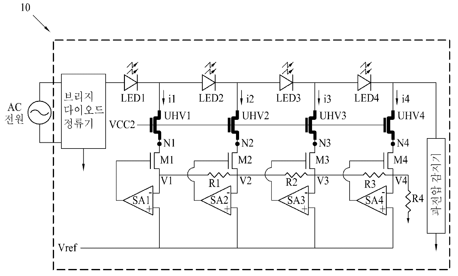
도 1을 참조하면, 본 발명의 일실시의 예에 따른 LED 구동부 회로(또는 간략히 구동부라 한다)(10)의 개략적인 다이어그램이 보여진다. 상술한 바와 같이, 상기 구동부(10)는 교류(AC) 전원과 같은 전원에 의하여 전원이 공급된다. 상기 AC 전원으로부터의 전류는 정류 회로에 의해 정류된다. 상기 정류 회로는 브리지 다이오드 정류기와 같이 상기 AC 전원으로부터의 교류 전력을 정류할 수 있는 적절한 정류회로일 수 있다. 상기 정류된 전압 Vrect은 LED의 스트링에 인가된다. 바람직하게는, 상기 AC 전원과 정류기는 직류(DC) 전원으로 대체될 수 있다.Referring to FIG. 1, a schematic diagram of an LED driver circuit (or simply a driver) 10 according to an embodiment of the present invention is shown. As described above, the
여기에서 사용되는 LED는 전통적인 LED, 초광도 LED, 고광도 LED, 유기LED 등과 같은 많은 다른 종류의 LED들에 있어서 일반적인 용어이다. 본 발명에서의 상기 구동부는 모든 종류의 LED에 적용할 수 있다.The LEDs used here are generic terms for many other types of LEDs, such as traditional LEDs, ultra-bright LEDs, high-intensity LEDs, organic LEDs, and the like. The driving unit of the present invention can be applied to all kinds of LEDs.
도 1에 도시된 바와 같이, LED의 스트링은 전기적으로 전원과 연결되고 4개의 그룹으로 나뉘어진다. 그러나, 상기 LED의 스트링은 어느 적당한 숫자의 그룹으로 나뉘어질 수 있음이 당업자에게 자명하다. 각 그룹의 LED들은 같거나 또는 다른 종류의, 이를 테면, 색상과 같은 조합으로 이루어질 수 있다. LED들은 직렬 또는 병렬로 연결되거나 또는 직렬과 병렬을 혼합하여 연결될 수 있다. 또한, 하나 이상의 저항들이 각 그룹에 포함될 수도 있다.As shown in FIG. 1, the LED strings are electrically connected to a power source and divided into four groups. However, it will be apparent to those skilled in the art that the string of LEDs may be divided into any suitable number of groups. The LEDs of each group may be of the same or a different kind, such as a combination of colors. The LEDs can be connected in series or in parallel, or they can be connected in series and parallel. Also, one or more resistors may be included in each group.
별도의 전류조절회로(또는 간략히 조절회로)는 집합적으로 전류의 흐름 i1을 조절하기 위한 구성 요소의 그룹으로서, LED 그룹 각각의 하향 끝단과 연결되고, 제1 트랜지스터(UHV1), 제2 트랜지스터(M1), 감지증폭기(SA1)를 포함한다. 이하에서는, 트랜지스터라는 용어는 N-채널 MOSFET, P-채널 MOSFET, NPN-양극성 트랜지스터, PNP-양극성 트랜지스터, 절연 게이트 양극성 트랜지스터(Insulated gate Bipolar Transistor), 아날로그 스위치 또는 계전기를 의미한다.A separate current regulating circuit (or simply regulating circuit) is collectively a group of components for regulating the current flow i1 and is connected to the downstream end of each of the LED groups and includes a first transistor UHV1, M1, and a sense amplifier SA1. In the following, the term transistor means an N-channel MOSFET, a P-channel MOSFET, an NPN-bipolar transistor, a PNP-bipolar transistor, an insulated gate bipolar transistor, an analog switch or a relay.
상기 제1 및 제2 트랜지스터는 전기적으로 직렬연결되어, 캐스코드(cascode) 구조를 이룬다. 상기 제1 트랜지스터는 높은 전압으로부터 상기 제2 트랜지스터를 보호할 수 있다. 이와 같이, 상기 제1 트랜지스터는 그 기능이 상기 제2 트랜지스터를 보호하는 것으로 한정하지 않을지라도 이하에서 보호 트랜지스터로 부른다. 상기 제2 트랜지스터의 주된 기능은 상기 전류i1을 조절하는 것을 포함하고, 그것으로써 상기 제2 트랜지스터는 이하에서 조절 트랜지스터로 부른다. 상기 보호 트랜지스터는, 예를 들면, 상기 조절 트랜지스터 M1이 저전압(LV)트랜지스터, 중전압(MV) 트랜지스터 또는 고전압(HV) 트랜지스터일 수 있으며 상기 보호 트랜지스터보다 낮은 파괴전압을 가지는 반면, 500V의 높은 파괴전압을 가지는 초고압 (UHV) 트랜지스터이다. N1 과 같은 노드는 상기 보호 트랜지스터의 소스가 상기 조절 트랜지스터의 드레인에 연결되는 지점이다.The first and second transistors are electrically connected in series to form a cascode structure. The first transistor may protect the second transistor from a high voltage. Thus, although the function of the first transistor is not limited to the protection of the second transistor, it is referred to as a protection transistor hereinafter. The main function of the second transistor includes adjusting the current i1, whereby the second transistor is hereinafter referred to as a regulating transistor. The protection transistor may, for example, be a low voltage (LV) transistor, a medium voltage (MV) transistor or a high voltage (HV) transistor and may have a lower breakdown voltage than the protection transistor, Voltage (UHV) transistor having a high voltage. A node such as N1 is the point where the source of the protection transistor is connected to the drain of the regulator transistor.
상기 감지증폭기(SA1)는 연산증폭기일수 있으며, 전압V1과 기준전압 Vref을 비교하고 상기 조절 트랜지스터의 게이트에 입력되는 신호를 출력하여, 상기 캐스코드와 저항 R1, R2, R3, R4를 흐르는 전류 i1 의 피드백제어를 형성한다. 상기 보호 트랜지스터의 게이트 전압은 상시전압 Vcc2로 설정될 수 있다 (이하에서는, Vcc2는 상시전압을 의미한다). 상기 상시 게이트 전압 Vcc2를 생성하는 메커니즘은 당분야에서 잘 알려져 있으며, 그것으로써 상기 메커니즘에 대한 자세한 설명은 본 명세서에서 기술하지 않는다.The sense amplifier SA1 may be an operational amplifier, compares the voltage V1 with the reference voltage Vref, and outputs a signal input to the gate of the regulating transistor to generate a current i1 flowing through the cascode resistor R1, R2, R3, Feedback control. The gate voltage of the protection transistor may be set to the constant voltage Vcc2 (hereinafter Vcc2 means constant voltage). The mechanism for generating the constant gate voltage Vcc2 is well known in the art, and therefore a detailed description of the mechanism is not described herein.
상기한 바와 같이, 각 전류조절회로는 전류 감지 저항기를 거쳐 일단의 해당 LED 그룹의 하향 끝단 및 타단의 그라운드와 전기적으로 연결되어 있다. 전압 V1, V2, V3, V4는 상기 조절 트랜지스터 M1, M2, M3, M4의 하향 끝단에서의 전위를 각각 나타낸다. 따라서, 예를 들면, 전압 V1은 다음의 식으로 나타낼 수 있다.As described above, each current control circuit is electrically connected to the ground at the lower end and the other end of the corresponding LED group at one end via the current sensing resistor. Voltages V1, V2, V3 and V4 represent potentials at the downstream ends of the regulating transistors M1, M2, M3 and M4, respectively. Therefore, for example, the voltage V1 can be expressed by the following equation.
V1 = i1*(R1 + R2 + R3 + R4) + i2*(R2 + R3 + R4) + i3*(R3 + R4) + i4*R4R4 = R4 + i2 * R2 + R3 + R4 + i3 * R3 + R4 +
구동부(10)는 정류된 전압Vrect의 준위가 변함에 따라 연속적으로 각 LED그룹을 온/오프할 수 있다. 전원의 전압이 0에서부터 증가하기 시작하면, 정류된 전압 Vrect는 전류가 LED를 흐르게 할 만큼 충분히 높지 않을 수 있다. 이 단계에서, 전압 V1, V2, V3, V4는 기준전압 Vref보다 낮고, 따라서, 감지증폭기 SA1, SA2, SA3, SA4 는 조절 트랜지스터 M1, M2, M3, M4를 각각 온(on)시킨다.The driving
전원의 전압이 전원의 하향 부분에 즉시 위치하는 제1 LED그룹인 LED1 (또는 그룹1)을 온(on) 시키기에 충분하게 증가되면, UHV1, M1, SA1를 포함하는 제1 전류조절회로는 도통되고 상기 전류 i1은 그라운드로 흐른다. 상기 제1 전류조절회로는 정류된 전압 Vrect가 LED1에 전원을 공급하기에 충분한 준위에 도달하기 전, 도달하는 때 또는 도달한 후에 온(on) 될 수 있다는 점을 유의해야 한다. 이와 같은 유추법은 그룹 2~4에 해당하는 다른 조절회로들에도 적용된다. 정류된 전압 Vrect가 LED1에 전원을 공급하기에 충분히 높지만 LED2를 온(on)시키기에 부족한 경우, 감지증폭기 SA1은 전압준위 V1과 기준전압 Vref를 비교하여, 제어 신호를 조절 트랜지스터 M1에 보낸다. 보다 자세하게, 감지증폭기 SA1의 출력 신호는 조절 트랜지스터 M1의 게이트에 입력된다.If the voltage of the power source is increased enough to turn on the LED 1 (or Group 1), which is the first group of LEDs immediately located in the downstream portion of the power source, the first current regulation circuit, including UHV1, M1, SA1, And the current i1 flows to the ground. It should be noted that the first current control circuit may be turned on after the rectified voltage Vrect reaches, or after reaching, a level sufficient to supply power to the
정류된 전압 Vrect이 증가함에 따라 LED1과 LED2에 전원을 공급하기에 충분한 준위에 도달한다. 그러면, 제2 조절회로(다시 말해서, UHV2, M2, SA2)는 도통되고, LED1과 LED2는 온(on)된다. 앞서 말한 바와 같이, 제2 전류조절회로는 정류된 전압 Vrect이 LED1과 LED2에 전원을 공급하기에 충분한 준위에 도달하기 전, 도달하는 때 또는 도달한 후에 온(on) 될 수 있다. 감지증폭기 SA2는 전압준위V2와 기준 전압 Vrect를 비교하여 제어 신호를 조절 트랜지스터 M2에 보낸다.As the rectified voltage Vrect increases, the level reaches a level sufficient to supply power to LED1 and LED2. Then, the second control circuit (i.e., UHV2, M2, SA2) is turned on, and LED1 and LED2 are turned on. As mentioned above, the second current regulating circuit can be turned on or after the rectified voltage Vrect reaches, reaches, or reaches a level sufficient to supply power to LED1 and LED2. The sense amplifier SA2 compares the voltage level V2 with the reference voltage Vrect and sends a control signal to the control transistor M2.
제2 전류조절회로가 온(on)인 경우, 전류 i1이 차단되면(또는 최소 준위로 설정되면) 구동부(10)의 전체 효율은 향상될 것이다. 이는 보다 많은 전류가 LED2를 흐르면 LED2가 더 많은 빛을 생산할 것이고, 전류i1의 차단(또는 감소)은 전류 i1이 LED2로 다시 향하게 하기 때문이다. 구동부(10)에 있어서, 전류i2가 흐르기 시작함에 따라, 전압V1은 보다 더 증가하고 어느 시점에서는 기준전압 Vref를 초과한다. 이 시점에서, 상기 SA1은 M1에 신호를 보내고 이로 인해 전류i1을 차단할 수 있다.When the second current control circuit is on, the total efficiency of the
연이은 그룹들에 대해서 같은 유추법이 적용된다. 일반적으로 말해서, 하향 LED 그룹이 온(on)이 되고 상기 하향 그룹과 연결된 전류조절회로가 도통되는 경우, 상향 그룹과 연결된 전류조절회로는 오프(off) (또는 조절회로를 흐르는 전류가 최소 준위로 설정)될 수 있어 구동부(10)의 전체적인 효율을 향상한다. The same analogy applies to subsequent groups. Generally speaking, when the downward LED group is turned on and the current regulating circuit connected to the downstream group is conducted, the current regulating circuit connected to the upstream group is turned off (or the current flowing in the regulating circuit is at the minimum level So that the overall efficiency of the driving
일단 소스 전압(또는 정류된 전압 Vrect)이 자신의 피크에 도달하고 하강하기 시작하면, 상기 과정은 반대로 진행되어 제1 전류조절회로가 마지막으로 다시 온(on)된다. 상기 소스 전압이 하향 그룹을 온(on)으로 유지하기에 충분하지 않은 준위로 감소하면, 하향 그룹과 연결된 조절회로가 온(on) 상태일지라도 하향 그룹은 자연스럽게 오프(off) 된다는 점을 유의해야 한다.Once the source voltage (or the rectified voltage Vrect) reaches its peak and begins to fall, the process is reversed and the first current regulation circuit is turned on last. It should be noted that if the source voltage is reduced to a level that is not sufficient to keep the downward group on, the downward group is naturally off even though the adjustment circuit associated with the downward group is on .
앞서 설명한 바와 같이, 각 조절회로는 직렬로 배열되어 캐스코드 구조를 형성하는 UHV1과 M1과 같은 두 개의 트랜지스터를 포함한다. 상기 캐스코드 구조는 전류 싱크(sink)로 구현되는데, 단일 트랜지스터 전류 싱크에 비해 다양한 장점을 가진다. 첫째, 전류구동능력을 향상시킨다. 전류 싱크에 대해 설계된 포화 영역에서 작동하는 경우, LV/MV/HV NMOS의 전류구동능력(Idrv)는 UHV NMOS보다 훨씬 우수하다. 예를 들면, 일반적인 UHV NMOS 의 전류구동능력(Idrv)이 10 ~ 20 ㎂/㎛인 반면, 일반적인 LV NMOS의 전류구동능력(Idrv)는 500 ㎂/㎛이다. 따라서, 동일한 양의 전류의 흐름을 조절하기 위하여, 칩상에서 UHV NMOS의 필요한 투사영역은 적어도 LV NMOS의 20배 이상이다. 또한, 일반적인 LV NMOS의 최소 채널 길이가 0.5 ㎛인 반면, 일반적인 UHV NMOS의 최소 채널 길이는 20 ㎛이다. 그러나, 일반적인 LV NMOS는 높은 전압으로부터의 보호를 제공하는 보호 메커니즘이 필요하다. 상기 캐스코드 구조에 있어서, 제2 트랜지스터, 바람직하게 LV/MV/HV NMOS는 전류조절기로 작용하는 반면, 제1 트랜지스터, 바람직하게 UHV NMOS는 보호 트랜지스터로 작용하여, 전류구동능력을 향상시킨다. 단일 UHV MNOS가 전류 싱크로 이용되고 선형 영역에서 작용되는 경우에서는 작용할 상기 보호 트랜지스터는 포화 영역에서는 작용하지 않는다. 이와 같이, 상기 전류구동능력 Idrv는 결정적 설계요소가 아니다. 오히려, 보호 트랜지스터의 저항Rdson이 캐스코드의 UHV NMOS를 설계하는 데 있어서 중요한 요소이다.As described above, each control circuit includes two transistors, such as UHV1 and M1, arranged in series to form a cascode structure. The cascode structure is implemented as a current sink, which has various advantages over a single transistor current sink. First, it improves current driving capability. The current drive capability (Idrv) of the LV / MV / HV NMOS is much better than the UHV NMOS when operating in the saturation region designed for the current sink. For example, the current driving capability Idrv of a general UHV NMOS is 10 to 20 占 / / 占 퐉 whereas the current driving capability Idrv of a typical LV NMOS is 500 占 퐉 / 占 퐉. Thus, in order to regulate the flow of the same amount of current, the required projection area of the UHV NMOS on the chip is at least 20 times the LV NMOS. In addition, the minimum channel length of a typical LV NMOS is 0.5 탆 whereas the minimum channel length of a general UHV NMOS is 20 탆. However, a typical LV NMOS requires a protection mechanism that provides protection from high voltages. In the cascode structure, the second transistor, preferably the LV / MV / HV NMOS, acts as a current regulator, while the first transistor, preferably the UHV NMOS, acts as a protection transistor to improve current drive capability. The protection transistor that will act in the case where a single UHV MNOS is used as a current sink and acts in a linear region does not work in the saturation region. Thus, the current driving capability Idrv is not a deterministic design element. Rather, the resistance Rdson of the protection transistor is an important factor in designing the UHV NMOS of the cascode.
둘째, 캐스코드 구조의 직렬 구성에 의하여, 캐스코드 구조의 필요한 전압(전압 준수 또는 전압 여유라고도 알려진)은 단일 UHV NMOS 구성보다 높을 수 있다. 그러나, LED 구동부의 경우, 필요한 전압으로 인한 전력손실은 LED 구동 전압으로 인한 전력손실보다 훨씬 적다. 예를 들면, AC로 구동되는 LED구동부에 있어서, LED 구동 전압(LED의 양(陽)극에 걸리는 전압)은 100 Vmrs에서 250 Vrms의 범위에 이른다. 캐스코드 구조의 필요한 전압은 5V인 반면, 단일 UHV NMOS의 필요한 전압은 2V이라고 가정하자. 이 경우, 효율은 각각 98 ~ 99 % 과 95 ~ 98 %이다. 물론, Rdson 은 감소될 수 있어서 캐스코드 구조의 필요한 전압은 단일 UHV NMOS의 필요한 전압과 거의 동일할 수 있다. 주안점은 캐스코드 구조가 소비하는 추가적인 전력은 사소한 단점이라는 것이다. 만약 효율이 중요한 설계요소라고 하면, 두 개의 UHV NMOS트랜지스터를 이용하는 전류미러(mirror)구성은 트랜지스터의 칩상에서의 넓은 영역으로 인하여 실제로는 가능하지 않은 반면, 캐스코드 구조는 전류미러구성으로 설계될 수 있다.Second, due to the cascode serial configuration, the required voltage (also known as voltage compliance or voltage margin) of the cascode structure can be higher than a single UHV NMOS configuration. However, in the case of the LED driver, the power loss due to the required voltage is much less than the power loss due to the LED driving voltage. For example, in an AC driven LED drive, the LED drive voltage (the voltage across the positive pole of the LED) ranges from 100 Vmrs to 250 Vrms. Assume that the required voltage of the cascode structure is 5V while the required voltage of a single UHV NMOS is 2V. In this case, the efficiencies are 98 to 99% and 95 to 98%, respectively. Of course, Rdson can be reduced so that the required voltage of the cascode structure can be approximately equal to the required voltage of a single UHV NMOS. The point is that the additional power consumed by the cascode structure is a minor drawback. If efficiency is an important design factor, the current mirror configuration using two UHV NMOS transistors is not actually possible due to the large area on the transistor's chip, whereas the cascode structure can be designed with a current mirror configuration have.
셋째, 상기 UHV NMOS 와 LV/MV/HV NMOS는 개별적으로 제어되기 때문에, 전류 싱크를 온/오프시키는 것은 상기 캐스코드 구조에서 보다 더 수월하다. 단일 UHV NMOS전류 싱크에 있어서, 전류조절 및 온/오프 작용은 대형 커패시터의 특징을 가지고 있는 UHV NMOS의 게이트를 제어함으로써 이루어져야 한다. 이와 대조적으로, 캐스코드 구조에 있어서는, 전류조절은 LV/MV/HV NMOS을 제어함으로써 이루어질 수 있고 온/오프작용은 게이트에 적용되는 논리연산만을 필요로 하는 UHV NMOS를 제어함으로써 이루어질 수 있다.Third, since the UHV NMOS and the LV / MV / HV NMOS are individually controlled, turning on / off the current sink is easier than in the cascade structure. In a single UHV NMOS current sink, the current regulation and on / off actions must be made by controlling the gate of the UHV NMOS, which has the characteristics of a large capacitor. In contrast, in a cascode configuration, the current regulation can be achieved by controlling the LV / MV / HV NMOS and the on / off operation can be achieved by controlling the UHV NMOS requiring only logic operations applied to the gate.
넷째, 온/오프시키는 속도는 단일 UHV NMOS 구성보다 캐스코드 구조에서 보다 원활하게 제어된다. 단일 UHV NMOS 구성에 있어서, 전류는 게이트 전압의 제곱함수이므로 전류의 선형제어는 게이트 전압을 제어함으로써 수월하게 이루어질 수 없다. 이에 비해, 캐스코드 구조에서는, LV/MV/HV NMOS의 게이트가 제어되는 경우, 전류는 게이트 전압의 역함수인 저항장치로서 작용하므로, 전류 제어(slewing)는 보다 원활해진다.Fourth, the on / off speed is controlled more smoothly in the cascode structure than in a single UHV NMOS configuration. In a single UHV NMOS configuration, the current is a function of the square of the gate voltage, so linear control of the current can not be made easily by controlling the gate voltage. In contrast, in the cascode structure, when the gate of the LV / MV / HV NMOS is controlled, the current acts as a resistance device which is an inverse function of the gate voltage, so that the slewing becomes smoother.
다섯째, 캐스코드 구조는 보다 나은 잡음여유도를 제공한다. 전원장치로부터의 잡음은 LED를 통하여 전파될 수 있으며, 이어서 전류조절회로와 결합할 수 있다. 보다 구체적으로, 잡음은 전류조절회로의 피드백루프로 유입된다. 단일 UHV NMOS 구성에 있어서, 이 잡음은 이 루프에 직접 결합된다. 반면에, 캐스코드 구조에 있어서는, 잡음은 LV/MV/HV NMOS의 유효한 저항에 대한 UHV NMOS의 Rdson의 비율에 따라 희석된다.Fifth, the cascode structure provides better noise margin. Noise from the power supply can be propagated through the LED and then coupled to the current regulating circuit. More specifically, noise enters the feedback loop of the current regulation circuit. In a single UHV NMOS configuration, this noise is directly coupled to this loop. On the other hand, in the cascode structure, the noise is diluted according to the ratio of Rdson of the UHV NMOS to the effective resistance of the LV / MV / HV NMOS.
여섯째, 캐스코드 구조에 의해서 생성된 잡음은 단일 UHV NMOS구성에서의 잡음보다 낮다. 캐스코드 구조에서는 전류제어가 주로 조절 트랜지스터에 의하여 이루어지는 반면, 단일 UHV NMOS구성에서는 전류제어가 UHV NMOS에 의하여 이루어진다. LV/MV/HV NMOS의 게이트 커패시턴스는 UHV NMOS의 게이트 커패시턴스보다 낮기 때문에, 캐스코드 구조에 의해서 생성된 잡음은 단일 UHV NMOS 구성에 의해서 생성된 잡음보다 낮다.Sixth, the noise generated by the cascode structure is lower than the noise in a single UHV NMOS configuration. In the cascode structure, the current control is mainly controlled by the regulating transistor, whereas in a single UHV NMOS configuration, the current control is performed by the UHV NMOS. Since the gate capacitance of the LV / MV / HV NMOS is lower than the gate capacitance of the UHV NMOS, the noise generated by the cascode structure is less than the noise generated by the single UHV NMOS configuration.
보호 트랜지스터 UHV1 ~ UHV4는 서로 동일하거나 상이할 수 있음을 유의해야 한다. 마찬가지로, 조절 트랜지스터 M1 ~ M4는 서로 동일하거나 상이할 수 있다. 보호 트랜지스터와 조절 트랜지스터에 대한 설명은 설계자의 목적을 충족시키도록 선택될 수 있다.It should be noted that the protection transistors UHV1 to UHV4 may be the same or different from each other. Likewise, the regulating transistors M1 to M4 may be the same or different from each other. The description of the protection transistor and the control transistor can be chosen to meet the designer's objectives.
도 2는 본 발명의 다른 실시의 예에 따른 LED 구동부 회로(20)의 개략적인 다이어그램을 나타낸다. 도시된 바와 같이, 구동부 회로(20)는 도 1에서의 구동부 회로(10)과 유사하고, 차이점은 감지기1, 감지기2, 감지기3이 노드 N2, N3, N4에서의 전압을 각각 감지하는데 사용되는 것이다. 예를 들면, 각 감지기는 연산증폭기, 인버터, (논리게이트) 또는 Schmitt 트리거가 될 수 있다. 각 감지기는 신호를 상향LED그룹과 연결된 감지증폭기로 신호를 보내서 전류조절회로를 흐르는 전류를 제어한다. 예를 들면, 정류된 전압 Vrect가 LED1과 LED2를 온(on)시키는 데 충분히 높다면, 감지기1은 노드 N2에서의 전압 준위를 모니터한다. 노드 N2에서의 전압이 더 증가하여 미리 설정한 전압 준위에 도달하면, 감지기1은 감지증폭기SA1으로 신호를 보낸다. 이어서, 감지증폭기 SA1은 조절 트랜지스터 M2의 게이트 전압을 조절하여 전류i1을 오프(off) 시킨다(또는 전류i1을 최소 준위로 설정한다). 일단 Vrect가 피크 준위에 도달하고 하강하면, 상기 과정이 반대로 진행된다.2 shows a schematic diagram of an
이와 같은 유추법은 다른 감지기에도 적용된다. 예를 들면, 감지기2는 노드N3에서의 전압 준위를 모니터하고 감지증폭기SA2로 신호를 보내서 전류의 흐름i2를 제어한다. 감지증폭기SA2 역시 기준전압Vref와 전압 V2를 비교하여 조절 트랜지스터 M2의 게이트 전압을 제어함을 유의해야 한다. 이리하여, 감지증폭기SA2는 3 개의 입력 전압(노드N3에서의 전압준위, 조절 트랜지스터M2의 하향 끝단에서의 전압V2, 기준 전압Vref)을 받아 전류흐름i2를 제어한다.This analogy also applies to other detectors. For example,
도 3은 본 발명의 또 다른 실시의 예에 따른 LED 구동부 회로(30)의 개략적인 다이어그램을 나타낸다. 도시된 바와 같이, 구동부 회로(30)는 구동부 회로(20)과 유사하며, 차이점은 감지기1~감지기3으로부터의 신호들이 상향 그룹의 감지증폭기의 기준 전압을 선택하는데 사용된다는 점이다. 예를 들면, 제1 기준 전압Vref1은 제2 기준 전압Vref2보다 낮다. 노드N3에서의 전압 준위가 미리 설정된 준위에 도달하는 경우, 감지기2는 스위치SW2에게 신호를 보내어 기준 전압은 Vref2에서 Vref1으로 스위칭된다. 그러면, 감지증폭기SA2의 출력 신호는 조절 트랜지스터 M2를 오프(off)시키도록 변경된다.3 shows a schematic diagram of an
도 4는 본 발명의 또 다른 실시의 예에 따른 LED 구동부 회로(40)의 개략적인 다이어그램을 나타낸다. 도시된 바와 같이, 구동부 회로(40)는 구동부 회로(10)과 유사하며, 차이점은 감지증폭기SA2의 출력 신호가 상향 감지증폭기SA1으로 입력된다는 점이다. 예를 들면, 전압V2가 미리 설정된 준위에 도달하는 경우, 감지증폭기SA2는 신호를 감지증폭기SA1으로 보내고, 이어서 감지증폭기SA1은 자신의 출력 전압준위를 감소시켜 조절 트랜지스터M1은 전류흐름i1을 오프(off)시킨다.Fig. 4 shows a schematic diagram of an
도 5는 본 발명의 또 다른 실시의 예에 따른 LED 구동부 회로(50)의 개략적인 다이어그램을 나타낸다. 도시된 바와 같이, 구동부 회로(50)는 구동부 회로(10)과 유사하며, 차이점은 감지증폭기SA1~SA3의 기준 전압은 Vref1과 Vref2사이에서 스위칭되고 상기 스위칭은 하향 감지증폭기의 출력 신호에 의해서 야기된다는 것이다. 예를 들면, 제1 기준 전압Vref1은 제2 기준 전압Vref2보다 낮다. 전압 V2가 미리 설정된 준위에 도달하는 경우, 감지증폭기SA2는 스위치SW1에 신호를 보내고 감지증폭기SA1의 비반전 전압이 Vref1으로 스위칭된다. 그러면, 비반전 입력으로서 Vref2(또는 Vref1)에 입력되는, 감지증폭기SA1의 출력 전압은 낮아져서 조절트랜지스터M1을 오프(off)시킨다.5 shows a schematic diagram of an
도 6은 본 발명의 또 다른 실시의 예에 따른 LED 구동부 회로(60)의 개략적인 다이어그램을 나타낸다. 도시된 바와 같이, 구동부 회로(60)는 도2의 구동부 회로(20)과 유사하며, 차이점은 각 감지기의 출력 핀(pin)이 상향 전류조절회로의 제1 트랜지스터의 게이트와 연결된다는 것이다. 각 감지기는 상향 LED그룹과 연결되어 있는 제1(또는 보호) 트랜지스터의 게이트에 출력 신호를 보내어 전류조절회로를 흐르는 전류를 제어한다. 예를 들면, 정류된 전압Vrect가 LED1과 LED2를 온(on) 시키기에 충분히 높은 경우, 감지기1은 노드N2에서의 전압 준위를 모니터한다. 노드N2에서의 전압이 더 증가하여 미리 설정된 전압 준위에 도달함에 따라, 감지기1은 UHV1의 게이트로 출력 신호를 보낸다. 이어서, UHV1은 전류i1을 오프(off)시킨다(또는 전류i1을 최소 준위로 설정한다).6 shows a schematic diagram of an
이와 같은 유추법은 다른 감지기에도 적용된다. 예를 들면, 감지기2는 노드N3에서의 전압 준위를 모니터하고 UHV2에 출력 신호를 전송하여 전류의 흐름i2를 제어한다. 마지막LED그룹인 LED4와 연결된 전류조절회로의 제1 트랜지스터인 UHV4는 상시 게이트전압Vcc2를 가짐을 유의해야 한다.This analogy also applies to other detectors. For example,
도 7은 본 발명의 또 다른 실시의 예에 따른 LED 구동부 회로(70)의 개략적인 다이어그램을 나타낸다. 도시된 바와 같이, 구동부 회로(70)은 도1의 구동부 회로(10)와 유사하며, 차이점은 감지증폭기의 출력 핀이 상향 전류조절회로의 제1 트랜지스터의 게이트에 연결되어 상향 전류조절회로를 흐르는 전류를 제어한다는 것이다. 예를 들면, 정류된 전압Vrect 가 LED1과 LED2를 온(on) 시키기에 충분히 높은 경우, 감지증폭기SA2는 UHV1의 게이트에 출력 신호를 전송한다. 이어서, UHV1은 전류i1을 오프(off) 시킨다(또는 전류i1을 최소 준위로 설정한다).7 shows a schematic diagram of an
이와 같은 유추법은 다른 감지기에도 적용된다. 예를 들면, 감지기3은 UHV2에 출력 신호를 전송하여 전류의 흐름i2를 제어한다. 마지막LED그룹인 LED 4에 연결된 전류조절회로의 제1 트랜지스터인 UHV4는 상시 게이트전압Vcc2를 가짐을 유의해야 한다.This analogy also applies to other detectors. For example, detector 3 sends an output signal to UHV2 to control current flow i2. It should be noted that UHV4, which is the first transistor of the current regulation circuit connected to LED 4, which is the last LED group, always has gate voltage Vcc2.
도 8a는 조절 트랜지스터M을 흐르는 전류i를 제어하기 위한 회로(80)의 개략적인 다이어그램을 보여준다. 회로(80)은 상기 구동부 회로들(10 ~ 70)에 포함된다. 도시된 바와 같이, 감지증폭기SA는 기준 전압Vref와 노드N에서의 전압 준위를 비교하여 조절 트랜지스터M의 게이트로 신호를 전송하여 전류i를 제어한다. 상기 회로(80)의 구성 요소들의 유형과 작동 메커니즘은 도1과 연계하여 상술한다. 예를 들면, 보호 트랜지스터가 UHV NMOS 인 반면, 조절 트랜지스터 M은 LV/MV/HV NMOS일 수 있다. 간결한 설명을 위해서 다른 구성 요소들의 설명은 반복하지 않는다.8A shows a schematic diagram of a
도 8b는 본 발명의 또 다른 실시의 예에 따라 조절 트랜지스터M1을 흐르는 전류i를 제어하기 위한 회로(82)의 개략적인 다이어그램을 보여준다. 도시된 바와 같이, 또 다른 트랜지스터 M2는 조절 트랜지스터M1과 동일하고 조절 트랜지스터M1에 연결되어 전류미러구성을 형성한다. 보다 자세하게는, 두 트랜지스터M1과 M2의 게이트는 전기적으로 서로 연결되어 같은 게이트 전압을 갖는다. 제2 트랜지스터M2를 흐르는 전류Iref는 조절 트랜지스터M1을 흐르는 전류i를 조절하도록 제어된다. 상기 전류조절회로(82)는 도 8a의 전류조절회로(80)을 대신하여 사용될 수 있고, 이와 같이 전류조절회로(82)는 도 1 ~ 7의 구동부 회로들에 사용될 수 있다. 더욱이, 전류Iref는 하나의 준위에서 다른 준위로 변환하여 구동부 회로들(30과 50)에서의 Vref1에서 Vref2까지 기준 전압을 스위칭하는 효과를 가질 수 있다.Figure 8b shows a schematic diagram of a
도 8c는 본 발명의 또 다른 실시의 예에 따라 조절 트랜지스터M을 흐르는 전류i를 제어하기 위한 회로(84)의 개략적인 다이어그램을 보여준다. 도시된 바와 같이, 다음의 식으로 정해지는 비반전 입력 전압Vref가 감지증폭기SA에 공급된다.8C shows a schematic diagram of a
Vref = Iref*RVref = Iref * R
여기서, Iref와 R은 전류와 저항을 각각 나타낸다.Here, Iref and R represent a current and a resistance, respectively.
전류조절회로(84)는 도 8a의 전류조절회로(80)을 대신하여 사용될 수 있다. 이와 같이, 전류조절회로(84)는 도1~7의 구동부 회로들에 사용될 수 있다. 더욱이, 전류Iref는 하나의 준위에서 다른 준위로 변환하여 구동부 회로들(30과 50)에서의 Vref1에서 Vref2까지 기준 전압을 스위칭하는 효과를 가질 수 있다.The
두 개의 기준 전압Vref1과 Vref2만이 구동부 회로들(30과 50)의 각 스위치에 대해 사용되는 것을 유의해야 한다. 그러나, 두 개 이상의 기준 전압이 각 스위치에 대해 사용될 수 있음이 당업자에게는 자명하다.It should be noted that only two reference voltages Vref1 and Vref2 are used for each switch of the
도 9는 본 발명의 또 다른 실시의 예에 따른 과전압 감지기(92)의 개략적인 다이어그램을 나타낸다. 도시된 바와 같이, 과전압 감지기(92)는 마지막LED그룹의 하향 끝단에 연결되는 제너(Zener) 다이오드; 전압을 감지하는 감지기(94); 및 감지저항R을 포함할 수 있다. 노드Z1에서의 전압 준위는 LED스트링에 의하여 Vrect와 전압 강하의 전압 차이와 같다. Z1에서의 전압 준위가 미리 설정된 준위, 바람직하게는 제너 다이오드의 파괴전압을 초과하는 경우, 전류는 감지저항R을 흐른다. 그러면, 감지기(94)는 전압 준위를 감지하고 구동부 회로의 적절한 구성 요소에 신호를 전송하여 LED를 흐르는 전류를 제어 즉, LED를 흐르는 전류를 차단하거나 구동부 회로를 포함하는 칩에서의 과도한 전력소모를 방지한다. 예를 들면, 과전압 감지기(92)의 출력 신호가 도1의 SA4에 입력되어 전류i4 가 차단된다. 다른 예로는, 상기 출력 신호가 기준 전압Vref를 생성하는 구성 요소(도 1에는 도시되지 않음)로 전송되어 상기 구성 요소는 도 1에서의 Vref를 감소시킬 수 있다. 또 다른 예로는, 상기 출력 신호가 보호 트랜지스터들 UHVs의 게이트 전압Vcc2를 낮추는 데 이용된다. 상기 과전압 감지기(92)는 또한 도 1 ~ 7의 구동부 회로들에도 사용 될 수 있음을 유의해야 한다.9 shows a schematic diagram of an over-voltage sensor 92 in accordance with another embodiment of the present invention. As shown, the overvoltage sensor 92 comprises a Zener diode connected to the lower end of the last group of LEDs; A sensor 94 for sensing a voltage; And a sense resistor R. < RTI ID = 0.0 > The voltage level at node Z1 is equal to the voltage difference between Vrect and voltage drop due to the LED string. If the voltage level at Z1 exceeds a predetermined level, preferably the breakdown voltage of the Zener diode, the current flows through the sense resistor R. [ The detector 94 then senses the voltage level and sends a signal to the appropriate components of the driver circuit to control the current flowing through the LED, i. E., To cut off the current flowing through the LED, or < / RTI > prevent. For example, the output signal of the overvoltage detector 92 is input to SA4 in Fig. 1, and the current i4 is interrupted. As another example, the output signal may be sent to a component (not shown in FIG. 1) that produces a reference voltage Vref so that the component can reduce Vref in FIG. As another example, the output signal is used to lower the gate voltage Vcc2 of the protection transistors UHVs. It should be noted that the overvoltage sensor 92 may also be used in the driver circuitry of Figs. 1-7.
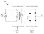
도 1~7에 도시된 바와 같이, 각 구동부는 AC 전원으로부터 공급되는 전류를 정류하는 정류기를 포함할 수 있다. 고전력 LED 가로등과 같은 특정 응용분야에 있어서, LED 는 높은 전력 소비를 요구할 수 있다. 이러한 분야에서 구동부는 안전을 목적으로 변압기에 의해 교류 전원과 격리될 수 있다. As shown in Figs. 1 to 7, each driving unit may include a rectifier for rectifying a current supplied from an AC power source. For certain applications, such as high power LED street lamps, LEDs may require high power consumption. In this field, the drive can be isolated from the AC power source by a transformer for safety purposes.
도 10a 내지 도 10b는 본 발명의 또 다른 실시의 예에 따른 입력전원 생성기(100 및 110)의 개략적인 다이어그램을 나타낸다. 도 10a에 도시된 바와 같이, 변압기(104)는 AC입력소스와 정류기(102) 사이에 배치될 수 있다. 아니면, 도 10b에 도시된 바와 같이, 정류기(112)는 AC입력소스와 변압기(114) 사이에 배치될 수 있다. 두 경우에 있어서, 전류i는 동작 중에 하나 또는 그 이상의 LED그룹을 흐른다. 입력 전원 생성기(100 및 110)는 도 1 ~ 7의 구동부에 적용될 수 있다.10A-10B illustrate schematic diagrams of
물론, 상기 설명한 사항은 본 발명의 모범적인 실시의 예와 관련되어 있으며 그 변경은 다음의 청구범위에 명시된 바와 같이 본 발명의 기술적 사상과 범위에서 벗어나지 않고 실시될 수 있음이 이해되어야 할 것이다.It is to be understood, however, that the foregoing is directed to exemplary embodiments of the invention and that modifications may be made without departing from the spirit and scope of the invention as set forth in the following claims.
Claims (32)
상기 LED 스트링에 전기적으로 연결되는 전원을 제공하는 단계;
제1트랜지스터 및 제2트랜지스터를 가지는 캐스코드(cascode) 구조를 포함하는 별도의 전류조절회로를 통하여 상기 각 그룹을 그라운드에 결합시키는 단계;
상향 그룹의 전류조절회로의 하향 끝단을 다음 하향 그룹의 전류조절회로의 하향 끝단과 저항을 사이에 두고 연결시키는 단계; 및
상기 전원으로부터의 입력전압을 증가시켜 하향 순서로 상기 그룹들을 온(on)시키는 단계를 포함하는,
발광다이오드(LED)를 구동하는 방법.Providing an LED string that is divided into electrically connected groups in series;
Providing a power source electrically coupled to the LED string;
Coupling each group to ground through a separate current control circuit including a cascode structure having a first transistor and a second transistor;
Connecting the downstream end of the current control circuit of the upstream group to the downstream end of the current control circuit of the next downstream group with a resistor interposed therebetween; And
Increasing the input voltage from the power supply to turn on the groups in a downward order,
A method of driving a light emitting diode (LED).
상기 제1 트랜지스터의 게이트에 게이트 전압을 인가하는 단계; 및
상기 제2 트랜지스터의 게이트 전압을 변경하여 상기 제2 트랜지스터를 흐르는 전류를 조절하는 단계를 더 포함하며,
상향 그룹의 다음 하향 그룹의 전류가 미리 설정한 준위에 도달할 때, 상기 상향 그룹의 상기 제2 트랜지스터를 흐르는 전류는 최소 준위로 감소되거나 오프(off)되는,
발광다이오드(LED)를 구동하는 방법.The method according to claim 1,
Applying a gate voltage to a gate of the first transistor; And
And adjusting a current flowing through the second transistor by changing a gate voltage of the second transistor,
The current flowing through the second transistor in the upper group is reduced or turned off to a minimum level when the current of the next lower group of the upper group reaches a preset level,
A method of driving a light emitting diode (LED).
상기 제1 트랜지스터의 게이트에 게이트 전압을 인가하는 단계는 상시 준위에서 상기 제1 트랜지스터의 게이트에 인가된 게이트 전압을 유지하는 단계를 포함하는,
발광다이오드(LED)를 구동하는 방법.3. The method of claim 2,
Wherein applying the gate voltage to the gate of the first transistor comprises maintaining the gate voltage applied to the gate of the first transistor at a constant level,
A method of driving a light emitting diode (LED).
상기 별도의 전류조절회로는 감지증폭기를 포함하고, 상기 제2 트랜지스터를 흐르는 전류를 조절하는 단계는
기준 전압을 상기 감지증폭기로 입력하는 단계; 및
상기 감지증폭기로 하여금 출력 신호를 상기 제2 트랜지스터의 게이트로 전송하도록 하여 상기 제2 트랜지스터를 흐르는 전류를 조절하는 단계를 포함하는,
발광다이오드(LED)를 구동하는 방법.3. The method of claim 2,
Wherein the separate current control circuit includes a sense amplifier, and the step of adjusting the current flowing through the second transistor comprises:
Inputting a reference voltage to the sense amplifier; And
And controlling the current flowing through the second transistor by causing the sense amplifier to transmit an output signal to the gate of the second transistor.
A method of driving a light emitting diode (LED).
상기 감지증폭기로 하여금 출력 신호를 전송하도록 하는 단계에 앞서,
감지기로 하여금 하향 그룹의 제2 트랜지스터의 드레인 전압을 모니터하게 하는 단계; 및
상기 감지기로 하여금 출력 신호를 상기 하향 그룹의 다음 상향 그룹의 감지증폭기로 전송하도록 하는 단계를 더 포함하는,
발광다이오드(LED)를 구동하는 방법.5. The method of claim 4,
Prior to the step of causing the sense amplifier to transmit an output signal,
Causing a detector to monitor a drain voltage of a second transistor in a downward group; And
Further comprising causing the detector to transmit an output signal to a sense amplifier of a next up group of the downward group,
A method of driving a light emitting diode (LED).
상기 기준 전압을 입력하는 단계에 앞서,
제1 및 제2 상시 전압을 제공하는 단계;
감지기로 하여금 하향 그룹의 제2 트랜지스터의 드레인 전압을 모니터하게 하는 단계;
상기 드레인 전압이 미리 설정된 준위에 도달할 때, 상기 감지기로 하여금 출력 신호를 전송하도록 하는 단계; 및
상기 감지기의 출력 신호를 근거로, 제1 및 제2 실질적 상시 전압 중 하나를 하향 그룹의 다음 상향 그룹의 감지 트랜지스터의 기준 전압으로 선택하는 단계를 더 포함하는,
발광다이오드(LED)를 구동하는 방법.5. The method of claim 4,
Prior to the step of inputting the reference voltage,
Providing a first and a second constant voltage;
Causing a detector to monitor a drain voltage of a second transistor in a downward group;
Causing the detector to transmit an output signal when the drain voltage reaches a predetermined level; And
Further comprising selecting one of the first and second substantially constant voltages as the reference voltage of a sense transistor of a next up group of the downward group, based on the output signal of the detector,
A method of driving a light emitting diode (LED).
상기 감지증폭기로 하여금 출력 신호를 전송하도록 하는 단계 이후에,
하향 그룹의 감지증폭기로 하여금 상기 출력 신호를 상기 하향 그룹의 다음 상향 그룹의 감지증폭기로 전송하도록 하는 단계를 더 포함하는,
발광다이오드(LED)를 구동하는 방법.5. The method of claim 4,
After the step of causing the sense amplifier to transmit an output signal,
Further comprising causing the sense amplifiers in the downward group to transmit the output signals to the sense amplifiers in the next up group of the downward group.
A method of driving a light emitting diode (LED).
상기 기준 전압을 입력하는 단계에 앞서,
제1 및 제2 상시 전압을 제공하는 단계;
하향 그룹의 감지증폭기로 하여금 출력 신호를 전송하도록 하는 단계; 및
상기 하향 그룹의 감지증폭기의 출력 신호를 근거로, 상기 제1 및 제2 실질적 상시 전압 중 하나를 상기 하향 그룹의 다음 상향 그룹의 감지 트랜지스터의 기준 전압으로 선택하는 단계를 더 포함하는,
발광다이오드(LED)를 구동하는 방법.5. The method of claim 4,
Prior to the step of inputting the reference voltage,
Providing a first and a second constant voltage;
Causing the sense amplifier of the downstream group to transmit an output signal; And
Further comprising selecting one of said first and second substantially constant voltages as a reference voltage of a sense transistor of a next up group of said downward group, based on an output signal of said sense amplifier of said downward group,
A method of driving a light emitting diode (LED).
기준 전압을 입력하는 단계에 앞서,
기준 전류로 하여금 저항을 흐르도록 하는 단계; 및
상기 저항에 걸친 전압 차이를 상기 기준 전압으로 취하는 단계를 더 포함하는,
발광다이오드(LED)를 구동하는 방법.5. The method of claim 4,
Prior to the step of inputting the reference voltage,
Causing the reference current to flow through the resistor; And
Further comprising the step of taking a voltage difference across the resistor as the reference voltage.
A method of driving a light emitting diode (LED).
게이트 전압을 상기 제1 트랜지스터의 게이트에 인가하는 단계는
감지기로 하여금 하향 그룹의 제2 트랜지스터의 드레인 전압을 모니터하도록 하는 단계; 및
상기 감지기로 하여금 상기 하향 그룹의 다음 상향 그룹의 제1 트랜지스터의 게이트에 출력 신호를 전송하도록 하는 단계를 포함하는,
발광다이오드(LED)를 구동하는 방법.3. The method of claim 2,
The step of applying a gate voltage to the gate of the first transistor
Causing a detector to monitor a drain voltage of a second transistor in a downward group; And
And causing the detector to transmit an output signal to a gate of a first transistor of a next up group of the downward group.
A method of driving a light emitting diode (LED).
상기 별도의 전류조절회로는 감지증폭기를 포함하며, 게이트 전압을 상기 제1 트랜지스터의 게이트에 인가하는 단계는 하향 그룹의 감지증폭기로 하여금 상기 하향 그룹의 다음 상향 그룹의 제1 트랜지스터의 게이트에 출력 신호를 전송하도록 하는 단계를 포함하는,
발광다이오드(LED)를 구동하는 방법.3. The method of claim 2,
Wherein the step of applying the gate voltage to the gate of the first transistor causes the sense amplifiers of the downstream group to output the output signal to the gate of the first transistor of the next upstream group of the downstream group, The method comprising:
A method of driving a light emitting diode (LED).
상기 별도의 전류조절회로는 상기 제2 트랜지스터와 동일한 제3 트랜지스터를 포함하고, 상기 제2 트랜지스터의 게이트는 상기 제3 트랜지스터의 게이트와 직접 연결되어 전류미러를 형성하며, 상기 제2 트랜지스터를 흐르는 전류를 상기 제3 트랜지스터를 흐르는 전류로 변경함으로써 조절하는 단계를 더 포함하는,
발광다이오드(LED)를 구동하는 방법.The method according to claim 1,
Wherein the current control circuit includes a third transistor that is the same as the second transistor, the gate of the second transistor is directly connected to the gate of the third transistor to form a current mirror, and the current flowing through the second transistor To the current flowing through the third transistor. ≪ RTI ID = 0.0 >
A method of driving a light emitting diode (LED).
제너(Zener) 다이오드와 저항을 LED스트링의 하향 끝단과 그라운드 사이에 직렬로 배치하는 단계;
감지기로 하여금 저항의 지점에서의 전압 준위를 모니터하도록 하는 단계;
전류가 상기 제너 다이오드를 흐르는 경우, 상기 감지기로 하여금 출력 신호를 전송하도록 하는 단계; 및
상기 감지기의 출력 신호를 근거로, LED스트링을 흐르는 전류를 제어하는 단계를 더 포함하는,
발광다이오드(LED)를 구동하는 방법.The method according to claim 1,
Disposing a Zener diode and a resistor in series between the lower end of the LED string and the ground;
Causing the detector to monitor a voltage level at a point of resistance;
Causing the detector to transmit an output signal when a current flows through the Zener diode; And
Further comprising controlling the current flowing through the LED string based on an output signal of the detector,
A method of driving a light emitting diode (LED).
상기 전류를 제어하는 단계는
감지증폭기로 하여금 상기 감지기의 출력 신호를 수신받도록 하는 단계; 및
상기 감지증폭기로 하여금 상기 제2 트랜지스터의 게이트로 신호를 전송하도록 하는 단계를 포함하는,
발광다이오드(LED)를 구동하는 방법.14. The method of claim 13,
The step of controlling the current
Causing the sense amplifier to receive an output signal of the detector; And
And causing the sense amplifier to transmit a signal to a gate of the second transistor.
A method of driving a light emitting diode (LED).
상기 전류를 제어하는 단계는
상기 감지기의 출력 신호를 근거로 기준 전압을 변경하는 단계; 및
상기 변경된 기준 전압을 감지증폭기로 입력하는 단계를 포함하고,
상기 감지증폭기의 출력 신호는 상기 제2 트랜지스터의 게이트로 직접 입력되는,
발광다이오드(LED)를 구동하는 방법.14. The method of claim 13,
The step of controlling the current
Changing a reference voltage based on an output signal of the detector; And
And inputting the changed reference voltage to a sense amplifier,
The output signal of the sense amplifier being directly input to the gate of the second transistor,
A method of driving a light emitting diode (LED).
상기 전류를 제어하는 단계는
상기 감지기의 출력 신호를 이용하여 상기 제1 트랜지스터의 게이트 전압을 변경하는 단계를 포함하는,
발광다이오드(LED)를 구동하는 방법.14. The method of claim 13,
The step of controlling the current
And changing the gate voltage of the first transistor using the output signal of the detector.
A method of driving a light emitting diode (LED).
그룹1의 상향 끝단과 결합하여 입력 전압을 제공하는 전원; 및
일단의 해당 그룹의 하향 끝단 및 타단의 그라운드와 결합하고, 감지증폭기 및 제1 트랜지스터와 제2 트랜지스터를 가지는 캐스코드를 포함하는 복수의 전류조절회로를 포함하고,
상향 그룹의 전류조절회로의 하향 끝단은 다음 하향 그룹의 전류조절회로의 하향 끝단과 저항을 사이에 두고 연결되어 있는,
발광다이오드(LED)를 구동하는 구동부 회로.an LED string divided into n groups, LEDs of the n groups electrically connected in series with each other, a downward end of the group m-1 electrically connected to the upper end of the group m, m being an amount less than or equal to n Number;
A power supply coupled to the upper end of group 1 to provide an input voltage; And
And a plurality of current control circuits coupled to the ground at the other end of the group of the group and including a sense amplifier and a cascode having a first transistor and a second transistor,
The downstream end of the current control circuit of the upstream group is connected to the downstream end of the current control circuit of the next downstream group,
A driver circuit for driving a light emitting diode (LED).
상기 제1 트랜지스터는 초고압 (UHV) 트랜지스터, N-채널 MOSFET, P-채널 MOSFET, NPN-양극성 트랜지스터, PNP-양극성 트랜지스터 및 절연 게이트 양극성 트랜지스터(IGBT) 중 하나인, 발광다이오드(LED)를 구동하는 구동부 회로.18. The method of claim 17,
The first transistor drives a light emitting diode (LED), which is one of an ultra high voltage (UHV) transistor, an N-channel MOSFET, a P-channel MOSFET, an NPN-bipolar transistor, a PNP-bipolar transistor and an insulated gate bipolar transistor Drive circuit.
상기 제2 트랜지스터는 저전압(LV)트랜지스터, 중전압(MV) 트랜지스터 및 고전압(HV) 트랜지스터, N-채널 MOSFET, P-채널 MOSFET, NPN-양극성 트랜지스터, PNP-양극성 트랜지스터 및 절연 게이트 양극성 트랜지스터(IGBT) 중 하나인, 발광다이오드(LED)를 구동하는 구동부 회로.18. The method of claim 17,
The second transistor includes a low voltage (LV) transistor, a medium voltage (MV) transistor and a high voltage (HV) transistor, an N-channel MOSFET, a P-channel MOSFET, an NPN-bipolar transistor, a PNP- ) Driving the light emitting diode (LED).
각각이 그룹 m에 해당하는 상기 전류조절회로의 제1 트랜지스터의 소스 전압을 감지하고 그룹 m-1에 해당하는 상기 전류조절회로의 감지증폭기로 신호를 전송하도록 적용되는 복수의 감지기를 더 포함하는,
발광다이오드(LED)를 구동하는 구동부 회로.18. The method of claim 17,
Further comprising a plurality of detectors each adapted to sense a source voltage of a first transistor of the current regulation circuit corresponding to group m and to transmit a signal to a sense amplifier of the current regulation circuit corresponding to group m-1,
A driver circuit for driving a light emitting diode (LED).
각각이 두 개의 기준 전압 사이에서 스위치하도록 적용되고 해당 전류조절회로의 감지증폭기에 연결되는 복수의 스위치; 및
각각이 그룹 m에 해당하는 상기 전류조절회로의 제1 트랜지스터의 소스 전압을 감지하고 그룹 m-1에 해당하는 스위치로 신호를 전송하도록 적용되는 복수의 감지기를 더 포함하는,
발광다이오드(LED)를 구동하는 구동부 회로.18. The method of claim 17,
A plurality of switches each adapted to switch between two reference voltages and to a sense amplifier of the current regulating circuit; And
Further comprising: a plurality of detectors each adapted to sense a source voltage of a first transistor of the current regulation circuit corresponding to group m and to transmit a signal to a switch corresponding to group m-1,
A driver circuit for driving a light emitting diode (LED).
그룹m에 해당하는 상기 전류조절회로의 감지증폭기의 출력 핀은 그룹m-1의 감지증폭기에 직접 연결되는,
발광다이오드(LED)를 구동하는 구동부 회로.18. The method of claim 17,
The output pin of the sense amplifier of the current control circuit corresponding to the group m is directly connected to the sense amplifier of the group m-1,
A driver circuit for driving a light emitting diode (LED).
그룹m에 해당하는 상기 전류조절회로의 감지증폭기의 출력 핀은 그룹m-1의 감지증폭기에 직접 연결되고,
각각이 두 개의 기준 전압 사이에서 스위치하도록 적용되고 해당 전류조절회로의 감지증폭기에 연결되는 복수의 스위치를 더 포함하고,
그룹m에 해당하는 상기 전류조절회로의 감지증폭기의 출력 핀은 그룹m-1에 해당하는 스위치에 연결되는,
발광다이오드(LED)를 구동하는 구동부 회로.18. The method of claim 17,
The output pin of the sense amplifier of the current control circuit corresponding to the group m is directly connected to the sense amplifier of the group m-1,
Further comprising a plurality of switches each adapted to switch between two reference voltages and to a sense amplifier of the current regulating circuit,
The output pin of the sense amplifier of the current control circuit corresponding to the group m is connected to the switch corresponding to the group m-1,
A driver circuit for driving a light emitting diode (LED).
각각이 그룹 m에 해당하는 상기 전류조절회로의 제1 트랜지스터의 소스 전압을 감지하고 그룹 m-1에 해당하는 상기 전류조절회로의 제1 트랜지스터의 게이트로 신호를 전송하도록 적용되는 복수의 감지기를 더 포함하는,
발광다이오드(LED)를 구동하는 구동부 회로.18. The method of claim 17,
A plurality of detectors each adapted to sense the source voltage of the first transistor of the current regulation circuit corresponding to group m and to transmit a signal to the gate of the first transistor of the current regulation circuit corresponding to group m-1 Including,
A driver circuit for driving a light emitting diode (LED).
그룹m에 해당하는 상기 전류조절회로의 감지증폭기의 출력 핀은 그룹m-1에 해당하는 상기 전류조절회로의 제1 트랜지스터의 게이트에 직접 연결되는,
발광다이오드(LED)를 구동하는 구동부 회로.18. The method of claim 17,
The output pin of the sense amplifier of the current control circuit corresponding to the group m is directly connected to the gate of the first transistor of the current control circuit corresponding to the group m-1,
A driver circuit for driving a light emitting diode (LED).
상기 각 전류조절회로는 상기 제2 트랜지스터와 동일한 제3 트랜지스터를 포함하고, 상기 제3 트랜지스터의 게이트는 상기 제2 트랜지스터의 게이트와 직접 연결되어 전류미러를 형성하는,
발광다이오드(LED)를 구동하는 구동부 회로.18. The method of claim 17,
Wherein each current control circuit includes a third transistor that is the same as the second transistor and the gate of the third transistor is directly connected to the gate of the second transistor to form a current mirror,
A driver circuit for driving a light emitting diode (LED).
상기 각 전류조절회로의 감지증폭기는 기준 전압 제공을 위한 전압 소스에 연결되고, 상기 전압 소스는 기준 전류 소스와 저항을 포함하는,
발광다이오드(LED)를 구동하는 구동부 회로.18. The method of claim 17,
Wherein the sense amplifier of each current regulation circuit is connected to a voltage source for providing a reference voltage, the voltage source comprising a reference current source and a resistor,
A driver circuit for driving a light emitting diode (LED).
LED스트링의 하향 끝단에 연결되는 과전압 감지기를 더 포함하는,
발광다이오드(LED)를 구동하는 구동부 회로.18. The method of claim 17,
Further comprising an overvoltage detector coupled to a downstream end of the LED string,
A driver circuit for driving a light emitting diode (LED).
상기 과전압 감지기는 제너(Zener) 다이오드, 저항 및 상기 저항의 지점에서의 전압을 감지하도록 적용되는 감지기를 포함하는,
발광다이오드(LED)를 구동하는 구동부 회로.30. The method of claim 29,
Wherein the overvoltage sensor comprises a Zener diode, a resistor and a detector adapted to sense a voltage at a point of the resistor,
A driver circuit for driving a light emitting diode (LED).
각각이 그라운드와 해당 그룹의 제2 트랜지스터의 소스 사이에 배치되는 복수의 저항을 더 포함하는,
발광다이오드(LED)를 구동하는 구동부 회로.18. The method of claim 17,
Further comprising a plurality of resistors each disposed between a ground and a source of a second transistor of the group,
A driver circuit for driving a light emitting diode (LED).
상기 전원은 정류기와 변압기를 포함하는,
발광다이오드(LED)를 구동하는 구동부 회로.
18. The method of claim 17,
Wherein the power source comprises a rectifier and a transformer,
A driver circuit for driving a light emitting diode (LED).
Applications Claiming Priority (5)
| Application Number | Priority Date | Filing Date | Title |
|---|---|---|---|
| US42212810P | 2010-12-11 | 2010-12-11 | |
| US61/422,128 | 2010-12-11 | ||
| US13/244,873 US9144123B2 (en) | 2010-12-11 | 2011-09-26 | Light emitting diode driver having cascode structure |
| US13/244,873 | 2011-09-26 | ||
| PCT/US2011/001926 WO2012078181A2 (en) | 2010-12-11 | 2011-11-21 | Light emitting diode driver having cascode structure |
Publications (2)
| Publication Number | Publication Date |
|---|---|
| KR20130117825A KR20130117825A (en) | 2013-10-28 |
| KR101658052B1 true KR101658052B1 (en) | 2016-09-22 |
Family
ID=46198654
Family Applications (3)
| Application Number | Title | Priority Date | Filing Date |
|---|---|---|---|
| KR1020137016993A Expired - Fee Related KR101658054B1 (en) | 2010-12-11 | 2011-11-21 | Light emitting diode driver |
| KR1020137016991A Active KR101658052B1 (en) | 2010-12-11 | 2011-11-21 | Light emitting diode driver having cascode structure |
| KR1020137016996A Expired - Fee Related KR101658059B1 (en) | 2010-12-11 | 2011-11-21 | Light emitting diode driver having phase control mechanism |
Family Applications Before (1)
| Application Number | Title | Priority Date | Filing Date |
|---|---|---|---|
| KR1020137016993A Expired - Fee Related KR101658054B1 (en) | 2010-12-11 | 2011-11-21 | Light emitting diode driver |
Family Applications After (1)
| Application Number | Title | Priority Date | Filing Date |
|---|---|---|---|
| KR1020137016996A Expired - Fee Related KR101658059B1 (en) | 2010-12-11 | 2011-11-21 | Light emitting diode driver having phase control mechanism |
Country Status (3)
| Country | Link |
|---|---|
| US (5) | US8890432B2 (en) |
| KR (3) | KR101658054B1 (en) |
| WO (3) | WO2012078183A2 (en) |
Families Citing this family (48)
| Publication number | Priority date | Publication date | Assignee | Title |
|---|---|---|---|---|
| US8847497B2 (en) * | 2009-12-11 | 2014-09-30 | Koninklijke Philips N.V. | Driving modes for light circuits |
| KR102011068B1 (en) * | 2011-05-06 | 2019-08-14 | 이동일 | LED Driving Apparatus and Driving Method Using the Same |
| EP2597931B1 (en) * | 2011-09-01 | 2015-05-27 | Silicon Touch Technology, Inc. | Driver circuit and corresponding error recognition circuit and method for same |
| KR101940780B1 (en) * | 2011-09-16 | 2019-01-22 | 서울반도체 주식회사 | Illumination Apparatus Comprising Semiconductor Light Emitting Diodes |
| KR20130078500A (en) * | 2011-12-30 | 2013-07-10 | 매그나칩 반도체 유한회사 | Led driver circuit and light apparatus having the same in |
| KR20130110410A (en) * | 2012-03-29 | 2013-10-10 | 엘지전자 주식회사 | Lighting apparatus using light emitting diode having function of power compensation |
| TW201352055A (en) * | 2012-06-01 | 2013-12-16 | Jinone Inc | Apparatus for controlling LED sub-series |
| KR101353254B1 (en) * | 2012-06-28 | 2014-01-17 | 삼성전기주식회사 | Circuit, apparatus and method for direct-driving led |
| KR101357916B1 (en) * | 2012-08-06 | 2014-02-03 | 메를로랩 주식회사 | Dimming system for led lighting device |
| CN102937254A (en) * | 2012-08-21 | 2013-02-20 | 易美芯光(北京)科技有限公司 | White light light-emitting diode (LED) integrated light source |
| US8797699B2 (en) * | 2012-08-30 | 2014-08-05 | Nxp B.V. | Medium-voltage drivers in a safety application |
| KR102061318B1 (en) * | 2012-10-08 | 2019-12-31 | 서울반도체 주식회사 | Led drive apparatus for continuous driving of led and driving method thereof |
| CN102892238B (en) * | 2012-10-30 | 2015-02-04 | 四川新力光源股份有限公司 | Dimming drive circuit of LED module directly driven by alternating current |
| CN103796373B (en) * | 2012-11-02 | 2016-05-11 | 安恩国际公司 | There is the control method of the LED illumination system of clamp device |
| US20140159603A1 (en) * | 2012-12-07 | 2014-06-12 | Samsung Electro-Mechanics Co., Ltd. | Led driving apparatus and method |
| CN103025018B (en) * | 2012-12-14 | 2014-11-12 | 西安吉成光电有限公司 | Light emitting diode (LED) drive circuit controlled by parallel connection high voltage metal oxide semiconductor (MOS) tube |
| CN103025017B (en) * | 2012-12-14 | 2014-11-12 | 西安吉成光电有限公司 | Light-emitting diode (LED) driving circuit based on parallel switch control |
| KR101552823B1 (en) * | 2013-02-28 | 2015-09-14 | 주식회사 실리콘웍스 | Circuit to control led lighting apparatus |
| CN103152894A (en) * | 2013-03-13 | 2013-06-12 | 深圳贝特莱电子科技有限公司 | Sectional type LED (light emitting diode) driving circuit based on AC (alternating current) power supply |
| TWM465514U (en) * | 2013-04-18 | 2013-11-11 | Sun Power Lighting Corp | Light source module with linear type LED serially cluster driving device |
| US8847501B1 (en) * | 2013-04-23 | 2014-09-30 | Vastview Technology Inc. | Apparatus for driving LEDs using high voltage |
| TWI477194B (en) * | 2013-05-29 | 2015-03-11 | Richtek Technology Corp | Light emitting diode drive device |
| US10143046B2 (en) * | 2013-09-19 | 2018-11-27 | Philips Lighting Holding B.V. | Light emitting diode driver with differential voltage supply |
| CN103796382A (en) * | 2014-01-16 | 2014-05-14 | 郭万里 | Drive power circuit capable of being adapted to different numbers of series connection LEDs |
| KR101555775B1 (en) * | 2014-02-13 | 2015-09-30 | 메를로랩 주식회사 | AC LED driving circuit |
| CN103796395B (en) * | 2014-02-19 | 2016-04-06 | 中达电通股份有限公司 | A kind of self-adaption constant Power LED lamps and control method thereof |
| US9113517B1 (en) * | 2014-04-01 | 2015-08-18 | Rosen Lite Inc. | Dimmable and blink-suppressible light emitting diode driving apparatus |
| KR20150116246A (en) * | 2014-04-07 | 2015-10-15 | 주식회사 동부하이텍 | Apparatus of driving a light emitting device and a illumination system including the same |
| US9572212B2 (en) | 2014-05-21 | 2017-02-14 | Lumens Co., Ltd. | LED lighting device using AC power supply |
| US20150351170A1 (en) * | 2014-05-28 | 2015-12-03 | Screen Labs America, Inc. | Methods systems and devices for minimizing power losses in light emitting diode drivers |
| CN104039046A (en) * | 2014-06-05 | 2014-09-10 | 常州顶芯半导体技术有限公司 | Highly integrated LED linear control module and control method thereof |
| CN104039047A (en) * | 2014-06-05 | 2014-09-10 | 常州顶芯半导体技术有限公司 | Control module for automatically adjusting LED working voltage and control method thereof |
| JP6262082B2 (en) * | 2014-06-09 | 2018-01-17 | 株式会社東芝 | DC-DC converter |
| CN105208709A (en) * | 2014-06-19 | 2015-12-30 | 立锜科技股份有限公司 | Holding circuit and light emitting element driving circuit having the same |
| KR102277126B1 (en) | 2014-06-24 | 2021-07-15 | 삼성전자주식회사 | DRIVING DEVICE FOR LEDs AND LIGHTING DEVICE |
| KR20160014379A (en) * | 2014-07-29 | 2016-02-11 | 주식회사 실리콘웍스 | Lighting apparatus |
| KR102206282B1 (en) * | 2014-09-05 | 2021-01-22 | 서울반도체 주식회사 | Led driving circuit and lighting device |
| KR102335464B1 (en) * | 2014-12-10 | 2021-12-07 | 주식회사 엘엑스세미콘 | Circuit to control led lighting apparatus |
| WO2016108397A1 (en) * | 2014-12-29 | 2016-07-07 | Samsung Electronics Co., Ltd. | Display apparatus, and method of controlling the same |
| CN104918384A (en) * | 2015-06-18 | 2015-09-16 | 常州顶芯半导体技术有限公司 | Constant flow source predrive circuit and control method thereof |
| TWM515620U (en) * | 2015-09-11 | 2016-01-11 | Luxmill Electronic Co Ltd | Multi-level LED driving circuit for eliminating undershoot |
| EP3145277B1 (en) | 2015-09-17 | 2020-11-11 | Nxp B.V. | Circuits, controllers and methods for controlling led strings or circuits |
| WO2017058743A1 (en) * | 2015-09-28 | 2017-04-06 | Kelsey-Hayes Company | Programmable led driver |
| US9883554B2 (en) * | 2015-09-29 | 2018-01-30 | Microchip Technology Inc. | Commutation circuit for sequential linear LED drivers |
| US9603213B1 (en) | 2016-02-05 | 2017-03-21 | Abl Ip Holding Llc | Controlling multiple groups of LEDs |
| KR20170100916A (en) * | 2016-02-26 | 2017-09-05 | 주식회사 실리콘웍스 | Control circuit for lighting apparatus |
| US10874006B1 (en) | 2019-03-08 | 2020-12-22 | Abl Ip Holding Llc | Lighting fixture controller for controlling color temperature and intensity |
| US20210014948A1 (en) * | 2019-07-12 | 2021-01-14 | Goodrich Corporation | Led and display apparatus with variable input voltage and constant current drive |
Citations (4)
| Publication number | Priority date | Publication date | Assignee | Title |
|---|---|---|---|---|
| JP2006147933A (en) * | 2004-11-22 | 2006-06-08 | Matsushita Electric Works Ltd | Light emitting diode lighting device |
| JP2007173813A (en) * | 2005-12-22 | 2007-07-05 | Lg Phillips Lcd Co Ltd | Light emitting diode drive device |
| KR100905844B1 (en) * | 2007-11-15 | 2009-07-02 | 삼성전기주식회사 | Light emitting device driving device |
| KR100973014B1 (en) * | 2008-12-11 | 2010-07-30 | 삼성전기주식회사 | LED Driver for Backlight Unit |
Family Cites Families (29)
| Publication number | Priority date | Publication date | Assignee | Title |
|---|---|---|---|---|
| US5674762A (en) * | 1995-08-28 | 1997-10-07 | Motorola, Inc. | Method of fabricating an EPROM with high voltage transistors |
| JP3214371B2 (en) * | 1996-10-09 | 2001-10-02 | 株式会社日立製作所 | Synchronous generator control system and hybrid electric vehicle |
| US6989807B2 (en) | 2003-05-19 | 2006-01-24 | Add Microtech Corp. | LED driving device |
| WO2006023149A2 (en) * | 2004-07-08 | 2006-03-02 | Color Kinetics Incorporated | Led package methods and systems |
| US7081722B1 (en) | 2005-02-04 | 2006-07-25 | Kimlong Huynh | Light emitting diode multiphase driver circuit and method |
| US20080001547A1 (en) * | 2005-09-20 | 2008-01-03 | Negru Sorin L | Driving parallel strings of series connected LEDs |
| JP5099661B2 (en) | 2005-10-28 | 2012-12-19 | 株式会社寺田電機製作所 | LED driving circuit and LED driving method |
| KR101288593B1 (en) | 2006-10-16 | 2013-07-22 | 엘지디스플레이 주식회사 | Device for driving light emitting diode and liquid crystal display using the same |
| TWI349902B (en) | 2006-11-16 | 2011-10-01 | Chunghwa Picture Tubes Ltd | Controlling apparatuses for controlling a plurality of led strings and related light modules |
| US20090187925A1 (en) * | 2008-01-17 | 2009-07-23 | Delta Electronic Inc. | Driver that efficiently regulates current in a plurality of LED strings |
| US8106604B2 (en) * | 2008-03-12 | 2012-01-31 | Freescale Semiconductor, Inc. | LED driver with dynamic power management |
| JP2010109168A (en) | 2008-10-30 | 2010-05-13 | Fuji Electric Systems Co Ltd | Led driving device, led driving method, and lighting device |
| US8365198B2 (en) * | 2008-12-09 | 2013-01-29 | Microsoft Corporation | Handling exceptions in a data parallel system |
| KR101018114B1 (en) * | 2008-12-22 | 2011-02-25 | 삼성전기주식회사 | Power supply of liquid crystal display |
| JP2010225742A (en) | 2009-03-23 | 2010-10-07 | Sharp Corp | LED driving circuit, LED lighting device, and LED driving method |
| TWI410172B (en) * | 2009-04-16 | 2013-09-21 | Chunghwa Picture Tubes Ltd | Driving circuit of backlight module |
| US8569956B2 (en) | 2009-06-04 | 2013-10-29 | Point Somee Limited Liability Company | Apparatus, method and system for providing AC line power to lighting devices |
| US8410717B2 (en) | 2009-06-04 | 2013-04-02 | Point Somee Limited Liability Company | Apparatus, method and system for providing AC line power to lighting devices |
| US8324840B2 (en) | 2009-06-04 | 2012-12-04 | Point Somee Limited Liability Company | Apparatus, method and system for providing AC line power to lighting devices |
| US8222832B2 (en) * | 2009-07-14 | 2012-07-17 | Iwatt Inc. | Adaptive dimmer detection and control for LED lamp |
| US8334662B2 (en) * | 2009-09-11 | 2012-12-18 | Iwatt Inc. | Adaptive switch mode LED driver |
| TWI425861B (en) * | 2010-04-13 | 2014-02-01 | Leadtrend Tech Corp | Calibration device, method and multi-channel driving circuit and current balancing method thereof |
| KR100997050B1 (en) | 2010-05-06 | 2010-11-29 | 주식회사 티엘아이 | Led lighting system for improving linghting amount |
| US8476836B2 (en) | 2010-05-07 | 2013-07-02 | Cree, Inc. | AC driven solid state lighting apparatus with LED string including switched segments |
| CN103098549B (en) | 2010-09-10 | 2016-06-29 | 奥斯兰姆施尔凡尼亚公司 | The LED circuit directly driven and method |
| US8901835B2 (en) * | 2010-09-15 | 2014-12-02 | Analog Integrations Corporation | LED lighting systems, LED controllers and LED control methods for a string of LEDS |
| WO2012061999A1 (en) | 2010-11-12 | 2012-05-18 | Shan C Sun | Reactance led (light-emitting diode) lighting current control scheme |
| US8901849B2 (en) * | 2010-12-11 | 2014-12-02 | Jae Hong Jeong | Light emitting diode driver |
| US8901853B2 (en) * | 2012-07-11 | 2014-12-02 | Analog Devices, Inc. | Multi-string LED drive system |
-
2011
- 2011-09-26 US US13/244,892 patent/US8890432B2/en not_active Expired - Fee Related
- 2011-09-26 US US13/244,900 patent/US9018856B2/en not_active Expired - Fee Related
- 2011-09-26 US US13/244,873 patent/US9144123B2/en not_active Expired - Fee Related
- 2011-11-21 KR KR1020137016993A patent/KR101658054B1/en not_active Expired - Fee Related
- 2011-11-21 WO PCT/US2011/001928 patent/WO2012078183A2/en not_active Ceased
- 2011-11-21 WO PCT/US2011/001927 patent/WO2012078182A2/en not_active Ceased
- 2011-11-21 KR KR1020137016991A patent/KR101658052B1/en active Active
- 2011-11-21 KR KR1020137016996A patent/KR101658059B1/en not_active Expired - Fee Related
- 2011-11-21 WO PCT/US2011/001926 patent/WO2012078181A2/en not_active Ceased
- 2011-12-12 US US13/316,734 patent/US8598796B2/en not_active Expired - Fee Related
-
2014
- 2014-07-23 US US14/339,413 patent/US8928251B2/en not_active Expired - Fee Related
Patent Citations (4)
| Publication number | Priority date | Publication date | Assignee | Title |
|---|---|---|---|---|
| JP2006147933A (en) * | 2004-11-22 | 2006-06-08 | Matsushita Electric Works Ltd | Light emitting diode lighting device |
| JP2007173813A (en) * | 2005-12-22 | 2007-07-05 | Lg Phillips Lcd Co Ltd | Light emitting diode drive device |
| KR100905844B1 (en) * | 2007-11-15 | 2009-07-02 | 삼성전기주식회사 | Light emitting device driving device |
| KR100973014B1 (en) * | 2008-12-11 | 2010-07-30 | 삼성전기주식회사 | LED Driver for Backlight Unit |
Also Published As
| Publication number | Publication date |
|---|---|
| WO2012078183A2 (en) | 2012-06-14 |
| KR101658054B1 (en) | 2016-09-22 |
| WO2012078183A3 (en) | 2012-09-27 |
| US20120146522A1 (en) | 2012-06-14 |
| KR20130135878A (en) | 2013-12-11 |
| KR20130117825A (en) | 2013-10-28 |
| WO2012078182A3 (en) | 2012-09-27 |
| US20120146523A1 (en) | 2012-06-14 |
| US9018856B2 (en) | 2015-04-28 |
| WO2012078181A2 (en) | 2012-06-14 |
| US20120146524A1 (en) | 2012-06-14 |
| US20120146514A1 (en) | 2012-06-14 |
| KR20130117826A (en) | 2013-10-28 |
| US9144123B2 (en) | 2015-09-22 |
| US8928251B2 (en) | 2015-01-06 |
| KR101658059B1 (en) | 2016-09-22 |
| US20140333220A1 (en) | 2014-11-13 |
| WO2012078181A3 (en) | 2012-09-13 |
| WO2012078182A2 (en) | 2012-06-14 |
| US8890432B2 (en) | 2014-11-18 |
| US8598796B2 (en) | 2013-12-03 |
Similar Documents
| Publication | Publication Date | Title |
|---|---|---|
| KR101658052B1 (en) | Light emitting diode driver having cascode structure | |
| US8952620B2 (en) | Light emitting diode driver | |
| KR100951258B1 (en) | Driving circuit of light emitting element | |
| KR101676585B1 (en) | Light emitting diode driver circuit | |
| EP3329743B1 (en) | Direct ac driving circuit and luminaire | |
| KR20100054053A (en) | Constant current type led driver circuit for led stoplight | |
| KR102261852B1 (en) | Ac direct led driver including capacitor for led driver | |
| JP5739834B2 (en) | LED lighting device and two-terminal current controller | |
| KR102347771B1 (en) | Ac direct led driver including capacitor for led driver | |
| KR102633925B1 (en) | Apparatus for supplying power to drive Alternating Current (AC) direct-coupled light-emitting diodes (LED) | |
| TWI517747B (en) | Light emitting diode driver using turn-on voltage of light emitting diode | |
| EP2876977B1 (en) | Driver module for driving LEDs | |
| TWI516163B (en) | Light emitting diode driver having phase control mechanism | |
| Seo et al. | Multi-string AC-powered LED driver with current regulation reduction based on simple circuitry | |
| KR101397614B1 (en) | Led driving circuit | |
| EP3340740A1 (en) | Method and circuit for eliminating flicker from the light emitted by leds | |
| KR20180074047A (en) | Apparatus of driving light emitting device |
Legal Events
| Date | Code | Title | Description |
|---|---|---|---|
| A201 | Request for examination | ||
| PA0105 | International application |
Patent event date: 20130628 Patent event code: PA01051R01D Comment text: International Patent Application |
|
| PA0201 | Request for examination | ||
| PG1501 | Laying open of application | ||
| E902 | Notification of reason for refusal | ||
| PE0902 | Notice of grounds for rejection |
Comment text: Notification of reason for refusal Patent event date: 20141219 Patent event code: PE09021S01D |
|
| E902 | Notification of reason for refusal | ||
| PE0902 | Notice of grounds for rejection |
Comment text: Notification of reason for refusal Patent event date: 20150629 Patent event code: PE09021S01D |
|
| E902 | Notification of reason for refusal | ||
| PE0902 | Notice of grounds for rejection |
Comment text: Notification of reason for refusal Patent event date: 20160128 Patent event code: PE09021S01D |
|
| E701 | Decision to grant or registration of patent right | ||
| PE0701 | Decision of registration |
Patent event code: PE07011S01D Comment text: Decision to Grant Registration Patent event date: 20160829 |
|
| PR0701 | Registration of establishment |
Comment text: Registration of Establishment Patent event date: 20160909 Patent event code: PR07011E01D |
|
| PR1002 | Payment of registration fee |
Payment date: 20160912 End annual number: 3 Start annual number: 1 |
|
| PG1601 | Publication of registration | ||
| FPAY | Annual fee payment |
Payment date: 20190801 Year of fee payment: 4 |
|
| PR1001 | Payment of annual fee |
Payment date: 20190801 Start annual number: 4 End annual number: 4 |
|
| PR1001 | Payment of annual fee |
Payment date: 20200910 Start annual number: 5 End annual number: 5 |
|
| PR1001 | Payment of annual fee |
Payment date: 20210908 Start annual number: 6 End annual number: 6 |
|
| PR1001 | Payment of annual fee |
Payment date: 20221110 Start annual number: 7 End annual number: 7 |
|
| PR1001 | Payment of annual fee |
Payment date: 20230912 Start annual number: 8 End annual number: 8 |
|
| PR1001 | Payment of annual fee |
Payment date: 20240910 Start annual number: 9 End annual number: 9 |