KR101626362B1 - Method of fabricating substrate for thin film transistor - Google Patents
Method of fabricating substrate for thin film transistor Download PDFInfo
- Publication number
- KR101626362B1 KR101626362B1 KR1020090113480A KR20090113480A KR101626362B1 KR 101626362 B1 KR101626362 B1 KR 101626362B1 KR 1020090113480 A KR1020090113480 A KR 1020090113480A KR 20090113480 A KR20090113480 A KR 20090113480A KR 101626362 B1 KR101626362 B1 KR 101626362B1
- Authority
- KR
- South Korea
- Prior art keywords
- thin film
- photoresist pattern
- forming
- gate
- contact hole
- Prior art date
- Legal status (The legal status is an assumption and is not a legal conclusion. Google has not performed a legal analysis and makes no representation as to the accuracy of the status listed.)
- Active
Links
Images


Classifications
-
- H—ELECTRICITY
- H10—SEMICONDUCTOR DEVICES; ELECTRIC SOLID-STATE DEVICES NOT OTHERWISE PROVIDED FOR
- H10D—INORGANIC ELECTRIC SEMICONDUCTOR DEVICES
- H10D86/00—Integrated devices formed in or on insulating or conducting substrates, e.g. formed in silicon-on-insulator [SOI] substrates or on stainless steel or glass substrates
- H10D86/01—Manufacture or treatment
- H10D86/021—Manufacture or treatment of multiple TFTs
- H10D86/0231—Manufacture or treatment of multiple TFTs using masks, e.g. half-tone masks
-
- G—PHYSICS
- G02—OPTICS
- G02F—OPTICAL DEVICES OR ARRANGEMENTS FOR THE CONTROL OF LIGHT BY MODIFICATION OF THE OPTICAL PROPERTIES OF THE MEDIA OF THE ELEMENTS INVOLVED THEREIN; NON-LINEAR OPTICS; FREQUENCY-CHANGING OF LIGHT; OPTICAL LOGIC ELEMENTS; OPTICAL ANALOGUE/DIGITAL CONVERTERS
- G02F1/00—Devices or arrangements for the control of the intensity, colour, phase, polarisation or direction of light arriving from an independent light source, e.g. switching, gating or modulating; Non-linear optics
- G02F1/01—Devices or arrangements for the control of the intensity, colour, phase, polarisation or direction of light arriving from an independent light source, e.g. switching, gating or modulating; Non-linear optics for the control of the intensity, phase, polarisation or colour
- G02F1/13—Devices or arrangements for the control of the intensity, colour, phase, polarisation or direction of light arriving from an independent light source, e.g. switching, gating or modulating; Non-linear optics for the control of the intensity, phase, polarisation or colour based on liquid crystals, e.g. single liquid crystal display cells
- G02F1/133—Constructional arrangements; Operation of liquid crystal cells; Circuit arrangements
- G02F1/1333—Constructional arrangements; Manufacturing methods
- G02F1/1345—Conductors connecting electrodes to cell terminals
- G02F1/13458—Terminal pads
Landscapes
- Physics & Mathematics (AREA)
- Nonlinear Science (AREA)
- Mathematical Physics (AREA)
- Chemical & Material Sciences (AREA)
- Crystallography & Structural Chemistry (AREA)
- General Physics & Mathematics (AREA)
- Optics & Photonics (AREA)
- Thin Film Transistor (AREA)
Abstract
본 발명의 박막 트랜지스터 기판의 제조방법은 다결정 실리콘(polycrystalline silicon)을 박막 트랜지스터의 액티브층으로 사용한 하부 게이트(bottom gate) 구조의 박막 트랜지스터에 있어서, 에치 스타퍼(etch stopper) 구조를 채택하는 동시에 하부 게이트 구조를 사용하여 백 채널을 노출되지 않게 함으로써 소자의 신뢰성을 확보하는 것을 특징으로 한다. 또한, 상기 에치 스타퍼와 액티브층 및 패드부 콘택홀을 한번의 마스크공정으로 형성함으로써 마스크 수를 감소시켜 제조공정을 단순화하는 것을 특징으로 한다.A method of manufacturing a thin film transistor substrate according to the present invention is a bottom gate structure thin film transistor using polycrystalline silicon as an active layer of a thin film transistor and adopts an etch stopper structure, And the back channel is not exposed using the gate structure, thereby securing the reliability of the device. In addition, the etch stopper, the active layer, and the pad contact hole are formed by a single mask process, thereby reducing the number of masks and simplifying the manufacturing process.
다결정 실리콘, 하부 게이트, 에치 스타퍼, 액티브층, 패드부 콘택홀 Polycrystalline silicon, bottom gate, etch stopper, active layer, pad portion contact hole
Description
본 발명은 박막 트랜지스터 기판의 제조방법에 관한 것으로, 보다 상세하게는 다결정 실리콘을 박막 트랜지스터의 액티브층으로 사용한 하부 게이트 구조의 박막 트랜지스터 기판의 제조방법에 관한 것이다.The present invention relates to a method of manufacturing a thin film transistor substrate, and more particularly, to a method of manufacturing a thin film transistor substrate having a bottom gate structure using polycrystalline silicon as an active layer of a thin film transistor.
최근 정보 디스플레이에 관한 관심이 고조되고 휴대가 가능한 정보매체를 이용하려는 요구가 높아지면서 기존의 표시장치인 브라운관(Cathode Ray Tube; CRT)을 대체하는 경량 박막형 평판표시장치(Flat Panel Display; FPD)에 대한 연구 및 상업화가 중점적으로 이루어지고 있다. 특히, 이러한 평판표시장치 중 액정표시장치(Liquid Crystal Display; LCD)는 액정의 광학적 이방성을 이용하여 이미지를 표현하는 장치로서, 해상도와 컬러표시 및 화질 등에서 우수하여 노트북이나 데스크탑 모니터 등에 활발하게 적용되고 있다.Recently, interest in information display has increased, and a demand for using portable information media has increased, and a light-weight flat panel display (FPD) that replaces a cathode ray tube (CRT) And research and commercialization are being carried out. Particularly, among such flat panel display devices, a liquid crystal display (LCD) is an apparatus for displaying an image using the optical anisotropy of a liquid crystal, and is excellent in resolution, color display and picture quality and is actively applied to a notebook or a desktop monitor have.
상기 액정표시장치는 크게 컬러필터(color filter) 기판과 박막 트랜지스터 기판 및 상기 컬러필터 기판과 박막 트랜지스터 기판 사이에 형성된 액정층(liquid crystal layer)으로 구성된다.The liquid crystal display comprises a color filter substrate, a thin film transistor substrate, and a liquid crystal layer formed between the color filter substrate and the thin film transistor substrate.
상기 액정표시장치에 주로 사용되는 구동 방식인 능동 매트릭스(Active Matrix; AM) 방식은 비정질 실리콘 박막 트랜지스터(Amorphous Silicon Thin Film Transistor; a-Si TFT)를 스위칭소자로 사용하여 화소부의 액정을 구동하는 방식이다.An active matrix (AM) method, which is a driving method mainly used in the liquid crystal display, is a method of driving a liquid crystal of a pixel portion by using an amorphous silicon thin film transistor (a-Si TFT) to be.
이하, 도 1을 참조하여 일반적인 액정표시장치의 구조에 대해서 상세히 설명한다.Hereinafter, the structure of a typical liquid crystal display device will be described in detail with reference to FIG.
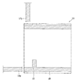
도 1은 일반적인 액정표시장치를 개략적으로 나타내는 분해사시도이다.1 is an exploded perspective view schematically showing a general liquid crystal display device.
도면에 도시된 바와 같이, 상기 액정표시장치는 크게 컬러필터 기판(5)과 박막 트랜지스터 기판(10) 및 상기 컬러필터 기판(5)과 박막 트랜지스터 기판(10) 사이에 형성된 액정층(liquid crystal layer)(30)으로 구성된다.As shown in the figure, the liquid crystal display comprises a
상기 컬러필터 기판(5)은 적(Red; R), 녹(Green; G) 및 청(Blue; B)의 색상을 구현하는 다수의 서브-컬러필터(7)로 구성된 컬러필터(C)와 상기 서브-컬러필터(7) 사이를 구분하고 액정층(30)을 투과하는 광을 차단하는 블랙매트릭스(black matrix)(6), 그리고 상기 액정층(30)에 전압을 인가하는 투명한 공통전극(8)으로 이루어져 있다.The
또한, 상기 박막 트랜지스터 기판(10)은 종횡으로 배열되어 복수개의 화소영역(P)을 정의하는 복수개의 게이트라인(16)과 데이터라인(17), 상기 게이트라인(16)과 데이터라인(17)의 교차영역에 형성된 스위칭소자인 박막 트랜지스터(T) 및 상기 화소영역(P) 위에 형성된 화소전극(18)으로 이루어져 있다.The thin
상기의 컬러필터 기판(5)과 박막 트랜지스터 기판(10)은 화상표시 영역의 외 곽에 형성된 실런트(sealant)(미도시)에 의해 대향하도록 합착되어 액정표시패널을 구성하며, 상기 컬러필터 기판(5)과 박막 트랜지스터 기판(10)의 합착은 상기 컬러필터 기판(5) 또는 박막 트랜지스터 기판(10)에 형성된 합착키(미도시)를 통해 이루어진다.The
상기 비정질 실리콘 박막 트랜지스터에 사용되는 수소화된 비정질 실리콘은 원자 배열이 무질서하기 때문에 약한 결합(week Si-Si bond) 및 댕글링 본드(dangling bond)가 존재하여 빛 조사나 전기장 인가시 준 안정상태로 변화되어 박막 트랜지스터 소자로 활용시 안정성이 문제로 대두되고 있으며, 낮은 전하이동도로는 구동회로로 이용하는데 한계가 있다.Since the hydrogenated amorphous silicon used in the amorphous silicon thin film transistor is disordered in its atomic arrangement, there is a weak bond (week Si-Si bond) and a dangling bond, Therefore, stability is a serious problem when it is used as a thin film transistor device, and a low charge transfer path is limited to use as a driving circuit.
이에 전하이동도의 증가를 통한 빠른 응답속도 및 안정성을 확보하기 위해 결정화 기술을 적용하게 된다.Therefore, the crystallization technique is applied in order to secure a fast response speed and stability by increasing the charge mobility.
도 2는 일반적인 다결정 실리콘 박막 트랜지스터의 구조를 개략적으로 나타내는 단면도이다.2 is a cross-sectional view schematically showing the structure of a general polycrystalline silicon thin film transistor.
도면에 도시된 바와 같이, 일반적인 다결정 실리콘 박막 트랜지스터는 상부 게이트(top gate) 구조로 소정의 기판(10) 위에 형성된 버퍼층(buffer layer)(11)과 액티브층(24), 상기 액티브층(24) 위에 형성된 제 1 절연막(15a), 상기 제 1 절연막(15a) 위에 형성된 게이트전극(21), 상기 게이트전극(21) 위에 형성된 제 2 절연막(15b), 상기 액티브층(24)의 소오스/드레인영역(24a, 24b)과 전기적으로 접속하는 소오스/드레인전극(22, 23), 상기 소오스/드레인전극(22, 23) 위에 형성된 제 3 절연막(15c) 및 상기 드레인전극(23)과 전기적으로 접속하는 화소전극(18)으로 이루어져 있다.As shown in the figure, a typical polycrystalline silicon thin film transistor includes a
이때, 도면부호 24c는 상기 소오스전극(22)과 드레인전극(23) 간에 전도채널(conductive channel)을 형성하는 액티브층(24)의 채널영역을 나타내며, 상기 액티브층(24)은 결정화된 다결정 실리콘 박막으로 이루어져 있다.
이하, 이와 같이 구성된 상기 다결정 실리콘 박막 트랜지스터의 제조공정을 도면을 참조하여 상세히 설명한다.Hereinafter, a manufacturing process of the polycrystalline silicon thin film transistor having such a structure will be described in detail with reference to the drawings.
도 3a 내지 도 3f는 상기 도 2에 도시된 박막 트랜지스터의 제조공정을 순차적으로 나타내는 단면도로써, n 채널의 박막 트랜지스터가 형성되는 화소부의 박막 트랜지스터를 제조하는 과정을 예를 들어 나타내고 있다3A to 3F are cross-sectional views sequentially illustrating a manufacturing process of the thin film transistor shown in FIG. 2, illustrating a process of manufacturing a thin film transistor of a pixel portion in which an n-channel thin film transistor is formed
도 3a에 도시된 바와 같이, 유리와 같은 투명한 절연물질로 이루어진 기판(10) 위에 버퍼층(11)과 비정질 실리콘 박막을 형성한 다음, 상기 비정질 실리콘 박막을 결정화하여 다결정 실리콘 박막을 형성한다. 이후, 상기 다결정 실리콘 박막을 포토리소그래피공정(제 1 마스크공정)을 이용하여 패터닝하여 상기 다결정 실리콘 박막으로 이루어진 액티브층(24)을 형성한다.As shown in FIG. 3A, a
그리고, 도 3b에 도시된 바와 같이, 상기 기판(10) 전면에 차례대로 제 1 절연막(15a)과 제 1 도전막을 형성한 후, 포토리소그래피공정(제 2 마스크공정)을 이용하여 상기 제 1 도전막을 선택적으로 패터닝함으로써 상기 액티브층(24) 위에 상기 제 1 도전막으로 이루어진 게이트전극(21)을 형성한다.3B, a first
이후, 상기 게이트전극(21)을 마스크로 상기 액티브층(24)의 소정 영역에 고농도의 n+ 이온을 주입하여 n+의 소오스영역(24a)과 드레인영역(24b)을 형성한다. 여기서, 도면부호 24c는 상기 소오스영역(24a)과 드레인영역(24b) 사이에 전도채널을 형성하는 채널영역을 의미한다.Then, high concentration n + ions are implanted into a predetermined region of the
다음으로, 도 3c에 도시된 바와 같이, 상기 기판(10) 전면에 제 2 절연막(15b)을 증착한 후, 포토리소그래피공정(제 3 마스크공정)을 통해 상기 제 1 절연막(15a)과 제 2 절연막(15b)의 일부 영역을 제거하여 상기 소오스영역(24a)의 일부를 노출시키는 제 1 콘택홀(40a)과 상기 드레인영역(24b)의 일부를 노출시키는 제 2 콘택홀(40b)을 형성한다.Next, as shown in FIG. 3C, a second
그리고, 도 3d에 도시된 바와 같이, 제 2 도전막을 기판(10) 전면에 형성한 후 포토리소그래피공정(제 4 마스크공정)을 이용하여 패터닝함으로써 상기 제 1 콘택홀(40a)을 통해 상기 소오스영역(24a)과 전기적으로 접속하는 소오스전극(22)을 형성하며, 상기 제 2 콘택홀(40b)을 통해 상기 드레인영역(24b)과 전기적으로 접속하는 드레인전극(23)을 형성한다.3D, the second conductive film is formed on the entire surface of the
다음으로, 도 3e에 도시된 바와 같이, 상기 기판(10) 전면에 제 3 절연막(15c)을 증착한 후, 포토리소그래피공정(제 5 마스크공정)을 이용하여 상기 제 3 절연막(15c)을 패터닝함으로써 상기 드레인전극(23)의 일부를 노출시키는 제 3 콘택홀(40c)을 형성한다.3E, a third
그리고, 도 3f에 도시된 바와 같이, 상기 제 3 절연막(15c)이 형성된 기판(10) 전면에 제 3 도전막을 형성한 후, 포토리소그래피공정(제 6 마스크공정)을 이용하여 상기 제 3 도전막을 선택적으로 패터닝함으로써 상기 제 3 콘택홀(40c)을 통해 상기 드레인전극(23)과 전기적으로 접속하는 화소전극(18)을 형성한다.3F, a third conductive film is formed on the entire surface of the
이와 같이 상기 다결정 실리콘 박막 트랜지스터를 포함하는 박막 트랜지스터 기판의 제조에는 최소한 6~7마스크공정이 필요하며, 상기 마스크공정은 마스크에 그려진 패턴을 박막이 증착된 기판 위에 전사시켜 원하는 패턴을 형성하는 일련의 공정으로 감광액 도포, 노광, 현상공정 등 다수의 공정으로 이루어지며, 다수의 마스크공정은 생산수율을 떨어뜨리게 한다. 특히, 패턴을 형성하기 위하여 설계된 마스크는 매우 고가이어서, 공정에 적용되는 마스크수가 증가하면 박막 트랜지스터 기판의 제조비용이 이에 비례하여 상승하게 된다.In order to manufacture the thin film transistor substrate including the polycrystalline silicon thin film transistor, at least 6 to 7 mask processes are required. In the mask process, a pattern drawn on the mask is transferred onto the substrate on which the thin film is deposited to form a desired pattern The process consists of a number of processes, such as coating of photoresist, exposure, and development, and many masking processes reduce production yield. In particular, the mask designed to form the pattern is very expensive, so that as the number of masks applied to the process increases, the manufacturing cost of the thin film transistor substrate rises accordingly.
또한, 상기 다결정 실리콘 박막 트랜지스터는 상부 게이트 구조로 형성하는 것이 일반적이므로 하부 게이트 구조인 기존의 비정질 실리콘 박막 트랜지스터의 제조라인을 이용할 수 없어 신규투자가 필요하며, 도핑과 레이저 결정화공정이 추가로 필요하여 대면적화 및 비용면에서 불리하다.In addition, since the polycrystalline silicon thin film transistor is generally formed with a top gate structure, a new investment is required because a manufacturing line of a conventional amorphous silicon thin film transistor having a bottom gate structure can not be used, and a doping and laser crystallization process is further required It is disadvantageous in terms of size and cost.
본 발명은 상기한 문제를 해결하기 위한 것으로, 다결정 실리콘을 박막 트랜지스터의 액티브층으로 사용한 하부 게이트 구조의 박막 트랜지스터 기판의 제조방법을 제공하는데 목적이 있다.It is an object of the present invention to provide a method of manufacturing a TFT having a bottom gate structure using polycrystalline silicon as an active layer of a thin film transistor.
본 발명의 다른 목적은 에치 스타퍼 구조를 채택하는 동시에 하부 게이트 구조를 사용하여 백 채널을 노출되지 않게 함으로써 소자의 신뢰성을 확보하는 한편, 상기 에치 스타퍼와 액티브층 및 패드부 콘택홀을 한번의 마스크공정으로 형성함으로써 총 4번의 마스크공정으로 박막 트랜지스터를 제작하도록 한 박막 트랜지스터 기판의 제조방법을 제공하는데 있다.Another object of the present invention is to provide a semiconductor device which adopts an etch stop structure and at the same time ensures that the back channel is not exposed by using the bottom gate structure to secure the reliability of the device, And a thin film transistor is manufactured by a total of four mask processes.
본 발명의 다른 목적 및 특징들은 후술되는 발명의 구성 및 특허청구범위에서 설명될 것이다.Other objects and features of the present invention will be described in the following description of the invention and claims.
상기한 목적을 달성하기 위하여, 본 발명의 박막 트랜지스터 기판의 제조방법은 제 1 마스크공정을 통해 화소부에 게이트전극과 게이트라인을 형성하며, 게이트패드부 및 데이터패드부에 각각 게이트패드라인 및 데이터패드라인을 형성하는 것을 특징으로 한다.
그리고, 제 2 마스크공정을 통해 상기 게이트전극 상부에 다결정 실리콘으로 이루어진 액티브층을 형성하는 동시에 상기 액티브층 위에 절연막으로 이루어진 에치 스타퍼를 형성하며, 상기 데이터패드라인의 일부를 노출시키는 제 1 콘택홀과, 상기 게이트패드라인의 일부 및 상기 데이터패드라인의 다른 일부를 노출시키는 제 2 콘택홀 및 제 3 콘택홀을 형성하는 것을 특징으로 한다. 이때, 상기 제 2 마스크공정은 다중노출 마스크를 이용하거나, 또는 하프-톤 마스크와 추가적인 애싱공정을 이용할 수 있다.
그리고, 제 3 마스크공정을 통해 상기 액티브층 상부에 n+ 비정질 실리콘으로 이루어진 소오스/드레인영역을 형성하는 동시에 소오스/드레인전극을 형성하며, 상기 제 1 콘택홀을 통해 상기 데이터패드라인의 일부와 전기적으로 접속하는 데이터라인을 형성하는 것을 특징으로 한다.
그리고, 제 4 마스크공정을 통해 상기 드레인전극과 전기적으로 접속하는 화소전극을 형성하는 것을 특징으로 한다.According to another aspect of the present invention, there is provided a method of manufacturing a thin film transistor substrate including forming a gate electrode and a gate line in a pixel portion through a first mask process, forming a gate pad line and a data pad Thereby forming a pad line.
In addition, an active layer made of polycrystalline silicon is formed on the gate electrode through a second mask process, an etch stopper made of an insulating film is formed on the active layer, a first contact hole exposing a part of the data pad line, And a second contact hole and a third contact hole exposing a part of the gate pad line and another part of the data pad line are formed. At this time, the second mask process may use a multiple exposure mask, or a half-tone mask and an additional ashing process.
In addition, a source / drain region of n + amorphous silicon is formed on the active layer through a third mask process and a source / drain electrode is formed on the active layer, and electrically connected to a portion of the data pad line through the first contact hole Thereby forming a data line to be connected.
Then, a pixel electrode electrically connected to the drain electrode is formed through a fourth mask process.
상술한 바와 같이, 본 발명에 따른 박막 트랜지스터 기판의 제조방법은 다결정 실리콘을 박막 트랜지스터의 액티브층으로 사용함에 따라 높은 전하이동도로 구동회로에 이용 가능한 효과를 제공한다.As described above, the method of manufacturing a thin film transistor substrate according to the present invention provides an effect that can be used in a high charge moving driving circuit by using polycrystalline silicon as an active layer of a thin film transistor.
또한, 본 발명에 따른 박막 트랜지스터 기판의 제조방법은 에치 스타퍼 구조를 채택하는 동시에 하부 게이트 구조를 사용하여 백 채널영역을 보호함으로써 소자의 신뢰성을 향상시키는 한편, 대면적 기판에서의 공정 균일도를 향상시킬 수 있는 효과를 제공한다.In addition, the manufacturing method of the thin film transistor substrate according to the present invention adopts the etch stop structure and protects the back channel region by using the lower gate structure, thereby improving the reliability of the device and improving the process uniformity in the large area substrate And provides an effect that can be achieved.
또한, 본 발명에 따른 박막 트랜지스터 기판의 제조방법은 상기 에치 스타퍼와 액티브층 및 패드부 콘택홀을 한번의 마스크공정으로 형성함으로써 박막 트랜지 스터의 제조에 사용되는 마스크수를 줄여 제조공정 및 비용을 절감시키는 효과를 제공한다.The method of manufacturing a thin film transistor substrate according to the present invention is characterized in that the etch stopper, the active layer and the pad portion contact holes are formed by a single mask process, thereby reducing the number of masks used in manufacturing the thin film transistor, Saving effect.
이와 같이 본 발명에 따른 박막 트랜지스터 기판의 제조방법은 하부 게이트 구조를 적용하여 마스크수를 줄임과 동시에 백 채널영역이 노출되지 않은 상태로 후속공정을 진행함으로써 신뢰성 확보와 동시에 원가 경쟁력을 확보할 수 있게 된다.As described above, according to the method of manufacturing a thin film transistor substrate according to the present invention, the number of masks is reduced by applying a bottom gate structure, and a subsequent process is performed in a state in which a back channel region is not exposed, thereby securing reliability and securing cost competitiveness do.
이하, 첨부한 도면을 참조하여 본 발명에 따른 박막 트랜지스터 기판의 제조방법의 바람직한 실시예를 상세히 설명한다.Hereinafter, preferred embodiments of a method of manufacturing a thin film transistor substrate according to the present invention will be described in detail with reference to the accompanying drawings.
도 4는 본 발명의 실시예에 따른 박막 트랜지스터 기판 일부를 개략적으로 나타내는 평면도로써, 다결정 실리콘을 액티브층으로 사용한 다결정 실리콘 박막 트랜지스터 기판 구조를 개략적으로 나타내고 있다.4 is a plan view schematically showing a part of a thin film transistor substrate according to an embodiment of the present invention, and schematically shows a substrate structure of a polycrystalline silicon thin film transistor using polycrystalline silicon as an active layer.
또한, 도 5는 본 발명의 실시예에 따른 박막 트랜지스터 기판 일부를 개략적으로 나타내는 단면도로써, 상기 도 4에 도시된 박막 트랜지스터 기판의 A-A'선과 B-B선에 따른 단면 및 도시되지 않은 링크부의 단면을 예를 들어 나타내고 있다.5 is a cross-sectional view schematically showing a part of a thin film transistor substrate according to an embodiment of the present invention. The thin film transistor substrate shown in FIG. 4 has a cross section along line A-A 'and line BB and a cross section For example.
이때, 설명의 편의를 위해 상기 도 4 및 도 5는 게이트패드부와 데이터패드부 및 화소부의 박막 트랜지스터를 포함하는 하나의 화소를 나타내고 있다. 또한, 상기 도 5는 데이터라인과 데이터패드라인이 연결되는 링크부의 일부를 포함하여 나타내고 있다.4 and 5 illustrate one pixel including a gate pad portion, a data pad portion, and a thin film transistor of the pixel portion. 5 illustrates a portion of a link portion to which a data line and a data pad line are connected.
도면에 도시된 바와 같이, 본 발명의 실시예에 따른 박막 트랜지스터 기 판(110)에는 상기 기판(110) 위에 종횡으로 배열되어 화소영역을 정의하는 게이트라인(116)과 데이터라인(117)이 형성되어 있다. 또한, 상기 게이트라인(116)과 데이터라인(117)의 교차영역에는 스위칭소자인 다결정 실리콘 박막 트랜지스터가 형성되어 있으며, 상기 화소영역 내에는 상기 다결정 실리콘 박막 트랜지스터에 연결되어 컬러필터 기판(미도시)의 공통전극과 함께 액정층(미도시)을 구동시키는 화소전극(118)이 형성되어 있다.As shown in the figure, a thin
상기 본 발명의 실시예에 따른 다결정 실리콘 박막 트랜지스터는 상기 게이트라인(116)에 연결된 게이트전극(121), 상기 데이터라인(117)에 연결된 소오스전극(122) 및 상기 화소전극(118)에 연결된 드레인전극(123)으로 구성되어 있다. 또한, 상기 다결정 실리콘 박막 트랜지스터는 상기 게이트전극(121)에 공급되는 게이트 전압에 의해 상기 소오스전극(122)과 드레인전극(123) 간에 전도채널을 형성하는 다결정 실리콘으로 이루어진 액티브층(124)을 포함한다.The polycrystalline silicon thin film transistor according to an embodiment of the present invention includes a
이때, 상기 화소전극(118)의 일부는 게이트 절연막(115a)을 사이에 두고 그 하부의 게이트라인(116)의 일부와 중첩되어 스토리지 커패시터(storage capacitor)(Cst)를 형성하게 된다. 상기 스토리지 커패시터(Cst)는 액정 커패시터에 인가된 전압을 다음 신호가 들어올 때까지 일정하게 유지시키는 역할을 한다. 이러한 스토리지 커패시터(Cst)는 신호 유지 이외에도 계조(gray scale) 표시의 안정과 플리커(flicker) 및 잔상(afterimage) 감소 등의 효과를 가진다.At this time, a part of the
또한, 상기 박막 트랜지스터 기판(110)의 가장자리 영역에는 상기 게이트라인(116)과 데이터라인(117)에 각각 전기적으로 접속하는 게이트패드전극(126p)과 데이터패드전극(127p)이 형성되어 있으며, 외부의 구동회로부(미도시)로부터 인가 받은 주사신호와 데이터신호를 각각 상기 게이트라인(116)과 데이터라인(117)에 전달하게 된다.A
즉, 상기 게이트라인(116)과 데이터라인(117)은 구동회로부 쪽으로 연장되어 각각 해당하는 게이트패드라인(116p)과 데이터패드라인(117p)에 연결되며, 상기 게이트패드라인(116p)과 데이터패드라인(117p)은 상기 게이트패드라인(116p)과 데이터패드라인(117p)에 각각 전기적으로 접속된 게이트패드전극(126p)과 데이터패드전극(127p)을 통해 구동회로부로부터 각각 주사신호와 데이터신호를 인가 받게 된다.That is, the
이때, 상기 데이터패드라인(117p)은 링크부 내에 형성된 제 1 콘택홀을 통해 데이터라인(117)에 연결되게 되며, 상기 게이트패드전극(126p)은 제 2 콘택홀(140b)을 통해 상기 게이트패드라인(116p)과 전기적으로 접속하고 상기 데이터패드전극(127p)은 제 3 콘택홀(140c)을 통해 상기 데이터패드라인(117p)과 전기적으로 접속하게 된다.The
참고로, 도면부호 125a, 125b 및 125'은 각각 n+ 비정질 실리콘으로 이루어진 소오스영역, 드레인영역 및 n+ 비정질 실리콘 박막패턴을 나타낸다. For reference,
이와 같은 특징을 가진 상기 본 발명의 실시예에 따른 다결정 실리콘 박막 트랜지스터는 상기 액티브층(124)의 백 채널(back channel)영역 위의 상기 소오스전극(122)과 드레인전극(123) 사이에 소정의 절연막으로 이루어진 에치 스타퍼(150)가 형성되게 되는데, 상기 에치 스타퍼(150)는 후속공정에 의한 백 채널영역의 손상을 방지하기 역할을 한다. 즉, 상기 본 발명의 실시예에 따른 에치 스타 퍼(150)는 상기 액티브층(124)의 백 채널영역 위에 형성되어 후속공정 진행 중에 상기 액티브층(124)의 백 채널영역이 마스크공정에 의한 화학물질과의 접촉, 습식 또는 건식식각 및 플라즈마 공정 등에 노출되는 것을 방지하는 역할을 하게 된다.The polycrystalline silicon thin film transistor according to an embodiment of the present invention having such a characteristic is formed between the
특히, 상기 본 발명의 실시예에 따른 다결정 실리콘 박막 트랜지스터는 비정질 실리콘 박막 트랜지스터의 일반적인 구조와 동일하게 하부 게이트 구조를 채택하고 있으며, 상기 에치 스타퍼(150)와 액티브층(124) 및 제 1, 제 2, 제 3 콘택홀(140b, 140c)을 다중노출 마스크 또는 하프-톤 마스크를 이용하여 한번의 마스크공정으로 형성함으로써 박막 트랜지스터 기판(110)을 제조하는데 있어 한번의 마스크수를 줄일 수 있게 된다.Particularly, the polycrystalline silicon thin film transistor according to the embodiment of the present invention adopts a lower gate structure like the general structure of the amorphous silicon thin film transistor, and the
이와 같이 본 발명의 실시예에 따른 박막 트랜지스터 기판은 다중노출 마스크, 즉 암부로 이루어진 차단영역, 모든 광을 투과시키는 제 1 투과영역, 하프-톤의 제 2 투과영역 및 하프-톤과 슬릿부가 적용된 제 3 투과영역의 멀티-톤(multi tone) 마스크를 이용한 한번의 마스크공정으로 에치 스타퍼와 액티브층 및 콘택홀을 형성함으로써 총 4번의 마스크공정을 통해 박막 트랜지스터 기판을 제작할 수 있게 되는데, 이를 다음의 박막 트랜지스터 기판의 제조방법을 통해 상세히 설명한다.As described above, the thin film transistor substrate according to the embodiment of the present invention includes a plurality of exposure masks, that is, a blocking region made up of a dark portion, a first transparent region transmitting all light, a second transparent region having a half- A thin film transistor substrate can be manufactured through a total of four mask processes by forming an etch stopper, an active layer and a contact hole by a single mask process using a multi-tone mask in a third transmission region, The manufacturing method of the thin film transistor substrate will be described in detail.
도 6a 내지 도 6d는 상기 도 4에 도시된 박막 트랜지스터 기판의 제조공정을 순차적으로 나타내는 평면도이다.6A to 6D are plan views sequentially illustrating the manufacturing process of the thin film transistor substrate shown in FIG.
또한, 도 7a 내지 도 7d는 상기 도 5에 도시된 박막 트랜지스터 기판의 제조공정을 순차적으로 나타내는 단면도이다.7A to 7D are cross-sectional views sequentially illustrating a manufacturing process of the thin film transistor substrate shown in FIG.
도 6a 및 도 7a에 도시된 바와 같이, 투명한 절연물질로 이루어진 기판(110)이 화소부에 게이트전극(121)과 게이트라인(116)을 형성하며, 게이트패드부 및 데이터패드부에 각각 게이트패드라인(116p) 및 데이터패드라인(117p)을 형성한다.6A and 7A, a
이때, 상기 게이트전극(121), 게이트라인(116), 게이트패드라인(116p) 및 데이터패드라인(117p)은 위에 제 1 도전막을 상기 기판(110) 전면에 증착한 후 포토리소그래피공정(제 1 마스크공정)을 통해 선택적으로 패터닝하여 형성하게 된다.The
여기서, 상기 제 1 도전막으로 알루미늄(aluminium; Al), 알루미늄 합금(Al alloy), 텅스텐(tungsten; W), 구리(copper; Cu), 니켈(nickel; Ni), 크롬(chromium; Cr), 몰리브덴(molybdenum; Mo), 티타늄(titanium; Ti), 백금(platinum; Pt), 탄탈(tantalum; Ta) 등과 같은 저저항 불투명 도전물질을 사용할 수 있다. 또한, 상기 제 1 도전막은 인듐-틴-옥사이드(Indium Tin Oxide; ITO), 인듐-징크-옥사이드(Indium Zinc Oxide; IZO)와 같은 투명한 도전물질을 사용할 수 있으며, 상기 도전물질이 2가지 이상 적층된 다층구조로 형성할 수도 있다.Here, the first conductive layer may be formed of one selected from the group consisting of aluminum (Al), aluminum alloy (Al alloy), tungsten (W), copper (Cu), nickel (Ni), chromium A low resistance opaque conductive material such as molybdenum (Mo), titanium (Ti), platinum (Pt), tantalum (Ta) The first conductive layer may be formed of a transparent conductive material such as indium tin oxide (ITO), indium zinc oxide (IZO), or the like. Layer structure.
다음으로, 도 6b 및 도 7b에 도시된 바와 같이, 상기 게이트전극(121), 게이트라인(116), 게이트패드라인(116p) 및 데이터패드라인(117p)이 형성된 기판(110) 전면에 게이트 절연막(115a)과 비정질 실리콘 박막 및 절연막을 형성한 후, 엑시머 레이저 결정화나 전자빔(e-beam) 등의 결정화공정을 거쳐 상기 비정질 실리콘 박막을 다결정 실리콘 박막으로 결정화한다.6B and 7B, on the entire surface of the
이후, 포토리소그래피공정(제 2 마스크공정)을 통해 선택적으로 패터닝함으로써 상기 게이트전극(121) 상부에 상기 다결정 실리콘으로 이루어진 액티브 층(124)을 형성하며, 상기 액티브층(124)의 백 채널영역 위에 상기 절연막으로 이루어진 에치 스타퍼(150)를 형성한다.Thereafter, an
상기 에치 스타퍼(150)는 상기 액티브층(124)의 백 채널영역 위에 아일랜드 형태로 형성됨으로써 후술할 공정에서 소오스/드레인전극을 패터닝할 때 박막 트랜지스터의 백 채널이 손상 받는 것을 방지하게 된다.The
이때, 상기 기판(110)의 링크부에는 상기 게이트 절연막(115a)의 일부영역이 제거되어 상기 데이터패드라인(117p)의 일부를 노출시키는 제 1 콘택홀(140a)이 형성되게 되며, 상기 기판(110)의 패드부에는 상기 게이트 절연막(115a)의 일부영역이 제거되어 각각 상기 게이트패드라인(116p) 및 데이터패드라인(117p)의 일부를 노출시키는 제 2 콘택홀(140b) 및 제 3 콘택홀(140c)이 형성되게 된다.A portion of the
여기서, 상기 본 발명의 실시예에 따른 상기 액티브층(124)과 에치 스타퍼(150) 및 콘택홀(140a~140c)은 다중노출 마스크 또는 하프-톤 마스크와 애싱(ashing)공정을 이용한 한번의 마스크공정(제 2 마스크공정)으로 동시에 형성하게 되는데, 이하 도면을 참조하여 상기 제 2 마스크공정을 상세히 설명한다.Here, the
도 8a 내지 도 8i는 상기 도 6b 및 도 7b에 도시된 본 발명의 실시예에 따른 제 2 마스크공정을 구체적으로 나타내는 단면도로써, 다중노출 마스크를 이용한 제 2 마스크공정을 나타내고 있다.FIGS. 8A to 8I are cross-sectional views illustrating a second mask process according to an embodiment of the present invention shown in FIGS. 6B and 7B, which is a second mask process using a multiple exposure mask.
도 8a에 도시된 바와 같이, 상기 게이트전극(121), 게이트라인(116), 게이트패드라인(116p) 및 데이터패드라인(117p)이 형성된 기판(110) 전면에 게이트 절연막(115a)과 비정질 실리콘 박막(120') 및 절연막(130)을 형성한다.8A, a
이때, 상기 게이트 절연막(115a)과 절연막(130)은 실리콘질화막(SiNx), 실리콘산화막(SiO2)과 같은 무기절연막 또는 하프늄(hafnium; Hf) 옥사이드, 알루미늄 옥사이드와 같은 고유전성 산화막으로 이루어질 수 있다.In this case, the gate insulating film (115a) and an insulating
그리고, 상기 게이트 절연막(115a)과 절연막(130)은 플라즈마 화학기상증착(Plasma Enhanced Chemical Vapour Deposition; PECVD) 장비를 이용한 CVD방법으로 형성하거나 스퍼터 장비를 이용한 물리기상증착(Physical Vapour Deposition; PVD)방법으로 형성할 수 있다.The
다음으로, 도 8b에 도시된 바와 같이, 소정의 결정화공정을 진행하여 상기 비정질 실리콘 박막(120')을 다결정 실리콘 박막(120)으로 결정화한다.Next, as shown in FIG. 8B, a predetermined crystallization process is performed to crystallize the amorphous silicon thin film 120 'into a polycrystalline silicon
여기서, 상기 비정질 실리콘 박막(120')을 형성하는 대표적인 방법으로는 저압 화학기상증착(Low Pressure Chemical Vapor Deposition; LPCVD)방법과 플라즈마 화학기상증착방법이 있다. 또한, 상기 비정질 실리콘 박막(120')의 결정화로 여러 가지 결정화방법을 이용할 수 있으며, 레이저를 이용하는 레이저 어닐링방법을 이용하는 경우에는 펄스(pulse) 형태의 레이저를 이용한 엑시머 레이저 어닐링(Eximer Laser Annealing; ELA)방법이 주로 이용되나, 그레인(grain)을 수평방향으로 성장시켜 결정화특성을 향상시킨 순차적 수평결정화(Sequential Lateral Solidification; SLS)방법을 이용할 수도 있다.Here, typical methods for forming the amorphous silicon thin film 120 'include a low pressure chemical vapor deposition (LPCVD) method and a plasma chemical vapor deposition method. In addition, various crystallization methods can be used for the crystallization of the amorphous silicon thin film 120 '. In the case of using a laser annealing method using a laser, excimer laser annealing (ELA) using a pulse- ) Method is mainly used, but it is also possible to use a sequential lateral solidification (SLS) method in which grains are grown in a horizontal direction to improve crystallization characteristics.
그리고, 도 8c에 도시된 바와 같이, 상기 기판(110) 전면에 포토레지스트와 같은 감광성물질로 이루어진 감광막(170)을 형성한 후, 본 발명의 실시예에 따른 다중노출 마스크(180)를 통해 상기 감광막(170)에 선택적으로 광을 조사한다.8C, a
이때, 상기 다중노출 마스크(180)에는 조사된 광을 모두 투과시키는 제 1 투과영역(I)과 광의 일부만 투과시키고 일부는 차단하기 위해 하프-톤 부로 이루어진 제 2 투과영역(II)과 하프-톤 부와 슬릿부로 이루어진 제 3 투과영역(III) 및 조사된 모든 광을 차단하는 차단영역(IV)이 마련되어 있으며, 상기 다중노출 마스크(180)를 투과한 광만이 상기 감광막(170)에 조사되게 된다.At this time, the
이어서, 상기 다중노출 마스크(180)를 통해 노광된 상기 감광막(170)을 현상하고 나면, 도 8d에 도시된 바와 같이, 상기 차단영역(IV)과 제 2 투과영역(II) 및 제 3 투과영역(III)을 통해 광이 모두 차단되거나 일부만 차단된 영역에는 소정 두께의 제 1 감광막패턴(170a) 내지 제 4 감광막패턴(170d)이 남아있게 되고, 모든 광이 투과된 제 1 투과영역(I)에는 상기 감광막이 완전히 제거되어 상기 절연막(130) 표면이 노출되게 된다.8D, after the
이때, 상기 차단영역(IV)에 형성된 제 1 감광막패턴(170a)은 상기 제 2 투과영역(II)과 제 3 투과영역(III)을 통해 형성된 제 2 감광막패턴(170b) 내지 제 4 감광막패턴(170d)보다 두껍게 형성된다. 또한, 상기 제 3 투과영역(III)을 통해 형성된 상기 제 2 감광막패턴(170b)과 제 3 감광막패턴(170c)은 상기 제 2 투과영역(II)을 통해 형성된 상기 제 4 감광막패턴(170d)보다 두껍게 형성되며, 상기 제 1 투과영역(I)을 통해 광이 모두 투과된 영역에는 상기 감광막이 완전히 제거되는데, 이것은 포지티브 타입의 포토레지스트를 사용했기 때문이며, 본 발명이 이에 한정되는 것은 아니며 네거티브 타입의 포토레지스트를 사용하여도 무방하다.The
다음으로, 도 8e에 도시된 바와 같이, 상기와 같이 형성된 제 1 감광막패턴(170a) 내지 제 4 감광막패턴(170d)을 마스크로 하여, 그 하부에 형성된 게이트 절연막(115a), 다결정 실리콘 박막(120) 및 절연막(130)을 선택적으로 제거하게 되면, 상기 기판(110)의 링크부에 상기 데이터패드라인(117p)의 일부를 노출시키는 제 1 콘택홀(140a)이 형성되며, 상기 기판(110)의 패드부에 각각 상기 게이트패드라인(116p) 및 데이터패드라인(117p)의 일부를 노출시키는 제 2 콘택홀(140b) 및 제 3 콘택홀(140c)이 형성되게 된다.Next, as shown in FIG. 8E, using the
이후, 상기 제 1 감광막패턴(170a) 내지 제 4 감광막패턴(170d)의 두께 일부를 제거하는 애싱공정을 진행하게 되면, 도 8f에 도시된 바와 같이, 상기 제 2 투과영역(II)의 제 4 감광막패턴이 완전히 제거되게 된다.As shown in FIG. 8F, when the ashing process for removing a part of the thicknesses of the first to
이때, 상기 제 1 감광막패턴 내지 제 3 감광막패턴은 상기 제 4 감광막패턴의 두께만큼이 제거된 제 5 감광막패턴(170a') 내지 제 7 감광막패턴(170c')으로 상기 차단영역(IV)과 제 3 투과영역(III)에 대응하는 소오스영역과 드레인영역 및 상기 소오스영역과 드레인영역 사이의 채널영역에만 남아있게 된다.At this time, the first to third photoresist patterns to the fourth to the
이후, 도 8g에 도시된 바와 같이, 상기 남아있는 제 5 감광막패턴(170a') 내지 제 7 감광막패턴(170c')을 마스크로 하여 그 하부에 형성된 다결정 실리콘 박막과 절연막을 선택적으로 제거하게 되면, 상기 기판(110)의 화소부에 상기 다결정 실리콘으로 이루어진 액티브층(124)이 형성되게 된다.8G, if the polycrystalline silicon thin film and the insulating film formed therebelow are selectively removed using the remaining
이때, 상기 액티브층(124) 상부에는 상기 절연막으로 이루어지며 상기 액티브층(124)과 실질적으로 동일한 형태로 패터닝된 절연막패턴(130')이 형성되게 된 다.At this time, an insulating film pattern 130 'formed of the insulating film and patterned in substantially the same shape as the
이후, 상기 제 5 감광막패턴(170a') 내지 제 7 감광막패턴(170c')의 두께 일부를 제거하는 애싱공정을 진행하게 되면, 도 8h에 도시된 바와 같이, 상기 제 3 투과영역(III)의 제 6 감광막패턴과 제 7 감광막패턴이 완전히 제거되게 된다.8H, when the ashing process for removing a part of the thickness of the
이때, 상기 제 5 감광막패턴은 상기 제 6 감광막패턴과 제 7 감광막패턴의 두께만큼이 제거된 제 8 감광막패턴(170a")으로 상기 차단영역(III)에 대응하는 채널영역에만 남아있게 된다.At this time, the fifth photoresist pattern is the
이후, 도 8i에 도시된 바와 같이, 상기 남아있는 제 8 감광막패턴(170a")을 마스크로 하여 상기 절연막의 일부영역을 선택적으로 제거함으로써 상기 액티브층(124) 상부에 상기 절연막으로 이루어지며 상기 액티브층(124)의 채널영역을 보호하는 에치 스타퍼(150)가 형성되게 된다.8I, a portion of the insulating film is selectively removed using the remaining eighth
이와 같이 본 발명의 실시예에 따른 액티브층(124)과 에치 스타퍼(150) 및 콘택홀(140a~140c)은 다중노출 마스크를 이용함으로써 한번의 마스크공정을 통해 형성할 수 있게 된다. 그 결과 박막 트랜지스터의 제조에 사용되는 마스크수를 줄여 제조공정 및 비용이 절감되는 효과를 제공하게 된다.As described above, the
또한, 본 발명의 실시예에 따른 박막 트랜지스터는 상기 액티브층(124)의 백 채널영역이 노출되지 않게 상기 에치 스타퍼(150)를 형성하여 보호함으로써 상기 액티브층(124)의 두께를 상대적으로 얇게 할 수 있으며, 상기 액티브층(124)의 백 채널영역이 오염되는 것을 방지할 수 있게 된다. 그 결과 상기 액티브층(124)과 게이트 절연막(115a)의 두께를 얇게 할 수 있어 실질적으로 박막 트랜지스터의 구동 전압과 문턱전압이 낮아지는 효과를 얻을 수 있다.In addition, the thin film transistor according to the embodiment of the present invention forms and protects the
한편, 전술한 바와 같이 상기 액티브층과 에치 스타퍼 및 콘택홀은 하프-톤 마스크와 추가적인 애싱공정을 이용함으로써 한번의 마스크공정을 통해 형성할 수도 있는데, 이를 다음의 도면을 참조하여 상세히 설명한다.Meanwhile, as described above, the active layer, the etch stopper, and the contact hole may be formed through a single mask process by using a half-tone mask and an additional ashing process, which will be described in detail with reference to the following drawings.
도 9a 내지 도 9i는 상기 도 6b 및 도 7b에 도시된 본 발명의 실시예에 따른 다른 제 2 마스크공정을 구체적으로 나타내는 단면도로써, 하프-톤 마스크와 애싱공정을 이용한 제 2 마스크공정을 나타내고 있다.FIGS. 9A to 9I are cross-sectional views illustrating another second mask process according to an embodiment of the present invention shown in FIGS. 6B and 7B, and show a second mask process using a half-tone mask and an ashing process .
도 9a에 도시된 바와 같이, 게이트전극(221), 게이트라인(216), 게이트패드라인(216p) 및 데이터패드라인(217p)이 형성된 기판(210) 전면에 게이트 절연막(215a)과 비정질 실리콘 박막(220') 및 절연막(230)을 형성한다.9A, a
그리고, 도 9b에 도시된 바와 같이, 레이저 결정화나 전자빔 등의 결정화공정을 진행하여 상기 비정질 실리콘 박막(220')을 다결정 실리콘 박막(220)으로 결정화한다.Then, as shown in FIG. 9B, the amorphous silicon thin film 220 'is crystallized into the polycrystalline silicon
그리고, 도 9c에 도시된 바와 같이, 상기 기판(210) 전면에 포토레지스트와 같은 감광성물질로 이루어진 감광막(270)을 형성한 후, 본 발명의 실시예에 따른 하프-톤 마스크(280)를 통해 상기 감광막(270)에 선택적으로 광을 조사한다.9C, a
이때, 상기 하프-톤 마스크(280)에는 조사된 광을 모두 투과시키는 제 1 투과영역(I)과 광의 일부만 투과시키고 일부는 차단하는 제 2 투과영역(II) 및 조사된 모든 광을 차단하는 차단영역(III)이 마련되어 있으며, 상기 하프-톤 마스크(280)를 투과한 광만이 상기 감광막(270)에 조사되게 된다.At this time, the half-
이어서, 상기 하프-톤 마스크(280)를 통해 노광된 상기 감광막(270)을 현상하고 나면, 도 9d에 도시된 바와 같이, 상기 차단영역(III)과 제 2 투과영역(II)을 통해 광이 모두 차단되거나 일부만 차단된 영역에는 소정 두께의 제 1 감광막패턴(270a)과 제 2 감광막패턴(270b)이 남아있게 되고, 모든 광이 투과된 제 1 투과영역(I)에는 상기 감광막이 완전히 제거되어 상기 절연막(230) 표면이 노출되게 된다.After the
이때, 상기 차단영역(III)에 형성된 제 1 감광막패턴(270a)은 상기 제 2 투과영역(II)을 통해 형성된 제 2 감광막패턴(270b)보다 두껍게 형성된다. 또한, 상기 제 1 투과영역(I)을 통해 광이 모두 투과된 영역에는 상기 감광막이 완전히 제거되는데, 이것은 포지티브 타입의 포토레지스트를 사용했기 때문이며, 본 발명이 이에 한정되는 것은 아니며 네거티브 타입의 포토레지스트를 사용하여도 무방하다.At this time, the
다음으로, 도 9e에 도시된 바와 같이, 상기와 같이 형성된 제 1 감광막패턴(270a)과 제 2 감광막패턴(270b)을 마스크로 하여, 그 하부에 형성된 게이트 절연막(215a), 다결정 실리콘 박막(220) 및 절연막(230)을 선택적으로 제거하게 되면, 상기 기판(210)의 링크부에 상기 데이터패드라인(217p)의 일부를 노출시키는 제 1 콘택홀(240a)이 형성되며, 상기 기판(210)의 패드부에 각각 상기 게이트패드라인(216p) 및 데이터패드라인(217p)의 일부를 노출시키는 제 2 콘택홀(240b) 및 제 3 콘택홀(240c)이 형성되게 된다.9E, using the
이후, 상기 제 1 감광막패턴(270a)과 제 2 감광막패턴(270b)의 두께 일부를 제거하는 애싱공정을 진행하게 되면, 도 9f에 도시된 바와 같이, 상기 제 2 투과영 역(II)의 제 2 감광막패턴이 완전히 제거되게 된다.Then, ashing process for removing a part of the thickness of the
이때, 상기 제 1 감광막패턴은 상기 제 2 감광막패턴의 두께만큼이 제거된 제 3 감광막패턴(270a')으로 상기 차단영역(III)에 대응하는 소오스영역과 드레인영역 및 상기 소오스영역과 드레인영역 사이의 채널영역에만 남아있게 된다.At this time, the first photoresist pattern is formed by the
이후, 도 9g에 도시된 바와 같이, 상기 남아있는 제 3 감광막패턴(270a')을 마스크로 하여 그 하부에 형성된 다결정 실리콘 박막과 절연막을 선택적으로 제거하게 되면, 상기 기판(210)의 화소부에 상기 다결정 실리콘으로 이루어진 액티브층(224)이 형성되게 된다.9G, when the polycrystalline silicon thin film and the insulating film formed therebelow are selectively removed using the remaining
이때, 상기 액티브층(224) 상부에는 상기 절연막으로 이루어지며 상기 액티브층(224)과 실질적으로 동일한 형태로 패터닝된 절연막패턴(230')이 형성되게 된다.At this time, the insulating layer pattern 230 'formed of the insulating layer and patterned in substantially the same shape as the
이후, 상기 제 3 감광막패턴(270a')의 두께 일부를 제거하는 애싱공정을 진행하게 되면, 도 9h에 도시된 바와 같이, 그 폭 일부도 함께 제거되어 소정 형태의 제 4 감광막패턴(270a")으로 채널영역에만 남아있게 된다.9H, a part of the width of the
이후, 도 9i에 도시된 바와 같이, 상기 남아있는 제 4 감광막패턴(270a")을 마스크로 하여 상기 절연막의 일부영역을 선택적으로 제거함으로써 상기 액티브층(224) 상부에 상기 절연막으로 이루어지며 상기 액티브층(224)의 채널영역을 보호하는 에치 스타퍼(250)가 형성되게 된다.Thereafter, as shown in FIG. 9I, the
다음으로, 도 6c 및 도 7c에 도시된 바와 같이, 상기 액티브층(124)과 에치 스타퍼(150)가 형성된 기판(110) 전면에 n+ 비정질 실리콘 박막과 제 2 도전막을 증착한 후, 포토리소그래피공정(제 3 마스크공정)을 통해 선택적으로 패터닝함으로써 상기 기판(110)의 화소부에 상기 n+ 비정질 실리콘으로 이루어진 소오스/드레인영역(125a, 125b)을 형성하는 동시에 상기 기판(110)의 링크부에 상기 n+ 비정질 실리콘으로 이루어진 n+ 비정질 실리콘 박막패턴(125')을 형성하게 된다.Next, as shown in FIGS. 6C and 7C, after the n + amorphous silicon thin film and the second conductive film are deposited on the entire surface of the
이때, 상기 제 3 마스크공정을 통해 상기 기판(110)의 화소부에 상기 제 2 도전막으로 이루어지며 상기 소오스/드레인영역(125a, 125b)과 전기적으로 접속하는 소오스/드레인전극(122, 123)을 형성하게 된다.At this time, source /
또한, 상기 제 3 마스크공정을 통해 상기 제 2 도전막으로 이루어지며, 상기 게이트라인(116)과 교차하여 화소영역을 정의하는 데이터라인(117)을 형성하게 된다. 이때, 상기 데이터라인(117)과 n+ 비정질 실리콘 박막패턴(125')은 상기 링크부에서 상기 제 1 콘택홀(140a)을 통해 그 하부의 데이터패드라인(117p)과 전기적으로 접속하게 된다.In addition, the
이때, 상기 제 2 도전막은 소오스전극과 드레인전극 및 데이터라인을 형성하기 위해 알루미늄, 알루미늄 합금, 텅스텐, 구리, 니켈, 크롬, 몰리브덴, 티타늄, 백금, 탄탈 등과 같은 저저항 불투명 도전물질을 사용할 수 있다. 또한, 상기 제 2 도전막은 인듐-틴-옥사이드, 인듐-징크-옥사이드와 같은 투명한 도전물질을 사용할 수 있으며, 상기 도전물질이 2가지 이상 적층된 다층구조로 형성할 수도 있다.The second conductive layer may be a low resistance opaque conductive material such as aluminum, aluminum alloy, tungsten, copper, nickel, chromium, molybdenum, titanium, platinum or tantalum to form a source electrode, a drain electrode and a data line . The second conductive layer may be formed of a transparent conductive material such as indium-tin-oxide or indium-zinc-oxide, or may have a multilayer structure in which two or more conductive materials are stacked.
다음으로, 도 6d 및 도 7d에 도시된 바와 같이, 상기 소오스전극(122)과 드레인전극(123) 및 데이터라인(117)이 형성된 기판(110) 전면에 제 3 도전막을 형성한 후, 포토리소그래피공정(제 4 마스크공정)을 통해 선택적으로 제거함으로써 상 기 기판(110)의 화소부에 상기 제 3 도전막으로 이루어지며 상기 드레인전극(123)과 전기적으로 접속하는 화소전극(118)을 형성하게 된다.6D and 7D, a third conductive layer is formed on the entire surface of the
또한, 상기 제 4 마스크공정을 통해 상기 제 3 도전막으로 이루어지며, 각각 상기 제 2 콘택홀(140b) 및 제 3 콘택홀(140c)을 통해 상기 게이트패드라인(116p) 및 데이터패드라인(117p)과 전기적으로 접속하는 게이트패드전극(126p) 및 데이터패드전극(127p)을 형성하게 된다.The third conductive film is formed through the fourth mask process and is electrically connected to the
이때, 상기 제 3 도전막은 화소전극과 게이트패드전극 및 데이터패드전극을 구성하기 위해 인듐-틴-옥사이드 또는 인듐-징크-옥사이드와 같은 투과율이 뛰어난 투명한 도전물질을 포함한다.Here, the third conductive layer includes a transparent conductive material having a high transmittance such as indium-tin-oxide or indium-zinc-oxide to form a pixel electrode, a gate pad electrode, and a data pad electrode.
이와 같이 제작된 상기 본 발명의 실시예에 따른 박막 트랜지스터 기판은 화상표시 영역의 외곽에 형성된 실런트에 의해 컬러필터 기판과 대향하여 합착되게 되는데, 이때 상기 컬러필터 기판에는 상기 박막 트랜지스터와 게이트라인 및 데이터라인으로 빛이 새는 것을 방지하는 블랙매트릭스와 적, 녹 및 청색의 컬러를 구현하기 위한 컬러필터가 형성되어 있다.The thin film transistor substrate according to an embodiment of the present invention fabricated as described above is adhered to the color filter substrate opposite to the color filter substrate by a sealant formed on the outer side of the image display area. A black matrix for preventing light from leaking into the line, and a color filter for realizing red, green and blue colors are formed.
이때, 상기 컬러필터 기판과 박막 트랜지스터 기판의 합착은 상기 컬러필터 기판 또는 박막 트랜지스터 기판에 형성된 합착키를 통해 이루어진다.At this time, the color filter substrate and the thin film transistor substrate are bonded together through a covalent key formed on the color filter substrate or the thin film transistor substrate.
전술한 바와 같이 본 발명은 액정표시장치뿐만 아니라 박막 트랜지스터를 이용하여 제작하는 다른 표시장치, 예를 들면 구동 트랜지스터에 유기전계발광소자가 연결된 유기전계발광 디스플레이장치에도 이용될 수 있다.As described above, the present invention can be applied not only to liquid crystal display devices but also to other display devices manufactured using thin film transistors, for example, organic electroluminescent display devices in which organic electroluminescent devices are connected to driving transistors.
상기한 설명에 많은 사항이 구체적으로 기재되어 있으나 이것은 발명의 범위 를 한정하는 것이라기보다 바람직한 실시예의 예시로서 해석되어야 한다. 따라서 발명은 설명된 실시예에 의하여 정할 것이 아니고 특허청구범위와 특허청구범위에 균등한 것에 의하여 정하여져야 한다.While a great many are described in the foregoing description, it should be construed as an example of preferred embodiments rather than limiting the scope of the invention. Therefore, the invention should not be construed as limited to the embodiments described, but should be determined by equivalents to the appended claims and the claims.
도 1은 일반적인 액정표시장치를 개략적으로 나타내는 분해사시도.1 is an exploded perspective view schematically showing a general liquid crystal display device.
도 2는 일반적인 다결정 실리콘 박막 트랜지스터의 구조를 개략적으로 나타내는 단면도.2 is a cross-sectional view schematically showing a structure of a general polycrystalline silicon thin film transistor.
도 3a 내지 도 3f는 상기 도 2에 도시된 박막 트랜지스터의 제조공정을 순차적으로 나타내는 단면도.FIGS. 3A to 3F are cross-sectional views sequentially illustrating a manufacturing process of the thin film transistor shown in FIG. 2; FIG.
도 4는 본 발명의 실시예에 따른 박막 트랜지스터 기판 일부를 개략적으로 나타내는 평면도.4 is a plan view schematically showing a part of a thin film transistor substrate according to an embodiment of the present invention.
도 5는 본 발명의 실시예에 따른 박막 트랜지스터 기판 일부를 개략적으로 나타내는 단면도.5 is a cross-sectional view schematically showing a part of a thin film transistor substrate according to an embodiment of the present invention.
도 6a 내지 도 6d는 상기 도 4에 도시된 박막 트랜지스터 기판의 제조공정을 순차적으로 나타내는 평면도.6A to 6D are plan views sequentially showing a manufacturing process of the thin film transistor substrate shown in FIG.
도 7a 내지 도 7d는 상기 도 5에 도시된 박막 트랜지스터 기판의 제조공정을 순차적으로 나타내는 단면도.7A to 7D are cross-sectional views sequentially showing a manufacturing process of the thin film transistor substrate shown in FIG.
도 8a 내지 도 8i는 상기 도 6b 및 도 7b에 도시된 본 발명의 실시예에 따른 제 2 마스크공정을 구체적으로 나타내는 단면도.8A to 8I are cross-sectional views illustrating a second mask process according to an embodiment of the present invention shown in FIGS. 6B and 7B.
도 9a 내지 도 9i는 상기 도 6b 및 도 7b에 도시된 본 발명의 실시예에 따른 다른 제 2 마스크공정을 구체적으로 나타내는 단면도.FIGS. 9A to 9I are cross-sectional views illustrating another second mask process according to the embodiment of the present invention shown in FIGS. 6B and 7B. FIG.
** 도면의 주요부분에 대한 부호의 설명 **DESCRIPTION OF REFERENCE NUMERALS
110 : 기판 116 : 게이트라인110: substrate 116: gate line
116p : 게이트패드라인 117 : 데이터라인116p: gate pad line 117: data line
117p : 데이터패드라인 118 : 화소전극117p: data pad line 118: pixel electrode
121 : 게이트전극 122 : 소오스전극121: gate electrode 122: source electrode
123 : 드레인전극 124 : 액티브층123: drain electrode 124: active layer
126p : 게이트패드전극 127p : 데이터패드전극126p:
150 : 에치 스타퍼150: Etch Starper
Claims (9)
Priority Applications (1)
| Application Number | Priority Date | Filing Date | Title |
|---|---|---|---|
| KR1020090113480A KR101626362B1 (en) | 2009-11-23 | 2009-11-23 | Method of fabricating substrate for thin film transistor |
Applications Claiming Priority (1)
| Application Number | Priority Date | Filing Date | Title |
|---|---|---|---|
| KR1020090113480A KR101626362B1 (en) | 2009-11-23 | 2009-11-23 | Method of fabricating substrate for thin film transistor |
Publications (2)
| Publication Number | Publication Date |
|---|---|
| KR20110056963A KR20110056963A (en) | 2011-05-31 |
| KR101626362B1 true KR101626362B1 (en) | 2016-06-02 |
Family
ID=44365249
Family Applications (1)
| Application Number | Title | Priority Date | Filing Date |
|---|---|---|---|
| KR1020090113480A Active KR101626362B1 (en) | 2009-11-23 | 2009-11-23 | Method of fabricating substrate for thin film transistor |
Country Status (1)
| Country | Link |
|---|---|
| KR (1) | KR101626362B1 (en) |
Cited By (1)
| Publication number | Priority date | Publication date | Assignee | Title |
|---|---|---|---|---|
| US10297617B2 (en) | 2016-09-30 | 2019-05-21 | Samung Display Co., Ltd. | Display device and manufacturing method thereof |
Families Citing this family (2)
| Publication number | Priority date | Publication date | Assignee | Title |
|---|---|---|---|---|
| KR102281300B1 (en) | 2013-09-11 | 2021-07-26 | 삼성디스플레이 주식회사 | Thin film transistor, method of manufacturing the same, and display device including the same |
| KR102450856B1 (en) * | 2015-12-30 | 2022-10-05 | 엘지디스플레이 주식회사 | Display panel and display device having the same |
Family Cites Families (3)
| Publication number | Priority date | Publication date | Assignee | Title |
|---|---|---|---|---|
| KR20080054783A (en) * | 2006-12-13 | 2008-06-19 | 엘지디스플레이 주식회사 | Thin film transistor array substrate and manufacturing method thereof |
| KR100841371B1 (en) * | 2006-12-19 | 2008-06-26 | 삼성에스디아이 주식회사 | Thin film transistor and method of manufacturing same |
| KR20080062124A (en) * | 2006-12-29 | 2008-07-03 | 엘지디스플레이 주식회사 | Thin film transistor substrate and manufacturing method thereof |
-
2009
- 2009-11-23 KR KR1020090113480A patent/KR101626362B1/en active Active
Cited By (1)
| Publication number | Priority date | Publication date | Assignee | Title |
|---|---|---|---|---|
| US10297617B2 (en) | 2016-09-30 | 2019-05-21 | Samung Display Co., Ltd. | Display device and manufacturing method thereof |
Also Published As
| Publication number | Publication date |
|---|---|
| KR20110056963A (en) | 2011-05-31 |
Similar Documents
| Publication | Publication Date | Title |
|---|---|---|
| KR101783352B1 (en) | Flat panel display apparatus and manufacturing method of the same | |
| US7553711B2 (en) | Method for fabricating a thin film transistor for use with a flat panel display device | |
| US20100277659A1 (en) | Liquid crystal display and fabrication method thereof | |
| US20120146017A1 (en) | Oxide thin film transistor and method of fabricating the same | |
| US8283220B2 (en) | Liquid crystal display device and fabrication method thereof | |
| KR101073403B1 (en) | Liquid crystal display device and method of fabricating thereof | |
| KR20110056962A (en) | Method of manufacturing thin film transistor substrate | |
| US8357937B2 (en) | Thin film transistor liquid crystal display device | |
| KR101626362B1 (en) | Method of fabricating substrate for thin film transistor | |
| KR101141534B1 (en) | Liquid crystal display device and method of fabricating thereof | |
| KR101201707B1 (en) | Liquid crystal display device and method of fabricating the same | |
| JP4312179B2 (en) | Liquid crystal display element and manufacturing method thereof | |
| KR101631616B1 (en) | Thin film transistor and method of fabricating thereof | |
| KR101408257B1 (en) | Liquid crystal display device and manufacturing method thereof | |
| CN101207092B (en) | Liquid crystal display device and manufacturing method thereof | |
| KR101048998B1 (en) | LCD and its manufacturing method | |
| KR101856209B1 (en) | Tft of liquid crystal display device and method of fabricating the same | |
| US7932979B2 (en) | Method for fabricating a liquid crystal display device wherein the storage electrode is simultaneously formed with the active pattern | |
| KR101266274B1 (en) | Liquid crystal display device and method of fabricating the same | |
| KR101186518B1 (en) | Method of fabricating liquid crystal display device | |
| KR20080057034A (en) | LCD and its manufacturing method | |
| KR20080056569A (en) | LCD and its manufacturing method | |
| KR20070072106A (en) | LCD and its manufacturing method | |
| KR20080062930A (en) | LCD and its manufacturing method |
Legal Events
| Date | Code | Title | Description |
|---|---|---|---|
| PA0109 | Patent application |
Patent event code: PA01091R01D Comment text: Patent Application Patent event date: 20091123 |
|
| PG1501 | Laying open of application | ||
| A201 | Request for examination | ||
| PA0201 | Request for examination |
Patent event code: PA02012R01D Patent event date: 20141124 Comment text: Request for Examination of Application Patent event code: PA02011R01I Patent event date: 20091123 Comment text: Patent Application |
|
| E902 | Notification of reason for refusal | ||
| PE0902 | Notice of grounds for rejection |
Comment text: Notification of reason for refusal Patent event date: 20151030 Patent event code: PE09021S01D |
|
| E701 | Decision to grant or registration of patent right | ||
| PE0701 | Decision of registration |
Patent event code: PE07011S01D Comment text: Decision to Grant Registration Patent event date: 20160523 |
|
| GRNT | Written decision to grant | ||
| PR0701 | Registration of establishment |
Comment text: Registration of Establishment Patent event date: 20160526 Patent event code: PR07011E01D |
|
| PR1002 | Payment of registration fee |
Payment date: 20160527 End annual number: 3 Start annual number: 1 |
|
| PG1601 | Publication of registration | ||
| FPAY | Annual fee payment |
Payment date: 20190417 Year of fee payment: 4 |
|
| PR1001 | Payment of annual fee |
Payment date: 20190417 Start annual number: 4 End annual number: 4 |
|
| PR1001 | Payment of annual fee |
Payment date: 20200422 Start annual number: 5 End annual number: 5 |
|
| PR1001 | Payment of annual fee |
Payment date: 20210415 Start annual number: 6 End annual number: 6 |
|
| PR1001 | Payment of annual fee |
Payment date: 20230417 Start annual number: 8 End annual number: 8 |
|
| PR1001 | Payment of annual fee |
Payment date: 20240415 Start annual number: 9 End annual number: 9 |