KR101621480B1 - Transit structure of waveguide and dielectric waveguide - Google Patents
Transit structure of waveguide and dielectric waveguide Download PDFInfo
- Publication number
- KR101621480B1 KR101621480B1 KR1020140139905A KR20140139905A KR101621480B1 KR 101621480 B1 KR101621480 B1 KR 101621480B1 KR 1020140139905 A KR1020140139905 A KR 1020140139905A KR 20140139905 A KR20140139905 A KR 20140139905A KR 101621480 B1 KR101621480 B1 KR 101621480B1
- Authority
- KR
- South Korea
- Prior art keywords
- waveguide
- dielectric
- dielectric waveguide
- stub
- vias
- Prior art date
- Legal status (The legal status is an assumption and is not a legal conclusion. Google has not performed a legal analysis and makes no representation as to the accuracy of the status listed.)
- Active
Links
Images


Classifications
-
- H—ELECTRICITY
- H01—ELECTRIC ELEMENTS
- H01P—WAVEGUIDES; RESONATORS, LINES, OR OTHER DEVICES OF THE WAVEGUIDE TYPE
- H01P5/00—Coupling devices of the waveguide type
- H01P5/02—Coupling devices of the waveguide type with invariable factor of coupling
- H01P5/022—Transitions between lines of the same kind and shape, but with different dimensions
- H01P5/024—Transitions between lines of the same kind and shape, but with different dimensions between hollow waveguides
Landscapes
- Waveguides (AREA)
- Radar Systems Or Details Thereof (AREA)
Abstract
도파관 대 유전체 도파관의 천이 구조를 공개한다. 본 발명은 유전체 도파관 및 금속관으로 형성되어 유전체 도파관의 하부면에 직교 방향으로 직접 결합되는 도파관 을 포함하고, 유전체 도파관은 유전체 기판 유전체 기판의 상부면에 배치되는 제1 도체 유전체 기판의 하부면에 배치되고, 도파관의 개구면에 대응하는 영역이 식각되어 비공진 슬롯이 형성되는 제2 도체 기설정된 패턴에 따라 유전체 기판 내에 배치되어, 유전체 도파관 내에서 신호가 전송되는 경로인 전송 선로와 유전체 도파관 또는 도파관으로 전송되는 신호를 천이시키기 위한 임피던스 정합기를 형성하는 복수개의 비아 및 유전체 도파관과 도파관 사이의 임피던스 매칭을 수행하기 위해 비공진 슬롯이 형성되는 영역 내에 형성되는 스터브 를 구비하는 것을 특징으로 한다.Discloses a transition structure of a waveguide-to-dielectric waveguide. The present invention includes a dielectric waveguide and a waveguide formed of a metal tube and directly coupled in a direction orthogonal to the lower surface of the dielectric waveguide, wherein the dielectric waveguide is disposed on a lower surface of the first conductor dielectric substrate disposed on the upper surface of the dielectric substrate dielectric substrate A transmission line and a dielectric waveguide or waveguide, which are disposed in the dielectric substrate according to a second conductor predetermined pattern in which a region corresponding to the opening face of the waveguide is etched to form a non-resonant slot, And a stub formed in a region where the non-resonant slot is formed to perform impedance matching between the plurality of vias and the dielectric waveguide and the waveguide.
Description
본 발명은 도파관 대 유전체 도파관의 천이 구조에 관한 것으로, 특히 밀리미터파 대역에서 이용 가능한 도파관 대 유전체 도파관의 천이 구조에 관한 것이다.The present invention relates to a transition structure of a waveguide-to-dielectric waveguide, and more particularly to a transition structure of a waveguide-to-dielectric waveguide available in a millimeter wave band.
자동차는 사람들에게 다양한 편의를 제공하는 반면, 탑승자 및 보행자의 안전을 위협하는 많은 요소들을 가진다. 따라서, 최근의 자동차는 편의성뿐만 아니라 안전성을 향상 시킬 수 있도록 발전하고 있다.While automobiles offer people a variety of conveniences, they have many elements that threaten the safety of passengers and pedestrians. Therefore, recent automobiles are developing not only convenience but also safety.
차량의 안전성을 향상하기 위한 기술 중 대표적인 기술로 차량용 레이더를 이용한 차량 충돌 방지 기술이 있다. 레이더는 전자파 송신하고, 반사파를 수신하여 표적과의 거리, 속도, 각도를 탐지 및 추적하는 센서로서 종래에는 주로 군사용으로만 사용되었으나, 최근에는 차량용으로 그 활용 범위를 넓히고 있다.As a representative technology for improving the safety of a vehicle, there is a vehicle collision prevention technique using a vehicle radar. Radar is a sensor that transmits electromagnetic waves, receives reflected waves, and detects and tracks distances, velocities, and angles with targets. It is conventionally used mainly for military use, but recently its application range has been expanded for vehicles.
차량용 레이더는 차량의 전방 또는 후측방 등에 장착되어 스마트 크루즈 콘트롤(Smart Cruise Control : SCC) 및 능동 안전 제어(Active Safety Control)를 위해 주변의 차량, 보행자 자전거 또는 구조물 등을 탐지 및 추적한다. 차량용 레이더는 일반적으로 30~300GHz 주파수 대역을 갖는 밀리미터파(millimeter wave) 대역의 주파수 신호를 사용하며, 밀리미터파는 파장이 1 ~ 10mm 수준으로 짧아 공간 전송 시에 전송 손실이 커서 전송 거리가 극히 짧다(예를 들면 10mm 이내)는 단점이 있는 반면, 회로나 부품의 소형화가 가능하고, 고해상도의 레이더를 구성할 수 있다는 장점이 있다.Vehicle radar is mounted on the front or rear of the vehicle to detect and track nearby vehicles, pedestrian bikes or structures for Smart Cruise Control (SCC) and Active Safety Control. In general, a radar for a vehicle uses a frequency signal of a millimeter wave band having a frequency band of 30 to 300 GHz, and a millimeter wave has a short wavelength of 1 to 10 mm, so transmission loss is extremely short due to a large transmission loss during spatial transmission For example, 10 mm or less), but it is advantageous in that a circuit or a component can be downsized and a high-resolution radar can be constructed.
도1 은 일반적인 차량용 레이더의 개략적 구성을 나타낸다.Fig. 1 shows a schematic configuration of a general vehicular radar.
도1 에 도시된 바와 같이, 차량용 레이더는 크게 송신부(10)과 수신부(20)로 구성되며, 수신부(20)의 채널 수는 차량용 레이더 시스템의 요구에 따라 다양하게 설정될 수 있다.As shown in FIG. 1, a vehicle radar is mainly composed of a
송신부(10)는 전자파를 생성하는 송신 RF 모듈(TRF)과 송신 RF 모듈(TRF)에서 생성된 전자파를 방사하는 송신 안테나(TANT)를 구비한다. 그리고 수신부(120)의 복수개의 채널 각각은 송신부(110)에서 방사된 전자파가 반사되어 입사되는 반사파를 수신하는 수신 안테나(RANT)와 수신 안테나(RANT)를 통해 입사된 반사파를 인가받아 분석하는 수신 RF 모듈(RRF)를 구비한다.The
즉 송신부(10)와 수신부(20)의 복수개의 채널 각각은 기본적으로 RF 모듈(TRF, RRF)와 안테나(TANT, RANT)가 연결되는 구조를 갖는다. 그리고 RF 모듈(TRF, RRF)와 안테나(TANT, RANT)는 각각 전송선로(TL)에 연결되고, 전송선로(TL)들은 도파관(Wavegudie), 일반적으로는 표준 도파관(Standard Waveguide)(SW)에 의해 연결된다.That is, each of the plurality of channels of the transmitting
최근 차량용 레이더 시스템에서 안테나(TANT, RANT) 및 전송선로(TL)는 유전체 도파관(Dielectric Waveguide)을 이용하여 구현되는 경우가 많다.In recent vehicle radar systems, antennas (TANT, RANT) and transmission line (TL) are often implemented using a dielectric waveguide.
도2 는 일반적인 유전체 도파관의 기본 구조를 나타낸다.Figure 2 shows the basic structure of a typical dielectric waveguide.
도2 에 도시된 바와 같이 유전체 도파관(30)은 테프론(Teflon)과 같은 유전체 기판(31)의 내부에 복수개의 비아(Via)(32)를 일정한 패턴으로 배치되어 구현되며, 유전체 기판의 상부와 하부에는 금속 접지면이 구성된다. 도2 와 같이 유전체 기판(31) 내부에 복수개의 비아가 2열로 나란하게 배치되는 경우, 유전체 기판(31) 내의 2개의 비아열 사이에는 신호가 저손실로 전송될 수 있다. 이는 기존의 마이크로스트립 선로와 같은 일부 개방된 전송선로와 달리 상, 하부의 접지면과 비아열에 의해 닫힌 구조인 유전체 도파관은 신호의 방사손실이 발생하지 않기 때문이다. 즉 비아열 사이의 유전체 기판이 곧 전송 선로로서 기능을 수행할 수 있다.2, the
따라서 유전체 도파관(30)은 복수개의 비아(32)를 유전체 기판(31) 내부에서 신호를 전송하고자 하는 경로에 따라 배치하는 것으로 구현 가능하므로, 구조가 간단하고 일반적인 인쇄회로기판(PCB) 공정을 사용하여 구현될 수 있어 대량 생산에 용이하다는 장점이 있다. 유전체 도파관(30)은 주로 밀리미터파와 같은 높은 주파수 대역의 신호에 대한 전송 선로로서 사용된다.Therefore, the
그리고 도파관(SW)은 상기한 바와 같이 전송 선로(TL)와 전송 선로(TL) 사이의 저손실 연결을 위한 밀리미터파 천이 장치로서 사용된다. 그러나 도파관(SW)이 유전체 도파관으로 구현된 전송 선로(TL)들을 저손실 연결하기 위해서는, 밀리미터파가 유전체 도파관에서 도파관(SW)으로 용이하게 천이되도록 하는 천이 구조(Transit Structure)의 구현이 필수적이다. 레이더 시스템의 비용 절감 및 소형화를 위해, 천이 구조는 단순한 구조를 갖고 유전체 도파관을 구성하는 기판 이외의 추가 구성 없이, 일반적인 PCB 공정을 활용하여 구현될 수 있어야 한다. 또한 천이 구조에 따른 신호 천이 특성이 레이더 시스템에서 운용하는 주파수에 비해 충분히 넓은 주파수 대역을 갖고, 해당 주파수 대역에서 가능한 균일하게 신호를 천이할 수 있도록 구성되어야 한다.The waveguide SW is used as a millimeter wave transducer for low loss coupling between the transmission line TL and the transmission line TL as described above. However, in order for the waveguide (SW) to connect the transmission lines (TL) implemented as dielectric waveguides with low loss, it is necessary to implement a transit structure in which millimeter waves are easily transferred from the dielectric waveguide to the waveguide (SW). For cost reduction and miniaturization of the radar system, the transition structure must be realized using a general PCB process, without additional configuration other than a substrate having a simple structure and constituting a dielectric waveguide. Also, the signal transition characteristic according to the transition structure should have a sufficiently wide frequency band as compared with the frequency used in the radar system, and be configured to be able to transit signals as uniformly as possible in the frequency band.
한국 등록 특허 제10-0714451호(유전체 도파관 대 표준 도파관 천이구조)에는 도파관과 유전체 도파관 사이에 공동(캐비티 : cavity)를 형성하여 정합을 용이하게 하는 천이구조를 제공하고 있으나, 공동을 형성하기 위해 별도의 기판이 추가되어야 하며, 유전체 기판들을 서로 접합하기 위한 공정이 추가되어 비용 상승을 유발하는 문제가 있다.Korean Patent No. 10-0714451 (dielectric waveguide to standard waveguide transition structure) provides a transition structure that facilitates matching by forming a cavity between a waveguide and a dielectric waveguide. However, A separate substrate has to be added, and a process for joining the dielectric substrates to each other is added, which causes a problem of causing an increase in cost.
또한 "Broadband Ka-band rectangular waveguide to substrate integrated waveguide transition"(Electronics Letters, April 24 2013)에는 공진 슬롯 두 개(이중 공진 슬롯)를 포함하여 도파관과 유전체 도파관을 서로 직접 연결하는 천이 구조를 제안하였다. 이러한 천이 구조는 한 개의 공진 슬롯을 포함하는 천이 구조 대비 넓은 대역폭(상대 대역폭 기준: 6.6%)을 갖는다는 장점이 있으나, 이중 공진 슬롯의 전달 특성에 의한 영향으로 인하여 주파수별 균일한 신호의 천이 특성을 갖지 못한다는 문제가 있다.We also proposed a transient structure that directly connects the waveguide and the dielectric waveguide including two resonant slots (dual resonant slots) in the "Broadband Ka-band rectangular waveguide to substrate integrated waveguide transition" (Electronics Letters, April 24 2013). This transition structure has an advantage in that it has a wide bandwidth (relative to a bandwidth of 6.6%) as compared with a transition structure including one resonance slot. However, due to the influence of the transmission characteristics of the double resonance slots, There is a problem in that it does not have.
본 발명의 목적은 단순한 구조로 유전체 도파관을 구성하는 기판 이외의 추가 구성 없이, 일반적인 PCB 공정을 활용하여 구현가능하며, 넓은 주파수 대역에서 균일하게 신호를 천이할 수 있는 도파관 대 유전체 도파관의 천이 구조를 제공하는데 있다.It is an object of the present invention to provide a waveguide-to-dielectric waveguide transition structure that can be realized by utilizing a general PCB process without any additional configuration other than a substrate constituting the dielectric waveguide by a simple structure and capable of uniformly transmitting signals in a wide frequency band .
상기 목적을 달성하기 위한 본 발명의 일 예에 따른 도파관 대 유전체 도파관의 천이 구조는 유전체 도파관; 및 금속관으로 형성되어 상기 유전체 도파관의 하부면에 직교 방향으로 직접 결합되는 도파관; 을 포함하고, 상기 유전체 도파관은 유전체 기판; 상기 유전체 기판의 상부면에 배치되는 제1 도체; 상기 유전체 기판의 하부면에 배치되고, 상기 도파관의 개구면에 대응하는 영역이 식각되어 비공진 슬롯이 형성되는 제2 도체; 기설정된 패턴에 따라 상기 유전체 기판 내에 배치되어, 상기 유전체 도파관 내에서 신호가 전송되는 경로인 전송 선로와 상기 유전체 도파관 또는 상기 도파관으로 전송되는 신호를 천이시키기 위한 임피던스 정합기를 형성하는 복수개의 비아; 및 상기 유전체 도파관과 상기 도파관 사이의 임피던스 매칭을 수행하기 위해 상기 비공진 슬롯이 형성되는 영역 내에 형성되는 스터브; 를 구비하는 것을 특징으로 한다.According to an aspect of the present invention, there is provided a waveguide to dielectric waveguide transition structure including a dielectric waveguide; And a waveguide formed of a metal tube and directly coupled to the lower surface of the dielectric waveguide in an orthogonal direction; The dielectric waveguide comprising: a dielectric substrate; A first conductor disposed on an upper surface of the dielectric substrate; A second conductor disposed on a lower surface of the dielectric substrate and having an area corresponding to an opening surface of the waveguide being etched to form a non-resonant slot; A plurality of vias formed in the dielectric substrate according to a predetermined pattern to form an impedance matching device for transiting a transmission line that is a path through which signals are transmitted in the dielectric waveguide and a signal transmitted to the dielectric waveguide or the waveguide; And a stub formed in a region where the non-resonant slot is formed to perform impedance matching between the dielectric waveguide and the waveguide; And a control unit.
상기 복수개의 비아는 상기 신호가 상기 유전체 기판 내에서 기설정된 경로에 따라 전송되도록 상기 경로의 양측을 가이드하는 제1 패턴에 따라 배치되어 상기 전송 선로를 형성하는 복수개의 제1 비아; 및 상기 비공진 슬롯의 외곽으로 기설정된 제1 거리만큼 이격되는 제2 패턴에 따라 배치되어 상기 임피던스 정합기를 형성하는 복수개의 제2 비아: 를 포함하는 것을 특징으로 한다.The plurality of vias being arranged according to a first pattern guiding both sides of the path so that the signals are transmitted along a predetermined path in the dielectric substrate to form the transmission line; And a plurality of second vias arranged according to a second pattern spaced apart by a predetermined distance from the outer periphery of the non-resonant slot to form the impedance matching device.
상기 제2 패턴은 상기 비공진 슬롯과 상기 전송 선로가 연결되는 위치에는 상기 제2 비아가 배치되지 않도록 설정되는 것을 특징으로 한다.And the second pattern is set such that the second via is not disposed at a position where the non-resonant slot and the transmission line are connected to each other.
상기 스터브는 상기 비공진 슬롯과 연결되는 전송 선로의 중심축에서 상기 비공진 슬롯의 중심 방향으로 함입되는 형태로 형성되는 것을 특징으로 한다.And the stub is formed so as to be embedded in a central axis of the transmission line connected to the non-resonant slot, in a direction of the center of the non-resonant slot.
상기 스터브는 상기 비공진 슬롯이 형성될 때, 상기 제2 도체에서 상기 스터브에 대응하는 영역이 식각되지 않도록 마스킹되어 형성되는 것을 특징으로 한다.And the stub is formed by masking the second conductor so that the area corresponding to the stub is not etched when the non-resonant slot is formed.
따라서, 본 발명의 도파관 대 유전체 도파관의 천이 구조는 유전체 도파관과 도파관을 직접 연결하여 신호 천이 시에 손실을 줄이고, 차량용 레이더에서 요구되는 주파수 대역폭을 충분히 만족시키며 신호를 전달할 수 있으며, 대역폭 내의 주파수별 신호 전달 특성이 균일하게 유지될 수 있다. 또한 별도의 유전체 기판을 필요로 하지 않아 소형화, 경량화 및 비용 절감이 가능하고, 서로 다른 기판을 접합하기 위한 공정이 불필요하다.Therefore, the transition structure of the waveguide-to-dielectric waveguide of the present invention can directly connect the dielectric waveguide and the waveguide to reduce loss at the time of signal transition, sufficiently satisfy the frequency bandwidth required by the vehicle radar, The signal transmission characteristics can be maintained uniform. In addition, since a separate dielectric substrate is not required, miniaturization, weight reduction, and cost reduction can be achieved, and a process for joining different substrates is unnecessary.
도1 은 일반적인 차량용 레이더의 개략적 구성을 나타낸다.
도2 는 일반적인 유전체 도파관의 기본 구조를 나타낸다.
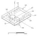
도3 및 도4 는 본 발명의 일 실시예에 따른 도파관과 유전체 도파관의 천이 구조의 사시도와 측면도를 나타낸다.
도5 내지 도8 은 도3 에 도시된 본 발명의 도파관과 유전체 도파관의 천이 구조에서 각 구성 요소를 상세하게 나타낸 도면이다.
도9 는 본 발명의 도파관과 유전체 도파관의 천이 구조에 따른 동작 주파수별 신호 천이 특성에 대한 시뮬레이션 결과를 나타낸다.
도10 은 본 발명의 다른 실시예에 따른 도파관과 유전체 도파관의 천이 구조의 사시도를 나타낸 도면이다.
도11 은 도10 의 천이 구조에 따른 동작 주파수별 신호 천이 특성에 대한 시뮬레이션 결과를 나타낸다. Fig. 1 shows a schematic configuration of a general vehicular radar.
Figure 2 shows the basic structure of a typical dielectric waveguide.
3 and 4 are a perspective view and a side view of a transition structure of a waveguide and a dielectric waveguide according to an embodiment of the present invention.
FIGS. 5 to 8 are diagrams showing the respective components in the transition structure of the waveguide and the dielectric waveguide of the present invention shown in FIG. 3 in detail.
9 shows a simulation result of a signal transition characteristic according to an operating frequency according to a transition structure of a waveguide and a dielectric waveguide of the present invention.
10 is a perspective view illustrating a transition structure of a waveguide and a dielectric waveguide according to another embodiment of the present invention.
FIG. 11 shows a simulation result of signal transition characteristics according to operating frequencies according to the transition structure of FIG.
본 발명과 본 발명의 동작상의 이점 및 본 발명의 실시에 의하여 달성되는 목적을 충분히 이해하기 위해서는 본 발명의 바람직한 실시예를 예시하는 첨부 도면 및 첨부 도면에 기재된 내용을 참조하여야만 한다. In order to fully understand the present invention, operational advantages of the present invention, and objects achieved by the practice of the present invention, reference should be made to the accompanying drawings and the accompanying drawings which illustrate preferred embodiments of the present invention.
이하, 첨부한 도면을 참조하여 본 발명의 바람직한 실시예를 설명함으로써, 본 발명을 상세히 설명한다. 그러나, 본 발명은 여러 가지 상이한 형태로 구현될 수 있으며, 설명하는 실시예에 한정되는 것이 아니다. 그리고, 본 발명을 명확하게 설명하기 위하여 설명과 관계없는 부분은 생략되며, 도면의 동일한 참조부호는 동일한 부재임을 나타낸다. BEST MODE FOR CARRYING OUT THE INVENTION Hereinafter, the present invention will be described in detail with reference to the preferred embodiments of the present invention with reference to the accompanying drawings. However, the present invention can be implemented in various different forms, and is not limited to the embodiments described. In order to clearly describe the present invention, parts that are not related to the description are omitted, and the same reference numerals in the drawings denote the same members.
명세서 전체에서, 어떤 부분이 어떤 구성요소를 "포함"한다고 할 때, 이는 특별히 반대되는 기재가 없는 한 다른 구성요소를 제외하는 것이 아니라, 다른 구성요소를 더 포함할 수 있는 것을 의미한다. 또한, 명세서에 기재된 "...부", "...기", "모듈", "블록" 등의 용어는 적어도 하나의 기능이나 동작을 처리하는 단위를 의미하며, 이는 하드웨어나 소프트웨어 또는 하드웨어 및 소프트웨어의 결합으로 구현될 수 있다. Throughout the specification, when an element is referred to as "including" an element, it does not exclude other elements unless specifically stated to the contrary. The terms "part", "unit", "module", "block", and the like described in the specification mean units for processing at least one function or operation, And a combination of software.
도3 및 도4 는 본 발명의 일 실시예에 따른 도파관과 유전체 도파관의 천이 구조의 사시도와 측면도를 나타낸다.3 and 4 are a perspective view and a side view of a transition structure of a waveguide and a dielectric waveguide according to an embodiment of the present invention.
도3 및 도4 를 참조하여 본 발명에 다른 도파관과 유전체 도파관의 천이 구조에 대해 설명하면, 먼저 유전체 도파관(100)의 하부면에 도파관(200)이 직교하여 직접 결합된다.Referring to FIGS. 3 and 4, the transition structure of the waveguide and the dielectric waveguide according to the present invention will be described. First, the
도파관(200)은 금속관의 형태로 형성되고, 2개의 개구면 중 일면이 유전체 도파관(100)의 하부면에 결합된다. 도파관(200)은 마이크로 파 이상의 고주파수(1GHz)의 신호를 전송하기 위해 금속관 형태로 형성되는 전송로의 일종으로, 단면이 사각형, 원형을 포함한 다양한 형상의 관형태로 구현될 수 있으나, 도3 및 4 에서는 대표적인 일예로 표준 도파관(Standard Waveguide)를 도시하였다. 표준 도파관은 단면이 원형 또는 사각형으로 규정되어 있으며, 단면의 크기는 전송할 신호의 주파수와 차단 주파수에 따라 Electronic Industry Association에 의해 지정되어 있다.The
유전체 도파관(100)은 테프론 등으로 구현되는 유전체 기판(101)과 유전체 기판(101)의 상부면에 배치된 제1 도체(102), 유전체 기판(101)의 하부면에 배치되는 제2 도체(103) 및 상기 유전체 기판(101) 내부에 삽입되어 상기 제1 도체(102)와 제2 도체(103)를 전기적으로 연결하는 복수개의 비아(110)를 구비한다.The
복수개의 비아(110)는 유전체 기판(101)내에서 밀리미터파의 신호가 전송될 전송 선로(TL)를 형성하기 위한 제1 패턴 및 신호를 도파관(200)으로 천이시키기 위한 제2 패턴에 따라 배열된다.The plurality of
제1 패턴은 유전체 기판(101) 내부로 전달되는 신호의 전송 경로에 따라 지정되는 전송 선로(TL)를 형성하기 위해 도2 와 같이 복수개의 비아(110)가 2열로 나란하게 진행하는 형태를 갖는다. 제1 패턴에 의해 형성되는 전송 선로(TL)는 송신 RF 모듈(TRF) 또는 수신 안테나(RANT)에서 인가된 신호를 도파관(200)으로 전달하거나, 도파관(200)을 통해 인가된 신호를 수신 RF 모듈(RRF) 또는 송신 안테나(TANT)로 전달한다.The first pattern has a form in which a plurality of
그리고 제2 패턴은 유전체 도파관(100)과 도파관(200) 사이로 전달되는 신호가 천이되도록, 임피던스 정합기를 형성하는 구성이다. 제2 패턴은 유전체 도파관(100)의 하부면에 결합된 도파관(200)의 결합면 주변으로 기설정된 거리를 두고 복수개의 비아(110)가 배치되는 형태를 갖는다. 다만 제2 패턴은 제1 패턴에 의해 형성된 전송 경로를 통해 인가되는 신호가 도파관(200)으로 전달 될 수 있도록 제1 패턴과 연결되는 위치에 대해서는 비아(110)를 배치하지 않는다. 즉 제2 패턴은 도파관(200)과 결합되는 결합면의 주위에서 제1 패턴에 의해 형성된 전송 경로와 중첩되지 않는 나머지 영역에 상기 결합면으로부터 기설정된 제1 거리만큼 이격되어 복수개의 비아가 배치되는 형태를 갖는다.And the second pattern forms an impedance matcher such that a signal transmitted between the
제1 패턴에 따라 배치되는 복수개의 비아를 제1 비아라하고, 제2 패턴에 따라 배치되는 복수개의 비아를 제2 비아라 할 수 있다.A plurality of vias arranged in accordance with the first pattern may be referred to as a first bit and a plurality of vias arranged in accordance with the second pattern may be referred to as a second bit.
그리고 유전체 도파관(100)의 제2 도체(103)는 도파관(200)과 임피던스 정합을 위해 표준 도파관(200)에서 결합되는 개구면에 대응하는 영역이 식각되어 비공진 슬롯(slot)(120)이 형성된다. 즉 비공진 슬롯(120)은 제2 도체(103)를 표준 도파관(200)의 개구면의 크기에 대응하는 크기로 식각되어 형성된다. 다만 본 발명에서는 제2 도체(103)를 식각하여 비공진 슬롯(120)이 형성되는 영역 중 복수개의 비아(110)의 제1 패턴에 의해 형성되는 전송 선로(TL)와 연결되는 위치에 합입(invagination, 陷入)되는 형태로 제2 도체(103)가 식각되지 않는 영역을 두어 스터브(stub)(121)를 형성한다. 즉 스터브(121)는 제2 도체(103)를 식각하여 비공진 슬롯(120)을 형성하기 전에, 스터브(121)가 형성될 영역을 마스킹하여 식각되지 않도록 함으로써, 형성될 수 있다. 도3 및 도4 에서는 일예로 스터브(121)가 비공진 슬롯(120)에서 직사각형 형태로 함입되는 것으로 도시하였으나, 스터브(121)의 형상은 임피던스 정합 특성에 따른 광대역 효과를 얻기 위해 삼각형, 마름모, 타원형 등 다양하게 설정될 수 있다.The
본 발명에서 스터브(121)는 유전체 도파관(100)과 도파관(200)이 직교하여 연결될 때 발생하는 임피던스의 부정합을 해소하는 역할을 수행한다. 즉 유전체 도파관(100)과 표준 도파관(200) 사이의 임피던스 매칭을 위해 구비된다. 그리고 스터브(121)는 전송 선로(TL)의 중심부에서 비공진 슬롯(120)의 중심 방향으로 함입되는 형태로 형성되며, 스터브(121)의 길이와 폭은 사용하고자 하는 동작 주파수에서 임피던스 정합을 수행할 수 있도록 결정될 수 있다. 여기서 스터브(121)의 함입 형태 및 크기는 단지 동작 주파수에 의해서만 결정되는 것이 아니라, 도파관(200)의 크기나 유전체 기판(101)의 유전율과 두께, 제1 및 제2 도체의 도전성 및 전송 선로(TL)의 폭 등 다양한 사용 환경을 고려하여 결정되어야 하며, 실험을 통해 최적의 스터브(121) 길이 및 폭이 획득될 수 있다.In the present invention, the
본 발명의 도파관과 유전체 도파관의 천이 구조에서는 도파관(200)이 별도의 공동(cavity) 구조를 필요로 하지 않고, 유전체 도파관(100)에 직접 결합됨에 따라 소형화가 용이하다. 또한 구조가 단순하여, 유전체 도파관(100)이 단일 유전체 기판(101)으로 구성되는 경우에도 동작할 수 있고, 일반적인 PCB 공정만을 사용하여 구현 가능하므로, 저비용으로 제조 가능한 장점이 있다.In the transition structure of the waveguide and the dielectric waveguide according to the present invention, the
도5 내지 도8 은 도3 에 도시된 본 발명의 도파관과 유전체 도파관의 천이 구조에서 각 구성 요소를 상세하게 나타낸 도면이다.FIGS. 5 to 8 are diagrams showing the respective components in the transition structure of the waveguide and the dielectric waveguide of the present invention shown in FIG. 3 in detail.
도5 는 도파관(200)을 상세하게 나타낸 도면으로서, 상기한 바와 같이 본 발명에서는 구형의 표준 도파관(200)이 유전체 도파관(100)의 하부면에 직교하여 직접 결합된다. 도파관(200)이 유전체 도파관(100)의 하부면에 직교하여 직접 결합됨으로써, 유전체 도파관(100)으로 인가되어 수평 방향으로 진행하는 밀리리터파의 신호가 수직 방향의 도파관(200)으로 진행하게 되며, 도파관(200)과 유전체 도파관(100) 사이에 부가적인 구성요소가 포함되지 않으므로, 소형의 단순 구조로 결합될 수 있다.5 is a detailed view of the
도6 은 유전체 도파관(100)의 제2 도체(103)를 상세하게 나타낸 도면으로서, 제2 도체(103)는 유전체 도파관(100)에서 최하부에 배치되어 표준 도파관(200)과 직접 결합된다. 그리고 제2 도체(130)에서 도파관(200)의 개구면에 대응하는 영역은 식각되어 비공진 슬롯(120)이 형성되며, 비공진 슬롯(120)이 형성되는 영역 중 전송 선로(TL)와 연결되는 영역에는 전송 선로(TL)가 연장되는 방향으로 제2 도체(130)가 함입되는 형태로 식각되지 않은 스터브(121)이 형성된다. 즉 스터브(121)는 비공진 슬롯(121)을 형성하기 위해 제2 도체(103)를 식각할 때, 스터브(121)에 대응하는 영역을 식각하지 않음으로써 형성될 수 있다.6 is a detailed view of the
도7 은 유전체 도파관(100)의 복수개의 비아(110)를 상세하게 나타낸 도면으로, 도7 에 도시된 바와 같이 복수개의 비아(110)는 유전체 기판(101) 내부에 삽입되어 제1 도체(102)와 제2 도체(103)을 전기적으로 연결하고, 제1 패턴(PT1) 및 제2 패턴(PT2)에 따라 배치된다. 제1 패턴(PT1)에 따라 배치되는 복수개의 제1 비아는 밀리미터파의 신호가 전송될 전송 선로(TL)을 형성하기 위해 복수개의 비아(110)가 나란히 진행하는 2열을 형성하도록 구성된다. 그리고 제2 패턴(PT2)에 따라 배치되는 복수개의 제2 비아는 전송 선로(TL)을 통해 인가된 신호가 도파관(200)으로 천이되도록 임피던스 정합기를 형성하며, 복수개의 제2 비아가 비공진 슬롯(121)의 주위로 기설정된 제1 거리만큼 이격되어 둘러싸는 형태로 구성된다. 여기서 제2 패턴(PT2)에서 제1 패턴(PT1)에 의해 형성된 전송 선로(TL)과 연결되는 위치에는 제2 비아가 배치되지 않는다.7 illustrates a plurality of
그리고 제1 및 제2 패턴(PT1, PT2)에 따라 배치되는 복수개의 비아(110)는 각각 인접한 비아와 기설정된 제2 거리만큼 이격되어 배치된다. 여기서 복수개의 비아(110) 각각이 인접한 비아와 서로 제2 거리만큼 이격되어 배치되는 것은 유전체 도파관(100)이 효율적으로 밀리미터파의 신호를 전송할 수 있도록 하기 위함으로, 스터브(121)와 유사하게 동작 주파수와 유전체 기판(101)의 유전율과 두께, 제1 및 제2 도체의 도전성 및 전송 선로(TL)의 폭 등 다양한 사용 환경을 고려하여 결정되어야 한다. 제2 거리를 계산하는 방법은 공지된 기술이므로 여기서는 상세하게 설명하지 않는다.The plurality of
도8 은 유전체 도파관(100)의 제1 도체(102)를 상세하게 나타낸 도면으로, 제1 도체(102)는 도6 에 도시된 제2 도체(103)와 달리 도파관(200)이 결합되지 않으므로, 비공진 슬롯(120)이나 스터브(121)가 형성되지 않는다. 따라서 도8 에 도시된 바와 같이 유전체 기판(101)의 상부면에 대응하는 형태로 형성된다.8 is a detailed view of the
상기에서는 도파관의 일예로 표준 도파관을 도시하였으나, 본 발명의 도파관 대 유전체 도파관의 천이 구조에서 도파관은 표준 도파관에 한정되지 않고, 다른 형태의 도파관이 사용되어도 무방하다.Although a standard waveguide is shown as an example of a waveguide in the above description, the waveguide in the transition structure of the waveguide to dielectric waveguide of the present invention is not limited to a standard waveguide, and other types of waveguides may be used.
도9 는 본 발명의 도파관과 유전체 도파관의 천이 구조에 따른 동작 주파수별 신호 천이 특성에 대한 시뮬레이션 결과를 나타낸다.9 shows a simulation result of a signal transition characteristic according to an operating frequency according to a transition structure of a waveguide and a dielectric waveguide of the present invention.
도9 에 도시된 바와 같이, 본 발명의 도파관과 유전체 도파관의 천이 구조는 77GHz의 중심 동작 주파수를 기준으로 -15dB의 대역폭이 대략 75GHz ~ 79GHz (4.1492GHz 범위)로 나타난다. 즉 중심 동작 주파수에 대해 사용 가능한 상대 대역폭이 5.4% 수준으로 종래의 기술에 비해 넓으며, 상대 대역폭 내에서 신호 전송 특성이 비교적 평탄한 형태를 갖게 됨에 따라 신호의 왜곡이 적다는 장점을 갖는다. 특히 스터브(121)에 의한 임피던스 매칭이 용이하여 저손실 전송이 가능하다.As shown in FIG. 9, the transition structure of the waveguide and the dielectric waveguide of the present invention shows a bandwidth of about -15 dB from about 75 GHz to 79 GHz (4.1492 GHz range) based on the center operating frequency of 77 GHz. That is, the usable relative bandwidth to the center operating frequency is 5.4%, which is wider than that of the conventional technology, and signal transmission characteristics are relatively flat within the relative bandwidth, so that the signal distortion is less. In particular, impedance matching by the
도10 은 본 발명의 다른 실시예에 따른 도파관과 유전체 도파관의 천이 구조의 사시도를 나타낸 도면이다.10 is a perspective view illustrating a transition structure of a waveguide and a dielectric waveguide according to another embodiment of the present invention.
도10 의 도파관과 유전체 도파관의 천이 구조는 도3 내지 도8 의 도파관과 유전체 도파관의 천이 구조와 비교하여 도파관(400)의 단면 형상이 사각형 형태가 아니다. 즉 표준 도파관으로 구현되지 않는다. 표준 도파관은 전송할 수파수와 차단할 주파수에 대해 도파관의 형태 및 크기가 규정된 도파관으로, 필요로하는 도파관을 용이하게 설계할 수 있다. 그러나 실제 구현에 있어서는 정확한 형태의 표준 도파관을 구현하기 어렵고, 고비용이 소요된다는 문제가 있다. 따라서 통상적으로 표준 도파관의 형태를 일부 수정한 형태의 도파관이 주로 사용된다. 그리고 도10 에서는 실질적으로 주로 사용되는 도파관 천이 구조를 나타내기 위해 모서리가 직각을 형성하는 사각형 형태의 표준 도파관이 아닌 모서리가 둥근 형태의 도파관(400)을 일예로 사용하였다.10, the cross-sectional shape of the waveguide 400 is not rectangular compared to that of the waveguide and dielectric waveguide of FIGS. It is not implemented as a standard waveguide. A standard waveguide is a waveguide in which the shape and size of the waveguide are specified for the waveguide to be transmitted and the frequency to be cut off, so that the required waveguide can be easily designed. However, in actual implementation, it is difficult to implement a standard waveguide of the correct type, and there is a problem that a high cost is required. Therefore, a waveguide in which a shape of a standard waveguide is partially modified is usually used. In FIG. 10, a waveguide 400 having a rounded corner shape is used instead of a standard waveguide having a rectangular shape in which corners are formed at right angles in order to represent a waveguide transition structure that is mainly used.
그리고 스터브(321) 형상 또한 도3 내지 도8 과 달리 직사각형이 아닌 삼각형과 유사한 형태로 구현되었다. 도10 에서 스터브(321)는 삼각형의 모서리가 모내기되어 윗변의 길이가 매우 짧은 사다리꼴 형태로 구현될 수 있으며, 모서리가 라운드된 형태로 구현될 수도 있다. 도10 의 스터브(321) 형상은 상기한 바와 같이, 임피던스 정합 특성에 따른 광대역 효과를 얻기 위한 것으로, 스터브(321)의 형상은 다양하게 변화될 수 있다.Also, the shape of the
도11 은 도10 의 천이 구조에 따른 동작 주파수별 신호 천이 특성에 대한 시뮬레이션 결과를 나타낸다. FIG. 11 shows a simulation result of signal transition characteristics according to operating frequencies according to the transition structure of FIG.
도 11 의 시뮬레이션 결과를 도9 의 시뮬레이션 결과와 비교하면, 스터브의 형상이 변형됨에 따라, 중심 동작 주파수를 기준으로 -15dB의 대역폭이 대략 73GHz ~ 80GHz (6.4637GHz 범위)로 나타난다. 즉 임피던스 정합 특성이 변화되어 광대역 효과를 얻을 수 있다. 또한 상대 대역폭 내에서 신호 전송 특성이 비교적 평탄한 형태를 갖게 됨에 따라 신호의 왜곡이 적고, 저손실 전송이 가능하다.Comparing the simulation result of FIG. 11 with the simulation result of FIG. 9, as the shape of the stub is changed, a bandwidth of -15 dB based on the center operating frequency appears in the range of approximately 73 GHz to 80 GHz (6.4637 GHz range). That is, the impedance matching characteristic is changed, and a broadband effect can be obtained. Also, signal transmission characteristics are relatively flat within the relative bandwidth, so that signal distortion is small and low loss transmission is possible.
본 발명에 따른 방법은 컴퓨터로 읽을 수 있는 기록매체에 컴퓨터가 읽을 수 있는 코드로서 구현하는 것이 가능하다. 컴퓨터가 읽을 수 있는 기록매체는 컴퓨터 시스템에 의하여 읽혀질 수 있는 데이터가 저장되는 모든 종류의 기록장치를 포함한다. 기록매체의 예로는 ROM, RAM, CD-ROM, 자기 테이프, 플로피 디스크, 광데이터 저장장치 등이 있으며, 또한 캐리어 웨이브(예를 들어 인터넷을 통한 전송)의 형태로 구현되는 것도 포함한다. 또한 컴퓨터가 읽을 수 있는 기록매체는 네트워크로 연결된 컴퓨터 시스템에 분산되어 분산방식으로 컴퓨터가 읽을 수 있는 코드가 저장되고 실행될 수 있다.The method according to the present invention can be implemented as a computer-readable code on a computer-readable recording medium. A computer-readable recording medium includes all kinds of recording apparatuses in which data that can be read by a computer system is stored. Examples of the recording medium include a ROM, a RAM, a CD-ROM, a magnetic tape, a floppy disk, an optical data storage device, and the like, and a carrier wave (for example, transmission via the Internet). The computer-readable recording medium may also be distributed over a networked computer system so that computer readable code can be stored and executed in a distributed manner.
본 발명은 도면에 도시된 실시예를 참고로 설명되었으나 이는 예시적인 것에 불과하며, 본 기술 분야의 통상의 지식을 가진 자라면 이로부터 다양한 변형 및 균등한 타 실시예가 가능하다는 점을 이해할 것이다. While the present invention has been particularly shown and described with reference to exemplary embodiments thereof, it is evident that many alternatives, modifications and variations will be apparent to those skilled in the art.
따라서, 본 발명의 진정한 기술적 보호 범위는 첨부된 등록청구범위의 기술적 사상에 의해 정해져야 할 것이다.Accordingly, the true scope of the present invention should be determined by the technical idea of the appended claims.
Claims (10)
금속관으로 형성되어 상기 유전체 도파관의 하부면에 직교 방향으로 직접 결합되는 도파관; 을 포함하고,
상기 유전체 도파관은
유전체 기판;
상기 유전체 기판의 상부면에 배치되는 제1 도체;
상기 유전체 기판의 하부면에 배치되고, 상기 도파관의 개구면에 대응하는 영역이 식각되어 비공진 슬롯이 형성되는 제2 도체;
기설정된 패턴에 따라 상기 유전체 기판 내에 배치되어, 상기 유전체 도파관 내에서 신호가 전송되는 경로인 전송 선로와 상기 유전체 도파관 또는 상기 도파관으로 전송되는 신호를 천이시키기 위한 임피던스 정합기를 형성하는 복수개의 비아; 및
상기 비공진 슬롯이 형성되는 영역 내에서 중심축이 상기 비공진 슬롯과 연결되는 전송 선로의 중심축에서 상기 비공진 슬롯의 중심 방향을 따라 함입되는 형태로 형성되어, 상기 유전체 도파관과 상기 도파관 사이의 임피던스 매칭을 수행하는 하나의 스터브; 를 구비하는 것을 특징으로 하는 도파관 대 유전체 도파관의 천이 구조.Dielectric waveguide; And
A waveguide formed of a metal tube and directly coupled to the lower surface of the dielectric waveguide in an orthogonal direction; / RTI >
The dielectric waveguide
A dielectric substrate;
A first conductor disposed on an upper surface of the dielectric substrate;
A second conductor disposed on a lower surface of the dielectric substrate and having an area corresponding to an opening surface of the waveguide being etched to form a non-resonant slot;
A plurality of vias formed in the dielectric substrate according to a predetermined pattern to form an impedance matching device for transiting a transmission line that is a path through which signals are transmitted in the dielectric waveguide and a signal transmitted to the dielectric waveguide or the waveguide; And
Resonant slot is formed in a central axis of the transmission line connected to the non-resonant slot along a center direction of the non-resonant slot, and the center axis of the dielectric waveguide One stub for performing impedance matching; And a waveguide-to-dielectric waveguide.
상기 신호가 상기 유전체 기판 내에서 기설정된 경로에 따라 전송되도록 상기 경로의 양측을 가이드하는 제1 패턴에 따라 배치되어 상기 전송 선로를 형성하는 복수개의 제1 비아; 및
상기 비공진 슬롯의 외곽으로 기설정된 제1 거리만큼 이격되는 제2 패턴에 따라 배치되어 상기 임피던스 정합기를 형성하는 복수개의 제2 비아: 를 포함하는 것을 특징으로 하는 도파관 대 유전체 도파관의 천이 구조.2. The method of claim 1, wherein the plurality of vias
A plurality of first vias disposed along a first pattern guiding both sides of the path such that the signals are transmitted along a predetermined path in the dielectric substrate to form the transmission line; And
And a plurality of second vias arranged according to a second pattern spaced apart by a predetermined first distance from the outer periphery of the non-resonant slot to form the impedance matcher.
상기 비공진 슬롯과 상기 전송 선로가 연결되는 위치에는 상기 제2 비아가 배치되지 않도록 설정되는 것을 특징으로 하는 도파관 대 유전체 도파관의 천이 구조.3. The method of claim 2, wherein the second pattern
And wherein the second via is not disposed at a position where the non-resonant slot and the transmission line are connected to each other.
상기 비공진 슬롯이 형성될 때, 상기 제2 도체에서 상기 스터브에 대응하는 영역이 식각되지 않도록 마스킹되어 형성되는 것을 특징으로 하는 도파관 대 유전체 도파관의 천이 구조.4. The apparatus of claim 3, wherein the stub
Wherein the second conductor is masked so that the region corresponding to the stub is not etched when the non-resonant slot is formed.
형태 및 크기가 상기 신호의 주파수와 상기 도파관의 크기, 상기 유전체 기판의 유전율과 두께 및 상기 제1 및 제2 도체의 도전성 및 상기 전송 선로의 폭 중 적어도 하나에 따라 다르게 설정되는 것을 특징으로 하는 도파관 대 유전체 도파관의 천이 구조.6. The apparatus of claim 5, wherein the stub
The shape and size of which are set differently depending on at least one of the frequency of the signal and the size of the waveguide, the dielectric constant and thickness of the dielectric substrate, the conductivity of the first and second conductors, and the width of the transmission line. Transition structure of large dielectric waveguide.
직사각형 형태로 형성되는 것을 특징으로 하는 도파관 대 유전체 도파관의 천이 구조.7. The apparatus of claim 6, wherein the stub
Wherein the waveguide-to-dielectric waveguide is formed in a rectangular shape.
사다리꼴 형태로 형성되는 것을 특징으로 하는 도파관 대 유전체 도파관의 천이 구조.7. The apparatus of claim 6, wherein the stub
Wherein the waveguide-to-dielectric waveguide is formed in a trapezoidal shape.
70 ~ 110 GHz 대역의 밀리미터파의 신호인 것을 특징으로 하는 도파관 대 유전체 도파관의 천이 구조.The method of claim 1,
Wherein the waveguide-to-dielectric waveguide is a millimeter-wave signal in the 70 to 110 GHz band.
각각 인접한 비아와 기설정된 제2 거리만큼 이격되어 배치되는 것을 특징으로 하는 도파관 대 유전체 도파관의 천이 구조.2. The method of claim 1, wherein the plurality of vias
Wherein the first and second waveguides are disposed apart from each other by a predetermined second distance.
Priority Applications (3)
| Application Number | Priority Date | Filing Date | Title |
|---|---|---|---|
| KR1020140139905A KR101621480B1 (en) | 2014-10-16 | 2014-10-16 | Transit structure of waveguide and dielectric waveguide |
| CN201410674764.9A CN105680135A (en) | 2014-10-16 | 2014-11-21 | Transit structure of waveguide and dielectric waveguide |
| US14/592,705 US9450281B2 (en) | 2014-10-16 | 2015-01-08 | Transit structure of waveguide and SIW |
Applications Claiming Priority (1)
| Application Number | Priority Date | Filing Date | Title |
|---|---|---|---|
| KR1020140139905A KR101621480B1 (en) | 2014-10-16 | 2014-10-16 | Transit structure of waveguide and dielectric waveguide |
Publications (2)
| Publication Number | Publication Date |
|---|---|
| KR20160044873A KR20160044873A (en) | 2016-04-26 |
| KR101621480B1 true KR101621480B1 (en) | 2016-05-16 |
Family
ID=55749783
Family Applications (1)
| Application Number | Title | Priority Date | Filing Date |
|---|---|---|---|
| KR1020140139905A Active KR101621480B1 (en) | 2014-10-16 | 2014-10-16 | Transit structure of waveguide and dielectric waveguide |
Country Status (3)
| Country | Link |
|---|---|
| US (1) | US9450281B2 (en) |
| KR (1) | KR101621480B1 (en) |
| CN (1) | CN105680135A (en) |
Cited By (1)
| Publication number | Priority date | Publication date | Assignee | Title |
|---|---|---|---|---|
| CN110336106A (en) * | 2019-07-19 | 2019-10-15 | 成都频岢微电子有限公司 | A kind of miniaturized substrate integrated waveguide filter and its higher order filter |
Families Citing this family (39)
| Publication number | Priority date | Publication date | Assignee | Title |
|---|---|---|---|---|
| CN108604722B (en) * | 2016-02-12 | 2021-04-16 | 瑞典爱立信有限公司 | Transition device including non-contact transition or connection between SIW and waveguide or antenna |
| EP3240101B1 (en) * | 2016-04-26 | 2020-07-29 | Huawei Technologies Co., Ltd. | Radiofrequency interconnection between a printed circuit board and a waveguide |
| US10199707B2 (en) | 2016-10-13 | 2019-02-05 | Aptiv Technologies Limited | Ball-grid-array radio-frequency integrated-circuit printed-circuit-board assembly for automated vehicles |
| US10468736B2 (en) * | 2017-02-08 | 2019-11-05 | Aptiv Technologies Limited | Radar assembly with ultra wide band waveguide to substrate integrated waveguide transition |
| CN106997981A (en) * | 2017-03-13 | 2017-08-01 | 电子科技大学 | A kind of vertical transition device of Ka band rectangular waveguides to substrate integration wave-guide |
| KR101974370B1 (en) * | 2017-11-08 | 2019-05-02 | 한국철도기술연구원 | Microstripe-waveguide transition device |
| US11139581B2 (en) * | 2019-03-07 | 2021-10-05 | Aptiv Technologies Limited | Signaling device including a slot transition between a substrate integrated waveguide and a signal generator |
| US11527808B2 (en) | 2019-04-29 | 2022-12-13 | Aptiv Technologies Limited | Waveguide launcher |
| CN110071352B (en) * | 2019-04-29 | 2020-12-25 | 中国科学技术大学 | Full magnetic wall triangle filter |
| DE102020119495A1 (en) | 2020-07-23 | 2022-01-27 | Fraunhofer-Gesellschaft zur Förderung der angewandten Forschung eingetragener Verein | High-frequency structure with substrate-integrated waveguide and rectangular waveguide |
| US11362436B2 (en) | 2020-10-02 | 2022-06-14 | Aptiv Technologies Limited | Plastic air-waveguide antenna with conductive particles |
| US11757166B2 (en) | 2020-11-10 | 2023-09-12 | Aptiv Technologies Limited | Surface-mount waveguide for vertical transitions of a printed circuit board |
| KR102220423B1 (en) * | 2020-11-10 | 2021-02-25 | 코모텍 주식회사 | Waveguide antenna with single layer feed network structure using dielectric substance |
| US11749883B2 (en) | 2020-12-18 | 2023-09-05 | Aptiv Technologies Limited | Waveguide with radiation slots and parasitic elements for asymmetrical coverage |
| US11681015B2 (en) | 2020-12-18 | 2023-06-20 | Aptiv Technologies Limited | Waveguide with squint alteration |
| US11502420B2 (en) | 2020-12-18 | 2022-11-15 | Aptiv Technologies Limited | Twin line fed dipole array antenna |
| US11626668B2 (en) | 2020-12-18 | 2023-04-11 | Aptiv Technologies Limited | Waveguide end array antenna to reduce grating lobes and cross-polarization |
| US11901601B2 (en) | 2020-12-18 | 2024-02-13 | Aptiv Technologies Limited | Waveguide with a zigzag for suppressing grating lobes |
| US11444364B2 (en) | 2020-12-22 | 2022-09-13 | Aptiv Technologies Limited | Folded waveguide for antenna |
| US11668787B2 (en) | 2021-01-29 | 2023-06-06 | Aptiv Technologies Limited | Waveguide with lobe suppression |
| US12058804B2 (en) | 2021-02-09 | 2024-08-06 | Aptiv Technologies AG | Formed waveguide antennas of a radar assembly |
| US11721905B2 (en) | 2021-03-16 | 2023-08-08 | Aptiv Technologies Limited | Waveguide with a beam-forming feature with radiation slots |
| US11616306B2 (en) | 2021-03-22 | 2023-03-28 | Aptiv Technologies Limited | Apparatus, method and system comprising an air waveguide antenna having a single layer material with air channels therein which is interfaced with a circuit board |
| EP4084222A1 (en) | 2021-04-30 | 2022-11-02 | Aptiv Technologies Limited | Dielectric loaded waveguide for low loss signal distributions and small form factor antennas |
| US11973268B2 (en) | 2021-05-03 | 2024-04-30 | Aptiv Technologies AG | Multi-layered air waveguide antenna with layer-to-layer connections |
| US11962085B2 (en) | 2021-05-13 | 2024-04-16 | Aptiv Technologies AG | Two-part folded waveguide having a sinusoidal shape channel including horn shape radiating slots formed therein which are spaced apart by one-half wavelength |
| US11616282B2 (en) | 2021-08-03 | 2023-03-28 | Aptiv Technologies Limited | Transition between a single-ended port and differential ports having stubs that match with input impedances of the single-ended and differential ports |
| US12224502B2 (en) | 2021-10-14 | 2025-02-11 | Aptiv Technologies AG | Antenna-to-printed circuit board transition |
| CN114256579B (en) * | 2021-12-24 | 2022-07-29 | 电子科技大学 | A D-band SIW Leroy coupling structure and its design method |
| US12456816B2 (en) | 2022-05-02 | 2025-10-28 | Aptiv Technologies AG | Waveguide with slot antennas and reflectors |
| US12265172B2 (en) | 2022-05-25 | 2025-04-01 | Aptiv Technologies AG | Vertical microstrip-to-waveguide transition |
| US12315999B2 (en) | 2022-07-15 | 2025-05-27 | Aptiv Technologies AG | Solderable waveguide antenna |
| CN115603015A (en) * | 2022-11-10 | 2023-01-13 | 上海无线电设备研究所(Cn) | A Wide Stop Band Substrate Integrated Waveguide Filter |
| US12424767B2 (en) | 2022-11-15 | 2025-09-23 | Aptiv Technologies AG | Planar surface features for waveguide and antenna |
| US12537308B2 (en) | 2023-01-24 | 2026-01-27 | Aptiv Technologies AG | Symmetrical two-piece waveguide |
| US12148992B2 (en) | 2023-01-25 | 2024-11-19 | Aptiv Technologies AG | Hybrid horn waveguide antenna |
| US12506272B2 (en) | 2023-05-16 | 2025-12-23 | Aptiv Technologies AG | Production-tolerant multi-part antenna system |
| CN116706480B (en) * | 2023-07-21 | 2024-06-21 | 南京邮电大学 | A compact, highly selective substrate-integrated waveguide triangular cavity wide stopband filter |
| KR102824817B1 (en) * | 2023-12-27 | 2025-06-25 | 한국전자기술연구원 | Method for impedance matching of waveguide and SIW transmission line, and SIW transmission line adopting the method |
Citations (4)
| Publication number | Priority date | Publication date | Assignee | Title |
|---|---|---|---|---|
| JP2004153415A (en) | 2002-10-29 | 2004-05-27 | Kyocera Corp | High frequency line-waveguide converter |
| JP2005020415A (en) | 2003-06-26 | 2005-01-20 | Kyocera Corp | Connection structure between dielectric waveguide line and waveguide, and antenna device and filter device using the structure |
| JP2011061258A (en) * | 2009-09-05 | 2011-03-24 | Fujitsu Ltd | Signal converter, and method for manufacturing the same |
| JP2012199659A (en) | 2011-03-18 | 2012-10-18 | Toshiba Corp | Waveguide connection structure, antenna device and radar device |
Family Cites Families (12)
| Publication number | Priority date | Publication date | Assignee | Title |
|---|---|---|---|---|
| US6127901A (en) | 1999-05-27 | 2000-10-03 | Hrl Laboratories, Llc | Method and apparatus for coupling a microstrip transmission line to a waveguide transmission line for microwave or millimeter-wave frequency range transmission |
| JP2003078310A (en) * | 2001-09-04 | 2003-03-14 | Murata Mfg Co Ltd | High-frequency line converter, component, module and communication device |
| JP3828438B2 (en) * | 2002-03-13 | 2006-10-04 | 三菱電機株式会社 | Waveguide / microstrip line converter |
| JP4058381B2 (en) * | 2003-05-29 | 2008-03-05 | 京セラ株式会社 | Connection structure between dielectric waveguide line and waveguide, and antenna substrate and filter substrate using the structure |
| KR100576552B1 (en) | 2004-12-16 | 2006-05-03 | 한국전자통신연구원 | Transition Structure of Dielectric Waveguide and Millimeter Waveguide in Millimeter Wave Band |
| KR100714451B1 (en) | 2005-12-08 | 2007-05-04 | 한국전자통신연구원 | Dielectric Waveguide vs. Standard Waveguide Transition |
| JP4568235B2 (en) * | 2006-02-08 | 2010-10-27 | 株式会社デンソー | Transmission line converter |
| JP4453696B2 (en) | 2006-11-22 | 2010-04-21 | 株式会社村田製作所 | Waveguide-high frequency line converter and wireless communication device |
| EP2110884B1 (en) | 2008-04-15 | 2013-05-29 | Sub10 Systems Limited | Surface-mountable antenna with waveguide connector function, communication system, adaptor and arrangement comprising the antenna device |
| JP2010114826A (en) * | 2008-11-10 | 2010-05-20 | Mitsubishi Electric Corp | Method of manufacturing waveguide slot antenna substrate |
| CN201383535Y (en) * | 2009-04-01 | 2010-01-13 | 惠州市硕贝德通讯科技有限公司 | Rectangular waveguide-substrate integrated waveguide signal conversion and power divider |
| CN102509833B (en) * | 2011-10-26 | 2013-09-25 | 电子科技大学 | Device for converting substrate integrated waveguide to coaxial waveguide |
-
2014
- 2014-10-16 KR KR1020140139905A patent/KR101621480B1/en active Active
- 2014-11-21 CN CN201410674764.9A patent/CN105680135A/en active Pending
-
2015
- 2015-01-08 US US14/592,705 patent/US9450281B2/en active Active
Patent Citations (4)
| Publication number | Priority date | Publication date | Assignee | Title |
|---|---|---|---|---|
| JP2004153415A (en) | 2002-10-29 | 2004-05-27 | Kyocera Corp | High frequency line-waveguide converter |
| JP2005020415A (en) | 2003-06-26 | 2005-01-20 | Kyocera Corp | Connection structure between dielectric waveguide line and waveguide, and antenna device and filter device using the structure |
| JP2011061258A (en) * | 2009-09-05 | 2011-03-24 | Fujitsu Ltd | Signal converter, and method for manufacturing the same |
| JP2012199659A (en) | 2011-03-18 | 2012-10-18 | Toshiba Corp | Waveguide connection structure, antenna device and radar device |
Cited By (1)
| Publication number | Priority date | Publication date | Assignee | Title |
|---|---|---|---|---|
| CN110336106A (en) * | 2019-07-19 | 2019-10-15 | 成都频岢微电子有限公司 | A kind of miniaturized substrate integrated waveguide filter and its higher order filter |
Also Published As
| Publication number | Publication date |
|---|---|
| US20160111764A1 (en) | 2016-04-21 |
| US9450281B2 (en) | 2016-09-20 |
| KR20160044873A (en) | 2016-04-26 |
| CN105680135A (en) | 2016-06-15 |
Similar Documents
| Publication | Publication Date | Title |
|---|---|---|
| KR101621480B1 (en) | Transit structure of waveguide and dielectric waveguide | |
| US6954177B2 (en) | Microstrip antenna array with periodic filters for enhanced performance | |
| KR101518429B1 (en) | Antenna array for ultra wide band radar applications | |
| JP3163981B2 (en) | Transceiver | |
| JP3287309B2 (en) | Directional coupler, antenna device, and transmission / reception device | |
| US11223112B2 (en) | Inverted microstrip travelling wave patch array antenna system | |
| US11515624B2 (en) | Integrated cavity backed slot array antenna system | |
| EP2533362B1 (en) | Microstrip antenna and radar module | |
| CN114649660B (en) | Waveguide with skew change | |
| US9817105B2 (en) | Stacked waveguide substrate, radio communication module, and radar system | |
| CA3096346C (en) | Array antenna apparatus and communication device | |
| CN113381169B (en) | Antenna and radar system | |
| CN110311211B (en) | A microstrip receiving antenna, a transmitting antenna and a vehicle-mounted phased array antenna | |
| CN220934397U (en) | Wide-beam millimeter wave antenna and radar equipment | |
| CN115411480A (en) | Radio frequency structure, detection device and communication system | |
| CN210516980U (en) | Microstrip receiving antenna, transmitting antenna and vehicle-mounted phased array antenna | |
| CN115015898B (en) | Radar device for detecting target objects | |
| US11967765B1 (en) | Low side lobe level integrated cavity backed slot array antenna system | |
| Han et al. | Miniaturization of SIW-based linearly polarized slot antennas for software-defined radar | |
| WO2024168590A1 (en) | Waveguide apparatus and related product | |
| CN113571892A (en) | An antenna device, a vehicle-mounted millimeter-wave radar, and a vehicle |
Legal Events
| Date | Code | Title | Description |
|---|---|---|---|
| A201 | Request for examination | ||
| PA0109 | Patent application |
Patent event code: PA01091R01D Comment text: Patent Application Patent event date: 20141016 |
|
| PA0201 | Request for examination | ||
| E902 | Notification of reason for refusal | ||
| PE0902 | Notice of grounds for rejection |
Comment text: Notification of reason for refusal Patent event date: 20151118 Patent event code: PE09021S01D |
|
| PG1501 | Laying open of application | ||
| E701 | Decision to grant or registration of patent right | ||
| PE0701 | Decision of registration |
Patent event code: PE07011S01D Comment text: Decision to Grant Registration Patent event date: 20160502 |
|
| GRNT | Written decision to grant | ||
| PR0701 | Registration of establishment |
Comment text: Registration of Establishment Patent event date: 20160510 Patent event code: PR07011E01D |
|
| PR1002 | Payment of registration fee |
Payment date: 20160510 End annual number: 3 Start annual number: 1 |
|
| PG1601 | Publication of registration | ||
| FPAY | Annual fee payment |
Payment date: 20190425 Year of fee payment: 4 |
|
| PR1001 | Payment of annual fee |
Payment date: 20190425 Start annual number: 4 End annual number: 4 |
|
| PR1001 | Payment of annual fee |
Payment date: 20200414 Start annual number: 5 End annual number: 5 |
|
| PR1001 | Payment of annual fee |
Payment date: 20210426 Start annual number: 6 End annual number: 6 |
|
| PR1001 | Payment of annual fee |
Payment date: 20220426 Start annual number: 7 End annual number: 7 |
|
| PR1001 | Payment of annual fee |
Payment date: 20230424 Start annual number: 8 End annual number: 8 |