KR101606452B1 - Semiconductor memory device having multi-chip package for implementing other termination and termination control method thereof - Google Patents
Semiconductor memory device having multi-chip package for implementing other termination and termination control method thereof Download PDFInfo
- Publication number
- KR101606452B1 KR101606452B1 KR1020090021240A KR20090021240A KR101606452B1 KR 101606452 B1 KR101606452 B1 KR 101606452B1 KR 1020090021240 A KR1020090021240 A KR 1020090021240A KR 20090021240 A KR20090021240 A KR 20090021240A KR 101606452 B1 KR101606452 B1 KR 101606452B1
- Authority
- KR
- South Korea
- Prior art keywords
- chip
- memory
- termination
- chip enable
- accessed
- Prior art date
- Legal status (The legal status is an assumption and is not a legal conclusion. Google has not performed a legal analysis and makes no representation as to the accuracy of the status listed.)
- Active
Links
Images

Classifications
-
- G—PHYSICS
- G11—INFORMATION STORAGE
- G11C—STATIC STORES
- G11C5/00—Details of stores covered by group G11C11/00
- G11C5/06—Arrangements for interconnecting storage elements electrically, e.g. by wiring
- G11C5/063—Voltage and signal distribution in integrated semi-conductor memory access lines, e.g. word-line, bit-line, cross-over resistance, propagation delay
-
- H10W42/00—
-
- G—PHYSICS
- G11—INFORMATION STORAGE
- G11C—STATIC STORES
- G11C7/00—Arrangements for writing information into, or reading information out from, a digital store
- G11C7/10—Input/output [I/O] data interface arrangements, e.g. I/O data control circuits, I/O data buffers
-
- G—PHYSICS
- G11—INFORMATION STORAGE
- G11C—STATIC STORES
- G11C7/00—Arrangements for writing information into, or reading information out from, a digital store
- G11C7/10—Input/output [I/O] data interface arrangements, e.g. I/O data control circuits, I/O data buffers
- G11C7/1051—Data output circuits, e.g. read-out amplifiers, data output buffers, data output registers, data output level conversion circuits
- G11C7/1057—Data output buffers, e.g. comprising level conversion circuits, circuits for adapting load
Landscapes
- Dram (AREA)
Abstract
본 발명은 아더 터미네이션을 구현하는 멀티 칩 패키지 구조의 반도체 메모리 장치 및 터미네이션 제어 방법에 대하여 개시된다. 반도체 메모리 장치는, 데이터 입출력 라인을 공유하는 적어도 2개 이상의 메모리 칩들을 장착하는 멀티 칩 패키지 구조로 이루어진다. 메모리 칩들 각각은, 자신의 메모리 칩이 억세스되었는지 여부를 판단하는 제1 칩 인에이블 포트, 다른 메모리 칩이 억세스되었는지 여부를 모니터링하는 제2 칩 인에이블 포트, 그리고 제1 또는 제2 칩 인에이블 포트들의 활성화에 응답하여 자신의 메모리 칩 내 터미네이션 저항을 오프시키는 액티브 터미네이션을 포함한다. 메모리 칩들 중 나머지 메모리 칩은 자신의 메모리 칩이 억세스되었는지 여부를 나타내는 칩 인에이블 신호를 수신하는 칩 인에이블 포트를 포함한다.
아더 터미네이션, 제1 및 제2 칩 인에이블 포트들, 액티브 터미네이션
The present invention discloses a semiconductor memory device and a termination control method in a multi-chip package structure that implements Arther termination. The semiconductor memory device comprises a multichip package structure in which at least two memory chips sharing a data input / output line are mounted. Each of the memory chips includes a first chip enable port for determining whether its memory chip is accessed, a second chip enable port for monitoring whether another memory chip has been accessed, and a second chip enable port, Lt; RTI ID = 0.0 > termination < / RTI > The remaining memory chips of the memory chips include a chip enable port that receives a chip enable signal indicating whether or not its memory chip is accessed.
Arther termination, first and second chip enable ports, active termination
Description
본 발명은 반도체 메모리 장치에 관한 것으로, 특히 아더 터미네이션을 구현하는 멀티 칩 패키지 구조의 반도체 메모리 장치 및 터미네이션 제어 방법에 관한 것이다.BACKGROUND OF THE INVENTION 1. Field of the Invention The present invention relates to a semiconductor memory device, and more particularly, to a semiconductor memory device and a termination control method in a multichip package structure that implements Arther termination.
다수의 전자 시스템은 서로 간에 정보를 주고받는 컨트롤러와 메모리 장치를 채용한다. 통상적으로, 정보는 하나 이상의 시스템 버스를 통하여 송수신된다. 이들 버스들은 전송 라인으로서 작용한다. 이에 따라, 이들 버스 라인들은 전송 라인에 결합되는 장치와 연관된 신호 반사를 고려한 설계를 요구한다. 전송 라인은, 전송 라인과 전원 노드 사이에 연결된 저항을 이용하여 터미네이션된다.Many electronic systems employ controllers and memory devices that exchange information with each other. Typically, information is transmitted and received via one or more system buses. These buses act as transmission lines. These bus lines thus require a design that takes into account the signal reflections associated with the devices coupled to the transmission lines. The transmission line is terminated using a resistor connected between the transmission line and the power supply node.
컴퓨터와 같은 외부 시스템에 대해, 컴퓨터의 마더 보드 상에 종종 배치되는 외부 저항들에 의해 터미네이션이 제공된다. 전송 라인의 임피던스와 매칭되는 임피던스를 가지는 외부 저항이 선택되어, 다수의 집적 회로들과 접속하는 상호 접속 신호 라인과 같은 전송 라인을 터미네이션한다. 외부 저항이 전송 라인 임피던스와 매칭될 때, 신호 반사가 거의 없거나 전혀 없다. 그러나, 시스템 보드 상에 배치되는 모든 전송 라인에 대한 외부 저항은 이들 보드 상에서 큰 면적을 차지한다.For external systems such as computers, termination is provided by external resistors, which are often placed on the motherboard of the computer. An external resistor having an impedance matching the impedance of the transmission line is selected to terminate the transmission line, such as an interconnection signal line, connecting to a plurality of integrated circuits. When the external resistance is matched with the transmission line impedance, there is little or no signal reflection. However, the external resistance for all transmission lines disposed on the system board occupies a large area on these boards.
외부 저항의 대안으로서, 액티브 터미네이션으로 알려진 온 칩 터미네이션 또는 온 다이 터미네이션이 시스템의 집적 회로에 이용된다. 액티브 터미네이션은, 예컨대, 메모리 장치와 콘트롤러 칩 셋 내부에 각각 터미네이션 저항을 삽입하고, 삽입된 저항을 필요에 따라서 온/오프시키는 방식을 말한다. 터미네이션 저항을 온/오프시키는 방법은, 메모리 장치의 구성(configuration)과 입력되는 커맨드에 따라 변경될 수 있다. 메모리 장치의 구성에 의한 터미네이션 변경은 모드 레지스터 셋팅과 같은 방법을 이용하여 콘트롤러로부터 제어될 수 있다. 커맨드에 의한 터미네이션 온/오프 방법은 현재 입력되는 커맨드가 자신의 메모리 장치로 발행(issue)된 것인지 여부를 판단하여 이루어진다.As an alternative to external resistors, on-chip termination or on-die termination, known as active termination, is used in the integrated circuit of the system. The active termination refers to a method of inserting termination resistors in the memory device and the controller chip set, respectively, and turning on and off the inserted resistors as necessary. The method of turning on / off the termination resistance can be changed according to the configuration of the memory device and the command to be inputted. The termination change by the configuration of the memory device can be controlled from the controller using the same method as the mode register setting. The termination on / off method by the command is performed by judging whether or not the currently input command is issued to the own memory device.
한편, 메모리 장치가 데이터 라인을 공유하는 적어도 2 이상의 메모리 칩을 장착하는 멀티 칩 패키지(Multi-Chip Package: MCP) 구조로 이루어진 경우, 각각의 메모리 칩은 해당 메모리 칩의 칩 인에이블(Chip Enable: CE) 신호의 활성화에 따라 자신의 메모리 칩 내 터미네이션 저항을 온 시킬 수 있다. 이를 "셀프 터미네이션(self termination)" 이라 한다. 셀프 터미네이션과 반대되는 개념으로, 해당 메모리 칩의 칩 인에이블(Chip Enable: CE) 신호의 활성화에 따라 자신 이외의 다른 메모리 칩 내 터미네이션 저항을 온 시킬 수 있는 데, 이를 "아더 터미네이션(other termination)"이라 한다.Meanwhile, when the memory device has a multi-chip package (MCP) structure in which at least two memory chips sharing a data line are mounted, each memory chip has a chip enable CE) signal to activate the termination resistor in its memory chip. This is called "self termination ". Termination resistance in memory chips other than itself can be turned on by activating a chip enable (CE) signal of the memory chip, which is an opposite concept to the self termination. This is called "other termination" "
그런데, MCP 구조의 메모리 장치에 아더 터미네이션을 구현하는 경우, 예컨 대, 제1 메모리 칩과 제2 메모리 칩이 장착된 상태에서 제2 메모리 칩의 칩 인에입블(CE) 신호가 활성화되어 억세스되면, 제1 메모리 칩은 자신의 칩 인에이블(CE) 신호가 활성화되지 않았기 때문에 자신의 터미네이션 저항을 온 시키게 된다. 제1 메모리 칩 내 터미네이션 저항이 온되면, 제1 메모리 칩과 제2 메모리 칩이 데이터 입출력 라인을 공유하고 있기 때문에, 억세스된 제2 메모리 칩의 입장에서는 자신의 데이터 입출력 라인이 터미네이션되는 것과 같은, 즉 셀프 터미네이션되는 문제점이 발생한다.However, when the arithmetic termination is implemented in the memory device of the MCP structure, for example, when a CE signal, which is a chip of the second memory chip, is activated while the first memory chip and the second memory chip are mounted , The first memory chip turns on its termination resistance because its chip enable (CE) signal is not activated. When the termination resistance in the first memory chip is turned on, since the first memory chip and the second memory chip share a data input / output line, the data input / output line of the second memory chip is terminated, That is, a self-termination problem occurs.
이에 따라, 콘트롤러 칩 셋은 MCP 내 제1 메모리 칩과 제2 메모리 칩을 구분하기 위하여 별도의 제어 신호를 제공하여야 한다. 이 경우, 콘트롤러 칩 셋의 입장에서 불가피하게 별도의 제어 신호를 위한 단자 수의 증가를 초래하는 문제점이 있다.Accordingly, the controller chip set must provide a separate control signal to distinguish the first memory chip and the second memory chip in the MCP. In this case, there is a problem that the number of terminals for a separate control signal inevitably increases in the controller chip set.
본 발명의 목적은 아더 터미네이션을 구현하는 MCP 구조의 반도체 메모리 장치를 제공하는 데 있다.An object of the present invention is to provide a semiconductor memory device of an MCP structure which implements Arther termination.
본 발명의 다른 목적은 상기 반도체 메모리 장치의 터미네이션 방법을 제공하는 데 있다.Another object of the present invention is to provide a termination method of the semiconductor memory device.
상기 목적을 달성하기 위하여, 본 발명의 일면에 따른 반도체 메모리 장치는, 데이터 입출력 라인을 공유하는 적어도 2개 이상의 메모리 칩들을 장착하는 멀티 칩 패키지 구조로 이루어진다. 메모리 칩들 중 하나는, 자신의 메모리 칩이 억세스되었는지 여부를 판단하는 제1 칩 인에이블 포트, 다른 메모리 칩이 억세스되었는지 여부를 모니터링하는 제2 칩 인에이블 포트, 그리고 제1 또는 제2 칩 인에이블 포트들의 활성화에 응답하여 자신의 메모리 칩 내 터미네이션 저항을 오프시키는 액티브 터미네이션을 포함한다.In order to achieve the above object, a semiconductor memory device according to an aspect of the present invention comprises a multi-chip package structure in which at least two memory chips sharing a data input / output line are mounted. One of the memory chips has a first chip enable port for determining whether its memory chip has been accessed, a second chip enable port for monitoring whether another memory chip has been accessed, and a first or second chip enable And an active termination that turns off the termination resistance in its memory chip in response to activation of the ports.
본 발명의 실시예들에 따라, 메모리 칩들 중 나머지 메모리 칩은 자신의 메모리 칩이 억세스되었는지 여부를 나타내는 칩 인에이블 신호를 수신하는 칩 인에이블 포트를 포함할 수 있다.According to embodiments of the present invention, the remaining memory chips of the memory chips may include a chip enable port that receives a chip enable signal indicating whether or not its memory chip is accessed.
본 발명의 실시예들에 따라, 제1 칩 인에이블 포트는 자신의 메모리 칩의 칩 인에이블 신호를 수신할 수 있고, 제2 칩 인에이블 포트는 다른 메모리 칩의 칩 인에이블 신호를 수신할 수 있다.According to embodiments of the present invention, the first chip enable port may receive a chip enable signal of its memory chip, and the second chip enable port may receive a chip enable signal of another memory chip have.
본 발명의 실시예들에 따라, 액티브 터미네이션은, 제1 및 제2 칩 인에이블 포트들의 비활성화에 응답하여, 자신의 메모리 칩 내 터미네이션 저항을 온시키도록 설정될 수 있다.According to embodiments of the present invention, the active termination may be set to turn on a termination resistor in its memory chip, in response to deactivation of the first and second chip enable ports.
상기 다른 목적을 달성하기 위하여, 본 발명의 다른 면에 따른 터미네이션 방법은, 데이터 입출력 라인을 공유하는 적어도 2개 이상의 메모리 칩들을 장착하는 멀티 칩 패키지 구조의 반도체 메모리 장치에 있어서, 자신의 메모리 칩이 억세스되었는지 여부를 판단하는 (a) 단계, 다른 메모리 칩이 억세스되었는지 여부를 모니터링하는 (b) 단계, 그리고 (a) 단계 또는 (b) 단계의 활성화에 응답하여, 자신의 메모리 칩 내 터미네이션 저항을 오프시키는 단계를 포함한다.According to another aspect of the present invention, there is provided a semiconductor memory device having a multi-chip package structure in which at least two memory chips sharing a data input / output line are mounted, (A), (b) monitoring whether or not another memory chip has been accessed, and (c) in response to activating the (a) or (b) Off.
본 발명의 실시예들에 따라, (a) 단계는 자신의 메모리 칩의 칩 인에이블 신호를 수신하는 단계로, 그리고 (b) 단계는 다른 메모리 칩의 칩 인에이블 신호를 수신하는 단계로 설정될 수 있다.According to embodiments of the present invention, step (a) is a step of receiving a chip enable signal of its own memory chip, and step (b) is a step of receiving a chip enable signal of another memory chip .
본 발명의 실시예들에 따라, 터미네이션 방법은, (a) 단계 및 (b) 단계의 비활성화에 응답하여, 자신의 메모리 칩 내 터미네이션 저항을 온시키는 단계를 더 포함할 수 있다.According to embodiments of the present invention, the termination method may further include the step of turning on a termination resistor in its memory chip, in response to deactivation of steps (a) and (b).
상술한 본 발명에 의하면, 콘트롤러로부터의 추가적인 ODT 제어 단자 없이, MCP 구조의 반도체 메모리 장치의 아더 터미네이션이 구현된다.According to the present invention described above, the Arther termination of the semiconductor memory device of the MCP structure is implemented without an additional ODT control terminal from the controller.
본 발명과 본 발명의 동작상의 이점 및 본 발명의 실시에 의하여 달성되는 목적을 충분히 이해하기 위해서는 본 발명의 예시적인 실시예를 설명하는 첨부 도면 및 첨부 도면에 기재된 내용을 참조하여야만 한다.In order to fully understand the present invention and the operational advantages of the present invention and the objects achieved by the practice of the present invention, reference should be made to the accompanying drawings, which are provided for explaining exemplary embodiments of the present invention, and the contents of the accompanying drawings.
이하, 첨부한 도면을 참조하여 본 발명의 바람직한 실시예를 설명함으로써, 본 발명을 상세히 설명한다. 각 도면에 제시된 동일한 참조부호는 동일한 부재를 나타낸다.BEST MODE FOR CARRYING OUT THE INVENTION Hereinafter, the present invention will be described in detail with reference to the preferred embodiments of the present invention with reference to the accompanying drawings. Like reference symbols in the drawings denote like elements.
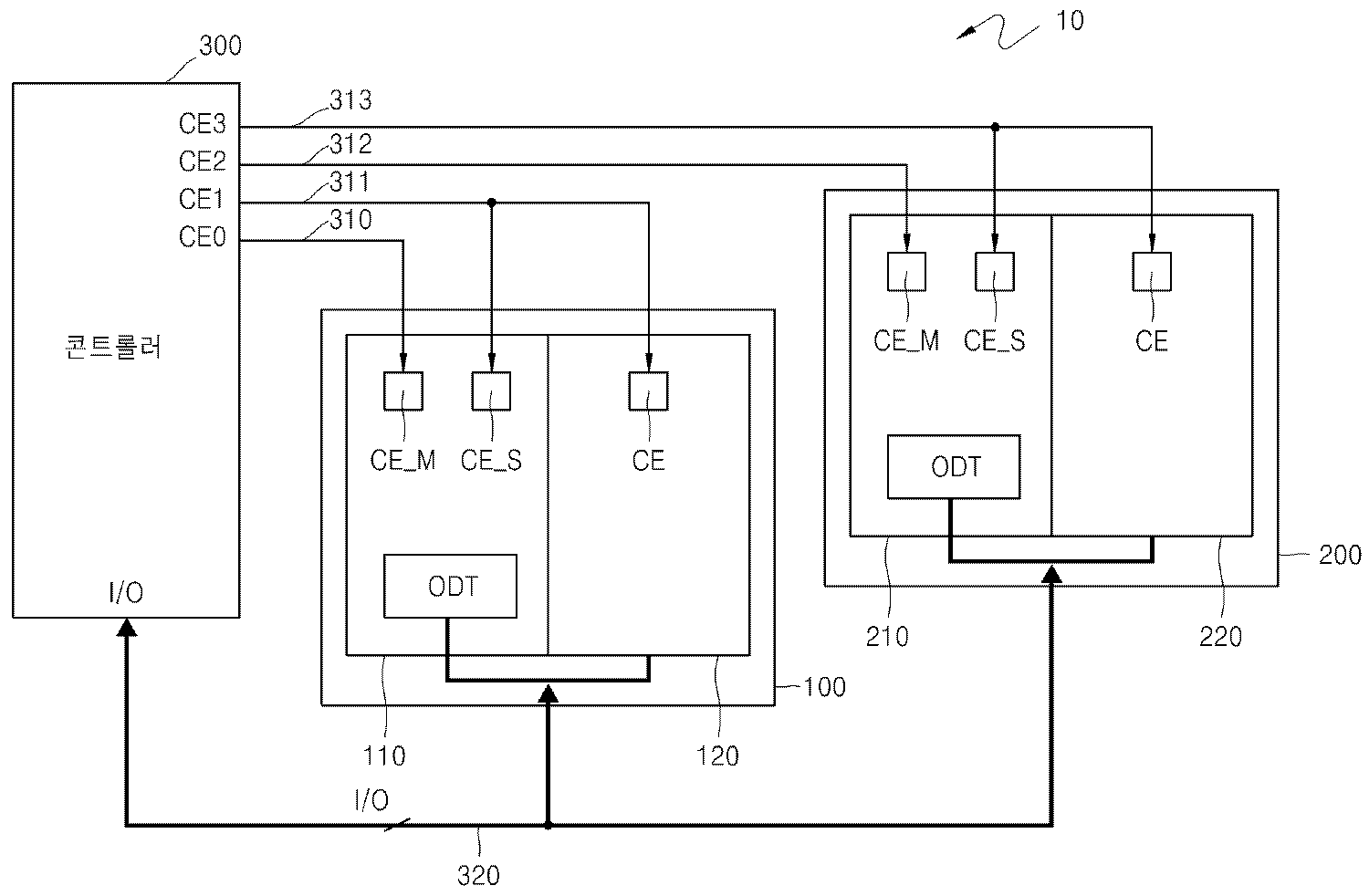
도 1은 본 발명의 일실시예에 따른 반도체 메모리 장치(100, 200)와 결합된 콘트롤러(300)를 구비하는 시스템(10)을 설명하는 도면이다. 도 1을 참조하면, 제1 및 제2 반도체 메모리 장치(100, 200) 각각은 제1 메모리 칩(110, 210)과 제2 메모리 칩(120, 220)을 장착하는 MCP 구조로 이루어진다. 콘트롤러(300)는 다른 경로중에서, 칩 인에이블 신호 라인들(310~313)과 데이터 입출력 라인들(320)에 의해 제1 및 제2 반도체 메모리 장치들(100, 200)과 연결된다. 본 기술 분야의 숙련자들에게 잘 알려진 바와 같이, 시스템(10)은 도시되지 않은 다른 구성 요소와 다른 버스를 포함할 수 있다. 본 발명의 사상에 따라 실시예를 이해하기 위한 구성 요소들에 초점을 맞춘다.1 is a diagram illustrating a
제1 반도체 메모리 장치(110)는, 칩 인에이블 신호 라인들(310, 311)을 통하여 전달되는 제1 및 제2 칩 인에이블 신호들(CE0, CE1)에 의해 각각 억세스되는 제1 메모리 칩(110)과 제2 메모리 칩(120)을 포함한다. 제1 메모리 칩(110)은 2개의 칩 인에이블 포트들(CE_M, CE_S)와 액티브 터미네이션(ODT)을 포함한다. 제2 메모리 칩(120)은 1개의 칩 인에이블 포트(CE)를 포함한다.The first
제1 메모리 칩(110) 내 제1 칩 인에이블 포트(CE_M)는 제1 메모리 칩(110) 자신의 제1 칩 인에이블 신호(CE0)를 수신하고, 제2 칩 인에이블 포트(CE_S)는 제1 반도체 메모리 장치(100) 내 다른 칩, 즉 제2 메모리 칩(120)의 제2 칩 인에이블 신호(CE1)를 수신한다. 제2 메모리 칩(120) 내 칩 인에이블 포트(CE)는 제2 메모리 칩(120) 자신의 제2 칩 인에이블 신호(CE1)를 수신한다. 제1 메모리 칩(110) 내 제1 칩 인에이블 포트(CE_M)는 MCP 구조에서 자신의 메모리 칩이 억세스되었는지 여부를 판단하고, 제2 칩 인에이블 포트(CE_S)는 MCP 구조 내 다른 메모리 칩이 억세스되었는지 여부를 모니터링하는 기능을 갖는다.The first chip enable port CE_M in the
제1 메모리 칩(110) 내 액티브 터미네이션(ODT)은 제1 및 제2 칩 인에이블 포트들(CE_M, CE_S)에 결합된다. 제1 메모리 칩(110) 내 액티브 터미네이션(ODT)은, 제1 칩 인에이블 포트(CE_M) 또는 제2 칩 인에이블 포트(CE_S) 중 어느 하나라도 활성화되면, 오프된다. 이는, 제1 및 제2 메모리 칩들(110, 120) 중 어느 하나라도 억세스되는 경우에, 액티브 터미네이션(ODT)이 오프됨을 의미한다.Active termination (ODT) in the
그리고, 제1 및 제2 메모리 칩들(110, 120) 모두 억세스되지 않는 경우, 제1 메모리 칩(110) 내 제1 칩 인에이블 포트(CE_M) 및 제2 칩 인에이블 포트(CE_S) 모두 비활성화되어, 제1 메모리 칩(110) 내 액티브 터미네이션(ODT)은 온된다.If neither of the first and
즉, 제1 반도체 메모리 장치(100)는, 표 1과 같이, 데이터 입출력 라인들(320)을 공유하는 제1 및 제2 메모리 칩들(110, 120) 중 어느 하나라도 억세스되는 경우에 제1 메모리 칩(110) 내 액티브 터미네이션(ODT)이 오프되고, 제1 및 제2 메모리 칩들(110, 120) 모두 억세스되지 않는 경우에 제1 메모리 칩(110) 내 액티브 터미네이션(ODT)은 온된다.That is, when any one of the first and
ODT decision
제2 반도체 메모리 장치(200)는, 제1 반도체 메모리 장치(100)와 유사하게, 칩 인에이블 신호 라인들(312, 313)을 통하여 전달되는 제3 및 제4 칩 인에이블 신호들(CE2, CE3)에 의해 각각 억세스되는 제3 메모리 칩(210)과 제4 메모리 칩(220)을 포함하고, 제3 메모리 칩(210)은 2개의 칩 인에이블 포트들(CE_M, CE_S)와 액티브 터미네이션(ODT)을 포함한다. 제4 메모리 칩(220)은 1개의 칩 인에이블 포트(CE)를 포함한다. 제3 메모리 칩(210) 내 제1 칩 인에이블 포트(CE_M)는 제3 메모리 칩(310) 자신의 제3 칩 인에이블 신호(CE2)를 수신하고, 제2 칩 인에이블 포트(CE_S)는 제4 메모리 칩(220)의 제4 칩 인에이블 신호(CE3)를 수신한다. 제4 메모리 칩(220) 내 칩 인에이블 포트(CE)는 제4 메모리 칩(220) 자신의 제4 칩 인에이블 신호(CE3)를 수신한다.Similarly to the first
제2 반도체 메모리 장치(200)는, 데이터 입출력 라인들(320)을 공유하는 제3 및 제4 메모리 칩들(210, 220) 중 어느 하나라도 억세스되는 경우에 제3 메모리 칩(210) 내 액티브 터미네이션(ODT)이 오프되고, 제3 및 제4 메모리 칩들(210, 220) 모두 억세스되지 않는 경우에 제3 메모리 칩(210) 내 액티브 터미네이션(ODT)은 온된다.The second
시스템(10)에서, 제1 메모리 칩(110)이 억세스되면, 제1 반도체 메모리 장치(100) 내 제1 메모리 칩(110)들의 액티브 터미네이션(ODT)이 오프되고, 제2 반도체 메모리 장치(200) 내 제3 메모리 칩(210) 내 액티브 터미네이션(ODT)이 온된다. 만약, 제3 메모리 칩(210)이 억세스되면, 제1 반도체 메모리 장치(100) 내 제1 메모리 칩(110)의 액티브 터미네이션(ODT)이 온되고, 제2 반도체 메모리 장치(200) 내 제3 메모리 칩(210) 내 액티브 터미네이션(ODT)이 오프된다. 이에 따라, 콘트롤러(300)로부터의 추가적인 ODT 제어 단자 없이, MCP 구조의 반도체 메모리 장치들(100, 200)의 아더 터미네이션이 구현된다.In the
본 발명은 도면에 도시된 일 실시예를 참고로 설명되었으나 이는 예시적인 것에 불과하며, 본 기술 분야의 통상의 지식을 가진 자라면 이로부터 다양한 변형 및 균등한 타 실시예가 가능하다는 점을 이해할 것이다. 따라서, 본 발명의 진정한 기술적 보호 범위는 첨부된 등록청구범위의 기술적 사상에 의해 정해져야 할 것이다.While the present invention has been particularly shown and described with reference to exemplary embodiments thereof, it is to be understood that the invention is not limited to the disclosed embodiments, but, on the contrary, is intended to cover various modifications and equivalent arrangements included within the spirit and scope of the appended claims. Accordingly, the true scope of the present invention should be determined by the technical idea of the appended claims.
도 1은 본 발명의 일실시예에 따른 반도체 메모리 장치와 결합된 콘트롤러를 구비하는 시스템을 설명하는 도면이다.1 is a diagram illustrating a system including a controller coupled to a semiconductor memory device according to an embodiment of the present invention.
Claims (9)
Priority Applications (2)
| Application Number | Priority Date | Filing Date | Title |
|---|---|---|---|
| KR1020090021240A KR101606452B1 (en) | 2009-03-12 | 2009-03-12 | Semiconductor memory device having multi-chip package for implementing other termination and termination control method thereof |
| US12/717,246 US8315122B2 (en) | 2009-03-12 | 2010-03-04 | Multi-chip package semiconductor memory device providing active termination control |
Applications Claiming Priority (1)
| Application Number | Priority Date | Filing Date | Title |
|---|---|---|---|
| KR1020090021240A KR101606452B1 (en) | 2009-03-12 | 2009-03-12 | Semiconductor memory device having multi-chip package for implementing other termination and termination control method thereof |
Publications (2)
| Publication Number | Publication Date |
|---|---|
| KR20100102924A KR20100102924A (en) | 2010-09-27 |
| KR101606452B1 true KR101606452B1 (en) | 2016-03-28 |
Family
ID=42730575
Family Applications (1)
| Application Number | Title | Priority Date | Filing Date |
|---|---|---|---|
| KR1020090021240A Active KR101606452B1 (en) | 2009-03-12 | 2009-03-12 | Semiconductor memory device having multi-chip package for implementing other termination and termination control method thereof |
Country Status (2)
| Country | Link |
|---|---|
| US (1) | US8315122B2 (en) |
| KR (1) | KR101606452B1 (en) |
Cited By (1)
| Publication number | Priority date | Publication date | Assignee | Title |
|---|---|---|---|---|
| US10734041B2 (en) | 2018-12-24 | 2020-08-04 | SK Hynix Inc. | Semiconductor apparatus related to termination and semiconductor system including the semiconductor apparatus |
Families Citing this family (16)
| Publication number | Priority date | Publication date | Assignee | Title |
|---|---|---|---|---|
| US9153296B2 (en) * | 2010-06-28 | 2015-10-06 | Intel Corporation | Methods and apparatuses for dynamic memory termination |
| US8274308B2 (en) * | 2010-06-28 | 2012-09-25 | Intel Corporation | Method and apparatus for dynamic memory termination |
| KR101294853B1 (en) | 2010-10-21 | 2013-08-08 | 엘지디스플레이 주식회사 | Organic Light Emitting Display Device |
| KR20120077049A (en) | 2010-12-30 | 2012-07-10 | 에스케이하이닉스 주식회사 | System and package including a plurality of chips and controller |
| WO2012106131A1 (en) | 2011-02-02 | 2012-08-09 | Rambus Inc. | On-die termination |
| US8937490B2 (en) * | 2011-10-24 | 2015-01-20 | Samsung Electronics Co., Ltd. | Output driver, devices having the same, and ground termination |
| KR20130045144A (en) * | 2011-10-24 | 2013-05-03 | 삼성전자주식회사 | Output driver, devices having the same, and ground termination |
| US8928349B2 (en) | 2012-07-25 | 2015-01-06 | Samsung Electronics Co., Ltd. | On-die termination circuit, semiconductor memory device and memory system |
| KR20140069650A (en) | 2012-11-29 | 2014-06-10 | 에스케이하이닉스 주식회사 | Integrated circuit and operation method for the same |
| KR102229942B1 (en) | 2014-07-09 | 2021-03-22 | 삼성전자주식회사 | Method of operating multi channel semiconductor device having multi dies and therefore semiconductor device |
| KR102275812B1 (en) * | 2015-09-04 | 2021-07-14 | 삼성전자주식회사 | Semiconductor memory device for improving signal integrity issue in center pad type of stacked chip structure |
| KR102553266B1 (en) | 2017-11-03 | 2023-07-07 | 삼성전자 주식회사 | Memory device including on-die-termination circuit |
| US11003386B2 (en) | 2017-11-22 | 2021-05-11 | Micron Technology, Inc. | Methods for on-die memory termination and memory devices and systems employing the same |
| US11508415B2 (en) * | 2021-03-15 | 2022-11-22 | Transcend Information, Inc. | Semiconductor memory package structure and semiconductor memory system |
| TWI831035B (en) | 2021-08-02 | 2024-02-01 | 瑞昱半導體股份有限公司 | Semiconductor device, data storage system and method for controlling termination circuits |
| CN115938409A (en) * | 2021-08-06 | 2023-04-07 | 瑞昱半导体股份有限公司 | Semiconductor device, data storage system, and terminal circuit control method |
Citations (2)
| Publication number | Priority date | Publication date | Assignee | Title |
|---|---|---|---|---|
| US6717832B2 (en) * | 2001-07-27 | 2004-04-06 | Infineon Technologies Ag | Method for data communication between a plurality of semiconductor modules and a controller module and semiconductor module configured for that purpose |
| US20060262586A1 (en) | 2004-03-05 | 2006-11-23 | Solomon Jeffrey C | Memory module with a circuit providing load isolation and memory domain translation |
Family Cites Families (3)
| Publication number | Priority date | Publication date | Assignee | Title |
|---|---|---|---|---|
| KR100389928B1 (en) * | 2001-07-20 | 2003-07-04 | 삼성전자주식회사 | Semiconductor memory system for controlling active termination |
| US7142461B2 (en) * | 2002-11-20 | 2006-11-28 | Micron Technology, Inc. | Active termination control though on module register |
| US7952944B2 (en) * | 2008-04-30 | 2011-05-31 | International Business Machines Corporation | System for providing on-die termination of a control signal bus |
-
2009
- 2009-03-12 KR KR1020090021240A patent/KR101606452B1/en active Active
-
2010
- 2010-03-04 US US12/717,246 patent/US8315122B2/en active Active
Patent Citations (2)
| Publication number | Priority date | Publication date | Assignee | Title |
|---|---|---|---|---|
| US6717832B2 (en) * | 2001-07-27 | 2004-04-06 | Infineon Technologies Ag | Method for data communication between a plurality of semiconductor modules and a controller module and semiconductor module configured for that purpose |
| US20060262586A1 (en) | 2004-03-05 | 2006-11-23 | Solomon Jeffrey C | Memory module with a circuit providing load isolation and memory domain translation |
Cited By (1)
| Publication number | Priority date | Publication date | Assignee | Title |
|---|---|---|---|---|
| US10734041B2 (en) | 2018-12-24 | 2020-08-04 | SK Hynix Inc. | Semiconductor apparatus related to termination and semiconductor system including the semiconductor apparatus |
Also Published As
| Publication number | Publication date |
|---|---|
| US8315122B2 (en) | 2012-11-20 |
| US20100232196A1 (en) | 2010-09-16 |
| KR20100102924A (en) | 2010-09-27 |
Similar Documents
| Publication | Publication Date | Title |
|---|---|---|
| KR101606452B1 (en) | Semiconductor memory device having multi-chip package for implementing other termination and termination control method thereof | |
| US12395173B2 (en) | Integrated circuit that applies different data interface terminations during and after write data reception | |
| US11625345B2 (en) | Methods, flash memory controller, and electronic device for SD memory card device | |
| KR101026677B1 (en) | Integrated circuits, methods and systems | |
| US7342411B2 (en) | Dynamic on-die termination launch latency reduction | |
| KR100932806B1 (en) | Dynamic on-die terminations per byte lane | |
| KR100951091B1 (en) | Integrated circuits, methods and systems | |
| US20120059977A1 (en) | Electronic device, controller for accessing a plurality of chips via at least one bus, and method for accessing a plurality of chips via at least one bus | |
| US12340123B2 (en) | Memory systems, modules, and methods for improved capacity | |
| KR100439089B1 (en) | Data processing systems, external device access methods, and data processors | |
| US10153759B2 (en) | Control chip and control system utilizing the same | |
| USRE43162E1 (en) | Semiconductor memory module, electronic apparatus and method for operating thereof | |
| JPS6177770A (en) | Semiconductor integrated circuit device |
Legal Events
| Date | Code | Title | Description |
|---|---|---|---|
| PA0109 | Patent application |
St.27 status event code: A-0-1-A10-A12-nap-PA0109 |
|
| PG1501 | Laying open of application |
St.27 status event code: A-1-1-Q10-Q12-nap-PG1501 |
|
| R18-X000 | Changes to party contact information recorded |
St.27 status event code: A-3-3-R10-R18-oth-X000 |
|
| A201 | Request for examination | ||
| PA0201 | Request for examination |
St.27 status event code: A-1-2-D10-D11-exm-PA0201 |
|
| D13-X000 | Search requested |
St.27 status event code: A-1-2-D10-D13-srh-X000 |
|
| D14-X000 | Search report completed |
St.27 status event code: A-1-2-D10-D14-srh-X000 |
|
| E902 | Notification of reason for refusal | ||
| PE0902 | Notice of grounds for rejection |
St.27 status event code: A-1-2-D10-D21-exm-PE0902 |
|
| P11-X000 | Amendment of application requested |
St.27 status event code: A-2-2-P10-P11-nap-X000 |
|
| P13-X000 | Application amended |
St.27 status event code: A-2-2-P10-P13-nap-X000 |
|
| E701 | Decision to grant or registration of patent right | ||
| PE0701 | Decision of registration |
St.27 status event code: A-1-2-D10-D22-exm-PE0701 |
|
| GRNT | Written decision to grant | ||
| PR0701 | Registration of establishment |
St.27 status event code: A-2-4-F10-F11-exm-PR0701 |
|
| PR1002 | Payment of registration fee |
St.27 status event code: A-2-2-U10-U11-oth-PR1002 Fee payment year number: 1 |
|
| PG1601 | Publication of registration |
St.27 status event code: A-4-4-Q10-Q13-nap-PG1601 |
|
| FPAY | Annual fee payment |
Payment date: 20190228 Year of fee payment: 4 |
|
| PR1001 | Payment of annual fee |
St.27 status event code: A-4-4-U10-U11-oth-PR1001 Fee payment year number: 4 |
|
| FPAY | Annual fee payment |
Payment date: 20200228 Year of fee payment: 5 |
|
| PR1001 | Payment of annual fee |
St.27 status event code: A-4-4-U10-U11-oth-PR1001 Fee payment year number: 5 |
|
| PR1001 | Payment of annual fee |
St.27 status event code: A-4-4-U10-U11-oth-PR1001 Fee payment year number: 6 |
|
| PR1001 | Payment of annual fee |
St.27 status event code: A-4-4-U10-U11-oth-PR1001 Fee payment year number: 7 |
|
| PR1001 | Payment of annual fee |
St.27 status event code: A-4-4-U10-U11-oth-PR1001 Fee payment year number: 8 |
|
| PR1001 | Payment of annual fee |
St.27 status event code: A-4-4-U10-U11-oth-PR1001 Fee payment year number: 9 |
|
| PR1001 | Payment of annual fee |
St.27 status event code: A-4-4-U10-U11-oth-PR1001 Fee payment year number: 10 |
|
| P22-X000 | Classification modified |
St.27 status event code: A-4-4-P10-P22-nap-X000 |