KR101570881B1 - Solar cell and manufacturing method thereof - Google Patents
Solar cell and manufacturing method thereof Download PDFInfo
- Publication number
- KR101570881B1 KR101570881B1 KR1020090067646A KR20090067646A KR101570881B1 KR 101570881 B1 KR101570881 B1 KR 101570881B1 KR 1020090067646 A KR1020090067646 A KR 1020090067646A KR 20090067646 A KR20090067646 A KR 20090067646A KR 101570881 B1 KR101570881 B1 KR 101570881B1
- Authority
- KR
- South Korea
- Prior art keywords
- conductive material
- conductive layer
- photoelectric conversion
- printing speed
- solar cell
- Prior art date
Links
- 238000004519 manufacturing process Methods 0.000 title claims abstract description 18
- 238000007639 printing Methods 0.000 claims abstract description 70
- 239000004020 conductor Substances 0.000 claims abstract description 57
- 238000006243 chemical reaction Methods 0.000 claims abstract description 56
- 238000000034 method Methods 0.000 claims description 18
- 239000000463 material Substances 0.000 claims description 6
- 238000003892 spreading Methods 0.000 abstract description 6
- XUIMIQQOPSSXEZ-UHFFFAOYSA-N Silicon Chemical compound [Si] XUIMIQQOPSSXEZ-UHFFFAOYSA-N 0.000 abstract 1
- 229910052710 silicon Inorganic materials 0.000 abstract 1
- 239000010703 silicon Substances 0.000 abstract 1
- 229910021417 amorphous silicon Inorganic materials 0.000 description 19
- 230000000052 comparative effect Effects 0.000 description 13
- 229910021421 monocrystalline silicon Inorganic materials 0.000 description 11
- 238000007650 screen-printing Methods 0.000 description 6
- 239000004065 semiconductor Substances 0.000 description 5
- 239000000839 emulsion Substances 0.000 description 4
- 238000010438 heat treatment Methods 0.000 description 4
- 239000000969 carrier Substances 0.000 description 3
- 239000002904 solvent Substances 0.000 description 3
- 238000005229 chemical vapour deposition Methods 0.000 description 2
- 230000007423 decrease Effects 0.000 description 2
- 230000003247 decreasing effect Effects 0.000 description 2
- 238000010586 diagram Methods 0.000 description 2
- 238000005259 measurement Methods 0.000 description 2
- 238000007645 offset printing Methods 0.000 description 2
- 239000002245 particle Substances 0.000 description 2
- 230000000704 physical effect Effects 0.000 description 2
- 238000004544 sputter deposition Methods 0.000 description 2
- BQCADISMDOOEFD-UHFFFAOYSA-N Silver Chemical compound [Ag] BQCADISMDOOEFD-UHFFFAOYSA-N 0.000 description 1
- 239000011230 binding agent Substances 0.000 description 1
- 230000015572 biosynthetic process Effects 0.000 description 1
- 239000000919 ceramic Substances 0.000 description 1
- 239000011248 coating agent Substances 0.000 description 1
- 238000000576 coating method Methods 0.000 description 1
- 239000013078 crystal Substances 0.000 description 1
- 230000007547 defect Effects 0.000 description 1
- 230000000694 effects Effects 0.000 description 1
- 238000005516 engineering process Methods 0.000 description 1
- 238000005530 etching Methods 0.000 description 1
- 239000010408 film Substances 0.000 description 1
- 230000031700 light absorption Effects 0.000 description 1
- 238000005268 plasma chemical vapour deposition Methods 0.000 description 1
- 229910021420 polycrystalline silicon Inorganic materials 0.000 description 1
- 239000011347 resin Substances 0.000 description 1
- 229920005989 resin Polymers 0.000 description 1
- 229910052709 silver Inorganic materials 0.000 description 1
- 239000004332 silver Substances 0.000 description 1
- 239000000758 substrate Substances 0.000 description 1
- 239000010409 thin film Substances 0.000 description 1
Images


Classifications
-
- H—ELECTRICITY
- H10—SEMICONDUCTOR DEVICES; ELECTRIC SOLID-STATE DEVICES NOT OTHERWISE PROVIDED FOR
- H10F—INORGANIC SEMICONDUCTOR DEVICES SENSITIVE TO INFRARED RADIATION, LIGHT, ELECTROMAGNETIC RADIATION OF SHORTER WAVELENGTH OR CORPUSCULAR RADIATION
- H10F77/00—Constructional details of devices covered by this subclass
- H10F77/20—Electrodes
- H10F77/206—Electrodes for devices having potential barriers
- H10F77/211—Electrodes for devices having potential barriers for photovoltaic cells
-
- B—PERFORMING OPERATIONS; TRANSPORTING
- B41—PRINTING; LINING MACHINES; TYPEWRITERS; STAMPS
- B41F—PRINTING MACHINES OR PRESSES
- B41F15/00—Screen printers
- B41F15/14—Details
- B41F15/44—Squeegees or doctors
-
- H—ELECTRICITY
- H10—SEMICONDUCTOR DEVICES; ELECTRIC SOLID-STATE DEVICES NOT OTHERWISE PROVIDED FOR
- H10F—INORGANIC SEMICONDUCTOR DEVICES SENSITIVE TO INFRARED RADIATION, LIGHT, ELECTROMAGNETIC RADIATION OF SHORTER WAVELENGTH OR CORPUSCULAR RADIATION
- H10F10/00—Individual photovoltaic cells, e.g. solar cells
- H10F10/10—Individual photovoltaic cells, e.g. solar cells having potential barriers
- H10F10/16—Photovoltaic cells having only PN heterojunction potential barriers
- H10F10/164—Photovoltaic cells having only PN heterojunction potential barriers comprising heterojunctions with Group IV materials, e.g. ITO/Si or GaAs/SiGe photovoltaic cells
- H10F10/165—Photovoltaic cells having only PN heterojunction potential barriers comprising heterojunctions with Group IV materials, e.g. ITO/Si or GaAs/SiGe photovoltaic cells the heterojunctions being Group IV-IV heterojunctions, e.g. Si/Ge, SiGe/Si or Si/SiC photovoltaic cells
- H10F10/166—Photovoltaic cells having only PN heterojunction potential barriers comprising heterojunctions with Group IV materials, e.g. ITO/Si or GaAs/SiGe photovoltaic cells the heterojunctions being Group IV-IV heterojunctions, e.g. Si/Ge, SiGe/Si or Si/SiC photovoltaic cells the Group IV-IV heterojunctions being heterojunctions of crystalline and amorphous materials, e.g. silicon heterojunction [SHJ] photovoltaic cells
-
- H—ELECTRICITY
- H10—SEMICONDUCTOR DEVICES; ELECTRIC SOLID-STATE DEVICES NOT OTHERWISE PROVIDED FOR
- H10F—INORGANIC SEMICONDUCTOR DEVICES SENSITIVE TO INFRARED RADIATION, LIGHT, ELECTROMAGNETIC RADIATION OF SHORTER WAVELENGTH OR CORPUSCULAR RADIATION
- H10F71/00—Manufacture or treatment of devices covered by this subclass
-
- Y—GENERAL TAGGING OF NEW TECHNOLOGICAL DEVELOPMENTS; GENERAL TAGGING OF CROSS-SECTIONAL TECHNOLOGIES SPANNING OVER SEVERAL SECTIONS OF THE IPC; TECHNICAL SUBJECTS COVERED BY FORMER USPC CROSS-REFERENCE ART COLLECTIONS [XRACs] AND DIGESTS
- Y02—TECHNOLOGIES OR APPLICATIONS FOR MITIGATION OR ADAPTATION AGAINST CLIMATE CHANGE
- Y02E—REDUCTION OF GREENHOUSE GAS [GHG] EMISSIONS, RELATED TO ENERGY GENERATION, TRANSMISSION OR DISTRIBUTION
- Y02E10/00—Energy generation through renewable energy sources
- Y02E10/50—Photovoltaic [PV] energy
Landscapes
- Engineering & Computer Science (AREA)
- Mechanical Engineering (AREA)
- Photovoltaic Devices (AREA)
- Life Sciences & Earth Sciences (AREA)
- Sustainable Energy (AREA)
- Sustainable Development (AREA)
Abstract
본 발명은 도전성 페이스트가 광전 변환부 상에서 번져 퍼지는 것을 억제 가능한 태양 전지의 제조 방법을 제공하는 것이다. 태양 전지의 제조 방법에 있어서, 제1 도전성 재료가 인쇄되는 제1 인쇄 속도는, 상기 제1 도전성 재료 상에 형성되는 제2 도전성 재료가 인쇄되는 제2 인쇄 속도보다도 빠르다.The present invention provides a method of manufacturing a solar cell capable of suppressing spreading of a conductive paste on a photoelectric conversion portion. In the method of manufacturing a solar cell, the first printing speed at which the first conductive material is printed is faster than the second printing speed at which the second conductive material formed on the first conductive material is printed.
태양 전지, 광전 변환부, 세선 전극, 실리콘 웨이퍼, 도전층 Solar cell, photoelectric conversion portion, fine wire electrode, silicon wafer, conductive layer
Description
<관련 기술><Related Technology>
2008년 7월 25일에 제출된 일본 출원 제2008-192701호, 발명의 명칭「태양 전지의 제조 방법」은, 여기에 35USC119에 기초하여 우선권의 이익을 주장하는 동시에, 이 모든 내용이 참고로서 인용된다.Japanese Patent Application No. 2008-192701, filed on July 25, 2008, entitled " Method of Manufacturing a Solar Cell ", claims the benefit of priority based on 35 USC 119, do.
본 발명은, 광전 변환 상에 설치되는 복수개의 세선 전극을 구비하는 태양 전지 및 그 제조 방법에 관한 것이다.The present invention relates to a solar cell having a plurality of fine-line electrodes provided on a photoelectric conversion and a manufacturing method thereof.
태양 전지는 클린하고 무진장하게 공급되는 태양광 에너지를 직접 전기 에너지로 변환할 수 있으므로, 새로운 에너지원으로서 기대되고 있다.Solar cells are expected to be a new source of energy because they can convert solar energy, which is clean and inexhaustible, directly into electrical energy.
일반적으로, 태양 전지는 수광에 의해 광 생성 캐리어를 생성하는 광전 변환부와, 광전 변환부로부터 광 생성 캐리어를 수집하는 복수개의 세선 전극을 구비한다. 각 세선 전극은, 스크린 인쇄법이나 오프셋 인쇄법 등의 인쇄법에 의해, 도전성 페이스트를 광전 변환부 상에 인쇄함으로써 형성된다.Generally, a solar cell has a photoelectric conversion unit that generates a photogenerated carrier by light reception, and a plurality of fine-line electrodes that collect photogenerated carriers from the photoelectric conversion unit. Each fine wire electrode is formed by printing a conductive paste on a photoelectric conversion portion by a printing method such as a screen printing method or an offset printing method.
여기서, 스크린 인쇄법에 의해 도전성 페이스트를 복수회 겹쳐 인쇄함으로써 각 세선 전극을 형성하는 방법이 제안되어 있다(특허 문헌 1 참조). 이 방법에 따 르면, 각 세선 전극의 표면을 평탄하게 할 수 있으므로, 저온 환경에서 사용되는 고저항의 도전성 페이스트를 사용해도 각 세선 전극의 전기 저항이 커지는 것을 억제할 수 있다.Here, a method of forming fine-line electrodes by overlaying a conductive paste by a screen printing method a plurality of times has been proposed (see Patent Document 1). According to this method, since the surface of each fine wire electrode can be flattened, the electric resistance of each fine wire electrode can be suppressed from increasing even when a high-resistance conductive paste used in a low temperature environment is used.
특허 문헌 1 : 일본 특허 공개 평11-103084호 공보Patent Document 1: JP-A-11-103084
그러나, 광전 변환부 상에 인쇄된 도전성 페이스트는 유동성을 가지므로, 도전성 페이스트가 광전 변환부 상에서 번져 퍼진다는 문제가 있었다. 이와 같이, 도전성 페이스트가 광전 변환부 상에서 번져 퍼지면 세선 전극의 선 폭이 커지기 때문에, 광전 변환부의 수광 면적이 감소하게 된다.However, since the conductive paste printed on the photoelectric conversion portion has fluidity, there is a problem that the conductive paste spreads on the photoelectric conversion portion. Thus, when the conductive paste spreads on the photoelectric conversion portion, the line width of the fine line electrode becomes large, so that the light receiving area of the photoelectric conversion portion is reduced.
특히, 이와 같은 문제는, 광전 변환부에 있어서의 광의 흡수 효율을 향상시키는 것을 목적으로 하여 광전 변환부의 표면에 복수의 볼록부를 형성한 경우에 발생하기 쉽다. 구체적으로는, 도전성 페이스트는, 각 볼록부 사이의 공간(골부)을 따라 번져 퍼진다.Particularly, such a problem is liable to occur when a plurality of convex portions are formed on the surface of the photoelectric conversion portion for the purpose of improving the light absorption efficiency in the photoelectric conversion portion. Specifically, the conductive paste spreads along spaces (valleys) between the convex portions.
본 발명은 상기의 문제를 감안하여 이루어진 것으로, 도전성 페이스트가 광전 변환부 상에서 번져 퍼지는 것을 억제 가능한 태양 전지의 제조 방법을 제공하는 것을 목적으로 한다.SUMMARY OF THE INVENTION The present invention has been made in view of the above problems, and an object of the present invention is to provide a manufacturing method of a solar cell capable of suppressing spreading of a conductive paste on a photoelectric conversion portion.
본 발명의 특징에 관한 태양 전지의 제조 방법은, 광전 변환부와, 상기 광전 변환부 상에 순차적으로 형성된 제1 도전층 및 제2 도전층을 각각 포함하는 복수개의 세선 전극을 구비하는 태양 전지의 제조 방법이며, 상기 광전 변환부 상에 제1 도전성 재료를 제1 인쇄 속도로 인쇄함으로써 상기 제1 도전층을 형성하는 단계와, 상기 제1 도전층 상에 제2 도전성 재료를 제2 인쇄 속도로 인쇄함으로써 상기 제2 도전층을 형성하는 단계를 구비하고, 상기 제1 도전성 재료를 인쇄하는 제1 인쇄 속도는 상기 제2 도전성 재료를 인쇄하는 제2 인쇄 속도보다도 빠르다.A manufacturing method of a solar cell according to a feature of the present invention is a manufacturing method of a solar cell including a photoelectric conversion portion and a plurality of fine wire electrodes each including a first conductive layer and a second conductive layer sequentially formed on the photoelectric conversion portion The method comprising: forming the first conductive layer by printing a first conductive material on the photoelectric conversion portion at a first printing speed; forming a second conductive material on the first conductive layer at a second printing speed And forming the second conductive layer by printing, wherein the first printing speed for printing the first conductive material is faster than the second printing speed for printing the second conductive material.
상기 태양 전지의 제조 방법에 따르면, 제1 인쇄 속도를 제2 인쇄 속도보다 빠르게 하기 위해, 제1 도전성 재료의 양을 적게 할 수 있다. 따라서, 제1 도전성 재료가 광전 변환부 상에서 번져 퍼지는 것을 억제할 수 있다. 또한, 제2 인쇄 속도를 제1 인쇄 속도보다도 느리게 하기 위해, 제2 도전성 재료의 양을 많게 하는 동시에, 제1 도전성 재료에 의한 표면 장력에 의해 제2 도전층의 선 폭을 작게 유지할 수 있다. 그 결과, 각 세선 전극의 높이를 크게 할 수 있으므로, 각 세선 전극의 전기 저항을 작게 할 수 있다.According to the manufacturing method of the solar cell, the amount of the first conductive material can be reduced in order to make the first printing speed faster than the second printing speed. Therefore, it is possible to suppress spreading of the first conductive material on the photoelectric conversion portion. Further, in order to make the second printing speed slower than the first printing speed, the amount of the second conductive material may be increased and the line width of the second conductive layer may be kept small by surface tension by the first conductive material. As a result, since the height of each fine wire electrode can be increased, the electrical resistance of each fine wire electrode can be reduced.
또한, 상기 제1 도전층을 형성한 후에, 상기 제1 도전층을 가열 처리하는 것이 바람직하다.Further, it is preferable that the first conductive layer is subjected to heat treatment after the first conductive layer is formed.
상기에 따르면, 전성 페이스트가 광전 변환부 상에서 번져 퍼지는 것을 억제가능한 태양 전지의 제조 방법을 제공할 수 있다.According to the above, it is possible to provide a method of manufacturing a solar cell capable of suppressing spreading of a conductive paste on a photoelectric conversion portion.
다음에, 도면을 사용하여 본 발명의 실시 형태에 대해 설명한다. 이하의 도면의 기재에 있어서, 동일 또는 유사 부분에는, 동일 또는 유사 부호를 부여하고 있다. 단, 도면은 모식적인 것이며, 각 치수의 비율 등은 현실의 것과는 다른 것에 유의해야 한다. 따라서, 구체적인 치수 등은 이하의 설명을 참작하여 판단해야 하는 것이다. 또한, 도면 상호간에 있어서도 서로의 치수의 관계나 비율이 다른 부분이 포함되어 있는 것은 물론이다.Next, an embodiment of the present invention will be described with reference to the drawings. In the following description of the drawings, the same or similar parts are denoted by the same or similar reference numerals. However, it should be noted that the drawings are schematic, and the ratios of the respective dimensions and the like are different from those of the real world. Therefore, specific dimensions and the like should be judged based on the following description. Needless to say, the drawings also include portions having different dimensions and relative ratios.
여기서, 용어 "상에" 등은 예를 들어 층의 표면에 의해 정의되고, 공간에 있어서의 표면의 방향과는 무관하다. 용어 "상에"는 명세서나 청구 범위에 있어서 어느 층이 다른 층에 접하고 있어도 사용하는 경우가 있고, 어느 층이 다른 층에 접하고 있지 않은 경우, 예를 들어 사이에 층이 있어도 사용하는 경우가 있다.Herein, the term "on" is defined, for example, by the surface of the layer and is independent of the orientation of the surface in space. The term "on" is used in the specification and claims, regardless of which layer is in contact with another layer. In the case where a layer is not in contact with another layer, for example, .
(태양 전지의 구성)(Configuration of solar cell)
이하에 있어서, 본 실시 형태에 관한 태양 전지의 구성에 대해, 도면을 참조하면서 설명한다. 도 1은, 본 실시 형태에 관한 태양 전지(10)의 수광면측의 평면도이다. 도 2는, 도 1의 A-A선에 있어서의 단면도이다.Hereinafter, the structure of the solar cell according to the present embodiment will be described with reference to the drawings. 1 is a plan view of the light receiving surface side of the solar cell 10 according to the present embodiment. 2 is a cross-sectional view taken along the line A-A of Fig.
도 1 및 도 2에 도시하는 바와 같이, 태양 전지(10)는 광전 변환부(20)와, 복수개의 세선 전극(30)과, 접속용 전극(40)을 구비한다.As shown in Figs. 1 and 2, a solar cell 10 includes a
광전 변환부(20)는 태양광이 입사하는 수광면(도 2의 상면)과, 수광면의 반대측에 형성되는 이면(도 2의 하면)을 갖는다. 수광면과 이면은, 태양 전지(10)의 주면(主面)이다.The
광전 변환부(20)는, 반도체 웨이퍼를 사용하여 형성되는 반도체 pn 접합 또는 반도체 pin 접합을 갖고 있고, 수광에 의해 광 생성 캐리어를 생성한다. 광 생성 캐리어라 함은, 태양광이 광전 변환부(20)에 흡수되어 생성되는 정공과 전자를 말한다. 광전 변환부(20)는 단결정 Si, 다결정 Si 등의 결정계 반도체 재료에 의해 구성되는 반도체 웨이퍼를 포함한다. 본 실시 형태에서는, 광전 변환부(20)는 단결정 실리콘 웨이퍼와 비정질 실리콘층 사이에 실질적으로 진성의 비정질 실리콘층을 끼움으로써, 그 계면에서의 결함을 저감시켜, 헤테로 결합 계면의 특성을 개선한 구조, 소위 HIT 구조를 갖는다. 구체적으로는, 도 2에 도시하는 바와 같이, 광전 변환부(20)는, n형 단결정 실리콘 웨이퍼(21)의 한 주면 상에 순차적으로 형성된 i형 비정질 실리콘층(22), p형 비정질 실리콘층(23) 및 ITO층(24)과, n형 단결정 실리콘 웨이퍼(21)의 다른 주면 상에 순차적으로 형성된 i형 비정질 실리콘층(25), n형 비정질 실리콘층(26) 및 ITO층(27)을 구비한다.The
여기서, 도 2에 도시하는 바와 같이, n형 단결정 실리콘 웨이퍼(21)의 한 주면 및 다른 주면에는, 복수의 볼록부(텍스처)가 형성되어 있다.Here, as shown in Fig. 2, a plurality of convex portions (textures) are formed on one main surface and the other main surface of the n-type single crystal silicon wafer 21. [
복수개의 세선 전극(30)은 광전 변환부(20)로부터 광 생성 캐리어를 수집하 는 전극이다. 복수개의 세선 전극(30)은, 도 1에 도시하는 바와 같이 광전 변환부(20)의 수광면 대략 전체 영역에 걸쳐서 형성된다. 복수개의 세선 전극(30)은, 수지 재료를 바인더로 하고, 은 입자 등의 도전성 입자를 필러로 한 수지형 도전성 페이스트나, 소결형 도전성 페이스트(소위, 세라믹 페이스트) 등의 도전성 재료에 의해 형성할 수 있다. 또한, 각 세선 전극(30)의 치수, 형상 및 갯수는, 광전 변환부(20)의 사이즈나 물성 등을 고려하여 적당한 갯수로 설정할 수 있다. 예를 들어, 광전 변환부(20)의 치수가 한변이 약 100㎜인 사각형의 경우에는, 폭 0.03 내지 0.15㎜, 높이 0.01 내지 0.05㎜의 세선 전극(30)을 약 50개 형성할 수 있다.The plurality of
여기서, 본 실시 형태에 있어서, 각 세선 전극(30)은, 도 2에 도시하는 바와 같이, 광전 변환부(20) 상에 순차적으로 형성된 제1 도전층(31) 및 제2 도전층(32)을 포함한다. 제1 도전층(31) 및 제2 도전층(32) 각각은, 인쇄법을 이용하여, 상술한 도전성 재료에 의해 형성된다.2, each
본 실시 형태의 태양 전지는, 광전 변환부(20) 상에 제1 단면적으로 형성된 제1 도전층(31)과, 제1 도전층 상에 제1 단면적보다도 큰 제2 단면적으로 형성된 제2 도전층(32)을 갖는다. 또한, 본 실시 형태의 태양 전지는, 제2 도전층(32)의 높이는 제1 도전층(31)의 높이보다 높다. 또한, 광전 변환부의 표면에는 텍스처가 형성되고, 제1 도전층은 그 표면에 형성된다.The solar cell of this embodiment includes a first
접속용 전극(40)은 복수의 태양 전지(10)를 서로 전기적으로 직렬 또는 병렬로 접속하는 배선재(도시하지 않음)를 접속하기 위한 전극이다. 접속용 전극(40)은 복수개의 세선 전극(30)과 교차하도록 형성되고, 각 세선 전극(30)과 전기적으 로 접속된다. 접속용 전극(40)은 각 세선 전극(30)과 같은 재료를 사용하여 형성할 수 있다. 또한, 접속용 전극(40)의 치수, 형상 및 갯수는, 광전 변환부(20)의 사이즈나 물성 등을 고려하여 적당한 갯수로 설정할 수 있다. 예를 들어, 광전 변환부(20)의 치수가 한변이 약 100㎜인 사각형의 경우에는, 폭 0.3 내지 2.0㎜, 높이 0.01 내지 0.05㎜의 접속용 전극(40)을 2개 형성할 수 있다.The connecting
본 실시 형태에서는, 도 2에 도시하는 바와 같이, 각 세선 전극(30) 및 접속용 전극(40)은 광전 변환부(20)의 이면 상에도 형성되지만, 이에 한정되는 것은 아니다. 예를 들어, 세선 전극(30)은 광전 변환부(20)의 이면 대략 전체면을 덮도록 형성되어 있어도 된다. 본 발명은, 광전 변환부(20)의 이면 상에 형성되는 세선 전극(30) 및 접속용 전극(40)의 형상을 한정하는 것은 아니다.In this embodiment, as shown in Fig. 2, the fine-
(태양 전지의 제조 방법)(Manufacturing Method of Solar Cell)
다음에, 본 실시 형태에 관한 태양 전지(10)의 제조 방법에 대해, 도면을 참조하면서 설명한다.Next, a manufacturing method of the solar cell 10 according to the present embodiment will be described with reference to the drawings.
우선, n형 단결정 실리콘 웨이퍼(21)에 에칭 처리를 실시함으로써, n형 단결정 실리콘 웨이퍼(21)의 표면에 미세한 요철(텍스처)을 형성한다.First, the n-type single crystal silicon wafer 21 is etched to form fine irregularities (textures) on the surface of the n-type single crystal silicon wafer 21.
다음에, n형 단결정 실리콘 웨이퍼의 한 주면 상에 CVD(화학 기상 성장)법을 이용하여, i형 비정질 실리콘층(22), p형 비정질 실리콘층(23)을 순차적으로 형성한다. 마찬가지로, n형 단결정 실리콘 웨이퍼(21)의 다른 주면 상에 i형 비정질 실리콘층(25), n형 비정질 실리콘층(26)을 순차적으로 형성한다.Next, an i-type
다음에, 스퍼터법 등을 이용하여, p형 비정질 실리콘층(23) 상에 ITO층(24) 을 형성하는 동시에, n형 비정질 실리콘층(26) 상에 ITO층(27)을 형성한다.Next, an ITO layer 24 is formed on the p-type
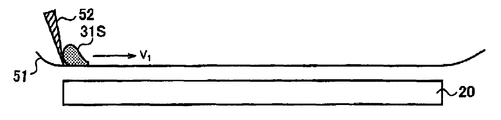
다음에, 스크린 인쇄법을 이용하여, 광전 변환부(20) 상에 제1 도전성 재료(31S)를 인쇄함으로써, 제1 도전층(31)을 형성한다. 구체적으로는, 도 3에 도시하는 바와 같이, 스크린판(51) 상에 배치된 제1 도전성 재료(31S)를 스퀴지(52)에 의해 광전 변환부(20) 상에 압출한다. 스크린판(51)에 있어서, 메쉬 형상의 와이어[사(紗)]를 코팅하는 유제는, 각 세선 전극(30)의 패턴에 대응하도록 제거되어 있다. 제1 도전성 재료(31S)는 스크린판(51) 중 유제가 제거된 영역을 통해 광전 변환부(20) 상에 압출된다.Next, the first
계속해서, 스크린 인쇄법에 의해, 제1 도전층(31) 상에 제2 도전성 재료(32S)를 인쇄함으로써, 제2 도전층(32)을 형성한다. 구체적으로는, 도 4에 도시하는 바와 같이, 스크린판(51) 상에 배치된 제2 도전성 재료(32S)를, 스퀴지(52)에 의해 광전 변환부(20) 상에 압출한다. 제2 도전성 재료(32S)는 스크린판(51) 중 유제가 제거된 영역을 통해 제1 도전층(31) 상에 압출된다. 제1 도전성 재료(31S)는 미건조이므로, 제1 도전층(31) 상에 인쇄된 제2 도전성 재료(32S)에 표면 장력이 작용한다. 도 5는, 광전 변환부(20) 상에 형성된 복수개의 세선 전극(30)을 도시하는 도면이다.Subsequently, the second
여기서, 도 3에 도시하는 바와 같이, 제1 도전성 재료(31S)가 인쇄되는 제1 인쇄 속도(V1)는 스퀴지(52)의 이동 속도이다. 또한, 도 4에 도시하는 바와 같이, 제2 도전성 재료(32S)가 인쇄되는 제2 인쇄 속도(V2)는 스퀴지(52)의 이동 속도이다. 본 실시 형태에서는, 제1 인쇄 속도(V1)는 제2 인쇄 속도(V2)보다도 빠르다.Here, as shown in Fig. 3, the first printing speed V1 at which the first conductive material 31S is printed is the moving speed of the
제1 인쇄 속도(V1) 및 제2 인쇄 속도(V2)는, 예를 들어 30 내지 200㎜/sec로 설정할 수 있지만, 이에 한정되는 것이 아니다. 제1 인쇄 속도(V1) 및 제2 인쇄 속도(V2)는 제1 도전성 재료(31S) 및 제2 도전성 재료(32S)의 점도나 각 세선 전극(30)의 선 폭에 따라서 적절하게 설정되는 것이 바람직하다.The first printing speed V1 and the second printing speed V2 can be set to, for example, 30 to 200 mm / sec, but are not limited thereto. The first printing speed V1 and the second printing speed V2 are appropriately set in accordance with the viscosity of the first conductive material 31S and the second
또한, 접속용 전극(40)은 복수개의 세선 전극(30)의 형성과 동시에 형성할 수 있다. 이 경우, 접속용 전극(40)에 대응하는 패턴으로 유제가 제거되어 있으면 된다.Further, the
다음에, 백 수십도로 가열함으로써, 제1 도전성 재료(31S) 및 제2 도전성 재료(32S)를 경화시킨다.Next, the first conductive material 31S and the second
(작용ㆍ효과)(Action / effect)
본 실시 형태에 관한 태양 전지(10)의 제조 방법에 있어서, 제1 도전성 재료(31S)가 인쇄되는 제1 인쇄 속도(V1)는 제2 도전성 재료(32S)가 인쇄되는 제2 인쇄 속도(V2)보다도 빠르다.In the method of manufacturing the solar cell 10 according to the present embodiment, the first printing speed V1 at which the first conductive material 31S is printed is the second printing speed V2 at which the second
여기서, 제1 인쇄 속도(V1)와 제1 도전층(31)의 선 폭과의 관계와, 제2 인쇄 속도(V2)와 제2 도전층(32)의 선 폭과의 관계를 도 6에 나타낸다. 또한, 도 6에 나타내는 값은, 50㎜/sec로 형성된 제1 도전층(31)의 선 폭의 값에 의해 규격화되어 있다.The relationship between the first printing speed V1 and the line width of the first
도 6에 도시하는 바와 같이, 각 도전층의 선 폭은, 각 인쇄 속도가 빨라질수록 작아지는 경향이 있다. 이는, 각 인쇄 속도가 빨라질수록, 도전성 재료가 스크린판으로부터 압출되는 양이 적어지기 때문이다.As shown in Fig. 6, the line width of each conductive layer tends to decrease as the printing speed increases. This is because as the printing speed increases, the amount of the conductive material to be extruded from the screen plate decreases.
또한, 제2 도전층(32)의 선 폭은, 제1 도전층(31)의 선 폭보다도 작아지는 경향이 있다. 이는, 제1 도전성 재료(31S)는 광전 변환부(20)의 표면에 형성된 텍스처에 의해 번져 퍼지기 쉬운 한편, 제2 도전성 재료(32S)는 제1 도전성 재료(31S)에 의한 표면 장력의 작용을 받아 번져 퍼지기 어렵기 때문이다.In addition, the line width of the second
본 실시 형태에 따르면, 제1 인쇄 속도(V1)는 제2 인쇄 속도(V2)보다도 빠르기 때문에, 제1 도전성 재료(31S)가 압출되는 양은 적어진다. 따라서, 제1 도전성 재료(31S)가 광전 변환부(20) 상에서 번져 퍼지는 것을 억제할 수 있다. 그 결과, 제1 도전층(31)의 선 폭을 작게 할 수 있으므로, 광전 변환부(20)의 수광 면적의 확대를 도모할 수 있다.According to the present embodiment, since the first printing speed V1 is faster than the second printing speed V2, the amount by which the first conductive material 31S is extruded is reduced. Therefore, spreading of the first conductive material 31S on the
또한, 제2 인쇄 속도(V2)는 제1 인쇄 속도(V1)보다도 느리기 때문에, 제2 도전성 재료(32S)가 압출되는 양은 많아지는 동시에, 제1 도전성 재료(31S)에 의한 표면 장력에 의해 제2 도전층(32)의 선 폭을 작게 유지할 수 있다. 그 결과, 각 세선 전극(30)의 높이를 크게 할 수 있으므로, 각 세선 전극(30)의 전기 저항을 작게 할 수 있다.Since the second printing speed V2 is slower than the first printing speed V1, the amount by which the second
(그 밖의 실시 형태)(Other Embodiments)
본 발명은 상기한 실시 형태에 의해 기재하였지만, 이 개시의 일부를 이루는 논술 및 도면은 본 발명을 한정하는 것이라고 이해해서는 안 된다. 이 개시로부터 당업자에게는 다양한 대체 실시 형태, 실시예 및 운용 기술이 명확해지는 것이다.Although the present invention has been described with reference to the above embodiments, it should be understood that the description and drawings that form a part of this disclosure are not intended to limit the present invention. From this disclosure, various alternative embodiments, examples and operational techniques will become apparent to those skilled in the art.
예를 들어, 상술한 실시 형태에서는, 각 세선 전극(30)이 2층 구조를 갖는 것으로서 설명하였지만, 각 세선 전극(30)이 2층 이상의 구조를 갖고 있어도 된다. 이 경우, 3층째 이상의 층의 인쇄 속도는, 상기 제1 인쇄 속도(V1)보다도 큰 것이 바람직하다.For example, in the above-described embodiment, each
또한, 상술한 실시 형태에서는, 스크린 인쇄법에 의해 복수개의 세선 전극(30)을 형성하는 것으로서 설명하였지만, 이에 한정되는 것은 아니다. 예를 들어, 오프셋 인쇄법에 의해 복수개의 세선 전극(30)을 형성할 수 있다. 구체적으로는, 블랭킷 상에 소정의 패턴으로 배치된 제1 도전성 재료(31S)를 광전 변환부(20) 상에 전사함으로써, 제1 도전층(31)을 형성할 수 있다. 마찬가지로, 블랭킷 상에 소정의 패턴으로 배치된 제2 도전성 재료(32S)를 제1 도전층(31) 상에 전사함으로써, 제2 도전층(32)을 형성할 수 있다. 이 경우, 제1 인쇄 속도(V1)는 제1 도전성 재료(31S)를 광전 변환부(20) 상에 전사하는 전사 속도[블랭킷의 회전 속도 또는 광전 변환부(20)의 이동 속도]이다. 제2 인쇄 속도(V2)는 제2 도전성 재료(32S)를 제1 도전층(31) 상에 전사하는 전사 속도[블랭킷의 회전 속도 또는 광전 변환부(20)의 이동 속도]이다.In the above-described embodiment, a plurality of
또한, 상술한 실시 형태에서는 특별히 언급하고 있지 않지만, 제1 도전층(31)에 가열 처리를 실시함으로써 제1 도전층(31)의 용제를 증발시킨 후에, 제1 도전층(31) 상에 제2 도전층(32)을 형성해도 된다. 이에 의해, 제2 도전층(32) 내의 용제가 제1 도전층(31) 내에 흡수되므로, 제2 도전층(32)의 선 폭을 보다 작게 할 수 있다. 또한, 제1 도전층(31)에 실시하는 가열 처리의 조건은, 제1 도전층(31) 내의 용제 중 적어도 일부가 증발하고, 또한 제1 도전층(31)이 경화되지 않는 조건이면 된다.Although not specifically mentioned in the above-described embodiment, after the solvent of the first
또한, 상술한 실시 형태에서는, 제1 도전성 재료(31S)와 제2 도전성 재료(32S)를 동종 재료로 하였지만, 이종 재료라도 된다.In the above-described embodiment, the first conductive material 31S and the second
또한, 상술한 실시 형태에서는, HIT형 태양 전지에 본 발명을 적용한 경우에 대해 설명하였지만, 박막형 태양 전지 등 다른 태양 전지에 본 발명을 적용해도 된다.In addition, in the above-described embodiments, the case where the present invention is applied to the HIT type solar cell has been described. However, the present invention may be applied to other solar cells such as a thin film type solar cell.
이와 같이, 본 발명은 여기서는 기재하고 있지 않은 다양한 실시 형태 등을 포함하는 것은 물론이다. 따라서, 본 발명의 기술적 범위는 상기한 설명으로부터 타당한 특허청구범위에 관한 발명 특정 사항에 의해서만 정해지는 것이다.Thus, it goes without saying that the present invention includes various embodiments not described here. Accordingly, the technical scope of the present invention is determined only by the inventive particulars of the relevant patent claims from the above description.
[실시예][Example]
이하, 본 발명에 관한 태양 전지의 실시예에 대해 구체적으로 설명하지만, 본 발명은 하기의 실시예에 나타내는 것에 한정되는 것은 아니며, 그 요지를 변경하지 않는 범위에 있어서, 적절하게 변경하여 실시할 수 있는 것이다.Hereinafter, embodiments of the solar cell according to the present invention will be described concretely, but the present invention is not limited to the ones shown in the following embodiments, and the solar cell can be modified appropriately within the scope of the present invention It is.
(태양 전지의 제작)(Production of solar cell)
비교예 및 실시예에 관한 태양 전지를 다음과 같이 제작하였다.The solar cells according to Comparative Examples and Examples were produced as follows.
우선, 한변이 104㎜인 사각형의 n형 단결정 실리콘 웨이퍼에 이방성 에칭 처리를 실시함으로써, n형 단결정 실린 웨이퍼의 표면에 복수의 볼록부(텍스처)를 형성하였다.First, a rectangular n-type single crystal silicon wafer having one side of 104 mm was subjected to anisotropic etching to form a plurality of projections (textures) on the surface of the n-type single crystal sealed wafer.
다음에, 플라즈마 CVD법을 이용하여, n형 단결정 실리콘 웨이퍼의 한 주면 상에 약 10㎚ 두께의 i형 비정질 실리콘층 및 약 10㎚ 두께의 p형 비정질 실리콘층을 순차적으로 적층한 후, 다른 주면 상에 약 10㎚ 두께의 i형 비정질 실리콘층 및 약 10㎚ 두께의 n형 비정질 실리콘층을 순차적으로 적층하였다. 계속해서, 스퍼터법을 이용하여, p형 비정질 실리콘층 상 및 n형 비정질 실리콘층 상에 ITO막을 형성하였다.Next, an i-type amorphous silicon layer having a thickness of about 10 nm and a p-type amorphous silicon layer having a thickness of about 10 nm are successively laminated on one main surface of the n-type single crystal silicon wafer by plasma CVD, An i-type amorphous silicon layer about 10 nm thick and an n-type amorphous silicon layer about 10 nm thick were sequentially stacked on the substrate. Subsequently, an ITO film was formed on the p-type amorphous silicon layer and the n-type amorphous silicon layer by sputtering.
다음에, 스크린 인쇄법을 이용하여, 광전 변환부 상에 수지형 도전성 페이스트를 겹쳐 인쇄함으로써, 세선 전극 및 접속용 전극을 형성하였다.Next, a thin-type electrode and a connection electrode were formed by superimposing and printing a resin-type conductive paste on the photoelectric conversion portion using a screen printing method.
수지형 도전성 페이스트의 제1 인쇄 속도(V1)와 제2 인쇄 속도(V2)를 표 1에 나타내는 바와 같이 설정하여, 비교예 1 내지 비교예 4 및 실시예 1 내지 실시예 3에 관한 태양 전지를 100매씩 제작하였다.The first printing speed V1 and the second printing speed V2 of the resinous conductive paste were set as shown in Table 1 and the solar cells relating to Comparative Examples 1 to 4 and Examples 1 to 3 100 pieces were produced.

표 1에 나타낸 바와 같이, 비교예 1 내지 비교예 4에서는, 제1 인쇄 속도(V1)를 제2 인쇄 속도(V2)와 동등 혹은 제2 인쇄 속도(V2)보다도 느리게 하였다. 한편, 실시예 1 내지 실시예 3에서는, 제1 인쇄 속도(V1)를 제2 인쇄 속도(V2)보다도 빠르게 하였다.As shown in Table 1, in the first to fourth comparative examples, the first printing speed V1 is made equal to or lower than the second printing speed V2. On the other hand, in the first to third embodiments, the first printing speed V1 is made higher than the second printing speed V2.
(태양 전지 특성의 비교)(Comparison of solar cell characteristics)
비교예 1 내지 비교예 4 및 실시예 1 내지 실시예 3에 관한 태양 전지에 대해, 태양 전지 특성을 측정하였다. 측정 결과를 표 2에 나타낸다. 또한, 표 2에서는, 제1 비교예의 측정치에 의해 규격화한 값을 나타내고 있다.Solar cell characteristics were measured for the solar cells of Comparative Examples 1 to 4 and Examples 1 to 3. The measurement results are shown in Table 2. Table 2 shows the values normalized by the measurement values of the first comparative example.

표 2에 나타낸 바와 같이, 실시예 1 내지 실시예 3에 관한 태양 전지 특성은, 비교예 1 내지 비교예 4에 관한 태양 전지 특성보다도 양호하였다.As shown in Table 2, the solar cell characteristics of Examples 1 to 3 were better than the solar cell characteristics of Comparative Examples 1 to 4.
이는, 실시예 1 내지 실시예 3에 관한 태양 전지에서는, 제1 인쇄 속도(V1)를 빠르게 함으로써 각 세선 전극의 선 폭을 작게 할 수 있었던 동시에, 제2 인쇄 속도(V2)를 느리게 함으로써 세선 전극의 높이를 크게 할 수 있었기 때문이다. 또한, 실시예 1 내지 실시예 3에 관한 태양 전지에서는, 비교예 1 내지 비교예 3에 관한 태양 전지와 비교하여, 수광 면적을 약 3% 확대할 수 있었다.This is because in the solar cells according to the first to third embodiments, the line width of each fine wire electrode can be made small by increasing the first printing speed V1, and the second printing speed V2 is made slow, Because it was possible to increase the height of In addition, in the solar cells according to Examples 1 to 3, the light receiving area can be increased by about 3% as compared with the solar cells according to Comparative Examples 1 to 3.
한편, 비교예 1, 비교예 2, 비교예 3에서는, 제1 인쇄 속도(V1)를 느리게 하였으므로, 세선 전극의 선 폭이 실시예 1 내지 실시예 3보다도 커졌다. 그 결과, 광전 변환부의 수광 면적이 감소하고, Isc가 저하되었다.On the other hand, in Comparative Example 1, Comparative Example 2, and Comparative Example 3, the line width of the fine line electrode was larger than that in Examples 1 to 3 because the first printing speed V1 was made slow. As a result, the light receiving area of the photoelectric conversion portion decreased and I sc decreased.
또한, 비교예 2, 비교예 3, 비교예 4에서는, 제2 인쇄 속도(V2)를 빠르게 하였으므로, 세선 전극의 높이가 실시예 1 내지 실시예 3보다도 작아졌다. 그 결과, 세선 전극의 전기 저항이 커지고, F.F.가 저하되었다.In Comparative Example 2, Comparative Example 3 and Comparative Example 4, since the second printing speed V2 was increased, the height of the fine line electrode was smaller than that in Examples 1 to 3. As a result, the electric resistance of the fine wire electrode became large, and the F.F.
이상에서, 제1 인쇄 속도(V1)를 제2 인쇄 속도(V2)보다도 빠르게 함으로써, 세선 전극의 선 폭을 작게, 또한 세선 전극의 높이를 크게 할 수 있는 것이 확인되었다.As described above, it was confirmed that the line width of the fine line electrode can be made small and the height of the fine line electrode can be made large by making the first printing speed V1 faster than the second printing speed V2.
이상 설명한 바와 같이, 본 실시 형태의 태양 전지 및 그 방법에 따르면, 도전성 페이스트가 광전 변환부 상에서 번져 퍼지는 것을 억제 가능한 태양 전지를 제공할 수 있다.INDUSTRIAL APPLICABILITY As described above, according to the solar cell and the method of the present embodiment, it is possible to provide a solar cell in which the conductive paste can be prevented from spreading on the photoelectric conversion portion.
본 발명은 실시 형태에 기재된 것 이외에도 취지를 일탈하지 않는 다른 실시 형태도 포함한다. 실시 형태는 본 발명의 설명을 하는 것이며, 그 범위를 한정하는 것은 아니다. 본 발명의 범위는, 청구 범위의 기재에 의해 나타내어지는 것이며, 명세서의 기재에 의해 나타내어지는 것은 아니다. 따라서, 본 발명은, 청구 범위의 균등한 범위 내에 있어서의 의미나 범위를 포함하는 모든 형태를 포함한다.The present invention includes other embodiments that do not depart from the spirit of the present invention. The embodiments are illustrative of the present invention, and the scope of the present invention is not limited thereto. The scope of the present invention is defined by the description of the claims, and is not expressed by the description of the specification. Therefore, the present invention includes all forms including meaning and scope within the equivalent scope of the claims.
도 1은 본 실시 형태에 관한 태양 전지(10)의 수광면측 평면도.1 is a plan view of a light receiving surface side of a solar cell 10 according to the present embodiment.
도 2는 도 1의 A-A선에 있어서의 단면도.2 is a cross-sectional view taken along line A-A of Fig.
도 3은 본 실시 형태에 관한 복수개의 세선 전극(30)의 형성 방법을 설명하기 위한 도면(첫 번째).3 is a diagram (first) for explaining a method of forming a plurality of
도 4는 본 실시 형태에 관한 복수개의 세선 전극(30)의 형성 방법을 설명하기 위한 도면(두 번째).4 is a view (second) for explaining a method of forming a plurality of
도 5는 본 실시 형태에 관한 복수개의 세선 전극(30)의 형성 방법을 설명하기 위한 도면(세 번째).5 is a view (third) for explaining a method of forming a plurality of
도 6은 제1 인쇄 속도(V1)와 제1 도전층(31)의 선 폭과의 관계, 및 제2 인쇄 속도(V2)와 제2 도전층(32)의 선 폭과의 관계를 나타내는 그래프.6 is a graph showing the relationship between the first printing speed V1 and the line width of the first
<도면의 주요 부분에 대한 부호의 설명>Description of the Related Art
10 : 태양 전지10: Solar cell
20 : 광전 변환부20: Photoelectric conversion section
30 : 세선 전극30: fine wire electrode
40 : 접속용 전극40: connection electrode
24 : ITO층24: ITO layer
Claims (10)
Applications Claiming Priority (2)
| Application Number | Priority Date | Filing Date | Title |
|---|---|---|---|
| JP2008192701A JP4986945B2 (en) | 2008-07-25 | 2008-07-25 | Manufacturing method of solar cell |
| JPJP-P-2008-192701 | 2008-07-25 |
Publications (2)
| Publication Number | Publication Date |
|---|---|
| KR20100011945A KR20100011945A (en) | 2010-02-03 |
| KR101570881B1 true KR101570881B1 (en) | 2015-11-20 |
Family
ID=41567553
Family Applications (1)
| Application Number | Title | Priority Date | Filing Date |
|---|---|---|---|
| KR1020090067646A KR101570881B1 (en) | 2008-07-25 | 2009-07-24 | Solar cell and manufacturing method thereof |
Country Status (4)
| Country | Link |
|---|---|
| US (1) | US9178083B2 (en) |
| JP (1) | JP4986945B2 (en) |
| KR (1) | KR101570881B1 (en) |
| CN (1) | CN101651167B (en) |
Families Citing this family (13)
| Publication number | Priority date | Publication date | Assignee | Title |
|---|---|---|---|---|
| JP5362379B2 (en) * | 2009-02-06 | 2013-12-11 | 三洋電機株式会社 | Method for measuring IV characteristics of solar cell |
| TWM387372U (en) * | 2010-03-29 | 2010-08-21 | Neo Solar Power Corp | Electrode structure of solar cell |
| US8981208B2 (en) * | 2010-06-21 | 2015-03-17 | Lg Electronics Inc. | Solar cell |
| KR101135585B1 (en) * | 2010-06-21 | 2012-04-17 | 엘지전자 주식회사 | Solar cell and method for manufacturing the same |
| TWI463683B (en) * | 2010-07-09 | 2014-12-01 | Sakamoto Jun | A panel, a panel manufacturing method, a solar cell module, a printing apparatus, and a printing method |
| KR101135584B1 (en) * | 2010-08-13 | 2012-04-17 | 엘지전자 주식회사 | Solar cell and method for manufacturing the same |
| JP5482911B2 (en) | 2010-12-24 | 2014-05-07 | 信越化学工業株式会社 | Method for manufacturing solar cell element |
| US9147780B2 (en) * | 2012-12-17 | 2015-09-29 | Kaneka Corporation | Solar cell, method for manufacturing same, and solar cell module |
| DE102013203398A1 (en) | 2013-02-28 | 2014-08-28 | Robert Bosch Gmbh | Method for manufacturing solar cell, involves performing pre-aging process of metallization structure so as to form insulated conductive paste islands along boundary edges of metallization structure |
| KR101983361B1 (en) * | 2013-03-05 | 2019-05-28 | 엘지전자 주식회사 | Bifacial solar cell |
| KR101859017B1 (en) | 2015-12-02 | 2018-05-17 | 삼성에스디아이 주식회사 | Method of forming electrode, electrode manufactured therefrom and solar cell |
| KR101867969B1 (en) * | 2017-01-18 | 2018-06-15 | 엘지전자 주식회사 | Hetero junction solar cell |
| CA3160489A1 (en) * | 2019-11-05 | 2021-05-14 | The Flex Company | Menstrual cup |
Citations (2)
| Publication number | Priority date | Publication date | Assignee | Title |
|---|---|---|---|---|
| JP2005353691A (en) | 2004-06-08 | 2005-12-22 | Sharp Corp | Electrode, solar cell, and production method thereof |
| JP2007044974A (en) * | 2005-08-09 | 2007-02-22 | Sumitomo Rubber Ind Ltd | Method for forming electrode line and electrode plate with electrode line |
Family Cites Families (8)
| Publication number | Priority date | Publication date | Assignee | Title |
|---|---|---|---|---|
| DE3712589A1 (en) * | 1987-04-14 | 1988-11-03 | Nukem Gmbh | METHOD FOR THE PRODUCTION OF SERIES LAYERED SOLAR CELLS |
| JP4004114B2 (en) | 1997-09-26 | 2007-11-07 | 三洋電機株式会社 | Method for manufacturing solar cell element and solar cell element |
| US6091019A (en) * | 1997-09-26 | 2000-07-18 | Sanyo Electric Co., Ltd. | Photovoltaic element and manufacturing method thereof |
| JP4074763B2 (en) * | 2002-01-22 | 2008-04-09 | シャープ株式会社 | Manufacturing method of solar cell |
| US8106291B2 (en) * | 2004-05-07 | 2012-01-31 | Mitsubishi Electric Corporation | Solar battery and manufacturing method therefor |
| JP4393938B2 (en) * | 2004-07-16 | 2010-01-06 | 信越化学工業株式会社 | Electrode material, solar cell, and method for manufacturing solar cell |
| JP4425246B2 (en) * | 2005-08-31 | 2010-03-03 | 三洋電機株式会社 | Photovoltaic device and method for producing photovoltaic device |
| EP2058865B1 (en) * | 2006-08-31 | 2016-12-14 | Shin-Etsu Handotai Co., Ltd. | Semiconductor substrate, electrode forming method, and solar cell fabricating method |
-
2008
- 2008-07-25 JP JP2008192701A patent/JP4986945B2/en not_active Expired - Fee Related
-
2009
- 2009-07-24 KR KR1020090067646A patent/KR101570881B1/en active IP Right Grant
- 2009-07-24 US US12/509,006 patent/US9178083B2/en not_active Expired - Fee Related
- 2009-07-24 CN CN2009101733564A patent/CN101651167B/en not_active Expired - Fee Related
Patent Citations (2)
| Publication number | Priority date | Publication date | Assignee | Title |
|---|---|---|---|---|
| JP2005353691A (en) | 2004-06-08 | 2005-12-22 | Sharp Corp | Electrode, solar cell, and production method thereof |
| JP2007044974A (en) * | 2005-08-09 | 2007-02-22 | Sumitomo Rubber Ind Ltd | Method for forming electrode line and electrode plate with electrode line |
Also Published As
| Publication number | Publication date |
|---|---|
| CN101651167B (en) | 2013-06-12 |
| JP4986945B2 (en) | 2012-07-25 |
| KR20100011945A (en) | 2010-02-03 |
| JP2010034161A (en) | 2010-02-12 |
| US9178083B2 (en) | 2015-11-03 |
| CN101651167A (en) | 2010-02-17 |
| US20100018577A1 (en) | 2010-01-28 |
Similar Documents
| Publication | Publication Date | Title |
|---|---|---|
| KR101570881B1 (en) | Solar cell and manufacturing method thereof | |
| US9269839B2 (en) | Solar cell and method of manufacturing the same | |
| JP4004114B2 (en) | Method for manufacturing solar cell element and solar cell element | |
| WO2007060742A1 (en) | Printing mask and solar cell, and flat panel display ad chip capacitor | |
| JP6104037B2 (en) | Photovoltaic device, manufacturing method thereof, and photovoltaic module | |
| CN102077358B (en) | Photvoltaic device and manufacture method thereof | |
| US9997650B2 (en) | Solar cell, manufacturing method thereof, and solar cell module | |
| KR102405082B1 (en) | Method For Manufacturing Electrode Of Solar Cell Using Conductive Paste For Low Temperature Firing | |
| JP2006332273A (en) | Back electrode type solar cell | |
| TW202027290A (en) | Solar cell manufacturing method, solar cell, and solar cell module | |
| US20160233353A1 (en) | Solar cell, manufacturing method thereof, and solar cell module | |
| CN104576779A (en) | Screen mesh array conducting film, solar cell and preparation method thereof | |
| US8283199B2 (en) | Solar cell patterning and metallization | |
| CN104157742A (en) | Solar cell and manufacturing method thereof | |
| KR101038967B1 (en) | Solar cell and manufacturing method thereof | |
| KR101275576B1 (en) | Solar cell and manufacturing method thereof | |
| CN104011876B (en) | Solar battery apparatus and manufacture method thereof | |
| JP7502873B2 (en) | Solar cell and method for manufacturing solar cell | |
| WO2019003818A1 (en) | Solar cell, method for producing same, and solar cell module | |
| CN115360247A (en) | A kind of heterojunction photovoltaic cell with pre-buried wire and its preparation method | |
| JP7607031B2 (en) | SOLAR CELL AND SOLAR CELL MANUFACTURING METHOD | |
| JP7539407B2 (en) | How solar cells are manufactured | |
| JP7582978B2 (en) | SOLAR CELL AND SOLAR CELL MANUFACTURING METHOD | |
| KR101282929B1 (en) | Solar cell and method of preparing the same | |
| WO2012014806A1 (en) | Process for producing solar cell |
Legal Events
| Date | Code | Title | Description |
|---|---|---|---|
| PA0109 | Patent application |
Patent event code: PA01091R01D Comment text: Patent Application Patent event date: 20090724 |
|
| PG1501 | Laying open of application | ||
| A201 | Request for examination | ||
| PA0201 | Request for examination |
Patent event code: PA02012R01D Patent event date: 20140123 Comment text: Request for Examination of Application Patent event code: PA02011R01I Patent event date: 20090724 Comment text: Patent Application |
|
| E902 | Notification of reason for refusal | ||
| PE0902 | Notice of grounds for rejection |
Comment text: Notification of reason for refusal Patent event date: 20150330 Patent event code: PE09021S01D |
|
| E701 | Decision to grant or registration of patent right | ||
| PE0701 | Decision of registration |
Patent event code: PE07011S01D Comment text: Decision to Grant Registration Patent event date: 20151019 |
|
| GRNT | Written decision to grant | ||
| PR0701 | Registration of establishment |
Comment text: Registration of Establishment Patent event date: 20151116 Patent event code: PR07011E01D |
|
| PR1002 | Payment of registration fee |
Payment date: 20151116 End annual number: 3 Start annual number: 1 |
|
| PG1601 | Publication of registration | ||
| FPAY | Annual fee payment |
Payment date: 20181022 Year of fee payment: 4 |
|
| PR1001 | Payment of annual fee |
Payment date: 20181022 Start annual number: 4 End annual number: 4 |
|
| FPAY | Annual fee payment |
Payment date: 20191017 Year of fee payment: 5 |
|
| PR1001 | Payment of annual fee |
Payment date: 20191017 Start annual number: 5 End annual number: 5 |
|
| PR1001 | Payment of annual fee |
Payment date: 20201019 Start annual number: 6 End annual number: 6 |
|
| PR1001 | Payment of annual fee |
Payment date: 20211019 Start annual number: 7 End annual number: 7 |
|
| PC1903 | Unpaid annual fee |
Termination category: Default of registration fee Termination date: 20230827 |