KR101565409B1 - LED back-light unit - Google Patents
LED back-light unit Download PDFInfo
- Publication number
- KR101565409B1 KR101565409B1 KR1020090048571A KR20090048571A KR101565409B1 KR 101565409 B1 KR101565409 B1 KR 101565409B1 KR 1020090048571 A KR1020090048571 A KR 1020090048571A KR 20090048571 A KR20090048571 A KR 20090048571A KR 101565409 B1 KR101565409 B1 KR 101565409B1
- Authority
- KR
- South Korea
- Prior art keywords
- light
- pattern
- density
- light guide
- guide plate
- Prior art date
- Legal status (The legal status is an assumption and is not a legal conclusion. Google has not performed a legal analysis and makes no representation as to the accuracy of the status listed.)
- Expired - Fee Related
Links
Images


Classifications
-
- G—PHYSICS
- G02—OPTICS
- G02F—OPTICAL DEVICES OR ARRANGEMENTS FOR THE CONTROL OF LIGHT BY MODIFICATION OF THE OPTICAL PROPERTIES OF THE MEDIA OF THE ELEMENTS INVOLVED THEREIN; NON-LINEAR OPTICS; FREQUENCY-CHANGING OF LIGHT; OPTICAL LOGIC ELEMENTS; OPTICAL ANALOGUE/DIGITAL CONVERTERS
- G02F1/00—Devices or arrangements for the control of the intensity, colour, phase, polarisation or direction of light arriving from an independent light source, e.g. switching, gating or modulating; Non-linear optics
- G02F1/01—Devices or arrangements for the control of the intensity, colour, phase, polarisation or direction of light arriving from an independent light source, e.g. switching, gating or modulating; Non-linear optics for the control of the intensity, phase, polarisation or colour
- G02F1/13—Devices or arrangements for the control of the intensity, colour, phase, polarisation or direction of light arriving from an independent light source, e.g. switching, gating or modulating; Non-linear optics for the control of the intensity, phase, polarisation or colour based on liquid crystals, e.g. single liquid crystal display cells
- G02F1/133—Constructional arrangements; Operation of liquid crystal cells; Circuit arrangements
- G02F1/1333—Constructional arrangements; Manufacturing methods
- G02F1/1335—Structural association of cells with optical devices, e.g. polarisers or reflectors
- G02F1/1336—Illuminating devices
-
- G—PHYSICS
- G02—OPTICS
- G02B—OPTICAL ELEMENTS, SYSTEMS OR APPARATUS
- G02B6/00—Light guides; Structural details of arrangements comprising light guides and other optical elements, e.g. couplings
- G02B6/0001—Light guides; Structural details of arrangements comprising light guides and other optical elements, e.g. couplings specially adapted for lighting devices or systems
- G02B6/0011—Light guides; Structural details of arrangements comprising light guides and other optical elements, e.g. couplings specially adapted for lighting devices or systems the light guides being planar or of plate-like form
- G02B6/0075—Arrangements of multiple light guides
- G02B6/0078—Side-by-side arrangements, e.g. for large area displays
- G02B6/008—Side-by-side arrangements, e.g. for large area displays of the partially overlapping type
-
- G—PHYSICS
- G02—OPTICS
- G02B—OPTICAL ELEMENTS, SYSTEMS OR APPARATUS
- G02B6/00—Light guides; Structural details of arrangements comprising light guides and other optical elements, e.g. couplings
- G02B6/0001—Light guides; Structural details of arrangements comprising light guides and other optical elements, e.g. couplings specially adapted for lighting devices or systems
- G02B6/0011—Light guides; Structural details of arrangements comprising light guides and other optical elements, e.g. couplings specially adapted for lighting devices or systems the light guides being planar or of plate-like form
- G02B6/0033—Means for improving the coupling-out of light from the light guide
- G02B6/0058—Means for improving the coupling-out of light from the light guide varying in density, size, shape or depth along the light guide
- G02B6/0061—Means for improving the coupling-out of light from the light guide varying in density, size, shape or depth along the light guide to provide homogeneous light output intensity
-
- G—PHYSICS
- G02—OPTICS
- G02B—OPTICAL ELEMENTS, SYSTEMS OR APPARATUS
- G02B6/00—Light guides; Structural details of arrangements comprising light guides and other optical elements, e.g. couplings
- G02B6/0001—Light guides; Structural details of arrangements comprising light guides and other optical elements, e.g. couplings specially adapted for lighting devices or systems
- G02B6/0011—Light guides; Structural details of arrangements comprising light guides and other optical elements, e.g. couplings specially adapted for lighting devices or systems the light guides being planar or of plate-like form
- G02B6/0081—Mechanical or electrical aspects of the light guide and light source in the lighting device peculiar to the adaptation to planar light guides, e.g. concerning packaging
- G02B6/0086—Positioning aspects
- G02B6/0091—Positioning aspects of the light source relative to the light guide
-
- G—PHYSICS
- G02—OPTICS
- G02F—OPTICAL DEVICES OR ARRANGEMENTS FOR THE CONTROL OF LIGHT BY MODIFICATION OF THE OPTICAL PROPERTIES OF THE MEDIA OF THE ELEMENTS INVOLVED THEREIN; NON-LINEAR OPTICS; FREQUENCY-CHANGING OF LIGHT; OPTICAL LOGIC ELEMENTS; OPTICAL ANALOGUE/DIGITAL CONVERTERS
- G02F1/00—Devices or arrangements for the control of the intensity, colour, phase, polarisation or direction of light arriving from an independent light source, e.g. switching, gating or modulating; Non-linear optics
- G02F1/01—Devices or arrangements for the control of the intensity, colour, phase, polarisation or direction of light arriving from an independent light source, e.g. switching, gating or modulating; Non-linear optics for the control of the intensity, phase, polarisation or colour
- G02F1/13—Devices or arrangements for the control of the intensity, colour, phase, polarisation or direction of light arriving from an independent light source, e.g. switching, gating or modulating; Non-linear optics for the control of the intensity, phase, polarisation or colour based on liquid crystals, e.g. single liquid crystal display cells
- G02F1/133—Constructional arrangements; Operation of liquid crystal cells; Circuit arrangements
- G02F1/1333—Constructional arrangements; Manufacturing methods
- G02F1/1335—Structural association of cells with optical devices, e.g. polarisers or reflectors
- G02F1/1336—Illuminating devices
- G02F1/133602—Direct backlight
- G02F1/133611—Direct backlight including means for improving the brightness uniformity
-
- G—PHYSICS
- G02—OPTICS
- G02B—OPTICAL ELEMENTS, SYSTEMS OR APPARATUS
- G02B6/00—Light guides; Structural details of arrangements comprising light guides and other optical elements, e.g. couplings
- G02B6/0001—Light guides; Structural details of arrangements comprising light guides and other optical elements, e.g. couplings specially adapted for lighting devices or systems
- G02B6/0011—Light guides; Structural details of arrangements comprising light guides and other optical elements, e.g. couplings specially adapted for lighting devices or systems the light guides being planar or of plate-like form
- G02B6/0033—Means for improving the coupling-out of light from the light guide
- G02B6/0035—Means for improving the coupling-out of light from the light guide provided on the surface of the light guide or in the bulk of it
- G02B6/0036—2-D arrangement of prisms, protrusions, indentations or roughened surfaces
-
- G—PHYSICS
- G02—OPTICS
- G02B—OPTICAL ELEMENTS, SYSTEMS OR APPARATUS
- G02B6/00—Light guides; Structural details of arrangements comprising light guides and other optical elements, e.g. couplings
- G02B6/0001—Light guides; Structural details of arrangements comprising light guides and other optical elements, e.g. couplings specially adapted for lighting devices or systems
- G02B6/0011—Light guides; Structural details of arrangements comprising light guides and other optical elements, e.g. couplings specially adapted for lighting devices or systems the light guides being planar or of plate-like form
- G02B6/0033—Means for improving the coupling-out of light from the light guide
- G02B6/0035—Means for improving the coupling-out of light from the light guide provided on the surface of the light guide or in the bulk of it
- G02B6/0045—Means for improving the coupling-out of light from the light guide provided on the surface of the light guide or in the bulk of it by shaping at least a portion of the light guide
- G02B6/0046—Tapered light guide, e.g. wedge-shaped light guide
-
- G—PHYSICS
- G02—OPTICS
- G02B—OPTICAL ELEMENTS, SYSTEMS OR APPARATUS
- G02B6/00—Light guides; Structural details of arrangements comprising light guides and other optical elements, e.g. couplings
- G02B6/0001—Light guides; Structural details of arrangements comprising light guides and other optical elements, e.g. couplings specially adapted for lighting devices or systems
- G02B6/0011—Light guides; Structural details of arrangements comprising light guides and other optical elements, e.g. couplings specially adapted for lighting devices or systems the light guides being planar or of plate-like form
- G02B6/0066—Light guides; Structural details of arrangements comprising light guides and other optical elements, e.g. couplings specially adapted for lighting devices or systems the light guides being planar or of plate-like form characterised by the light source being coupled to the light guide
- G02B6/0068—Arrangements of plural sources, e.g. multi-colour light sources
-
- G—PHYSICS
- G02—OPTICS
- G02B—OPTICAL ELEMENTS, SYSTEMS OR APPARATUS
- G02B6/00—Light guides; Structural details of arrangements comprising light guides and other optical elements, e.g. couplings
- G02B6/0001—Light guides; Structural details of arrangements comprising light guides and other optical elements, e.g. couplings specially adapted for lighting devices or systems
- G02B6/0011—Light guides; Structural details of arrangements comprising light guides and other optical elements, e.g. couplings specially adapted for lighting devices or systems the light guides being planar or of plate-like form
- G02B6/0066—Light guides; Structural details of arrangements comprising light guides and other optical elements, e.g. couplings specially adapted for lighting devices or systems the light guides being planar or of plate-like form characterised by the light source being coupled to the light guide
- G02B6/0073—Light emitting diode [LED]
Landscapes
- Physics & Mathematics (AREA)
- General Physics & Mathematics (AREA)
- Optics & Photonics (AREA)
- Nonlinear Science (AREA)
- Mathematical Physics (AREA)
- Chemical & Material Sciences (AREA)
- Crystallography & Structural Chemistry (AREA)
- Planar Illumination Modules (AREA)
Abstract
본 발명은 LED 백라이트 유닛에 관한 것이다. 이러한 본 발명은, 빛이 입사되는 입광부, 상기 입사된 빛이 출사되는 광출사면, 상기 입광부에서 절곡된 측면, 및 상기 광출사면과 반대면인 하부면을 가지는 도광판을 포함하고, 상기 광출사면 또는 하부면 상에 구비되는 적어도 하나 이상의 밀도 보강부를 포함하는 광 추출 패턴을 포함하며, 서로 이웃하여 결합되는 다수의 도광부와; 상기 도광부의 입광부측으로 광을 출사하는 광원부를 포함하여 구성된다.The present invention relates to an LED backlight unit. The present invention includes a light guide plate having a light entrance portion into which light is incident, a light exit surface from which the incident light is emitted, a side surface bent in the light entrance portion, and a lower surface opposite to the light exit surface, A plurality of light guide portions including a light extracting pattern including at least one or more density enhancing portions provided on a light output surface or a lower surface, the light extracting portions being adjacently joined to each other; And a light source unit that emits light toward the light entrance side of the light guide unit.
도광판, 모듈, 휘암선, 패턴, 밀도. Light guide plate, module, curved line, pattern, density.
Description
본 발명은 발광 다이오드(LED)를 광원으로 이용할 수 있는 LED 백라이트 유닛에 관한 것이다.The present invention relates to an LED backlight unit capable of using a light emitting diode (LED) as a light source.
일반적으로, 디스플레이 중에서 LCD(Liquid Crystal Display)는 텔레비젼, 랩톱 컴퓨터, 데스크톱 컴퓨터용 모니터, 휴대 전화기에 이르기까지 다양한 장치에 사용되고 있다.In general, liquid crystal displays (LCDs) are used in a variety of devices ranging from televisions, laptop computers, monitors for desktop computers, and mobile phones.
이러한, LCD는 자체적으로 발광하지 못하기 때문에, 영상 정보를 디스플레이하기 위해서는 액정 패널을 조명할 수 있는 발광장치가 필요하다.Since the LCD itself can not emit light, a light emitting device capable of illuminating the liquid crystal panel is required to display image information.
LCD의 발광장치는 액정 패널의 배면에 결합되므로 백라이트 유닛(back-light unit)으로 불리는데, 이 백라이트 유닛은 균일한 면광원을 형성하여 액정 패널에 광원을 제공하는 장치라 할 수 있다.Since the light emitting device of the LCD is coupled to the back surface of the liquid crystal panel, it is called a back-light unit. The backlight unit forms a uniform surface light source and provides a light source to the liquid crystal panel.
일반적인 백라이트 유닛은 광원, 도광판, 확산시트, 프리즘 및 보호시트 등을 포함하며, 광원으로는 통상 수은 냉음극 형광램프 등과 같은 형광램프나 발광 다이오드 등이 사용될 수 있다.A typical backlight unit includes a light source, a light guide plate, a diffusion sheet, a prism, and a protective sheet. As the light source, a fluorescent lamp such as a mercury cold cathode fluorescent lamp or a light emitting diode may be used.
본 발명이 이루고자 하는 기술적 과제는, 광 균일성을 향상시킬 수 있는 LED 백라이트 유닛을 제공하는 데 있다.SUMMARY OF THE INVENTION An object of the present invention is to provide an LED backlight unit capable of improving light uniformity.
상기 기술적 과제를 이루기 위한 제1관점으로서, 본 발명은, 빛이 입사되는 입광부, 상기 입사된 빛이 출사되는 광출사면, 상기 입광부에서 절곡된 측면, 및 상기 광출사면과 반대면인 하부면을 가지는 도광판을 포함하고, 상기 광출사면 또는 하부면 상에 구비되는 적어도 하나 이상의 밀도 보강부를 포함하는 광 추출 패턴을 포함하며, 서로 이웃하여 결합되는 다수의 도광부와; 상기 도광부의 입광부측으로 광을 출사하는 광원부를 포함하여 구성된다.According to a first aspect of the present invention, there is provided a light emitting device including a light incident portion into which light is incident, a light exit surface through which the incident light is emitted, a side bent in the light entrance portion, A plurality of light guide portions including a light extracting pattern including a light guide plate having a lower surface and including at least one or more density enhancing portions provided on the light output surface or the lower surface and being adjacently joined to each other; And a light source unit that emits light toward the light entrance side of the light guide unit.
상기 기술적 과제를 이루기 위한 제2관점으로서, 본 발명은, 빛이 입사되는 입광부, 상기 입사된 빛이 출사되는 광출사면, 상기 입광부에서 절곡된 측면, 및 상기 광출사면과 반대면인 하부면을 가지는 도광판을 포함하고, 상기 광출사면 또는 하부면 상에 광 추출 패턴이 구비되며, 상기 패턴은 상기 패턴의 밀도가 측면 길이에 대하여 2차 이상의 곡선 함수로 표현되고, 상기 곡선은 적어도 두 개소 이상의 변곡점을 가지며, 서로 이웃하여 결합되는 다수의 도광부와; 상기 도광부의 입광부측으로 광을 출사하는 광원부를 포함하여 구성된다.According to a second aspect of the present invention, there is provided a light emitting device comprising a light incident portion into which light is incident, a light exit surface through which the incident light is emitted, a side surface bent in the light entrance portion, And a light extraction pattern is provided on the light output surface or the lower surface, wherein the pattern is expressed by a function of a second order or higher curve with respect to a side length of the pattern, A plurality of light guiding portions having two or more inflection points and adjoining to each other; And a light source unit that emits light toward the light entrance side of the light guide unit.
본 발명은 각 도광판의 입광부측에서 발생할 수 있는 휘암선 발생을 억제할 수 있고, 도광판을 서로 이웃하여 연결하여 구성하는 모듈형으로 구성하는 경우에는 각 모듈과 모듈사이에 발생될 수 있는 휘암선 발생을 억제할 수 있도록 하여, 백라이트 유닛의 광 분포의 균일성을 크게 향상시킬 수 있는 효과가 있는 것이다.In the present invention, it is possible to suppress the generation of vigorous rays which may occur on the light incoming side of each light guide plate, and when the light guide plates are formed by being connected to each other adjacent to each other, So that the uniformity of the light distribution of the backlight unit can be greatly improved.
이하, 첨부된 도면을 참고하여 본 발명에 의한 실시예를 상세히 설명하면 다음과 같다.Hereinafter, embodiments of the present invention will be described in detail with reference to the accompanying drawings.
본 발명이 여러 가지 수정 및 변형을 허용하면서도, 그 특정 실시예들이 도면들로 예시되어 나타내어지며, 이하에서 상세히 설명될 것이다. 그러나 본 발명을 개시된 특별한 형태로 한정하려는 의도는 아니며, 오히려 본 발명은 청구항들에 의해 정의된 본 발명의 사상과 합치되는 모든 수정, 균등 및 대용을 포함한다. While the invention is susceptible to various modifications and alternative forms, specific embodiments thereof are shown by way of example in the drawings and will herein be described in detail. Rather, the intention is not to limit the invention to the particular forms disclosed, but rather, the invention includes all modifications, equivalents and substitutions that are consistent with the spirit of the invention as defined by the claims.
층, 영역 또는 기판과 같은 요소가 다른 구성요소 "상(on)"에 존재하는 것으로 언급될 때, 이것은 직접적으로 다른 요소 상에 존재하거나 또는 그 사이에 중간 요소가 존재할 수도 있다는 것을 이해할 수 있을 것이다. It will be appreciated that when an element such as a layer, region or substrate is referred to as being present on another element "on," it may be directly on the other element or there may be an intermediate element in between .
"및/또는" 이라는 용어는 기록된 관련 항목 중의 하나 또는 그 이상의 어느 조합 및 모든 조합을 포함한다.The term "and / or" includes any and all combinations and all combinations of related items noted.
비록 제1, 제2 등의 용어가 여러 가지 요소들, 성분들, 영역들, 층들 및/또는 지역들을 설명하기 위해 사용될 수 있지만, 이러한 요소들, 성분들, 영역들, 층들 및/또는 지역들은 이러한 용어에 의해 한정되어서는 안 된다는 것을 이해할 것이다. Although the terms first, second, etc. may be used to describe various elements, components, regions, layers and / or regions, such elements, components, regions, layers and / And should not be limited by these terms.
도 1에서 도시하는 바와 같이, 본 발명의 일 실시예에 의한 도광판 모듈 또는 백라이트 유닛은, 도광판(200)과 반사판(300)을 포함하는 도광부(100)와, 도광판(200)으로 빛을 입사시키는 광원부(400)를 포함한다.1, a light guide plate module or a backlight unit according to an embodiment of the present invention includes a
이러한 도광판(200)과 반사판(300)은 서로 접촉 또는 이격된 상태로 서로 결합되어 일체를 이룰 수 있다.The
도 2에서와 같이, 도광판(200)의 하면(240)과 반사판(300)의 상면(330)은 서로 반대 방향의 경사면을 가지며 서로 접촉하여 위치할 수 있다. 따라서 도광판(200)과 반사판(300)을 포함하는 도광부(100)는 두께가 일정한 평면을 가지게 된다. 즉, 도광판(200)의 상측면과 반사판(300)의 하측면은 서로 평행하게 될 수 있다.2, the
이때, 반사판(300)의 양측면에는 테두리부(310)가 구비되어, 도광판(200)의 측면의 적어도 일부와 결합될 수 있다. 이 테두리부(310)는 도 1 및 도 2에서와 같이, 도광판(200)의 입광부(210)에 대하여 수직인 방향의 양 측면에 위치할 수 있고, 경우에 따라 그 중 어느 한쪽에만 위치할 수도 있다.At this time, the
이러한 테두리부(310)는 도광부(100) 또는 백라이트 유닛이 모듈화되어 다수의 도광부(100) 또는 백라이트 유닛 모듈이 서로 인접하여 결합되어 원하는 면적의 백라이트 유닛을 구성할 경우(도 24 참고)에, 각 도광부(100) 또는 유닛이 서로 광 결합될 수 있도록 하고, 또한 이러한 광 결합되는 정도를 조절할 수도 있게 할 수 있다.The
즉, 도광판(200)의 측면 중 일부분은 테두리부(310)와 결합되지 않고, 테두 리부(310) 상측에 위치할 수 있다.That is, a part of the side surface of the
또한, 입광부(210)가 위치하는 부분의 반대측에 위치한 단부측에 위치하는 반사판(300)의 단부(320)도 이웃하는 도광부(100) 또는 모듈과 광 결합되는 정도를 조절할 수 있다.The
이러한 단부(320)의 하측에는 계단형상의 하단부(340)가 위치하여, 이웃하는 모듈의 광원부(400) 및 입광부(210)가 위치할 수 있도록 하며, 이 하단부(340)는 이러한 이웃하는 광원부(400) 및 입광부(210)로부터 나오는 빛이 직접 노출되는 것을 방지할 수 있다.A stepped
도 3에서 도시하는 바와 같이, 도광판(200)은 입광부(210)와 이 입광부(210)와 반대측에 위치한 단부(250)를 포함하고, 반사판(300)의 테두리부(310)와 결합되는 측면(230)을 포함한다. 3, the
또한, 도광판(200)은 입광부(210)를 통하여 입사된 빛이 출사되는 출광면(220)과, 그 반대면, 즉, 반사판(300)의 상면(330)과 결합되는 하면(240)을 포함하며, 이러한 출광면(220)과 하면(240) 중 적어도 어느 일면에는 광추출을 위한 패턴(500)이 형성될 수 있다. The
즉, 도 3에서는 광 추출 패턴(500)이 하면(240)에 위치하는 실시예를 도시하고 있으나, 이러한 패턴(500)은 도광부(100)의 출광면(220)에 위치할 수도 있고, 이러한 출광면(220)과 하면(240)에 동시에 위치할 수도 있다.3 shows the embodiment in which the
한편, 이러한 패턴(500)은 도광부(100)와 구별되는 별도의 부재에 형성될 수 있으며, 즉, 도광부(100) 상측 또는 하측에 위치하는 별도의 층에 패턴(500)이 구비될 수도 있다.The
경우에 따라, 이러한 패턴(500)은 반사판(300)의 도광판(200)과 접촉하는 상면에 구비될 수도 있다.In some cases, the
이러한 광 추출 패턴(500)은 도트 형상과 같은 단위 형상(510)이 반복되어 형성되는 패턴(500)을 가지며, 이러한 패턴(500)의 밀도는 도광판(200)의 위치에 따라 변하도록 형성될 수 있다.The
즉, 도 3에서는 도광판(200)의 단부(250)로 갈수록 패턴(500)의 밀도가 증가하도록 패턴(500)을 형성할 수 있으며, 이러한 패턴(500)의 밀도의 증가는 도광판(200)의 단부(250)로 갈수록 빛이 약해지는 현상을 보상할 수 있다.3, the
이와 같이, 패턴(500)의 밀도를 변경함으로써 출광되는 빛을 조절하여 출광면(220)을 통하여 출사되는 빛의 균일성을 향상시킬 수 있으며, 도광판(200)은 이와 같이 패턴(500)의 밀도가 평균적인 패턴(500)의 밀도보다 상대적으로 증가하는 밀도 보강부(501)를 포함할 수 있다. 즉, 이러한 밀도 보강부(501)는 평균적인 패턴(500)의 밀도보다 국지적으로 또는 점진적으로 증가한 부분을 의미한다.In this manner, by changing the density of the
이러한 도 3에서 도시하는 패턴(500) 밀도의 변화는 도 4의 그래프와 같이 표현될 수 있다. 즉, 패턴(500)의 밀도 변화는 도광판(200)의 측면(230)을 따라 함수로 표현될 때, 도 4와 같은 곡선으로 표현될 수 있다.The change in the density of the
여기에서 출광면(220)을 통하여 출사되는 광의 균일성을 향상시키기 위한 패턴(500) 밀도 변화의 일례가 나타나 있으며, 이는 대략 좌측(입광부측)으로부터 2/3 길이가 되는 지점에서 곡선의 변곡점이 위치하는 것을 알 수 있다.Here, an example of the density change of the
도 5에서는 이러한 패턴(500)이 형성된 도광판(200)의 하면(240)을 나타내고 있으며, 이와 같은 변곡점이 일어나는 부분부터 패턴(500)의 밀도가 점차 증가하는 밀도 보강부(501)를 포함하는 패턴(500)을 적용시킨 예를 나타내고 있다. 상술한 바와 같이, 이러한 패턴(500)은 도광판(200)의 출광면(220)에도 적용될 수 있다.5 shows a
도 6은 이와 같은 도광판(200)의 하면(240)의 단부(250)측에 밀도 보강부(501)를 갖는 광 추출 패턴(500)을 갖는 도광판(200)에 의한 광 추출 상태를 나타내고 있다.6 shows the state of light extraction by the
도시하는 바와 같이, 이러한 밀도 보강부(501)를 통하여 단부(250)측의 광의 균일성은 상대적으로 우수하나, 입광부측(도 6에서 상측 위치)에는 어두운 부분과 밝은 부분이 서로 교차하는 휘암선이 발생할 수 있음을 나타내고 있다.As shown in the figure, the uniformity of the light on the side of the
이러한 휘암선은 도광판(200) 내에서의 광 분포 및 전반사 면을 통한 반사 경로차에 의하여 발생하는 것이 원인의 하나일 수 있다.Such a vibration beam may be caused by the light distribution in the
따라서, 이와 같이 광 분포 또는 반사 경로차를 변경시킬 수 있는 광 추출 패턴(500)을 형성하고, 이러한 패턴의 밀도를 도광판(200)의 위치에 따라 달리함으로써 도광판(200)의 광 추출면에서 휘암선 발생을 억제할 수 있고, 보다 균일한 광 추출면을 형성할 수 있음을 알 수 있다.Therefore, by forming the
이러한 휘암선의 발생, 즉, 광원부(400)로부터 조사된 빛이 도광판(200) 하부 반사부에 반사되어 휘부를 만들어 휘선으로 보이거나, 도광판(200)을 모듈형으로 구성하는 경우에, 도광판(200)과 도광판(200) 사이의 구조물에 의한 암부가 발생하여 전체 백라이트 유닛의 균일도를 저해할 수 있는 현상은 도광판(200) 패턴(500) 밀도 변화를 통하여 개선될 수 있으며, 도광판(500)의 휘도는 도 7에서 나 타나는 그래프의 공식과 같이 패턴 개수당 휘도값에 의하여 분석될 수 있다.When the light emitted from the
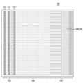
도 8은 균일한 광 추출을 위한 패턴(500)의 밀도 변화를 공간적으로 나타내는 그래프로서, 이와 같은 균일한 광 추출을 위한 밀도 보강부(501)가 필요한 부분을 나타내고 있다. 그래프의 X 방향은 도광판(200)의 입광부(210) 측을 나타내고 있고, Y 방향은 도광판(200)의 입광부(210)에서 단부(250) 측을 잇는 측면을 나타내고 있다.FIG. 8 is a graph showing a spatial change in the density of the
도 8에서 "A" 부분과 같이, 밀도(density)가 크게 나타나는 부분이 보다 밀도가 큰 패턴(500)이 필요한 부분이 될 수 있으며, "B" 부분은 패턴(500)의 밀도가 감소되는 것이 유리한 부분을 나타내고 있다. 즉, 패턴(500) 밀도가 증가되는 것이 유리한 부분은 출광면(220)의 밝기가 어두운 면을 나타내고, 밀도가 감소되는 것이 유리한 부분은 밝기가 밝은 면을 나타내고 있음을 알 수 있다.8, a portion having a larger density may be a portion where a more
여기서, Y 방향의 밀도를 그래프로 나타내면 도 9에서와 같다. 도 9에서 보면 입광부측에서 어두운 부분(즉, 밀도 증가가 필요한 부분)이 네 군데 나타나 있고, 입광부의 반대측에도 어두운 부분이 있음을 알 수 있다.Here, the density in the Y direction is represented by a graph as shown in FIG. It can be seen from FIG. 9 that there are four dark areas on the light incoming side (i.e., areas where density increase is required) and dark areas on the opposite side of the light entering area.
즉, 출광면(220)에서 균일한 광 추출을 위해서는 패턴(500) 밀도의 변화가 필요하며, 이는 (3)번 또는 (4)번의 특이점 중 하나를 무시한다면 세 군데, 이를 포함한다면 네 군데의 국지적인 밀도 증가가 적용되었을 경우에 균일성이 향상될 수 있음을 나타낸다.That is, in order to uniformly extract light from the
또한, 입광부의 반대측에는 패턴(500)의 밀도가 단부측으로 갈수록 점차로 증가한다면 출광면의 균일성이 보다 향상될 수 있음을 나타내고 있으며, 이러한 입 광부와 그 단부 사이의 중간 부분에서는 밀도가 대체적으로 균일함을 알 수 있다. The uniformity of the light emitting surface can be further improved if the density of the
따라서, 이러한 사항을 적용하면 도광판(200)의 패턴(500)의 일례는 도 10과 같이 형성될 수 있다.Accordingly, by applying such a matter, an example of the
즉, 광 추출 패턴(500)은, 입광부(210)에 가까운 부분에 국지적으로 패턴(500) 밀도가 증가하는 밴드형 밀도 보강부(521, 522, 523, 524)를 가지는 제 1패턴부(520)와, 입광부(210)가 위치하는 부분의 반대측에 위치한 단부(250)에 가까운 부분에 밀도가 단부(250)로 갈수록 점차 증가하는 제 2패턴부(530)를 가질 수 있다.That is, the
또한, 이러한 제 1패턴부(520)와 제 2패턴부(530) 사이에 위치하여 밀도가 실질적으로 동일하거나 거의 변화하지 않는 제 3패턴부(540)가 포함될 수 있다.The
여기서, 제 1패턴부(520)에 위치하는 밴드형 밀도 보강부(521, 522, 523, 524)의 각 부분은 도 9의 (1) 내지 (4)로 표현되어 있는 각 특이점의 위치와 동일하거나 근접함을 알 수 있다.Here, the respective portions of the band-shaped
도 11은 이와 같은 패턴(500)을 갖는 도광판(200)의 다른 예의 하면(240)을 나타내고 있으며, 세 부분의 밴드형 밀도 보강부(521, 522, 523)가 위치하는 제 1패턴부(520)와, 제 2패턴부(530), 및 제 3패턴부(540)를 포함하는 광 추출 패턴(500)을 나타내고 있다.11 shows another example of the
상술한 바와 같이, 이러한 패턴(500)은 도광판(200)의 상면인 출광면(220)에도 형성될 수 있음은 물론이다.As described above, it is needless to say that the
이와 같이, 도광판의 출광면에서 어두운 부분은 패턴 밀도를 상대적으로 증가시키고, 밝은 부분은 패턴 밀도를 상대적으로 감소시킨 광 추출 패턴의 적용에 의하여, 백라이트 유닛의 광 추출면은 빛의 균일성이 크게 향상될 수 있고, 이러한 균일성 향상은 도광부 또는 백라이트 유닛을 모듈화하여 구성하는 경우에 보다 극대화될 수 있다.As described above, by applying the light extracting pattern in which the pattern density is relatively increased in the dark portion on the light exit surface of the light guide plate and the pattern density is relatively decreased in the light portion, the light extraction surface of the backlight unit has a large light uniformity And such uniformity improvement can be maximized when the light guide unit or the backlight unit is configured by modularization.
도 12에서는 도광판(200)의 하면(240)의 단부(250)측에 제 1패턴부(520)와, 제 2패턴부(530), 및 제 3패턴부(540)를 포함하는 광 추출 패턴(500)을 적용한 도광판(200)에 의한 광 추출 상태를 나타내고 있다.12 illustrates a light extraction pattern including a
도시하는 바와 같이, 입광부측(도 12의 상측)의 광의 균일성이 상대적으로 크게 향상되었음을 알 수 있다.As shown in the figure, it can be seen that the uniformity of light at the light-incoming portion side (upper side in Fig. 12) is relatively improved.
도 13에서는 광 추출 패턴(500)의 단위 형상(510)이 구형인 경우를 도시하고 있으며, 이러한 구형 단위 패턴을 적용하는 경우, 단위 패턴의 직경(D)과 깊이(H)의 비율은 대략 0.3 내지 1로 설정되는 것이 유리하다. 즉, 구형 음각 패턴의 단위 형상(510)을 가지는 경우, 직경(D)이 깊이(H)보다 크거나 같은 형상을 적용할 수 있다.13 shows a case where the
또한, 패턴(500)의 각 단위 형상(510)은 도 13 내지 도 17과 같이 다양한 형상을 적용할 수 있다. 이러한 다양한 형상은 양각 또는 음각 형상이 모두 적용 가능하다.In addition, various shapes can be applied to each
도 14에서는 피라미드형 단위 형상(511)을 가지는 패턴을 나타내고 있고, 도 15에서는 콘형 단위 형상(512)이 적용된 경우를 나타내고 있다.Fig. 14 shows a pattern having a
또한, 도 16에서는 패턴이 실린더(원통)형 단위 형상(513)을 가지는 경우를 나타내고 있고, 도 17에서는 패턴이 프리즘형 단위 형상(514)를 가지는 경우를 나 타내고 있으며, 도 18에서는 타원체형 단위 형상(515)를 가지는 경우를 나타내고 있다. 또한, 이 외에 가시(bur) 형상(도시되지 않음)을 가지는 경우도 가능하다.16 shows a case where the pattern has a cylindrical (cylinder)
한편, 이러한 패턴(500)은 도 19와 같이, 밀도가 변화되는 경계점을 제외하고 등간격을 이루는 등간격 패턴(500)이 적용될 수 있고, 또한, 도 20과 같이, 일정한 조건 하에서 무작위 배치되는 세미랜덤 패턴(500)이 적용될 수도 있다. As shown in FIG. 19, the
이러한 세미랜덤 패턴(500)은 단위 형상이 서로 겹치지 않으며, 단위 형상 간의 평균 거리가 일정한 조건 하에서 무작위하게 배열되는 패턴을 의미한다.The
이때, 등간격 패턴의 주기 또는 세미랜덤 패턴의 평균 거리는 20㎛ 내지 3mm가 될 수 있고, 패턴의 단위 형상의 직경은 20 내지 100㎛가 될 수 있으며, 그 깊이는 50㎛ 미만인 것이 유리하다.At this time, the period of the regular interval pattern or the average distance of the semi-random pattern may be 20 탆 to 3 mm, the diameter of the unit shape of the pattern may be 20 to 100 탆, and the depth is advantageously less than 50 탆.
이러한 단위 패턴의 형상은 형상은 코어(Core)를 레이저로 가공하여 사출하여 형성할 수 있고, 압출, 레이저 직접 가공, 또는 인쇄의 방법을 통하여 형성하는 것도 가능하다. The shape of the unit pattern can be formed by injecting the core by laser processing, or it can be formed by extrusion, direct laser processing, or printing.
한편, 도 21은 상술한 도 8과 같은 균일한 광 추출을 위한 패턴(500)의 밀도 변화를 공간적으로 나타내는 그래프로서, 광 추출의 균일성을 향상시키기 위하여 그래프의 X 방향 중에서 도광판(200)의 입광부(210) 측("C" 부분)과, 이 입광부(210)의 반대측의 상측부("D" 부분)를 고려할 수 있다.Meanwhile, FIG. 21 is a graph that spatially shows the density variation of the
즉, 도광판(200)의 입광부(210) 측의 "C" 부분의 상측부의 양측 단부(예를 들어, 입광부(210)가 위치하는 부분에 대응하는 단부 및 입광부(210)가 위치한 부분의 반대측에 위치한 단부(250))는 휘선이 발생할 수 있는 부분으로서, 밀도를 감소시킴으로써 빛의 균일성을 향상시킬 수 있음을 나타내고 있다. 이러한 휘선이 발생할 수 있는 이유 중 하나는 입광부(210)측이 광원부(400)로부터 가깝고, 또한 도광판(200)은 반사판(300)의 테두리부(310)로부터 반사되는 빛이 상대적으로 집중될 수 있기 때문이다.That is, both ends of the upper portion of the "C" portion of the
따라서, 이를 위하여 도 22에서와 같이, 입광부(210)가 위치하는 부분에 대응하는 단부 및 입광부(210)가 위치한 부분의 반대측에 위치한 단부(250)에서 패턴 밀도가 5 내지 10% 감소시킴으로써 광 추출되는 빛의 일부 감소시키는 것이 빛의 균일성 향상에 도움을 줄 수 있다.22, by reducing the pattern density by 5 to 10% at the
또한, 이와 같이 밀도를 감소시키는 위치는 도 21의 그래프로부터, 입광부(210) 전체 폭에 대하여, 단부로부터 5 내지 20%의 위치하는 것이 유리하다.21, it is advantageous that the position for decreasing the density is located at 5 to 20% from the end with respect to the entire width of the light-
한편, 입광부(210)가 위치하는 부분의 반대측에 위치한 단부를 나타내는 도 21의 "D" 부분은 도 23에서와 같이, 어두운 부분이 나타날 수 있으며, 따라서 단부측에서 그 밀도가 증가하였다가 다시 원래의 밀도 정도로 감소함으로써 출광면의 빛의 균일성을 향상시킬 수 있음을 나타내고 있다.On the other hand, in the portion "D" in Fig. 21 showing the end located on the opposite side of the portion where the light-
이러한 어두운 부분이 발생할 수 있는 이유 중 하나는 광원부(400)로부터 거리가 상대적으로 멀어지기 때문이다.One of the reasons why such a dark portion may occur is that the distance from the
따라서, 이와 같이 밀도가 증가하였다가 다시 감소되는 정도는 입광부(210)가 위치한 부분의 반대측에 위치한 단부측의 측면에 패턴 밀도가 5 내지 10% 증가하고 중앙측의 밀도 정도로 다시 감소하는 것이 유리하다.Accordingly, it is preferable that the pattern density is increased by 5 to 10% at the side of the end portion located on the opposite side of the portion where the light-entering
또한, 이와 같이 밀도가 증가하였다가 감소되는 부분의 위치는 도 21의 그래프로부터, 입광부(210)가 위치한 부분의 반대측에 위치한 단부 전체 폭에 대하여, 단부로부터 5 내지 30%의 위치에서 설정할 수 있다.21, the position of the portion where the density is increased and decreased can be set at a position of 5 to 30% from the end with respect to the entire width of the end portion located on the opposite side of the portion where the
이와 같은 광 추출 패턴을 갖는 도광판(200)은, 도 24에서 도시하는 바와 같 이, 작은 크기로 모듈화하여 구성할 수 있고, 서로 이웃하여 광적으로 결합하여 연결하여 대면적의 백라이트 유닛을 구성하는 경우에 적용될 수 있으며, 이러한 모듈형 백라이트 유닛에서의 출광되는 광의 균일성을 크게 향상시킬 수 있다.As shown in Fig. 24, the
도 24에서는 네 개의 도광판 모듈(A, B, C, D)가 서로 이웃하여 결합된 상태를 도시하고 있으며, 광원부(400)는 각 모듈의 일변에 위치하는 것을 나타내고 있다.In FIG. 24, four light guide plate modules A, B, C and D are adjacently joined to one another, and the
이러한 배열에 의하여 출광면(220)은 서로 연결되어 구성되며, 상술한 각 모듈 간의 광적 결합에 의하여 각 모듈 사이의 연결부에 나타날 수 있는 휘암선발생이 개선될 수 있으며, 여기에 상술한 광 추출 패턴에 의하여 각 모듈에서 발생할 수 있는 휘암선의 발생도 개선될 수 있어, 백라이트 유닛의 전체적인 출광면(220)에서의 광 균일성이 크게 향상될 수 있는 것이다.According to the arrangement, the
상술한 본 발명의 실시예에서는 한변의 길이가 5인치인 도광판을 어레이하여 대화면 백라이트 유닛에 적용하는 경우의 예를 나타내고 있으며, 이러한 도광판의 크기 및 전체 백라이트 유닛의 크기는 적용하고자 하는 제품에 따라 다양하게 선택될 수 있음은 물론이다.In the embodiment of the present invention, a light guide plate having a length of 5 inches on one side is arrayed and applied to a large-screen backlight unit. The size of the light guide plate and the size of the whole backlight unit vary depending on the product Of course.
상기 실시예는 본 발명의 기술적 사상을 구체적으로 설명하기 위한 일례로서, 본 발명은 상기 실시예에 한정되지 않으며, 다양한 형태의 변형이 가능하고, 이러한 기술적 사상의 여러 실시 형태는 모두 본 발명의 보호범위에 속함은 당연하다.While the present invention has been described in connection with what is presently considered to be practical exemplary embodiments, it is to be understood that the invention is not limited to the disclosed embodiments, but, on the contrary, It is natural to belong to the scope.
도 1은 도광부 또는 도광판 모듈의 일례를 나타내는 사시도이다.1 is a perspective view showing an example of a light guide portion or a light guide plate module.
도 2는 도광부 또는 도광판 모듈의 측면도이다.2 is a side view of the light guide portion or the light guide panel module.
도 3은 패턴을 갖는 도광판의 일 실시예를 나타내는 단면도이다.3 is a cross-sectional view showing an embodiment of a light guide plate having a pattern.
도 4는 도 3의 패턴의 밀도를 나타내는 그래프이다.4 is a graph showing the density of the pattern of Fig.
도 5는 도 3의 패턴을 갖는 도광판의 일 실시예를 나타내는 배면도이다.Fig. 5 is a rear view showing an embodiment of a light guide plate having the pattern of Fig. 3;
도 6은 도 3의 패턴을 갖는 도광판에 의한 광 분포를 나타내는 시뮬레이션 도이다.Fig. 6 is a simulation diagram showing light distribution by the light guide plate having the pattern of Fig. 3;
도 7은 패턴 개수당 휘도값을 나타내는 그래프이다.7 is a graph showing a luminance value per pattern number.
도 8은 균일한 광 추출을 위한 패턴의 밀도 변화를 공간적으로 나타내는 그래프이다.FIG. 8 is a graph showing the density change of the pattern for uniform light extraction spatially.
도 9는 도 8의 Y 방향 패턴 곡선을 나타내는 그래프이다.9 is a graph showing a Y-direction pattern curve of FIG.
도 10은 패턴을 갖는 도광판의 다른 실시예를 나타내는 단면도이다.10 is a cross-sectional view showing another embodiment of a light guide plate having a pattern.
도 11은 패턴을 갖는 도광판의 다른 실시예를 나타내는 배면도이다.11 is a rear view showing another embodiment of a light guide plate having a pattern.
도 12는 도 10의 패턴을 갖는 도광판에 의한 광 분포를 나타내는 시뮬레이션 도이다.12 is a simulation view showing light distribution by the light guide plate having the pattern of Fig.
도 13은 단위 패턴의 형상 및 조건을 나타내는 개략도이다.13 is a schematic diagram showing the shape and condition of the unit pattern.
도 14 내지 도 18은 단위 패턴의 다양한 형상을 나타내는 개략도이다.14 to 18 are schematic views showing various shapes of unit patterns.
도 19는 등간격 패턴을 나타내는 개략도이다.19 is a schematic diagram showing an equally spaced pattern.
도 20은 세미랜덤 패턴을 나타내는 개략도이다.20 is a schematic view showing a semi-random pattern.
도 21은 균일한 광 추출을 위한 패턴의 밀도 변화를 공간적으로 나타내는 그래프이다.FIG. 21 is a graph showing the density change of the pattern for uniform light extraction spatially.
도 22는 도 21의 "C" 부분을 적용한 그래프이다.22 is a graph to which the portion "C" in Fig. 21 is applied.
도 23은 도 21의 "D" 부분을 적용한 그래프이다. 23 is a graph to which the portion "D" in Fig. 21 is applied.
도 24는 모듈형 백라이트 유닛의 일례를 나타내는 평면도이다.24 is a plan view showing an example of a modular backlight unit.
Claims (14)
Priority Applications (4)
| Application Number | Priority Date | Filing Date | Title |
|---|---|---|---|
| KR1020090048571A KR101565409B1 (en) | 2009-06-02 | 2009-06-02 | LED back-light unit |
| EP10783498.8A EP2438484A4 (en) | 2009-06-02 | 2010-01-12 | Led back-light unit and display device |
| PCT/KR2010/000180 WO2010140749A1 (en) | 2009-06-02 | 2010-01-12 | Led back-light unit and display device |
| US12/704,357 US8277104B2 (en) | 2009-06-02 | 2010-02-11 | LED back-light unit and display device |
Applications Claiming Priority (1)
| Application Number | Priority Date | Filing Date | Title |
|---|---|---|---|
| KR1020090048571A KR101565409B1 (en) | 2009-06-02 | 2009-06-02 | LED back-light unit |
Publications (2)
| Publication Number | Publication Date |
|---|---|
| KR20100129949A KR20100129949A (en) | 2010-12-10 |
| KR101565409B1 true KR101565409B1 (en) | 2015-11-03 |
Family
ID=43220017
Family Applications (1)
| Application Number | Title | Priority Date | Filing Date |
|---|---|---|---|
| KR1020090048571A Expired - Fee Related KR101565409B1 (en) | 2009-06-02 | 2009-06-02 | LED back-light unit |
Country Status (4)
| Country | Link |
|---|---|
| US (1) | US8277104B2 (en) |
| EP (1) | EP2438484A4 (en) |
| KR (1) | KR101565409B1 (en) |
| WO (1) | WO2010140749A1 (en) |
Families Citing this family (18)
| Publication number | Priority date | Publication date | Assignee | Title |
|---|---|---|---|---|
| WO2008126011A1 (en) * | 2007-04-12 | 2008-10-23 | Koninklijke Philips Electronics N.V. | Improved light guide and light-output device |
| KR20110114641A (en) * | 2009-02-23 | 2011-10-19 | 샤프 가부시키가이샤 | Illumination device, surface light source device, and liquid crystal display device |
| TW201222028A (en) * | 2010-11-23 | 2012-06-01 | Genius Electronic Optical Co Ltd | Light guide module |
| JP5751922B2 (en) * | 2011-05-09 | 2015-07-22 | キヤノン株式会社 | Light emitting device and display device |
| JP5821361B2 (en) * | 2011-07-25 | 2015-11-24 | セイコーエプソン株式会社 | LIGHTING DEVICE, LIQUID CRYSTAL DISPLAY DEVICE, AND ELECTRONIC DEVICE |
| JP5821539B2 (en) * | 2011-11-07 | 2015-11-24 | セイコーエプソン株式会社 | LIGHTING DEVICE, LIQUID CRYSTAL DISPLAY DEVICE, AND ELECTRONIC DEVICE |
| KR20130051135A (en) * | 2011-11-09 | 2013-05-20 | 삼성전자주식회사 | Backlight unit and display apparatus having the same |
| JP5952086B2 (en) * | 2012-05-24 | 2016-07-13 | スタンレー電気株式会社 | Vehicle lighting |
| JP5621015B1 (en) * | 2013-05-31 | 2014-11-05 | シャープ株式会社 | Light guide plate, illumination device, display device, and television receiver |
| US10371884B2 (en) * | 2014-08-04 | 2019-08-06 | Dolby Laboratories Licensing Corporation | Tiled assemblies for a high dynamic range display panel |
| US9684116B2 (en) * | 2014-08-18 | 2017-06-20 | New Optics, Ltd | Light guide plate, and backlight unit and display device including the same |
| CN104696887B (en) * | 2015-03-26 | 2018-06-15 | 合肥鑫晟光电科技有限公司 | A kind of light guide plate, backlight module, display device and display control program |
| KR102276416B1 (en) * | 2015-03-26 | 2021-07-14 | 삼성디스플레이 주식회사 | Display apparatus |
| JP6907002B2 (en) * | 2017-04-06 | 2021-07-21 | 株式会社小糸製作所 | Three-dimensional surface display device and vehicle display device |
| US10605980B2 (en) | 2017-06-04 | 2020-03-31 | Svv Technology Innovations, Inc. | Stepped light guide illumination systems |
| CN107561772B (en) * | 2017-08-15 | 2021-07-13 | 昆山龙腾光电股份有限公司 | Backlight module and display device |
| TWI686634B (en) * | 2019-07-11 | 2020-03-01 | 友達光電股份有限公司 | Display device |
| EP3795895A1 (en) * | 2019-09-20 | 2021-03-24 | ewo GmbH | Modular light extraction unit for producing uniform luminance |
Citations (3)
| Publication number | Priority date | Publication date | Assignee | Title |
|---|---|---|---|---|
| JP2006004915A (en) * | 2004-05-20 | 2006-01-05 | Seiko Instruments Inc | Illumination device and display device using the same |
| JP2006134748A (en) * | 2004-11-08 | 2006-05-25 | Mitsubishi Rayon Co Ltd | Tandem surface light source device |
| JP2009093808A (en) * | 2007-10-03 | 2009-04-30 | Sharp Corp | Illumination device and liquid crystal display device |
Family Cites Families (20)
| Publication number | Priority date | Publication date | Assignee | Title |
|---|---|---|---|---|
| JP3654410B2 (en) * | 1997-08-11 | 2005-06-02 | 株式会社エンプラス | Sidelight type surface light source device, liquid crystal display device, and light guide plate |
| JP2001184929A (en) * | 1999-12-24 | 2001-07-06 | Nec Corp | Plane light source apparatus and liquid crystal display provided with it |
| JP2002116440A (en) * | 2000-10-10 | 2002-04-19 | Sony Corp | Backlight mechanism of liquid crystal display |
| JP4049624B2 (en) * | 2001-07-27 | 2008-02-20 | 株式会社エンプラス | Surface light source device, image display device, and light guide plate |
| JP2004184493A (en) * | 2002-11-29 | 2004-07-02 | Seiko Epson Corp | Electro-optical device, method of manufacturing electro-optical device, and electronic apparatus |
| US7465083B2 (en) * | 2003-03-07 | 2008-12-16 | Enplas Corporation | Focusing plate, surface light source device, and image display device |
| DE10314525A1 (en) * | 2003-03-31 | 2004-11-04 | Osram Opto Semiconductors Gmbh | Method of manufacturing a lighting device and lighting device |
| DE102004046696A1 (en) * | 2004-05-24 | 2005-12-29 | Osram Opto Semiconductors Gmbh | Method for assembling a surface luminous system and surface luminous system |
| JP2006032020A (en) * | 2004-07-13 | 2006-02-02 | Sharp Corp | Liquid crystal display |
| US7311431B2 (en) * | 2005-04-01 | 2007-12-25 | Avago Technologies Ecbu Ip Pte Ltd | Light-emitting apparatus having a plurality of adjacent, overlapping light-guide plates |
| KR101167311B1 (en) * | 2005-06-29 | 2012-07-19 | 엘지디스플레이 주식회사 | Backlight unit for Field sequential Liquid Crystal Display device |
| KR100780205B1 (en) * | 2006-04-21 | 2007-11-27 | 삼성전기주식회사 | Backlight Unit for Liquid Crystal Display |
| JP4735849B2 (en) * | 2006-10-26 | 2011-07-27 | ミネベア株式会社 | Surface lighting device |
| JP2008192395A (en) * | 2007-02-02 | 2008-08-21 | Seiko Instruments Inc | Lighting device, and liquid crystal display device |
| US20080205078A1 (en) * | 2007-02-23 | 2008-08-28 | Luminus Devices, Inc. | Illumination tiles and related methods |
| US7961271B2 (en) * | 2007-02-27 | 2011-06-14 | Seiko Instruments Inc. | Lighting device and display device provided with the same |
| US8154689B2 (en) * | 2007-04-26 | 2012-04-10 | Sharp Kabushiki Kaisha | Light emitting element and liquid crystal display apparatus |
| JP5104770B2 (en) * | 2008-03-28 | 2012-12-19 | 豊田合成株式会社 | Backlight device |
| WO2009145548A2 (en) * | 2008-05-27 | 2009-12-03 | Lg Electronics Inc. | Led back-light unit and liquid crystal display device using the same |
| KR101676870B1 (en) * | 2009-07-31 | 2016-11-16 | 엘지전자 주식회사 | Backlight unit and display apparatus thereof |
-
2009
- 2009-06-02 KR KR1020090048571A patent/KR101565409B1/en not_active Expired - Fee Related
-
2010
- 2010-01-12 EP EP10783498.8A patent/EP2438484A4/en not_active Withdrawn
- 2010-01-12 WO PCT/KR2010/000180 patent/WO2010140749A1/en not_active Ceased
- 2010-02-11 US US12/704,357 patent/US8277104B2/en not_active Expired - Fee Related
Patent Citations (3)
| Publication number | Priority date | Publication date | Assignee | Title |
|---|---|---|---|---|
| JP2006004915A (en) * | 2004-05-20 | 2006-01-05 | Seiko Instruments Inc | Illumination device and display device using the same |
| JP2006134748A (en) * | 2004-11-08 | 2006-05-25 | Mitsubishi Rayon Co Ltd | Tandem surface light source device |
| JP2009093808A (en) * | 2007-10-03 | 2009-04-30 | Sharp Corp | Illumination device and liquid crystal display device |
Also Published As
| Publication number | Publication date |
|---|---|
| US20100302805A1 (en) | 2010-12-02 |
| EP2438484A4 (en) | 2015-05-20 |
| US8277104B2 (en) | 2012-10-02 |
| WO2010140749A1 (en) | 2010-12-09 |
| KR20100129949A (en) | 2010-12-10 |
| EP2438484A1 (en) | 2012-04-11 |
Similar Documents
| Publication | Publication Date | Title |
|---|---|---|
| KR101565409B1 (en) | LED back-light unit | |
| US7400817B2 (en) | Light guide member and backlight unit including light guide member and methods of fabricating light guide members and backlight units | |
| US7948579B2 (en) | Planar lighting device and liquid crystal display device using the same | |
| KR100978078B1 (en) | Prism sheet and liquid crystal display device having same | |
| JP4992721B2 (en) | Surface light emitting device and liquid crystal display device | |
| US20080062718A1 (en) | Light guide plate with high-density diffusing dots and backlight module using the same | |
| EP2378325B1 (en) | Image display apparatus and backlight apparatus used therefor | |
| CN101750665A (en) | Light guide plate and backlight module using same | |
| JP2009289701A (en) | Lighting device, plane light source device, and liquid crystal display | |
| JP2012018880A (en) | Planar lighting device, image display device, and optical sheet | |
| JP2011238484A (en) | Backlight device and liquid crystal display | |
| US20110019437A1 (en) | Light source module and display module | |
| JP5685099B2 (en) | Surface light source element and display device including the same | |
| JP5068865B2 (en) | Light source module and electronic device including the same | |
| KR100879948B1 (en) | Side Dimming Backlight Device Using Micro Rectangular Lens Pattern | |
| JP2004171870A (en) | Lighting system and liquid crystal display device | |
| TWI407162B (en) | Light guide plate and backlight module | |
| JP2006134661A (en) | Planar light source and liquid crystal display device using the same | |
| JP2015191686A (en) | Light guide, edge light type lighting apparatus and image display device | |
| JP4984512B2 (en) | Surface light emitting device and liquid crystal display device | |
| JP5458772B2 (en) | Depolarization sheet, backlight unit and display device | |
| TWI399590B (en) | Liquid crystal display, backlight module thereof and light guide structure thereof | |
| JP2007123086A (en) | Surface light source apparatus | |
| KR20080028684A (en) | Light guide plate, backlight unit and liquid crystal display device using the same | |
| TWI709774B (en) | Light guide plate and light source module |
Legal Events
| Date | Code | Title | Description |
|---|---|---|---|
| PA0109 | Patent application |
St.27 status event code: A-0-1-A10-A12-nap-PA0109 |
|
| R18-X000 | Changes to party contact information recorded |
St.27 status event code: A-3-3-R10-R18-oth-X000 |
|
| PG1501 | Laying open of application |
St.27 status event code: A-1-1-Q10-Q12-nap-PG1501 |
|
| A201 | Request for examination | ||
| P11-X000 | Amendment of application requested |
St.27 status event code: A-2-2-P10-P11-nap-X000 |
|
| P13-X000 | Application amended |
St.27 status event code: A-2-2-P10-P13-nap-X000 |
|
| PA0201 | Request for examination |
St.27 status event code: A-1-2-D10-D11-exm-PA0201 |
|
| R17-X000 | Change to representative recorded |
St.27 status event code: A-3-3-R10-R17-oth-X000 |
|
| PN2301 | Change of applicant |
St.27 status event code: A-3-3-R10-R13-asn-PN2301 St.27 status event code: A-3-3-R10-R11-asn-PN2301 |
|
| E902 | Notification of reason for refusal | ||
| PE0902 | Notice of grounds for rejection |
St.27 status event code: A-1-2-D10-D21-exm-PE0902 |
|
| E13-X000 | Pre-grant limitation requested |
St.27 status event code: A-2-3-E10-E13-lim-X000 |
|
| P11-X000 | Amendment of application requested |
St.27 status event code: A-2-2-P10-P11-nap-X000 |
|
| P13-X000 | Application amended |
St.27 status event code: A-2-2-P10-P13-nap-X000 |
|
| E701 | Decision to grant or registration of patent right | ||
| PE0701 | Decision of registration |
St.27 status event code: A-1-2-D10-D22-exm-PE0701 |
|
| GRNT | Written decision to grant | ||
| PR0701 | Registration of establishment |
St.27 status event code: A-2-4-F10-F11-exm-PR0701 |
|
| PR1002 | Payment of registration fee |
St.27 status event code: A-2-2-U10-U11-oth-PR1002 Fee payment year number: 1 |
|
| PG1601 | Publication of registration |
St.27 status event code: A-4-4-Q10-Q13-nap-PG1601 |
|
| FPAY | Annual fee payment |
Payment date: 20180921 Year of fee payment: 4 |
|
| PR1001 | Payment of annual fee |
St.27 status event code: A-4-4-U10-U11-oth-PR1001 Fee payment year number: 4 |
|
| FPAY | Annual fee payment |
Payment date: 20190924 Year of fee payment: 5 |
|
| PR1001 | Payment of annual fee |
St.27 status event code: A-4-4-U10-U11-oth-PR1001 Fee payment year number: 5 |
|
| PN2301 | Change of applicant |
St.27 status event code: A-5-5-R10-R13-asn-PN2301 St.27 status event code: A-5-5-R10-R11-asn-PN2301 |
|
| PR1001 | Payment of annual fee |
St.27 status event code: A-4-4-U10-U11-oth-PR1001 Fee payment year number: 6 |
|
| PR1001 | Payment of annual fee |
St.27 status event code: A-4-4-U10-U11-oth-PR1001 Fee payment year number: 7 |
|
| PC1903 | Unpaid annual fee |
St.27 status event code: A-4-4-U10-U13-oth-PC1903 Not in force date: 20221029 Payment event data comment text: Termination Category : DEFAULT_OF_REGISTRATION_FEE |
|
| PC1903 | Unpaid annual fee |
St.27 status event code: N-4-6-H10-H13-oth-PC1903 Ip right cessation event data comment text: Termination Category : DEFAULT_OF_REGISTRATION_FEE Not in force date: 20221029 |