KR101540455B1 - Contact sensing method and apparatus - Google Patents
Contact sensing method and apparatus Download PDFInfo
- Publication number
- KR101540455B1 KR101540455B1 KR1020090022431A KR20090022431A KR101540455B1 KR 101540455 B1 KR101540455 B1 KR 101540455B1 KR 1020090022431 A KR1020090022431 A KR 1020090022431A KR 20090022431 A KR20090022431 A KR 20090022431A KR 101540455 B1 KR101540455 B1 KR 101540455B1
- Authority
- KR
- South Korea
- Prior art keywords
- contact
- signal
- sensing
- noise
- representative value
- Prior art date
- Legal status (The legal status is an assumption and is not a legal conclusion. Google has not performed a legal analysis and makes no representation as to the accuracy of the status listed.)
- Expired - Fee Related
Links
Images


Classifications
-
- G—PHYSICS
- G06—COMPUTING OR CALCULATING; COUNTING
- G06F—ELECTRIC DIGITAL DATA PROCESSING
- G06F3/00—Input arrangements for transferring data to be processed into a form capable of being handled by the computer; Output arrangements for transferring data from processing unit to output unit, e.g. interface arrangements
- G06F3/01—Input arrangements or combined input and output arrangements for interaction between user and computer
- G06F3/03—Arrangements for converting the position or the displacement of a member into a coded form
- G06F3/041—Digitisers, e.g. for touch screens or touch pads, characterised by the transducing means
- G06F3/0416—Control or interface arrangements specially adapted for digitisers
- G06F3/0418—Control or interface arrangements specially adapted for digitisers for error correction or compensation, e.g. based on parallax, calibration or alignment
- G06F3/04182—Filtering of noise external to the device and not generated by digitiser components
-
- G—PHYSICS
- G06—COMPUTING OR CALCULATING; COUNTING
- G06F—ELECTRIC DIGITAL DATA PROCESSING
- G06F3/00—Input arrangements for transferring data to be processed into a form capable of being handled by the computer; Output arrangements for transferring data from processing unit to output unit, e.g. interface arrangements
- G06F3/01—Input arrangements or combined input and output arrangements for interaction between user and computer
- G06F3/03—Arrangements for converting the position or the displacement of a member into a coded form
- G06F3/033—Pointing devices displaced or positioned by the user, e.g. mice, trackballs, pens or joysticks; Accessories therefor
- G06F3/0354—Pointing devices displaced or positioned by the user, e.g. mice, trackballs, pens or joysticks; Accessories therefor with detection of 2D relative movements between the device, or an operating part thereof, and a plane or surface, e.g. 2D mice, trackballs, pens or pucks
- G06F3/03547—Touch pads, in which fingers can move on a surface
-
- G—PHYSICS
- G06—COMPUTING OR CALCULATING; COUNTING
- G06F—ELECTRIC DIGITAL DATA PROCESSING
- G06F3/00—Input arrangements for transferring data to be processed into a form capable of being handled by the computer; Output arrangements for transferring data from processing unit to output unit, e.g. interface arrangements
- G06F3/01—Input arrangements or combined input and output arrangements for interaction between user and computer
- G06F3/03—Arrangements for converting the position or the displacement of a member into a coded form
- G06F3/041—Digitisers, e.g. for touch screens or touch pads, characterised by the transducing means
- G06F3/044—Digitisers, e.g. for touch screens or touch pads, characterised by the transducing means by capacitive means
Landscapes
- Engineering & Computer Science (AREA)
- General Engineering & Computer Science (AREA)
- Theoretical Computer Science (AREA)
- Human Computer Interaction (AREA)
- Physics & Mathematics (AREA)
- General Physics & Mathematics (AREA)
- Position Input By Displaying (AREA)
Abstract
본 발명은 접촉 감지 방법 및 장치에 관한 것이다. 본 발명에 따른 접촉 감지 방법은 접촉에 의해 생성되는 감지 신호를 획득하는 단계, 상기 접촉 발생시 생성되는 잡음 신호의 대표값을 계산하는 단계, 및 상기 감지 신호 및 상기 잡음 신호의 대표값을 이용하여 상기 접촉을 판단하는 단계를 포함한다. 본 발명에 따르면, 접촉 감지 장치의 감지 전극에서 접촉에 의해 생성되는 감지 신호 및 잡음 신호를 이용하여 접촉을 판단함으로써, 잡음 신호의 영향을 제거하여 보다 정확하게 접촉 입력을 판단할 수 있다.The present invention relates to a contact sensing method and apparatus. The contact sensing method according to the present invention includes the steps of acquiring a sensing signal generated by a contact, calculating a representative value of a noise signal generated at the time of the contact generation, and calculating a representative value of the noise signal using the representative value of the sensing signal and the noise signal And determining a contact. According to the present invention, it is possible to more precisely determine the contact input by eliminating the influence of the noise signal by determining the contact using the sensing signal and the noise signal generated by the contact at the sensing electrode of the contact sensing device.
감지 신호, 잡음 신호, 대표값, 오프셋 Sense signal, noise signal, representative value, offset
Description
본 발명은 접촉 감지 방법 및 장치에 관한 것으로서, 잡음 신호의 영향을 제거하여 접촉을 정확하게 판단할 수 있는 방법에 관한 내용을 개시한다.The present invention relates to a contact detection method and apparatus, and discloses a method for accurately determining contact by eliminating the influence of a noise signal.
접촉 감지 패널은 동작 방식에 따라 저항막 방식, 정전용량 방식, 초음파 방식, 적외선 방식 등으로 구분할 수 있으며, 이 중에서 특히 정전용량 방식은 접촉 감지 패널의 두께가 얇고, 내구성이 높으며, 멀티 터치가 가능하다는 고유의 장점을 갖는다. The contact detection panel can be classified into resistance film type, capacitive type, ultrasonic type, and infrared type depending on the operation type. Of these, the capacitive type is thin in thickness of contact detection panel, has high durability, It has its own advantages.
일반적인 정전용량 방식 접촉 감지 패널(예: 터치스크린 패널)은, PET 등으로 이루어진 기재(base material)의 일면에 감지 전극이 형성된 필름 형태의 기판과 컨트롤러 IC(integrated circuit)가 실장된 회로기판을 ACF 등으로 접합하여 제조된다. 한편 이와 같이 만들어진 필름-회로기판 형태의 패널은 사용자의 접촉을 수용하는 투명 윈도우에 OCA 등의 접착층을 이용하여 부착되며 전자 기기의 디스플레이(예: 액정 디스플레이, 유기전계발광표시장치, 플라즈마 디스플레이 패널)에 탑재된다.In general, a capacitive touch sensing panel (e.g., a touch screen panel) includes a film substrate on which a sensing electrode is formed on one surface of a base material made of PET or the like, and a circuit board on which a controller IC (integrated circuit) And the like. On the other hand, the thus formed film-circuit board type panel is attached to a transparent window that receives a user's contact using an adhesive layer such as OCA and is used as a display of an electronic device (e.g., a liquid crystal display, an organic light emitting display, Respectively.
접촉 감지 패널은 투명 윈도우의 전면에 가해지는 접촉 입력에 의해 생성되 는 감지 신호로부터 접촉 입력을 판단한다. 그러나 접촉 입력과 함께 압력이 투명 윈도우에 가해지는 경우, 접촉 감지 패널이 압력에 의해 물리적으로 변형됨에 따라 잡음 신호가 생성될 수 있으며, 이와 같은 잡음 신호는 접촉 입력의 정확한 판단을 저해할 수 있다.The touch sensing panel determines the contact input from the sensing signal generated by the touch input applied to the front of the transparent window. However, when pressure is applied to the transparent window with the touch input, a noise signal may be generated as the touch sensing panel is physically deformed by pressure, and such a noise signal may hinder accurate determination of the touch input.
따라서 본 발명의 목적은, 접촉 입력에 의해 잡음 신호가 발생하는 경우, 잡음 신호의 대표값을 이용하여 감지 신호에서 잡음 신호의 영향을 제거함으로써, 접촉 판단의 정확도를 향상할 수 있는 접촉 감지 방법 및 장치를 제공함에 있다.SUMMARY OF THE INVENTION It is therefore an object of the present invention to provide a touch sensing method capable of improving accuracy of contact determination by removing the influence of a noise signal in a sensing signal by using a representative value of a noise signal when a noise signal is generated by a contact input, Device.
상기 목적을 달성하기 위해 본 발명에 따른 접촉 감지 방법은, 접촉에 의해 생성되는 감지 신호를 획득하는 단계, 상기 감지 신호의 적어도 일부로부터 상기 접촉에 의해 생성되는 잡음 신호의 대표값을 추출하는단계, 및 상기 잡음 신호의 대표값 및 상기 감지 신호에 기초하여 상기 접촉을 판단하는 단계를 포함한다.According to an aspect of the present invention, there is provided a touch sensing method including the steps of acquiring a sensing signal generated by a touch, extracting a representative value of a noise signal generated by the touch from at least a part of the sensing signal, And determining the contact based on the representative value of the noise signal and the sensing signal.
또한, 본 발명에 따른 접촉 감지 장치는, 하나 이상의 전극이 배치되는 패널, 및 상기 전극으로부터 접촉에 의한 감지 신호를 획득하여 상기 접촉을 판단하는 접촉 감지부를 포함하고, 상기 접촉 감지부는 잡음 신호가 발생하면 상기 잡음 신호의 대표값을 추출하고, 상기 잡음 신호의 대표값 및 상기 감지 신호에 기초하여 상기 접촉을 판단한다.According to another aspect of the present invention, there is provided a touch sensing apparatus including a panel on which at least one electrode is disposed, and a touch sensing unit for acquiring a sensed signal by contact from the electrode to determine the touch, Extracts a representative value of the noise signal, and determines the contact based on the representative value of the noise signal and the sensing signal.
본 발명에 따르면, 접촉 감지 장치에서 접촉을 판단함에 있어서, 잡음 신호의 영향을 배제하여 접촉을 판단할 수 있다. 따라서, 접촉에 수반되는 압력으로 인해 패널이 변형됨으로써 의도하지 않은 잡음 신호가 발생하는 경우에도, 접촉 입력을 정확하게 판단할 수 있다.According to the present invention, in determining the contact in the contact sensing device, it is possible to determine the contact by excluding the influence of the noise signal. Therefore, even when an unintended noise signal is generated due to the deformation of the panel due to the contact pressure, the contact input can be accurately determined.
이하, 본 발명의 바람직한 실시예를 도면을 참조하여 설명한다.Hereinafter, preferred embodiments of the present invention will be described with reference to the drawings.
도 1은 본 발명의 일실시예에 따른 접촉 감지 장치를 포함하는 전자 기기를 도시한 도이다. 도 1을 참조하면, 본 실시예에 따른 전자 기기(100)는 PDA(Personal Digitial Assistant), 이동통신 단말기, PMP(Portable Media Player), 휴대용 게임기기, 스마트 폰과 같은 휴대용 장치는 물론, 텔레비전, 데스크톱 컴퓨터, LCD 모니터, DVD 플레이어 등과 같은 가정용 장치를 모두 포함한다.1 is a view illustrating an electronic device including a touch sensing device according to an embodiment of the present invention. Referring to FIG. 1, the
본 실시예에 따른 전자 기기(100)는 표시부(110), 하우징(120), 및 입력부(130) 등을 포함한다. 표시부(110)는 액정 디스플레이(LCD), 플라즈마 디스플레이 패널(PDP), 유기전계발광표시장치(OLED) 등과 같은 평판 디스플레이일 수 있으며, 표시부(110)의 전면에 접촉 감지 장치가 부착된다. 접촉 감지 장치가 부착된 표시부(110)를 구비함으로써, 사용자는 표시부(110)가 표시하는 화면에 접촉 입력을 인가할 수 있어, 보다 직관적인 사용자 인터페이스를 제공할 수 있다.The
입력부(130)는 접촉 감지 장치에서 처리하기 곤란한 입력 명령 혹은 전자 기기(100)의 동작에 자주 사용되는 입력 명령을 수행하기 위한 키를 별도로 마련한 것으로서, 전자 기기(100)의 구성에 따라 선택적으로 구비될 수 있다. 한편, 입력부(130)를 없애고 모든 입력을 접촉 감지 장치에서 처리하도록 하는 것도 가능함은 물론이다.The
도 2는 본 발명의 일실시예에 따른 접촉 감지 장치의 패널 구조를 도시한 도이다. 본 실시예에 따른 접촉 감지 장치(200)는 기판(210), 기판(210)의 일면에 배 치되는 감지 전극(220), 배선(230), 및 본딩 패드(240) 등을 구비하는 패널과, 접촉 감지부(250), 및 회로 기판(260) 등을 포함한다. 이하, 본 실시예에서는 1층 구조의 감지 전극(220)을 포함하는 접촉 감지 장치(200)로 설명하나, 2개 이상의 층에 감지 전극(220)이 배치되는 구조의 접촉 감지 장치(200)에도 본 발명이 적용 가능함은 물론이다.2 is a diagram illustrating a panel structure of a touch sensing apparatus according to an embodiment of the present invention. The
기판(210)은 PET(Polyethylene Terephthalate), PC(Polycarbonate), PES(Polyether Sulfone), PI(Polyimide), PMMA(Polymethyl methaacrylate) 등의 재료를 포함하는 기재로서, 접촉 감지 장치(200)가 전자 기기의 디스플레이 전면에 배치되는 경우, 빛 투과율이 우수한 재료를 포함하는 것이 바람직하다. 기판(210)의 일면에는 감지 전극(220), 배선(230), 본딩 패드(240) 등이 배치되며, 기판(210)은 OCA 등의 접착 부재를 통해 접촉 입력을 수용하는 윈도우에 부착되거나, 또는 감지 전극(220), 배선(230) 등이 배치된 면과 반대되는 면을 통해 직접 접촉 입력을 수용할 수도 있다.The
감지 전극(220)은 전기 전도성을 갖는 물질로 형성되며, 접촉 입력이 발생함에 따라 그에 대응하는 감지 신호가 감지 전극(220)에서 생성된다. 본 실시예에서 감지 신호는 감지 전극(220)과 접촉 객체를 전도성 판으로 하고, 감지 전극(220)과 접촉 객체 사이에 배치되는 기판(210), 접착 물질, 또는 윈도우 등을 유전체로 하는 정전용량(capacitance) 변화일 수 있다. 접촉 입력에 의해 생성되는 정전용량 변화는 접촉 객체에 의해 감지 전극(220) 상에 형성되는 접촉 면적에 비례하므로, 정전용량 변화에 기초하여 접촉 위치 등을 판단할 수 있다.The
감지 전극(220)은 ITO(Indium Tin Oxide), IZO(Indium Zinc Oxide), ZnO(Zinc Oxide), 또는 탄소나노튜브 등과 같은 투명 전도성 물질을 포함하며, 접촉 감지부(250)가 접촉을 판단할 수 있도록 소정의 패턴을 갖는다. 도 2를 참조하면, 본 실시예에서는 감지 전극(220)이 직각삼각형 형상의 패턴을 가지는 것을 가정하나, 이 외에 다른 다양한 패턴을 가지는 것도 가능하다. 감지 전극(220)은 배선(230)을 통해 기판(210)의 일단에 형성되는 본딩 패드(240)와 전기적으로 연결된다. The
접촉 감지부(250)는 회로 기판(260)에 실장되며, 회로 기판(260)은 ACF, ACP 등의 전도성 접착재료를 통해 본딩 패드(240)와 연결된다. 각각의 본딩 패드(240)는 하나의 감지 전극(220) 및 접촉 감지부(250)의 센싱 채널에 개별적으로 연결되므로, 접촉 감지부(250)는 접촉에 의해 생성되는 감지 신호를 감지 전극(220)으로부터 개별적으로 획득할 수 있다.The
접촉 입력이 인가되면, 감지 전극(220)에서 감지 신호가 생성되며, 동시에 소정의 잡음 신호가 발생할 수 있다. 접촉 입력은 기판(210) 또는 윈도우에 대한 압력을 수반할 수 있으며, 상기 잡음 신호는 이와 같은 압력에 비례하여 증가한다. 접촉 입력과 함께 기판(210) 혹은 윈도우에 가해지는 압력이 증가하는 경우, 기판(210)이 변형됨에 따라 잡음 신호가 발생할 수 있다. 이하, 도 3을 참조하여 설명한다.When the touch input is applied, a sensing signal is generated at the
도 3은 본 발명의 일실시예에 따른 접촉 감지 장치의 단면을 도시한 도이다. 도 3을 참조하면, 접촉 감지 장치(300)가 디스플레이(400) 상에 배치되며, 접촉 입 력이 인가됨에 따라 접촉 감지 장치(300)가 변형된다. 압력이 가해지지 않은 경우를 나타낸 점선 형태와 비교하여 실선으로 나타낸 형태와 같이 접촉 감지 장치(300)가 변형되면, 접촉 영역이 형성되지 않은 감지 전극(220)에서도 상기 변형에 의한 감지 신호, 즉 잡음 신호가 발생함으로써, 접촉 위치를 정확하게 판단할 수 없다. 이는 통상적으로, 접촉 감지부(250)가 계산하는 접촉 위치가 실제 접촉이 발생한 위치보다 기판(210)의 가운데 영역으로 치우치는 것으로 나타난다. 따라서, 잡음 신호의 영향을 고려하여 감지 신호를 수정하여 접촉을 판단하거나, 또는 잡음 신호의 영향을 반영하여 접촉 위치를 보정하는 것이 필요하다.3 is a cross-sectional view of a touch sensing apparatus according to an embodiment of the present invention. Referring to FIG. 3, the
도 4 및 도 5는 본 발명의 일실시예에 따른 접촉 감지 방법을 설명하기 위한 흐름도이다. 도 4를 참조하면, 본 발명의 제1실시예에 따른 접촉 감지 방법은 접촉 감지부(250)가 감지 전극(220)으로부터 감지 신호를 획득하는 것으로 시작한다(S40). 앞서 언급한 바와 같이 감지 신호는 접촉에 의해 감지 전극(220)에서 생성되는 정전용량 변화일 수 있으며, 접촉 감지부(250)는 각 센싱 채널에 개별적으로 연결된 감지 전극(220)으로부터 감지 신호를 획득한다.4 and 5 are flowcharts for explaining a touch sensing method according to an embodiment of the present invention. Referring to FIG. 4, the touch sensing method according to the first embodiment of the present invention starts with the
감지 신호를 획득하면, 접촉 감지부(250)는 잡음 신호가 발생하였는지 여부를 판단한다(S41). 접촉 영역은 사람의 손가락이 윈도우 또는 기판(210)에 닿으면서 형성되는 원으로 모델링될 수 있으며, 도 2에 도시한 바와 같은 감지 전극(220) 패턴을 가정하면, 접촉 영역은 통상적으로 3개 이하의 감지 전극(220)에서 형성된다. 따라서, 접촉 감지부(250)는 접촉 영역이 직접 형성되지 않은 감지 전극(220)에서 감지 신호를 획득하는 경우, 접촉 입력에 의한 패널의 변형에 따라 잡음 신호 가 발생한 것으로 판단 가능하다. 잡음 신호 발생 여부를 판단하는 방법에 관해서는 도 6 내지 도 8을 참고하여 설명한다.Upon acquiring the sensing signal, the
도 6에 도시한 바와 같이, 접촉 영역 A가 감지 전극 L2, L3, 및 R3에 형성된 경우를 가정하면, 도 7에 도시한 바와 같은 감지 신호 분포를 얻을 수 있다. 접촉 영역이 상대적으로 넓게 형성된 감지 전극 L2에서 가장 강한 감지 신호가 생성되며, 감지 전극 L3와 R3에서는 비슷한 크기의 감지 신호가 생성된다.Assuming that the contact region A is formed on the sensing electrodes L2, L3, and R3 as shown in Fig. 6, the sensing signal distribution as shown in Fig. 7 can be obtained. A strongest sensing signal is generated at the sensing electrode L2 having a relatively large contact region and a sensing signal having a similar magnitude is generated at the sensing electrodes L3 and R3.
한편, 도 7을 참조하면, 접촉 영역이 직접 형성되지 않은 감지 전극 L1, L4, L5, R1, R2, R5 등에서도 감지 신호가 생성된 것을 확인할 수 있다. 앞서 설명한 바와 같이 감지 신호는 감지 전극(220)과 접촉 객체를 전도성 판으로 하고, 접촉을 수용한 윈도우 및 OCA 접착 부재 등을 유전체로 하는 정전용량 변화이므로, 직접 접촉이 인가되지 않은 감지 전극에서도 감지 신호가 생성될 수 있다. 이러한 감지 신호는 접촉 영역에 가깝게 위치한 감지 전극(220)일수록 크게 나타므로, 본 실시예에서는 감지 전극 R2, R4, 및 L1, L3에서 특히 두드러지게 나타난다.Referring to FIG. 7, it can be seen that sensing signals are also generated in the sensing electrodes L1, L4, L5, R1, R2, and R5 where the contact region is not directly formed. As described above, since the sensing signal is a capacitance change in which the contact object with the
도 8은 접촉 영역 A에 접촉과 동시에 기판(210)이 물리적으로 변형될 수 있을 정도의 압력이 인가되어 감지 신호에 잡음 신호가 더해진 신호 분포도이다. 도 8을 참조하면, 도 7과 동일한 감지 신호 분포에 잡음 신호가 더해진다. 잡음 신호는 기판(210)의 변형 정도와 비례하여 나타나므로, 접촉 영역 A가 직접 형성되거나 접촉 영역 A와 인접한 감지 전극 L1~L5 및 R1~R5에서 크게 나타난다. 한편, 잡음 신호는 기판(210)이 변형되지 않은 경우에 감지 신호가 생성되지 않는 감지 전극 L6~L8 및 R6~R8에서도 생성되어 접촉 감지부(250)로 전달된다.8 is a signal distribution diagram in which a noise is added to a sensing signal when a pressure is applied to the
접촉이 인가되어 각 감지 전극(220)으로부터 감지 신호를 획득하면, 접촉 감지부(250)는 감지 신호의 분포에 기초하여 잡음 신호의 발생 여부를 판단할 수 있다. 즉, 감지 신호가 크게 나타나는 일정 개수의 감지 전극(본 실시예에서는 L1, L2, L3, R2, R3, R4)을 판단하고, 해당 감지 전극으로부터 이격되어 패널(210)의 변형이 없는 경우에 감지 신호가 생성되지 않거나 매우 작은 감지 신호가 나타나는 센싱 채널(본 실시예에서 L4~L8, R1, R5~R8)에서 감지 신호가 소정의 임계치보다 크게 나타나는 경우, 접촉 감지부(250)는 잡음 신호가 생성된 것으로 판단할 수 있다.When the contact is applied and a sensing signal is obtained from each
각 센싱 채널별로 획득한 감지 신호의 분포를 이용하여 잡음 신호가 생성된 것으로 판단하면, 접촉 감지부(250)는 잡음 신호의 대표값을 추출한다(S42). 잡음 신호의 대표값은, 접촉 판단의 기초가 되는 감지 신호에 포함된 잡음 신호를 보정하기 위한 값이며, 실제 접촉 판단 과정에서 감지 신호와 잡음 신호는 모두 동일한 정전용량 변화량으로 표현되므로, 잡음 신호의 대표값을 별도로 계산하여 감지 신호에서 잡음 신호의 영향을 제거하는 것이 바람직하다.If it is determined that the noise signal is generated using the distribution of the sensing signals acquired for each sensing channel, the
일실시예로, 접촉 감지부(250)는 소정 임계치 이하의 감지 신호의 합을 잡음 신호의 대표값으로 계산할 수 있다. 도 8에 도시한 감지 신호 분포도를 참조하면, 접촉 영역 A가 직접 형성되거나 접촉 영역이 가깝게 위치하여 상대적으로 강한 감지 신호를 획득할 수 있는 감지 전극 L1, L2, L3, 및 R2, R3, R4를 제외한 나머지 감지 전극에서 획득한 신호를 모두 합하여 잡음 신호의 대표값으로 계산한다. 즉, 소정 임계치 이하의 감지 신호의 합을 잡음 신호의 대표값으로 계산할 수도 있다. In one embodiment, the
접촉과 함께 기판(210)에 가해지는 압력에 의한 기판(210)의 변형으로 인해 나타나는 잡음 신호는, 큰 압력이 가해져 기판(210)의 변형 정도가 커질수록 크게 나타난다. 따라서, 접촉 영역이 직접 형성되지 않은 감지 전극에서 획득한 감지 신호, 또는 소정 임계치 이하의 감지 신호의 합을 잡음 신호의 대표값으로 적용할 수 있다. 이하, 설명의 편의를 위하여 잡음 신호의 대표값을 SideSum으로 표현하면, SideSum은 기판(210)에 가해지는 압력 및 접촉 위치에 영향을 받는다. 일례로, 기판(210)의 중앙 영역이 눌리면, 가장자리 영역에 동일한 압력이 가해진 경우보다 기판(210)의 변형이 크게 나타나므로, SideSum이 크게 나타날 수 있다.The noise signal due to the deformation of the
잡음 신호의 대표값 SideSum이 계산되면, 접촉 감지부(250)는 SideSum으로부터 잡음 보정량을 계산하고(S43), 계산한 잡음 보정량을 적용하여 감지 신호를 보정한다(S44). 이는 아래와 같은 식으로 표현될 수 있다.When the representative value SideSum of the noise signal is calculated, the
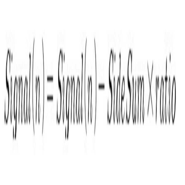
수학식 1에서 Signal(n)은 센싱 채널 n에 대응하는 감지 신호를 나타내며, 접촉에 의한 감지 신호 및 접촉에 따른 기판(210)의 변형에 의한 잡음 신호가 모두 포함된 값이다. 접촉 위치 계산에 필요한 센싱 채널 n의 감지 신호 Signal(n)에서 잡음 보정량에 해당하는 SideSum×ratio 값을 뺌으로써 잡음 신호의 영향을 제거할 수 있다.In Equation (1), Signal (n) represents a sensing signal corresponding to the sensing channel n, and includes a sensing signal due to contact and a noise signal due to deformation of the
ratio는 잡음 신호의 대표값 SideSum으로부터 잡음 보정량을 계산하기 위한 변수로서, 접촉이 인가된 위치 또는 잡음 신호의 대표값 SideSum 중 적어도 하나에 의존하는 값이거나, 미리 정해진 상수(constant)일 수 있다. SideSum에 ratio를 곱한 잡음 보정량을 접촉 영역이 형성된 전극과 연결된 채널의 감지 신호에서 뺌으로써, 접촉이 직접 발생한 감지 전극(220)에서 잡음 신호의 영향을 제외한 접촉 감지 신호만을 획득할 수 있다.The ratio is a parameter for calculating the noise correction amount from the representative value SideSum of the noise signal and may be a value depending on at least one of the position where the contact is applied or the representative value SideSum of the noise signal or may be a predetermined constant. The noise correction amount obtained by multiplying the SideSum by the ratio is subtracted from the sensing signal of the channel connected to the electrode in which the contact region is formed so that only the touch sensing signal except the influence of the noise signal can be obtained in the
잡음 보정량 SideSum×ratio는 접촉 위치에 따라 달라질 수 있다. 접촉이 기판(210)의 가운데 영역에 인가되면, 기판(210)의 가장자리 영역에 인가되는 경우보다 기판(210)의 변형이 크게 나타나므로, 잡음 신호 및 그에 따른 접촉 위치의 왜곡이 크게 나타난다. 따라서, 접촉이 기판(210)의 가운데 영역에서 발생하면, 기판(210)의 가장자리 영역에서 접촉이 발생하는 경우보다 잡음 보정량을 크게 적용하여 접촉 판단의 정확도를 높일 수 있다. 상기 언급한 바와 같이, 접촉이 인가된 위치에 의존하는 변수 ratio를 이용하여 잡음 보정량을 계산함으로써, 접촉 위치에 따른 잡음 보정량의 차등 적용이 가능할 것이다.The noise correction amount SideSum × ratio can be changed depending on the contact position. When the contact is applied to the center region of the
도 6에 도시한 전극 패턴을 갖는 패널에서, 가로 방향(X축 방향) 좌표는 좌측의 센싱 채널 L1~L8에서 획득하는 감지 신호의 합과, 우측의 센싱 채널 R1~R8에서 획득하는 감지 신호의 합의 비율을 이용하여 추출할 수 있다. 따라서, 센싱 채널 L4~L8(R1, R5~R8)에서 획득한 감지 신호의 합을 SideSum으로 추출하고 소정의 ratio를 반영하여 잡음 보정량을 계산한 후, 센싱 채널 L1~L3(R2~R4)에서 각각 획득한 감지 신호의 합에서 잡음 보정량을 제거하고, 센싱 채널 L1~L3의 감지 신호의 합과 R2~R4의 감지 신호의 합의 비율로부터 가로 방향 좌표를 추출함으로써, 잡음 신호의 영향을 제거할 수 있다. In the panel having the electrode pattern shown in Fig. 6, the horizontal direction (X-axis direction) coordinates correspond to the sum of the sensing signals obtained in the left sensing channels L1 to L8 and the sum of the sensing signals acquired in the right sensing channels R1 to R8 Can be extracted using the agreement ratio. Therefore, the sum of the sensing signals obtained from the sensing channels L4 to L8 (R1, R5 to R8) is extracted by SideSum, the noise correction amount is calculated by reflecting the predetermined ratio, and then the sensing channels L1 to L3 (R2 to R4) The influence of the noise signal can be removed by removing the noise correction amount from the sum of the obtained sensing signals and extracting the horizontal direction coordinates from the sum of the sensing signals of the sensing channels L1 to L3 and the sum of the sensing signals of R2 to R4 have.
잡음 신호의 영향이 제거된 접촉 감지 신호를 획득하면, 접촉 감지부(250)는 접촉 감지 신호에 기초하여 접촉 위치를 판단한다. 도 6에 도시한 접촉 영역 A의 경우, 센싱 채널 L1~L3, 및 R2~R4에서 획득한 감지 신호를 이용하여 접촉 위치를 판단할 수 있다. Upon acquiring the contact detection signal from which the influence of the noise signal is removed, the
한편, 수학식 1에 따른 잡음 신호 제거 과정을 여러 번 반복함으로써, 접촉 위치 판단의 정확도를 높일 수 있다. 일실시예로, 수학식 1에 의해 감지 신호에서 잡음 신호를 1차적으로 제거한 이후, 잡음 신호가 1차로 제거된 감지 신호를 바탕으로 산출한 접촉 위치를 반영하여 변수 ratio를 다시 설정한다. 상기와 같이 피드백(feedback) 단계를 적용하여 재설정된 ratio 값을 다시 수학식 1에 대입하여 접촉 위치를 산출함으로써, 잡음 신호에 따른 접촉 위치의 오차를 효율적으로 줄일 수 있다.On the other hand, by repeating the noise signal removing process according to Equation (1) several times, it is possible to improve accuracy of contact position determination. In one embodiment, after the noise signal is primarily removed from the sensing signal by Equation (1), the variable ratio is set again by reflecting the contact position calculated based on the sensing signal in which the noise signal is removed first. As described above, by applying the reset ratio value to the equation (1) by applying the feedback step as described above, it is possible to efficiently reduce the error of the contact position according to the noise signal.
도 5는 본 발명의 제2실시예에 따른 접촉 감지 방법을 설명하기 위한 흐름도이다. 도 4의 경우와 마찬가지로, 본 실시예에 따른 접촉 감지 방법 역시 접촉 감지부(250)가 감지 전극 L1~L8, R1~R8 각각으로부터 감지 신호를 획득하는 것으로 시작한다(S50). 본 실시예에서는 제1실시예와는 달리, S50 단계에서 획득한 감지 신호에 기초하여 접촉 위치를 바로 판단한다(S51). 이때, S51 단계에서는 추후 단계에서 산출되는 접촉 위치의 오차를 반영하여 보정 가능하도록 접촉 위치를 잠정 판단한다.5 is a flowchart illustrating a touch sensing method according to a second embodiment of the present invention. As in the case of FIG. 4, the touch sensing method according to the present embodiment also starts with the
접촉 입력과 함께 기판(210)에 가해진 압력에 의해 기판(210)이 변형되는 경 우, 접촉 감지부(250)가 판단한 접촉 위치는 실제 접촉 위치보다 기판(210)의 가운데 방향으로 왜곡되어 나타난다. 이는, 압력에 의해 기판(210)의 가운데 부분이 휘어짐으로써 각 센싱 채널에서 잡음 신호가 나타나기 때문이며, 본 실시예에서는 S51 단계에서 판단한 접촉 위치 자체를 보정하여 접촉 판단의 정확성을 높인다.When the
접촉 위치를 판단한 접촉 감지부(250)는 각 채널별로 획득한 감지 신호 분포에 기초하여 잡음 신호 발생 여부를 판단한다(S52). 잡음 신호 발생 여부를 판단하는 과정은, 앞서 설명한 S41 단계와 동일한 방법을 적용할 수 있다. S52 단계의 판단 결과 잡음 신호가 생성된 것으로 판단하면, 접촉 감지부(250)는 접촉 감지부(250)는 잡음 신호의 대표값을 추출하고(S53), 잡음 신호의 대표값으로부터 접촉 위치의 오차를 추정한 후(S54), 접촉 위치의 오차를 적용하여 S51 단계에서 잠정 판단한 접촉 위치를 보정함으로써 잡음 신호의 영향을 제거한다(S55). 접촉 위치의 왜곡을 수정하는 S53~S55 단계에서, S53 단계는 S42 단계에 대응한다. 이하, S54 및 S55 단계에 대해 도 9를 참조하여 보다 자세히 설명한다.The
도 9를 참조하면, 잡음 신호의 대표값을 가로축, 접촉 위치를 세로축으로 한 그래프가 표현된다. 잡음 신호의 대표값이 0일 때의 접촉 위치는 기판(210)에 가해진 압력에 따른 잡음 신호에 의한 접촉의 왜곡이 거의 없는 경우로서, 별도의 수정/보정 단계가 필요없다. 도 9에서 각각의 그래프 (1)~(6)은 서로 다른 위치에 가해진 접촉을 나타낸다. 세로축의 접촉 위치는, 접촉의 Y 좌표를 나타내는 것으로 가정하면, 각 그래프(1)~(6)은 다음과 같이 근사하여 표현할 수 있다.Referring to FIG. 9, a graph in which a representative value of a noise signal is represented by a horizontal axis and a contact position is represented by a vertical axis is represented. The contact position when the representative value of the noise signal is 0 is a case where there is almost no distortion of the contact due to the noise signal according to the pressure applied to the
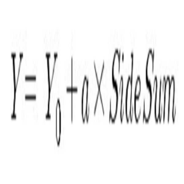
수학식 2에서 Y는 접촉의 Y좌표를 나타내며, SideSum은 가로축의 잡음 신호 대표값, Y0는 Y 절편으로서 잡음 신호 대표값이 0일 때의 접촉의 Y좌표, 즉, 압력에 따른 왜곡 등으로 인한 잡음 신호가 없는 이상적인 경우의 접촉의 Y좌표를 뜻한다. a는 비례 상수로서, 정해진 상수이거나 혹은 실제 접촉 위치 Y0에 의존하는 값일 수 있다. 동일한 압력이 기판(210)에 가해진다면, 기판(210)의 가운데 영역에 압력이 가해지는 경우가 기판(210)의 가장자리 영역에 압력이 가해지는 경우보다 더 많은 왜곡을 가져온다. 따라서, 도 9에 나타난 그래프 (1)~(6)에서 접촉 위치가 가운데 영역에 위치할수록 동일한 잡음 신호 기대 값에 대한 왜곡의 정도가 커지므로, 비례 상수 a는 Y0에 의존하는 값이 될 수 있다.In equation (2) with Y represents the Y coordinate of the contact, SideSum is Y coordinate of the contact when the horizontal axis of the noise signal representative value, Y 0 is the noise signal representative value as the Y-intercept is 0, that is, distortion due to pressure Means the Y-coordinate of the contact in the ideal case without any noise signal due to it. a is a constant, which may be a constant or a value depending on the actual contact position Y 0 . If the same pressure is applied to the
접촉 감지부(250)는 S53 단계에서 계산한 잡음 신호의 대표값에 소정의 비례치, 즉 수학식 2의 a 값을 반영하고, 접촉 위치에서 잡음 신호의 영향을 제거함으로써, 압력에 의한 왜곡이 보정된 좌표를 얻을 수 있다. 즉, 잡음 신호가 제거되지 않은 상태의 좌표 Y에서 잡음 신호의 대표값 SideSum에 비례치 a가 반영된 접촉 위치의 오차 a*SideSum을 뺌으로써, 압력에 의한 왜곡이 보정된 좌표 Y0를 얻을 수 있다(S54~S55).The
이상 본 발명의 바람직한 실시예에 대하여 도시하고 설명하였지만, 본 발명 은 상술한 특정의 실시예에 한정되지 아니하며, 청구범위에서 청구하는 본 발명의 요지를 벗어남이 없이 당해 발명이 속하는 기술분야에서 통상의 지식을 가진 자에 의해 다양한 변형실시가 가능하다. 또한, 첨부한 도면으로부터 용이하게 유추할 수 있는 사항은 상세한 설명에 기재되어 있지 않더라도 본 발명의 내용에 포함되는 것으로 보아야 할 것이며, 다양한 변형실시들은 본 발명의 기술적 사상이나 전망으로부터 개별적으로 이해되어져서는 안 될 것이다.While the present invention has been particularly shown and described with reference to exemplary embodiments thereof, it is to be understood that the invention is not limited to the disclosed exemplary embodiments, but, on the contrary, Various modifications can be made by those skilled in the art. It will be apparent to those skilled in the art that various modifications and variations can be made in the present invention without departing from the spirit or scope of the invention. It will not.
도 1은 본 발명에 따른 접촉 감지 장치를 포함하는 전자 기기를 도시한 도,1 is a view illustrating an electronic device including a touch sensing device according to the present invention.
도 2는 본 발명에 따른 접촉 감지 장치의 패널 구조를 도시한 평면도,2 is a plan view showing a panel structure of the touch sensing device according to the present invention,
도 4 및 도 5는 본 발명에 따른 접촉 감지 방법을 설명하기 위한 흐름도,4 and 5 are flowcharts for explaining a touch sensing method according to the present invention,
도 6 내지 도 8은 본 발명의 제1실시예에 따른 접촉 감지 방법을 설명하기 위한 도,6 to 8 are diagrams for explaining a touch sensing method according to the first embodiment of the present invention,
도 9는 본 발명의 제2실시예에 따른 접촉 감지 방법을 설명하기 위한 그래프이다.9 is a graph for explaining a touch sensing method according to the second embodiment of the present invention.
* 도면의 주요 부분에 대한 자세한 설명 ** Detailed description of main parts of drawing *
100 : 전자 기기 200 : 접촉 감지 장치100: Electronic device 200: Contact sensing device
210 : 기판 220 : 감지 전극210: substrate 220: sensing electrode
230 : 배선 250 : 접촉 감지부 230: Wiring 250: Contact sensing part
Claims (13)
Priority Applications (1)
| Application Number | Priority Date | Filing Date | Title |
|---|---|---|---|
| KR1020090022431A KR101540455B1 (en) | 2009-03-17 | 2009-03-17 | Contact sensing method and apparatus |
Applications Claiming Priority (1)
| Application Number | Priority Date | Filing Date | Title |
|---|---|---|---|
| KR1020090022431A KR101540455B1 (en) | 2009-03-17 | 2009-03-17 | Contact sensing method and apparatus |
Publications (2)
| Publication Number | Publication Date |
|---|---|
| KR20100104187A KR20100104187A (en) | 2010-09-29 |
| KR101540455B1 true KR101540455B1 (en) | 2015-07-30 |
Family
ID=43008462
Family Applications (1)
| Application Number | Title | Priority Date | Filing Date |
|---|---|---|---|
| KR1020090022431A Expired - Fee Related KR101540455B1 (en) | 2009-03-17 | 2009-03-17 | Contact sensing method and apparatus |
Country Status (1)
| Country | Link |
|---|---|
| KR (1) | KR101540455B1 (en) |
Citations (2)
| Publication number | Priority date | Publication date | Assignee | Title |
|---|---|---|---|---|
| KR20040106561A (en) * | 2002-05-17 | 2004-12-17 | 쓰리엠 이노베이티브 프로퍼티즈 컴파니 | Correction of memory effect errors in force-based touch panel systems |
| KR20040111634A (en) * | 2002-05-17 | 2004-12-31 | 쓰리엠 이노베이티브 프로퍼티즈 컴파니 | Calibration of force based touch panel systems |
-
2009
- 2009-03-17 KR KR1020090022431A patent/KR101540455B1/en not_active Expired - Fee Related
Patent Citations (2)
| Publication number | Priority date | Publication date | Assignee | Title |
|---|---|---|---|---|
| KR20040106561A (en) * | 2002-05-17 | 2004-12-17 | 쓰리엠 이노베이티브 프로퍼티즈 컴파니 | Correction of memory effect errors in force-based touch panel systems |
| KR20040111634A (en) * | 2002-05-17 | 2004-12-31 | 쓰리엠 이노베이티브 프로퍼티즈 컴파니 | Calibration of force based touch panel systems |
Also Published As
| Publication number | Publication date |
|---|---|
| KR20100104187A (en) | 2010-09-29 |
Similar Documents
| Publication | Publication Date | Title |
|---|---|---|
| JP3185748U (en) | Device for calibrating the effect of pressure on a touch sensor panel | |
| US8125464B2 (en) | Full scale calibration measurement for multi-touch surfaces | |
| KR101080181B1 (en) | Touch sensing panel and touch sensing apparatus including bilaterally adjacent electrodes | |
| US8570301B2 (en) | Negative pixel compensation | |
| CN103329074B (en) | Systems and methods for determining object information using estimated deflection responses | |
| KR101077854B1 (en) | Method and apparatus for sensing multiple touch-inputs | |
| TWI575414B (en) | Mode distinguishing method, touch-point locating method and touch control circuit | |
| JP6402884B2 (en) | Touch sensor device, electronic device, position calculation method, and position calculation program | |
| US20080100586A1 (en) | Method and system for calibrating a touch screen | |
| KR101749378B1 (en) | System and method for determining object information using an estimated rigid motion response | |
| KR101523379B1 (en) | Method of correcting position of touched point on touch-screen | |
| CN105320383A (en) | Adjustment of touch sensing stimulation voltage levels based on touch performance | |
| US8717325B1 (en) | Detecting presence of an object in the vicinity of a touch interface of a device | |
| EP2494431A1 (en) | Detection of gesture orientation on repositionable touch surface | |
| KR20120139518A (en) | Hybrid touch panel for sensing capacitance and pressure | |
| CN104142769A (en) | Method, medium and device for Restructuring Distorted Capacitive Touch Data | |
| KR20120033480A (en) | Touch screen | |
| CN103970357B (en) | Electronic device and touch point judgment method | |
| CN107239173B (en) | Touch device, touch display device and driving method thereof | |
| US10627951B2 (en) | Touch-pressure sensitivity correction method and computer-readable recording medium | |
| KR101540455B1 (en) | Contact sensing method and apparatus | |
| US20110199328A1 (en) | Touch screen system with acoustic and capacitive sensing | |
| KR20160022583A (en) | Touchscreen apparatus and method for sensing touch input | |
| JP2025187524A (en) | Electronic device and touch detection method |
Legal Events
| Date | Code | Title | Description |
|---|---|---|---|
| PA0109 | Patent application |
St.27 status event code: A-0-1-A10-A12-nap-PA0109 |
|
| PN2301 | Change of applicant |
St.27 status event code: A-3-3-R10-R11-asn-PN2301 St.27 status event code: A-3-3-R10-R13-asn-PN2301 |
|
| PG1501 | Laying open of application |
St.27 status event code: A-1-1-Q10-Q12-nap-PG1501 |
|
| PN2301 | Change of applicant |
St.27 status event code: A-3-3-R10-R11-asn-PN2301 St.27 status event code: A-3-3-R10-R13-asn-PN2301 |
|
| R18-X000 | Changes to party contact information recorded |
St.27 status event code: A-3-3-R10-R18-oth-X000 |
|
| R18-X000 | Changes to party contact information recorded |
St.27 status event code: A-3-3-R10-R18-oth-X000 |
|
| R17-X000 | Change to representative recorded |
St.27 status event code: A-3-3-R10-R17-oth-X000 |
|
| A201 | Request for examination | ||
| PA0201 | Request for examination |
St.27 status event code: A-1-2-D10-D11-exm-PA0201 |
|
| D12-X000 | Request for substantive examination rejected |
St.27 status event code: A-1-2-D10-D12-exm-X000 |
|
| PN2301 | Change of applicant |
St.27 status event code: A-3-3-R10-R11-asn-PN2301 St.27 status event code: A-3-3-R10-R13-asn-PN2301 |
|
| R18-X000 | Changes to party contact information recorded |
St.27 status event code: A-3-3-R10-R18-oth-X000 |
|
| D13-X000 | Search requested |
St.27 status event code: A-1-2-D10-D13-srh-X000 |
|
| D14-X000 | Search report completed |
St.27 status event code: A-1-2-D10-D14-srh-X000 |
|
| E902 | Notification of reason for refusal | ||
| PE0902 | Notice of grounds for rejection |
St.27 status event code: A-1-2-D10-D21-exm-PE0902 |
|
| E13-X000 | Pre-grant limitation requested |
St.27 status event code: A-2-3-E10-E13-lim-X000 |
|
| P11-X000 | Amendment of application requested |
St.27 status event code: A-2-2-P10-P11-nap-X000 |
|
| P13-X000 | Application amended |
St.27 status event code: A-2-2-P10-P13-nap-X000 |
|
| E701 | Decision to grant or registration of patent right | ||
| PE0701 | Decision of registration |
St.27 status event code: A-1-2-D10-D22-exm-PE0701 |
|
| GRNT | Written decision to grant | ||
| PR0701 | Registration of establishment |
St.27 status event code: A-2-4-F10-F11-exm-PR0701 |
|
| PR1002 | Payment of registration fee |
Fee payment year number: 1 St.27 status event code: A-2-2-U10-U11-oth-PR1002 |
|
| PG1601 | Publication of registration |
St.27 status event code: A-4-4-Q10-Q13-nap-PG1601 |
|
| PR1001 | Payment of annual fee |
Fee payment year number: 4 St.27 status event code: A-4-4-U10-U11-oth-PR1001 |
|
| PR1001 | Payment of annual fee |
Fee payment year number: 5 St.27 status event code: A-4-4-U10-U11-oth-PR1001 |
|
| PR1001 | Payment of annual fee |
Fee payment year number: 6 St.27 status event code: A-4-4-U10-U11-oth-PR1001 |
|
| P22-X000 | Classification modified |
St.27 status event code: A-4-4-P10-P22-nap-X000 |
|
| PR1001 | Payment of annual fee |
Fee payment year number: 7 St.27 status event code: A-4-4-U10-U11-oth-PR1001 |
|
| PR1001 | Payment of annual fee |
Fee payment year number: 8 St.27 status event code: A-4-4-U10-U11-oth-PR1001 |
|
| PC1903 | Unpaid annual fee |
Not in force date: 20230724 Payment event data comment text: Termination Category : DEFAULT_OF_REGISTRATION_FEE St.27 status event code: A-4-4-U10-U13-oth-PC1903 |
|
| PC1903 | Unpaid annual fee |
Ip right cessation event data comment text: Termination Category : DEFAULT_OF_REGISTRATION_FEE Not in force date: 20230724 St.27 status event code: N-4-6-H10-H13-oth-PC1903 |
|
| R18-X000 | Changes to party contact information recorded |
St.27 status event code: A-5-5-R10-R18-oth-X000 |
|
| R18 | Changes to party contact information recorded |
Free format text: ST27 STATUS EVENT CODE: A-5-5-R10-R18-OTH-X000 (AS PROVIDED BY THE NATIONAL OFFICE) |
|
| R18-X000 | Changes to party contact information recorded |
St.27 status event code: A-5-5-R10-R18-oth-X000 |