KR101526475B1 - Display device and driving method thereof - Google Patents
Display device and driving method thereof Download PDFInfo
- Publication number
- KR101526475B1 KR101526475B1 KR1020080056681A KR20080056681A KR101526475B1 KR 101526475 B1 KR101526475 B1 KR 101526475B1 KR 1020080056681 A KR1020080056681 A KR 1020080056681A KR 20080056681 A KR20080056681 A KR 20080056681A KR 101526475 B1 KR101526475 B1 KR 101526475B1
- Authority
- KR
- South Korea
- Prior art keywords
- potential
- driving transistor
- transistor
- gate
- correction
- Prior art date
- Legal status (The legal status is an assumption and is not a legal conclusion. Google has not performed a legal analysis and makes no representation as to the accuracy of the status listed.)
- Expired - Fee Related
Links
Images


Classifications
-
- G—PHYSICS
- G09—EDUCATION; CRYPTOGRAPHY; DISPLAY; ADVERTISING; SEALS
- G09G—ARRANGEMENTS OR CIRCUITS FOR CONTROL OF INDICATING DEVICES USING STATIC MEANS TO PRESENT VARIABLE INFORMATION
- G09G3/00—Control arrangements or circuits, of interest only in connection with visual indicators other than cathode-ray tubes
- G09G3/20—Control arrangements or circuits, of interest only in connection with visual indicators other than cathode-ray tubes for presentation of an assembly of a number of characters, e.g. a page, by composing the assembly by combination of individual elements arranged in a matrix no fixed position being assigned to or needed to be assigned to the individual characters or partial characters
- G09G3/22—Control arrangements or circuits, of interest only in connection with visual indicators other than cathode-ray tubes for presentation of an assembly of a number of characters, e.g. a page, by composing the assembly by combination of individual elements arranged in a matrix no fixed position being assigned to or needed to be assigned to the individual characters or partial characters using controlled light sources
- G09G3/30—Control arrangements or circuits, of interest only in connection with visual indicators other than cathode-ray tubes for presentation of an assembly of a number of characters, e.g. a page, by composing the assembly by combination of individual elements arranged in a matrix no fixed position being assigned to or needed to be assigned to the individual characters or partial characters using controlled light sources using electroluminescent panels
- G09G3/32—Control arrangements or circuits, of interest only in connection with visual indicators other than cathode-ray tubes for presentation of an assembly of a number of characters, e.g. a page, by composing the assembly by combination of individual elements arranged in a matrix no fixed position being assigned to or needed to be assigned to the individual characters or partial characters using controlled light sources using electroluminescent panels semiconductive, e.g. using light-emitting diodes [LED]
- G09G3/3208—Control arrangements or circuits, of interest only in connection with visual indicators other than cathode-ray tubes for presentation of an assembly of a number of characters, e.g. a page, by composing the assembly by combination of individual elements arranged in a matrix no fixed position being assigned to or needed to be assigned to the individual characters or partial characters using controlled light sources using electroluminescent panels semiconductive, e.g. using light-emitting diodes [LED] organic, e.g. using organic light-emitting diodes [OLED]
- G09G3/3225—Control arrangements or circuits, of interest only in connection with visual indicators other than cathode-ray tubes for presentation of an assembly of a number of characters, e.g. a page, by composing the assembly by combination of individual elements arranged in a matrix no fixed position being assigned to or needed to be assigned to the individual characters or partial characters using controlled light sources using electroluminescent panels semiconductive, e.g. using light-emitting diodes [LED] organic, e.g. using organic light-emitting diodes [OLED] using an active matrix
- G09G3/3233—Control arrangements or circuits, of interest only in connection with visual indicators other than cathode-ray tubes for presentation of an assembly of a number of characters, e.g. a page, by composing the assembly by combination of individual elements arranged in a matrix no fixed position being assigned to or needed to be assigned to the individual characters or partial characters using controlled light sources using electroluminescent panels semiconductive, e.g. using light-emitting diodes [LED] organic, e.g. using organic light-emitting diodes [OLED] using an active matrix with pixel circuitry controlling the current through the light-emitting element
- G09G3/3241—Control arrangements or circuits, of interest only in connection with visual indicators other than cathode-ray tubes for presentation of an assembly of a number of characters, e.g. a page, by composing the assembly by combination of individual elements arranged in a matrix no fixed position being assigned to or needed to be assigned to the individual characters or partial characters using controlled light sources using electroluminescent panels semiconductive, e.g. using light-emitting diodes [LED] organic, e.g. using organic light-emitting diodes [OLED] using an active matrix with pixel circuitry controlling the current through the light-emitting element the current through the light-emitting element being set using a data current provided by the data driver, e.g. by using a two-transistor current mirror
- G09G3/325—Control arrangements or circuits, of interest only in connection with visual indicators other than cathode-ray tubes for presentation of an assembly of a number of characters, e.g. a page, by composing the assembly by combination of individual elements arranged in a matrix no fixed position being assigned to or needed to be assigned to the individual characters or partial characters using controlled light sources using electroluminescent panels semiconductive, e.g. using light-emitting diodes [LED] organic, e.g. using organic light-emitting diodes [OLED] using an active matrix with pixel circuitry controlling the current through the light-emitting element the current through the light-emitting element being set using a data current provided by the data driver, e.g. by using a two-transistor current mirror the data current flowing through the driving transistor during a setting phase, e.g. by using a switch for connecting the driving transistor to the data driver
-
- H—ELECTRICITY
- H10—SEMICONDUCTOR DEVICES; ELECTRIC SOLID-STATE DEVICES NOT OTHERWISE PROVIDED FOR
- H10D—INORGANIC ELECTRIC SEMICONDUCTOR DEVICES
- H10D86/00—Integrated devices formed in or on insulating or conducting substrates, e.g. formed in silicon-on-insulator [SOI] substrates or on stainless steel or glass substrates
- H10D86/01—Manufacture or treatment
- H10D86/021—Manufacture or treatment of multiple TFTs
- H10D86/0214—Manufacture or treatment of multiple TFTs using temporary substrates
-
- H—ELECTRICITY
- H10—SEMICONDUCTOR DEVICES; ELECTRIC SOLID-STATE DEVICES NOT OTHERWISE PROVIDED FOR
- H10D—INORGANIC ELECTRIC SEMICONDUCTOR DEVICES
- H10D86/00—Integrated devices formed in or on insulating or conducting substrates, e.g. formed in silicon-on-insulator [SOI] substrates or on stainless steel or glass substrates
- H10D86/40—Integrated devices formed in or on insulating or conducting substrates, e.g. formed in silicon-on-insulator [SOI] substrates or on stainless steel or glass substrates characterised by multiple TFTs
- H10D86/481—Integrated devices formed in or on insulating or conducting substrates, e.g. formed in silicon-on-insulator [SOI] substrates or on stainless steel or glass substrates characterised by multiple TFTs integrated with passive devices, e.g. auxiliary capacitors
-
- H—ELECTRICITY
- H10—SEMICONDUCTOR DEVICES; ELECTRIC SOLID-STATE DEVICES NOT OTHERWISE PROVIDED FOR
- H10D—INORGANIC ELECTRIC SEMICONDUCTOR DEVICES
- H10D86/00—Integrated devices formed in or on insulating or conducting substrates, e.g. formed in silicon-on-insulator [SOI] substrates or on stainless steel or glass substrates
- H10D86/40—Integrated devices formed in or on insulating or conducting substrates, e.g. formed in silicon-on-insulator [SOI] substrates or on stainless steel or glass substrates characterised by multiple TFTs
- H10D86/60—Integrated devices formed in or on insulating or conducting substrates, e.g. formed in silicon-on-insulator [SOI] substrates or on stainless steel or glass substrates characterised by multiple TFTs wherein the TFTs are in active matrices
-
- G—PHYSICS
- G09—EDUCATION; CRYPTOGRAPHY; DISPLAY; ADVERTISING; SEALS
- G09G—ARRANGEMENTS OR CIRCUITS FOR CONTROL OF INDICATING DEVICES USING STATIC MEANS TO PRESENT VARIABLE INFORMATION
- G09G2300/00—Aspects of the constitution of display devices
- G09G2300/04—Structural and physical details of display devices
- G09G2300/0439—Pixel structures
-
- G—PHYSICS
- G09—EDUCATION; CRYPTOGRAPHY; DISPLAY; ADVERTISING; SEALS
- G09G—ARRANGEMENTS OR CIRCUITS FOR CONTROL OF INDICATING DEVICES USING STATIC MEANS TO PRESENT VARIABLE INFORMATION
- G09G2300/00—Aspects of the constitution of display devices
- G09G2300/08—Active matrix structure, i.e. with use of active elements, inclusive of non-linear two terminal elements, in the pixels together with light emitting or modulating elements
- G09G2300/0809—Several active elements per pixel in active matrix panels
- G09G2300/0819—Several active elements per pixel in active matrix panels used for counteracting undesired variations, e.g. feedback or autozeroing
-
- G—PHYSICS
- G09—EDUCATION; CRYPTOGRAPHY; DISPLAY; ADVERTISING; SEALS
- G09G—ARRANGEMENTS OR CIRCUITS FOR CONTROL OF INDICATING DEVICES USING STATIC MEANS TO PRESENT VARIABLE INFORMATION
- G09G2300/00—Aspects of the constitution of display devices
- G09G2300/08—Active matrix structure, i.e. with use of active elements, inclusive of non-linear two terminal elements, in the pixels together with light emitting or modulating elements
- G09G2300/0809—Several active elements per pixel in active matrix panels
- G09G2300/0842—Several active elements per pixel in active matrix panels forming a memory circuit, e.g. a dynamic memory with one capacitor
- G09G2300/0852—Several active elements per pixel in active matrix panels forming a memory circuit, e.g. a dynamic memory with one capacitor being a dynamic memory with more than one capacitor
-
- G—PHYSICS
- G09—EDUCATION; CRYPTOGRAPHY; DISPLAY; ADVERTISING; SEALS
- G09G—ARRANGEMENTS OR CIRCUITS FOR CONTROL OF INDICATING DEVICES USING STATIC MEANS TO PRESENT VARIABLE INFORMATION
- G09G2300/00—Aspects of the constitution of display devices
- G09G2300/08—Active matrix structure, i.e. with use of active elements, inclusive of non-linear two terminal elements, in the pixels together with light emitting or modulating elements
- G09G2300/0809—Several active elements per pixel in active matrix panels
- G09G2300/0842—Several active elements per pixel in active matrix panels forming a memory circuit, e.g. a dynamic memory with one capacitor
- G09G2300/0861—Several active elements per pixel in active matrix panels forming a memory circuit, e.g. a dynamic memory with one capacitor with additional control of the display period without amending the charge stored in a pixel memory, e.g. by means of additional select electrodes
- G09G2300/0866—Several active elements per pixel in active matrix panels forming a memory circuit, e.g. a dynamic memory with one capacitor with additional control of the display period without amending the charge stored in a pixel memory, e.g. by means of additional select electrodes by means of changes in the pixel supply voltage
-
- G—PHYSICS
- G09—EDUCATION; CRYPTOGRAPHY; DISPLAY; ADVERTISING; SEALS
- G09G—ARRANGEMENTS OR CIRCUITS FOR CONTROL OF INDICATING DEVICES USING STATIC MEANS TO PRESENT VARIABLE INFORMATION
- G09G2310/00—Command of the display device
- G09G2310/02—Addressing, scanning or driving the display screen or processing steps related thereto
- G09G2310/0262—The addressing of the pixel, in a display other than an active matrix LCD, involving the control of two or more scan electrodes or two or more data electrodes, e.g. pixel voltage dependent on signals of two data electrodes
-
- G—PHYSICS
- G09—EDUCATION; CRYPTOGRAPHY; DISPLAY; ADVERTISING; SEALS
- G09G—ARRANGEMENTS OR CIRCUITS FOR CONTROL OF INDICATING DEVICES USING STATIC MEANS TO PRESENT VARIABLE INFORMATION
- G09G2310/00—Command of the display device
- G09G2310/02—Addressing, scanning or driving the display screen or processing steps related thereto
- G09G2310/0264—Details of driving circuits
- G09G2310/027—Details of drivers for data electrodes, the drivers handling digital grey scale data, e.g. use of D/A converters
Landscapes
- Engineering & Computer Science (AREA)
- Physics & Mathematics (AREA)
- Computer Hardware Design (AREA)
- General Physics & Mathematics (AREA)
- Theoretical Computer Science (AREA)
- Control Of El Displays (AREA)
- Control Of Indicators Other Than Cathode Ray Tubes (AREA)
- Electroluminescent Light Sources (AREA)
Abstract
본 발명은, 표시하는 모든 계조에 있어서, 임계값 전압에 의한 전류값의 편차뿐만 아니라, 이동도에 의한 전류값의 편차가 휘도에 반영되는 것을 방지한 표시 장치를 제작한다.The present invention makes it possible to prevent a variation in the current value due to the mobility from being reflected in the luminance as well as a deviation in the current value due to the threshold voltage in all gradations to be displayed.
구동용 트랜지스터의 게이트와 드레인에 보정용 초기 전압을 준 후, 구동용 트랜지스터의 게이트와 드레인을 접속하는 채로 부유(浮遊) 상태로 하고, 구동용 트랜지스터의 게이트와 소스간의 전압이 임계값 전압과 일치하기 전에 전압을 용량에 유지하고, 비디오 신호의 전압에서 용량에 유지된 전압을 뺀 전압이 구동용 트랜지스터의 게이트와 소스간에 인가됨으로써, 발광소자에 전류가 공급된다. 보정용 초기 전압의 값은, 비디오 신호의 전압에 따라 다르다.After the initial voltage for correction is given to the gate and the drain of the driving transistor, the gate and the drain of the driving transistor are connected to the floating state, and the voltage between the gate and the source of the driving transistor coincides with the threshold voltage The voltage is held at the capacitance before and the voltage obtained by subtracting the voltage held in the capacitance from the voltage of the video signal is applied between the gate and the source of the driving transistor so that the current is supplied to the light emitting element. The value of the correction initial voltage depends on the voltage of the video signal.
표시 장치, 구동 방법, 편차, 보정, 트랜지스터 Display device, driving method, deviation, correction, transistor
Description
본 발명은 트랜지스터가 각 화소에 형성된 표시 장치 및 그 구동 방법에 관한 것이다.The present invention relates to a display device in which a transistor is formed in each pixel and a driving method thereof.
발광 소자를 사용한 표시 장치는 시인성(視認性)이 높고, 박형화에 최적이며, 시야각에도 제한이 없으므로, CRT(cathode ray tube)나 액정 표시 장치를 대신 하는 표시 장치로서 주목을 받고 있다. 발광소자를 사용한 액티브 매트릭스형의 표시 장치는, 구체적으로 제안되는 구성이 메이커(maker)에 의하여 다르지만, 보통, 적어도 발광소자와 화소에의 비디오 신호의 입력을 제어하는 트랜지스터(스위칭용 트랜지스터)와, 상기 발광소자에 공급하는 전류값을 제어하는 트랜지스터(구동용 트랜지스터)가 각 화소에 형성된다.A display device using a light emitting element has attracted attention as a display device replacing a CRT (cathode ray tube) or a liquid crystal display device because the display device has high visibility, is optimal for thinning, and has no limit on viewing angle. An active matrix type display device using a light emitting element differs from a maker in a specifically proposed configuration, but usually includes a transistor (switching transistor) for controlling the input of a video signal to at least a light emitting element and a pixel, A transistor (a driving transistor) for controlling a current value supplied to the light emitting element is formed in each pixel.
그런데, 박막 트랜지스터는, 싼 값의 유리 기판 위에 형성할 수 있다는 장점을 가지는 반면, 벌크의 트랜지스터에 비하여, 임계값 전압, 이동도 등의 특성에 편차가 생기기 쉽다는 단점도 아울러 가진다. 구동용 트랜지스터에 흐르는 전류값은, 임계값 전압과 이동도의 값이 관여하기 때문에, 이동도, 임계값 전압의 편차 는, 결과적으로 발광소자의 휘도에 반영되어 버린다. 따라서, 임계값 전압과 이동도의 편차를 감안하여 구동용 트랜지스터의 전류값을 보정할 수 있는 구동 방법의 제안은, 표시 장치의 화질 향상을 도모할 때에서, 중요한 과제이다.Though the thin film transistor has an advantage that it can be formed on an inexpensive glass substrate, it also has a disadvantage that the characteristics such as the threshold voltage and the mobility are easily different from those of the bulk transistor. Since the threshold voltage and the mobility value are involved in the value of the current flowing through the driving transistor, the mobility and the deviation of the threshold voltage are consequently reflected in the luminance of the light emitting element. Therefore, the proposal of the driving method capable of correcting the current value of the driving transistor in consideration of the deviation of the threshold voltage and the mobility is an important problem when the image quality of the display device is improved.
하기의 특허 문헌 1에는, 임계값 전압의 보정에 더하여 이동도의 보정도 행할 수 있는 표지장치의 구동 방법이 제안된다. 특허 문헌 1에 기재되는 구동 방법에서는, 검출 기간에 있어서, 구동용 트랜지스터에 상당하는 드라이브 트랜지스터의 게이트와 소스간에 생기는 전위 차이를, 상기 전위 차이가 임계값 전압과 일치하기 전의 단계에서, 용량부에 유지한다. 상기 구성에 의하여, 임계값 전압뿐만 아니라, 이동도의 편차가 휘도에 반영되는 것을 방지할 수 있다.The following
[특허 문헌 1] 특개2006-084899호 공보[Patent Document 1] JP-A-2006-084899
그러나, 특허 문헌 1에 기재한 구동 방법이라면, 임계값 전압의 편차에 의하여 생기는 전류값의 변동은 상쇄(相殺)되도록 보정되지만, 이동도의 편차에 따라 생기는 구동용 트랜지스터의 전류값의 변동은, 어느 정도 상쇄되는 방향으로 보정될뿐이다. 즉, 상기 구동 방법에서는, 이동도의 편차에 의하여 생기는 구동용 트랜지스터의 전류값의 변동이 충분히 상쇄되도록 보정되지 않는다. 이하, 보다 상세하게 설명한다.However, in the driving method described in
발광소자에 흐르는 전류 Id는, kμ(Vgs-Vth)2/2로 나타낸다. 다만, k는 구 동용 트랜지스터의 채널 길이, 채널폭, 게이트 용량에 의하여 결정되는 정수이며, 구동용 트랜지스터의 Vgs는 게이트와 소스간의 전위 차이, Vth는 구동용 트랜지스터의 임계값 전압에 상당한다. 따라서, 보정을 행하지 않는 경우, 이동도 μ가 커지면 발광 소자에 흐르는 전류 Id도 커지고, 반대로, 이동도 μ가 작아지면, 발광 소자에 흐르는 전류 Id도 작아진다. 특허 문헌 1에 기재된 구동 방법의 경우, 검출 기간에 있어서 구동용의 트랜지스터의 게이트와 소스간에 생기는 전압 Va는, 임계값 전압 Vth에 오프 셋의 전압 Vb가 가산된 값이 된다. 그리고, 검출 기간 후에 출현하는 발광 기간에서는, 비디오 신호의 전위 Vsig에서 전압Va를 감산(減算)한 값이 구동용 트랜지스터의 게이트 전압 Vgs가 되기 때문에, 발광 기간에 있어서의 전류 Id는, kμ(Vsig-Va-Vth)2/2로 나타낸다. 또한, 전압 Va는 Vb-Vth이므로, 전류 Id는 이하의 수식으로 나타낸다.Current Id flowing through the light emitting element is represented by kμ (Vgs-Vth) 2/ 2. Note that k is an integer determined by the channel length, channel width, and gate capacitance of the driving transistor, Vgs of the driving transistor is the potential difference between the gate and the source, and Vth is the threshold voltage of the driving transistor. Therefore, when correction is not performed, the current Id flowing through the light emitting element increases as the mobility increases, and conversely, as the mobility decreases, the current Id flowing through the light emitting element also decreases. In the driving method described in
[수식 1][Equation 1]
![]()
![]()
수식 1에서, 임계값 전압 Vth가 불균일하여도, 임계값 전압 Vth의 편차에 의하여 생기는 전류값의 변동은 상쇄되는 것을 알 수 있다. 한편, 오프셋의 전압 Vb는 구동용 트랜지스터가 p형의 경우에는, 부(負)의 값을 가지며, 이동도 μ가 작을수록 그 절대값이 커지고, 반대로, 이동도 μ가 클수록 그 절대값이 작아진다. 따라서, Vb는 발광 기간에 있어서의 전류 Id의 이동도 μ에 의한 편차를 보정하기 위한 보정항으로서 기능하고, 이동도 μ가 작아져도, 전류 Id가 작아지는 것이 방지 되고, 이동도 μ가 커져도, 전류 Id가 커지는 것이 방지된다.It can be seen from equation (1) that even when the threshold voltage Vth is nonuniform, the fluctuation of the current value caused by the deviation of the threshold voltage Vth is canceled. On the other hand, the offset voltage Vb has a negative value when the driving transistor is a p-type transistor. The absolute value of the offset voltage Vb increases as the mobility μ decreases. Conversely, as the mobility μ increases, Loses. Therefore, Vb functions as a correction term for correcting the deviation caused by the mobility μ of the current Id in the light emission period, and even if the mobility μ is small, the current Id is prevented from being small, and even if the mobility μ is large, The current Id is prevented from becoming large.
그런데, 오프셋의 전압 Vb는, 검출 기간에 있어서 구동용 트랜지스터에 흐르는 전류 Id를 Iref로 하면, {2Iref/(kμ)}1/2+Vth로 나타낸다. 따라서, Vb는, 상술한 바와 같이, 보정항으로서 기능하지만, 완전하게 상기 편차를 보정하지 않는다. 높은 계조를 표시하는 경우는, 전위 Vsig와 기준 전위의 차이가 크고, 수식 1에서 이동도 μ의 계수가 커지기 때문에, 상기 보정항에 의하여 전류값의 변동의 보정이 효과적으로 행해진다. 그러나, 낮은 계조를 표시하는 경우, 전위 Vsig의 값에 영향을 받지 않는 보정항 Vb가 존재하기 때문에, 전위 Vsig와 기준 전위의 차이가 작아져도 전류 Id가 0에 수속(收束)하지 않는다. 따라서, 낮은 계조를 표시하는 경우는, 보정항의 존재에 의하여 오히려 이동도 μ에 의한 휘도의 편차가 생겨 버린다는 문제가 있다.Incidentally, the offset voltage Vb is represented by {2Iref / (kμ)} 1/2 + Vth, where Iref is the current Id flowing in the driving transistor in the detection period. Therefore, Vb functions as a correction term as described above, but does not completely correct the deviation. In the case of displaying a high gradation, since the difference between the potential Vsig and the reference potential is large and the coefficient of the mobility μ in
본 발명은 상기 문제를 감안하여, 표시하는 모든 계조에 있어서, 임계값 전압에 의한 전류값의 편차뿐만 아니라, 이동도에 의한 전류값의 편차가 휘도에 반영되는 것을 방지하는 것을 과제로 한다.SUMMARY OF THE INVENTION In view of the above problems, it is an object of the present invention to prevent a deviation of a current value due to a mobility from being reflected in brightness, in addition to a deviation of a current value due to a threshold voltage in all gradations to be displayed.
본 발명에서는, 임계값 전압에 의한 전류값의 편차뿐만 아니라, 이동도의 편차에 기인하는 전류값의 편차를 모든 계조에 있어서 보정하기 위해서, 비디오 신호의 전위의 값에 따라 보정항의 값이 변화하도록 구동한다. 즉, 높은 계조를 표시하는 경우에는, 이동도 μ의 보정항의 절대값을 크게 하고, 낮은 계조를 표시하는 경우에는, 이동도 μ의 보정항의 절대값을 작게 한다.In the present invention, in order to correct not only the deviation of the current value due to the threshold voltage but also the deviation of the current value due to the deviation of the mobility in all the gradations, the value of the correction term changes according to the value of the potential of the video signal . That is, when the high gradation is displayed, the absolute value of the correction term of the mobility μ is made large, and when the low gradation is displayed, the absolute value of the correction term of the mobility μ is made small.
구체적으로는, 본 발명의 구동 방법에서는, 우선, 구동용 트랜지스터에 있어서 게이트 및 드레인에 리셋용의 전위(보정용 초기 전위)를 준 후, 소정의 기간만 게이트와 드레인을 접속하는 채로 플로팅 상태(부유 상태)로 함으로써 임계값 전압과 이동도를 보정하기 위한 보정항으로서 기능하는 전압(보정용 전압)을 게이트와 소스간에 발생시킨다. 상기 보정용 전압은 용량에 유지한다. 보정용 전압을 취득하기 위한 상기 소정의 기간은, 보정용 초기 전위가 주어진 구동용 트랜지스터의 게이트 및 드레인이 플로팅 상태가 될 때로부터, 구동용 트랜지스터의 게이트와 소스간에 생기는 전위 차이가 임계값 전압과 일치하기 전까지로 한다. 그리고, 상기 보정용 전압은 화소에 입력되는 비디오 신호의 전위에 의해서, 그 값이 다르게 설정한다. 즉, 화소에 입력되는 비디오 신호의 전위와 기준 전위의 차이가 큰 경우에는, 보정용 전압의 절대값이 커지는 보정용 초기 전위를 화소에 주고, 반대로 화소에 입력되는 비디오 신호의 전위와 기준 전위의 차이가 작은 경우는, 보정용 전압의 절대값이 작아지는 보정용 초기 전위를 화소에 준다. 상기 구성에 의하여, 높은 계조를 표시하는 경우는 비디오 신호의 전위와 기준 전위의 차이가 크기 때문에, 보정용 전압의 절대값도 커진다. 반대로, 낮은 계조를 표시하는 경우는, 비디오 신호의 전위와 기준 전위의 차이가 작기 때문에, 보정용 전압의 절대값도 작아진다. 보정용 전압을 취득하면, 비디오 신호에 따라, 계조의 표시를 행할 때에, 비디오 신호의 전위에서 상기 보정용 전압을 뺀 전위를 구동용 트랜지스터의 게이트에 준다. 발광 소자에는, 구동용 트랜지스터의 게이트 전압에 맞은 값의 전류가 공급되어 계조의 표시가 행해진다.Specifically, in the driving method of the present invention, first, a potential for resetting (initial potential for correction) is applied to the gate and the drain of the driving transistor, and then a floating state State), a voltage (correction voltage) that serves as a correction term for correcting the threshold voltage and the mobility is generated between the gate and the source. The correction voltage is kept at the capacitance. The predetermined period for acquiring the correction voltage is a period during which the potential difference generated between the gate and the source of the driving transistor coincides with the threshold voltage from when the gate and drain of the driving transistor given the initial potential for correction are in the floating state Until before. The correction voltage is set differently depending on the potential of the video signal input to the pixel. That is, when the difference between the potential of the video signal input to the pixel and the reference potential is large, the initial potential for correction, which increases the absolute value of the correction voltage, is given to the pixel, and the difference between the potential of the video signal input to the pixel and the reference potential If it is small, the correction initial voltage is given to the pixel so that the absolute value of the correction voltage becomes small. According to the above configuration, when displaying a high gradation, since the difference between the potential of the video signal and the reference potential is large, the absolute value of the correction voltage also becomes large. Conversely, when displaying a low gradation, since the difference between the potential of the video signal and the reference potential is small, the absolute value of the correction voltage also becomes small. When the correction voltage is obtained, a potential obtained by subtracting the correction voltage from the potential of the video signal is given to the gate of the driving transistor when the gradation is displayed in accordance with the video signal. The current corresponding to the gate voltage of the driving transistor is supplied to the light emitting element to display the gradation.
상기 구동 방법을 행하기 위해서, 본 발명의 표시 장치에서는, 발광소자와, 비디오 신호의 샘플링(sampling)을 행하는 트랜지스터(스위칭용 트랜지스터)와, 상기 발광 소자에 공급하는 전류 값을 제어하는 트랜지스터(구동용 트랜지스터)와, 구동용 트랜지스터의 게이트와 드레인간의 접속을 제어하는 트랜지스터와, 구동용 트랜지스터의 게이트에 보정용 초기 전위가 주어지는 것을 방지하는 트랜지스터와, 구동용 트랜지스터의 드레인을 플로팅 상태로 할지 아닐지를 선택하는 트랜지스터와, 구동용 트랜지스터의 게이트와 소스간 전압을 유지하기 위한 용량을 적어도 화소에 가진다. 또한, 본 발명의 표시 장치에서는, 상기 샘플링된 비디오 신호의 전위에 따라, 상기 보정용 초기 전위를 설정하고, 상기 화소에 입력하는 구동 회로를 가진다.In order to carry out the above driving method, the display device of the present invention includes a light emitting element, a transistor (sampling transistor) for sampling a video signal, a transistor for controlling a current value supplied to the light emitting element A transistor for controlling the connection between the gate and the drain of the driving transistor, a transistor for preventing the initial potential for correction from being given to the gate of the driving transistor, and a transistor for selecting the drain of the driving transistor to be in a floating state And a capacitor for holding the voltage between the gate and the source of the driving transistor at least in the pixel. The display device of the present invention further includes a driving circuit for setting the correction initial potential according to the potential of the sampled video signal and inputting the initial potential for correction to the pixel.
본 발명은 상기 구성에 의하여, 보정항으로서 기능하는 보정용 전압의 값이, 비디오 신호의 전위에 따라 변화한다. 즉, 높은 계조를 표시할 때는, 보정용 전압의 절대값이 커지는 보정용 초기 전위를 화소에 주고, 반대로, 낮을 계조를 표시하는 경우에는, 보정용 전압의 절대값이 작아지는 보정용 초기 전위를 화소에 준다. 이러한 보정용 전압의 값을 비디오 신호의 전위에 맞추어 변경함으로써, 계조를 낮게 되는 경우, 즉, 비디오 신호의 전위와 기준 전위의 차이를 작게 하는 경우에도, 전류 Id가 0에 보다 가깝게 되도록 보정할 수 있다. 따라서, 높은 계조를 표시하는 경우뿐만 아니라, 낮은 계조를 표시하는 경우라도, 이동도의 편차에 의하여 생 기는 구동용 트랜지스터의 전류값의 변동을 억제할 수 있고, 나아가서는 상기 변동에 기인하는 휘도의 편차를 억제할 수 있다.According to the present invention, the value of the correction voltage functioning as a correction term changes according to the potential of the video signal. That is, when a high gradation is displayed, the correction initial potential is given to the pixel, which increases the absolute value of the correction voltage. On the other hand, when the low gradation is displayed, the initial potential for correction is given to the pixel so that the absolute value of the correction voltage becomes small. By changing the value of the correction voltage according to the potential of the video signal, the current Id can be corrected to be closer to 0 even when the gradation is lowered, that is, the difference between the potential of the video signal and the reference potential is decreased . Therefore, not only in the case of displaying a high gray level but also in a case of displaying a low gray level, it is possible to suppress the fluctuation of the current value of the driving transistor caused by the deviation of the mobility, The deviation can be suppressed.
따라서, 본 발명은 표시하는 모든 계조에 있어서, 임계값 전압에 의한 전류값의 편차뿐만 아니라, 이동도에 의한 전류값의 편차가 휘도에 반영되는 것을 충분히 방지할 수 있다.Therefore, according to the present invention, not only the deviation of the current value due to the threshold voltage but also the deviation of the current value due to the mobility can be sufficiently prevented from being reflected in the luminance in all gradations to be displayed.
이하, 본 발명의 실시형태에 대해서 도면을 참조하면서 설명한다. 그러나, 본 발명은 많은 다른 모양으로 실시하는 것이 가능하고, 본 발명의 형태 및 상세한 사항은 본 발명의 취지 및 범위에서 벗어남이 없이 다양하게 변경될 수 있다는 것은 당업자라면 용이하게 이해할 수 있다. 따라서, 본 발명이 하기 실시형태의 기재 내용에 한정하여 해석되는 것은 아니다.DESCRIPTION OF THE PREFERRED EMBODIMENTS Hereinafter, embodiments of the present invention will be described with reference to the drawings. It will be apparent, however, to one skilled in the art that the present invention may be embodied in many different forms and that the forms and details of the present invention may be variously changed without departing from the spirit and scope of the present invention. Therefore, the present invention is not construed as being limited to the description of the embodiments below.
(실시형태 1)(Embodiment 1)
도 1a에 본 발명의 표시 장치의 블록도를 나타낸다. 본 발명의 표시 장치는, 화소(101)와, 화소(101)에 비디오 신호의 전위 Vsig를 주는 신호 선 구동회로(102)와, 화소(101)에 비디오 신호의 전위 Vsig가 주어지기 전에, 화소(101)에 보정용 초기 전위 Vres를 주는 리셋 선 구동회로(103)를 가진다. 또한, 화소(101)는, 공급되는 전류값에 따라, 계조를 표시하는 발광소자(104)와, 발광소자(104)에 공급되는 전류값을 제어하는 구동용 트랜지스터(105)를 적어도 가진다.Fig. 1A shows a block diagram of a display apparatus according to the present invention. The display device of the present invention includes a
화소(101)에 주어진 보정용 초기 전위 Vres는, 구동용 트랜지스터(105)의 게이트(G), 및 드레인(D)에 주어진다. 또한, 화소(101)에 주어진 비디오 신호의 전 위 Vsig에서 보정용 초기 전위 Vres에 의하여 얻어지는 보정용 전압을 뺀 전위가, 구동용 트랜지스터(105)의 게이트(G)에 주어진다. 구동용 트랜지스터(105)의 게이트(G)와 소스(S)의 전압에 의하여, 구동용 트랜지스터(105)는 발광 소자(104)에 공급하는 전류값을 제어한다.The correction initial potential Vres given to the
또한, 도 1a에서는, 구동용 트랜지스터(105)가 p형인 경우를 예시하지만, 본 발명은 이 구성에 한정되지 않는다. 구동용 트랜지스터(105)가 n형이라도 좋다.1A illustrates a case where the
도 1b는, 구동용 트랜지스터(105)가 p형인 경우의 화소(101)의 보다 구체적인 구성을 나타내는 회로도이다. 화소(101)는, 발광소자(104), 구동용 트랜지스터(105) 이외에, 전위 Vsig를 가지는 비디오 신호의 샘플링을 행하는 스위칭용 트랜지스터(106)와, 구동용 트랜지스터(105)의 게이트와 드레인간의 접속을 제어하는 트랜지스터(107)와, 구동용 트랜지스터(105)의 게이트에 보정용 초기 전위 Vres가 주어지는 것을 제어하는 트랜지스터(108)와, 구동용 트랜지스터(105)의 드레인을 플로팅 상태로 할지 아닐지를 선택하는 트랜지스터(109)와, 구동용 트랜지스터(105)의 게이트와 소스간의 전압을 유지하기 위한 용량(110)을 적어도 가진다.1B is a circuit diagram showing a more specific configuration of the
도 1b에서는, 스위칭용 트랜지스터(106)와, 트랜지스터(107) 내지 트랜지스터(109)를 단순히 스위치로서 도시한다. 또한, 스위칭용 트랜지스터(106), 트랜지스터(107) 내지 트랜지스터(109)의 각각은, 스위칭 소자로서 기능한다. 따라서, 스위칭용 트랜지스터(106), 트랜지스터(107) 내지 트랜지스터(109)의 각각은, 단수의 트랜지스터 대신에 복수의 트랜지스터가 사용되어도 좋고, 다른 스위칭 소자가 사용되어도 좋다. 스위칭 소자란, 2단자간의 저항값을 제어할 수 있는 소자, 또는 2단자간의 도통 또는 비도통을 선택할 수 있는 소자를 의미한다.In Fig. 1B, the switching
또한, 본 발명의 표시 장치에서는, 비정질 반도체 막, 다결정 반도체 막, 미결정 반도체 막을 활성층으로서 가지는 박막 트랜지스터를 사용할 수 있다. 또는, SOI(Silicon On Insulator)를 활성층으로서 가지는 박막 트랜지스터를 사용할 수도 있다.Further, in the display device of the present invention, a thin film transistor having an amorphous semiconductor film, a polycrystalline semiconductor film, and a microcrystalline semiconductor film as an active layer can be used. Alternatively, a thin film transistor having an active layer of SOI (Silicon On Insulator) may be used.
다음, 도 2a 내지 도 2c를 사용하여 본 발명의 표시 장치가 가지는 화소(101)의 동작에 대해서 설명한다. 본 발명의 표시 장치의 동작은, 보정용 초기 전위 Vres를 사용하여 용량(110)에 유지되는 전하를 초기화하는 동작과, 보정용 초기 전위 Vres에 의하여 얻어지는 보정용 전압 Vr를 용량(110)에 유지하는 동작과, 비디오 신호의 전위 Vsig를 사용하여 발광소자(104)가 계조를 표시하는 동작에 분류할 수 있다.Next, the operation of the
우선, 용량(110)에 유지되는 전하를 초기화하는 동작에 대해서 설명한다. 화소(101)에서는, 용량(110)에 유지되는 전하를 초기화하는 기간(초기화 기간)에 있어서, 스위칭용 트랜지스터(106)를 온, 트랜지스터(107)를 온, 트랜지스터(108)를 온, 트랜지스터(109)를 오프로 한다. 그리고, 전원 전위 VDD를 구동용 트랜지스터(105)의 소스에 준다. 또한, 전원 전위 VDD는, 스위칭용 트랜지스터(106)를 통하여 용량(110)의 한쪽의 전극에 주어진다.First, the operation of initializing the charge held in the
도 2a에 도 1b에서 나타낸 화소(101)의 초기화 기간에 있어서의 구동용 트랜지스터(105)와 용량(110)의 접속 관계를 나타낸다. 도 2a에 나타내는 바와 같이, 초기화 기간에서는, 구동용 트랜지스터(105)의 게이트와 드레인이 접속되고, 구동 용 트랜지스터(105)의 게이트와 드레인에는 보정용 초기 전위 Vres가 주어진다. 또한, 용량(110)의 한쪽의 전극에는, 전원 전위 VDD가 주어진다. 용량(110)의 다른 쪽의 전극은 구동용 트랜지스터(105)의 게이트와 접속되고, 보정용 초기 전위 Vres가 주어진다.2A shows a connection relationship between the driving
또한, 본 실시형태에서는, 구동용 트랜지스터(105)가 p형인 경우를 예를 들어 설명하기 때문에, 전원 전위 VDD(VDD>Vres)를 사용한다. 구동용 트랜지스터(105)가 n형인 경우는, 전원 전위 VSS(Vres>VSS)를 사용한다.In this embodiment mode, the power source potential VDD (VDD> Vres) is used because the driving
또한, 본 발명에서는, 다음의 표시 기간에 있어서 화소(101)에 주어지는 비디오 신호의 전위 Vsig의 값에 따라, 보정용 초기 전위 Vres의 값을 변화시킨다. 즉, 높은 계조를 표시하는 경우는, 보정용 전압 Vr의 절대값이 커지는 보정용 초기 전위를 화소에 주고, 낮은 계조를 표시하는 경우는, 보정용 전압 Vr의 절대값이 작아지는 보정용 초기 전위를 화소에 준다.In the present invention, the value of the correction initial potential Vres is changed in accordance with the value of the potential Vsig of the video signal given to the
초기화 기간에 있어서의 구동용 트랜지스터(105)의 게이트와 소스간의 전압(게이트 전압) Vgs는, Vres-VDD가 된다. 또한, 구동용 트랜지스터(105)의 드레인 전류 Id는, 이하의 수식 2에서 나타낸다. 다만, k는 구동용 트랜지스터(105)의 채널 길이, 채널폭, 게이트 용량에 의하여 결정되는 정수이며, μ는 구동용 트랜지스터(105)의 이동도이며, Vth는 구동용 트랜지스터(105)의 임계값 전압에 상당한다.The voltage (gate voltage) Vgs between the gate and the source of the driving
[수식 2][Equation 2]
Id=kμ(Vres-VDD-Vth)2 Id = kμ (Vres-VDD-Vth) 2
다음에, 보정용 전압 Vr를 용량(110)에 유지하는 동작에 대해서 설명한다. 화소(101)에서는, 보정용 전압 Vr를 용량(110)에 유지하는 기간(보정 기간)에 있어서, 스위칭용 트랜지스터(106)를 온, 트랜지스터(107)를 온, 트랜지스터(108)를 오프, 트랜지스터(109)를 오프로 한다. 그리고, 전원 전위 VDD를 구동용 트랜지스터(105)의 소스에 준다. 또한, 전원 전위 VDD는, 스위칭용 트랜지스터(106)를 통하여 용량(110)의 한쪽의 전극에 주어진다.Next, an operation of holding the correction voltage Vr in the
도 2b에 도 1b에 나타낸 화소(101)의 보정 기간에 있어서의 구동용 트랜지스터(105)와 용량(110)의 접속관계를 나타낸다. 도 2b에 나타내는 바와 같이, 보정 기간에서는, 구동용 트랜지스터(105)의 게이트와 드레인이 접속되고, 게이트와 드레인이 플로팅 상태가 된다. 또한, 용량(110)의 한쪽의 전극에는, 전원 전위 VDD가 주어진다. 용량(110)의 다른 쪽의 전극은 구동용 트랜지스터(105)의 게이트에 접속된다.2B shows the connection relationship between the driving
보정 기간에서는, 구동용 트랜지스터(105)의 게이트와 드레인이 플로팅 상태가 되기 때문에, 구동용 트랜지스터(105)의 드레인 전류는 서서히 0에 가까워진다. 보정 기간이 충분히 길으면, 최종적으로 구동용 트랜지스터(105)의 게이트 전압 Vgs는, 임계값 전압 Vth에 수속한다. 그러나, 본 발명에서는, 드레인 전류가 0이 되기 전에, 즉, 게이트 전압 Vgs가 임계값 전압 Vth에 수속하기 전에, 트랜지스터(107)를 오프로 하고, 구동용 트랜지스터(105)의 게이트와 드레인의 접속을 끊어, 보정 기간을 종료시킨다. 그리고, 보정 기간을 종료한 시점에 있어서의 구동용 트랜지스터(105)의 게이트와 소스간의 전압, 즉, 보정용 전압 Vr와 임계값 전압 Vth를 합한 전압이 용량(110)에 유지된다.In the correction period, since the gate and the drain of the driving
도 3에, 초기화 기간 후, 구동용 트랜지스터(105)의 게이트와 드레인을 플로팅 상태로 할 때의 게이트 전압 Vgs의 시간 변화를 나타낸다. 도 3에 나타내는 바와 같이, 초기화 기간에 있어서 구동용 트랜지스터(105)의 게이트 전압은, |Vgs|=|Vres-VDD|이다. 초기화 기간이 종료되어, 구동용 트랜지스터(105)의 게이트와 드레인이 플로팅 상태가 되면, 실선(實線)의 그래프로 나타내는 바와 같이, |Vgs|는 서서히 작아져, |Vth|에 가까워지다. 파선(破線)의 그래프로 나타내는 바와 같이, |Vgs|가 |Vth|에 수속하기 전에, 본 발명에서는, |Vgs|=|Vr+Vth|가 되는 시점으로 보정 기간을 종류시켜, 트랜지스터(107)를 오프로 한다. 따라서, 용량(110)에 유지되는 게이트 전압 Vgs의 절대값은 |Vr+Vth|가 된다. 또한, 구동용 트랜지스터(105)의 드레인 전류 Id는, 이하의 수식 3에서 나타낸다.Fig. 3 shows a time variation of the gate voltage Vgs when the gate and the drain of the driving
[수식 3][Equation 3]
Id=kμVr2 Id = kμVr 2
또한, 본 발명에서는, 다음 표시 기간에 있어서 화소(101)에 주어지는 비디오 신호의 전위 Vsig의 값에 따라, 보정용 초기전위 Vres의 값을 변화시킨다. 보정용 전압 Vr는, 보정 기간의 길이 일정하면, 보정용 초기 전위 Vres의 값에 따라, 그 값이 다르다.In the present invention, the value of the correction initial potential Vres is changed in accordance with the value of the potential Vsig of the video signal given to the
도 4에 값이 다른 보정용 초기 전위 Vres1와 보정용 초기 전위 Vres2를 초기화 기간에 화소에 주고, 그 후, 구동용 트랜지스터(105)의 게이트와 드레인을 플로 팅 상태로 할 때의 게이트 전압 Vgs의 시간 변화를 나타낸다. 다만, |Vres1-VDD|>|Vres2-VDD|로 한다.The initial potential for correction Vres1 and the initial potential for correction Vres2 having different values are given to the pixel in the initializing period and then the time variation of the gate voltage Vgs when the gate and the drain of the driving
초기화 기간에 있어서, 보정용 초기 전위 Vres1를 사용하면, 도 4에 나타내는 바와 같이, 구동용 트랜지스터(105)의 게이트 전압은, |Vgs|=|Vres1-VDD|가 된다. 그리고 초기화 기간이 종료되고, 구동용 트랜지스터(105)의 게이트와 드레인이 플로팅 상태가 되면, 실선의 그래프(401)로 나타내는 바와 같이, |Vgs|는 서서히 작아지고, |Vth|에 가까워지다. 파선의 그래프로 나타내는 바와 같이, |Vgs|가 |Vth|에 수속하기 전에, 본 발명에서는 보정 기간을 종료시키기 때문에, |Vgs|=|Vr1+Vth|가 될 시점에서 트랜지스터(107)가 오프로 된다. 따라서, 용량(110)에 유지되는 게이트 전압 Vgs의 절대값은, |Vr1+Vth|가 된다.When the correction initial potential Vres1 is used in the initialization period, as shown in Fig. 4, the gate voltage of the driving
한편, 초기화 기간에 있어서, 보정용 초기 전위 Vres2를 사용하면, 도 4에 나타내는 바와 같이, 구동용 트랜지스터(105)의 게이트 전압은, |Vgs|=|Vres2-VDD|가 된다. 그리고 초기화 기간이 종료되고, 구동용 트랜지스터(105)의 게이트와 드레인이 플로팅 상태가 되면, 실선의 그래프(402)로 나타내는 바와 같이, |Vgs|는 서서히 작아지고, |Vth|에 가까워진다. 파선의 그래프로 나타내는 바와 같이, |Vgs|가 |Vth|에 수속하기 전에, 본 발명에서는 보정 기간을 종료시키기 때문에, |Vgs|=|Vr2+Vth|가 될 시점에서 트랜지스터(107)가 오프로 된다. 따라서, 용량(110)에 유지되는 게이트 전압 Vgs의 절대값은, ![]()
![]()
![]()
![]()
다음, 비디오 신호의 전위 Vsig를 사용하여 발광소자(104)가 계조를 표시하는 동작에 대해서 설명한다. 화소(101)에서는, 계조를 표시하는 기간(표시 기간)에 있어서, 스위칭용 트랜지스터(106)를 온, 트랜지스터(107)를 오프, 트랜지스터(108)를 오프, 트랜지스터(109)를 온으로 한다. 그리고, 전원 전위 VDD를 구동용 트랜지스터(105)의 소스에 준다. 또한, 비디오 신호의 전위 Vsig는, 스위칭용 트랜지스터(106)를 통하여 용량(110)의 한쪽의 전극에 주어진다.Next, an operation in which the
도 2c에 도 1b에 나타낸 화소(101)의 표시 기간에 있어서의 구동용 트랜지스터(105)와, 용량(110)과, 발광 소자(104)의 접속관계를 나타낸다. 도 2c에 나타내는 바와 같이, 표시 기간에서는, 용량(110)의 한쪽의 전극에는 비디오 신호의 전위 Vsig가 주어지고, 다른 쪽의 전극은 구동용 트랜지스터(105)의 게이트와 접속된다. 그리고, 보정 기간에 있어서, 용량(110)에 축적된 전하는 유지되기 때문에, 구동용 트랜지스터(105)의 게이트에는, 전위 Vsig에서 Vr+Vth를 뺀 전위가 주어진다. 따라서, 구동용 트랜지스터(105)의 게이트 전압 Vgs는, Vsig-Vr-Vth-VDD가 된다. 또한, 구동용 트랜지스터(105)의 드레인 전류 Id는, 이하의 수식 4에서 나타낸다.2C shows the connection relationship between the driving
[수식 4][Equation 4]
Id=kμ(VDD-Vsig+Vr)2 Id = kμ (VDD-Vsig + Vr) 2
수식 4에 의하여, 본 발명의 표시 장치에서는, 임계값 전압 Vth가 불균일하여도, 임계값 전압 Vth의 편차에 의하여 생기는 전류값의 변동은 상쇄되는 것을 알 수 있다.According to the equation (4), in the display device of the present invention, even if the threshold voltage Vth is nonuniform, it is understood that the fluctuation of the current value caused by the deviation of the threshold voltage Vth is canceled.
또한, 보정용 전압 Vr는 구동용 트랜지스터가 p형의 경우는 부의 값을 가지고, 이동도 μ가 작을수록 그 절대값이 커지고, 이동도 μ가 클수록 그 절대값이 작게 된다. 따라서, Vr는 발광 기간에 있어서의 전류 Id의 이동도 μ에 의한 편차를 보정하기 위한 보정항으로서 기능하고, 이동도 μ가 작아져도, 전류 Id가 작아지는 것이 억제되고, 이동도 μ가 커져도, 전류 Id가 커지는 것이 억제된다.The correction voltage Vr has a negative value when the driving transistor is a p-type transistor. The smaller the mobility μ, the larger the absolute value of the correction voltage Vr. The larger the mobility μ, the smaller the absolute value. Therefore, Vr functions as a correction term for correcting the deviation due to the mobility μ of the current Id in the light emission period, and even if the mobility μ is small, the current Id is suppressed from becoming small, and even if the mobility μ increases, The increase in the current Id is suppressed.
또한, 보정용 초기 전위의 값은, 비디오 신호의 전위의 값에 따라, 단계적으로 변화해도 좋고, 연속적으로 변화하여도 좋다. 전자(前者)의 경우, 복수의 보정용 초기 전위의 하나를 리셋 선 구동회로에 있어서 선택하고, 화소에 주도록 하면 좋다. 또한, 후자(後者)의 경우, 아날로그 값을 가지는 보정용 초기 전위를 리셋 선 구동회로로부터 화소에 주도록 하면 좋다.The value of the initial potential for correction may be changed stepwise or continuously according to the value of the potential of the video signal. In the former case, one of a plurality of initial potentials for correction may be selected in the reset line driver circuit and given to the pixel. In the latter case, the initial potential for correction having an analog value may be given to the pixel from the reset line driver circuit.
그런데, 보정용 전압 Vr는, 보정 기간에 있어서 구동용 트랜지스터에 흐르는 전류 Id를 Iref로 하면, {2Iref/(kμ)}1/2로 나타낸다. 따라서, Vr는 상술한 바와 같이, 보정항으로서 기능하지만, 완전히 상기 편차를 보정하지 않는다.Incidentally, the correction voltage Vr is represented by {2Iref / (kμ)} 1/2 when the current Id flowing through the driving transistor in the correction period is represented by Iref. Therefore, Vr functions as a correction term as described above, but does not completely correct the deviation.
그러나, 보정 기간이 종료된 시점에서 용량(110)에 유지되는 |Vgs|가 |Vr1+Vth|일 때와, |Vr2+Vth|일 때에 있어서, 표시 기간의 구동용 트랜지스터의 드레인 전류 Id를 비교하면, 수식 4에서, |Id1|=|kμ(VDD-Vsig+Vr1)2|>|Id2|=|kμ(VDD-Vsig+Vr2)2|가 된다. 따라서, 본 발명과 같이, 높은 계조를 표시하는 경우에는, 보정용 초기 전위 Vres와 기준 전위의 차이를 크게 함으로써, 표시 기간에 있어서의 구동용 트랜지스터의 드레인 전류 Id를 크게 할 수 있다. 낮은 계조를 표시하는 경우에는, 보정용 초기 전위 Vres와 기준 전위의 차이를 작게 함으로써, 표시 기간에 있어서의 구동용 트랜지스터의 드레인 전류 Id를 작게 할 수 있다.However, when the value of | Vgs | held in the
따라서, 본 발명에서는, 높은 계조를 표시하는 경우는, 전위 Vsig와 기준 전위의 차이가 크고, 수식 4에 있어서 이동도 μ의 계수가 커지기 때문에, 보정항 Vr1에 의하여 전류값의 변동의 보정을 효율적으로 행할 수 있다. 한편, 낮은 계조를 표시하는 경우는, 보정항 Vr2의 절대값을 보정항 Vr1의 절대값보다 작게 할 수 있기 때문에, 전위 Vsig와 기준 전위의 차이가 작아질수록 전류 Id가 0에 가까워질 수 있다. 따라서, 높은 계조를 표시하는 경우뿐만 아니라, 낮은 계조를 표시하는 경우이라도, 이동도의 편차에 의하여 생기는 구동용 트랜지스터의 전류값의 변동을 억제할 수 있고, 나아가서는 상기 변동에 기인하는 휘도의 편차를 억제할 수 있다.Therefore, in the case of displaying a high gradation in the present invention, since the difference between the potential Vsig and the reference potential is large and the coefficient of the mobility μ is large in the expression (4), correction of the fluctuation of the current value by the correction term Vr1 is performed efficiently . On the other hand, in the case of displaying a low gradation, since the absolute value of the correction term Vr2 can be made smaller than the absolute value of the correction term Vr1, the current Id can become closer to 0 as the difference between the potential Vsig and the reference potential becomes smaller . Therefore, not only in the case of displaying a high gray level but also in a case of displaying a low gray level, it is possible to suppress the fluctuation of the current value of the driving transistor caused by the deviation of the mobility, Can be suppressed.
또한, 보다 정확하게 이동도 μ의 편차에 기인하는 구동용 트랜지스터의 전류값의 편차를 보정하기 위해서는, 이하의 수식 5에 있어서 좌변(左邊)의 A가 가장 0에 가깝게 되도록 비디오 신호의 전위 Vsig의 값에 맞추어 보정용 초기 전위 Vres의 값을 설정하면 좋다. 다만, 수식 5에 있어서, t1는 보정 기간의 길이, μ는 편 차가 없는 경우의 이상적인 구동용 트랜지스터의 이동도 또는 평균값의 이동도, C는 용량(110)의 용량값이다. 또한, k=(W/L)×μ×Cox이며, L와 W는 구동용 트랜지스터의 채널 길이와 채널폭, Cox는 구동용 트랜지스터의 단위 면적당의 게이트 용량이다.Further, in order to correct the deviation of the current value of the driving transistor due to the deviation of the mobility μ more accurately, the value of the potential Vsig of the video signal so that A in the left side is nearest to zero in the following Expression 5 The value of the initial potential for correction Vres may be set. In Expression (5), t 1 is the length of the correction period, μ is the mobility of the ideal drive transistor or the average value when there is no deviation, and C is the capacitance value of the
[수식 5][Equation 5]
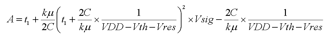
본 발명은, 표시하는 모든 계조에 있어서, 임계값 전압에 의한 전류값의 편차뿐만 아니라, 이동도에 의한 전류값의 편차가 휘도에 반영되는 것을 충분히 방지할 수 있다.The present invention can sufficiently prevent the deviation of the current value due to the threshold voltage, as well as the deviation of the current value due to the mobility, from being reflected in the luminance in all gradations to be displayed.
(실시형태 2)(Embodiment 2)
본 실시형태에서는, 본 발명의 표시 장치가 가지는 화소의 보다 구체적인 구성과, 그 동작에 대해서 설명한다.In the present embodiment, a more specific configuration of the pixel of the display device of the present invention and its operation will be described.
도 5a에, 본 실시형태에 있어서의 화소의 회로도를 나타낸다. 도 5a에 나타내는 화소(200)는, 발광 소자(201), 구동용 트랜지스터(202) 이외에도, 전위 Vsig를 가지는 비디오 신호의 샘플링을 행하는 스위칭용 트랜지스터(203)와, 구동용 트랜지스터(202)의 게이트(G)와 드레인(D)의 사이의 접속을 제어하는 트랜지스터(204)와, 구동용 트랜지스터(202)의 게이트(G)에 보정용 초기 전위 Vres가 주어지는 것을 제어하는 트랜지스터(205)와, 구동용 트랜지스터(202)의 드레인을 플로 팅 상태로 할지 아닐지를 선택하는 트랜지스터(206)와, 보정 기간에 있어서 구동용 트랜지스터(202)의 게이트와 소스간의 전압을 유지하기 위한 용량(207)과 표시 기간에 있어서 비디오 신호의 전위와 기준 전위의 전위 차이를 유지하기 위한 용량(208)을 가진다.5A shows a circuit diagram of a pixel in the present embodiment. The
또한, 본 실시형태에서는, 비디오 신호의 전위 Vsig 또는 전원 전위 VDD를 화소(200)에 공급하기 위한 신호 선 Si(i=1 내지 x)와, 보정용 초기 전위 Vres를 화소(200)에 공급하기 위한 리셋 선 Ri(i=1 내지 x)와, 전원 전위 VDD를 화소(200)에 공급하기 위한 전원선 Vi(i=1 내지 x)가, 화소(200)에 형성된다.In this embodiment, the signal line Si (i = 1 to x) for supplying the potential Vsig or the power source potential VDD of the video signal to the
스위칭용 트랜지스터(203)의 소스와 드레인은, 한쪽이 신호 선 Si에 접속되고, 다른 쪽은 용량(207)의 한쪽의 전극 및 용량(208)의 한쪽의 전극에 접속된다. 용량(208)의 다른 쪽의 전극은, 전원선 Vi에 접속된다. 또한, 용량(207)의 다른 쪽의 전극은, 구동용 트랜지스터(202)의 게이트에 접속된다. 구동용 트랜지스터(202)의 소스는, 전원선 Vi에 접속된다. 또한, 구동용 트랜지스터(202)의 드레인과 발광소자(201)의 사이에는, 트랜지스터(206)가 직렬로 접속된다. 트랜지스터(205)의 소스와 드레인은, 한쪽이 리셋 선 Ri에 접속되며, 다른 쪽이 구동용 트랜지스터(202)의 게이트에 접속된다. 또한, 트랜지스터(204)의 소스와 드레인은, 한쪽이 구동용 트랜지스터(202)의 게이트에 접속되고, 다른 쪽이 구동용 트랜지스터(202)의 드레인에 접속된다.One of the source and the drain of the switching
또한, 본 실시형태에서는, 스위칭용 트랜지스터(203)의 게이트에 접속된 주사 선 Gaj(j=1 내지 y)와, 트랜지스터(205)의 게이트에 접속된 주사 선 Gbj(j=1 내 지 y)와, 트랜지스터(204)의 게이트에 접속된 주사 선 Gcj(j=1 내지 y)와, 트랜지스터(206)의 게이트에 접속된 주사 선 Gbj(j=1 내지 y)가, 화소(200)에 형성된다.In this embodiment, the scanning line Gaj (j = 1 to y) connected to the gate of the switching
또한, 도 5a에서는, 구동용 트랜지스터(202)가 p형인 경우를 예시하지만, 본 발명은 이 구성에 한정되지 않는다. 구동용 트랜지스터(202)가 n형이라도 좋다. 다만, 본 실시형태에서는 구동용 트랜지스터(202)가 p형인 경우를 예를 들어 설명하기 때문에, 전원 전위 VDD(VDD>Vres)를 사용한다. 구동용 트랜지스터(202)가 n형의 경우에는, 전원 전위 VSS(Vres>VSS)를 사용한다.5A shows a case where the driving
또한, 도 5a에서는, 스위칭용 트랜지스터(203), 트랜지스터(204), 트랜지스터(205)가 n형, 트랜지스터(206)가 p형인 경우를 예시하지만, 본 발명은 이 구성에 한정되지 않는다. 스위칭용 트랜지스터(203), 트랜지스터(204 내지 206)는, n형이라도 p형이라도 좋다.5A shows a case where the switching
도 5b에 주사 선 Gaj, 주사 선 Gbj, 주사 선 Gcj, 주사 선 Gdj, 신호 선 S1, 신호 선 S2, 신호 선 S3, 리셋 선 R1, 리셋 선 R2, 리셋 선 R3에 주어지는 전위의 타이밍 차트를 나타낸다.5B shows a timing chart of potentials given to the scanning line Gaj, the scanning line Gbj, the scanning line Gcj, the scanning line Gdj, the signal line S1, the signal line S2, the signal line S3, the reset line R1, the reset line R2 and the reset line R3 .
우선 초기화 기간에서는, 주사 선 Gaj, 주사 선 Gbj, 주사 선 Gcj, 주사 선 Gdj에 하이 레벨의 전위가 주어지기 때문에, 스위칭용 트랜지스터(203)는 온, 트랜지스터(204)는 온, 트랜지스터(205)는 온, 트랜지스터(206)는 오프가 된다. 그리고, 신호 선 S1, 신호 선 S2, 신호 선 S3에는 전원 전위 VDD가 주어진다. 또한, 리셋 선 R1, 리셋 선 R2, 리셋 선 R3에는, 각각 보정용 초기 전위 Vres1, Vres2, Vres3가 주어진다. 다만, 본 실시형태에서는, |VDD-Vres1|<|VDD-Vres2|<| VDD-Vres3|인 경우를 예시한다. 용량(207)에는, 보정용 초기 전위와 전원 전위 VDD의 전위 차이가 유지된다.The switching
다음, 보정 기간에서는, 주사 선 Gaj, 주사 선 Gcj, 주사 선 Gdj에 하이 레벨의 전위가 주어지고, 주사 선 Gbj에는 로 레벨의 전위가 주어지기 때문에, 스위칭용 트랜지스터(203)는 온, 트랜지스터(204)는 온, 트랜지스터(205)는 오프, 트랜지스터(206)는 오프이다. 그리고 신호 선 S1, 신호 선 S2, 신호 선 S3에서는, 전원 전위 VDD가 주어지는 채로이다. 또한, 리셋 선 R1, 리셋 선 R2, 리셋 선 R3에는, 각각 보정용 초기 전위 Vres1, Vres2, Vres3가 주어진 채로이다. 보정 기간에서는, 용량(207)에 축적한 전하가 시간이 지나감에 따라 방출된다. 따라서, 최종적으로는, 용량(207)에 보정용 초기 전위 Vres1, Vres2, Vres3에 맞추는 값의 게이트 전압 Vgs가 유지된다. 구체적으로는, 보정용 초기 전위 Vres1가 화소에 주어질 때에, 보정 기간의 종료 직전에 용량(207)에 유지되는 게이트 전압 Vgs를 |Vr1+Vth|로 한다. 또한, 보정용 초기 전위 Vres2가 화소에 주어질 때에 보정 기간의 종료 직전에 용량(207)에 유지되는 게이트 전압 Vgs를 |Vr2+Vth|로 한다. 또한, 보정용 초기 전위 Vres3가 화소에 주어질 때에, 보정 기간의 종료 직전에 용량(207)에 유지되는 게이트 전압 Vgs를 |Vr3+Vth|로 한다. 다만, |VDD-Vres1|<|VDD-Vres2|<|VDD-Vres3|이기 때문에, |Vr1+Vth|<|Vr2+Vth|<|Vr3+Vth|가 된다.Next, in the correction period, a high level potential is given to the scanning line Gaj, the scanning line Gcj, and the scanning line Gdj, and a low level potential is given to the scanning line Gbj, so that the switching
다음, 표시 기간이 가지는 기록 기간에서는, 주사 선 Gaj, 주사 선 Gdj에 하이 레벨의 전위가 주어지고, 주사 선 Gbj, 주사 선 Gcj에는 로 레벨의 전위가 주어 지기 때문에, 스위칭용 트랜지스터(203)는 온, 트랜지스터(204)는 오프, 트랜지스터(205)는 오프, 트랜지스터(206)는 오프이다. 그리고 신호 선 S1, 신호 선 S2, 신호 선 S3에는, 비디오 신호의 전위 Vsig가 주어진다. 본 발명에서는, 표시 기간에 화소(200)에 주어지는 비디오 신호의 전위 Vsig와 기준 전위(본 실시형태에서는 전원 전위 VDD)와의 차이가 보다 작을수록, 보정용 초기 전위 Vres와 기준 전위(본 실시형태에서는 전원 전위 VDD)와의 차이를 보다 작게 한다. 따라서, 도 5b에 나타내는 타이밍 차트에서는, 신호 선 S1, 신호 선 S2, 신호 선 S3에 주어지는 비디오 신호의 전위를 각각 Vsig1, Vsig2, Vsig3로 하면, |VDD-Vsig1|<|VDD-Vsig2|<|VDD-Vsig3|가 된다. 본 실시형태에서는, 보정용 초기 전위 Vsig1, Vsig2, Vsig3는 부의 값을 가지기 때문에, Vsig1>Vsig2>Vsig3이 된다. 비디오 신호의 전위 Vsig1, Vsig2, Vsig3와 기준 전위(본 실시형태에서는 전원 전위 VDD)의 전위 차이는, 각 화소(200)의 용량(208)에 유지된다.Next, in the writing period of the display period, since the scanning line Gaj and the scanning line Gdj are given a high-level potential and the scanning line Gbj and the scanning line Gcj are given a low-level potential, the switching
다음, 표시 기간이 가지는 발광 기간에는, 주사 선 Gaj, 주사 선 Gbj, 주사 선 Gcj, 주사 선 Gdj에 로 레벨의 전위가 주어지기 때문에, 스위칭용 트랜지스터(203)는, 오프, 트랜지스터(204)는 오프, 트랜지스터(205)는 오프, 트랜지스터(206)는 온이다. 구동용 트랜지스터(202)에는, 용량(208)에 유지되는 비디오 신호의 전위와 기준 전위(본 실시형태에서는 전원 전위 VDD)의 전위 차이에 용량(207)에 유지되는 전압을 뺀 전압이 게이트 전압으로서 주어진다. 그리고, 각 화소(200)의 발광 소자(201)에는, 구동용 트랜지스터(202)의 게이트 전압에 맞은 값의 전류가 공급되고, 발광 소자(201)는 계조의 표시를 행한다.Next, in the light emission period of the display period, since the low level electric potential is given to the scanning line Gaj, the scanning line Gbj, the scanning line Gcj and the scanning line Gdj, the switching
본 발명에서는, 보정용 초기 전위 Vres의 값을, 표시 기간에 주어지는 비디오 신호의 전위 Vsig의 값에 따라 변경시킨다. 따라서, 높은 계조를 표시하는 경우는, 이동도의 편차에 기인하는 전류값의 변동의 보정을 효과적으로 행할 수 있다. 또한, 낮은 계조를 표시하는 경우에는, 전위 Vsig와 기준 전위의 차이가 작아질수록 구동용 트랜지스터의 드레인 전류가 0에 보다 가까워질 수 있다. 따라서, 높은 계조를 표시하는 경우뿐만 아니라, 낮은 계조를 표시하는 경우라도, 이동도의 편차에 의하여 생기는 구동용 트랜지스터의 전류값의 변동을 억제할 수 있고, 나아가서는 상기 변동에 기인하는 휘도의 편차를 억제할 수 있다.In the present invention, the value of the initial potential for correction Vres is changed in accordance with the value of the potential Vsig of the video signal given in the display period. Therefore, in the case of displaying a high gradation, it is possible to effectively correct the fluctuation of the current value due to the deviation of the mobility. Further, in the case of displaying a low gradation, the drain current of the driving transistor can be made closer to 0 as the difference between the potential Vsig and the reference potential becomes smaller. Therefore, not only in the case of displaying a high gray level but also in a case of displaying a low gray level, it is possible to suppress the fluctuation of the current value of the driving transistor caused by the deviation of the mobility, Can be suppressed.
따라서, 본 발명은, 표시하는 모든 계조에 있어서, 임계값 전압에 의한 전류값의 편차뿐만 아니라, 이동도에 의한 전류값의 편차가 휘도에 반영되는 것을 충분히 방지할 수 있다.Therefore, the present invention can sufficiently prevent the deviation of the current value due to the threshold voltage, as well as the deviation of the current value due to the mobility, from being reflected in the luminance in all gradations to be displayed.
또한, 보다 정확하게 이동도 μ의 편차에 기인하는, 구동용 트랜지스터의 전류값의 편차를 보정하기 위해서는, 실시형태 1에서 나타내는 수식 5에 있어서, 좌변의 A가 가장 0에 가까워지도록, 비디오 신호의 전위 Vsig의 값에 맞추어 보정용 초기 전위 Vres의 값을 설정하면 좋다.Further, in order to correct the deviation of the current value of the driving transistor due to the deviation of the mobility μ more accurately, it is preferable that in the equation 5 shown in the first embodiment, the potential of the video signal The value of the initial potential for correction Vres may be set in accordance with the value of Vsig.
본 실시형태는, 상기 실시형태와 적절히 조합하여 실시할 수 있다.The present embodiment can be implemented in appropriate combination with the above embodiment.
(실시형태 3)(Embodiment 3)
본 실시형태에서는, 본 발명의 표시 장치가 가지는 화소의 보다 구체적인 구성과, 그 동작에 대해서 설명한다.In the present embodiment, a more specific configuration of the pixel of the display device of the present invention and its operation will be described.
도 6a에, 본 실시형태에 있어서의 화소의 회로도를 나타낸다. 도 6a에 나타 내는 화소(300)는, 발광 소자(301), 구동용 트랜지스터(302) 이외에 전위 Vsig를 가지는 비디오 신호의 샘플링을 행하는 스위칭용 트랜지스터(303)와, 구동용 트랜지스터(302)의 게이트(G)와 드레인(D)간의 접속을 제어하는 트랜지스터(304)와, 구동용 트랜지스터(302)의 게이트(G)에 보정용 초기 전위(Vres)가 주어지는 것을 제어하는 트랜지스터(305)와 구동용 트랜지스터(302)의 드레인을 플로팅 상태로 할지 아닐지를 선택하는 트랜지스터(306)와, 보정 기간에 있어서 구동용 트랜지스터(302)의 게이트와 소스간의 전압을 유지하기 위한 용량(307)과, 표시 기간에 있어서 비디오 신호의 전위와 기준 전위의 전위 차이를 유지하기 위한 용량(308)과, 구동용 트랜지스터(302)의 소스를 플로팅 상태로 할지 아닐지를 선택하는 트랜지스터(309)와, 용량(308)의 한쪽의 전극에의 전원 전위 VDD의 공급을 제어하는 트랜지스터(310)를 가진다.6A shows a circuit diagram of a pixel in the present embodiment. The
또한, 본 실시형태에서는, 비디오 신호의 전위 Vsig 또는 전원 전위 VDD를 화소(300)에 공급하기 위한 신호 선 Si(i=1 내지 x)와, 보정용 초기 전위 Vres를 화소(300)에 공급하기 위한 리셋 선 Ri(i=1 내지 x)와, 전원 전위 VDD를 화소(300)에 공급하기 위한 전원선 Vai(i=1 내지 x)와, 전원 전위 VDD'를 화소(300)에 공급하기 위한 전원선 Vbi(i=1 내지 x)가 화소(300)에 형성된다. 다만, VDD'≤VDD로 한다.(I = 1 to x) for supplying the potential Vsig of the video signal or the power source potential VDD to the
스위칭용 트랜지스터(303)의 소스와 드레인은, 한쪽이 신호 선 Si에 접속되고, 다른 쪽은 용량(308)의 한쪽의 전극에 접속된다. 용량(308)의 다른 쪽의 전극은, 구동용 트랜지스터(302)의 게이트 및 용량(307)의 한쪽의 전극에 접속된다. 용량(307)의 다른 쪽의 전극은, 구동용 트랜지스터(302)의 소스에 접속된다. 트랜지스터(304)의 소스와 드레인은, 한쪽이 구동용 트랜지스터(302)의 게이트에 접속되고, 다른 쪽이 구동용 트랜지스터(302)의 드레인에 접속된다. 트랜지스터(306)의 소스와 드레인은, 한쪽이 전원선 Vai에, 다른 쪽은 구동용 트랜지스터(302)의 드레인에 접속된다. 트랜지스터(305)의 소스와 드레인은, 한쪽이 리셋 선 Ri에, 다른 쪽이 구동용 트랜지스터(302)의 소스에 접속된다. 트랜지스터(309)의 소스와 드레인은, 한쪽이 구동용 트랜지스터(302)의 소스에, 다른 쪽이 발광 소자(301)에 접속된다. 트랜지스터(310)의 소스와 드레인은, 한쪽이 용량(308)의 한쪽의 전극에, 다른 쪽이 전원선 Vbi에 접속된다.One of the source and the drain of the switching
또한, 본 실시형태에서는, 스위칭용 트랜지스터(303)의 게이트에 접속된 주사 선 Gaj(j=1 내지 y)와, 트랜지스터(305)의 게이트에 접속된 주사 선 Gbj(j=1 내지 y)와, 트랜지스터(304)의 게이트에 접속된 주사 선 Gcj(j=1 내지 y)와, 트랜지스터(306)의 게이트에 접속된 주사 선 Gdj(j=1 내지 y)와, 트랜지스터(309)의 게이트에 접속된 주사 선 Gej(j=1 내지 y)가, 화소(300)에 형성된다.In this embodiment, the scanning lines Gaj (j = 1 to y) connected to the gates of the switching
또한, 도 6a에서는, 구동용 트랜지스터(302)가 n형인 경우를 예시하지만, 본 발명은 이 구성에 한정되지 않는다. 구동용 트랜지스터(302)가 p형이라도 좋다. 다만, 본 실시형태에서는, 구동용 트랜지스터(302)가 n형의 경우를 예를 들어 설명하기 때문에, 전원선 Vai에 전원 전위 VDD가, 전원선 Vbi에 전원 전위 VDD'가 주어진다. 또한, VDD≥VDD'>Vres로 한다. 구동용 트랜지스터(302)가 p형인 경우는, 전원선 Vai에 전원 전위 VSS가, 전원선 Vbi에 전원 전위 VSS'를 준다. 또한, Vres>VSS'≥VSS로 한다.In Fig. 6A, the case where the driving
또한, 도 6a에서는, 스위칭용 트랜지스터(303), 트랜지스터(304), 트랜지스터(305), 트랜지스터(310)가 n형, 트랜지스터(306), 트랜지스터(309)가 p형인 경우를 예시하지만, 본 발명은 이 구성에 한정되지 않는다. 스위칭용 트랜지스터(303), 트랜지스터(304 내지 306), 트랜지스터(309), 트랜지스터(310)는 n형이라도 p형이라도 좋다.6A shows a case where the switching
도 6b에, 주사 선 Gaj, 주사 선 Gbj, 주사 선 Gcj, 주사 선 Gdj, 주사 선 Gej, 신호 선 S1, 신호 선 S2, 신호 선 S3, 리셋 선 R1, 리셋 선 R2, 리셋 선 R3에 주어지는 전위의 타이밍 차트를 나타낸다.6B, potentials given to the scanning line Gaj, the scanning line Gbj, the scanning line Gcj, the scanning line Gdj, the scanning line Gej, the signal line S1, the signal line S2, the signal line S3, the reset line R1, the reset line R2, Fig.
우선, 초기화 기간에서는, 주사 선 Gaj, 주사 선 Gdj에 로 레벨의 전위, 주사 선 Gbj, 주사 선 Gcj, 주사 선 Gej에 하이 레벨의 전위가 주어지기 때문에, 스위칭용 트랜지스터(303)는 오프, 트랜지스터(304)는 온, 트랜지스터(305)는 온, 트랜지스터(306)는 온, 트랜지스터(309)는 오프, 트랜지스터(310)는 온이 된다. 그리고, 리셋 선 R1, 리셋 선 R2, 리셋 선 R3에는, 각각 보정용 초기 전위 Vres1, Vres2, Vres3가 주어진다. 다만, 본 실시형태에서는, |VDD-Vres1|<|VDD-Vres2|<|VDD-Vres3|인 경우를 예시한다. 용량(307)에는, 보정용 초기 전위와 전원 전위 VDD의 전위 차이가 유지된다.First, in the initializing period, since the high level potential is given to the scanning line Gaj, the low level potential to the scanning line Gdj, the scanning line Gbj, the scanning line Gcj, and the scanning line Gej, the switching
다음, 보정 기간에서는, 주사 선 Gaj, 주사 선 Gbj, 주사 선 Gdj에 로 레벨의 전위가 주어지고, 주사 선 Gcj, 주사 선 Gej에는 하이 레벨의 전위가 주어지기 때문에, 스위칭용 트랜지스터(303)는 오프, 트랜지스터(304)는 온, 트랜지스 터(305)는 오프, 트랜지스터(306)는 온, 트랜지스터(309)는 오프, 트랜지스터(310)는 온이다. 리셋 선 R1, 리셋 선 R2, 리셋 선 R3에는, 각각 보정용 초기 전위 Vres1, Vres2, Vres3가 주어지는 채로이다. 보정 기간에서는, 용량(307)에 축적한 전하가 시간에 따라 방출된다. 따라서, 최종적으로는, 용량(307)에 보정용 초기 전위 Vres1, Vres2, Vres3에 맞은 값의 게이트 전압 Vgs가 유지된다. 구체적으로는, 보정용 초기 전위 Vres1가 화소에 주어질 때에, 보정 기간이 종료되는 직전에 용량(307)에 유지되는 게이트 전압 Vgs를 |Vr1+Vth|로 한다. 또한, 보정용 초기 전위 Vres2가 화소에 주어질 때에, 보정 기간의 종료 직전에 용량(307)에 유지되는 게이트 전압 Vgs를 |Vr2+Vth|로 한다. 또한, 보정용 초기 전위 Vres3가 화소에 주어질 때에, 보정 기간의 종료 직전에 용량(307)에 유지되는 게이트 전압 Vgs를 |Vr3+Vth|로 한다. 다만, |VDD-Vres1|<|VDD-Vres2|<|VDD-sVres3|이기 때문에, |Vr1+Vth|<|Vr2+Vth|<|Vr3+Vth|가 된다. 또한, 용량(308)에는, 전원 전위 VDD와 전원 전위 VDD'의 전위 차이가 유지된다.Next, in the correction period, the low level potential is given to the scanning line Gaj, the scanning line Gbj, and the scanning line Gdj, and the high level potential is given to the scanning line Gcj and the scanning line Gej, The
다음, 표시 기간이 가지는 기록 기간에서는, 주사 선 Gcj, 주사 선 Gdj에 로 레벨의 전위가 주어지고, 주사 선 Gaj, 주사 선 Gbj, 주사 선 Gej에는 하이 레벨의 전위가 주어지기 때문에, 스위칭용 트랜지스터(303)는 온, 트랜지스터(304)는 오프, 트랜지스터(305)는 온, 트랜지스터(306)는 온, 트랜지스터(309)는 오프, 트랜지스터(310)는 오프이다. 그리고 신호 선 S1, 신호 선 S2, 신호 선 S3에는, 비디오 신호의 전위 Vsig가 주어진다. 본 발명에서는, 표시 기간에 화소(300)에 주어지는 비디오 신호의 전위 Vsig와 기준 전위(본 실시형태에서는 발광 소자(301)가 가지는 공통 전극의 전위 VSS)의 차이가 작을수록, 보정용 초기 전위 Vres와 기준 전위(본 실시형태에서는 전원 전위 VDD)의 차이가 보다 작아진다. 따라서, 도 6b에 나타내는 타이밍 차트에서는, 신호 선 S1, 신호 선 S2, 신호 선 S3에 주어지는 비디오 신호의 전위를 각각 Vsig1, Vsig2, Vsig3로 하면, |Vsig1-VSS|<|Vsig2-VSS||Vsig3-VSS|가 된다. 전원 전위 VDD와 전원 전위 VDD'의 전위 차이에 비디오 신호의 전위 Vsig1, Vsig2, Vsig3가 가산된 전위와, 기준 전위(본 실시형태에서는 전원 전위 VDD)의 전위 차이가 각 화소(300)의 용량(308)에 유지된다.Next, in the writing period of the display period, a low level potential is given to the scanning line Gcj and the scanning line Gdj, and a high level potential is given to the scanning line Gaj, the scanning line Gbj, and the scanning line Gej, The
다음, 표시 기간이 가지는 발광 기간에서는, 주사 선 Gaj, 주사 선 Gbj, 주사 선 Gcj, 주사 선 Gdj, 주사 선 Gej에 로 레벨의 전위가 주어지기 때문에, 스위칭용 트랜지스터(303)는 오프, 트랜지스터(304)는 오프, 트랜지스터(305)는 오프, 트랜지스터(306)는 온, 트랜지스터(309)는 온, 트랜지스터(310)는 오프이다. 구동용 트랜지스터(302)에는, 용량(308)에 유지되는 전압에, 용량(307)에 유지되는 전압을 뺀 전압이 게이트 전압으로서 주어진다. 그리고 각 화소(300)의 발과 소자(301)에는, 구동용 트랜지스터(302)의 게이트 전압에 맞은 값의 전류가 공급되고, 발광 소자(301)는 계조의 표시를 행한다.Next, in the light emission period of the display period, since the low level potential is given to the scanning line Gaj, the scanning line Gbj, the scanning line Gcj, the scanning line Gdj, and the scanning line Gej, the switching
본 발명에서는, 보정용 초기 전위 Vres의 값을 표시 기간에 주어지는 비디오 신호의 전위 Vsig의 값에 따라 변화시킨다. 따라서, 높은 계조를 표시하는 경우는, 이동도의 편차에 기인하는 전류값의 변동의 보정을 효율적으로 행할 수 있다. 또한, 낮은 계조를 표시하는 경우는, 전위 Vsig와 기준 전위의 차이가 작아질수록 구동용 트랜지스터의 드레인 전류가 0에 보다 가까워질 수 있다. 따라서, 높은 계 조를 표시하는 경우뿐만 아니라, 낮은 계조를 표시하는 경우이라도, 이동도의 편차에 의하여 생기는 구동용 트랜지스터의 전류값의 변동을 억제할 수 있고, 나아가서는, 상기 변동에 기인하는 휘도의 편차를 억제할 수 있다.In the present invention, the value of the initial potential for correction Vres is changed in accordance with the value of the potential Vsig of the video signal given in the display period. Therefore, when a high gradation is displayed, the variation of the current value due to the deviation of the mobility can be efficiently corrected. Further, in the case of displaying a low gradation, the drain current of the driving transistor can become closer to 0 as the difference between the potential Vsig and the reference potential becomes smaller. Therefore, not only in the case of displaying a high gradation but also in the case of displaying a low gradation, the fluctuation of the current value of the driving transistor caused by the deviation of the mobility can be suppressed, and furthermore, Can be suppressed.
또한, 전원 전위 VDD=전원 전위 VDD'이의 경우, 전원선 Vbi를 형성하지 않고, 트랜지스터(306)의 소스와 드레인의 어느 한쪽을 전원선 Vai에, 다른 쪽을 구동용 트랜지스터(302)의 드레인에 접속하도록 하여도 좋다. 이 경우, 화소부에 형성되는 배선의 수를 삭감하고, 수율을 향상시키고, 또한, 화소의 개구율을 향상시킬 수 있다. 또한, 전원 전위 VDD>전원 전위 VDD'의 경우, 전원선 Vbi는 필요하게 된다. 이 경우, 보정 기간에 있어서, 용량(308)에 유지된 전압에 의하여, 스위칭용 트랜지스터(303)가 온이 될 때에, 신호 선의 전위가 불필요하게 높아지는 것을 방지할 수 있다.When the power source potential VDD is equal to the power source potential VDD ', the power source line Vbi is not formed and either the source or the drain of the
또한, 보다 정확하게 이동도 μ의 편차에 기인하는 구동용 트랜지스터의 전류값의 편차를 보정하는 경우에는, 실시형태 1에서 나타낸 수식 5에 있어서, 좌변의 A가 가장 0에 가까워지도록 비디오 신호의 전위 Vsig의 값에 맞추어 보정용 초기 전위 Vres의 값을 설정하면 좋다.Further, in the case of correcting the deviation of the current value of the driving transistor due to the deviation of the mobility μ more accurately, in the equation 5 shown in the first embodiment, the potential Vsig of the video signal The value of the initial potential for correction Vres may be set in accordance with the value of [
따라서, 본 발명은 표시하는 모든 계조에 있어서, 임계값 전압에 의한 전류값의 편차뿐만 아니라, 이동도에 의한 전류값의 편차가 휘도에 반영되는 것을 충분히 방지할 수 있다.Therefore, according to the present invention, not only the deviation of the current value due to the threshold voltage but also the deviation of the current value due to the mobility can be sufficiently prevented from being reflected in the luminance in all gradations to be displayed.
본 실시형태는, 상기 실시형태와 적절히 조합하여 실시할 수 있다.The present embodiment can be implemented in appropriate combination with the above embodiment.
(실시형태 4)(Fourth Embodiment)
본 실시형태에서는, 본 발명의 표시 장치의 전체적인 구성에 대해서 설명한다. 도 7에, 본 실시형태의 표시 장치의 블록도를 일례로서 나타낸다.In the present embodiment, the overall configuration of the display device of the present invention will be described. Fig. 7 shows a block diagram of the display device of the present embodiment as an example.
도 7에 나타내는 표시 장치는, 발광 소자를 구비한 화소를 복수 가지는 화소부(500)와, 각 화소를 라인마다 선택하는 주사 선 구동 회로(510)와 선택된 라인의 화소에의 비디오 신호의 입력을 제어하는 신호 선 구동 회로(520)와, 선택된 라인의 화소에의 보정용 초기 전위의 입력을 제어하는 리셋 선 구동 회로(530)를 가진다.7 includes a
도 7에 있어서, 신호 선 구동 회로(520)는, 시프트 레지스터(521), 제 1 래치(522), 제 2 래치(523), DA(Digital to Analog)변환회로(524)를 가진다. 시프트 레지스터(521)에는, 클록 신호 S-CLK, 스타트 펄스 신호 S-SP가 입력된다. 시프트 레지스터(521)는, 이들의 클록 신호 S-CLK 및 스타트 펄스 신호 S-SP에 따라, 펄스가 순차로 시프트하는 타이밍 신호를 생성하여, 제 1 래치(522)에 출력한다. 타이밍 신호의 펄스가 출현하는 순서는, 주사 방향 전환 신호에 따라 바꾸도록 하여도 좋다.7, the signal
제 1 래치(522)에 타이밍 신호가 입력되면, 상기 타이밍 신호의 펄스에 따라, 비디오 신호가 순차로 제 1 래치(522)에 기록되어 유지된다. 또한, 제 1 래치(522)가 가지는 복수의 기억 회로에 순차로 비디오 신호를 기록하여도 좋지만, 제 1 래치(522)가 가지는 복수의 기억 회로를 여러 그룹으로 분할하고, 상기 그룹마다 병행하여 비디오 신호를 입력하는, 이른바 분할 구동을 행하여도 좋다. 또한, 이 때의 그룹수를 분할수라고 부른다. 예를 들면, 래치 중의 기억 회로를 4개 의 그룹으로 분할한 경우, 4분할로 분할 구동할 수 있다.When a timing signal is input to the
제 1 래치(522)의 모든 기억 회로에의 비디오 신호의 기록이 한차례 종료될 때까지의 시간을 라인 기간이라고 부른다. 실제로는, 상기 라인 기간에 수평 귀선 기간(水平歸線期間)이 더해지는 기간을 라인 기간에 포함하는 경우가 있다.The time until the recording of the video signal to all the memory circuits of the
1라인 기간이 종료되면, 제 2 래치(523)에 입력되는 래치 신호 S-LS의 펄스에 따라, 제 1 래치(522)에 유지되는 비디오 신호가, 제 2 래치(523)에 일제히 기록되어, 유지된다. 비디오 신호를 제 2 래치(523)에 모두 송출한 제 1 래치(522)에는, 다시 시프트 레지스터(521)로부터의 타이밍 신호에 따라, 다음 비디오 신호의 기록이 순차로 행해진다. 이 2순째의 1라인 기간 중에는, 제 2 래치(523)에 기록되어 유지되는 비디오 신호가, DA변환 회로(524)에 입력된다.The video signal held in the
그리고 DA 변환 회로(524)는, 입력된 디지털의 비디오 신호를 아날로그의 비디오 신호로 변환하고, 신호 선을 통하여 화소부(500) 내의 각 화소에 입력한다.The
또한, 신호 선 구동회로(520)는, 시프트 레지스터(521) 대신에, 펄스가 순차로 시프트하는 신호를 출력할 수 있는 다른 회로를 사용하여도 좋다.Instead of the
또한, 도 7에서는 DA변환 회로(524)의 후단에 화소부(500)가 직접 접속되지만, 본 발명은 이 구성에 한정되지 않는다. 화소부(500)의 전단에, DA 변환 회로(524)로부터 출력된 비디오 신호에 신호 처리를 행하는 회로를 형성할 수 있다. 신호 처리를 행하는 회로의 일례로서, 예를 들면, 파형을 정형할 수 있는 버퍼 등을 들 수 있다.7, the
또한, 리셋 선 구동 회로(530)는 신호 선 구동 회로(520)와 마찬가지로, 시 프트 레지스터(531), 제 1 래치(532), 제 2 래치(533), DA변환 회로(534)를 가진다. 시프트 레지스터(531)에는, 클록 신호 R-CLK, 스타트 펄스 신호 R-SP가 입력된다. 시프트 레지스터(531)는, 이들의 클록 신호 R-CLK 및 스타트 펄스 신호 R-SP에 따라, 펄스가 순차로 시프트하는 타이밍 신호를 생성하고, 제 1 래치(532)에 출력한다. 타이밍 신호의 펄스가 출현하는 순서는, 주사 방향 전환 신호에 따라 바꿔도 좋다. 다만, 리셋 선 구동 회로(530)에 있어서의 타이밍 신호의 펄스가 출현하는 순서는, 신호 선 구동 회로(520)에 있어서의 타이밍 신호의 펄스가 출현하는 순서에 맞추어 결정한다.Like the signal
제 1 래치(532)에 타이밍 신호가 입력되면, 상기 타이밍 신호의 펄스에 따라, 리셋 신호가 순차로 제 1 래치(532)에 기록되어, 유지된다. 또한, 제 1 래치(532)가 가지는 복수의 기억 회로에 순차로 리셋 신호를 기록하여도 좋지만, 제 1 래치(532)가 가지는 복수의 기억 회로를 여러 그룹으로 분할하고, 상기 그룹마다 병행하여 리셋 신호를 입력하는, 이른바 분할 구동을 행하여도 좋다. 또한, 이 때의 그룹수를 분할수라고 부른다. 예를 들면, 래치 중의기억 회로를 4개의 그룹으로 분할하는 경우, 4분할로 분할 구동할 수 있다.When a timing signal is input to the
제 1 래치(532)의 모든 기억 회로에의 리셋 신호의 기록이 한차례 종료될 때까지의 시간을 라인 기간이라고 부른다. 실제로는, 상기 라인 기간에 수평 귀선 기간이 더해지는 기간을 라인 기간에 포함하는 경우도 있다.The time until the writing of the reset signal to all the memory circuits of the
1라인 기간이 종료되면, 제 2 래치(533)에 입력되는 래치 신호 R-LS의 펄스에 따라, 제 1 래치(532)에 유지되는 리셋 신호가 제 2 래치(533)에 일제히 기록되 어, 유지된다. 리셋 신호를 제 2 래치(533)에 모두 송출한 제 1 래치(532)에는, 다시 시프트 레지스터(531)로부터의 타이밍 신호에 따라, 다음 리셋 신호의 기록이 순차로 행해진다. 이 2순째의 1라인 기간 중에는, 제 2 래치(533)에 기록되어 유지되는 리셋 신호가, DA 변환 회로(534)에 입력된다.The reset signal held in the
그리고 DA 변환 회로(534)는, 입력된 디지털의 리셋 신호를 아날로그의 리셋 신호로 변환한다. 아날로그의 리셋 신호의 전위가, 보정용 초기 전위로서 리셋 선을 통하여 화소부(500) 내의 각 화소에 DA 변환 회로(534)로부터 입력된다.The
또한, 리셋 선 구동 회로(530)는, 시프트 레지스터(531) 대신에, 펄스가 순차로 시프트하는 신호를 출력할 수 있는 다른 회로를 사용하여도 좋다.The reset
또한, 도 7에서는, DA 변환 회로(534)의 후단에 화소부(500)가 직접 접속되지만, 본 발명은 이 구성에 한정되지 않는다. 화소부(500)의 전단에, DA 변환 회로(534)로부터 출력된 리셋 신호에 신호 처리를 행하는 회로를 형성할 수 있다. 신호 처리를 행하는 회로의 일례로서, 예를 들면, 파형을 정경할 수 있는 버퍼 등을 들 수 있다.7, the
다음, 주사 선 구동 회로(510)의 동작에 대해서 설명한다. 본 발명의 표시 장치에서는, 화소부(500)의 각 화소에 주사 선이 복수 형성된다. 주사 선 구동 회로(510)는 선택 신호를 생성하고, 상기 선택 신호를 복수의 각 주사 선에 입력함으로써, 화소를 라인마다 선택한다. 선택 신호에 의하여 화소가 선택되면, 주사 선의 하나에 게이트가 접속된 스위칭용 트랜지스터가 온이 되고, 화소에의 비디오 신호의 입력이 행해진다. 또한, 선택 신호에 의하여 화소가 선택되면, 주사 선의 하 나에 게이트가 접속된, 보정용 초기 전위의 공급을 제어하는 트랜지스터가 온이 되고, 화소에의 리셋 신호의 입력이 행해진다. 또한, 선택 신호에 의하여 상기 이외에 화소에 형성된 스위칭 소자로서 기능하는 트랜지스터의 스위칭 소자가 제어된다.Next, the operation of the scanning
또한, 본 실시형태에서는, 복수의 주사 선에 입력되는 선택 신호를 모든 하나의 주사 선 구동 회로(510)로 생성하는 예에 대해서 설명하지만, 본 발명은 이 구성에 한정되지 않는다. 복수의 주사 선 구동 회로(510)로 복수의 주사 선에 입력되는 선택 신호의 생성을 행하여도 좋다.In the present embodiment, an example of generating a selection signal to be inputted to a plurality of scanning lines by all one scanning
또한, 화소부(500), 주사 선 구동 회로(510), 신호 선 구동 회로(520), 리셋 선 구동 회로(530)는, 같은 기판에 형성할 수 있지만, 어느 것을 다른 기판에 형성할 수도 있다.The
본 실시형태는, 상기 실시형태와 적절히 조합하여 실시할 수 있다.The present embodiment can be implemented in appropriate combination with the above embodiment.
(실시형태 5)(Embodiment 5)
본 실시형태에서는, 본 발명의 표시 장치의 전체적인 구성에 대해서 설명한다. 도 8에, 본 실시형태의 표시 장치의 블록도를 일례로서 나타낸다.In the present embodiment, the overall configuration of the display device of the present invention will be described. 8 shows a block diagram of the display device of the present embodiment as an example.
도 8에 나타내는 본 발명의 표시 장치는, 복수의 화소를 가지는 화소부(600)와, 복수의 화소를 라인마다 선택할 수 있는 주사 선 구동 회로(610)와, 선택된 라인 내의 화소에의 비디오 신호의 입력을 제어하는 신호 선 구동 회로(620)와, 선택된 라인 내의 화소에의 리셋 신호의 입력을 제어하는 리셋 선 구동 회로(630)를 가진다.The display device of the present invention shown in Fig. 8 includes a
신호 선 구동 회로(620)는, 시프트 레지스터(621)와, 샘플링 회로(622)와, 아날로그 신호를 기억할 수 있는 래치(623)를 적어도 가진다. 시프트 레지스터(621)에 클록 신호 S-CLK와 스타트 펄스 신호 S-SP가 입력된다. 시프트 레니스터(621)는 이들의 클록 신호 S-LCK 및 스타트 펄스 신호 S-SP에 따라, 펄스가 순차로 시프트하는 타이밍 신호를 생성하여, 샘플링 회로(622)에 입력한다. 샘플링 회로(622)에서는, 입력된 타이밍 신호에 따라, 신호 선 구동 회로(620)에 입력된 1라인 기간분의 아날로그의 비디오 신호를 샘플링한다. 그리고 1라인 기간분의 비디오 신호가 모두 샘플링되면, 샘플링된 비디오 신호는 래치 신호 S-LS에 따라 일제히 래치(623)에 출력되어 유지된다. 래치(623)에 유지되는 비디오 신호는, 신호 선을 통하여 화소부(600)에 입력된다.The signal
또한, 본 실시형태에서는, 샘플링 회로(622)에 있어서 1라인 기간분의 비디오 신호를 모두 샘플링한 후에, 일제히 하단(下段)의 래치(623)에 샘플링된 비디오 신호를 입력하는 경우를 예를 들어 설명하지만, 본 발명은 이 구성에 한정되지 않는다. 샘플링 회로(622)에 있어서 각 화소에 대응하는 비디오 신호를 샘플링하면, 1라인 기간분의 비디오 신호가 모두 샘플링되는 것을 기다리지 않고, 그 때마다 하단의 래치(623)에 샘플링된 비디오 신호를 입력하여도 좋다.In the present embodiment, the case where all the video signals for one line period are sampled in the
또한, 비디오 신호의 샘플링은 대응하는 화소마다 행하여도 좋고, 1라인 내의 화소를 여러 그룹으로 분할하고 각 그룹에 대응하는 화소마다 병행하여 행하여도 좋다.The sampling of the video signal may be performed for each corresponding pixel, or the pixels within one line may be divided into a plurality of groups and performed in parallel for each pixel corresponding to each group.
또한, 도 8에서 래치(623)의 후단에 직접 화소부(600)가 접속되지만, 본 발 명은 이 구성에 한정되지 않는다. 화소부(600)의 전단에, 래치(623)로부터 출력된 아날로그의 비디오 신호에 신호 처리를 행하는 회로를 형성할 수 있다. 신호 처리를 행하는 회로의 일례로서, 예를 들면, 파형을 정경할 수 있는 버퍼 등을 들 수 있다.8, the
그리고, 래치(623)로부터 화소부(600)에 비디오 신호가 입력되는 것과 병행하여, 샘플링 회로(622)는 다음 라인 기간에 대응하는 비디오 신호를 다시 샘플링할 수 있다.In parallel with the input of the video signal from the
또한, 리셋 선 구동 회로(630)는 신호 선 구동 회로(620)와 같이, 시프트 레지스터(631)와, 샘플링 회로(632)와, 아날로그 신호를 기억할 수 있는 래치(633)를 적어도 가진다. 시프트 레지스터(631)에 클록 신호 R-CLK와, 스타트 펄스 신호 R-SP가 입력된다. 시프트 레지스터(631)는 이들의 클록 신호 R-CLK 및 스타트 펄스 신호 R-SP에 따라, 펄스가 순차로 시프트하는 타이밍 신호를 생성하여, 샘플링 회로(632)에 입력한다. 샘플링 회로(632)에서는, 입력된 타이밍 신호에 따라, 리셋 선 구동 회로(630)에 입력된 1라인 기간분의 아날로그의 리셋 신호를 샘플링한다. 그리고 1라인 기간분의 리셋 신호가 모두 샘플링되면, 샘플링된 리셋 신호는 래치 신호 R-LS에 따라 일제히 래치(633)에 출력되어 유지된다. 래치(633)에 유지되는 리셋 신호의 전위는 보정용 초기 전위로서 리셋 선을 통하여 화소부(600)에 입력된다.Like the signal
또한, 본 실시형태에서는, 샘플링 회로(632)에 있어서, 1라인 기간분의 리셋 신호를 모두 샘플링한 후에, 일제히 하단의 래치(633)에 샘플링된 리셋 신호를 입 력하는 경우를 예를 들어 설명하지만, 본 발명은 이 구성에 한정되지 않는다. 샘플링 회로(632)에 있어서 각 화소에 대응하는 리셋 신호를 샘플링하면, 1라인 기간분의 비디오 신호가 모두 샘플링되는 것을 기다리지 않고, 그 때마다 하단의 래치(633)에 샘플링된 리셋 신호를 입력하여도 좋다.In the present embodiment, the case where all the reset signals for one line period are sampled in the
또한, 리셋 신호의 샘플링은 대응하는 화소마다 순차로 행하여도 좋고, 1라인 내의 화소를 여러 그룹에 분할하고, 각 그룹에 대응하는 화소마다 병행하여 행하여도 좋다.The sampling of the reset signal may be performed sequentially for each corresponding pixel, or the pixels within one line may be divided into several groups and may be performed in parallel for each pixel corresponding to each group.
또한, 도 8에서 래치(633)의 후단에 직접 화소부(600)가 접속되지만, 본 발명은 이 구성에 한정되지 않는다. 화소부(600)의 전단에, 래치(633)로부터 출력된 아날로그의 리셋 신호에 신호 처리를 행하는 회로를 형성할 수 있다. 신호 처리를 행하는 회로의 일례로서, 예를 들면, 파형을 정경할 수 있는 버퍼 등을 들 수 있다.8, the
그리고, 래치(633)로부터 화소부(600)에 리셋 신호가 입력되는 것과 병행하여 샘플링 회로(632)는 다음 라인 기간에 대응하는 리셋 신호를 다시 샘플링할 수 있다.In parallel with the input of the reset signal from the
다음, 주사 선 구동 회로(610)의 동작에 대해서 설명한다. 본 발명의 표시 장치에서는, 화소부(600)의 각 화소에 주사 선이 복수 형성된다. 주사 선 구동 회로(610)는, 선택 신호를 생성하고, 상기 선택 신호를 복수의 각 주사 선에 입력함으로써, 화소를 라인마다 선택한다. 선택 신호에 의하여 화소가 선택되면, 주사 선의 하나에 게이트가 접속된 스위칭용 트랜지스터가 온이 되고, 화소에의 비디오 신호의 입력이 행해진다. 또한, 선택 신호에 의하여 화소가 선택되면, 주사 선의 하나에 게이트가 접속된, 보정용 초기 전위의 공급을 제어하는 트랜지스터가 온이 되고, 화소에의 리셋 신호의 입력이 행해진다. 또한, 선택 신호에 의하여 상기 이외에 화소에 형성된 스위칭 소자로서 기능하는 트랜지스터의 스위칭이 제어된다.Next, the operation of the scanning
또한, 본 실시형태에서는, 복수의 주사 선에 입력되는 선택 신호를 모두 하나의 주사 선 구동 회로(610)에 의하여 생성하는 예에 대해서 설명하지만, 본 발명은 이 구성에 한정되지 않는다. 복수의 주사 선 구동 회로(610)에서 복수의 주사 선에 입력되는 선택 신호의 생성을 행하여도 좋다.In the present embodiment, an example is described in which all of the selection signals inputted to the plurality of scanning lines are generated by one scanning
또한, 화소부(600), 주사 선 구동 회로(610), 신호 선 구동 회로(620), 리셋 선 구동 회로(630)는, 같은 기판에 형성할 수 있지만, 어느 것을 다른 기판에 형성할 수도 있다.The
본 실시형태는, 상기 실시형태와 적절히 조합하여 실시할 수 있다.The present embodiment can be implemented in appropriate combination with the above embodiment.
(실시형태 6)(Embodiment 6)
본 실시형태에서는, 1 프레임 기간에 있어서, 초기화 기간, 보정 기간, 표시 기간이 출현하는 타이밍에 대해서 도 9를 사용하여 설명한다.In the present embodiment, the timing at which the initialization period, the correction period, and the display period appear in one frame period will be described with reference to FIG.
도 9는, 초기화 기간, 보정 기간, 표시 기간이 출현하는 타이밍을 나타내는 도면이다. 가로축은 시간을 나타내고, 세로축은 주사 선 구동 회로에 의하여 라인마다 선택되는 화소의 주사 방향을 나타낸다.9 is a diagram showing timings at which an initialization period, a correction period, and a display period appear. The horizontal axis represents time, and the vertical axis represents the scanning direction of a pixel selected for each line by the scanning line driving circuit.
도 9에서는, 우선 초기화 기간에 있어서, 주사 선 구동 회로에 의하여 각 라인의 화소가 순차로 선택된다. 그리고 선택된 라인의 화소에, 리셋 선 구동 회로 로부터 보정용 초기 전위가 입력된다. 그리고 초기화 기간에 있어서의 보정용 초기 전위의 입력이 종료된 라인의 화소로부터 순차로 보정 기간이 개시되고, 보정용 전압을 취득하기 위한 동작이 행해진다.In Fig. 9, in the initialization period, pixels of each line are sequentially selected by the scanning line driving circuit. Then, the correction initial potential is input to the pixels of the selected line from the reset line driving circuit. The correction period is started sequentially from the pixels on the line where the input of the initial potential for correction in the initialization period is completed, and an operation for acquiring the correction voltage is performed.
보정 기간이 종료되면, 다음에 표시 기간이 개시된다. 표시 기간은, 기록 기간과 발광 기간을 가진다. 기록 기간에 있어서, 주사 선 구동 회로에 의하여 각 라인의 화소가 순차로 선택되면, 선택된 라인의 화소에 신호 선 구동 회로로부터 아날로그의 비디오 신호가 입력된다. 그리고 기록 기간에 있어서, 비디오 신호의 입력이 종료된 라인의 화소로부터 순차로 발광 기간이 되고, 비디오 신호의 전위에 따라 표시된다. 프레임 기간은, 초기화 기간과 보정 기간과 표시 기간을 가지고, 전의 프레임 기간에 있어서의 표시 기간이 종료되면, 다음 프레임 기간의 초기화 기간이 개시된다.When the correction period ends, the display period is started next. The display period has a writing period and a light emitting period. In the writing period, when the pixels of each line are sequentially selected by the scanning line driving circuit, an analog video signal is inputted from the signal line driving circuit to the pixels of the selected line. In the writing period, the light emitting period is sequentially made from the pixels of the line on which the input of the video signal is finished, and is displayed in accordance with the potential of the video signal. The frame period has an initialization period, a correction period and a display period, and when the display period in the previous frame period ends, the initialization period of the next frame period starts.
본 실시형태는, 상기 실시형태와 적절히 조합하여 실시할 수 있다.The present embodiment can be implemented in appropriate combination with the above embodiment.
(실시형태 7)(Seventh Embodiment)
본 실시형태에서는, 실시형태 4에 나타낸 신호 선 구동 회로의 보다 구체적인 구성에 대해서 설명한다.In this embodiment, a more specific configuration of the signal line driver circuit shown in the fourth embodiment will be described.
도 10에 신호 선 구동 회로의 회로도를 일례로서 나타낸다. 도 10에 나타내는 신호 선 구동 회로는, 시프트 레지스터(801)와 제 1 래치(802)와, 제 2 래치(803)와, DA 변환 회로(804)를 가진다.Fig. 10 shows a circuit diagram of the signal line driver circuit as an example. The signal line driving circuit shown in Fig. 10 has a
시프트 레지스터(801)는, 복수의 지연(delay)형 플립플롭(DFF)(805)을 가진다. 그리고 시프트 레지스터(801)는, 입력된 스타트 펄스 신호 S-SP 및 클록 신호 S-CLK에 따라, 순차로 펄스가 시프트한 타이밍 신호를 생성하여, 후단(後段)의 제 1 래치(802)에 입력한다.The
제 1 래치(802)는, 복수의 기억 회로(LAT)(806)를 가진다. 기억 회로(806)의 수는, 화소부에 있어서의 1라인의 화소수에, 비디오 신호의 비트수를 곱한 수와 일치하는 수 또는 그 보다 큰 수인 것이 바람직하다. 또한, 도 10에서는 비디오 신호의 비트 수가 3인 경우를 예시하지만, 비디오 신호의 비트 수는, 이것에 한정되지 않는다. 그리고 제 1 래치(802)는, 입력된 타이밍 신호의 펄스에 따라, 비디오 신호를 순차로 샘플링하고, 기억 회로(806)에 샘플링한 비디오 신호의 데이터를 기록한다.The
제 2 래치(803)는 복수의 기억 회로(LAT)(807)를 가진다. 기억 회로(807)의 수는, 화소부에 있어서의 1라인의 화소 수에, 비디오 신호의 비트 수를 곱은 수와 일치하는 수 또는 그 보다 큰 수가 바람직하다. 제 1 래치(802)에 있어서 기억 회로(806)에 기록된 데이터는, 래치 신호 S-LS에 따라 제 2 래치(803)가 가지는 기억 회로(807)에 기록되어, 유지된다.The
그리고, 기억 회로(807)에 있어서 유지되는 데이터는, 비디오 신호로서 후단의 DA 변환 회로(804)에 입력된다. DA 변환 회로(804)는, 입력된 디지털의 비디오 신호를 아날로그로 변환하여, 후단의 화소부에 입력한다.The data held in the
또한, 본 실시형태에서는 신호 선 구동 회로의 구성에 대해서 설명하지만, 리셋 선 구동 회로도 도 10에 나타낸 신호 선 구동 회로와 같은 구성을 가져도 좋다. 다만, 리셋 선 구동 회로의 경우, 비디오 신호를 대신에 리셋 신호, 스타트 펄스 신호 S-SP 및 클록 신호 S-CLK 대신에 스타트 펄스 신호 R-SP 및 클록 신호 R-CLK, 래치 신호 S-LS를 대신에 래치 신호 R-LS를 사용한다.Although the configuration of the signal line driver circuit is described in this embodiment, the reset line driver circuit may have the same configuration as that of the signal line driver circuit shown in Fig. However, in the case of the reset line driving circuit, instead of the reset signal, the start pulse signal S-SP and the clock signal S-CLK, the start pulse signal R-SP and the clock signal R-CLK and the latch signal S- Instead, the latch signal R-LS is used.
본 실시형태는, 상기 실시형태와 적절히 조합하여 실시할 수 있다.The present embodiment can be implemented in appropriate combination with the above embodiment.
[실시예 1][Example 1]
본 실시예에서는, 본 발명의 표시 장치의 제작 방법에 대해서 설명한다. 또한, 본 실시예에서는 박막 트랜지스터(TFT)를 반도체 소자의 일례로서 나타내지만, 본 발명의 표시 장치에 사용되는 반도체 소자는 이것에 한정되지 않는다. 예를 들면, TFT 이외에, 기억 소자, 다이오드, 저항, 코일, 용량, 인덕터 등을 사용할 수 있다.In this embodiment, a method of manufacturing the display device of the present invention will be described. Though the thin film transistor (TFT) is shown as an example of a semiconductor element in this embodiment, the semiconductor element used in the display device of the present invention is not limited to this. For example, in addition to a TFT, a memory element, a diode, a resistor, a coil, a capacitor, an inductor, or the like can be used.
우선, 도 11a에 나타내는 바와 같이, 내열성을 가지는 기판(700) 위에 절연막(701), 박리층(702), 절연막(703), 반도체 막(704)을 순차로 형성한다. 절연막(701), 박리층(702), 절연막(703) 및 반도체 막(704)은 연속적으로 형성할 수 있다.11A, an insulating
기판(700)으로서 예를 들면, 바륨 보로실리케이트 유리나, 알루미노 보로실리케이트 유리 등의 유리 기판, 석영 기판, 세라믹스 기판 등을 사용할 수 있다. 또한, 스테인리스 기판을 포함하는 금속 기판, 또는 실리콘 기판 등의 반도체 기판을 사용하여도 좋다. 플라스틱 등의 가요성을 가지는 합성 수지로 이루어지는 기판은, 상기 기판과 비교하여 내열 온도가 일반적으로 낮은 경향이 있지만, 제작 공정에 있어서의 처리 온도에 견딜 수 있으면, 사용할 수 있다.As the
플라스틱 기판으로서 폴리에틸렌테레프탈레이트(PET)로 대표되는 폴리에스테 르, 폴리에테르술폰(PES), 폴리에틸렌나프탈레이트(PEN), 폴리카보네이트(PC), 폴리아미드계 합성 수지, 폴리에테르에테르케톤(PEEK), 폴리설폰(PSF), 폴리에테르이미드(PEI), 폴리아릴레이트(PAR), 폴리부틸렌테레프탈레이트(PBT), 폴리이미드, 아크릴로니트릴부타디엔스틸렌수지, 폴리염화비닐, 폴리프로필렌, 폴리아세트산비닐, 아크릴수지 등을 들 수 있다.(PET), polyether sulfone (PES), polyethylene naphthalate (PEN), polycarbonate (PC), polyamide-based synthetic resin, polyether ether ketone (PEEK), and the like represented by polyethylene terephthalate But are not limited to, polysulfone (PSF), polyetherimide (PEI), polyarylate (PAR), polybutylene terephthalate (PBT), polyimide, acrylonitrile butadiene styrene resin, polyvinyl chloride, polypropylene, Acrylic resin and the like.
또한, 본 실시예에서는, 박리층(702)를 기판(700) 위의 전면에 형성하지만, 본 발명은 이 구성에 한정되지 않는다. 예를 들면, 포토리소그래피법 등을 사용하여, 기판(700) 위에 있어서 박리층(702)을 부분적으로 형성하여도 좋다.In this embodiment, the
절연막(701), 절연막(703)은, CVD법이나 스퍼터링법 등을 사용하여, 산화규소, 질화규소, 산화질화규소(SiOxNy)(x>y>0), 질화산화규소(SiNxOy)(x>y>0) 등의 절연성을 가지는 재료를 사용하여 형성한다.The insulating
절연막(701), 절연막(703)은, 기판(700) 중에 포함되는 Na 등의 알칼리 금속이나 알칼리 토류 금속이 반도체 막(704) 중에 확산하여 TFT 등의 반도체 소자의 특성에 악영향을 미치는 것을 방지하기 위해서 형성한다. 또한, 절연막(703)은, 박리층(702)에 포함되는 불순물 원소가 반도체 막(704) 중에 확산하는 것을 방지하고, 후의 반도체 소자를 박리하는 공정에 있어서, 반도체 소자를 보호하는 역할도 가진다. 또한, 절연막(703)에 의하여 박리층(702)에 있어서의 박리가 용이하게 되거나, 또는 후의 박리 공정에 있어서 반도체 소자나 배선에 균열이나 대미지가 생기는 것을 방지할 수 있다.The insulating
절연막(701), 절연막(703)은 단수의 절연막을 사용한 것이라도, 복수의 절연막을 적층하여 사용한 것이라도 좋다. 본 실시예에서는 막 두께 100nm의 산화질화규소막, 막 두께 50nm의 질화산화규소막, 막 두께 100nm의 산화질화규소막을 순차로 적층하여 절연막(703)을 형성하지만, 각 막의 재질, 막 두께, 적층수는 이것에 한정되지 않는다. 예를 들면, 하층의 산화질화규소막 대신에, 막 두께 0.5μm 내지 3μm의 실록산계수지를 스핀 코팅법, 슬릿코팅법, 액적토출법, 인쇄법 등에 의해서 형성하여도 좋다. 또한, 중층의 질화산화규소막 대신에, 질화규소막을 사용하여도 좋다. 또한, 상층의 산화질화규소막 대신에, 산화규소막을 사용하여도 좋다. 또한, 각각의 막 두께는 0.05μm 내지 3μm로 하는 것이 바람직하고, 그 범위로부터 자유롭게 선택할 수 있다.The insulating
혹은, 박리층(702)에 가장 가까운 절연막(703)의 하층(下層)을 산화질화규소막 또는 산화규소막으로 형성하고, 중층(中層)을 실록산계 수지로 형성하고, 상층(上層)을 산화규소막으로 형성하여도 좋다.Alternatively, the lower layer (lower layer) of the insulating
또한, 실록산계수지는, 실록산계 재료를 출발 재료로 하여 형성된 Si-O-Si 결합을 포함하는 수지에 상당한다. 실록산계수지는 치환기에 수소 이외에, 불소, 알킬기, 또는 방향족탄화수소 중, 적어도 1종을 기져도 좋다.Further, the siloxane counting sheet corresponds to a resin containing a Si-O-Si bond formed from a siloxane-based material as a starting material. In addition to hydrogen, the substituent may be at least one of fluorine, an alkyl group, and an aromatic hydrocarbon.
산화규소막은 실란과 산소의 혼합 가스, 또는 TEOS(테트라에톡시실란)와 산소의 혼합가스 등을 사용하여, 열 CVD, 플라즈마 CVD, 상압 CVD, 바이어스 ECRCVD 등의 방법에 의해서 형성할 수 있다. 또한, 질화규소막은 대표적으로는 실란과 암모니아의 혼합 가스를 사용하여, 플라즈마 CVD에 의해서 형성할 수 있다. 또한, 산화질화규소막, 질화산화규소막은 대표적으로는 실란과 산화질소의 혼합가스를 사용하여, 플라즈마 CVD에 의해서 형성할 수 있다.The silicon oxide film can be formed by a method such as thermal CVD, plasma CVD, atmospheric pressure CVD, or bias ECRCVD using a mixed gas of silane and oxygen or a mixed gas of TEOS (tetraethoxysilane) and oxygen. The silicon nitride film is typically formed by plasma CVD using a mixed gas of silane and ammonia. The silicon oxynitride film and the silicon nitride oxide film are typically formed by plasma CVD using a mixed gas of silane and nitrogen oxide.
박리층(702)은 금속막, 금속산화막, 금속막과 금속산화막을 적층하여 형성되는 막을 사용할 수 있다. 금속막과 금속산화막은 단층이어도 좋고, 복수의 층이 적층된 적층 구조를 가져도 좋다. 또한, 금속막이나 금속산화막 이외에, 금속질화물이나 금속산화질화물을 사용하여도 좋다. 박리층(702)은 스퍼터링법이나 플라즈마 CVD법 등의 각종 CVD법 등을 사용하여 형성할 수 있다.The
박리층(702)에 사용되는 금속으로서는 텅스텐(W), 몰리브덴(Mo), 티타늄(Ti), 탄탈(Ta), 니오븀(Nb), 니켈(Ni), 코발트(Co), 지르코늄(Zr), 아연(Zn), 루테늄(Ru), 로듐(Rh), 팔라듐(Pd), 오스뮴(Os) 또는 이리듐(Ir) 등을 들 수 있다. 박리층(702)은 상기 금속으로 형성된 막 이외에, 상기 금속을 주성분으로 하는 합금으로 형성된 막, 또는 상기 금속을 포함하는 화합물을 사용하여 형성된 막을 사용하여도 좋다.As the metal used for the
또한, 박리층(702)은 규소(Si) 단체로 형성된 막을 사용하여도 좋고, 규소(Si)를 주성분으로 하는 화합물로 형성된 막을 사용하여도 좋다. 또는, 규소(Si)와 상기 금속을 포함하는 합금으로 형성된 막을 사용하여도 좋다. 규소를 포함하는 막은 비정질, 미결정, 다결정의 어느 것이어도 좋다.The
박리층(702)은 상술한 막을 단층으로 사용하여도 좋고, 상술한 복수의 막을 적층하여 사용하여도 좋다. 금속막과 금속산화막이 적층된 박리층(702)은 기초가 되는 금속막을 형성한 후, 상기 금속막의 표면을 산화 또는 질화시킴으로써 형성할 수 있다. 구체적으로는, 산소 분위기 중 또는 산화질소 분위기 중에서 기초가 되는 금속막에 플라즈마처리를 하거나, 산소 분위기 중 또는 산화질소 분위기 중에서 금속막에 가열처리를 하거나 하면 좋다. 또한, 기초가 되는 금속막 위에 접하도록, 산화규소막 또는 산화질화규소막을 형성하는 것이어도 금속막의 산화를 행할 수 있다. 또한, 기초가 되는 금속막 위에 접하도록, 산화질화규소막 또는 질화규소막을 형성함으로써, 질화를 행할 수 있다.The
금속막의 산화 또는 질화를 행하는 플라즈마 처리로서 플라즈마 밀도가 1×1011cm-3 이상, 바람직하게는 1×1011cm-3 내지 9×1015cm-3 이하이고, 마이크로파(예를 들면, 주파수 2.45GHz) 등의 고주파를 사용한 고밀도 플라즈마 처리를 행하여도 좋다.As the plasma treatment for oxidizing or nitriding the metal film, the plasma density is preferably 1 x 10 11 cm -3 or more, more preferably 1 x 10 11 cm -3 to 9 x 10 15 cm -3 or less and a microwave (for example, frequency 2.45 GHz) or the like may be used for high-density plasma processing.
또한, 기초가 되는 금속막의 표면을 산화함으로써, 금속막과 금속산화막이 적층한 박리층(702)을 형성하도록 하여도 좋지만, 금속막을 형성한 후에 금속산화막을 별도로 형성하도록 하여도 좋다. 예를 들면, 금속으로서 텅스텐을 사용하는 경우, 스퍼터링법이나 CVD법 등에 의해 기초가 되는 금속막으로서 텅스텐막을 형성한 후, 상기 텅스텐막에 플라즈마 처리를 한다. 이것에 따라, 금속막에 상당하는 텅스텐막과, 상기 금속막에 접하여, 또한 텅스텐의 산화물로 형성된 금속산화막을 형성할 수 있다.The
또한, 텅스텐의 산화물은 WOx로 표시된다. x는 2이상 3이하의 범위 내에 있고, x가 2인 경우(WO2), x가 2.5인 경우(W2O5), x가 2.75인 경우(W4O11), x가 3인 경 우(WO3)가 된다. 텅스텐의 산화물을 형성하는 것에 있어서 x의 값에 특별히 제약은 없고, 에칭레이트 등을 기초로 x의 값을 결정하면 좋다.Further, the oxide of tungsten is represented by WO x . x is in the range of 2 to 3 and x is 2 (WO 2 ), x is 2.5 (W 2 O 5 ), x is 2.75 (W 4 O 11 ), x is 3 (WO 3 ). The value of x is not particularly limited in forming the oxide of tungsten, and the value of x may be determined based on the etching rate and the like.
반도체 막(704)은 절연막(703)을 형성한 후, 대기에 노출시키지 않고 형성하는 것이 바람직하다. 반도체 막(704)의 막 두께는 20nm 내지 200nm(바람직하게는 40nm 내지 170nm, 바람직하게는, 50nm 내지 150nm)로 한다. 또한, 반도체 막(704)은 비정질 반도체이라도 좋고, 세미 아모퍼스 반도체이라도 좋고, 다결정 반도체이라도 좋다. 또한, 반도체는 규소뿐만 아니라 실리콘게르마늄도 사용할 수 있다. 실리콘게르마늄을 사용하는 경우, 게르마늄의 농도는 0.01atomic% 내지 4.5atomic% 정도인 것이 바람직하다.The
또한, 세미 아모퍼스 반도체는, 비정질 반도체와 결정 구조를 가지는 반도체(단결정, 다결정을 포함한다)의 중간적인 구조의 반도체를 포함하는 막이다. 이 세미 아모퍼스 반도체는, 자유 에너지적으로 안정한 제 3 상태를 가지는 반도체이며, 단거리 질서를 가지고 격자 뒤틀림을 가지는 결정질의 것이며, 그 입경을 0.5nm 내지 20nm로서 비단결정 반도체 중에 분산시켜 존재시키는 것이 가능하다. 세미 아모퍼스 반도체는, 그 라만 스펙트럼이 520cm-1보다 저파수 측에 시프트하고, 또한, X선 회석에서는, Si 결정 격자에 유래하다고 하는 (111), (220)의 회석 피크가 관측된다. 또한, 미결합수(未結合手)(댕글링 본드)를 종단화(終端化)시키기 위해서 수소 또는 할로겐을 적어도 1원자% 또는 그 이상 포함시킨다. 여기서는, 편의상, 이러한 반도체를 세미 아모퍼스 반도체(SAS)라고 부른다. 또한, 헬 륨, 아르곤, 크립톤, 네온 등의 희소 가스 원소를 포함시키고 격자 뒤틀림을 더 촉진시킴으로써, 안정성이 높아지고, 양호한 세미 아모퍼스 반도체가 얻어진다.Further, the semi-amorphous semiconductor is a film containing a semiconductor having an intermediate structure of an amorphous semiconductor and a semiconductor (including single crystal and polycrystal) having a crystal structure. This semi-amorphous semiconductor is a semiconductor having a third state that is stable in free energy, and is a crystalline material having a lattice distortion with a short-range order, and can be dispersed in a non-single crystal semiconductor with a particle size of 0.5 nm to 20 nm Do. In the semiamorphous semiconductor, the Raman spectrum shifts to the lower wave number side than 520 cm-1, and in the X-ray crystallization, the (111) and (220) peaks indicating peaks attributable to the Si crystal lattice are observed. Further, at least 1 atomic% or more of hydrogen or halogen is contained in order to terminate the unconnected dangling bonds (dangling bonds). Here, for the sake of convenience, this semiconductor is called a semiamorphous semiconductor (SAS). Further, by including a rare gas element such as helium, argon, krypton, neon and the like and further promoting warping of the lattice, the stability is enhanced and a good semiamorphous semiconductor is obtained.
또한, SAS는 규소를 포함하는 기체를 글로 방전 분해함으로써 얻을 수 있다. 대표적인 규소를 포함하는 기체로서는, SiH4이며, 그 이외에도 Si2H6, SiH2Cl2, SiHCl3, SiCl4, SiF4 등을 사용할 수 있다. 또한, 수소나 수소에 헬륨, 아르곤, 크립톤, 네온 중으로부터 선택된 1종 또는 복수 종의 희소 가스 원소를 가한 가스이며, 이 규소를 포함하는 기체를 희석하여 사용함으로써, SAS의 형성을 용이한 것으로 할 수 있다. 희석률은, 2배 내지 1000배의 범위로 규소를 포함하는 기체를 희석하는 것이 바람직하다. 또한, 규소를 포함하는 기체 중에, CH4, C2H6 등의 탄화물 기체, GeH4, GeF4 등의 게르마늄화 기체, F2 등을 혼입시켜, 에너지 밴드 폭을 1.5eV 내지 2.4eV, 또는 0.9eV 내지 1.1eV로 조절하여도 좋다.The SAS can be obtained by glow discharge decomposition of a gas containing silicon. As the gas containing typical silicon, SiH 4 may be used, and Si 2 H 6 , SiH 2 Cl 2 , SiHCl 3 , SiCl 4 , SiF 4 and the like may be used. Further, it is easy to form SAS by using a gas containing hydrogen or one or more kinds of rare gas elements selected from helium, argon, krypton, and neon as hydrogen and diluting the gas containing silicon . It is preferable to dilute the gas containing silicon in the range of 2 to 1000 times the dilution rate. Further, in the gas containing silicon, CH 4, C 2 H 6, etc. of the carbide gas, GeH 4, GeF 4, such as by the incorporation of germanium screen gas, such as F 2, the energy band width of 1.5eV to 2.4eV, or It may be adjusted to 0.9 eV to 1.1 eV.
예를 들면, SiH4에 H2를 첨가한 가스를 사용하는 경우, 혹은 SiH4에 F2를 첨가한 가스를 사용하는 경우, 형성한 세미 아모퍼스 반도체를 사용하여 TFT를 제작하면, 상기 TFT의 임계값 이하의 값 계수(S값)를 0.35V/dec 이하, 대표적으로는, 0.25V/dec 내지 0.09V/dec로 하고, 이동도를 10cm2/Vsec로 할 수 있다.For example, in the case of using the gas was added to H 2 to SiH 4, or the case of using the gas added with F 2 to SiH 4, when manufacturing a TFT using a semi-amorphous semiconductor is formed, the TFT The mobility can be set to 10 cm 2 / Vsec, with a value coefficient (S value) equal to or less than the threshold value of 0.35 V / dec or less, typically 0.25 V / dec to 0.09 V / dec.
또한, 반도체 막(704)은, 공지의 기술에 의하여 결정화하여도 좋다. 공지의 결정화 방법으로서는, 레이저 광을 사용한 레이저 결정화법, 촉매 원소를 사용하는 결정화법이 있다. 혹은, 촉매 원소를 사용하는 결정화법과 레이저 결정화법을 조 합하여 사용할 수도 있다. 또한, 기판(700)으로서 석영과 같은 내열성이 뛰어난 기판을 사용하는 경우, 전열로(電熱爐)를 사용한 열 결정화 방법, 적외광을 사용한 램프 어닐링 결정화법, 촉매 원소를 사용하는 결정화법, 950℃ 정도의 고온 어닐링을 조합한 결정법을 사용하여도 좋다.The
예를 들면, 레이저 결정화를 사용하는 경우, 레이저 결정화를 하기 전에, 레이저에 대한 반도체 막(704)의 내성을 높이기 위해서, 550℃, 4시간의 가열 처리를 상기 반도체 막(704)에 대해서 행한다. 그리고, 연속 발진을 행할 수 있는 고체 레이저를 사용하여, 기본파의 제 2 고조파 내지 제 4 고조파의 레이저 광을 조사함으로써, 대립경의 결정을 얻을 수 있다. 예를 들면, 대표적으로는, Nd:YVO4 레이저(기본파 1064nm)의 제 2 고조파(기본파 532nm)나 제 3 고조파(355nm)를 사용하는 것이 바람직하다. 구체적으로는 연속발진의 YVO4 레이저로부터 사출된 레이저 광을 비선형 광학 소자에 의해 고조파로 변환하여, 출력 10W의 레이저 광을 얻는다. 그리고, 바람직하게는 광학계에 의해 조사면에서 직사각 형상 또는 타원 형상의 레이저 광으로 성형하여, 반도체 막(704)에 조사한다. 이 때의 파워 밀도는 0.01MW/㎠ 내지 100MW/㎠ 정도(바람직하게는 0.1MW/㎠ 내지 10MW/㎠)가 필요하다. 그리고, 주사 속도를 10cm/sec 내지 2000cm/sec 정도로 하여 조사한다.For example, in the case of using laser crystallization, a heat treatment at 550 DEG C for 4 hours is performed on the
연속발진의 기체 레이저로서 Ar 레이저, Kr 레이저 등을 사용할 수 있다. 또한, 연속발진의 고체 레이저로서 YAG 레이저, YVO4 레이저, YLF 레이저, YAlO3 레이저, 포스테라이트(Mg2SiO4) 레이저, GdVO4 레이저, Y2O3 레이저, 유리 레이저, 루 비 레이저, 알렉산드라이트 레이저, Ti:사파이어 레이저 등을 사용할 수 있다.As the continuous oscillation gas laser, an Ar laser, a Kr laser, or the like can be used. As a continuous oscillation solid-state laser, a YAG laser, a YVO 4 laser, a YLF laser, a YAlO 3 laser, a postalite (Mg 2 SiO 4 ) laser, a GdVO 4 laser, a Y 2 O 3 laser, An alexandrite laser, a Ti: sapphire laser, or the like can be used.
또한 펄스발진의 레이저로서 예를 들면 Ar 레이저, Kr 레이저, 엑시머 레이저, CO2 레이저, YAG 레이저, Y2O3 레이저, YVO4 레이저, YLF 레이저, YAlO3 레이저, 유리 레이저, 루비 레이저, 알렉산드라이트 레이저, Ti:사파이어 레이저, 구리 증기 레이저 또는 금 증기 레이저를 사용할 수 있다.As the pulse oscillation lasers, for example, Ar laser, Kr laser, excimer laser, CO 2 laser, YAG laser, Y 2 O 3 laser, YVO 4 laser, YLF laser, YAlO 3 laser, glass laser, ruby laser, , A Ti: sapphire laser, a copper vapor laser or a gold vapor laser can be used.
또한, 펄스발진의 레이저광의 발진주파수를 10MHz 이상으로 하여, 보통 사용되고 있는 수십Hz 내지 수백Hz의 주파수 대역보다도 현저하게 높은 주파수 대역을 사용하여 레이저 결정화를 행하여도 좋다. 펄스발진으로 레이저 광을 반도체 막(704)에 조사하여 반도체 막(704)이 완전히 용융하고 나서 고화할 때까지의 시간은 수십nsec 내지 수백nsec라고 한다. 따라서 상기 주파수를 사용함으로써, 반도체 막(704)이 레이저 광에 의해서 용융하고 나서 고화할 때까지, 다음의 펄스의 레이저 광을 조사할 수 있다. 따라서, 반도체 막(704) 중에서 고액(固液) 계면을 연속적으로 이동시킬 수 있기 때문에, 주사방향을 향해서 연속적으로 성장한 결정립을 가지는 반도체 막(704)이 형성된다. 구체적으로는 포함되는 결정립의 주사방향에서의 폭이 10㎛ 내지 30㎛, 주사방향에 대하여 수직의 방향에서의 폭이 1㎛ 내지 5㎛ 정도의 결정립의 집합을 형성할 수 있다. 상기 주사방향을 따라 연속적으로 성장한 단결정의 결정립을 형성함으로써, 적어도 TFT의 채널방향에는 결정립계가 거의 존재하지 않는 반도체 막(704)의 형성이 가능해진다.The laser oscillation frequency of the pulse oscillation laser light may be set to 10 MHz or more, and the laser crystallization may be performed using a frequency band that is significantly higher than the commonly used frequency band of several tens Hz to several hundreds Hz. The time from when the
또한, 레이저 결정화는 연속발진의 기본파의 레이저 광과 연속발진의 고조파 의 레이저 광을 병행하여 조사하도록 하여도 좋고, 연속발진의 기본파의 레이저 광과 펄스발진의 고조파의 레이저 광을 병행하여 조사하도록 하여도 좋다.The laser crystallization may be performed by irradiating the laser light of the fundamental wave of the continuous oscillation and the laser light of the harmonic of the continuous oscillation in parallel and irradiating the laser light of the fundamental wave of the continuous oscillation and the harmonic laser of the pulse oscillation in parallel .
또한, 희소 가스나 질소 등의 불활성 가스 분위기 중에서 레이저 광을 조사하도록 하여도 좋다. 이것에 의해, 레이저 광 조사에 의한 반도체 표면의 거칠기를 억제할 수 있어, 계면 준위 밀도의 편차에 의해서 생기는 임계값의 편차를 억제할 수 있다.In addition, laser light may be irradiated in an inert gas atmosphere such as a rare gas or nitrogen. This makes it possible to suppress the roughness of the surface of the semiconductor by laser light irradiation and to suppress the deviation of the threshold value caused by the deviation of the interface level density.
상술한 레이저 광의 조사에 의해, 결정성이 더욱 높아진 반도체 막(704)이 형성된다. 또한, 미리 반도체 막(704)에, 스퍼터링법, 플라즈마 CVD법, 열 CVD법 등으로 형성한 다결정 반도체를 사용하도록 하여도 좋다.By the above-described irradiation of the laser light, the
또한 본 실시예에서는 반도체 막(704)을 결정화하고 있지만, 결정화하지 않고 비정질 반도체 막 또는 미결정 반도체 막인 채로, 후술하는 프로세스로 진행하여도 좋다. 비정질 반도체, 미결정 반도체를 사용한 TFT는 다결정 반도체를 사용한 TFT보다도 제작공정이 적은 만큼, 비용을 억제하여, 수율을 높게 할 수 있다고 하는 장점을 가지고 있다.Although the
비정질 반도체는 규소를 포함하는 기체를 글로 방전 분해함으로써 얻을 수 있다. 규소를 포함하는 기체로서는 SiH4, Si2H6을 들 수 있다. 이 규소를 포함하는 기체를 수소, 수소 및 헬륨으로 희석하여 사용하여도 좋다.The amorphous semiconductor can be obtained by glow discharge decomposition of a gas containing silicon. Examples of the silicon-containing gas include SiH 4 and Si 2 H 6 . The silicon containing gas may be diluted with hydrogen, hydrogen, and helium.
다음, 반도체 막(704)에 대해서 p형을 부여하는 불순물 원소 또는 n형을 부여하는 불순물 원소를 저농도로 첨가하는 채널 도핑을 행한다. 채널 도핑은 반도 체 막(704) 전체에 대해서 행하여도 좋고, 반도체 막(704)의 일부에 대해서 선택적으로 행하여도 좋다. p형을 부여하는 불순물 원소로서는, 붕소(B)나 알루미늄(Al)나 갈륨(Ga) 등을 사용할 수 있다. n형을 부여하는 불순물 원소로서는, 인(P)이나 비소(As) 등을 사용할 수 있다. 여기서는, 불순물 원소로서, 붕소(B)를 사용하여, 상기 붕소가 1×10¹⁶/cm3 내지 5×10¹⁷/cm3의 농도로 포함되도록 첨가한다.Next, channel doping is performed in which an impurity element imparting p-type or an impurity element imparting n-type is added to the
다음에, 도 11b에 나타내는 바와 같이, 반도체 막(704)을 소정의 형상으로 가공(패터닝)하여, 섬 형상의 반도체 막(705 내지 708)을 형성한다. 그리고 도 11c에 나타내는 바와 같이, 섬 형상의 반도체 막(705 내지 708)을 사용한 TFT(709 내지 712)는, 공지의 방법을 사용하여 제작할 수 있다.Next, as shown in FIG. 11B, the
다음에 도 12a에 나타내는 바와 같이, TFT(709 내지 712)를 덮도록 절연막(713)을 형성한다. 절연막(713)은 반드시 형성할 필요는 없지만, 절연막(713)을 형성함으로써 알칼리금속이나 알칼리 토류 금속 등의 불순물이 TFT(709 내지 712)로 침입하는 것을 방지할 수 있다. 구체적으로 절연막(713)으로서 질화규소, 질화산화규소, 질화알루미늄, 산화알루미늄, 산화규소 등을 사용하는 것이 바람직하다. 본 실시예에서는, 막 두께 600nm 정도의 산화질화규소막을 절연막(713)으로서 사용한다. 이 경우, 상기 수소화의 공정은 상기 산화질화규소막을 형성한 후에 행하여도 좋다.Next, as shown in Fig. 12A, an insulating
다음에, TFT(709 내지 712)를 덮도록, 절연막(713) 위에 절연막(714)을 형성한다. 절연막(714)은 폴리이미드, 아크릴, 벤조사이클로부텐, 폴리아미드, 에폭시 등의, 내열성을 가지는 유기 재료를 사용할 수 있다. 또한, 상기 유기 재료 이외에, 저유전율 재료(low-k 재료), 실록산계 수지, 산화규소, 질화규소, 산화질화규소, 질화산화규소, PSG(인유리), BPSG(인붕소유리), 알루미나 등을 사용할 수 있다. 실록산계 수지는 치환기에 수소 이외에, 불소, 알킬기, 또는 방향족탄화수소 중 적어도 1종을 가져도 좋다. 또한, 이들의 재료로 형성되는 절연막을 복수 적층시킴으로써, 절연막(714)을 형성하여도 좋다.Next, an insulating
절연막(714)의 형성에는 그 재료에 따라, CVD법, 스퍼터링법, SOG법, 스핀 코팅법, 딥법, 스프레이 도포, 액적토출법(잉크젯법, 스크린인쇄, 오프셋인쇄 등), 닥터 나이프, 롤 코터, 커튼 코터, 나이프 코터 등을 사용할 수 있다.The insulating
다음에 섬 형상의 반도체 막(705 내지 708)이 각각 일부 노출하도록 절연막(713) 및 절연막(714)에 개구부를 형성한다. 그리고, 상기 개구부를 통하여 삼 형상의 반도체 막(705 내지 708)에 접하는 도전막(725 내지 732)을 형성한다. 개구부를 형성할 때의 에칭에 사용되는 가스는 CHF3과 He의 혼합가스를 사용하였지만, 이것에 한정되지 않는다.Next, openings are formed in the insulating
도전막(725 내지 732)은 CVD법이나 스퍼터링법 등에 의해 형성할 수 있다. 구체적으로 도전막(725 내지 732)으로서 알루미늄(Al), 텅스텐(W), 티타늄(Ti), 탄탈(Ta), 몰리브덴(Mo), 니켈(Ni), 백금(Pt), 구리(Cu), 금(Au), 은(Ag), 망간(Mn), 네오듐(Nd), 탄소(C), 규소(Si) 등을 사용할 수 있다. 또한 상기 금속을 주성분으로 하는 합금을 사용하여도 좋고, 상기 금속을 포함하는 화합물을 사용하여도 좋 다. 도전막(725 내지 732)은 상기 금속이 사용된 막을 단층 또는 복수 적층으로 형성할 수 있다.The
알루미늄을 주성분으로 하는 합금의 예로서 알루미늄을 주성분으로 하여 니켈을 포함하는 것을 들 수 있다. 또한, 알루미늄을 주성분으로 하여, 니켈과, 탄소 또는 규소의 한쪽 또는 양쪽을 포함하는 것도 예로서 들 수 있다. 알루미늄이나 알루미늄실리콘은 저항치가 낮고, 싼값이기 때문에, 도전막(725 내지 732)을 형성하는 재료로서 최적이다. 특히 알루미늄실리콘(Al-Si)막은 도전막(725 내지 732)을 패터닝할 때, 레지스트 베이크에서의 힐록(hillock)의 발생을 알루미늄막과 비교하여 방지할 수 있다. 또한, 규소(Si) 대신에, 알루미늄막에 0.5 중량% 정도의 Cu를 혼입시켜도 좋다.Examples of alloys containing aluminum as a main component include those containing nickel as a main component. Further, examples include aluminum and aluminum as main components, and either or both of nickel and carbon or silicon. Since aluminum or aluminum silicon has a low resistance and is inexpensive, it is optimum as a material for forming the
도전막(725 내지 732)은, 예를 들면, 배리어 막과 알루미늄실리콘(A1-Si)막과 배리어 막의 적층 구조, 배리어 막과 알루미늄실리콘(Al-Si)막과 질화티타늄 막과 배리어 막의 적층 구조를 채용하면 좋다. 또한, 배리어 막은, 티타늄, 티타늄의 질화물, 몰리브덴 또는 몰리브덴의 질화물을 사용하여 형성된 막이다. 알루미늄실리콘(Al-Si)막을 사이에 끼우도록 배리어 막을 형성하면, 알루미늄이나 알루미늄실리콘의 힐록의 발생을 더욱 방지할 수 있다. 또한, 환원성이 높은 원소인 티타늄을 사용하여 배리어 막을 형성하면, 섬 형상의 반도체 막(705 내지 708) 위에 얇은 산화막이 생겼다고 해도, 배리어 막에 포함되는 티타늄이 이 산화막을 환원하여, 도전막(725 내지 732)과 섬 형상의 반도체 막(705 내지 708)이 양호한 콘택트를 취할 수 있다. 또한, 배리어 막을 복수 적층하도록 하여 사용하여도 좋다. 이 경우, 예를 들면, 도전막(725 내지 732)을 티타늄, 질화티타늄, 알루미늄실리콘, 티타늄, 질화티타늄의 5층 구조로 할 수 있다.The
또한, 도전막(725, 726)은 n채널형 TFT(709)의 고농도 불순물 영역(715)에 접속된다. 도전막(727, 728)은 n채널형 TFT(710)의 고농도 불순물 영역(716)에 접속되어 있다. 도전막(729, 730)은 n채널형 TFT(711)의 고농도 불순물 영역(717)에 접속된다. 도전막(731, 732)은, p채널형 TFT(712)의 고농도 불순물 영역(718)에 접속된다.The
다음, 도 12b에 나타내는 바와 같이, 도전막(725 내지 732)을 덮도록, 절연막(714) 위에 보호층(740)을 형성한 후, 보호층(740)에 시트재(741)를 점착시킨다. 보호층(740)은, 후에 박리층(702)을 경계로 하여 기판(700)을 박리할 때에, 절연막(714), 도전막(725 내지 732)을 보호할 수 있는 재료를 사용한다. 예를 들면, 물 또는 알코올류에 용해할 수 있는 에폭시계, 아크릴레이트계, 실리콘계의 수지를 전면에 도포함으로써, 보호층(740)을 형성할 수 있다.Next, as shown in FIG. 12B, a
본 실시예에서는, 스핀코팅법으로 수용성 수지(TOAGOSEI CO., LTD.제 : VL-WSHL10)를 막 두께 30μm가 되도록 절연막(714) 및 도전막(725 내지 732) 위에 도포하고, 임시 경화시키기 위해서 2분간의 노광을 행한 후, 자외선을 이면으로부터 2.5분, 표면으로부터 10분, 합계 12.5분의 노광을 행하여 본 경화시켜, 보호층(740)을 형성한다. 또한, 복수의 유기수지를 적층하는 경우, 유기수지끼리는 사용하는 용매에 따라, 도포 또는 소성할 때에 일부 용해하거나, 밀착성이 지나치게 높아지는 등의 우려가 있다. 따라서, 절연막(714)과 보호층(740)을 함께 동일의 용매에 용해할 수 있는 유기 수지를 사용하는 경우, 후의 공정에 있어서 보호층(740)의 제거가 순조롭게 행해지도록, 절연막(714)을 덮도록 무기 절연막(질화규소막, 질화산화규소막, AlNx막, 또는 AlNxOY막)을 형성하는 것이 바람직하다.In this embodiment, a water-soluble resin (VL-WSHL10 manufactured by TOAGOSEI CO., LTD.) Is coated on the insulating
다음에 도 12c에 나타내는 바와 같이, 절연막(703)으로부터 절연막(714) 위에 형성된 도전막(725 내지 732)까지의, TFT로 대표되는 반도체 소자나 각종 도전막을 포함하는 층(이하, 소자층(742)이라고 기재한다)과, 보호층(740) 및 시트재(741)를 기판(700)으로부터 박리한다. 본 실시예에서는, 물리적인 힘을 사용하여 기판(700)으로부터 소자층(742)과, 보호층(740)을 박리한다. 박리층(702)은, 모두 제거하지 않고 일부가 잔존한 상태라도 좋다. 상기 박리는, 예를 들면, 사람의 손이나 그립 툴(grip tool)에 의해 벗겨내는 처리나, 롤러를 회전시키면서 분리하는 처리에 의하여 행할 수 있다.Next, as shown in Fig. 12C, a layer including a semiconductor element represented by a TFT and various conductive films (hereinafter referred to as an element layer 742 (hereinafter referred to as "
본 실시예에서는, 박리층에 금속 산화막을 사용하여, 물리적 수단에 의하여 소자층(742)을 박리하는 방법을 사용하지만, 본 발명에서 사용되는 박리 방법은 이것에 한정되지 않는다. 예를 들면, 투광성을 가지는 기판(700)을 사용하고, 박리층(702)에 수소를 포함하는 비정질 규소를 사용하고, 기판(700) 측으로부터 박리층(702)에 레이저 빔을 조사하여 비정질 규소에 포함되는 수소를 기화시켜, 기판(700)을 소자층(742)으로부터 박리하는 방법을 사용하여도 좋다.In this embodiment, a method of peeling the
또한, 상기 박리는 박리층(702)의 에칭을 사용한 방법으로 행하여도 좋다. 이 경우, 박리층(702)이 일부 노출되도록 홈을 형성한다. 홈은 다이싱, 스크라이 빙, UV광을 포함하는 레이저광을 사용한 가공, 포토리소그래피법 등에 의하여 형성된다. 홈은 박리층(702)이 노출하는 정도의 깊이를 가지면 좋다. 그리고, 에칭 가스로서 불화 할로겐을 사용하고, 상기 가스를 홈을 통해 도입한다. 본 실시예에서는, 예를 들면, CIF3(3불화 염소)을 사용하고, 온도:350℃, 유량:300sccm, 기압:800Pa, 시간:3h의 조건으로 행한다. 또한, CIF3 가스에 질소를 혼합한 가스를 사용하여도 좋다. CIF3 등의 불화 할로겐을 사용함으로써, 박리층(702)이 선택적으로 에칭되어, 기판(700)을 소자층(742)으로부터 박리할 수 있다. 또한, 불화 할로겐은 기체라도 액체라도 좋다.The peeling may be performed by a method using etching of the
또한, 기판을 기계적으로 연마하여 제거하는 방법이나, 기판을 HF 등의 용액을 사용하여 용해하여 기판을 제거하는 방법을 사용함으로써, 소자층(742)을 기판(700)으로부터 박리할 수 있다. 이 경우, 박리층(702)을 사용할 필요는 없다.Further, the
다음에, 도 13a에 나타내는 바와 같이, 상기 소자층(742)의 박리에 의하여 노출한 면측에 지지 기판(743)을 점착시킨다. 그리고, 소자층(742) 및 보호층(740)을 시트재(741)로부터 박리한 후, 보호층(740)을 제거한다.Next, as shown in Fig. 13A, the supporting
지지 기판(743)으로서, 예를 들면, 바륨 보로실리케이트 유리 또는 알루미노 보로실리케이트 유리 등의 유리 기판, 가요성을 가지는 종이 또는 플라스틱 등의 유기재료를 사용할 수 있다. 또는, 지지 기판(743)으로서 가요성 무기재료를 사용해도 좋다. 플라스틱 기판은 극성기를 포함하는 폴리노보넨(polynorbornene)으로부터 이루어지는 ARTON(JSR 제)를 사용할 수 있다. 또한, 폴리에틸렌 테레프탈레 이트(PET)로 대표되는 폴리에스테르, 폴리에테르술폰(PES), 폴리에틸렌 나프탈레이트(PEN), 폴리카보네이트(PC), 폴리아미드계 수지, 폴리에테르에테르케톤(PEEK), 폴리술폰(PSF), 폴리에테르이미드(PEI), 폴리아릴레이트(PAR), 폴리부틸렌 테레프탈레이트(PBT), 폴리이미드, 아클릴로니트릴-부타디엔-스티렌 수지, 폴리염화비닐, 폴리프로필렌, 폴리초산비닐, 아크릴 수지 등을 들 수 있다.As the supporting
다음에, 절연막(714) 및 도전막(725 내지 732)을 덮도록, 후에 화소 전극(745)이 되는 도전막을 형성한다. 본 실시예에서는, 스퍼터링법을 사용하여, 산화규소를 포함하는 인듐주석산화물(ITSO)로 투광성을 가지는 도전막을 형성한다. 또한, ITSO 이외에도, 인듐주석산화물(ITO), 산화아연(ZnO), 산화인듐아연(IZO), 갈륨을 첨가한 산화아연(GZO) 등, ITSO 이외의 투광성 산화물 도전 재료를 도전막으로 사용하여도 좋다. 또한, 상기 도전막으로서, 투광성 산화물 도전 재료 이외에도, 예를 들면, 질화티타늄, 질화지르코늄, Ti, W, Ni, Pt, Cr, Ag, Ar 등의 하나 또는 복수로 이루어지는 단층막 이외에, 질화티타늄과 알루미늄을 주성분으로 하는 막과의 적층, 질화티타늄막과 알루미늄을 주성분으로 하는 막과 질화티타늄막의 3층 구조 등을 사용할 수 있다. 다만, 투광성 산화물 도전 재료 이외의 재료로 화소 전극(745) 측에서 빛을 추출하는 경우, 빛이 투과하는 정도의 막 두께(바람직하게는, 5nm 내지 30nm 정도)로 형성한다.Next, a conductive film to be a
ITSO를 사용하는 경우, 타깃으로서 ITO에 산화규소가 2 중량% 내지 10 중량% 포함된 것을 사용할 수 있다. 구체적으로는, 본 실시예에서는, In2O3와, SnO2와, SiO2가 85:10:5의 중량%의 비율로 포함하는 타깃을 사용하여, Ar의 유량을 50sccm, O2의 유량을 3sccm, 스퍼터링 압력을 0.4Pa, 스퍼터링 전력을 1kW, 성막 속도를 30nm/min로 하여, 105nm의 막 두께로 도전막을 형성한다.In the case of using ITSO, ITO containing 2 to 10% by weight of silicon oxide may be used as a target. Specifically, in this embodiment, using a target containing In 2 O 3 , SnO 2 , and SiO 2 in a weight percentage of 85: 10: 5, the flow rate of Ar is set to 50 sccm, the flow rate of O 2 At a sputtering pressure of 0.4 Pa, a sputtering power of 1 kW, and a deposition rate of 30 nm / min, to form a conductive film with a film thickness of 105 nm.
또한, 화소 전극(745)이 되는 도전막에, 도전성 고분자(도전성 폴리머라고도 한다)를 포함하는 도전성 조성물을 사용할 수도 있다. 도전성 조성물은, 화소 전극(745)이 되는 도전막의 시트 저항이 10000Ω/□ 이하, 파장이 550nm에 있어서의 투광률이 70% 이상인 것이 바람직하다. 또한, 포함되는 도전성 고분자의 저항률이 0.1Ω·cm 이하인 것이 바람직하다.Further, a conductive composition containing a conductive polymer (also referred to as a conductive polymer) may be used for the conductive film to be the
도전성 고분자로서는, 이른바 π전자 공액계 도전성 고분자를 사용할 수 있다. 예를 들면, π전자 공액계 도전성 고분자로서, 폴리아닐린 및/또는 그 유도체, 폴리피롤 및/또는 그 유도체, 폴리티오펜 및/또는 그 유도체, 이들의 2종 이상의 공중합체 등을 들 수 있다.As the conductive polymer, a so-called? Electron conjugated conductive polymer can be used. Examples of the π electron conjugated conductive polymer include polyaniline and / or a derivative thereof, polypyrrole and / or a derivative thereof, polythiophene and / or a derivative thereof, and copolymers of two or more thereof.
공액계 도전성 고분자의 구체예로서는, 폴리피롤, 폴리(3-메틸피롤), 폴리(3-부틸피롤), 폴리(3-옥틸피롤), 폴리(3-데실피롤), 폴리(3,4-디메틸피롤), 폴리(3,4-디부틸피롤), 폴리(3-히드록시피롤), 폴리(3-메틸-4-히드록시피롤), 폴리(3-메톡시피롤), 폴리(3-에톡시피롤), 폴리(3-옥톡시피롤), 폴리(3-카르복실피롤), 폴리(3-메틸-4-카르복실피롤), 폴리N-메틸피롤, 폴리티오펜, 폴리(3-메틸티오펜), 폴리(3-부틸티오펜), 폴리(3-옥틸티오펜), 폴리(3-데실티오펜), 폴리(3-도데실티오펜), 폴리(3-메톡시티오펜), 폴리(3-에톡시티오펜), 폴리(3-옥톡시티오펜), 폴리(3-카르복실티오펜), 폴리(3-메틸-4-카르복실티오펜), 폴리(3,4-에틸렌디옥시티오펜), 폴리아닐린, 폴리(2-메틸아닐린), 폴리(2-옥틸아닐린), 폴리(2-이소부틸아닐린), 폴리(3-이소부틸아닐린), 폴리(2-아닐린슬폰산), 폴리(3-아닐린슬폰산) 등을 들 수 있다.Specific examples of the conjugated system conductive polymer include polypyrrole, poly (3-methylpyrrole), poly (3-butylpyrrole), poly (3-octylpyrrole) 3-hydroxypyrroles), poly (3-methoxypyrroles), poly (3-hydroxypyrroles) Poly (3-methyl-4-carboxylpyrrole), poly (N-methylpyrrole), polythiophene, poly (3-methylthiophene), poly (3-dodecylthiophene), poly (3-methylthiophene) , Poly (3-ethoxythiophene), poly (3-octoxythiophene), poly (3-carboxylthiophene) Poly (3-isobutyl aniline), poly (2-aniline sulfonic acid), poly (2-hexyl aniline) Poly (3- Aniline sulfonic acid) and the like.
상기 도전성 고분자를 단독으로 도전성 조성물로서 화소 전극(745)에 사용하여도 좋고, 도전성 조성물의 막 두께의 균일성이나 막 강도 등의 막 특성을 조정하기 위해서 유기 수지를 첨가하여 사용할 수 있다.The conductive polymer may be used alone as the conductive composition for the
유기 수지로서는, 도전성 고분자와 상용(相溶) 또는 혼합 분산이 가능하면 열 경화성 수지라도 좋고, 열 가소성 수지라도 좋고, 광 경화성 수지라도 좋다. 예를 들면, 폴리에틸렌 테레프탈레이트, 폴리부틸렌 테레프탈레이트, 폴리에틸렌 나프탈레이트 등의 폴리에스테르계 수지, 폴리이미드, 폴리아미드-이미드 등의 폴리이미드계 수지, 폴리아미드6, 폴리아미드66, 폴리아미드12, 폴리아미드11 등의 폴리아미드 수지, 폴리비닐리덴플루오르화물, 폴리비닐플루오르화물, 폴리테트라플루오르에틸렌, 에틸렌-테트라플루오르에틸렌 공중합체, 폴리클로로트리플루오로에틸렌 등의 불소 수지, 폴리비닐알코올, 폴리비닐에텔, 폴리비닐부티랄, 폴리아세트산비닐, 폴리염화비닐 등의 비닐 수지, 에폭시 수지, 크실렌 수지, 아라미드 수지, 폴리우레탄계 수지, 폴리우레아계 수지, 멜라민 수지, 페놀계 수지, 폴리에테르, 아크릴계 수지 및 이들의 공중합체 등을 들 수 있다.As the organic resin, a thermosetting resin may be used if it can be compatibilized or mixed and dispersed with the conductive polymer, a thermoplastic resin may be used, and a photocurable resin may be used. For example, polyester resins such as polyethylene terephthalate, polybutylene terephthalate and polyethylene naphthalate, polyimide resins such as polyimide and polyamide-imide, polyamide 6, polyamide 66, polyamide 12 , And polyamide 11, fluorine resins such as polyvinylidene fluoride, polyvinyl fluoride, polytetrafluoroethylene, ethylene-tetrafluoroethylene copolymer and polychlorotrifluoroethylene, polyvinyl alcohol, polyvinyl ether, Epoxy resins, xylene resins, aramid resins, polyurethane resins, polyurea resins, melamine resins, phenol resins, polyethers, acrylic resins and the like, such as polyvinyl butyral, polyvinyl acetate and polyvinyl chloride; And the like.
또한, 도전성 조성물의 전기 전도도를 조정하기 위해서, 도전성 조성물에 억셉터성 또는 도너성 도펀트를 도핑함으로써, 공액 도전성 고분자의 공액 전자의 산 화 환원 전위를 변화시켜도 좋다.Further, in order to adjust the electrical conductivity of the conductive composition, the acceptor or donor dopant may be doped in the conductive composition to change the oxidation-reduction potential of the conjugated electrons of the conjugated conductive polymer.
억셉터성 도펀트로서는, 할로겐 화합물, 루이스 산, 프로톤 산, 유기시아노 화합물, 유기 금속 화합물 등을 사용할 수 있다. 할로겐 화합물로서는, 염소, 브롬, 요오드, 염화 요오드, 브롬화 요오드, 불화 요오드 등을 들 수 있다. 루이스 산으로서는, 펜타플루오르화 인, 펜타플루오르화 비소, 펜타플루오르화 안티몬, 삼불화 붕소, 삼염화 붕소, 삼브롬화 붕소 등을 들 수 있다. 프로톤 산으로서는, 염산, 황산, 질산, 인산, 불화붕소수소산, 불화 수소산, 과염소산 등의 무기산과, 유기카르복실산, 유기슬폰산 등의 유기산을 들 수 있다. 유기카르복실산 및 유기슬폰산으로서는, 카르복실산 화합물 및 슬폰산 화합물을 사용할 수 있다. 유기 시아노 화합물로서는, 공액 결합에 2개 이상의 시아노기를 포함하는 화합물을 사용할 수 있다. 예를 들면, 테트라시아노에틸렌, 산화테트라시아노에틸렌, 테트라시아노벤젠, 테트라시아노퀴노디메탄, 테트라시아노아자나프탈렌 등을 들 수 있다.As the acceptor dopant, a halogen compound, a Lewis acid, a protonic acid, an organic cyano compound, an organometallic compound and the like can be used. Examples of the halogen compound include chlorine, bromine, iodine, iodine chloride, iodine bromide, and iodine fluoride. Examples of the Lewis acid include pentafluorophosphate, arsenic pentafluoride, antimony pentafluoride, boron trifluoride, boron trichloride, and boron tribromide. Examples of the proton acids include inorganic acids such as hydrochloric acid, sulfuric acid, nitric acid, phosphoric acid, hydrofluoroboric acid, hydrofluoric acid and perchloric acid, and organic acids such as organic carboxylic acids and organic sulfonic acids. As the organic carboxylic acid and the organic sulfonic acid, a carboxylic acid compound and a sulfonic acid compound can be used. As the organic cyano compound, a compound containing two or more cyano groups in a conjugated bond can be used. Examples thereof include tetracyanoethylene, tetracyanoethylene oxide, tetracyano benzene, tetracyanoquinodimethane, tetracyanoazanaphthalene, and the like.
도너성 도펀트로서는, 알칼리 금속, 알칼리 토류 금속, 4급 아민 화합물 등을 들 수 있다.Examples of donor dopants include alkali metals, alkaline earth metals, quaternary amine compounds and the like.
도전성 조성물을 물 또는 유기 용제(알코올계 용제, 게톤계 용제, 에스테르계 용제, 탄화수소계 용제, 방향족계 용제 등)에 용해시켜, 습식법에 의하여 화소 전극(745)이 되는 박막을 형성할 수 있다.A thin film to be the
도전성 조성물을 용해하는 용매로서는, 특히 한정하지 않고, 상술한 도전성 고분자 및 유기 수지 등의 고분자 수지 화합물을 용해하는 것을 사용하면 좋고, 예를 들면, 물, 메틸 알코올, 에틸 알코올, 프로필렌카보네이트, N-메틸피롤리돈, 디 메틸포름아미드, 디메틸아세트아미드, 시클로헥사논, 아세톤, 메틸에틸케톤, 메틸이소부틸케톤, 톨루엔 등의 단독 또는 혼합 용제에 용해하면 좋다.The solvent for dissolving the conductive composition is not particularly limited and a solvent dissolving a polymeric resin compound such as the conductive polymer and the organic resin may be used. For example, water, methyl alcohol, ethyl alcohol, propylene carbonate, N- It may be dissolved in a single solvent or a mixed solvent such as methyl pyrrolidone, dimethylformamide, dimethylacetamide, cyclohexanone, acetone, methyl ethyl ketone, methyl isobutyl ketone, and toluene.
도전성 조성물의 성막은 상술한 바와 같이, 용매에 용해한 후, 도포법, 코팅법, 액적 토출법(잉크 젯법이라고도 한다), 인쇄법 등의 습식법을 사용하여 성막할 수 있다. 용매의 건조는, 열 처리를 행하여도 좋고, 감압하에서 행하여도 좋다. 또한, 유기 수지가 열 경화성을 가지는 경우는, 더 가열 처리를 행하여, 광 경화성의 경우는 광 조사 처리를 행하면 좋다.As described above, the conductive composition can be formed by a wet method such as a coating method, a coating method, a droplet discharging method (also referred to as an ink-jet method), and a printing method after being dissolved in a solvent. The solvent may be dried by heat treatment or under reduced pressure. Further, when the organic resin has thermal curability, further heat treatment may be performed, and in the case of photo curability, light irradiation treatment may be performed.
도전막을 형성한 후, 그 표면이 평탄화되도록, CMP법, 폴리비닐알코올계의 다공질(多孔質)체에 의한 세척 등으로 연마해도 좋다.After the conductive film is formed, it may be polished by a CMP method, a polyvinyl alcohol-based porous body or the like so that its surface is planarized.
다음, 도 13b에 나타내는 바와 같이, 도전막을 패터닝함으로써, 도전막(732)에 접속된 화소 전극(745)을 형성한다. 그리고, 도전막(725 내지 732)과 화소 전극(745)의 일부를 덮도록, 절연막(714) 위에 개구부를 가지는 격벽(750)을 형성한다. 격벽(750)의 개구부에 있어서 화소 전극(745)은 그 일부가 노출된다. 격벽(750)은, 유기 수지막, 무기 절연막 또는 실록산계 절연막을 사용하여 형성할 수 있다. 유기 수지막이라면, 예를 들면, 아크릴, 폴리이미드, 폴리아미드 등, 무기 절연막이라면, 산화규소, 질화산화규소 등을 사용할 수 있다. 특히, 감광성의 유기 수지막을 격벽(750)에 사용하여, 화소 전극(745) 위에 개구부를 형성하고, 그 개구부의 측벽이 연속한 곡률을 가지고 형성되는 경사면이 되도록 형성함으로써, 화소 전극(745)과 후에 형성되는 공통 전극(746)이 접속되는 것을 방지할 수 있다. 이 때, 마스크를 액적 토출법 또는 인쇄법에 의하여 형성할 수 있다. 또한, 격 벽(750) 자체를 액적 토출법 또는 인쇄법에 의하여 형성할 수도 있다.Next, as shown in Fig. 13B, the conductive film is patterned to form the
다음에, 전계 발광층(751)을 형성하기 전에, 격벽(750) 및 화소 전극(745)에 흡착한 수분이나 산소 등을 제거하기 위하여, 대기분위기 하에서 가열 처리 또는 진공분위기 하에서 가열 처리(진공 베이킹)를 행하여도 좋다. 구체적으로는, 기판의 온도를 200℃ 내지 450℃, 바람직하게는, 250℃ 내지 300℃에서, 0.5시간 내지 20시간 정도, 진공분위기 하에서 가열 처리를 행한다. 바람직하게는, 3×10⁻⁷Torr 이하, 가능하면 3×10⁻⁸Torr 이하로 하는 것이 가장 바람직하다. 그리고, 진공분위기 하에서 가열 처리를 행한 후에 전계 발광층(751)을 형성할 경우, 전계 발광층(751)을 형성하는 직전까지 상기 기판을 진공분위기 하에 놓아둠으로써 신뢰성을 보다 높일 수 있다. 또한 진공 베이킹 이전 또는 이후에, 화소 전극(745)에 자외선을 조사하여도 좋다.Next, before the
그리고, 격벽(750)의 개구부에 있어서, 화소 전극(745)과 접하도록, 전계 발광층(751)을 형성한다. 전계 발광층(751)은, 단층으로 구성되어도 좋고, 복수의 층의 적층되도록 구성되어도 좋고, 각 층에는 유기 재료뿐만 아니라, 무기 재료가 포함되어도 좋다. 전계 발광층(751)에 있어서의 루미네선스에는, 1중항 여기 상태로부터 기저 상태에 되돌아갈 때의 발광(형광)과 3중항 여기 상태로부터 기저 상태에 되돌아갈 때의 발광(인광)이 포함된다. 복수 층으로 구성되는 경우, 음극에 상당하는 화소 전극(745) 위에 전자 주입층, 전자 수송층, 발광층, 정공 수송층, 정공 주입층의 순서로 적층한다. 또한, 화소 전극(745)이 양극에 상당하는 경우는, 전계 발광층(751)을, 정공 주입층, 정공 수송층, 발광층, 전자 수송층, 전자 주입층의 순서로 적층하여 형성한다.An
또한, 전계 발광층(751)은, 고분자계 유기 화합물, 중분자계 유기 화합물(승화성을 가지지 않고, 연쇄하는 분자의 길이가 10μm 이하의 유기 화합물), 저분자계 유기 화합물, 무기 화합물의 어느 것을 사용하여도, 액적 토출법으로 형성할 수 있다. 또한, 중분자계 유기 화합물, 저분자계 유기 화합물, 무기 화합물은 증착법으로 형성하여도 좋다.The
그리고, 전계 발광층(751)을 덮도록, 공통 전극(746)을 형성한다. 공통 전극(746)은, 일반적으로 일함수가 작은 금속, 합금, 전기전도성 화합물, 및 이것들의 혼합물 등을 사용할 수 있다. 구체적으로는, Li나 Cs등의 알칼리 금속, 및 Mg, Ca, Sr 등의 알칼리 토류금속, 및 이것들을 포함하는 합금(Mg:Ag, Al:Li 등) 이외에, Yb나 Er 등의 희토류금속을 사용하여 형성할 수도 있다. 또한, 전자 주입성이 높은 재료를 포함하는 층을 공통 전극(746)에 접하도록 형성함으로써, 알루미늄이나 투광성 도전 재료 등을 사용한, 보통의 도전막도 사용할 수 있다.A
격벽(750)의 개구부에 있어서, 화소 전극(745)과 전계 발광층(751)과 공통 전극(746)이 겹침으로써, 발광 소자(760)가 형성된다.The
또한, 발광 소자(760)로부터의 빛의 추출은, 화소 전극(745) 측으로부터라도 좋고, 공통 전극(746) 측으로부터라도 좋고, 양쪽 모두로부터라도 좋다. 상기 3개의 구성 중에서 목적으로 하는 구성에 맞추어, 화소 전극(745), 공통 전극(746) 각각의 재료 및 막 두깨를 선택하도록 한다. 본 실시예와 같이, 공통 전극(746) 측 으로부터 빛을 추출하는 경우, 화소 전극(745) 측으로부터 빛을 추출하는 경우와 비교하여 보다 낮은 소비 전력으로 보다 높은 휘도를 얻을 수 있다.The extraction of light from the
또한, 발광소자(760)를 형성하면, 공통 전극(746) 위에 절연막을 형성하여도 좋다. 상기 절연막은 수분이나 산소 등의 발광 소자의 열화를 촉진시키는 원인이 되는 물질을, 다른 절연막과 비교하여 투과시키기 어려운 막을 사용한다. 대표적으로는, 예를 들면 DLC막, 질화탄소막, RF 스퍼터링법에 의해 형성된 질화규소막 등을 사용하는 것이 바람직하다. 또한, 전술한 수분이나 산소 등의 물질을 투과시키기 어려운 막과, 상기 막에 비교해서 수분이나 산소 등의 물질을 투과시키기 쉬운 막을 적층시켜, 상기 절연막으로서 사용할 수도 있다.Further, when the
또한, 실제는, 도 13b에 나타내는 상태까지 완성하면, 또 외기에 노출되지 않도록 기밀성이 높거나 탈 가스가 적은 보호 필름(래미네이트 필름, 자외선 경화 수지 필름 등)이나 커버재로 패키징(봉입)하는 것이 바람직하다.Actually, when the state shown in Fig. 13B is completed, the protective film (laminating film, ultraviolet ray hardening resin film, etc.) having high airtightness or low degassing can be packaged .
상기 프로세스를 거쳐, 본 발명의 표시 장치는 제작된다.Through the above process, the display device of the present invention is produced.
또한, 본 실시예에서는, 소자층(742)을 기판(700)으로부터 박리하여 이용하는 예를 나타내지만, 박리층(702)을 형성하지 않고, 기판(700) 위에 상술한 소자층(742)을 제작하여, 표시 장치로서 이용하여도 좋다.Although the example in which the
또한, 본 실시예에서는, 박막 트랜지스터를 예를 들어 설명하지만, 본 발명은 이 구성에 한정되지 않는다. 박막 트랜지스터 이외로, 단결정 규소를 사용하여 형성된 트랜지스터, SOI를 사용하여 형성된 트랜지스터 등도 사용할 수 있다. 또한, 유기 반도체를 사용한 트랜지스터라도 좋고, 카본 나노 튜브를 사용한 트랜지 스터라도 좋다.In this embodiment, a thin film transistor will be described as an example, but the present invention is not limited to this structure. A transistor formed using monocrystalline silicon, a transistor formed using SOI, or the like may be used in addition to the thin film transistor. A transistor using an organic semiconductor or a transistor using a carbon nanotube may be used.
본 실시예는, 상기 실시형태와 적절히 조합하여 실시할 수 있다.This embodiment can be implemented in appropriate combination with the above embodiment.
[실시예 2][Example 2]
본 실시예에서는, 반도체 기판(본드 기판)으로부터 지지 기판(베이스 기판)에 전치(轉置)한 반도체 막을 사용하여 반도체 소자를 형성하는 본 발명의 표시 장치의 제작 방법에 대해서 설명한다.In this embodiment, a method for manufacturing a display device of the present invention in which a semiconductor element is formed from a semiconductor substrate (bonded substrate) to a supporting substrate (base substrate) by using a semiconductor film is described.
우선, 도 14a에 나타내는 바와 같이, 본드 기판(900) 위에 절연막(901)을 형성한다. 절연막(901)은, 산화규소, 질화산화규소, 질화규소 등의 절연성을 가지는 재료를 사용하여 형성한다. 절연막(901)은, 단수의 절연막을 사용하는 것이라도, 복수의 절연막을 적층하여 사용하는 것이라도 좋다. 예를 들면, 본 실시예에서는, 본드 기판(900)에 가까운 측에서, 질소보다 산소의 함유량이 높은 질화산화규소, 산소보다 질소의 함유량이 높은 질화산화규소의 순서로 적층된 절연막(901)을 사용한다.First, as shown in FIG. 14A, an insulating
예를 들면, 산화규소를 절연막(901)으로서 사용하는 경우, 절연막(901)은 실란과 산소, TEOS(테트라에톡시실란)와 산소 등의 혼합 가스를 사용하여, 열 CVD, 플라즈마 CVD, 상압 CVD, 바이어스 ECRCVD 등의 기상 성장법에 의하여 형성할 수 있다. 이 경우, 절연막(901)의 표면을 산소 플라즈마 처리에 의하여 치밀화하여도 좋다. 또한, 질화규소를 절연막(901)으로서 사용하는 경우, 실란과 암모니아의 혼합 가스를 사용하여, 플라즈마 CVD 등의 기상성장법에 의하여 형성할 수 있다. 또한, 질화산화규소를 절연막(901)으로서 사용하는 경우, 실란과 암모니아의 혼합가 스, 또는 실란과 산화질소의 혼합 가스를 사용하여, 플라즈마 CVD 등의 기상 성장법에 의하여 형성할 수 있다.For example, when silicon oxide is used as the insulating
또한, 절연막(901)으로서, 유기 실란 가스를 사용하여 화학기상성장법에 의하여 제작되는 산화규소를 사용하여도 좋다. 유기 실란 가스로서는, 규산 에틸(TEOS: 화학식 Si(OC2H5)4), 테트라메틸실란(TMS: 화학식 Si(CH3)4), 테트라메틸시클로테트라실록산(TMCTS), 옥타메틸시클로테트라실록산(OMCTS), 헥사메틸디실라잔(HMDS), 트리에톡시실란(SiH(OC2H5)3), 트리스디메틸아미노실란(SiH(N(CH3)2)3) 등의 실리콘 함유화합물을 사용할 수 있다.As the insulating
다음, 도 14a에 나타내는 바와 같이, 본드 기판(900)에 화살표로 나타내는 바와 같이 수소 또는 희소 가스, 혹은 수소 이온 또는 희소 가스 이온을 주입하고, 본드 기판(900)의 표면으로부터 일정의 깊이의 영역에, 미소 보이드를 가지는 결함층(902)을 형성한다. 결함층(902)이 형성되는 위치는, 상기 주입의 가속 전압에 따라 결정된다. 그리고, 결함층(902)의 위치에 의하여, 본드 기판(900)에서 베이스 기판(904)에 전치하는 반도체 막(908)의 두께가 결정하기 때문에, 주입의 가속 전압은 반도체 막(908)의 두께를 고려하여 행한다. 상기 반도체 막(908)의 두께는 10nm 내지 200nm, 바람직하게는, 10nm 내지 50nm의 두께로 한다. 예를 들면, 수소를 본드 기판(900)에 주입하는 경우, 도즈량은 1×10¹⁶/cm2 내지 1×10¹⁷/cm2로 하는 것이 바람직하다.Next, as shown in FIG. 14A, hydrogen or a rare gas, hydrogen ion, or rare gas ion is implanted into the
또한, 결함층(902)을 형성하는 상기 공정에 있어서, 본드 기판(900)에 높은 농도의 수소 또는 희소 가스, 혹은 수소 이온 또는 희소 가스 이온을 주입하기 때문에, 본드 기판(900)의 표면이 거칠게 되어, 베이스 기판(904)과의 사이의 접합에 있어서 충분한 강도를 얻을 수 없는 경우가 있다. 절연막(901)을 형성함으로써, 수소 또는 희소 가스, 혹은 수소와 희소 가스의 이온을 주입할 때에 본드 기판(900)의 표면이 보호되어, 베이스 기판(904)과 본드 기판(900)의 사이에 있어서의 접합을 양호하게 행할 수 있다.Further, in the above process of forming the
다음, 도 14b에 나타내는 바와 같이, 절연막(901) 위에 절연막(903)을 형성한다. 절연막(903)은, 절연막(901)과 마찬가지로, 산화규소, 질화산화규소, 질화규소 등의 절연성을 가지는 재료를 사용하여 형성한다. 절연막(903)은, 단수의 절연막을 사용한 것이라도, 복수의 절연막을 적층하여 사용한 것이라도 좋다. 또한, 절연막(903)으로서, 유기 실란 가스를 사용하여 화학기상성장법에 의하여 제작되는 산화규소를 사용하여도 좋다. 본 실시예에서는, 절연막(903)으로서, 유기 실란 가스를 사용하여 화학기상성장법에 의하여 제작되는 산화규소를 사용한다.Next, as shown in Fig. 14B, an insulating
또한, 절연막(901) 또는 절연막(903)에 질화규소, 질화산화규소 등의 베리어성이 높은 절연막을 사용함으로써, 후에 형성되는 반도체 막(909)에 알칼리 금속이나 알칼리 토류 금속 등의 불순물이 베이스 기판(904)으로부터 침입하는 것을 방지할 수 있다.By using an insulating film having high barrier property such as silicon nitride or silicon nitride oxide in the insulating
또한, 본 실시예에서는, 결함층(902)을 형성한 후에 절연막(903)을 형성하지만, 절연막(903)은 반드시 형성할 필요는 없다. 다만, 절연막(903)은 결함층(902)을 형성한 후에 형성되기 때문에, 결함층(902)을 형성하기 전에 형성되는 절연 막(901)보다 그 표면의 평탄성은 높다. 따라서, 절연막(903)을 형성함으로써, 후에 행해지는 접합의 강도를 보다 높일 수 있다.In this embodiment, the insulating
다음, 본드 기판(900)과 베이스 기판(904)을 접합에 의하여 점착하기 전에, 본드 기판(900)에 수소화 처리를 행하여도 좋다. 수소화 처리는, 예를 들면, 수소 분위기 중에 있어서 350℃, 2시간 정도 행한다.Next, the
그리고 도 14c에 나타내는 바와 같이, 절연막(903)을 사이에 끼워 본드 기판(900)과 베이스 기판(904)을 겹쳐, 도 14d에 나타내는 바와 같이 점착한다. 절연막(903)과 베이스 기판(904)이 접합함으로써, 본드 기판(900)과 베이스 기판(904)을 점착시킬 수 있다.Then, as shown in Fig. 14C, the
접합의 형성은 반데르발스 힘(Van der Waalr's forces)을 사용하여 행해지기때문에, 실온에서도 강고한 접합이 형성된다. 또한, 상기 접합은 저온에서 행할 수 있기 때문에, 베이스 기판(904)은 다양한 것을 사용할 수 있다. 예를 들면, 베이스 기판(904)으로서는, 알루미노 실리케이트 유리, 바륨 보로실리케이트 유리, 알루미노 보로실리케이트 유리 등의 유리 기판 이외에도, 석용 기판, 사파이어 기판 등의 기판을 사용할 수 있다. 또한, 베이스 기판(904)으로서, 실리콘, 갈륨비소, 인듐인 등의 반도체 기판 등을 사용할 수 있다.Since the formation of the junction is performed using Van der Waaler's forces, a strong junction is formed even at room temperature. Further, since the bonding can be performed at a low temperature, a variety of
또한, 베이스 기판(904)의 표면에도 절연막을 형성하고, 상기 절연막과 절연막(903)의 사이에서 접합을 행하여도 좋다. 이 경우, 베이스 기판(904)으로서 상술한 것 이외에도, 스테인리스 기판을 포함하는 금속 기판을 사용하여도 좋다. 또한, 플라스틱 등의 가요성을 가지는 합성 수지로 되는 기판은, 상기 기판과 비교하 여 내열 온도가 일반적으로 낮은 경향이 있지만, 제작 공정에 있어서의 처리 온도에 견딜 수 있으면, 베이스 기판(904)으로서 사용할 수 있다. 플라스틱 기판으로서, 폴리에틸렌 테레프탈레이트(PET)로 대표되는 폴리에스테르, 폴리에테르 술폰(PES), 폴리에틸렌 나프탈레이트(PEN), 폴리카보네이트(PC), 폴리에테르에테르케톤(PEEK), 폴리 술폰(PSF), 폴리에테르이미드(PEI), 폴리알리레이트(PAR), 폴리부틸렌테레프탈레이트(PBT), 폴리 이미드, 아크릴로니트릴 부타디엔 스티렌 수지, 폴리염화비닐, 폴리프로필렌, 폴리초산비닐, 아크릴수지 등을 들 수 있다.Further, an insulating film may be formed on the surface of the
본드 기판(900)으로서, 실리콘, 게르마늄 등의 단결정 반도체 기판 또는 다결정 반도체 기판을 사용할 수 있다. 그 이외에도, 갈륨비소, 인듐인 등의 화합물 반도체로 형성된 단결정 반도체 기판 또는 다결정 반도체 기판을 본드 기판(900)으로서 사용할 수 있다. 또한, 본드 기판(900)으로서, 결정 격자에 뒤틀림을 가지는 실리콘, 실리콘에 대해서 게르마늄이 첨가된 실리콘 게르마늄 등의 반도체 기판을 사용하여도 좋다. 뒤틀림을 가지는 실리콘은, 실리콘보다 격자 정수가 큰 실리콘 게르마늄 또는 질화규소 위에 있어서의 성막에 의하여 형성할 수 있다.As the
또한, 베이스 기판(904)과 본드 기판(900)을 점착한 후에, 가열 처리 또는, 가압 처리를 행하여도 좋다. 가열 처리 또는 가압처리를 행함으로써 접합의 강도를 향상시킬 수 있다.Further, after the
상기 접합을 행한 후, 열 처리를 행함으로써, 결함층(902)에 있어서 인접하는 미소 보이드끼리가 결합하고, 미소 보이드의 체적이 증대한다. 그 결과, 도 15a에 나타내는 바와 같이, 결함층(902)에 있어서, 본드 기판(900)이 벽개하고, 본드 기판(900)의 일부인 반도체 막(908)이 박리한다. 열 처리의 온도는 베이스 기판(904)의 내열 온도 이하로 행하는 것이 바람직하고, 예를 들면, 400℃ 내지 600℃의 범위 내로 열 처리를 행하면 좋다. 이 박리에 의하여, 반도체 막(908)이 절연막(901) 및 절연막(903)과 함께 베이스 기판(904)에 전치된다. 그 후, 절연막(903) 및 베이스 기판(904)의 접합을 보다 강고하게 하기 위해서, 400℃ 내지 600℃의 열 처리를 행하는 것이 바람직하다.By performing the heat treatment after the above bonding, adjacent voids in the
반도체 막(908)의 결정면방위는, 본드 기판(900)의 면방위에 의하여 제어할 수 있다. 형성하는 반도체 소자에 적합한 결정면방위를 가지는 본드 기판(900)을, 적절히 선택하여 사용하면 좋다. 또한, 트랜지스터의 이동도는 반도체 막(908)의 결정면방위에 따라 다르다. 보다 이동도가 높은 트랜지스터를 얻고자 하는 경우, 채널의 방향과 결정면방위를 고려하여, 본드 기판(900)의 접합 방향을 결정한다.The crystal plane orientation of the
다음, 전치된 반도체 막(908)의 표면을 평탄화한다. 평탄화는 반드시 필수가 아니지만, 평탄화를 행함으로써, 후에 형성되는 트랜지스터에 있어서 반도체 막(908)과 게이트 절연막의 계면의 특성을 향상시킬 수 있다. 구체적으로는, 평탄화는, 화학적 기계적 연마(CMP: Chemical Mechanical Polishing)에 의하여 행할 수 있다. 반도체 막(908)의 두께는, 상기 평탄화에 의하여 박막화된다.Next, the surface of the transposed
또한, 본 실시예에서는, 결함층(902)의 형성에 의하여 반도체 막(908)을 본드 기판(900)으로부터 박리하는 스마트 컷 법을 사용하는 경우에 대해서 나타내지만, ELTRAN(Epitaxial Layer Transfer), 유전체 분리법, PACE(Plasma Assisted Chemical Etching)법 등의 다른 접합법을 사용하여 반도체 막(908)을 베이스 기 판(904)에 점착하여도 좋다.Although this embodiment shows the case of using the smart cut method in which the
다음, 도 15b에 나타내는 바와 같이, 반도체 막(908)을 원하는 형상으로 가공(패터닝)함으로써, 섬 형상의 반도체 막(909)을 형성한다.Next, as shown in FIG. 15B, the
상기 공정을 거쳐 형성된 반도체 막(909)을 사용하여, 본 발명은 트랜지스터 등의 각종 반도체 소자를 형성할 수 있다. 도 15c에는, 반도체 막(909)을 사용하여 형성된 트랜지스터(910)를 예시한다.Using the
상술한 제작 방법을 사용함으로써, 본 발명의 표시 장치가 가지는 반도체 소자를 제작할 수 있다.By using the above-described manufacturing method, the semiconductor device of the display device of the present invention can be manufactured.
본 실시예는, 상기 실시형태 또는 실시예와 적절히 조합하여 실시할 수 있다.The present embodiment can be carried out by appropriately combining with the above-described embodiment or embodiment.
[실시예 3][Example 3]
본 실시예에서는 본 발명의 표시 장치의 외관에 관해서 도 16a 및 도 16b를 사용하여 설명한다. 도 16a는 제 1 기판 위에 형성된 트랜지스터 및 발광소자를, 제 1 기판과 제 2 기판의 사이에 시일재로 밀봉한 패널의 상면도로, 도 16b는 도 16a의 A-A'에서의 단면도에 상당한다.In this embodiment, the appearance of the display device of the present invention will be described with reference to Figs. 16A and 16B. 16A is a top view of a panel in which a transistor and a light emitting element formed on a first substrate are sealed with a sealing material between a first substrate and a second substrate, and FIG. 16B is a sectional view taken along line A-A 'in FIG. 16A .
제 1 기판(4001) 위에 설치된 화소부(4002)와, 신호 선 구동회로(4003)와, 주사 선 구동회로(4004)와, 리셋 선 구동회로(4030)를 둘러싸도록, 시일재(4020)가 형성된다. 또한, 화소부(4002), 신호 선 구동회로(4003) 및 주사 선 구동회로(4004)의 위에, 제 2 기판(4006)이 형성된다. 따라서, 화소부(4002), 신호 선 구동회로(4003), 주사 선 구동회로(4004) 및 리셋 선 구동회로(4030)는 제 1 기 판(4001)과 제 2 기판(4006)의 사이에서, 시일재(4020)에 의하여, 충전재(4007)와 함께 밀봉된다.A sealing
또한, 제 1 기판(4001) 위에 형성된 화소부(4002), 신호 선 구동회로(4003), 주사 선 구동회로(4004) 및 리셋 선 구동회로(4030)는 각각 트랜지스터를 복수 가진다. 도 16b에서는, 신호 선 구동회로(4003)에 포함되는 트랜지스터(4008)와, 화소부(4002)에 포함되는 구동용 트랜지스터(4009) 및 리셋 선 구동회로(4030)에 포함되는 트랜지스터(4010)를 예시한다.The
또한, 발광소자(4011)는 구동용 트랜지스터(4009)의 소스영역 또는 드레인영역과 접속되는 배선(4017)의 일부를, 그 화소 전극으로서 사용한다. 또한, 발광소자(4011)는 화소 전극 이외에 공통 전극(4012)과 전계발광층(4013)을 가진다. 또한, 발광소자(4011)의 구성은 본 실시예에 개시한 구성에 한정되지 않는다. 발광소자(4011)로부터 추출되는 빛의 방향이나, 구동용 트랜지스터(4009)의 극성 등에 맞추어, 발광소자(4011)의 구성은 적절하게 바꿀 수 있다.The
또한, 신호 선 구동회로(4003), 주사 선 구동회로(4004), 리셋 선 구동회로(4030) 또는 화소부(4002)에 주어지는 각종 신호 및 전압은 도 16b에 도시하는 단면도에서는 도시되어 있지 않지만, 인출 배선(4014 및 4015)을 통해서, 접속단자(4016)로부터 공급된다.Various signals and voltages given to the signal
본 실시예에서는 접속단자(4016)가, 발광소자(4011)가 가지는 공통 전극(4012)과 같은 도전막으로 형성된다. 또한, 인출 배선(4014)은 배선(4017)과 같은 도전막으로 형성되어 있다. 또한, 인출 배선(4015)은 구동용 트랜지스 터(4009), 트랜지스터(4010), 트랜지스터(4008)가 각각 가지는 게이트 전극과, 같은 도전막으로 형성되어 있다.In this embodiment, the
접속단자(4016)는 FPC(4018)가 가지는 단자와, 이방성 도전막(4019)을 통해서 전기적으로 접속되어 있다.The
또한, 제 1 기판(4001), 제 2 기판(4006)으로서, 유리, 금속(대표적으로는 스테인레스), 세라믹스, 플라스틱을 사용할 수 있다. 다만, 발광소자(4011)로부터의 빛의 추출 방향에 위치하는 제 2 기판(4006)은 투광성을 가져야 한다. 따라서, 제 2 기판(4006)은 유리 판, 플라스틱 판, 폴리에스테르 필름 또는 아크릴필름과 같은 투광성을 가지는 재료를 사용하는 것이 바람직하다.As the
또한, 충전재(4007)로서는 질소나 아르곤 등의 불활성의 기체 이외에, 자외선 경화수지 또는 열 경화수지를 사용할 수 있다. 본 실시예에서는 충전재(4007)로서 질소를 사용하는 예를 나타낸다.As the
본 실시예는, 상기 실시형태 또는 실시예와 적절히 조합하여 실시할 수 있다.The present embodiment can be carried out by appropriately combining with the above-described embodiment or embodiment.
[실시예 4][Example 4]
본 발명의 표시 장치는, 비디오카메라, 디지털스틸카메라 등의 카메라, 휴대전화, 휴대형 게임기 또는 전자서적 등의 전자기기가 가지는 표시부로서 사용할 수 있다. 그 이외에도, 본 발명의 표시 장치를 사용할 수 있는 전자기기로서, 고글형 디스플레이(헤드마운트 디스플레이), 네비게이션 시스템, 음향재생장치(카오디오, 오디오콤보 등), 노트형 퍼스널 컴퓨터, 기록매체를 구비한 화상재생장치(대표적으 로는 DVD:Digital Versatile Disc 등의 기록매체를 재생하고, 이 화상을 표시할 수 있는 디스플레이를 가지는 장치) 등을 들 수 있다. 이들 전자기기의 구체적인 예를 도 17a 내지 도 17c에 나타낸다.INDUSTRIAL APPLICABILITY The display device of the present invention can be used as a display portion of an electronic device such as a camera such as a video camera, a digital still camera, a cellular phone, a portable game machine, or an electronic book. In addition to the above, it is possible to use an electronic device capable of using the display device of the present invention as a display device including a goggle type display (head mount display), a navigation system, a sound reproducing device (car audio, audio combo etc.), a notebook type personal computer, An image reproducing apparatus (typically, a device having a display capable of reproducing a recording medium such as a DVD: Digital Versatile Disc and displaying the image), and the like. Specific examples of these electronic devices are shown in Figs. 17A to 17C.
도 17a는 휴대전화이며, 본체(2101), 표시부(2102), 음성입력부(2103), 음성출력부(2104), 조작키(2105)를 가진다. 표시부(2102)에 본 발명의 표시 장치를 사용함으로써, 휘도의 편차가 작기 때문에, 선명한 화상을 표시할 수 있는 휴대전화를 얻을 수 있다.17A is a cellular phone and has a
도 17b는 비디오카메라이며, 본체(2601), 표시부(2602), 케이스(2603), 외부 접속 포트(2604), 리모콘 수신부(2605), 수상부(2606), 배터리(2607), 음성입력부(2608), 조작키(2609), 접안부(2610) 등을 가진다. 표시부(2602)에 본 발명의 표시 장치를 사용함으로써, 휘도의 편차가 작기 때문에, 선명한 화상을 표시할 수 있는 비디오카메라를 얻을 수 있다.17B shows a video camera and includes a
도 17c는 영상표시 장치로, 케이스(2401), 표시부(2402), 스피커부(2403) 등을 가진다. 표시부(2402)에 본 발명의 표시 장치를 사용함으로써, 휘도의 편차가 작기 때문에, 선명한 화상을 표시할 수 있는 영상표시 장치를 얻을 수 있다. 또한, 영상표시 장치에는 퍼스널컴퓨터용, TV방송 수신용, 광고표시용 등의, 영상을 표시하기 위한 모든 영상표시 장치가 포함된다.17C is a video display device having a
이상과 같이, 본 발명의 적용범위는 극히 넓어, 모든 분야의 전자기기에 사용할 수 있다.As described above, the application range of the present invention is extremely wide and can be used for electronic devices in all fields.
본 실시예는, 상기 실시형태 또는 실시예와 적절히 조합하여 실시할 수 있 다.The present embodiment can be carried out by appropriately combining with the above-described embodiment or embodiment.
도 1a는 본 발명의 표시 장치의 구성을 나타내는 블록도이며, 도 1b는 본 발명의 표시 장치가 가지는 화소의 회로도.FIG. 1A is a block diagram showing the configuration of a display device of the present invention, and FIG. 1B is a circuit diagram of a pixel of a display device of the present invention. FIG.
도 2a 내지 도 2c는 각 기간에 있어서의 화소내의 접속 구성을 나타내는 도면.2A to 2C are diagrams showing a connection configuration in a pixel in each period;
도 3은 게이트 전압 Vgs의 시간 변화를 나타내는 도면.Fig. 3 is a diagram showing a time variation of the gate voltage Vgs. Fig.
도 4는 게이트 전압 Vgs의 시간 변화를 나타내는 도면.Fig. 4 is a diagram showing a time variation of the gate voltage Vgs. Fig.
도 5a 및 도 5b는 본 발명의 표시 장치가 가지는 화소의 회로도 및 타이밍 차트.5A and 5B are a circuit diagram and a timing chart of a pixel of the display device of the present invention.
도 6a 및 도 6b는 본 발명의 표시 장치가 가지는 화소의 회로도 및 타이밍 차트.6A and 6B are a circuit diagram and a timing chart of a pixel of the display device of the present invention.
도 7은 본 발명의 표시 장치의 구성을 나타내는 블록도.7 is a block diagram showing a configuration of a display apparatus according to the present invention;
도 8은 본 발명의 표시 장치의 구성을 나타내는 블록도.8 is a block diagram showing a configuration of a display apparatus according to the present invention;
도 9는 1프레임 기간에 있어서, 초기화 기간, 보정 기간, 표시 기간이 출현하는 타이밍을 나타내는 도면.9 is a diagram showing timings at which an initialization period, a correction period, and a display period appear in one frame period;
도 10은 본 발명의 표시 장치가 가지는 신호 선 구동 회로의 구성을 나타내는 블록도.10 is a block diagram showing the configuration of a signal line driver circuit included in the display device of the present invention.
도 11a 내지 도 11c는 본 발명의 표시 장치의 제작 방법을 나타내는 도면.11A to 11C are views showing a manufacturing method of a display device of the present invention.
도 12a 내지 도 12c는 본 발명의 표시 장치의 제작 방법을 나타내는 도면.12A to 12C are views showing a manufacturing method of the display device of the present invention.
도 13a 및 도 13b는 본 발명의 표시 장치의 제작 방법을 나타내는 도면.13A and 13B are views showing a manufacturing method of a display device of the present invention.
도 14a 내지 도 14d는 본 발명의 표시 장치의 제작 방법을 나타내는 도면.14A to 14D are diagrams showing a manufacturing method of a display device of the present invention.
도 15a 내지 도 15c는 본 발명의 표시 장치의 제작 방법을 나타내는 도면.15A to 15C are views showing a manufacturing method of a display device of the present invention.
도 16a 및 도 16b는 본 발명의 표시 장치의 상면도 및 단면도.16A and 16B are a top view and a cross-sectional view of a display device according to the present invention.
도 17a 내지 도 17c는 본 발명의 표시 장치를 사용한 전자 기기의 도면.17A to 17C are diagrams of electronic devices using the display device of the present invention.
<도면의 주요 부분에 대한 부호의 설명>Description of the Related Art
104: 발광 소자 105: 구동용 트랜지스터104: light emitting element 105: driving transistor
110: 용량110: Capacity
Claims (28)
Applications Claiming Priority (2)
| Application Number | Priority Date | Filing Date | Title |
|---|---|---|---|
| JPJP-P-2007-00171484 | 2007-06-29 | ||
| JP2007171484 | 2007-06-29 |
Publications (2)
| Publication Number | Publication Date |
|---|---|
| KR20090004516A KR20090004516A (en) | 2009-01-12 |
| KR101526475B1 true KR101526475B1 (en) | 2015-06-05 |
Family
ID=40159291
Family Applications (1)
| Application Number | Title | Priority Date | Filing Date |
|---|---|---|---|
| KR1020080056681A Expired - Fee Related KR101526475B1 (en) | 2007-06-29 | 2008-06-17 | Display device and driving method thereof |
Country Status (3)
| Country | Link |
|---|---|
| US (3) | US7808008B2 (en) |
| JP (1) | JP5651295B2 (en) |
| KR (1) | KR101526475B1 (en) |
Families Citing this family (45)
| Publication number | Priority date | Publication date | Assignee | Title |
|---|---|---|---|---|
| CA2490858A1 (en) | 2004-12-07 | 2006-06-07 | Ignis Innovation Inc. | Driving method for compensated voltage-programming of amoled displays |
| CN102663977B (en) | 2005-06-08 | 2015-11-18 | 伊格尼斯创新有限公司 | For driving the method and system of light emitting device display |
| CA2570898C (en) | 2006-01-09 | 2008-08-05 | Ignis Innovation Inc. | Method and system for driving an active matrix display circuit |
| US9269322B2 (en) | 2006-01-09 | 2016-02-23 | Ignis Innovation Inc. | Method and system for driving an active matrix display circuit |
| US9489891B2 (en) | 2006-01-09 | 2016-11-08 | Ignis Innovation Inc. | Method and system for driving an active matrix display circuit |
| KR20090021036A (en) * | 2007-08-24 | 2009-02-27 | 엘지전자 주식회사 | Dual Electric Oven Cooling and Exhaust Systems |
| CN104299566B (en) | 2008-04-18 | 2017-11-10 | 伊格尼斯创新公司 | System and driving method for light emitting device display |
| CA2637343A1 (en) | 2008-07-29 | 2010-01-29 | Ignis Innovation Inc. | Improving the display source driver |
| JP2010038928A (en) * | 2008-07-31 | 2010-02-18 | Sony Corp | Display device, method for driving the same, and electronic device |
| JP5199367B2 (en) * | 2008-08-07 | 2013-05-15 | シャープ株式会社 | Display device and driving method thereof |
| US8310416B2 (en) * | 2008-08-18 | 2012-11-13 | Seiko Epson Corporation | Method of driving pixel circuit, light-emitting apparatus, and electronic apparatus |
| JP5715063B2 (en) * | 2008-12-09 | 2015-05-07 | イグニス・イノベイション・インコーポレーテッドIgnis Innovation Incorporated | Low power circuit and driving method for light emitting display device |
| US9370075B2 (en) | 2008-12-09 | 2016-06-14 | Ignis Innovation Inc. | System and method for fast compensation programming of pixels in a display |
| JP4844634B2 (en) * | 2009-01-06 | 2011-12-28 | ソニー株式会社 | Driving method of organic electroluminescence light emitting unit |
| US9047815B2 (en) * | 2009-02-27 | 2015-06-02 | Semiconductor Energy Laboratory Co., Ltd. | Method for driving semiconductor device |
| US8283967B2 (en) | 2009-11-12 | 2012-10-09 | Ignis Innovation Inc. | Stable current source for system integration to display substrate |
| CA2687631A1 (en) | 2009-12-06 | 2011-06-06 | Ignis Innovation Inc | Low power driving scheme for display applications |
| JP2011170244A (en) * | 2010-02-22 | 2011-09-01 | Sony Corp | Display device, method for driving display device, and method for driving display element |
| CA2696778A1 (en) | 2010-03-17 | 2011-09-17 | Ignis Innovation Inc. | Lifetime, uniformity, parameter extraction methods |
| US20140368491A1 (en) | 2013-03-08 | 2014-12-18 | Ignis Innovation Inc. | Pixel circuits for amoled displays |
| US9351368B2 (en) | 2013-03-08 | 2016-05-24 | Ignis Innovation Inc. | Pixel circuits for AMOLED displays |
| US9886899B2 (en) | 2011-05-17 | 2018-02-06 | Ignis Innovation Inc. | Pixel Circuits for AMOLED displays |
| EP2945147B1 (en) | 2011-05-28 | 2018-08-01 | Ignis Innovation Inc. | Method for fast compensation programming of pixels in a display |
| JP6108856B2 (en) * | 2012-03-09 | 2017-04-05 | キヤノン株式会社 | Display device, electronic device using the same, and display device driving method |
| US9747834B2 (en) | 2012-05-11 | 2017-08-29 | Ignis Innovation Inc. | Pixel circuits including feedback capacitors and reset capacitors, and display systems therefore |
| US8658444B2 (en) | 2012-05-16 | 2014-02-25 | International Business Machines Corporation | Semiconductor active matrix on buried insulator |
| KR101935588B1 (en) | 2012-07-25 | 2019-01-07 | 삼성디스플레이 주식회사 | Display device and driving method of the same |
| US20140144593A1 (en) * | 2012-11-28 | 2014-05-29 | International Business Machiness Corporation | Wafer debonding using long-wavelength infrared radiation ablation |
| US9636782B2 (en) | 2012-11-28 | 2017-05-02 | International Business Machines Corporation | Wafer debonding using mid-wavelength infrared radiation ablation |
| US9336717B2 (en) | 2012-12-11 | 2016-05-10 | Ignis Innovation Inc. | Pixel circuits for AMOLED displays |
| US9786223B2 (en) | 2012-12-11 | 2017-10-10 | Ignis Innovation Inc. | Pixel circuits for AMOLED displays |
| US9721505B2 (en) | 2013-03-08 | 2017-08-01 | Ignis Innovation Inc. | Pixel circuits for AMOLED displays |
| CA2894717A1 (en) | 2015-06-19 | 2016-12-19 | Ignis Innovation Inc. | Optoelectronic device characterization in array with shared sense line |
| TWI576190B (en) | 2013-08-01 | 2017-04-01 | 萬國商業機器公司 | Wafer stripping using a mid-wavelength infrared radiation ablation |
| JP6518133B2 (en) * | 2014-05-30 | 2019-05-22 | 株式会社半導体エネルギー研究所 | Input device |
| CA2873476A1 (en) | 2014-12-08 | 2016-06-08 | Ignis Innovation Inc. | Smart-pixel display architecture |
| CA2886862A1 (en) | 2015-04-01 | 2016-10-01 | Ignis Innovation Inc. | Adjusting display brightness for avoiding overheating and/or accelerated aging |
| CA2898282A1 (en) | 2015-07-24 | 2017-01-24 | Ignis Innovation Inc. | Hybrid calibration of current sources for current biased voltage progra mmed (cbvp) displays |
| US10373554B2 (en) | 2015-07-24 | 2019-08-06 | Ignis Innovation Inc. | Pixels and reference circuits and timing techniques |
| US10657895B2 (en) | 2015-07-24 | 2020-05-19 | Ignis Innovation Inc. | Pixels and reference circuits and timing techniques |
| CA2908285A1 (en) | 2015-10-14 | 2017-04-14 | Ignis Innovation Inc. | Driver with multiple color pixel structure |
| KR102438011B1 (en) * | 2016-07-20 | 2022-08-31 | 소니그룹주식회사 | Receiving device and data processing method |
| TWI780204B (en) * | 2017-08-31 | 2022-10-11 | 日商半導體能源研究所股份有限公司 | Display device and electronic device |
| CN108737845B (en) * | 2018-05-22 | 2019-09-10 | 北京百度网讯科技有限公司 | Processing method, device, equipment and storage medium is broadcast live |
| US10700798B1 (en) * | 2019-03-01 | 2020-06-30 | GM Global Technology Operations LLC | System and method to receive and deliver audio content |
Citations (4)
| Publication number | Priority date | Publication date | Assignee | Title |
|---|---|---|---|---|
| JP2005141195A (en) * | 2003-11-10 | 2005-06-02 | Samsung Sdi Co Ltd | Image display apparatus and driving method thereof |
| JP2006078911A (en) * | 2004-09-10 | 2006-03-23 | Sharp Corp | Active driving display device and driving method thereof |
| JP2006084899A (en) * | 2004-09-17 | 2006-03-30 | Sony Corp | Pixel circuit, display device, and driving method thereof |
| JP2006208966A (en) * | 2005-01-31 | 2006-08-10 | Pioneer Electronic Corp | Display device and driving method thereof |
Family Cites Families (101)
| Publication number | Priority date | Publication date | Assignee | Title |
|---|---|---|---|---|
| US684454A (en) * | 1901-01-23 | 1901-10-15 | Willis E Pattison | Newspaper. |
| JPS59119390A (en) | 1982-12-25 | 1984-07-10 | 株式会社東芝 | Thin film transitor circuit |
| US5714968A (en) | 1994-08-09 | 1998-02-03 | Nec Corporation | Current-dependent light-emitting element drive circuit for use in active matrix display device |
| US5684365A (en) | 1994-12-14 | 1997-11-04 | Eastman Kodak Company | TFT-el display panel using organic electroluminescent media |
| JP3272209B2 (en) | 1995-09-07 | 2002-04-08 | アルプス電気株式会社 | LCD drive circuit |
| JP3647523B2 (en) | 1995-10-14 | 2005-05-11 | 株式会社半導体エネルギー研究所 | Matrix type liquid crystal display device |
| TW441136B (en) | 1997-01-28 | 2001-06-16 | Casio Computer Co Ltd | An electroluminescent display device and a driving method thereof |
| WO1998040871A1 (en) | 1997-03-12 | 1998-09-17 | Seiko Epson Corporation | Pixel circuit, display device and electronic equipment having current-driven light-emitting device |
| US6175345B1 (en) | 1997-06-02 | 2001-01-16 | Canon Kabushiki Kaisha | Electroluminescence device, electroluminescence apparatus, and production methods thereof |
| US6798452B1 (en) * | 1997-07-28 | 2004-09-28 | Matsushita Electric Industrial Co., Ltd. | Amplifying solid-state imaging device, method for driving the same and physical quantity distribution sensing semiconductor device |
| JP3767877B2 (en) | 1997-09-29 | 2006-04-19 | 三菱化学株式会社 | Active matrix light emitting diode pixel structure and method thereof |
| JP3629939B2 (en) | 1998-03-18 | 2005-03-16 | セイコーエプソン株式会社 | Transistor circuit, display panel and electronic device |
| JP3800831B2 (en) | 1998-10-13 | 2006-07-26 | セイコーエプソン株式会社 | Display device and electronic device |
| US6384804B1 (en) | 1998-11-25 | 2002-05-07 | Lucent Techonologies Inc. | Display comprising organic smart pixels |
| JP3686769B2 (en) | 1999-01-29 | 2005-08-24 | 日本電気株式会社 | Organic EL element driving apparatus and driving method |
| JP2000284749A (en) | 1999-03-30 | 2000-10-13 | Dainippon Printing Co Ltd | Image display device |
| US7122835B1 (en) | 1999-04-07 | 2006-10-17 | Semiconductor Energy Laboratory Co., Ltd. | Electrooptical device and a method of manufacturing the same |
| JP3259774B2 (en) | 1999-06-09 | 2002-02-25 | 日本電気株式会社 | Image display method and apparatus |
| JP4092857B2 (en) | 1999-06-17 | 2008-05-28 | ソニー株式会社 | Image display device |
| US7379039B2 (en) | 1999-07-14 | 2008-05-27 | Sony Corporation | Current drive circuit and display device using same pixel circuit, and drive method |
| EP1130565A4 (en) | 1999-07-14 | 2006-10-04 | Sony Corp | ATTACK CIRCUIT AND DISPLAY INCLUDING THE SAME, PIXEL CIRCUIT, AND ATTACK METHOD |
| JP2001083924A (en) | 1999-09-08 | 2001-03-30 | Matsushita Electric Ind Co Ltd | Driving circuit and driving method of current control type light emitting element |
| GB9923261D0 (en) | 1999-10-02 | 1999-12-08 | Koninkl Philips Electronics Nv | Active matrix electroluminescent display device |
| TW587239B (en) | 1999-11-30 | 2004-05-11 | Semiconductor Energy Lab | Electric device |
| JP2001318627A (en) | 2000-02-29 | 2001-11-16 | Semiconductor Energy Lab Co Ltd | Light emitting device |
| TW521226B (en) | 2000-03-27 | 2003-02-21 | Semiconductor Energy Lab | Electro-optical device |
| TW554638B (en) | 2000-05-12 | 2003-09-21 | Semiconductor Energy Lab | Light emitting device |
| US6828950B2 (en) | 2000-08-10 | 2004-12-07 | Semiconductor Energy Laboratory Co., Ltd. | Display device and method of driving the same |
| JP4925528B2 (en) | 2000-09-29 | 2012-04-25 | 三洋電機株式会社 | Display device |
| TW550530B (en) | 2000-10-27 | 2003-09-01 | Semiconductor Energy Lab | Display device and method of driving the same |
| TW550878B (en) | 2001-04-06 | 2003-09-01 | Delta Electronics Inc | Zero-voltage zero-current switching power factor correction converter |
| JP4785271B2 (en) | 2001-04-27 | 2011-10-05 | 株式会社半導体エネルギー研究所 | Liquid crystal display device, electronic equipment |
| TW582005B (en) | 2001-05-29 | 2004-04-01 | Semiconductor Energy Lab | Pulse output circuit, shift register, and display device |
| KR100593276B1 (en) | 2001-06-22 | 2006-06-26 | 탑폴리 옵토일렉트로닉스 코포레이션 | Organic light emitting diode pixel circuit driving method and driver |
| SG119161A1 (en) | 2001-07-16 | 2006-02-28 | Semiconductor Energy Lab | Light emitting device |
| JP4831895B2 (en) | 2001-08-03 | 2011-12-07 | 株式会社半導体エネルギー研究所 | Semiconductor device |
| JP2003077399A (en) | 2001-08-31 | 2003-03-14 | Sony Corp | Plasma display |
| JP4650601B2 (en) | 2001-09-05 | 2011-03-16 | 日本電気株式会社 | Current drive element drive circuit, drive method, and image display apparatus |
| CN1555549A (en) | 2001-09-18 | 2004-12-15 | ������������ʽ���� | Light-emitting element drive circuit |
| JP3810725B2 (en) | 2001-09-21 | 2006-08-16 | 株式会社半導体エネルギー研究所 | LIGHT EMITTING DEVICE AND ELECTRONIC DEVICE |
| US7365713B2 (en) | 2001-10-24 | 2008-04-29 | Semiconductor Energy Laboratory Co., Ltd. | Semiconductor device and driving method thereof |
| US7456810B2 (en) | 2001-10-26 | 2008-11-25 | Semiconductor Energy Laboratory Co., Ltd. | Light-emitting device and driving method thereof |
| JP4498669B2 (en) | 2001-10-30 | 2010-07-07 | 株式会社半導体エネルギー研究所 | Semiconductor device, display device, and electronic device including the same |
| KR20030038522A (en) | 2001-11-09 | 2003-05-16 | 산요 덴키 가부시키가이샤 | Display apparatus with function for initializing luminance data of optical element |
| KR100940342B1 (en) | 2001-11-13 | 2010-02-04 | 가부시키가이샤 한도오따이 에네루기 켄큐쇼 | Display device and driving method |
| US6768348B2 (en) | 2001-11-30 | 2004-07-27 | Semiconductor Energy Laboratory Co., Ltd. | Sense amplifier and electronic apparatus using the same |
| TW540025B (en) | 2002-02-04 | 2003-07-01 | Au Optronics Corp | Driving circuit of display |
| US7042162B2 (en) | 2002-02-28 | 2006-05-09 | Semiconductor Energy Laboratory Co., Ltd. | Light emitting device |
| KR100488835B1 (en) | 2002-04-04 | 2005-05-11 | 산요덴키가부시키가이샤 | Semiconductor device and display device |
| JP3997109B2 (en) | 2002-05-08 | 2007-10-24 | キヤノン株式会社 | EL element driving circuit and display panel |
| TW558699B (en) | 2002-08-28 | 2003-10-21 | Au Optronics Corp | Driving circuit and method for light emitting device |
| JP4144462B2 (en) * | 2002-08-30 | 2008-09-03 | セイコーエプソン株式会社 | Electro-optical device and electronic apparatus |
| TW564390B (en) | 2002-09-16 | 2003-12-01 | Au Optronics Corp | Driving circuit and method for light emitting device |
| KR20050101182A (en) | 2003-01-24 | 2005-10-20 | 코닌클리케 필립스 일렉트로닉스 엔.브이. | Active matrix display devices |
| JP4734529B2 (en) | 2003-02-24 | 2011-07-27 | 奇美電子股▲ふん▼有限公司 | Display device |
| US7612749B2 (en) | 2003-03-04 | 2009-11-03 | Chi Mei Optoelectronics Corporation | Driving circuits for displays |
| JP2006520490A (en) | 2003-03-12 | 2006-09-07 | コーニンクレッカ フィリップス エレクトロニクス エヌ ヴィ | Luminescent active matrix display with timing effective optical feedback to combat aging |
| CN102709478B (en) * | 2003-03-26 | 2016-08-17 | 株式会社半导体能源研究所 | Light-emitting device |
| JP4425574B2 (en) * | 2003-05-16 | 2010-03-03 | 株式会社半導体エネルギー研究所 | Element substrate and light emitting device |
| US8552933B2 (en) * | 2003-06-30 | 2013-10-08 | Semiconductor Energy Laboratory Co., Ltd. | Light emitting device and driving method of the same |
| KR100560780B1 (en) | 2003-07-07 | 2006-03-13 | 삼성에스디아이 주식회사 | Pixel circuit of organic light emitting display device and driving method thereof |
| JP4180018B2 (en) * | 2003-11-07 | 2008-11-12 | 三洋電機株式会社 | Pixel circuit and display device |
| JP2005164894A (en) | 2003-12-02 | 2005-06-23 | Sony Corp | Pixel circuit, display device, and driving method thereof |
| JP4147410B2 (en) | 2003-12-02 | 2008-09-10 | ソニー株式会社 | Transistor circuit, pixel circuit, display device, and driving method thereof |
| JP2005189643A (en) | 2003-12-26 | 2005-07-14 | Sony Corp | Display device and driving method of display device |
| JP4501429B2 (en) | 2004-01-05 | 2010-07-14 | ソニー株式会社 | Pixel circuit and display device |
| JP4547605B2 (en) | 2004-01-19 | 2010-09-22 | ソニー株式会社 | Display device and driving method thereof |
| US7173590B2 (en) | 2004-06-02 | 2007-02-06 | Sony Corporation | Pixel circuit, active matrix apparatus and display apparatus |
| JP4843203B2 (en) * | 2004-06-30 | 2011-12-21 | グローバル・オーエルイーディー・テクノロジー・リミテッド・ライアビリティ・カンパニー | Active matrix display device |
| JP4160032B2 (en) | 2004-09-01 | 2008-10-01 | シャープ株式会社 | Display device and driving method thereof |
| KR100592636B1 (en) * | 2004-10-08 | 2006-06-26 | 삼성에스디아이 주식회사 | LED display device |
| TWI237913B (en) | 2004-10-13 | 2005-08-11 | Chi Mei Optoelectronics Corp | Circuit and method for OLED with voltage compensation abstract of the invention |
| JP4111185B2 (en) * | 2004-10-19 | 2008-07-02 | セイコーエプソン株式会社 | Electro-optical device, driving method thereof, and electronic apparatus |
| JP4747552B2 (en) * | 2004-10-19 | 2011-08-17 | セイコーエプソン株式会社 | Electro-optical device, electronic apparatus and method |
| US8426866B2 (en) * | 2004-11-30 | 2013-04-23 | Semiconductor Energy Laboratory Co., Ltd. | Display device and driving method thereof, semiconductor device, and electronic apparatus |
| US7317434B2 (en) * | 2004-12-03 | 2008-01-08 | Dupont Displays, Inc. | Circuits including switches for electronic devices and methods of using the electronic devices |
| JP4923410B2 (en) | 2005-02-02 | 2012-04-25 | ソニー株式会社 | Pixel circuit and display device |
| JP2006215275A (en) | 2005-02-03 | 2006-08-17 | Sony Corp | Display device |
| JP2006227239A (en) | 2005-02-17 | 2006-08-31 | Sony Corp | Display device and display method |
| JP2006227238A (en) | 2005-02-17 | 2006-08-31 | Sony Corp | Display device and display method |
| JP2006227237A (en) | 2005-02-17 | 2006-08-31 | Sony Corp | Display device and display method |
| JP2006243526A (en) | 2005-03-04 | 2006-09-14 | Sony Corp | Display device and pixel driving method |
| JP2006243525A (en) | 2005-03-04 | 2006-09-14 | Sony Corp | Display device |
| JP4706288B2 (en) | 2005-03-14 | 2011-06-22 | ソニー株式会社 | Pixel circuit and display device |
| EP1729280B1 (en) * | 2005-03-31 | 2013-10-30 | Semiconductor Energy Laboratory Co., Ltd. | Display device, display module, electronic apparatus and driving method of the display device |
| JP4752331B2 (en) * | 2005-05-25 | 2011-08-17 | セイコーエプソン株式会社 | Light emitting device, driving method and driving circuit thereof, and electronic apparatus |
| EP1764770A3 (en) | 2005-09-16 | 2012-03-14 | Semiconductor Energy Laboratory Co., Ltd. | Display device and driving method of display device |
| JP4753373B2 (en) | 2005-09-16 | 2011-08-24 | 株式会社半導体エネルギー研究所 | Display device and driving method of display device |
| KR101142281B1 (en) * | 2005-10-11 | 2012-05-07 | 엘지디스플레이 주식회사 | Organic electro luminescent display and driving method of the same |
| KR101324756B1 (en) | 2005-10-18 | 2013-11-05 | 가부시키가이샤 한도오따이 에네루기 켄큐쇼 | Display device and driving method thereof |
| US8004477B2 (en) | 2005-11-14 | 2011-08-23 | Sony Corporation | Display apparatus and driving method thereof |
| JP2007148128A (en) | 2005-11-29 | 2007-06-14 | Sony Corp | Pixel circuit |
| EP1793366A3 (en) | 2005-12-02 | 2009-11-04 | Semiconductor Energy Laboratory Co., Ltd. | Semiconductor device, display device, and electronic device |
| KR101359362B1 (en) | 2005-12-02 | 2014-02-07 | 가부시키가이샤 한도오따이 에네루기 켄큐쇼 | Semiconductor device, display device, and electronic device |
| JP4967336B2 (en) * | 2005-12-26 | 2012-07-04 | ソニー株式会社 | Pixel circuit and display device |
| TWI603307B (en) | 2006-04-05 | 2017-10-21 | 半導體能源研究所股份有限公司 | Semiconductor device, display device, and electronic device |
| JP5397219B2 (en) | 2006-04-19 | 2014-01-22 | イグニス・イノベーション・インコーポレイテッド | Stable drive scheme for active matrix display |
| JP4240059B2 (en) | 2006-05-22 | 2009-03-18 | ソニー株式会社 | Display device and driving method thereof |
| KR100739334B1 (en) | 2006-08-08 | 2007-07-12 | 삼성에스디아이 주식회사 | Pixel, organic light emitting display device using same, and driving method thereof |
| TWI442368B (en) | 2006-10-26 | 2014-06-21 | Semiconductor Energy Lab | Electronic device, display device, and semiconductor device, and driving method thereof |
| JP2009237558A (en) | 2008-03-05 | 2009-10-15 | Semiconductor Energy Lab Co Ltd | Driving method for semiconductor device |
-
2008
- 2008-06-17 KR KR1020080056681A patent/KR101526475B1/en not_active Expired - Fee Related
- 2008-06-19 US US12/142,503 patent/US7808008B2/en not_active Expired - Fee Related
- 2008-06-26 JP JP2008166863A patent/JP5651295B2/en not_active Expired - Fee Related
-
2010
- 2010-09-08 US US12/877,567 patent/US8338835B2/en active Active
-
2012
- 2012-11-27 US US13/686,047 patent/US8816359B2/en not_active Expired - Fee Related
Patent Citations (4)
| Publication number | Priority date | Publication date | Assignee | Title |
|---|---|---|---|---|
| JP2005141195A (en) * | 2003-11-10 | 2005-06-02 | Samsung Sdi Co Ltd | Image display apparatus and driving method thereof |
| JP2006078911A (en) * | 2004-09-10 | 2006-03-23 | Sharp Corp | Active driving display device and driving method thereof |
| JP2006084899A (en) * | 2004-09-17 | 2006-03-30 | Sony Corp | Pixel circuit, display device, and driving method thereof |
| JP2006208966A (en) * | 2005-01-31 | 2006-08-10 | Pioneer Electronic Corp | Display device and driving method thereof |
Also Published As
| Publication number | Publication date |
|---|---|
| US20110001545A1 (en) | 2011-01-06 |
| US20130082266A1 (en) | 2013-04-04 |
| JP2009031782A (en) | 2009-02-12 |
| JP5651295B2 (en) | 2015-01-07 |
| US8816359B2 (en) | 2014-08-26 |
| KR20090004516A (en) | 2009-01-12 |
| US20090001378A1 (en) | 2009-01-01 |
| US7808008B2 (en) | 2010-10-05 |
| US8338835B2 (en) | 2012-12-25 |
Similar Documents
| Publication | Publication Date | Title |
|---|---|---|
| KR101526475B1 (en) | Display device and driving method thereof | |
| JP5728049B2 (en) | Semiconductor device | |
| JP7466012B2 (en) | Semiconductor Device | |
| TWI485676B (en) | Display device |
Legal Events
| Date | Code | Title | Description |
|---|---|---|---|
| PA0109 | Patent application |
St.27 status event code: A-0-1-A10-A12-nap-PA0109 |
|
| AMND | Amendment | ||
| P11-X000 | Amendment of application requested |
St.27 status event code: A-2-2-P10-P11-nap-X000 |
|
| P13-X000 | Application amended |
St.27 status event code: A-2-2-P10-P13-nap-X000 |
|
| PG1501 | Laying open of application |
St.27 status event code: A-1-1-Q10-Q12-nap-PG1501 |
|
| R17-X000 | Change to representative recorded |
St.27 status event code: A-3-3-R10-R17-oth-X000 |
|
| A201 | Request for examination | ||
| AMND | Amendment | ||
| E13-X000 | Pre-grant limitation requested |
St.27 status event code: A-2-3-E10-E13-lim-X000 |
|
| P11-X000 | Amendment of application requested |
St.27 status event code: A-2-2-P10-P11-nap-X000 |
|
| P13-X000 | Application amended |
St.27 status event code: A-2-2-P10-P13-nap-X000 |
|
| PA0201 | Request for examination |
St.27 status event code: A-1-2-D10-D11-exm-PA0201 |
|
| E902 | Notification of reason for refusal | ||
| PE0902 | Notice of grounds for rejection |
St.27 status event code: A-1-2-D10-D21-exm-PE0902 |
|
| AMND | Amendment | ||
| P11-X000 | Amendment of application requested |
St.27 status event code: A-2-2-P10-P11-nap-X000 |
|
| P13-X000 | Application amended |
St.27 status event code: A-2-2-P10-P13-nap-X000 |
|
| E601 | Decision to refuse application | ||
| PE0601 | Decision on rejection of patent |
St.27 status event code: N-2-6-B10-B15-exm-PE0601 |
|
| AMND | Amendment | ||
| E13-X000 | Pre-grant limitation requested |
St.27 status event code: A-2-3-E10-E13-lim-X000 |
|
| P11-X000 | Amendment of application requested |
St.27 status event code: A-2-2-P10-P11-nap-X000 |
|
| P13-X000 | Application amended |
St.27 status event code: A-2-2-P10-P13-nap-X000 |
|
| PJ0201 | Trial against decision of rejection |
St.27 status event code: A-3-3-V10-V11-apl-PJ0201 |
|
| PB0901 | Examination by re-examination before a trial |
St.27 status event code: A-6-3-E10-E12-rex-PB0901 |
|
| B701 | Decision to grant | ||
| PB0701 | Decision of registration after re-examination before a trial |
St.27 status event code: A-3-4-F10-F13-rex-PB0701 |
|
| GRNT | Written decision to grant | ||
| PR0701 | Registration of establishment |
St.27 status event code: A-2-4-F10-F11-exm-PR0701 |
|
| PR1002 | Payment of registration fee |
St.27 status event code: A-2-2-U10-U11-oth-PR1002 Fee payment year number: 1 |
|
| PG1601 | Publication of registration |
St.27 status event code: A-4-4-Q10-Q13-nap-PG1601 |
|
| FPAY | Annual fee payment |
Payment date: 20180427 Year of fee payment: 4 |
|
| PR1001 | Payment of annual fee |
St.27 status event code: A-4-4-U10-U11-oth-PR1001 Fee payment year number: 4 |
|
| FPAY | Annual fee payment |
Payment date: 20190429 Year of fee payment: 5 |
|
| PR1001 | Payment of annual fee |
St.27 status event code: A-4-4-U10-U11-oth-PR1001 Fee payment year number: 5 |
|
| PR1001 | Payment of annual fee |
St.27 status event code: A-4-4-U10-U11-oth-PR1001 Fee payment year number: 6 |
|
| PR1001 | Payment of annual fee |
St.27 status event code: A-4-4-U10-U11-oth-PR1001 Fee payment year number: 7 |
|
| PC1903 | Unpaid annual fee |
St.27 status event code: A-4-4-U10-U13-oth-PC1903 Not in force date: 20220602 Payment event data comment text: Termination Category : DEFAULT_OF_REGISTRATION_FEE |
|
| P22-X000 | Classification modified |
St.27 status event code: A-4-4-P10-P22-nap-X000 |
|
| PC1903 | Unpaid annual fee |
St.27 status event code: N-4-6-H10-H13-oth-PC1903 Ip right cessation event data comment text: Termination Category : DEFAULT_OF_REGISTRATION_FEE Not in force date: 20220602 |
|
| P22-X000 | Classification modified |
St.27 status event code: A-4-4-P10-P22-nap-X000 |