KR101508158B1 - Control of electrical offset volage in Functional Electrical Stimulation system - Google Patents
Control of electrical offset volage in Functional Electrical Stimulation system Download PDFInfo
- Publication number
- KR101508158B1 KR101508158B1 KR20130079828A KR20130079828A KR101508158B1 KR 101508158 B1 KR101508158 B1 KR 101508158B1 KR 20130079828 A KR20130079828 A KR 20130079828A KR 20130079828 A KR20130079828 A KR 20130079828A KR 101508158 B1 KR101508158 B1 KR 101508158B1
- Authority
- KR
- South Korea
- Prior art keywords
- electrode
- pulse
- voltage
- offset voltage
- electrode body
- Prior art date
- Legal status (The legal status is an assumption and is not a legal conclusion. Google has not performed a legal analysis and makes no representation as to the accuracy of the status listed.)
- Expired - Fee Related
Links
Images


Classifications
-
- A—HUMAN NECESSITIES
- A61—MEDICAL OR VETERINARY SCIENCE; HYGIENE
- A61N—ELECTROTHERAPY; MAGNETOTHERAPY; RADIATION THERAPY; ULTRASOUND THERAPY
- A61N1/00—Electrotherapy; Circuits therefor
- A61N1/18—Applying electric currents by contact electrodes
- A61N1/32—Applying electric currents by contact electrodes alternating or intermittent currents
- A61N1/36—Applying electric currents by contact electrodes alternating or intermittent currents for stimulation
- A61N1/3605—Implantable neurostimulators for stimulating central or peripheral nerve system
-
- A—HUMAN NECESSITIES
- A61—MEDICAL OR VETERINARY SCIENCE; HYGIENE
- A61N—ELECTROTHERAPY; MAGNETOTHERAPY; RADIATION THERAPY; ULTRASOUND THERAPY
- A61N1/00—Electrotherapy; Circuits therefor
- A61N1/02—Details
- A61N1/04—Electrodes
- A61N1/05—Electrodes for implantation or insertion into the body, e.g. heart electrode
- A61N1/0551—Spinal or peripheral nerve electrodes
- A61N1/0556—Cuff electrodes
-
- A—HUMAN NECESSITIES
- A61—MEDICAL OR VETERINARY SCIENCE; HYGIENE
- A61N—ELECTROTHERAPY; MAGNETOTHERAPY; RADIATION THERAPY; ULTRASOUND THERAPY
- A61N1/00—Electrotherapy; Circuits therefor
- A61N1/18—Applying electric currents by contact electrodes
- A61N1/32—Applying electric currents by contact electrodes alternating or intermittent currents
- A61N1/36—Applying electric currents by contact electrodes alternating or intermittent currents for stimulation
- A61N1/3605—Implantable neurostimulators for stimulating central or peripheral nerve system
- A61N1/3606—Implantable neurostimulators for stimulating central or peripheral nerve system adapted for a particular treatment
- A61N1/36103—Neuro-rehabilitation; Repair or reorganisation of neural tissue, e.g. after stroke
-
- A—HUMAN NECESSITIES
- A61—MEDICAL OR VETERINARY SCIENCE; HYGIENE
- A61N—ELECTROTHERAPY; MAGNETOTHERAPY; RADIATION THERAPY; ULTRASOUND THERAPY
- A61N1/00—Electrotherapy; Circuits therefor
- A61N1/18—Applying electric currents by contact electrodes
- A61N1/32—Applying electric currents by contact electrodes alternating or intermittent currents
- A61N1/36—Applying electric currents by contact electrodes alternating or intermittent currents for stimulation
- A61N1/3605—Implantable neurostimulators for stimulating central or peripheral nerve system
- A61N1/36125—Details of circuitry or electric components
-
- A—HUMAN NECESSITIES
- A61—MEDICAL OR VETERINARY SCIENCE; HYGIENE
- A61N—ELECTROTHERAPY; MAGNETOTHERAPY; RADIATION THERAPY; ULTRASOUND THERAPY
- A61N1/00—Electrotherapy; Circuits therefor
- A61N1/18—Applying electric currents by contact electrodes
- A61N1/32—Applying electric currents by contact electrodes alternating or intermittent currents
- A61N1/36—Applying electric currents by contact electrodes alternating or intermittent currents for stimulation
- A61N1/3605—Implantable neurostimulators for stimulating central or peripheral nerve system
- A61N1/36128—Control systems
- A61N1/36132—Control systems using patient feedback
Landscapes
- Health & Medical Sciences (AREA)
- Neurology (AREA)
- Neurosurgery (AREA)
- Engineering & Computer Science (AREA)
- Biomedical Technology (AREA)
- Nuclear Medicine, Radiotherapy & Molecular Imaging (AREA)
- Radiology & Medical Imaging (AREA)
- Life Sciences & Earth Sciences (AREA)
- Animal Behavior & Ethology (AREA)
- General Health & Medical Sciences (AREA)
- Public Health (AREA)
- Veterinary Medicine (AREA)
- Rehabilitation Therapy (AREA)
- Orthopedic Medicine & Surgery (AREA)
- Cardiology (AREA)
- Heart & Thoracic Surgery (AREA)
- Electrotherapy Devices (AREA)
Abstract
전극체를 이용한 전기 자극 시스템은, 자극 전류를 전도성 매질에 인가하는 전극체와, 입력 펄스를 이용해 상기 자극 전류를 생성하여 상기 전극체에 입력하는 자극 전류 생성 유닛과, 상기 전극체에서 출력되는 전극 전압에서 전극 오프셋 전압을 분류하여 출력하는 샘플 앤 홀드 유닛을 포함하고, 상기 샘플 앤 홀드 유닛은, 상기 입력 펄스가 인가되면 상기 입력 펄스의 인가 시점에서 출력된 전극 전압 값을 샘플링하고, 샘플링된 전극 전압 값을 자극 주기에서의 전극 오프셋 전압 값으로 고정 출력한다. An electric stimulation system using an electrode body includes an electrode body for applying a stimulation current to a conductive medium, a stimulation current generating unit for generating the stimulation current by using an input pulse and inputting the stimulation current to the electrode body, And a sample and hold unit for classifying and outputting an electrode offset voltage at a voltage, wherein the sample and hold unit samples an electrode voltage value output at the time of application of the input pulse when the input pulse is applied, The voltage value is fixedly output as the electrode offset voltage value in the stimulation period.

Description
본 발명은 전극 오프셋 전압을 제어할 수 있는 전기 자극 시스템에 관한 것으로서, 더욱 상세하게는 신경 등에 전기 자극을 가하는 전극체의 오프셋 전압을 조절할 수 있는 전기 자극 시스템에 관한 것이다. BACKGROUND OF THE
신경이 절단되는 등 손상되면 환자는 생활에 큰 불편을 겪게 된다. 이러한 불편을 해소하기 위하여, 전극체를 신경에 연결하고 전기 자극을 가하여 신경을 재생하거나, 신경 신호를 대신하는 신호를 생성하기 위해 전기 자극 시스템이 이용되고 있다. If the nerve is broken or damaged, the patient experiences a great inconvenience in life. To alleviate this inconvenience, an electric stimulation system is used to connect the electrode body to the nerve, to regenerate the nerve by applying electrical stimulation, or to generate a signal in place of the nerve signal.
여분의 전하가 시간에 걸쳐 전극 내에 축적되면, 조직과 전극 모두에 손상을 주기 때문에, 생체에 대한 전기 자극 과정에서 전극 오프셋 전압의 제어는 중요한 문제가 되고 있다. The control of the electrode offset voltage is an important issue in the electrical stimulation process for the living body, since excessive charge accumulates in the electrode over time, damaging both the tissue and the electrode.
전극 오프셋 전압은 전극체의 내부 저항이나 물성 등에 의해 전극체 내에 전하가 축적됨에 따라서, 자극 전류 등의 입력 신호를 인가하지 않았는데도 불구하고, 전극체에 인가되는 전압을 말한다. The electrode offset voltage refers to a voltage applied to an electrode body even though an input signal such as a stimulating current is not applied as the charge accumulates in the electrode body due to internal resistance or physical properties of the electrode body.
전하가 축적되어 이러한 전극 오프셋 전압이 상시적이고 과도하게 인가되면, 전극체가 부착된 신경에 피로를 주고, 과도하면 조직이 손상되는 2차 피해가 발생할 수 있다. 또한, 전하의 축적에 의해 전극체가 부식되는 등 전극체의 수명에도 영향을 주게 된다. If the electrode offset voltage is constantly and excessively applied, electric charges may accumulate and fatigue may be given to the nerves to which the electrode body is attached. In addition, the electrode body is corroded by the accumulation of electric charges, which also affects the life of the electrode body.
생체 전기 자극은 그 효과를 내기 위해 주기적이고도 지속적으로 신경에 가해지는 것이 일반적이므로, 전극 오프셋 전압을 계속적으로 모니터링하고 그 값을 제어하여 원하는 수준으로 유지하거나 제거할 필요가 있다. Since bioelectrical stimulation is usually applied to the nerve on a periodic and continuous basis to effect the effect, it is necessary to continuously monitor and control the value of the electrode offset voltage to maintain or remove it to a desired level.
하지만, 자극 전류가 전극체에 인가되면, 큰 피크 대 피크(peak-to-peak) 전압이 관찰되며, 그 오프셋 전압은 종래의 필터 기술만으로는 측정하기 어려우며, 이를 원하는 값으로 제어하기는 더 어려운 실정이다. However, when a stimulating current is applied to the electrode body, a large peak-to-peak voltage is observed, and the offset voltage is difficult to measure by conventional filter technology, and it is more difficult to control the desired value to be.
본 발명은 상술한 종래 기술의 문제점을 해결하기 위한 것으로서, 전극체에 축적되는 전하에 의한 전극 오프셋 전압을 지속적으로 센싱하고, 이를 피드백 제어하여 원하는 수준으로 조절하거나 제어할 수 있는 전기 자극 시스템을 제공하는 것을 목적으로 한다. SUMMARY OF THE INVENTION The present invention has been made to solve the above-mentioned problems of the prior art, and it is an object of the present invention to provide an electric stimulation system capable of continuously sensing an electrode offset voltage by charge accumulated in an electrode body, .
상기 목적을 달성하기 위하여, 본 발명의 일 측면에 따른 전극체를 이용한 전기 자극 시스템은, 자극 전류를 전도성 매질에 인가하는 전극체와, 입력 펄스를 이용해 상기 자극 전류를 생성하여 상기 전극체에 입력하는 자극 전류 생성 유닛과, 상기 전극체에서 출력되는 전극 전압에서 전극 오프셋 전압을 분류하여 출력하는 샘플 앤 홀드 유닛을 포함하고, 상기 샘플 앤 홀드 유닛은, 상기 입력 펄스가 인가되면 상기 입력 펄스의 인가 시점에서 출력된 전극 전압 값을 샘플링하고, 샘플링된 전극 전압 값을 자극 주기에서의 전극 오프셋 전압 값으로 고정 출력한다. According to an aspect of the present invention, there is provided an electric stimulation system using an electrode body according to one aspect of the present invention includes an electrode body for applying a magnetic field current to a conductive medium, And a sample-and-hold unit for classifying and outputting an electrode offset voltage at an electrode voltage output from the electrode body, wherein the sample-and-hold unit comprises: And outputs the sampled electrode voltage value as the electrode offset voltage value in the stimulus period.
또한, 전기 자극 시스템은 기설정된 기준 오프셋 전압과 상기 전극 오프셋 전압의 에러를 최소화하기 위한 제어 신호를 출력하는 제어기를 더 포함할 수 있고, 상기 샘플 앤 홀드 유닛에서 출력된 전극 오프셋 전압은 상기 제어기로 피드백되고, 상기 자극 전류 생성 유닛은 상기 제어 신호를 반영한 상기 자극 전류를 생성하여 상기 전극체에 전달하도록 할 수 있다. The electrical stimulation system may further include a controller for outputting a control signal for minimizing an error of the predetermined reference offset voltage and the electrode offset voltage, and the electrode offset voltage output from the sample and hold unit is supplied to the controller And the stimulating current generating unit generates the stimulating current reflecting the control signal and transmits the generated stimulating current to the electrode body.
또한, 상기 제어기는 상기 제어 신호로 제어 전압을 출력하고, 상기 자극 전류 생성 유닛은, 입력 펄스를 생성하는 펄스 생성기와 상기 입력 펄스와 상기 제어 전압이 합성된 자극 전압을 상기 자극 전류로 변환하여 상기 전극체에 전달하는 전압-제어 전류원을 포함할 수도 있다. The controller outputs a control voltage according to the control signal. The stimulus current generation unit includes a pulse generator for generating an input pulse, and a controller for converting the stimulus voltage obtained by combining the input pulse and the control voltage into the stimulus current, And a voltage-controlled current source that transmits the voltage to the electrode body.
또한, 상기 입력 펄스는 일정한 주기의 펄스로 인가되고, 상기 자극 전압 및 상기 자극 전류는 상기 입력 펄스와 동일 주기의 펄스로 출력되도록 할 수도 있다. Also, the input pulse may be applied with a pulse having a constant period, and the stimulus voltage and the stimulus current may be output as pulses having the same period as the input pulse.
또한, 상기 펄스 생성기는, 상기 입력 펄스와 동기화된 샘플 앤 홀드 펄스를 생성하여 상기 샘플 앤 홀드 유닛으로 입력하고, 상기 샘플 앤 홀드 유닛은, 상기 샘플 앤 홀드 펄스가 인가되지 않는 동안에는 상기 전극체에서 출력되는 전극 전압을 그대로 상기 전극 오프셋 전압으로 출력하도록 구성될 수도 있다. Also, the pulse generator generates a sample and hold pulse synchronized with the input pulse and inputs the pulse to the sample-and-hold unit. The sample-and- And outputs the output electrode voltage as the electrode offset voltage.
또한, 상기 입력 펄스는 음극 펄스와 양극 펄스로 구성된 2상 펄스로 생성되고, 상기 샘플 앤 홀드 펄스는 단상 펄스로 생성될 수도 있다. Also, the input pulse may be generated as a two-phase pulse consisting of a negative pulse and a positive pulse, and the sample and hold pulse may be generated as a single-phase pulse.
또한, 상기 전극체는 상기 자극 전류가 입력되는 작동 전극과, 상기 자극 전류가 출력되는 카운터 전극을 포함할 수도 있다. The electrode body may include a working electrode to which the magnetic pole current is input, and a counter electrode to which the magnetic pole current is output.
또한, 상기 카운터 전극의 표면적은 상기 작동 전극의 표면적과 동일 또는 유사하게 형성될 수도 있다. Further, the surface area of the counter electrode may be the same as or similar to the surface area of the working electrode.
또한, 상기 전도성 매질은 생물의 신경이고, 상기 전극체는 상기 신경에 부착되어 상기 신경에 전기 자극을 전달할 수도 있다. Further, the conductive medium is a biological nerve, and the electrode body may be attached to the nerve to transmit electrical stimulation to the nerve.
또한, 상기 전극체는 전해질 내부에서 패러데이 임피던스와 비패러데이 임피던스가 병렬 연결되는 회로 모델로 모델링되고, 상기 패러데이 임피던스와 비패러데이 임피던스는 상기 전극체를 상기 생물의 생체 환경과 유사한 전해질 실험을 통해 사전 결정될 수도 있다. Also, the electrode body is modeled as a circuit model in which a Faraday impedance and a non-Faraday impedance are connected in parallel within the electrolyte, and the Faraday impedance and the non-Faraday impedance are pre-determined through electrolytic experiments similar to the biological environment of the organism It is possible.
또한, 상기 전극체는 상기 신경에 감아져 상기 신경이 표면에 전기 자극을 할 수 있는 커프형 전극체일 수도 있다. In addition, the electrode body may be a cuff-shaped electrode body that is wound around the nerve to allow electrical stimulation to the surface.
또한, 상기 제어기는 비례 적분 제어기일 수도 있다. The controller may also be a proportional integral controller.
또한, 상기 비례 적분 제어기의 제어 이득은, 상기 샘플 앤 홀드 유닛의 전달함수를 1로 설정하여 결정될 수도 있다. Also, the control gain of the proportional-plus-integral controller may be determined by setting the transfer function of the sample-and-hold unit to 1.
또한, 전기 자극 시스템은 상기 기준 오프셋 전압을 가변적으로 생성할 수 있는 기준 오프셋 전압 생성기를 더 포함할 수도 있다. In addition, the electrical stimulation system may further comprise a reference offset voltage generator capable of variably generating the reference offset voltage.
도 1은 본 발명의 일 실시예에 따른 전기 자극 시스템의 블록도이다.
도 2는 전기적 회로로 모델링된 전극체를 도시한 것이다.
도 3은 본 발명의 일 실시예에 따른 전극체의 개략도이다.
도 4는 본 발명의 일 실시예에 따른 전압-제어 전류원의 회로도이다.
도 5는 본 발명의 일 실시예에 따른 샘플 앤 홀드 유닛의 회로도이다.
도 6은 도 5의 샘플 앤 홀드 유닛을 이용한 샘플 앤 홀드 동작의 일 예를 도시한 그래프이다.
도 7은 본 발명의 일 실시예에 따른 펄스 생성기의 회로도이다.
도 8은 도 7의 펄스 생성기를 이용한 펄스 생성에 대한 일 예를 도시한 것이다.
도 9는 본 발명의 일 실시예에 따른 기준 오프셋 전압 생성기의 회로도이다.
도 10은 도 1의 전기 자극 시스 전체에 대한 전달함수 블록도이다.
도 11은 PI 제어기의 설계를 위한 개루프(open-loop) 전달함수의 폴-제로(pole-zero) 위치를 도시한 것이다.
도 12는 일 예에 대한 특성 방정식의 루트 로커스(root-locus) 곡선이다.
도 13은 도 12의 도시된 K 값에 대응하는 PI 제어기의 단위 스탭 응답 및 출력을 도시한 것이다.
도 14는 본 발명의 일 실시예에 따른 PI 제어기의 회로도이다.
도 15는 기준 오프셋 전압이 0으로 설정되었을 때, 2상의 입력 펄스에 대한 응답을 도시한 것이다.
도 16은 0이 아닌 기준 오프셋 전압을 설정하였을 때, 2상의 입력 펄스에 대한 응답을 도시한 것이다.
도 17은 기준 오프셋 전압이 0으로 설정되었을 때, 단상의 입력 펄스에 대한 응답을 도시한 것이다.
도 18은 샘플 앤 홀드 유닛의 효과를 설명하기 위한 그래프이다. 1 is a block diagram of an electrical stimulation system in accordance with an embodiment of the present invention.
2 shows an electrode body modeled by an electric circuit.
3 is a schematic view of an electrode body according to an embodiment of the present invention.
4 is a circuit diagram of a voltage-controlled current source according to an embodiment of the present invention.
5 is a circuit diagram of a sample-and-hold unit according to an embodiment of the present invention.
6 is a graph showing an example of a sample and hold operation using the sample and hold unit of FIG.
7 is a circuit diagram of a pulse generator according to an embodiment of the present invention.
FIG. 8 shows an example of pulse generation using the pulse generator of FIG.
9 is a circuit diagram of a reference offset voltage generator according to an embodiment of the present invention.
10 is a transfer function block diagram for the entire electrical stimulus sheath of FIG.
Figure 11 shows the pole-zero position of an open-loop transfer function for the design of a PI controller.
12 is a root-locus curve of characteristic equations for an example.
13 shows the unit step response and the output of the PI controller corresponding to the K value shown in Fig.
14 is a circuit diagram of a PI controller according to an embodiment of the present invention.
15 shows the response to an input pulse of two phases when the reference offset voltage is set to zero.
16 shows the response to the input pulse of two phases when a reference offset voltage other than 0 is set.
Figure 17 shows the response to a single phase input pulse when the reference offset voltage is set to zero.
18 is a graph for explaining the effect of the sample-and-hold unit.
이하 본 발명의 바람직한 실시예를 첨부한 도면을 참조하여 설명한다. 본 발명은 도면에 도시된 실시예를 참고로 설명되었으나 이는 하나의 실시예로서 설명되는 것이며, 이것에 의해 본 발명의 기술적 사상과 그 핵심 구성 및 작용이 제한되지 않는다. Hereinafter, preferred embodiments of the present invention will be described with reference to the accompanying drawings. Although the present invention has been described with reference to the embodiments shown in the drawings, it is to be understood that the technical idea of the present invention and its essential structure and operation are not limited thereby.
도 1은 본 발명의 일 실시예에 따른 전기 자극 시스템(1)의 블록도이다. 1 is a block diagram of an
도 1에 도시된 바와 같이, 전기 자극 시스템(1)은, 생체 내에 삽입되어 자극 전류(Istim)를 인가하는 전극체(10)와, 입력 펄스(Pbb)를 이용해 자극 전류(Istim)를 생성하여 전극체(10)에 입력하는 자극 전류 생성 유닛(20, 40)과, 전극체(10)에서 출력되는 전극 전압(Ve)에서 전극 오프셋 전압(Vsh offset)을 분류하여 출력하는 샘플 앤 홀드(S/H) 유닛(30)을 포함한다. 1, the electrical stimulation system (1), the
또한, 기설정된 수준으로 기준 오프셋 전압(Vref offset)을 생성하는 기준 오프셋 전압 생성기(50)와, 기준 오프셋 전압(Vref offset)과 전극 오프셋 전압(Vsh offset)의 에러(error)를 최소화하기 위한 제어 신호를 출력하는 제어기(60)를 더 포함한다. A reference
자극 전류 생성 유닛(20, 40)은 펄스 형태의 입력 펄스(Pbb)를 생성하는 펄스 생성기(40)와, 자극 전류(Istim)를 생성하는 전압-제어 전류원(20)를 포함한다. The stimulus
이하에서는, 본 실시예에 따른 전기 자극 시스템(1)을 구성하는 각 구성에 대해 자세히 설명한다.
Hereinafter, each configuration of the
전극체Electrode body
생체 내부 환경은 전도성을 띤 전해질 상태이다. 본 실시예에 따른 전극체(10)는 생체 내부에 삽입되어 신경에 부착되고, 신경에 전류를 흘려 전기 자극한다. The in vivo internal environment is a conductive electrolyte state. The
전극-전해질 인터페이스에서 전하의 이동은 두 개의 주된 메커니즘, 즉, 비패러데이(non-Faradaic) 반응과 패러데이(Faradaic) 반응을 가진다. 비페러데이 반응은 전극과 전해질 사이에 전자를 이동시키지 않는 반응으로, 전해질 내부의 하전된 화학종(chemical species)의 재분배를 일으킨다. 패러데이 반응은 전극과 전해질 사이에서 전자를 이동시켜서, 전해질 내부의 화학종의 감소 또는 산화를 일으킨다. The charge transfer at the electrode-electrolyte interface has two main mechanisms: non-Faradaic and faradaic reactions. The non-Felday reaction is a reaction that does not transfer electrons between the electrode and the electrolyte, causing redistribution of the charged chemical species inside the electrolyte. The Faraday reaction moves electrons between the electrode and the electrolyte, causing a reduction or oxidation of the chemical species inside the electrolyte.
이러한 메커니즘에 기초하여, 전극-전해질 인터페이스의 단순한 전기적 회로 모델은 비페러데이 캐패시턴스와 패러데이 저항의 병렬 연결로 표현된다. 도 2에 도시된 바와 같이, 작동 전극과 카운터 전극이 전해질 내에 위치하고, 자극 전류(Istim)가 전해질을 통해 전극들 사이를 통과하면, 두 개의 전극-전해질 인터페이스 사이에 전해질의 저항이 발생한다. Based on this mechanism, a simple electrical circuit model of the electrode-electrolyte interface is represented by a parallel connection of the non-ferrode capacitance and the Faraday resistance. As shown in FIG. 2, when the working electrode and the counter electrode are located in the electrolyte and the stimulation current I stim passes between the electrodes through the electrolyte, a resistance of the electrolyte between the two electrode-electrolyte interfaces occurs.
따라서, 전극체(10)의 전달함수는 하기 [수학식 1]과 같이 자극 전류(Istim) 입력과 그에 따른 전극 전압(Ve) 출력의 라플라스 변환(Laplace transform)으로 정의된다. Therefore, the transfer function of the
[수학식 1][Equation 1]
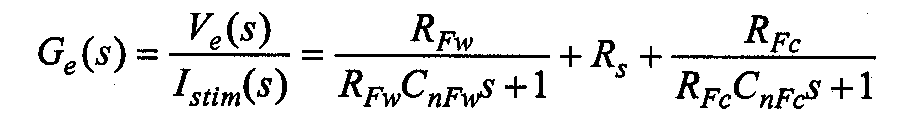
여기서, RFw와 RFc는 각각 작동 전극과 카운터 전극의 패러데이 저항들이고, CnFw와 CnFc는 각각 작동 전극과 카운터 전극의 비페러데이 캐패시터이다. Rs는 전해액의 저항이다. Where R Fw and R Fc are the Faraday resistances of the working and counter electrodes, respectively, and C nFw and C n Fc are non-ferrode capacitors of the working and counter electrodes, respectively. R s is the resistance of the electrolyte.
도 3에 도시된 바와 같이, 본 실시예에 따르면, 전극체(10)는 생체 내 신경(미도시)에 감아져 상기 신경이 표면에 전기 자극을 할 수 있는 커프형 전극체이다. As shown in Fig. 3, according to the present embodiment, the
커프형 전극체(10)는 링 형의 백금 접촉점들을 구비하는 폴리이미드 기판(19)으로 구성된다. 두 개의 단부 접촉점들은 쇼트되어 작동 전극(11, 12)으로 이용되고, 두 개의 중앙 접촉점들은 쇼트되어 카운터 전극(13, 14)으로 이용된다. 폴리이미드 기판(19)은 내부로 말릴 수 있게 구성되어, 신경의 외면에 감아질 수 있다. The cuff-shaped
네 개의 전극(11 내지 14)은 각각 접속 패드(15 내지 18)와 전기적으로 연결된다. 입력되는 전류 펄스의 상에 따라, 전류는 작동 전극을 통해 전도성 매질인 신경을 거쳐 카운터 전극으로 흐른다. The four
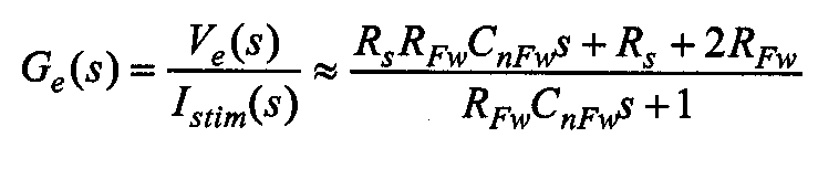
일반적으로, 카운터 전극(13, 14)은 큰 표면적을 가진다. 따라서, 큰 캐패시턴스를 가지는 것으로 고려할 수도 있어 전극 전압에 대한 영향을 무시할 수 있다. 하지만, 본 실시예에 따른 커프형 전극체(10)는, 카운터 전극(13, 14)이 작동 전극(11, 12)의 표면적과 동일 또는 유사한 단면적을 가지도록 형성된다. 따라서, 카운터 전극(13, 14)의 효과가 회로 모델에 포함된다. Generally, the
본 실시예에 따른 작동 전극과 카운터 전극의 패러데이 임피던스와 비패러데이 임피던스는, 전극체(10)를 그가 삽입되는 생체 환경과 유사한 전해액 내부에서 인가된 자극 전류와 그에 따른 전극 전압을 측정함으로써, 사전 결정된다. 실험에 따르면, 작동 전극의 패러데이 저항과 비패러데이 캐패시턴스가 카운터 전극의 패러데이 저항과 비패러데이 캐패시턴스와 유사한 것으로 도출되었다.The Faraday impedance and the non-Faraday impedance of the working electrode and the counter electrode according to this embodiment can be determined by measuring the stimulation current applied in the electrolyte similar to the living environment in which the
따라서, 전극체(10)의 전달함수(Ge(S))는 하기 [수학식 2]와 같이 단순화될 수 있다. Therefore, the transfer function G e (S) of the
[수학식 2]&Quot; (2) "
전압-제어 Voltage-controlled 전류원Current source
본 실시예에 따르면, 전극체(10)로 자극 전류(Istim)을 제공하기 위해 전압-제어 전류원(voltage-controlled current source)(20)이 이용된다. According to the present embodiment, a voltage-controlled
전압-제어 전류원은 출력 임피던스가 현저하게 크고, 출력 전류 에러가 넓은 영역의 자극 주기에 걸쳐 최소화될 필요가 있다. 이를 위해, 본 실시예에 따르면, 도 4에 도시된 바와 같이, 이중 동작 증폭기 전류원이 이용된다. The voltage-controlled current source needs to have a significantly higher output impedance, and the output current error needs to be minimized over a wide range of excitation periods. To this end, according to the present embodiment, as shown in Fig. 4, a dual operation amplifier current source is used.
도 4에 도시된 회로는 능동 피드팩 구조를 기초로 하여, 저항(Rstim)을 통해 강하된 전압이 일정 값을 유지할 수 있게 된다. 자극 전압(Vstim)과 자극 전류(Istim) 사이의 관계는 하기 [수학식 3]과 같다. The circuit shown in Fig. 4 is based on the active feed-pack structure, so that the voltage dropped through the resistor R stim can be maintained at a constant value. The relationship between the stimulation voltage V stim and the stimulation current I stim is expressed by the following equation (3).
[수학식 3]&Quot; (3) "

S/H 유닛S / H unit
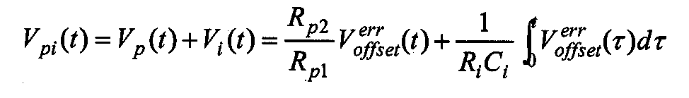
본 명세서의 주요 목적은 전하 밸런싱(balancing) 문제에 대한 피드백 제어 방법을 제공하는 것이다. The main purpose of this specification is to provide a feedback control method for the charge balancing problem.
패드백 루프를 구성하기 위해, 전극 오프셋 전압은 간헐적이 아니라 연속적으로 모니터링되는 것이 바람직하다. To configure the pad back loop, it is preferred that the electrode offset voltage be continuously monitored rather than intermittently.
본 실시예에 따르면, 전극 오프셋 전압을 센싱하기 위해 S/H 방법이 제안된다. According to this embodiment, a S / H method is proposed for sensing the electrode offset voltage.
입력 펄스(Pbb)가 반복 주기를 가지는 2상(biphasic) 펄스로 주어지면, 그와 자극 주기가 동기화된 단상 펄스인 S/H 펄스(Psh)가 S/H 유닛(30))에 인가된다. 그 후, 전극 전압(Ve)은 S/H 펄스(Psh)의 시작점에서 포착되어, S/H 펄스(Psh)의 끝점까지 고정된다. Applied to the input pulse (P bb) are repeated is given by the two-phase (biphasic) pulse having a period, and the stimulus period is the S / H pulse synchronized single-phase pulse (P sh) the S / H unit 30) do. Then, the electrode voltage (V e) is captured at the start of the S / H pulse (P sh), and is fixed to the end of the S / H pulse (P sh).
도 6을 참조하여 다시 설명하면, S/H 유닛(30)은, 입력 펄스(Pbb)가 입력되는 자극 주기에는 입력 펄스(Pbb)의 인가 시점에서 출력된 전극 전압(Ve) 값을 샘플링하고, 샘플링된 전극 전압(Ve) 값을 자극 주기에서의 전극 오프셋 전압(또는, 이하에서는 상황에 따라 "S/H 오프셋 전압"이라고도 표현한다)(Vsh offset) 값으로 고정 출력하고, 입력 펄스(Pbb)가 입력되지 않는 비자극 주기에는 전극체에서 출력되는 전극 전압을 전극 오프셋 전압 값으로 그대로 출력한다. 위와 같은 구성에 따르면, 피드백 제어가 자극 및 비자극 주기 전체에 걸쳐 유지되기 때문에, 자극 주기 동안에 발생하는 전극 오프셋 전압의 변화를 무시할 만하다. 그 결과로, 연속적인 자극에 상관없이, 자극 전류의 간섭을 받지 않고 전극 오프셋 전압을 연속적으로 센싱할 수 있다. Referring to Figure 6 will be described again, S /
도 5에 도시된 바와 같이, S/H 유닛(30)은 아날로그 스위치들과 버퍼들을 이용해 회로가 구성된다. 샘플 모드일 때는, 스위치들이 닫히고, 출력 전압은 입력 전압에 따른다. 홀드 모드에서는, 스위치들이 열리고, 입력 전압은 홀드 캐패시터(Ch)에 의해 고정된다. 페데스탈(pedestal) 에러 및 홀드 타임 글리치(glitch)는 Rc와 Cc의 보상 네크워크에 의해 감소된다. As shown in FIG. 5, the S /
도 6은 샘플 앤 홀드 동작의 일 예를 도시한 것이다. Figure 6 shows an example of a sample and hold operation.
밸런싱되지 않은 2상 전류 펄스가 전극체(10)에 가해지면, 전극 전압(Ve)이 단일 펄스의 끝점에서 없어지지 않으며, 그 오프셋 전압이 연속의 펄스에 의해 점진적으로 증가한다. When the unbalanced two-phase current pulse is applied to the
전극 전압(Ve)은 S/H 펄스의 타이밍에 따라 샘플링되고 고정된다. 그 결과, 샘플 앤 홀드된 전극 오프셋 전압(Vsh offset)은 하기 [수학식 4]와 같이 주어진다. The electrode voltage (V e ) is sampled and fixed according to the timing of the S / H pulse. As a result, the sample and hold electrode offset voltage (V sh offset ) is given by Equation (4) below.
[수학식 4]&Quot; (4) "
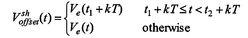
여기서, k = 0, 1, 2,...이고, t1, t2 및 T는 각각 S/H 펄스의 시작 시점, 종료 시점 및 반복 주기이다. Here, k = 0, 1, 2, ..., t 1 , t 2 and T are the start point, end point and repetition period of the S / H pulse, respectively.
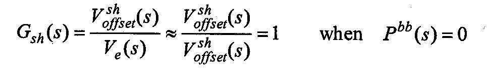
후술하는 바와 같이, PI 제어기가 이용되는 제어기(60)의 설계 과정에서는, 기준 오프셋 전압(Vref offset _)이 스텝 함수로 주어지고, 밸런싱된 2상 입력 펄스(Pbb)가 전압이 전극체(10)에 인가되지 않는 것으로 가정한다. 이는, 제어 목적이 전극 오프셋 전압을 조절하기 위한 것이지 전극 전압(Ve)을 제어하는 것이 아니고, 밸런싱된 밸런싱된 2상 펄스(Pbb)는 외란으로 간주되기 때문이다. 이러한 상황에서, 전극 전압(Ve)은 대략 전극 오프셋 전압(Vsh offset)으로 근사될 수 있다. 따라서, S/H 유닛(30)의 전달함수는 하기 [수학식 5]로 나타낼 수 있다. As will be described later, PI in the design process of the
[수학식 5]&Quot; (5) "
펄스 생성기Pulse generator
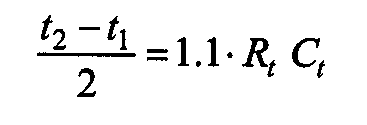
상술한 바와 같이, 2상 펄스인 입력 펄스(Pbb)는 음극 펄스와 양극 펄스로 이루어지고, S/H 펄스는 입력 펄스(Pbb)의 폭과 동일한 폭의 단상 파형을 가진다. 이러한 펄스들은 도 7에 도시된 바와 같은 타이머(T)들과 차동 증폭기들로 이루어진 펄스 생성기(40)에 의해 생성된다. 두 개의 타이머(T)들은 단안정성(monostable) 동작을 수행하도록 시리즈로 형성된다. 도 8은 펄스 생성에 대한 일 예를 도시한 것이다. As described above, the input pulse Pbb as a two-phase pulse is composed of a negative pulse and a positive polarity pulse, and the S / H pulse has a single-phase waveform having the same width as the input pulse Pbb . These pulses are generated by a
음극 펄스(Vcathodic)보다 작은 폭을 가지는 네거티브 트리거 펄스(negative trigger pulse)(Vtrig)가 외부 장치(미도시)에 의해 생성되어 펄스 생성기(40)에 가해진다. 음극 펄스(Vcathodic)는 트리거 펄스(Vtrig)의 폴링 에지(falling edge)로부터 생성되어 하이패스 필터에 연결된다. 양극 펄스(Vanodic)는 상기 하이패스 필터의 출력의 폴링 에지로부터 생성된다. 양극 펄스와 음극 펄스의 폭은 저항(Rt)과 캐피시터(Ct)의 조합에 의해 하기 [수학식 6]과 같이 제어된다. A negative trigger pulse V trig having a width smaller than the cathodic pulse V cathodic is generated by an external device (not shown) and applied to the
[수학식 6]&Quot; (6) "
타이머(T)들로부터의 출력들은 차감 증폭기에 의해 차감되고, 반전된 음극 펄스가 양극 펄스에 더해진다. 출력된 2상 펄스(Pbb)는 진폭 조절을 위해 전압 디바이더(divider)와 전압 팔로어(follower)를 통해 공급된다. The outputs from the timers T are subtracted by the subtracter and the inverted cathode pulses are added to the bipolar pulses. The output two-phase pulse (P bb ) is supplied through a voltage divider and a voltage follower for amplitude control.
또한, S/H 펄스(Psh)가 2상 펄스(Pbb)에 이용된 동일한 양극 펄스와 음극 펄스로 생성된다. 타이머(T)들로부터의 출력들은 반전 합성 증폭기에 의해 더해지고, 그들의 극성이 반전 증폭기에 의해 반전된다. 이러한 회로는, S/H 펄스(Psh)가 2상 펄스(Pbb)에 동기화될 수 있도록 해준다.
Further, the S / H pulse P sh is generated by the same positive polarity pulse and negative polarity pulse used for the two-phase pulse P bb . The outputs from the timers T are added by the inverting synthesis amplifier, and their polarity is inverted by the inverting amplifier. This circuit allows the S / H pulse P sh to be synchronized to the two-phase pulse P bb .
기준 오프셋 전압 생성기Reference offset voltage generator
도 9에 도시된 바와 같이, 기준 오프셋 전압 생성기(50)는 전압 디바이더와 전압 팔로어를 이용해 구성된다. 기준 오프셋 전압(Vref offset)은 전위차계의 세팅에 의해 형성된다. As shown in FIG. 9, the reference offset
도 9의 회로에 따른 기준 오프셋 전압 생성기(50)를 이용하면, 전위차계의 센터 텝의 위치를 바꿔 저항값을 바꿈으로써, 생성되는 기준 오프셋 전압값을 가변할 수 있다. By using the reference offset
예를 들어, 400mV의 기준 오프셋 전압은 VDD와 VSS가 각각 15V와 -15V이고, Roffset이 10kΩ이며, 전위차계(POToffset)의 센터 탭이 10548Ω의 저항을 통해 VSS와 연결됨으로써 얻어질 수 있다.
For example, a reference offset voltage of 400 mV can be obtained by connecting VDD and VSS to 15 V and -15 V, R offset to 10 kΩ, and the center tap of the potentiometer (POT offset ) to VSS through a resistor of 10548 Ω.
제어기Controller
도 1에서 설명되지 않은 부분은 제어기(60)이다. 본 실시예에 따르면, 제어기(60)는 비례적분(PI) 제어기가 이용된다. 1 is a
제어기(60)의 제어 목표는 전극 오프셋 전압(Vsh offset)이 주어진 기준 오프셋 전압(Vref offset)을 추종하도록 하는 것이다. 따라서, 제어기(60)에 입력되는 에러 오프셋 전압(Verr offset)은 하기 [수학식 7]과 같다. The control target of the
[수학식 7]&Quot; (7) "

PI 제어기(60)는 현재 오차(current error)와 시간에 따른 누적 오차에 비례한 제어 신호를 하기 [수학식 8]과 같이 생성한다. The
[수학식 8]&Quot; (8) "
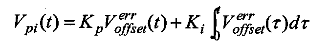
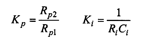
여기서, Kp와 Ki는 각각 비례 이득과 적분 이득이다. Where K p and K i are proportional gain and integral gain, respectively.
그후, 자극 전압(Vstim)은 하기 [수학식 9]와 같이 제어기(60)의 출력인 제어 전압(Vpi)과 입력 펄스(Pbb)의 합성 값으로 출력된다.Thereafter, the excitation voltage V stim is output as a composite value of the control voltage V pi and the input pulse P bb , which are the outputs of the
[수학식 9]&Quot; (9) "
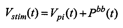
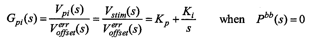
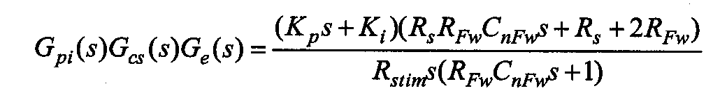
상술한 바와 같이, 제어기의 설계 과정에서는 입력 펄스(Pbb)는 외란으로 간주되어, 전극체(10)에 인가되지 않는 것으로 가정한다. 따라서, 자극 전압(Vstim)은 제어기(60)의 출력과 동일하고, 제어기(60)의 전달함수는 하기 [수학식 10]과 같이 얻을 수 있다. As described above, in the designing process of the controller, it is assumed that the input pulse P bb is regarded as a disturbance and is not applied to the
[수학식 10]&Quot; (10) "
상기 [수학식 2], [수학식 3] 및 [수학식 5]를 이용하면, 전기 자극 시스템(1) 전체에 대한 전달함수 블록도가 도 10과 같이 도시된다. Using the above equations (2), (3) and (5), the transfer function block diagram for the entire
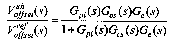
상술한 바와 같이, 샘플 앤 홀드 유닛의 전달함수는 실질적으로 1로 둘 수 있기 때문에, 폐루프(closed-loop) 전달 함수는 하기 [수학식 11]고 같이 도출된다. As described above, since the transfer function of the sample-and-hold unit can be substantially set to 1, a closed-loop transfer function is derived as follows.
[수학식 11]&Quot; (11) "
여기서, 개루프 전달함수는 하기 [수학식 12]와 같다. Here, the open loop transfer function is expressed by Equation (12).
[수학식 12]&Quot; (12) "
전극체(10)의 전하를 밸런싱하기 위해서, 통상 기준 오프셋 전압은 임의의 크기를 가지는 스텝 함수로 주어진다. In order to balance the charge on the
단위 스텝 함수를 가정하고, 제어 성능 사양(the specifications of the control performance)을 다음과 같이 설정한다. Assuming a unit step function, the specifications of the control performance are set as follows.
(1) 정상 상태 에러= 0(1) Steady state error = 0
(2) 최대 오버슈트 ≤ 12%(2) Maximum overshoot ≤ 12%
(3) 라이즈(rise) 타임 ≤ 1.5ms(3) Rise time ≤ 1.5 ms
(4) 세틀링(settling) 타임 ≤ 6ms(4) Settling time ≤ 6 ms
(5) 제어기의 최대 출력 ≤ 1000μA(5) Maximum output of controller ≤ 1000μA
PI 제어기(60)의 즉각적인 효과는 S=0에서 개루프(open-loop) 전달함수에 폴(pole)을 추가하는 것으로 나타난다. 기준 오프셋 전압(Vref offset)이 단위 스텝 함수이면, 정상상태 에러는 하기 [수학식 13]으로 주어진다. The immediate effect of the
[수학식 13]&Quot; (13) "

제어기(60)는 단위 스텝 함수에 대한 정상상태 에러를 0으로 감소시킨다. 따라서, PI 제어기(60)의 디자인 문제는 과도 상태 응답 및 제어기 출력이 주어진 제어 성능 사양 만족하는 비례 이득과 적분 이득을 선택하는 것으로 단순화된다. PI 제어기(60)는 기본적으로 저역 통과 필터이기 때문에, 폐루프 시스템은 항상 더 느린 라이즈 타임과 더 긴 세틀링 타임을 가진다. 하지만, S=-Ki/Kp인 제로의 위치가 적절하게 선택되면, 과도 상태 응답 특성은 개선될 수 있다. 루트 로커스 기술이 PI 제어기(60)를 설계하기 위한 시스템적 방법으로 제안된다. The
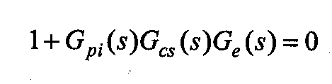
폐루프 시스템의 특성 방정식은 전달함수의 분모 다항식을 0으로 놓음으로써 얻어진다. 따라서, 본 시스템의 특성 방정식의 근은 하기 [수학식 14]를 만족해야 한다. The characteristic equation of the closed-loop system is obtained by setting the denominator polynomial of the transfer function to zero. Therefore, the root of the characteristic equation of the present system should satisfy the following expression (14).
[수학식 14]&Quot; (14) "
특성 방정식의 근은 폐루프 전달함수의 폴에 해당하고, 폐루프 시스템의 안정성 및 과도 상태 응답을 결정한다. PI 이득을 가지는 제어 특성을 평가하기 위하여, 개루프 전달 함수가 곱셈 계수(multiplying factor)로서 가변적인 파라미터 K를 가진다고 가정한다. 따라서, 특성 방정식은 하기 [수학식 15]와 같이 다시 쓸 수 있다. The root of the characteristic equation corresponds to the pole of the closed-loop transfer function, and determines the stability and transient response of the closed-loop system. To evaluate the control characteristic with the PI gain, it is assumed that the open-loop transfer function has a variable parameter K as a multiplying factor. Therefore, the characteristic equation can be rewritten as Equation (15) below.
[수학식 15]&Quot; (15) "
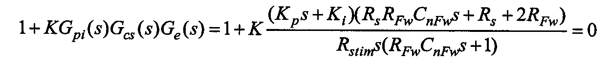
상기 [수학식 15]에서 K=0이면, 개루프 전달함수의 폴이 특성 방정식의 근이 되고, K=∞이면, 개루프 전달함수의 제로가 특성 방정식의 근이 된다는 것은 명백하다. 이러한 루트 로커스 특성은, 적절한 PI 이득을 선택하고, 파라미터 K를 0에서 ∞로 변화시킴에 따른 폐루프 시스템의 제어 형태를 이해하는데 유용하다. If K = 0 in Equation (15), the pole of the open loop transfer function becomes the root of the characteristic equation, and if K = ∞, it is clear that the zero of the open loop transfer function becomes the root of the characteristic equation. This root locus property is useful for understanding the control form of the closed loop system by selecting the appropriate PI gain and changing the parameter K from 0 to ∞.
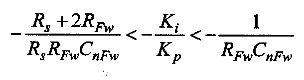
특성 방정식의 모든 근은 선형 제어 시스템의 안정성을 만족하기 위하여, S-평면에서 좌반 평면에 위치하여야 한다. 특성 방정식과 개루프 전달 함수의 관계로부터, S=-Ki/Kp인 제로는 0보다 작은 값으로 선택되어야 한다. 또한, 적분 이득은 적용되는 회로에서 캐패시터 값에 반비례하기 때문에, 적분 이득은 비례 이득보다 큰 값으로 선택되어야 한다. All the roots of the characteristic equation should be located in the left plane of the S-plane in order to satisfy the stability of the linear control system. From the relationship between the characteristic equation and the open-loop transfer function, zero for S = -K i / K p should be chosen to be less than zero. Also, since the integral gain is inversely proportional to the capacitor value in the applied circuit, the integral gain should be chosen to be greater than the proportional gain.
제로의 위치를 선택하기 위하여, 개루프 전달함수의 폴-제로 위치가 도 11과 같이 표시되었다. PI 제어기(60)의 제로를 위치시키기 위한 가능한 구역은 전극체의 폴과 제로의 위치에 의해 분리된다. 수학적인 시뮬레이션 결과는 구역 1에 위치하는 제로는 과도 상태에서 오버 댐프 응답을 제공하고, 구역 3에 위치하는 제로는 정원 공급 전압을 초과하는 큰 제어 출력을 발생시킨다. 따라서, 제로의 위치는 구역 2에 선택되고, 하기 [수학식 16]을 만족한다. To select the position of zero, the pole-zero position of the open loop transfer function is shown as in FIG. A possible area for locating the zero of the
[수학식 16]&Quot; (16) "
도 12는 ki=2000이고, kp=5일 때 K를 0에서 ∞로 변화시킬 때의 특성방적식 [수학식 15]의 루트 로커스 곡선을 도시한다. 12 shows the root locus curve of the characteristic equation (15) when k i = 2000 and k p = 5 when K is changed from 0 to ∞.
여기서, K의 값이 적절히 선택되면, 제어 특성이 향상될 수 있다. 도 13은 도 12의 도시된 몇몇 K 값에 대응하는 PI 제어기의 단위 스탭 응답 및 출력을 도시한 것이다. 도 13을 참조하면, K 값이 증가하면, 과도 상태 응답이 개선되는 것을 알 수 있다. 반면에, 더 큰 제어 출력이 요구됨을 확인할 수 있다. Here, if the value of K is appropriately selected, the control characteristic can be improved. 13 shows the unit step response and output of the PI controller corresponding to the several K values shown in FIG. Referring to FIG. 13, it can be seen that as the value of K increases, the transient response is improved. On the other hand, a larger control output is required.
도 14는 본 실시예에 따른 PI 제어기(60)의 구성을 도시한 것이다. PI 제어기(60)는 비례항과 적분항은 각각 반전 증폭기 및 적분기를 이용해 구현된다. 비례항 및 적분항의 음 이득은 반전 합성 증폭기에 의해 양 이득으로 반전된다. 에러 오프셋 전압(Verr offset)은 차동 증폭기에 의해 생성되고, 그 음 신호는 PI 제어기의 출력 제어 전압(Vpi)을 입력 펄스(Pbb)에 합성하는데 이용되는 추가적인 차동 증폭기에 의해 제거된다. Fig. 14 shows the configuration of the
따라서, PI 제어기(60)의 출력인 제어 전압(Vpi)는 하기 [수학식 17]로 주어진다. Therefore, the control voltage V pi , which is the output of the
[수학식 17]&Quot; (17) "
상기 [수학식 8]과 [수학식 17]을 대비하면, PI 제어기의 파라미터들은 다음 [수학식 18]과 같이 시스템의 파라미터에 관계되는 것을 알 수 있다. Comparing Equations (8) and (17), it can be seen that the parameters of the PI controller are related to the parameters of the system as shown in the following Equation (18).
[수학식 18]&Quot; (18) "
시스템의 동작System behavior
도 15는 기준 오프셋 전압(Vref offset)이 0으로 설정되었을 때, 2상의 입력 펄스에 대한 응답을 도시한 것이다.Fig. 15 shows the response to a two-phase input pulse when the reference offset voltage V ref offset is set to zero.
자극 주기 동안에, 0.5V의 자극 전압(Vstim)이 500μA의 자극 전류(Istim)로 변환된다. 한편, 자극 전류가 인가되는 자극 주기와, 인가되지 않는 비자극 주기 전체에서, S/H 유닛(30)은 자극 전류(Istim)의 간섭을 받지 않고 전극 오프셋 전압(Vsh offset)을 모니터링할 수 있다. During the stimulation period, a stimulation voltage (V stim ) of 0.5V is converted to a stimulation current (I stim ) of 500μA. On the other hand, the entire stimulation period, and is not applied bijageuk period to which the stimulation current, S /
2상 펄스가 전하를 밸런싱하기 위해 설계되지만, 전자 소자의 오차로 인해 발생되는 펄스에는 작은 전하의 불균형이 일어난다. 그 결과로, 전극 전압(Ve)가 각 펄스가 종료된 후에도 사라지지 않고 약 3.2mV의 피크값을 가지는 오프셋 전압이 S/H 회로의 출력에서 관측된다. 이러한 전하 불균형을 보상하기 위하여, PI 제어기(60)는 자극 전류(Istim)을 음으로 변환한 역상의 제어 전압을 발생시키고, 비 자극 주기 동안 오프셋 전압을 0V로 조절한다. Although the two-phase pulse is designed to balance the charge, a small charge imbalance occurs in the pulse generated by the error of the electronic device. As a result, an offset voltage having a peak value of about 3.2 mV is observed at the output of the S / H circuit without the electrode voltage (V e ) disappearing after each pulse ends. To compensate for this charge imbalance, the
도 16은 0이 아닌 기준 오프셋 전압을 설정하였을 때, 2상의 입력 펄스에 대한 응답을 도시한 것이다. 펄스가 인가되기 전의 최초 기간 동안, 기준값과 S/H 유닛(30)에서 출력된 S/H 오프셋 전압 사이의 에러는 PI 제어기(60)에 의해 빠르게 감소한다. 16 shows the response to the input pulse of two phases when a reference offset voltage other than 0 is set. During the initial period before the pulse is applied, the error between the reference value and the S / H offset voltage output from the S /
본 실시예에서는 입력 펄스가 2상일 때를 설명하였지만, 반드시 이에 한정되지는 않는다. 도 17은 기준 오프셋 전압(Vref offset)이 0으로 설정되었을 때, 단상의 입력 펄스에 대한 응답을 도시한 것이다. 도 17을 참조하면, PI 제어기가 양의 자극 전류 부분으로 변환되어, 양극 펄스로 작용하는 역상의 전압을 생성하여, 전하의 축적을 방지하는 것을 확인할 수 있다. In the present embodiment, the case where the input pulse is two-phase has been described, but it is not necessarily limited thereto. Fig. 17 shows the response to a single-phase input pulse when the reference offset voltage V ref offset is set to zero. Referring to FIG. 17, it can be seen that the PI controller is converted into a positive excitation current portion to generate a reverse phase voltage acting as a positive pole pulse, thereby preventing accumulation of charges.
도 18(a)는 S/H 유닛(30)에 의한 S/H 동작이 이루어지지 않고, 기준 오프셋 전압이 0일 때 2상의 입력 펄스에 대한 응답을 도시한 것이다. S/H 동작이 이루어지지 않으므로, S/H 유닛(30)의 출력은 전극 전압(Ve)과 동일하다. 자극 주기 동안, 에러 오프셋 전압이 현저한 피크 대 피크 변화를 일으키고, 대응하는 제어기의 출력은 자극 전류에 영향을 준다. 이러한 영향은 S/H 동작이 이루어지는 경우와 비교하여, 비자극 주기 동안 전극 전압이 증가하는 효과를 가져온다. 18 (a) shows a response to a 2-phase input pulse when the S /
신경 멤브레인의 탈분극화와 역 전기화학적 과정은 가해지는 전류에 관계되기 때문에, 전기 자극 시스템에서 자극 전류가 펄스 전체에 걸쳐 일정한 것이 중요하다. 도 18(b)에 도시된 바와 같이, S/H 유닛(30)에 의해 자극 주기 동안, 전극 전압이 고정되고, 자극 전류는 제어기의 출력에 의해 영향받지 않는다. 또한, 비자극 주기 동안에, 전극 전압은 S/H 유닛(30)에 의해 그대로 출력되기 때문에, 그 값은 0의 기준 오프셋 전압을 향해 빠르게 제어된다.
Since the depolarization and reverse electrochemical processes of neural membranes are related to the current applied, it is important that the stimulation current is constant throughout the pulse in the electrical stimulation system. As shown in Fig. 18 (b), the electrode voltage is fixed by the S /
본 실시예에 따르면, 샘플 앤 홀드 유닛이 예를 들어, 자극 전류가 인가되는 시점에서 출력된 전극 전압 값을 포착하고, 포착된 전극 전압 값을 상기 자극 전류의 인가되는 동안의 전극 오프셋 전압 값으로서 고정하여 출력하므로, 자극 전류의 간섭을 받지 않고 전극 오프셋 전압을 지속적으로 모니터링할 수 있다. According to the present embodiment, the sample and hold unit captures the electrode voltage value output at the time when the stimulus current is applied, for example, and detects the electrode voltage value as the electrode offset voltage value during application of the stimulus current So that it is possible to continuously monitor the electrode offset voltage without being interfered with the stimulation current.
비자극 주기 동안의 전극 오프셋 전압은 PI 제어기로 피드백되고, 자극 주기 동안에 전극 오프셋 전압의 변화는 무시할 수 있다. 따라서, S/H 유닛의 시스템적 전달함수는 1로 설정 가능하여, PI 제어기의 제어 이득을 설계함에 있어 시스템을 간소화할 수 있다. The electrode offset voltage during the non-stimulation period is fed back to the PI controller, and the change in electrode offset voltage during the stimulation period can be ignored. Therefore, the system transfer function of the S / H unit can be set to 1, which simplifies the system in designing the control gain of the PI controller.
본 실시예에 따는 전극체는 전극-전해질 모델을 기반으로 하고, 전해액에서의 사전 실험을 통해 그 임피던스 값이 결정되어 있으므로, PI 제어기의 설계에 필요한 변수를 알아내기 위한 노력이 크게 감소한다. Since the electrode body according to this embodiment is based on the electrode-electrolyte model and the impedance value is determined through the preliminary experiment in the electrolytic solution, efforts for finding the parameters required for the design of the PI controller are greatly reduced.
Claims (15)
자극 전류를 전도성 매질에 인가하는 전극체;
입력 펄스를 이용해 상기 자극 전류를 생성하여 상기 전극체에 입력하는 자극 전류 생성 유닛;
상기 전극체에서 출력되는 전극 전압에서 전극 오프셋 전압을 분류하여 출력하는 샘플 앤 홀드 유닛;
기설정된 기준 오프셋 전압과 상기 전극 오프셋 전압의 에러를 최소화하기 위한 제어 신호를 출력하는 제어기를 포함하고,
상기 샘플 앤 홀드 유닛은,
상기 입력 펄스가 인가되면 상기 입력 펄스의 인가 시점에서 출력된 전극 전압 값을 샘플링하고, 샘플링된 전극 전압 값을 자극 주기에서의 전극 오프셋 전압 값으로 고정 출력하고,
상기 샘플 앤 홀드 유닛에서 출력된 전극 오프셋 전압은 상기 제어기로 피드백되고,
상기 자극 전류 생성 유닛은 상기 제어 신호를 반영한 상기 자극 전류를 생성하여 상기 전극체에 전달하는 것을 특징으로 하는 전기 자극 시스템.An electric stimulation system using an electrode body,
An electrode body for applying a stimulating current to the conductive medium;
A stimulating current generating unit that generates the stimulating current using an input pulse and inputs the generated stimulating current to the electrode body;
A sample and hold unit for classifying and outputting an electrode offset voltage at an electrode voltage output from the electrode body;
And a controller for outputting a control signal for minimizing an error of the predetermined reference offset voltage and the electrode offset voltage,
The sample and hold unit includes:
Wherein when the input pulse is applied, the electrode voltage value output at the application time of the input pulse is sampled, the sampled electrode voltage value is fixedly output as the electrode offset voltage value in the stimulus period,
The electrode offset voltage output from the sample and hold unit is fed back to the controller,
Wherein the stimulating current generating unit generates the stimulating current reflecting the control signal and transmits the generated stimulating current to the electrode body.
상기 제어기는 상기 제어 신호로 제어 전압을 출력하고,
상기 자극 전류 생성 유닛은,
입력 펄스를 생성하는 펄스 생성기;
상기 입력 펄스와 상기 제어 전압이 합성된 자극 전압을 상기 자극 전류로 변환하여 상기 전극체에 전달하는 전압-제어 전류원을 포함하는 것을 특징으로 하는 전기 자극 시스템. The method according to claim 1,
The controller outputs a control voltage with the control signal,
The stimulus current generating unit includes:
A pulse generator for generating an input pulse;
And a voltage-controlled current source for converting a stimulation voltage obtained by synthesizing the input pulse and the control voltage into the stimulation current and delivering the stimulation current to the electrode body.
상기 입력 펄스는 일정한 주기의 펄스로 인가되고,
상기 자극 전압 및 상기 자극 전류는 상기 입력 펄스와 동일 주기의 펄스로 출력되는 것을 특징으로 하는 전기 자극 시스템. The method of claim 3,
The input pulse is applied with a pulse of a constant period,
Wherein the stimulation voltage and the stimulation current are output in pulses having the same period as the input pulse.
상기 펄스 생성기는,
상기 입력 펄스와 동기화된 샘플 앤 홀드 펄스를 생성하여 상기 샘플 앤 홀드 유닛으로 입력하고,
상기 샘플 앤 홀드 유닛은,
상기 샘플 앤 홀드 펄스가 인가되지 않는 동안에는 상기 전극체에서 출력되는 전극 전압을 그대로 상기 전극 오프셋 전압으로 출력하도록 구성된 것을 특징으로 하는 전기 자극 시스템. 5. The method of claim 4,
Wherein the pulse generator comprises:
A sample and hold pulse synchronized with the input pulse is generated and input to the sample and hold unit,
The sample and hold unit includes:
And outputs the electrode voltage output from the electrode body as the electrode offset voltage while the sample and hold pulse is not applied.
상기 입력 펄스는 음극 펄스와 양극 펄스로 구성된 2상 펄스로 생성되는 것을 특징으로 전기 자극 시스템. 6. The method of claim 5,
Wherein the input pulse is generated as a two-phase pulse consisting of a negative pulse and a positive pulse.
상기 샘플 앤 홀드 펄스는 단상 펄스로 생성되는 것을 특징으로 하는 전기 자극 시스템. The method according to claim 6,
Wherein the sample and hold pulse is generated as a single phase pulse.
상기 전극체는 상기 자극 전류가 입력되는 작동 전극과, 상기 자극 전류가 출력되는 카운터 전극을 포함하는 것을 특징으로 하는 전기 자극 시스템.The method according to claim 1,
Wherein the electrode body includes a working electrode to which the magnetic pole current is inputted and a counter electrode to which the magnetic pole current is outputted.
상기 카운터 전극의 표면적은 상기 작동 전극의 표면적과 동일 또는 유사한 것을 특징으로 하는 전기 자극 시스템. 9. The method of claim 8,
Wherein the surface area of the counter electrode is the same as or similar to the surface area of the working electrode.
상기 전도성 매질은 생물의 신경이고,
상기 전극체는 상기 신경에 부착되어 상기 신경에 전기 자극을 전달하는 것을 특징으로 하는 전기 자극 시스템. 10. The method of claim 9,
The conductive medium is a nerve of the organism,
Wherein the electrode body is attached to the nerve to transmit an electrical stimulus to the nerve.
상기 전극체는 전해질 내부에서 패러데이 임피던스와 비패러데이 임피던스가 병렬 연결되는 회로 모델로 모델링되고,
상기 패러데이 임피던스와 비패러데이 임피던스는 상기 전극체를 상기 생물의 생체 환경과 유사한 전해질 실험을 통해 사전 결정된 것을 특징으로 하는 전기 자극 시스템. 11. The method of claim 10,
The electrode body is modeled as a circuit model in which a Faraday impedance and a non-Faraday impedance are connected in parallel within the electrolyte,
Wherein the Faraday impedance and the non-Faraday impedance are predetermined through an electrolyte experiment similar to the biological environment of the organism.
상기 전극체는 상기 신경에 감아져 상기 신경이 표면에 전기 자극을 할 수 있는 커프형 전극체인 것을 특징으로 하는 전기 자극 시스템. 11. The method of claim 10,
Wherein the electrode body is a cuff-shaped electrode wound around the nerve and capable of causing electrical stimulation to the surface of the nerve.
상기 제어기는 비례 적분 제어기인 것을 특징으로 하는 전기 자극 시스템. The method according to claim 1,
Wherein the controller is a proportional integral controller.
상기 비례 적분 제어기의 제어 이득은,
상기 샘플 앤 홀드 유닛의 전달함수를 1로 설정하여 결정되는 것을 특징으로 하는 전기 자극 시스템. 14. The method of claim 13,
The control gain of the proportional-plus-
And the transfer function of the sample-and-hold unit is set to 1.
상기 기준 오프셋 전압을 가변적으로 생성할 수 있는 기준 오프셋 전압 생성기를 더 포함하는 것을 특징으로 하는 전기 자극 시스템. The method according to claim 1,
Further comprising a reference offset voltage generator capable of variably generating the reference offset voltage.
Priority Applications (1)
| Application Number | Priority Date | Filing Date | Title |
|---|---|---|---|
| KR20130079828A KR101508158B1 (en) | 2013-07-08 | 2013-07-08 | Control of electrical offset volage in Functional Electrical Stimulation system |
Applications Claiming Priority (1)
| Application Number | Priority Date | Filing Date | Title |
|---|---|---|---|
| KR20130079828A KR101508158B1 (en) | 2013-07-08 | 2013-07-08 | Control of electrical offset volage in Functional Electrical Stimulation system |
Publications (2)
| Publication Number | Publication Date |
|---|---|
| KR20150006256A KR20150006256A (en) | 2015-01-16 |
| KR101508158B1 true KR101508158B1 (en) | 2015-04-07 |
Family
ID=52569706
Family Applications (1)
| Application Number | Title | Priority Date | Filing Date |
|---|---|---|---|
| KR20130079828A Expired - Fee Related KR101508158B1 (en) | 2013-07-08 | 2013-07-08 | Control of electrical offset volage in Functional Electrical Stimulation system |
Country Status (1)
| Country | Link |
|---|---|
| KR (1) | KR101508158B1 (en) |
Families Citing this family (2)
| Publication number | Priority date | Publication date | Assignee | Title |
|---|---|---|---|---|
| KR102897303B1 (en) * | 2018-10-26 | 2025-12-10 | 모나쉬 유니버시티 | Systems and methods for monitoring neural activity |
| KR102768808B1 (en) * | 2022-08-18 | 2025-02-19 | 전북대학교산학협력단 | Microcurrent treatment device |
Citations (4)
| Publication number | Priority date | Publication date | Assignee | Title |
|---|---|---|---|---|
| JPH059515U (en) * | 1991-07-18 | 1993-02-09 | 横河メデイカルシステム株式会社 | DC correction device for digital phasing adder |
| KR20050042481A (en) * | 2002-08-20 | 2005-05-09 | 나노겐 인코포레이티드 | Programmable multiplexed active biologic array |
| JP2009545188A (en) | 2006-03-21 | 2009-12-17 | ケンブリッジ アナログ テクノロジー,エルエルシー | Cancel offset of sample data circuit |
| JP2012520730A (en) | 2009-03-16 | 2012-09-10 | ニューロスキー・インコーポレーテッド | EEG control of devices using sensory evoked potentials |
-
2013
- 2013-07-08 KR KR20130079828A patent/KR101508158B1/en not_active Expired - Fee Related
Patent Citations (4)
| Publication number | Priority date | Publication date | Assignee | Title |
|---|---|---|---|---|
| JPH059515U (en) * | 1991-07-18 | 1993-02-09 | 横河メデイカルシステム株式会社 | DC correction device for digital phasing adder |
| KR20050042481A (en) * | 2002-08-20 | 2005-05-09 | 나노겐 인코포레이티드 | Programmable multiplexed active biologic array |
| JP2009545188A (en) | 2006-03-21 | 2009-12-17 | ケンブリッジ アナログ テクノロジー,エルエルシー | Cancel offset of sample data circuit |
| JP2012520730A (en) | 2009-03-16 | 2012-09-10 | ニューロスキー・インコーポレーテッド | EEG control of devices using sensory evoked potentials |
Also Published As
| Publication number | Publication date |
|---|---|
| KR20150006256A (en) | 2015-01-16 |
Similar Documents
| Publication | Publication Date | Title |
|---|---|---|
| US12383744B2 (en) | Circuitry to assist with neural sensing in an implantable stimulator device | |
| Sooksood et al. | An active approach for charge balancing in functional electrical stimulation | |
| EP3216489B1 (en) | Systems and methods for automated charge balancing of multiple electrodes for uninterrupted therapy and evoked response sensing | |
| US8788032B2 (en) | Method and circuitry for measurement of stimulation current | |
| US10363423B2 (en) | Pulse-by-pulse compliance voltage generation for an implantable stimulator | |
| US20240058611A1 (en) | Using Stimulation Circuitry to Provide DC Offset Compensation at Inputs to Sense Amp Circuitry in a Stimulator Device | |
| Schuettler et al. | A voltage-controlled current source with regulated electrode bias-voltage for safe neural stimulation | |
| Boretius et al. | On the stability of poly‐ethylenedioxythiopene as coating material for active neural implants | |
| Lo et al. | Precision control of pulse widths for charge balancing in functional electrical stimulation | |
| KR101508158B1 (en) | Control of electrical offset volage in Functional Electrical Stimulation system | |
| Cui et al. | A 3-mV precision dual-mode-controlled fast charge balancing for implantable biphasic neural stimulators | |
| AU2021277095A1 (en) | Neural recording with stimulus crosstalk compensation | |
| WO2021158308A1 (en) | Parametric characterization of an implanted stimulation lead system associated with an implantable pulse generator | |
| Krishnan et al. | On the cause and control of residual voltage generated by electrical stimulation of neural tissue | |
| Sooksood et al. | Recent advances in charge balancing for functional electrical stimulation | |
| US8588928B2 (en) | Active electrode state control system with current compensation to reduce residual DC/LF voltage | |
| Ranjandish et al. | An active charge balancing method based on self-oscillation of the anodic current | |
| Ranjandish et al. | A fully fail-safe capacitive-based charge metering method for active charge balancing in deep brain stimulation | |
| Chu et al. | Feedback control of electrode offset voltage during functional electrical stimulation | |
| Hung et al. | Pulse-clamp technique for characterizing neural-stimulating electrodes | |
| Shulyzki et al. | CMOS current-copying neural stimulator with OTA-sharing | |
| Ou et al. | Electronics for a safe direct current stimulator | |
| Tang et al. | A Biphasic Neural Stimulator with Adaptive Pulse-Width Modulation Charge Balancer | |
| Ranjandish et al. | Polarity detection base pulse insertion for active charge balancing in electrical stimulation | |
| US9694182B2 (en) | Devices for electrical stimulation of a biological tissue and method for calibrating same |
Legal Events
| Date | Code | Title | Description |
|---|---|---|---|
| A201 | Request for examination | ||
| PA0109 | Patent application |
St.27 status event code: A-0-1-A10-A12-nap-PA0109 |
|
| PA0201 | Request for examination |
St.27 status event code: A-1-2-D10-D11-exm-PA0201 |
|
| PN2301 | Change of applicant |
St.27 status event code: A-3-3-R10-R13-asn-PN2301 St.27 status event code: A-3-3-R10-R11-asn-PN2301 |
|
| D13-X000 | Search requested |
St.27 status event code: A-1-2-D10-D13-srh-X000 |
|
| D14-X000 | Search report completed |
St.27 status event code: A-1-2-D10-D14-srh-X000 |
|
| E902 | Notification of reason for refusal | ||
| PE0902 | Notice of grounds for rejection |
St.27 status event code: A-1-2-D10-D21-exm-PE0902 |
|
| E13-X000 | Pre-grant limitation requested |
St.27 status event code: A-2-3-E10-E13-lim-X000 |
|
| P11-X000 | Amendment of application requested |
St.27 status event code: A-2-2-P10-P11-nap-X000 |
|
| P13-X000 | Application amended |
St.27 status event code: A-2-2-P10-P13-nap-X000 |
|
| PG1501 | Laying open of application |
St.27 status event code: A-1-1-Q10-Q12-nap-PG1501 |
|
| E701 | Decision to grant or registration of patent right | ||
| PE0701 | Decision of registration |
St.27 status event code: A-1-2-D10-D22-exm-PE0701 |
|
| PR0701 | Registration of establishment |
St.27 status event code: A-2-4-F10-F11-exm-PR0701 |
|
| PR1002 | Payment of registration fee |
St.27 status event code: A-2-2-U10-U11-oth-PR1002 Fee payment year number: 1 |
|
| PG1601 | Publication of registration |
St.27 status event code: A-4-4-Q10-Q13-nap-PG1601 |
|
| P22-X000 | Classification modified |
St.27 status event code: A-4-4-P10-P22-nap-X000 |
|
| FPAY | Annual fee payment |
Payment date: 20180302 Year of fee payment: 4 |
|
| PR1001 | Payment of annual fee |
St.27 status event code: A-4-4-U10-U11-oth-PR1001 Fee payment year number: 4 |
|
| FPAY | Annual fee payment |
Payment date: 20190226 Year of fee payment: 5 |
|
| PR1001 | Payment of annual fee |
St.27 status event code: A-4-4-U10-U11-oth-PR1001 Fee payment year number: 5 |
|
| FPAY | Annual fee payment |
Payment date: 20200302 Year of fee payment: 6 |
|
| PR1001 | Payment of annual fee |
St.27 status event code: A-4-4-U10-U11-oth-PR1001 Fee payment year number: 6 |
|
| PC1903 | Unpaid annual fee |
St.27 status event code: A-4-4-U10-U13-oth-PC1903 Not in force date: 20210328 Payment event data comment text: Termination Category : DEFAULT_OF_REGISTRATION_FEE |
|
| PC1903 | Unpaid annual fee |
St.27 status event code: N-4-6-H10-H13-oth-PC1903 Ip right cessation event data comment text: Termination Category : DEFAULT_OF_REGISTRATION_FEE Not in force date: 20210328 |
|
| PN2301 | Change of applicant |
St.27 status event code: A-5-5-R10-R13-asn-PN2301 St.27 status event code: A-5-5-R10-R11-asn-PN2301 |