KR101503986B1 - Organic light emitting device - Google Patents
Organic light emitting device Download PDFInfo
- Publication number
- KR101503986B1 KR101503986B1 KR1020127017690A KR20127017690A KR101503986B1 KR 101503986 B1 KR101503986 B1 KR 101503986B1 KR 1020127017690 A KR1020127017690 A KR 1020127017690A KR 20127017690 A KR20127017690 A KR 20127017690A KR 101503986 B1 KR101503986 B1 KR 101503986B1
- Authority
- KR
- South Korea
- Prior art keywords
- light emitting
- organic
- layer
- compound
- group
- Prior art date
- Legal status (The legal status is an assumption and is not a legal conclusion. Google has not performed a legal analysis and makes no representation as to the accuracy of the status listed.)
- Active
Links
- 150000002894 organic compounds Chemical class 0.000 claims abstract description 88
- 150000005839 radical cations Chemical class 0.000 claims abstract description 48
- 238000000862 absorption spectrum Methods 0.000 claims abstract description 29
- 239000000463 material Substances 0.000 claims abstract description 28
- 230000005525 hole transport Effects 0.000 claims abstract description 25
- 125000003118 aryl group Chemical group 0.000 claims description 8
- 125000000217 alkyl group Chemical group 0.000 claims description 7
- 125000005843 halogen group Chemical group 0.000 claims description 7
- 125000001997 phenyl group Chemical group [H]C1=C([H])C([H])=C(*)C([H])=C1[H] 0.000 claims description 6
- 125000004435 hydrogen atom Chemical group [H]* 0.000 claims description 5
- 108091008695 photoreceptors Proteins 0.000 claims 1
- 150000001875 compounds Chemical class 0.000 abstract description 54
- 239000010410 layer Substances 0.000 description 158
- YXFVVABEGXRONW-UHFFFAOYSA-N Toluene Chemical compound CC1=CC=CC=C1 YXFVVABEGXRONW-UHFFFAOYSA-N 0.000 description 75
- 238000006243 chemical reaction Methods 0.000 description 67
- 239000000243 solution Substances 0.000 description 47
- 239000002904 solvent Substances 0.000 description 34
- -1 acetoxy phenanthryl Chemical group 0.000 description 29
- 239000012043 crude product Substances 0.000 description 22
- 239000000758 substrate Substances 0.000 description 21
- 229940125782 compound 2 Drugs 0.000 description 19
- IMNFDUFMRHMDMM-UHFFFAOYSA-N N-Heptane Chemical compound CCCCCCC IMNFDUFMRHMDMM-UHFFFAOYSA-N 0.000 description 18
- 239000012044 organic layer Substances 0.000 description 18
- 239000010409 thin film Substances 0.000 description 18
- 230000015572 biosynthetic process Effects 0.000 description 17
- 238000003786 synthesis reaction Methods 0.000 description 17
- 229940125904 compound 1 Drugs 0.000 description 16
- 230000008859 change Effects 0.000 description 15
- 239000003153 chemical reaction reagent Substances 0.000 description 14
- 230000007935 neutral effect Effects 0.000 description 14
- 238000010521 absorption reaction Methods 0.000 description 13
- 239000000470 constituent Substances 0.000 description 13
- XLYOFNOQVPJJNP-UHFFFAOYSA-N water Substances O XLYOFNOQVPJJNP-UHFFFAOYSA-N 0.000 description 13
- 229940126214 compound 3 Drugs 0.000 description 12
- VLKZOEOYAKHREP-UHFFFAOYSA-N n-Hexane Chemical compound CCCCCC VLKZOEOYAKHREP-UHFFFAOYSA-N 0.000 description 12
- 238000010898 silica gel chromatography Methods 0.000 description 11
- HEDRZPFGACZZDS-UHFFFAOYSA-N Chloroform Chemical compound ClC(Cl)Cl HEDRZPFGACZZDS-UHFFFAOYSA-N 0.000 description 10
- 238000000034 method Methods 0.000 description 10
- 239000012299 nitrogen atmosphere Substances 0.000 description 10
- XEKOWRVHYACXOJ-UHFFFAOYSA-N Ethyl acetate Chemical compound CCOC(C)=O XEKOWRVHYACXOJ-UHFFFAOYSA-N 0.000 description 9
- KFZMGEQAYNKOFK-UHFFFAOYSA-N Isopropanol Chemical compound CC(C)O KFZMGEQAYNKOFK-UHFFFAOYSA-N 0.000 description 9
- PMZURENOXWZQFD-UHFFFAOYSA-L Sodium Sulfate Chemical compound [Na+].[Na+].[O-]S([O-])(=O)=O PMZURENOXWZQFD-UHFFFAOYSA-L 0.000 description 9
- 238000005259 measurement Methods 0.000 description 9
- 239000012046 mixed solvent Substances 0.000 description 9
- XKRFYHLGVUSROY-UHFFFAOYSA-N Argon Chemical compound [Ar] XKRFYHLGVUSROY-UHFFFAOYSA-N 0.000 description 8
- LFQSCWFLJHTTHZ-UHFFFAOYSA-N Ethanol Chemical compound CCO LFQSCWFLJHTTHZ-UHFFFAOYSA-N 0.000 description 8
- CTQNGGLPUBDAKN-UHFFFAOYSA-N O-Xylene Chemical compound CC1=CC=CC=C1C CTQNGGLPUBDAKN-UHFFFAOYSA-N 0.000 description 8
- NFHFRUOZVGFOOS-UHFFFAOYSA-N palladium;triphenylphosphane Chemical compound [Pd].C1=CC=CC=C1P(C=1C=CC=CC=1)C1=CC=CC=C1.C1=CC=CC=C1P(C=1C=CC=CC=1)C1=CC=CC=C1.C1=CC=CC=C1P(C=1C=CC=CC=1)C1=CC=CC=C1.C1=CC=CC=C1P(C=1C=CC=CC=1)C1=CC=CC=C1 NFHFRUOZVGFOOS-UHFFFAOYSA-N 0.000 description 8
- MFRIHAYPQRLWNB-UHFFFAOYSA-N sodium tert-butoxide Chemical compound [Na+].CC(C)(C)[O-] MFRIHAYPQRLWNB-UHFFFAOYSA-N 0.000 description 8
- 238000000638 solvent extraction Methods 0.000 description 8
- 239000008096 xylene Substances 0.000 description 8
- CDBYLPFSWZWCQE-UHFFFAOYSA-L Sodium Carbonate Chemical compound [Na+].[Na+].[O-]C([O-])=O CDBYLPFSWZWCQE-UHFFFAOYSA-L 0.000 description 7
- 238000000151 deposition Methods 0.000 description 7
- 230000008021 deposition Effects 0.000 description 7
- 125000006038 hexenyl group Chemical group 0.000 description 7
- 238000003756 stirring Methods 0.000 description 7
- BWHDROKFUHTORW-UHFFFAOYSA-N tritert-butylphosphane Chemical compound CC(C)(C)P(C(C)(C)C)C(C)(C)C BWHDROKFUHTORW-UHFFFAOYSA-N 0.000 description 7
- 238000005160 1H NMR spectroscopy Methods 0.000 description 6
- IJGRMHOSHXDMSA-UHFFFAOYSA-N Atomic nitrogen Chemical compound N#N IJGRMHOSHXDMSA-UHFFFAOYSA-N 0.000 description 6
- SFHYNDMGZXWXBU-LIMNOBDPSA-N 6-amino-2-[[(e)-(3-formylphenyl)methylideneamino]carbamoylamino]-1,3-dioxobenzo[de]isoquinoline-5,8-disulfonic acid Chemical compound O=C1C(C2=3)=CC(S(O)(=O)=O)=CC=3C(N)=C(S(O)(=O)=O)C=C2C(=O)N1NC(=O)N\N=C\C1=CC=CC(C=O)=C1 SFHYNDMGZXWXBU-LIMNOBDPSA-N 0.000 description 5
- 239000007983 Tris buffer Substances 0.000 description 5
- 125000005466 alkylenyl group Chemical group 0.000 description 5
- 239000013078 crystal Substances 0.000 description 5
- 238000010586 diagram Methods 0.000 description 5
- 230000005281 excited state Effects 0.000 description 5
- 239000011521 glass Substances 0.000 description 5
- 238000002347 injection Methods 0.000 description 5
- 239000007924 injection Substances 0.000 description 5
- 238000001840 matrix-assisted laser desorption--ionisation time-of-flight mass spectrometry Methods 0.000 description 5
- 238000002156 mixing Methods 0.000 description 5
- 238000012546 transfer Methods 0.000 description 5
- ZHQNDEHZACHHTA-UHFFFAOYSA-N 9,9-dimethylfluorene Chemical compound C1=CC=C2C(C)(C)C3=CC=CC=C3C2=C1 ZHQNDEHZACHHTA-UHFFFAOYSA-N 0.000 description 4
- 229910045601 alloy Inorganic materials 0.000 description 4
- 239000000956 alloy Substances 0.000 description 4
- 125000005428 anthryl group Chemical group [H]C1=C([H])C([H])=C2C([H])=C3C(*)=C([H])C([H])=C([H])C3=C([H])C2=C1[H] 0.000 description 4
- 229910052786 argon Inorganic materials 0.000 description 4
- 230000008033 biological extinction Effects 0.000 description 4
- 230000000903 blocking effect Effects 0.000 description 4
- 125000000113 cyclohexyl group Chemical group [H]C1([H])C([H])([H])C([H])([H])C([H])(*)C([H])([H])C1([H])[H] 0.000 description 4
- 239000002019 doping agent Substances 0.000 description 4
- 230000005284 excitation Effects 0.000 description 4
- 238000010438 heat treatment Methods 0.000 description 4
- 238000004770 highest occupied molecular orbital Methods 0.000 description 4
- 238000005424 photoluminescence Methods 0.000 description 4
- 230000002265 prevention Effects 0.000 description 4
- 239000007787 solid Substances 0.000 description 4
- 239000000126 substance Substances 0.000 description 4
- WTAPZWXVSZMMDG-UHFFFAOYSA-N 1,5-diphenylpenta-1,4-dien-3-one;palladium Chemical compound [Pd].C=1C=CC=CC=1C=CC(=O)C=CC1=CC=CC=C1 WTAPZWXVSZMMDG-UHFFFAOYSA-N 0.000 description 3
- YMWUJEATGCHHMB-UHFFFAOYSA-N Dichloromethane Chemical compound ClCCl YMWUJEATGCHHMB-UHFFFAOYSA-N 0.000 description 3
- ZMANZCXQSJIPKH-UHFFFAOYSA-N Triethylamine Chemical compound CCN(CC)CC ZMANZCXQSJIPKH-UHFFFAOYSA-N 0.000 description 3
- 229910052782 aluminium Inorganic materials 0.000 description 3
- XAGFODPZIPBFFR-UHFFFAOYSA-N aluminium Chemical compound [Al] XAGFODPZIPBFFR-UHFFFAOYSA-N 0.000 description 3
- 239000007864 aqueous solution Substances 0.000 description 3
- 150000004982 aromatic amines Chemical group 0.000 description 3
- 230000000052 comparative effect Effects 0.000 description 3
- 230000007423 decrease Effects 0.000 description 3
- 238000003795 desorption Methods 0.000 description 3
- 239000011159 matrix material Substances 0.000 description 3
- 239000011259 mixed solution Substances 0.000 description 3
- 229910052757 nitrogen Inorganic materials 0.000 description 3
- 230000001681 protective effect Effects 0.000 description 3
- 125000001725 pyrenyl group Chemical group 0.000 description 3
- 230000009467 reduction Effects 0.000 description 3
- 229910000029 sodium carbonate Inorganic materials 0.000 description 3
- 238000001228 spectrum Methods 0.000 description 3
- RFFLAFLAYFXFSW-UHFFFAOYSA-N 1,2-dichlorobenzene Chemical compound ClC1=CC=CC=C1Cl RFFLAFLAYFXFSW-UHFFFAOYSA-N 0.000 description 2
- YJTKZCDBKVTVBY-UHFFFAOYSA-N 1,3-Diphenylbenzene Chemical group C1=CC=CC=C1C1=CC=CC(C=2C=CC=CC=2)=C1 YJTKZCDBKVTVBY-UHFFFAOYSA-N 0.000 description 2
- 125000000590 4-methylphenyl group Chemical group [H]C1=C([H])C(=C([H])C([H])=C1*)C([H])([H])[H] 0.000 description 2
- CSCPPACGZOOCGX-UHFFFAOYSA-N Acetone Chemical compound CC(C)=O CSCPPACGZOOCGX-UHFFFAOYSA-N 0.000 description 2
- WKBOTKDWSSQWDR-UHFFFAOYSA-N Bromine atom Chemical compound [Br] WKBOTKDWSSQWDR-UHFFFAOYSA-N 0.000 description 2
- CSNNHWWHGAXBCP-UHFFFAOYSA-L Magnesium sulfate Chemical compound [Mg+2].[O-][S+2]([O-])([O-])[O-] CSNNHWWHGAXBCP-UHFFFAOYSA-L 0.000 description 2
- KDLHZDBZIXYQEI-UHFFFAOYSA-N Palladium Chemical compound [Pd] KDLHZDBZIXYQEI-UHFFFAOYSA-N 0.000 description 2
- 125000004054 acenaphthylenyl group Chemical group C1(=CC2=CC=CC3=CC=CC1=C23)* 0.000 description 2
- 239000000853 adhesive Substances 0.000 description 2
- 230000001070 adhesive effect Effects 0.000 description 2
- VSCWAEJMTAWNJL-UHFFFAOYSA-K aluminium trichloride Chemical compound Cl[Al](Cl)Cl VSCWAEJMTAWNJL-UHFFFAOYSA-K 0.000 description 2
- 239000008280 blood Substances 0.000 description 2
- 210000004369 blood Anatomy 0.000 description 2
- GDTBXPJZTBHREO-UHFFFAOYSA-N bromine Substances BrBr GDTBXPJZTBHREO-UHFFFAOYSA-N 0.000 description 2
- 229910052794 bromium Inorganic materials 0.000 description 2
- 230000015556 catabolic process Effects 0.000 description 2
- 150000001768 cations Chemical group 0.000 description 2
- 239000002800 charge carrier Substances 0.000 description 2
- 238000006731 degradation reaction Methods 0.000 description 2
- 125000001495 ethyl group Chemical group [H]C([H])([H])C([H])([H])* 0.000 description 2
- 239000010408 film Substances 0.000 description 2
- 125000003983 fluorenyl group Chemical group C1(=CC=CC=2C3=CC=CC=C3CC12)* 0.000 description 2
- AMGQUBHHOARCQH-UHFFFAOYSA-N indium;oxotin Chemical compound [In].[Sn]=O AMGQUBHHOARCQH-UHFFFAOYSA-N 0.000 description 2
- AFRJJFRNGGLMDW-UHFFFAOYSA-N lithium amide Chemical compound [Li+].[NH2-] AFRJJFRNGGLMDW-UHFFFAOYSA-N 0.000 description 2
- 238000004519 manufacturing process Methods 0.000 description 2
- 229910052751 metal Inorganic materials 0.000 description 2
- 239000002184 metal Substances 0.000 description 2
- 125000002496 methyl group Chemical group [H]C([H])([H])* 0.000 description 2
- 239000000203 mixture Substances 0.000 description 2
- 125000001624 naphthyl group Chemical group 0.000 description 2
- LQNUZADURLCDLV-UHFFFAOYSA-N nitrobenzene Chemical compound [O-][N+](=O)C1=CC=CC=C1 LQNUZADURLCDLV-UHFFFAOYSA-N 0.000 description 2
- 239000011368 organic material Substances 0.000 description 2
- 230000003647 oxidation Effects 0.000 description 2
- 238000007254 oxidation reaction Methods 0.000 description 2
- 125000002080 perylenyl group Chemical group C1(=CC=C2C=CC=C3C4=CC=CC5=CC=CC(C1=C23)=C45)* 0.000 description 2
- 125000005561 phenanthryl group Chemical group 0.000 description 2
- BWHMMNNQKKPAPP-UHFFFAOYSA-L potassium carbonate Chemical compound [K+].[K+].[O-]C([O-])=O BWHMMNNQKKPAPP-UHFFFAOYSA-L 0.000 description 2
- 239000002244 precipitate Substances 0.000 description 2
- 230000006798 recombination Effects 0.000 description 2
- 238000005215 recombination Methods 0.000 description 2
- 238000010992 reflux Methods 0.000 description 2
- 125000001424 substituent group Chemical group 0.000 description 2
- 238000001308 synthesis method Methods 0.000 description 2
- 230000002123 temporal effect Effects 0.000 description 2
- 238000001771 vacuum deposition Methods 0.000 description 2
- DMDPAJOXRYGXCB-UHFFFAOYSA-N (9,9-dimethylfluoren-2-yl)boronic acid Chemical compound C1=C(B(O)O)C=C2C(C)(C)C3=CC=CC=C3C2=C1 DMDPAJOXRYGXCB-UHFFFAOYSA-N 0.000 description 1
- 239000001211 (E)-4-phenylbut-3-en-2-one Substances 0.000 description 1
- 125000004206 2,2,2-trifluoroethyl group Chemical group [H]C([H])(*)C(F)(F)F 0.000 description 1
- LONBOJIXBFUBKQ-UHFFFAOYSA-N 2,7-dibromo-9,9-dimethylfluorene Chemical compound C1=C(Br)C=C2C(C)(C)C3=CC(Br)=CC=C3C2=C1 LONBOJIXBFUBKQ-UHFFFAOYSA-N 0.000 description 1
- GYOWFFGLGGCYSQ-UHFFFAOYSA-N 2,7-diiodo-9,9-dimethylfluorene Chemical compound C1=C(I)C=C2C(C)(C)C3=CC(I)=CC=C3C2=C1 GYOWFFGLGGCYSQ-UHFFFAOYSA-N 0.000 description 1
- 125000005999 2-bromoethyl group Chemical group 0.000 description 1
- 125000001340 2-chloroethyl group Chemical group [H]C([H])(Cl)C([H])([H])* 0.000 description 1
- 125000004777 2-fluoroethyl group Chemical group [H]C([H])(F)C([H])([H])* 0.000 description 1
- NJJDBOFDNCZGSP-UHFFFAOYSA-N 3-bromo-9h-fluorene Chemical compound C1=CC=C2C3=CC(Br)=CC=C3CC2=C1 NJJDBOFDNCZGSP-UHFFFAOYSA-N 0.000 description 1
- 125000004172 4-methoxyphenyl group Chemical group [H]C1=C([H])C(OC([H])([H])[H])=C([H])C([H])=C1* 0.000 description 1
- 125000004199 4-trifluoromethylphenyl group Chemical group [H]C1=C([H])C(=C([H])C([H])=C1*)C(F)(F)F 0.000 description 1
- ZCYVEMRRCGMTRW-UHFFFAOYSA-N 7553-56-2 Chemical compound [I] ZCYVEMRRCGMTRW-UHFFFAOYSA-N 0.000 description 1
- 229910001148 Al-Li alloy Inorganic materials 0.000 description 1
- ZAMOUSCENKQFHK-UHFFFAOYSA-N Chlorine atom Chemical compound [Cl] ZAMOUSCENKQFHK-UHFFFAOYSA-N 0.000 description 1
- RYGMFSIKBFXOCR-UHFFFAOYSA-N Copper Chemical compound [Cu] RYGMFSIKBFXOCR-UHFFFAOYSA-N 0.000 description 1
- PXGOKWXKJXAPGV-UHFFFAOYSA-N Fluorine Chemical compound FF PXGOKWXKJXAPGV-UHFFFAOYSA-N 0.000 description 1
- WHXSMMKQMYFTQS-UHFFFAOYSA-N Lithium Chemical compound [Li] WHXSMMKQMYFTQS-UHFFFAOYSA-N 0.000 description 1
- CBENFWSGALASAD-UHFFFAOYSA-N Ozone Chemical compound [O-][O+]=O CBENFWSGALASAD-UHFFFAOYSA-N 0.000 description 1
- ISWSIDIOOBJBQZ-UHFFFAOYSA-N Phenol Chemical compound OC1=CC=CC=C1 ISWSIDIOOBJBQZ-UHFFFAOYSA-N 0.000 description 1
- JFBZPFYRPYOZCQ-UHFFFAOYSA-N [Li].[Al] Chemical compound [Li].[Al] JFBZPFYRPYOZCQ-UHFFFAOYSA-N 0.000 description 1
- 238000009825 accumulation Methods 0.000 description 1
- 125000002252 acyl group Chemical group 0.000 description 1
- 238000007259 addition reaction Methods 0.000 description 1
- 150000001412 amines Chemical class 0.000 description 1
- 238000004082 amperometric method Methods 0.000 description 1
- 239000012298 atmosphere Substances 0.000 description 1
- 230000008901 benefit Effects 0.000 description 1
- 229930008407 benzylideneacetone Natural products 0.000 description 1
- 125000005997 bromomethyl group Chemical group 0.000 description 1
- 125000000484 butyl group Chemical group [H]C([*])([H])C([H])([H])C([H])([H])C([H])([H])[H] 0.000 description 1
- FJDQFPXHSGXQBY-UHFFFAOYSA-L caesium carbonate Chemical compound [Cs+].[Cs+].[O-]C([O-])=O FJDQFPXHSGXQBY-UHFFFAOYSA-L 0.000 description 1
- 229910000024 caesium carbonate Inorganic materials 0.000 description 1
- 125000002915 carbonyl group Chemical group [*:2]C([*:1])=O 0.000 description 1
- 125000002091 cationic group Chemical group 0.000 description 1
- 239000000460 chlorine Substances 0.000 description 1
- 229910052801 chlorine Inorganic materials 0.000 description 1
- 125000004218 chloromethyl group Chemical group [H]C([H])(Cl)* 0.000 description 1
- 238000004140 cleaning Methods 0.000 description 1
- 238000003776 cleavage reaction Methods 0.000 description 1
- 238000009749 continuous casting Methods 0.000 description 1
- 238000002425 crystallisation Methods 0.000 description 1
- 230000008025 crystallization Effects 0.000 description 1
- 125000004210 cyclohexylmethyl group Chemical group [H]C([H])(*)C1([H])C([H])([H])C([H])([H])C([H])([H])C([H])([H])C1([H])[H] 0.000 description 1
- 125000004851 cyclopentylmethyl group Chemical group C1(CCCC1)C* 0.000 description 1
- 238000000354 decomposition reaction Methods 0.000 description 1
- 238000007872 degassing Methods 0.000 description 1
- 230000006866 deterioration Effects 0.000 description 1
- 229910052805 deuterium Inorganic materials 0.000 description 1
- SWXVUIWOUIDPGS-UHFFFAOYSA-N diacetone alcohol Natural products CC(=O)CC(C)(C)O SWXVUIWOUIDPGS-UHFFFAOYSA-N 0.000 description 1
- ZBQUMMFUJLOTQC-UHFFFAOYSA-L dichloronickel;3-diphenylphosphanylpropyl(diphenyl)phosphane Chemical compound Cl[Ni]Cl.C=1C=CC=CC=1P(C=1C=CC=CC=1)CCCP(C=1C=CC=CC=1)C1=CC=CC=C1 ZBQUMMFUJLOTQC-UHFFFAOYSA-L 0.000 description 1
- 239000003792 electrolyte Substances 0.000 description 1
- 238000000295 emission spectrum Methods 0.000 description 1
- 229920006332 epoxy adhesive Polymers 0.000 description 1
- 239000003822 epoxy resin Substances 0.000 description 1
- 238000011156 evaluation Methods 0.000 description 1
- 238000001704 evaporation Methods 0.000 description 1
- 230000008020 evaporation Effects 0.000 description 1
- 239000000706 filtrate Substances 0.000 description 1
- 229910052731 fluorine Inorganic materials 0.000 description 1
- 239000011737 fluorine Substances 0.000 description 1
- 125000001153 fluoro group Chemical group F* 0.000 description 1
- 125000005817 fluorobutyl group Chemical group [H]C([H])(F)C([H])([H])C([H])([H])C([H])([H])* 0.000 description 1
- 230000005283 ground state Effects 0.000 description 1
- 229910052736 halogen Inorganic materials 0.000 description 1
- 229910052739 hydrogen Inorganic materials 0.000 description 1
- 239000011630 iodine Substances 0.000 description 1
- 229910052740 iodine Inorganic materials 0.000 description 1
- 230000002427 irreversible effect Effects 0.000 description 1
- 125000000959 isobutyl group Chemical group [H]C([H])([H])C([H])(C([H])([H])[H])C([H])([H])* 0.000 description 1
- 125000001972 isopentyl group Chemical group [H]C([H])([H])C([H])(C([H])([H])[H])C([H])([H])C([H])([H])* 0.000 description 1
- 125000001449 isopropyl group Chemical group [H]C([H])([H])C([H])(*)C([H])([H])[H] 0.000 description 1
- 230000031700 light absorption Effects 0.000 description 1
- 229910052744 lithium Inorganic materials 0.000 description 1
- 239000001989 lithium alloy Substances 0.000 description 1
- 238000004768 lowest unoccupied molecular orbital Methods 0.000 description 1
- 238000004020 luminiscence type Methods 0.000 description 1
- 229910052943 magnesium sulfate Inorganic materials 0.000 description 1
- 235000019341 magnesium sulphate Nutrition 0.000 description 1
- 238000004949 mass spectrometry Methods 0.000 description 1
- 230000008018 melting Effects 0.000 description 1
- 238000002844 melting Methods 0.000 description 1
- 150000002736 metal compounds Chemical class 0.000 description 1
- 239000007769 metal material Substances 0.000 description 1
- 238000012986 modification Methods 0.000 description 1
- 230000004048 modification Effects 0.000 description 1
- IBHBKWKFFTZAHE-UHFFFAOYSA-N n-[4-[4-(n-naphthalen-1-ylanilino)phenyl]phenyl]-n-phenylnaphthalen-1-amine Chemical compound C1=CC=CC=C1N(C=1C2=CC=CC=C2C=CC=1)C1=CC=C(C=2C=CC(=CC=2)N(C=2C=CC=CC=2)C=2C3=CC=CC=C3C=CC=2)C=C1 IBHBKWKFFTZAHE-UHFFFAOYSA-N 0.000 description 1
- 125000003136 n-heptyl group Chemical group [H]C([H])([H])C([H])([H])C([H])([H])C([H])([H])C([H])([H])C([H])([H])C([H])([H])* 0.000 description 1
- 125000001280 n-hexyl group Chemical group C(CCCCC)* 0.000 description 1
- 125000000740 n-pentyl group Chemical group [H]C([H])([H])C([H])([H])C([H])([H])C([H])([H])C([H])([H])* 0.000 description 1
- 125000001971 neopentyl group Chemical group [H]C([*])([H])C(C([H])([H])[H])(C([H])([H])[H])C([H])([H])[H] 0.000 description 1
- 230000003287 optical effect Effects 0.000 description 1
- 230000001590 oxidative effect Effects 0.000 description 1
- 229910052763 palladium Inorganic materials 0.000 description 1
- 125000003933 pentacenyl group Chemical group C1(=CC=CC2=CC3=CC4=CC5=CC=CC=C5C=C4C=C3C=C12)* 0.000 description 1
- 125000005004 perfluoroethyl group Chemical group FC(F)(F)C(F)(F)* 0.000 description 1
- 125000005009 perfluoropropyl group Chemical group FC(C(C(F)(F)F)(F)F)(F)* 0.000 description 1
- 238000001420 photoelectron spectroscopy Methods 0.000 description 1
- 229920000647 polyepoxide Polymers 0.000 description 1
- 229910000027 potassium carbonate Inorganic materials 0.000 description 1
- MWEKPLLMFXIZOC-UHFFFAOYSA-N pyren-1-ylboronic acid Chemical compound C1=C2C(B(O)O)=CC=C(C=C3)C2=C2C3=CC=CC2=C1 MWEKPLLMFXIZOC-UHFFFAOYSA-N 0.000 description 1
- 238000012827 research and development Methods 0.000 description 1
- 230000004044 response Effects 0.000 description 1
- 229910052938 sodium sulfate Inorganic materials 0.000 description 1
- 235000011152 sodium sulphate Nutrition 0.000 description 1
- 238000001179 sorption measurement Methods 0.000 description 1
- 238000004544 sputter deposition Methods 0.000 description 1
- NBRKLOOSMBRFMH-UHFFFAOYSA-N tert-butyl chloride Chemical compound CC(C)(C)Cl NBRKLOOSMBRFMH-UHFFFAOYSA-N 0.000 description 1
- BWHOZHOGCMHOBV-BQYQJAHWSA-N trans-benzylideneacetone Chemical compound CC(=O)\C=C\C1=CC=CC=C1 BWHOZHOGCMHOBV-BQYQJAHWSA-N 0.000 description 1
- 125000003866 trichloromethyl group Chemical group ClC(Cl)(Cl)* 0.000 description 1
- 125000002023 trifluoromethyl group Chemical group FC(F)(F)* 0.000 description 1
- 150000001651 triphenylamine derivatives Chemical class 0.000 description 1
- 125000003960 triphenylenyl group Chemical group C1(=CC=CC=2C3=CC=CC=C3C3=CC=CC=C3C12)* 0.000 description 1
- 229910052721 tungsten Inorganic materials 0.000 description 1
- 239000010937 tungsten Substances 0.000 description 1
- 238000007738 vacuum evaporation Methods 0.000 description 1
- 238000007740 vapor deposition Methods 0.000 description 1
Images


Classifications
-
- C—CHEMISTRY; METALLURGY
- C09—DYES; PAINTS; POLISHES; NATURAL RESINS; ADHESIVES; COMPOSITIONS NOT OTHERWISE PROVIDED FOR; APPLICATIONS OF MATERIALS NOT OTHERWISE PROVIDED FOR
- C09K—MATERIALS FOR MISCELLANEOUS APPLICATIONS, NOT PROVIDED FOR ELSEWHERE
- C09K11/00—Luminescent, e.g. electroluminescent, chemiluminescent materials
- C09K11/06—Luminescent, e.g. electroluminescent, chemiluminescent materials containing organic luminescent materials
-
- C—CHEMISTRY; METALLURGY
- C09—DYES; PAINTS; POLISHES; NATURAL RESINS; ADHESIVES; COMPOSITIONS NOT OTHERWISE PROVIDED FOR; APPLICATIONS OF MATERIALS NOT OTHERWISE PROVIDED FOR
- C09K—MATERIALS FOR MISCELLANEOUS APPLICATIONS, NOT PROVIDED FOR ELSEWHERE
- C09K11/00—Luminescent, e.g. electroluminescent, chemiluminescent materials
- C09K11/02—Use of particular materials as binders, particle coatings or suspension media therefor
- C09K11/025—Use of particular materials as binders, particle coatings or suspension media therefor non-luminescent particle coatings or suspension media
-
- G—PHYSICS
- G03—PHOTOGRAPHY; CINEMATOGRAPHY; ANALOGOUS TECHNIQUES USING WAVES OTHER THAN OPTICAL WAVES; ELECTROGRAPHY; HOLOGRAPHY
- G03G—ELECTROGRAPHY; ELECTROPHOTOGRAPHY; MAGNETOGRAPHY
- G03G15/00—Apparatus for electrographic processes using a charge pattern
- G03G15/04—Apparatus for electrographic processes using a charge pattern for exposing, i.e. imagewise exposure by optically projecting the original image on a photoconductive recording material
- G03G15/04036—Details of illuminating systems, e.g. lamps, reflectors
-
- H—ELECTRICITY
- H05—ELECTRIC TECHNIQUES NOT OTHERWISE PROVIDED FOR
- H05B—ELECTRIC HEATING; ELECTRIC LIGHT SOURCES NOT OTHERWISE PROVIDED FOR; CIRCUIT ARRANGEMENTS FOR ELECTRIC LIGHT SOURCES, IN GENERAL
- H05B33/00—Electroluminescent light sources
- H05B33/12—Light sources with substantially two-dimensional radiating surfaces
- H05B33/14—Light sources with substantially two-dimensional radiating surfaces characterised by the chemical or physical composition or the arrangement of the electroluminescent material, or by the simultaneous addition of the electroluminescent material in or onto the light source
-
- H—ELECTRICITY
- H10—SEMICONDUCTOR DEVICES; ELECTRIC SOLID-STATE DEVICES NOT OTHERWISE PROVIDED FOR
- H10K—ORGANIC ELECTRIC SOLID-STATE DEVICES
- H10K50/00—Organic light-emitting devices
- H10K50/10—OLEDs or polymer light-emitting diodes [PLED]
- H10K50/14—Carrier transporting layers
-
- H—ELECTRICITY
- H10—SEMICONDUCTOR DEVICES; ELECTRIC SOLID-STATE DEVICES NOT OTHERWISE PROVIDED FOR
- H10K—ORGANIC ELECTRIC SOLID-STATE DEVICES
- H10K59/00—Integrated devices, or assemblies of multiple devices, comprising at least one organic light-emitting element covered by group H10K50/00
- H10K59/10—OLED displays
- H10K59/12—Active-matrix OLED [AMOLED] displays
-
- H—ELECTRICITY
- H10—SEMICONDUCTOR DEVICES; ELECTRIC SOLID-STATE DEVICES NOT OTHERWISE PROVIDED FOR
- H10K—ORGANIC ELECTRIC SOLID-STATE DEVICES
- H10K85/00—Organic materials used in the body or electrodes of devices covered by this subclass
- H10K85/60—Organic compounds having low molecular weight
- H10K85/615—Polycyclic condensed aromatic hydrocarbons, e.g. anthracene
- H10K85/622—Polycyclic condensed aromatic hydrocarbons, e.g. anthracene containing four rings, e.g. pyrene
-
- H—ELECTRICITY
- H10—SEMICONDUCTOR DEVICES; ELECTRIC SOLID-STATE DEVICES NOT OTHERWISE PROVIDED FOR
- H10K—ORGANIC ELECTRIC SOLID-STATE DEVICES
- H10K85/00—Organic materials used in the body or electrodes of devices covered by this subclass
- H10K85/60—Organic compounds having low molecular weight
- H10K85/615—Polycyclic condensed aromatic hydrocarbons, e.g. anthracene
- H10K85/626—Polycyclic condensed aromatic hydrocarbons, e.g. anthracene containing more than one polycyclic condensed aromatic rings, e.g. bis-anthracene
-
- H—ELECTRICITY
- H10—SEMICONDUCTOR DEVICES; ELECTRIC SOLID-STATE DEVICES NOT OTHERWISE PROVIDED FOR
- H10K—ORGANIC ELECTRIC SOLID-STATE DEVICES
- H10K85/00—Organic materials used in the body or electrodes of devices covered by this subclass
- H10K85/60—Organic compounds having low molecular weight
- H10K85/631—Amine compounds having at least two aryl rest on at least one amine-nitrogen atom, e.g. triphenylamine
- H10K85/633—Amine compounds having at least two aryl rest on at least one amine-nitrogen atom, e.g. triphenylamine comprising polycyclic condensed aromatic hydrocarbons as substituents on the nitrogen atom
-
- C—CHEMISTRY; METALLURGY
- C09—DYES; PAINTS; POLISHES; NATURAL RESINS; ADHESIVES; COMPOSITIONS NOT OTHERWISE PROVIDED FOR; APPLICATIONS OF MATERIALS NOT OTHERWISE PROVIDED FOR
- C09K—MATERIALS FOR MISCELLANEOUS APPLICATIONS, NOT PROVIDED FOR ELSEWHERE
- C09K2211/00—Chemical nature of organic luminescent or tenebrescent compounds
- C09K2211/10—Non-macromolecular compounds
- C09K2211/1003—Carbocyclic compounds
- C09K2211/1007—Non-condensed systems
-
- C—CHEMISTRY; METALLURGY
- C09—DYES; PAINTS; POLISHES; NATURAL RESINS; ADHESIVES; COMPOSITIONS NOT OTHERWISE PROVIDED FOR; APPLICATIONS OF MATERIALS NOT OTHERWISE PROVIDED FOR
- C09K—MATERIALS FOR MISCELLANEOUS APPLICATIONS, NOT PROVIDED FOR ELSEWHERE
- C09K2211/00—Chemical nature of organic luminescent or tenebrescent compounds
- C09K2211/10—Non-macromolecular compounds
- C09K2211/1003—Carbocyclic compounds
- C09K2211/1011—Condensed systems
-
- C—CHEMISTRY; METALLURGY
- C09—DYES; PAINTS; POLISHES; NATURAL RESINS; ADHESIVES; COMPOSITIONS NOT OTHERWISE PROVIDED FOR; APPLICATIONS OF MATERIALS NOT OTHERWISE PROVIDED FOR
- C09K—MATERIALS FOR MISCELLANEOUS APPLICATIONS, NOT PROVIDED FOR ELSEWHERE
- C09K2211/00—Chemical nature of organic luminescent or tenebrescent compounds
- C09K2211/10—Non-macromolecular compounds
- C09K2211/1003—Carbocyclic compounds
- C09K2211/1014—Carbocyclic compounds bridged by heteroatoms, e.g. N, P, Si or B
-
- H—ELECTRICITY
- H10—SEMICONDUCTOR DEVICES; ELECTRIC SOLID-STATE DEVICES NOT OTHERWISE PROVIDED FOR
- H10K—ORGANIC ELECTRIC SOLID-STATE DEVICES
- H10K2101/00—Properties of the organic materials covered by group H10K85/00
- H10K2101/10—Triplet emission
-
- H—ELECTRICITY
- H10—SEMICONDUCTOR DEVICES; ELECTRIC SOLID-STATE DEVICES NOT OTHERWISE PROVIDED FOR
- H10K—ORGANIC ELECTRIC SOLID-STATE DEVICES
- H10K2102/00—Constructional details relating to the organic devices covered by this subclass
- H10K2102/10—Transparent electrodes, e.g. using graphene
- H10K2102/101—Transparent electrodes, e.g. using graphene comprising transparent conductive oxides [TCO]
- H10K2102/103—Transparent electrodes, e.g. using graphene comprising transparent conductive oxides [TCO] comprising indium oxides, e.g. ITO
-
- H—ELECTRICITY
- H10—SEMICONDUCTOR DEVICES; ELECTRIC SOLID-STATE DEVICES NOT OTHERWISE PROVIDED FOR
- H10K—ORGANIC ELECTRIC SOLID-STATE DEVICES
- H10K50/00—Organic light-emitting devices
- H10K50/10—OLEDs or polymer light-emitting diodes [PLED]
- H10K50/11—OLEDs or polymer light-emitting diodes [PLED] characterised by the electroluminescent [EL] layers
-
- H—ELECTRICITY
- H10—SEMICONDUCTOR DEVICES; ELECTRIC SOLID-STATE DEVICES NOT OTHERWISE PROVIDED FOR
- H10K—ORGANIC ELECTRIC SOLID-STATE DEVICES
- H10K50/00—Organic light-emitting devices
- H10K50/10—OLEDs or polymer light-emitting diodes [PLED]
- H10K50/14—Carrier transporting layers
- H10K50/15—Hole transporting layers
- H10K50/155—Hole transporting layers comprising dopants
-
- H—ELECTRICITY
- H10—SEMICONDUCTOR DEVICES; ELECTRIC SOLID-STATE DEVICES NOT OTHERWISE PROVIDED FOR
- H10K—ORGANIC ELECTRIC SOLID-STATE DEVICES
- H10K85/00—Organic materials used in the body or electrodes of devices covered by this subclass
- H10K85/60—Organic compounds having low molecular weight
- H10K85/615—Polycyclic condensed aromatic hydrocarbons, e.g. anthracene
Landscapes
- Chemical & Material Sciences (AREA)
- Engineering & Computer Science (AREA)
- Materials Engineering (AREA)
- Physics & Mathematics (AREA)
- Spectroscopy & Molecular Physics (AREA)
- Organic Chemistry (AREA)
- Optics & Photonics (AREA)
- General Physics & Mathematics (AREA)
- Microelectronics & Electronic Packaging (AREA)
- Electroluminescent Light Sources (AREA)
- Organic Low-Molecular-Weight Compounds And Preparation Thereof (AREA)
Abstract
연속 구동 시에 향상된 내구성을 갖는 유기 발광 소자를 제공한다. 유기 발광 소자는 애노드, 캐소드 및 상기 애노드 및 상기 캐소드 사이에 배치되어, 적어도 정공 수송층 및 발광층을 포함하는 유기 화합물층을 포함하고, 여기서, 상기 발광층이 청색 발광 재료를 포함하고; 상기 정공 수송층이 복수 종류의 유기 화합물을 포함하고; 상기 유기 화합물 중 가장 작은 이온화 포텐셜을 갖는 유기 화합물이 라디칼 양이온 상태에서 청색 파장 영역에 흡수 스펙트럼의 피크가 존재하지 않는 화합물을 포함한다.An organic light emitting device having improved durability in continuous driving is provided. The organic light emitting device includes an anode, a cathode, and an organic compound layer disposed between the anode and the cathode, the organic compound layer including at least a hole transporting layer and a light emitting layer, wherein the light emitting layer comprises a blue light emitting material; Wherein the hole transport layer comprises a plurality of kinds of organic compounds; The organic compound having the smallest ionization potential among the organic compounds includes a compound in which the peak of the absorption spectrum does not exist in the blue wavelength region in the radical cation state.
Description
본 발명은 유기 발광 소자에 관한 것이다.The present invention relates to an organic light emitting device.
유기 발광 소자는 애노드과 캐소드 사이에 형광성 유기 화합물 또는 인광성 유기 화합물을 포함하는 박막이 끼워진 전자소자이다. 유기 발광 소자에서, 정공 및 전자는 각 전극으로부터 형광성 유기 화합물 또는 인광성 화합물을 포함하는 박막으로 주입된다. 전자와 정공이 박막에서 재결합될 때, 형광성 유기 화합물 또는 인광성 화합물의 여기자가 생성된다. 이 여기자가 바닥 상태로 되돌아갈 때, 유기 발광 소자는 광을 방출한다.An organic light emitting device is an electronic device in which a thin film containing a fluorescent organic compound or a phosphorescent organic compound is sandwiched between an anode and a cathode. In an organic light emitting device, holes and electrons are injected from each electrode into a thin film containing a fluorescent organic compound or a phosphorescent compound. When electrons and holes are recombined in the thin film, excitons of fluorescent organic compounds or phosphorescent compounds are produced. When this exciton returns to the bottom state, the organic light emitting element emits light.
유기 발광 소자에 있어서의 최근의 진보는 현저하고, 유기 발광 소자는 저인가 전압에서 고휘도, 다양한 발광 파장, 고속 응답성, 작은 두께 및 경량의 발광 소자로서 제공될 수 있다. 이것은 유기 발광 소자가 평면 패널 디스플레이, 플렉시블 디스플레이 및 조명과 같은 광범위한 응용에서 사용될 수 있다는 것을 시사한다.Recent advances in organic light emitting devices are remarkable, and organic light emitting devices can be provided as light emitting devices with high luminance at low applied voltages, various light emitting wavelengths, high speed response, small thickness, and light weight. This suggests that organic light emitting devices can be used in a wide range of applications such as flat panel displays, flexible displays and lighting.
그러나, 유기 발광 소자를 연속적으로 구동시키는 경우, 유기 발광 소자의 구성 재료가 예를 들어 전자 또는 정공과의 결합에 의해 시간에 따라 열화(degrade)되어, 유기 발광 소자의 발광 강도가 시간에 따라 감소한다.However, when the organic light emitting device is continuously driven, the constituent material of the organic light emitting device is degrade over time by, for example, bonding with electrons or holes, and the emission intensity of the organic light emitting device decreases with time do.
연속 구동 동안에 유기 발광 소자의 발광 강도와 같은 특성의 시간에 따른 저하를 경감하기 위한 연구 및 개발이 관습적으로 행해져 왔다. 일본 특허 출원 공개공보 제2000-068064호는 유기 발광 소자의 내구성의 향상을 위하여 정공 수송층이 2 이상의 종류의 유기 재료로부터 형성되는 유기 발광 소자를 개시한다. 구체적으로, 특허 문헌은 정공 수송층이 내구성이 다른 2 이상의 종류의 유기 재료를 포함하는 실시양태를 개시한다. 이것은 유기 화합물층, 특히 정공 수송층의 다크 스팟의 성장 및 결정화를 방지할 수 있어서, 소자의 내구성이 향상된다.Research and development have been conventionally conducted to reduce the temporal deterioration of the characteristics such as the light emission intensity of the organic light emitting element during the continuous driving. Japanese Patent Application Laid-Open No. 2000-068064 discloses an organic light emitting device in which a hole transporting layer is formed from two or more kinds of organic materials for improving the durability of the organic light emitting device. Specifically, the patent document discloses an embodiment in which the hole transport layer comprises two or more kinds of organic materials having different durability. This can prevent the growth and crystallization of the dark spots of the organic compound layer, in particular, the hole transporting layer, thereby improving the durability of the device.
한편, 문헌 [Science, 283, 1900 (1999)]은 유기 발광 소자를 형성하는 유기 화합물이 소자를 통한 전류 전도에 기인하는 산화 및 환원을 반복적으로 겪어, 소자의 발광 강도가 저하되는 것에 대하여 언급하고 있다. 상기 문헌은 또한, 소자의 발광 강도의 저하가 특정한 유기 화합물이 산화되는 경우, 즉 라디칼 양이온 상태가 되는 경우 야기된다는 것을 논의하고 있다. 구체적으로는, 그 문헌은 소자를 구동할 때, 트리스(8-퀴놀리노라토))알루미늄(Alq3)이 정공을 포함하여 라디칼 양이온 상태로 되는 것이 소자의 발광 강도를 저하시키는 하나의 원인이 된다는 것을 시사한다.On the other hand, Reference (Science, 283, 1900 (1999)) mentions that the organic compound forming the organic light emitting element repeatedly undergoes oxidation and reduction due to current conduction through the device, have. The document also discusses that degradation of the emission intensity of the device is caused when certain organic compounds are oxidized, i. E., Becoming a radical cation state. Specifically, this document shows that when the device is driven, the fact that tris (8-quinolinolato)) aluminum (Alq 3 ) contains a hole and becomes a radical cation state is one cause of lowering the light emission intensity of the device .
상기 언급한 기술배경을 고려하여, 본 발명의 발명자는 정공 수송층이 갖는 유기 화합물이 유기 발광 소자의 발광 강도가 시간에 따라 저하하는 한가지 원인으로 관련되고 있음을 논의하였다. 정공 수송층은 애노드로부터 전하 캐리어인 정공을 공급받는다. 따라서, 정공 수송층에 포함되는 유기 화합물의 구조변화를 방지하는 것은, 연속 구동 시에 유기 발광 소자의 발광 강도와 같은 특성의 시간에 따른 저하를 경감한다는 점에서 중요하다.In consideration of the above-mentioned technical background, the inventors of the present invention have discussed that the organic compound contained in the hole transporting layer is one of the causes that the emission intensity of the organic light emitting device decreases with time. The hole transport layer is supplied with holes, which are charge carriers, from the anode. Therefore, it is important to prevent the change in the structure of the organic compound contained in the hole transport layer from the viewpoint of reducing the temporal degradation of the characteristics such as the light emission intensity of the organic light emitting element during continuous driving.
본 발명은 상기 언급한 문제를 해결하기 위해서 얻어진 것이고, 본 발명의 목적은 연속 구동 시에 내구성이 향상된 유기 발광 소자를 제공하는 것이다. An object of the present invention is to provide an organic light emitting device having improved durability during continuous driving.
본 발명은 애노드, 캐소드 및 상기 애노드와 상기 캐소드 사이에 배치되어, 적어도 정공 수송층 및 발광층을 포함하는 유기 화합물층을 포함하고, 여기서, 상기 발광층이 청색 발광 재료를 포함하고, 상기 정공 수송층이 복수 종류의 유기 화합물을 포함하고, 상기 유기 화합물 중 가장 작은 이온화 포텐셜을 갖는 유기 화합물이 라디칼 양이온 상태에서 청색 파장 영역에 흡수 스펙트럼 피크가 존재하지 않는 화합물을 포함하는 유기 발광 소자를 제공한다.The present invention provides a light emitting device comprising an anode, a cathode, and an organic compound layer disposed between the anode and the cathode, the organic compound layer including at least a hole transporting layer and a light emitting layer, wherein the light emitting layer includes a blue light emitting material, An organic compound, and an organic compound having the lowest ionization potential among the organic compounds, wherein the organic compound has no absorption spectrum peak in a blue wavelength region in a radical cation state.
[도 1] 도 1은 화합물 2의 중성상태 및 라디칼 양이온 상태에서의 UV-가시 흡수 스펙트럼을 나타내는 도면이다.
[도 2] 도 2는 예시 화합물 1의 중성상태 및 라디칼 양이온 상태에서의 UV-가시 흡수 스펙트럼을 나타내는 도면이다.
[도 3] 도 3은 예시 화합물 2의 중성상태 및 라디칼 양이온 상태에서의 UV-가시 흡수 스펙트럼을 나타내는 도면이다.
[도 4] 도 4는 예시 화합물 3의 중성상태 및 라디칼 양이온 상태에서의 UV-가시 흡수 스펙트럼을 나타내는 도면이다.
[도 5] 도 5는 α-NPD의 중성상태 및 라디칼 양이온 상태에서의 UV-가시 흡수 스펙트럼을 나타내는 도면이다.BRIEF DESCRIPTION OF THE DRAWINGS FIG. 1 is a diagram showing a UV-visible absorption spectrum in a neutral state and a radical cation state of
Fig. 2 is a diagram showing the UV-visible absorption spectrum of the Exemplified
3 is a diagram showing the UV-visible absorption spectrum of the Exemplified
4 shows the UV-visible absorption spectrum of Example Compound 3 in a neutral state and a radical cation state.
5 is a diagram showing a UV-visible absorption spectrum in a neutral state and a radical cation state of? -NPD. FIG.
본 발명의 유기 발광 소자는 애노드 및 캐소드와 상기 애노드와 상기 캐소드 사이에 배치되어, 적어도 정공 수송층 및 발광층을 포함하는 유기 화합물층을 포함한다. 본 발명에서, 유기 화합물층이 정공 수송층 및 발광층을 포함하고 있는 한, 유기 화합물층의 층 구성은 특별히 제한되지 않는다. 본 발명의 유기 발광 소자 의 구체적인 구성을 아래에서 설명한다. 아래에서 열거되는 구성은 특정한 예이며, 본 발명이 이것에 한정되는 것은 아니다.The organic light emitting device of the present invention includes an anode and a cathode, and an organic compound layer disposed between the anode and the cathode and including at least a hole transporting layer and a light emitting layer. In the present invention, as long as the organic compound layer includes the hole transporting layer and the light emitting layer, the layer structure of the organic compound layer is not particularly limited. The specific structure of the organic light-emitting device of the present invention will be described below. The configurations listed below are specific examples, and the present invention is not limited thereto.
(A) (기판/)애노드/정공 수송층/발광층/캐소드(A) (substrate /) anode / hole transporting layer / light emitting layer / cathode
(B) (기판/)애노드/정공 수송층/발광층/전자 수송층/캐소드(B) (substrate /) anode / hole transporting layer / light emitting layer / electron transporting layer / cathode
(C) (기판/)애노드/정공 주입층/정공 수송층/발광층/전자 수송층/캐소드(C) (substrate /) anode / hole injecting layer / hole transporting layer / light emitting layer / electron transporting layer / cathode
(D) (기판/)애노드/정공 수송층/발광층/전자 수송층/전자 주입층/캐소드(D) (substrate /) anode / hole transporting layer / light emitting layer / electron transporting layer / electron injecting layer / cathode
(E) (기판/)애노드/정공 수송층/발광층/정공/여기자 방지층/전자 수송층/캐소드(E) (substrate) anode / hole transporting layer / light emitting layer / hole transporting / exciton prevention layer / electron transporting layer / cathode
(F) (기판/)애노드/정공 주입층/정공 수송층/발광층/정공/여기자 방지층/전자 수송층/캐소드(F) (substrate) anode / hole injection layer / hole transport layer / light emitting layer / hole transport / exciton prevention layer / electron transport layer / cathode
(G) (기판/)애노드/정공 수송층/발광층/정공/여기자 방지층/전자 수송층/전자 주입층/캐소드(G) (substrate) anode / hole transporting layer / light emitting layer / hole blocking / exciton blocking layer / electron transporting layer / electron injection layer / cathode
(H) (기판/)애노드/정공 수송층/전자/여기자 방지층/발광층/전자 수송층/캐소드(H) (substrate) anode / hole transporting layer / electron / exciton prevention layer / light emitting layer / electron transporting layer / cathode
(I) (기판/)애노드/정공 주입층/정공 수송층/전자/여기자 방지층/발광층/정공/여기자 방지층/전자 수송층/캐소드(I) (substrate) anode / hole injecting layer / hole transporting layer / electron / exciton preventing layer / light emitting layer / hole blocking / exciton blocking layer / electron transporting layer / cathode
(J) (기판/)애노드/정공 수송층/전자/여기자 방지층/발광층/전자 수송층/전자 주입층/캐소드(J) (substrate) anode / hole transporting layer / electron / exciton prevention layer / light emitting layer / electron transporting layer / electron injection layer / cathode
(K) (기판/)애노드/정공 주입층/정공 수송층/발광층/전자 수송층/전자 주입층/캐소드(K) (substrate) anode / hole injecting layer / hole transporting layer / light emitting layer / electron transporting layer / electron injecting layer / cathode
본 발명에서, 소자를 형성하는 발광층은 청색 발광 재료를 포함한다. 여기서, 청색 발광 재료는 410 nm 내지 490 nm의 범위 내에서 발광 스펙트럼 피크를 갖는 발광성 유기 화합물을 나타낸다.In the present invention, the light emitting layer forming the device includes a blue light emitting material. Here, the blue luminescent material represents a luminescent organic compound having an emission spectrum peak within the range of 410 nm to 490 nm.
본 발명에서, 소자를 형성하는 정공 수송층은 복수의 종류(2 종류 이상)의 유기 화합물이 포함되어 있다. 바람직하게는, 정공 수송층은 2 내지 3 종류의 유기 화합물을 포함한다. 여기서 정공 수송층에 포함되는 유기 화합물은 이온화 포텐셜이 다른 것들이다. 정공 수송층이 3 종류 이상의 유기 화합물을 포함하는 경우, 정공 수송층에 포함되는 유기 화합물의 일부는 이온화 포텐셜이 같아도 된다.In the present invention, the hole transporting layer forming the device contains a plurality of kinds (two or more kinds) of organic compounds. Preferably, the hole transport layer comprises 2 to 3 kinds of organic compounds. Here, the organic compounds included in the hole transport layer have different ionization potentials. In the case where the hole transport layer contains three or more organic compounds, some of the organic compounds contained in the hole transport layer may have the same ionization potential.
또한 본 발명에서, 정공 수송층에 포함된 유기 화합물 중에서 가장 작은 이온화 포텐셜을 갖는 유기 화합물은 라디칼 양이온 상태에서 청색 파장 영역에 흡수 스펙트럼을 갖지 않는 화합물이다. 여기서, 작은 이온화 포텐셜은 작은 절대값을 갖는 이온화 포텐셜을 나타내고, 또한 진공 레벨, 즉 얕은 이온화 포텐셜에 근접도를 나타낸다.Further, in the present invention, the organic compound having the lowest ionization potential among the organic compounds contained in the hole transport layer is a compound having no absorption spectrum in the blue wavelength region in the radical cation state. Here, the small ionization potential represents an ionization potential having a small absolute value, and also shows a degree of proximity to a vacuum level, that is, a shallow ionization potential.
정공 수송층은 유기 발광 소자의 구동 전압에서 감소를 실현하기 위해서 필요한 정공 수송성 및 발광층에 정공을 주입하는 동안 전자를 발광층 내에 가두어 발광층 내에서 전하 캐리어의 재결합 확률을 높이기 위한 전하 균형을 조절하는 기능을 갖는 것이 요구된다. 앞서 언급한 성질 및 기능을 가지면서, 라디칼 양이온 상태에서 청색 파장 영역에서 흡수 피크를 갖지 않는 유기 화합물이 이상적이다. 그러나 현재 상황에서, 두 조건 모두를 만족하는 유기 화합물이 발견되지 않고 있다.The hole transporting layer has a hole transporting property necessary for realizing reduction in the driving voltage of the organic light emitting device and a function of controlling the charge balance for increasing the recombination probability of the charge carriers in the light emitting layer by trapping electrons in the light emitting layer during injection of holes into the light emitting layer . An organic compound having the above-mentioned properties and functions and having no absorption peak in the blue wavelength region in a radical cation state is ideal. However, in the present situation, no organic compound satisfying both conditions is found.
본 발명에서, 정공 수송층에 이온화 포텐셜이 다른 복수 종류의 유기 화합물이 포함되어 있으므로, 정공을 이온화 포텐셜이 가장 작은 유기 화합물에 모을 수 있다. 이것은 가장 작은 이온화 포텐셜을 갖는 유기 화합물 외의 유기 화합물(이하, "다른 유기 화합물"로 나타낸다)에 정공이 모이는 것을 방지할 수 있다. 또한 "다른 유기 화합물"에 정공이 모여 라디칼 양이온 상태의 분자를 불필요하게 생성함으로써 발광층에 공급되지 않고 정공 수송층에 축적되는 정공의 량을 억제할 수 있다. 따라서, "다른 유기 화합물"이 만약 여기 상태로 되었다고 하더라도, 이 상태는 라디칼 양이온의 하나로서 고려되지는 않는다.In the present invention, since the hole transport layer contains a plurality of kinds of organic compounds having different ionization potentials, the holes can be collected in the organic compound having the lowest ionization potential. This can prevent holes from collecting in an organic compound other than the organic compound having the smallest ionization potential (hereinafter referred to as "another organic compound"). Further, holes are gathered in "other organic compounds" to generate molecules in a radical cation state unnecessarily, so that the amount of holes accumulated in the hole transport layer can be suppressed without being supplied to the light emitting layer. Therefore, even if "other organic compound" is brought into an excited state, this state is not considered as one of the radical cations.
또한 본 발명에서, 정공 수송층에 포함되는 가장 작은 이온화 포텐셜을 갖는 유기 화합물은 라디칼 양이온 상태에서 청색 파장 영역에 흡수 피크를 갖지 않는 유기 화합물이다. 여기서 청색 파장 영역에 흡수 피크를 갖는다는 것은 여기 상태가 청색 파장 영역에 대응하는 에너지(제로 에너지인 바닥 상태에 대한 상대적인 에너지)로 존재하는 것을 나타낸다. 다른 한편으로, 본 발명에서, 청색 파장 영역에 흡수 피크를 갖지 않는다는 것은 라디칼 양이온 상태에서 대상 유기 화합물의 청색 파장 영역의 몰 흡광 계수가 5000 L/(mol·cm) 이하인 것을 나타낸다. 흡수 피크가 UV-가시 흡수 스펙트럼의 파형으로부터 확인할 수 있는 것과 같이, 그것은 스펙트럼의 피크 파장에서 청색 파장 영역에 흡수 피크가 있는지의 여부를 판단할 수 있다. 이 경우, 흡수 스펙트럼은 임의의 형상을 가진다.In the present invention, the organic compound having the smallest ionization potential included in the hole transport layer is an organic compound that does not have an absorption peak in the blue wavelength region in the radical cation state. Here, having an absorption peak in the blue wavelength region indicates that the excitation state exists in the energy corresponding to the blue wavelength region (energy relative to the ground state which is zero energy). On the other hand, in the present invention, the absence of an absorption peak in the blue wavelength region means that the molar extinction coefficient of the blue wavelength region of the target organic compound in the radical cation state is 5000 L / (mol · cm) or less. As can be seen from the waveform of the UV-visible absorption spectrum, it can be determined whether there is an absorption peak in the blue wavelength region at the peak wavelength of the spectrum. In this case, the absorption spectrum has an arbitrary shape.
본 발명에서, 가장 작은 이온화 포텐셜을 갖는 유기 화합물의 청색파장 영역에 있어서의 몰 흡광 계수는 5000 L·mol-1·cm-1 이하인 것이 바람직하다.In the present invention, the molar extinction coefficient in the blue wavelength region of the organic compound having the smallest ionization potential is preferably 5000 L · mol -1 · cm -1 or less.
이것은 라디칼 양이온의 상태에서 발광층으로부터 청색 발광에 의해 대상 유기 화합물의 구조가 변화하는 것을 방지할 수 있다. 정공 수송층에 포함되는 앞서 언급한 "다른 유기 화합물"에서, 라디칼 양이온 상태에 있어서의 몰 흡광 계수는 특별히 제한되지 않는다. 즉 몰 흡광 계수는 5000 L/(mol·cm) 이하가 될 수 있고, 또는 이 값을 초과할 수도 있다.This can prevent the structure of the target organic compound from being changed by the blue light emission from the light emitting layer in the state of the radical cation. In the above-mentioned "other organic compound" contained in the hole transporting layer, the molar extinction coefficient in the radical cation state is not particularly limited. That is, the molar extinction coefficient may be equal to or less than 5000 L / (mol · cm).
앞서 기술한 바와 같이, 본 발명에 따르면, 연속 구동 시에 유기 발광 소자의 내구성이 향상된다.As described above, according to the present invention, the durability of the organic light emitting element is improved in continuous driving.
본 발명에서, 정공 수송층에 포함되는 가장 작은 이온화 포텐셜을 갖는 화합물은 바람직하게 정공 수송층에서 낮은 농도를 갖고, 구체적으로는, 전체 층에 대하여 30 중량% 이하이다. 농도가 30 중량%을 초과하는 경우, 정공 수송층의 기능이 크게 변할 수 있다. 또한 유기 발광 소자의 발광 강도의 저하를 방지하기 위해서, 정공 수송층에 포함되는 가장 작은 이온화 포텐셜을 갖는 화합물의 농도는 더 바람직하게 5 중량% 이상 30 중량% 이하이다. 농도가 지나치게 낮은 경우 (5 중량% 미만)인 경우, 앞서 언급한 "다른 유기 화합물"이 라디칼 양이온 상태로 될 수 있다.In the present invention, the compound having the smallest ionization potential contained in the hole transporting layer preferably has a low concentration in the hole transporting layer, specifically, 30 wt% or less with respect to the total layer. When the concentration exceeds 30% by weight, the function of the hole transporting layer may be greatly changed. The concentration of the compound having the smallest ionization potential contained in the hole transporting layer is more preferably 5 wt% or more and 30 wt% or less in order to prevent the emission intensity of the organic light emitting element from being lowered. If the concentration is too low (less than 5% by weight), the above-mentioned "other organic compounds" may be in the radical cation state.
또한, 가장 작은 이온화 포텐셜을 갖는 유기 화합물은, 정공 수송층에 균일하게 포함시킬 수 있거나 소정의 영역에만 존재할 수 있다. 또한 가장 작은 이온화 포텐셜을 갖는 유기 화합물의 농도가 정공 수송층의 두께 방향으로 변화될 수 있다.In addition, the organic compound having the smallest ionization potential can be uniformly contained in the hole transporting layer, or can exist only in a predetermined region. Also, the concentration of the organic compound having the smallest ionization potential can be changed in the thickness direction of the hole transport layer.
이온화 포텐셜이 가장 작은 유기 화합물은 바람직하게는 다음의 화학식 (1)로 나타내어지는 화합물로:The organic compound having the lowest ionization potential is preferably a compound represented by the following formula (1):
<화학식>≪

여기서, Ar1 내지 Ar3은 각각 융합 다환 방향족기 또는 다음의 화학식 (2)로 나타내지는 치환 페닐 기이고, 단, 각 Ar1 내지 Ar3은 다른 치환 기와 같거나 상이할 수 있다:Here, Ar 1 to Ar 3 are each a fused polycyclic aromatic group or a substituted phenyl group represented by the following formula (2), provided that each of Ar 1 to Ar 3 may be the same or different from other substituent groups:
<화학식>≪
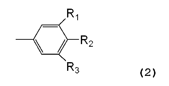
여기서, R1 및 R3은 각각 수소 원자, 할로겐 원자, 치환 혹은 무치환의 알킬기 또는 치환 혹은 무치환의 아릴기이고, 단, R1 및 R3 중 어느 하나는 치환 혹은 무치환의 아릴기이며; R2은 수소 원자, 할로겐 원자 또는 치환 혹은 무치환의 알킬기이다.Wherein each of R 1 and R 3 is a hydrogen atom, a halogen atom, a substituted or unsubstituted alkyl group or a substituted or unsubstituted aryl group, provided that any one of R 1 and R 3 is a substituted or unsubstituted aryl group ; R 2 is a hydrogen atom, a halogen atom or a substituted or unsubstituted alkyl group.
먼저, 일반 화학식 (1)로 표현되는 3차 아릴아민을 설명한다.First, the tertiary arylamine represented by the general formula (1) will be described.
각 Ar1 내지 Ar3으로 표현되는 융합 다환 방향족기의 예는 나프틸 기, 나프틸-d7기, 아세나프틸레닐 기, 안트릴 기, 안트릴-d9 기, 페난트릴 기, 페난트릴-d9 기, 피레닐 기, 피레닐-d9 기, 아세페난트릴레닐 기, 아세안트릴레닐 기, 크리세닐 기, 디벤조크리세닐 기, 벤조안트릴 기, 벤조안트릴-d11 기, 디벤조안트릴 기, 나프트아세닐 기, 피세닐 기, 펜트아세닐 기, 플루오레닐 기, 9,9-디메틸플루오레닐 기, 트리페닐레닐 기, 페릴레닐 기 및 페릴레닐-d11 기를 포함하지만, 이에 제한되지는 않는다.Examples of the fused polycyclic aromatic group represented by each of Ar 1 to Ar 3 include a naphthyl group, a naphthyl-d 7 group, an acenaphthylenyl group, an anthryl group, anthryl-d 9 Phenanthryl group, phenanthryl-d 9 Group, a pyrenyl group, a pyrenyl group -d 9, acetoxy phenanthryl alkylenyl group, ASEAN Trill alkylenyl group, Cri hexenyl group, a dibenzo Cri hexenyl group, an anthryl group, an anthryl group -d 11, dibenzo not benzo benzo Trill group, a naphth-O hexenyl group, blood enyl group, pent-O hexenyl group, a fluorenyl group, a 9,9-dimethyl fluorenyl group, a triphenyl alkylenyl group, a perylenyl group and a carbonyl group perylenyl carbonyl -d 11 But are not limited thereto.
다음으로, 일반 화학식 (1)의 각 Ar1 내지 Ar3로 표현되고, 일반 화학식 (2)로 표현되는 치환 페닐 기에 대해서 설명한다.Next, substituted phenyl groups represented by the general formula (2) represented by Ar 1 to Ar 3 in the general formula (1) will be described.
각 R1 및 R3로 표현되는 할로겐 원자의 예는 불소, 염소, 브롬 및 요오드를 포함한다.Examples of the halogen atom represented by each of R 1 and R 3 include fluorine, chlorine, bromine and iodine.
각 R1 및 R3로 표현되는 치환 또는 무치환의 알킬기의 예는 메틸 기, 메틸-d1기, 메틸-d3 기, 에틸 기, 에틸-d5 기, n-프로필 기, n-부틸 기, n-펜틸 기, n-헥실 기, n-헵틸 기, n-옥틸 기, n-데실 기, 이소-프로필기, 이소-프로필-d7 기, 이소-부틸 기, 세크(sec)-부틸 기, 터트(tert)-부틸 기, 터트-부틸-d9 기, 이소-펜틸 기, 네오펜틸 기, 터트-옥틸 기, 플루오로메틸 기, 디플루오로메틸 기, 트리플루오로메틸 기, 2-플루오로에틸 기, 2,2,2-트리플루오로에틸 기, 퍼플루오로에틸 기, 3-플루오로프로필 기, 퍼플루오로프로필기, 4-플루오로부틸 기, 퍼플루오로부틸 기, 5-플루오로펜틸 기, 6-플루오로헥실 기, 클로로메틸 기, 트리클로로메틸 기, 2-클로로에틸 기, 2,2,2-트리클로로에틸 기, 4-클로로부틸 기, 5-클로로펜틸 기, 6-클로로헥실 기, 브로모메틸 기, 2-브로모에틸 기, 요오도메틸 기, 2-요오도에틸 기, 히드록시메틸 기, 히드록시에틸 기, 시클로프로필기, 시클로부틸 기, 시클로펜틸 기, 시클로헥실 기, 시클로펜틸메틸 기, 시클로헥실메틸 기, 시클로헥실에틸 기, 4-플루오로시클로헥실 기, 노르보닐 기, 아다만틸 기를 포함하지만, 이에 제한되는 것은 아니다.Examples of the substituted or unsubstituted alkyl group represented by each of R 1 and R 3 include a methyl group, a methyl-d 1 group, a methyl-d 3 group, an ethyl group, an ethyl-d 5 group, group, a n- pentyl group, a n- hexyl group, an n- heptyl group, n- octyl group, n- decyl group, an iso-propyl group, iso-propyl -d 7 Group, an iso-butyl group, Gocek (sec) - butyl group, a tert (tert) -butyl group, a tert-butyl -d 9 group, an iso-pentyl group, a neopentyl group, a tert-octyl group, methyl group, fluoro, Trifluoromethyl group, a 2-fluoroethyl group, a 2,2,2-trifluoroethyl group, a perfluoroethyl group, a 3-fluoropropyl group, a perfluoropropyl group, Fluorobutyl group, 6-fluorohexyl group, chloromethyl group, trichloromethyl group, 2-chloroethyl group, 2,2,2-trichloro An ethyl group, a 4-chlorobutyl group, a 5-chloropentyl group, a 6-chlorohexyl group, a bromomethyl group, a 2-bromoethyl group, an iodomethyl group, A cyclohexyl group, a cyclohexyl group, a cyclopentylmethyl group, a cyclohexylmethyl group, a cyclohexylethyl group, a 4-fluorocyclohexyl group, a cyclohexyl group, a cyclohexyl group, Carbonyl group, an acyl it is not just include a butyl, but limited.
각 R1 및 R3로 표현되는 치환 혹은 무치환의 아릴 기의 예로서, 페닐 기, 페닐-d5 기, 4-메틸페닐 기, 4-메톡시페닐 기, 4-에틸페닐 기, 4-플루오로페닐 기, 4-트리플루오로페닐 기, 3,5-디메틸페닐 기, 2,6-디에틸페닐 기, 메시틸 기, 4-터트-부틸페닐 기, 디톨릴아미노페닐 기, 비페닐 기, 터(ter)페닐 기, 나프틸 기, 나프틸-d7 기, 아세나프틸레닐 기, 안트릴 기, 안트릴-d9 기, 페난트릴 기, 페난트릴-d9 기, 피레닐 기, 피레닐-d9 기, 아세페난트릴레닐 기, 아세안트릴레닐 기, 크리세닐 기, 디벤조크리세닐 기, 벤조안트릴 기, 벤조안트릴-d11 기, 디벤조안트릴 기, 나프트아세닐 기, 피세닐 기, 펜타세닐 기, 플루오레닐 기, 트리페닐레닐 기, 페릴레닐 기, 페릴레닐-d11, 및 아래에 표현되는 치환기를 포함하지만, 이에 제한되는 것은 아니다.Examples of the substituted or unsubstituted aryl group represented by each of R 1 and R 3 include a phenyl group, a phenyl-d 5 group, a 4-methylphenyl group, a 4-methoxyphenyl group, A phenyl group, a 4-trifluorophenyl group, a 3,5-dimethylphenyl group, a 2,6-diethylphenyl group, a mesityl group, a 4-tert- , A terphenyl group, a naphthyl group, a naphthyl-d 7 group, an acenaphthylenyl group, an anthryl group, anthryl-d 9 A phenanthryl group, a phenanthryl-d 9 group, a pyrenyl group, pyrenyl-d 9 Group, acetoxy phenanthryl alkylenyl group, ASEAN Trill alkylenyl group, Cri hexenyl group, a dibenzo Cri hexenyl group, a benzo-anthryl group, a benzo anthryl -d 11 group, a dibenzo-anthryl group, a naphth-O hexenyl group, a hexenyl blood But are not limited to, a phenyl group, a pentacenyl group, a fluorenyl group, a triphenylenyl group, a perylenyl group, perylenyl-d 11 , and substituents represented below.
<화학식>≪

정공 수송층에 포함되는 가장 작은 이온화 포텐셜의 유기 화합물은 전자가 분자 전체에 분포되지 않은 분자구조를 갖는 것이 바람직하다. 이온화 포텐셜이 가장 작은 유기 화합물이 전자가 분자 전체에 분포되지 않은 분자구조를 갖는 경우, 유기 화합물은 라디칼 양이온 상태에서 청색 발광 파장 영역에 흡수 피크를 갖지 않는다. 따라서 이온화 포텐셜이 가장 작은 유기 화합물은 청색 발광으로 여기되지 않고, 청색 발광에 의해 구조 변화를 억제할 수 있다.The organic compound having the smallest ionization potential included in the hole transport layer preferably has a molecular structure in which electrons are not distributed throughout the molecule. When the organic compound having the smallest ionization potential has a molecular structure in which electrons are not distributed throughout the molecule, the organic compound has no absorption peak in the blue light emission wavelength region in the radical cation state. Therefore, the organic compound having the smallest ionization potential is not excited by the blue light emission, and the blue light emission can suppress the structural change.
전자가 분자 전체에 분포되는 것을 방지할 수 있는 화합물의 구체적인 예는 정공 수송 능력이 탁월한 3차 아릴아민 유도체를 포함한다. 특히, 전자가 분자 전체에 분포되지 않는 비틀어진 구조를 가질 것으로 기대되기 때문에 일반 화학식 (1)의 화합물이 바람직하다.Specific examples of the compound capable of preventing electrons from being distributed throughout the molecule include tertiary arylamine derivatives having excellent hole transporting ability. Particularly, the compound of the general formula (1) is preferred because it is expected that electrons will have a twisted structure that is not distributed throughout the molecule.
일반 화학식 (1)의 3차 아릴아민 유도체는 Ar1 내지 Ar3의 앞서 언급한 내용으로부터 이해되는 바와 같이 상대적으로 분자량이 큰 화합물이고, 그 분자량은 진공증착법에 의한 박막 형성이 가능하게 하기 위하여 1500 이하가 바람직하다.The tertiary arylamine derivative represented by general formula (1) is a compound having a relatively high molecular weight as understood from the above-mentioned contents of Ar 1 to Ar 3 , and its molecular weight is 1500 Or less.
또 일반 화학식 (2)에서, R1 및 R3(메타 위치)의 어느 하나로 치환 혹은 무치환 아릴 기를 도입하는 것은, 그러한 기의 도입이 분자의 결정성을 감소할 수 있기 때문에 바람직하다. 한편, 일반 화학식 (2)에서, R2에 알킬기 또는 할로겐 원자를 도입하는 것이 R2가 수소 원자를 나타내는 경우에 비해 HOMO를 보다 크게 변화시킬 수 있기 때문에 바람직하다. 구체적으로, 알킬기의 도입은 HOMO를 얕게 할 수 있는 반면, 할로겐 원자를 도입하면 HOMO를 깊게 할 수 있다. 일반 화학식 (2)에 있어서, 아릴기를 R2에 도입하지 않는 것을 권장한다. 이는 R2의 위치에 아릴 기의 도입에 의해 전자가 더 넓게 분포할 수 있기 때문이다.In the general formula (2), the introduction of the substituted or unsubstituted aryl group into any one of R 1 and R 3 (meta position) is preferable since such a group can reduce the crystallinity of the molecule. On the other hand, it is preferable because in the general formula (2), that is R 2 for introducing an alkyl group or a halogen atom in R 2 can be more largely changed than the HOMO to indicate a hydrogen atom. Specifically, introduction of an alkyl group can make the HOMO shallow, while introducing a halogen atom can deepen the HOMO. In general formula (2), it is recommended not to introduce an aryl group into R 2 . This is because electrons can be distributed more widely by the introduction of an aryl group at the position of R < 2 & gt ;.
일반 화학식 (1)로 표현되는 화합물의 구체적인 예를 아래에서 열거한다. 본 발명은 그 예에 제한되는 것이 아니라는 것을 알아야 한다.Specific examples of the compound represented by the general formula (1) are listed below. It should be understood that the invention is not limited to that example.
<화학식>≪


정공 수송층에 포함되는 유기 화합물 중에서 앞서 언급한 "다른 유기 화합물"에 해당하는 화합물의 구체적인 구조는 특별히 제한되지 않는다. 그 중에서 트리페닐아민 유도체가 바람직하다.The specific structure of the above-mentioned "other organic compound" among the organic compounds contained in the hole transporting layer is not particularly limited. Among them, triphenylamine derivatives are preferable.
본 발명의 발명자는 정공 수송층의 구성 재료가 정공과 결합하여 라디칼 양이온 상태로 되는 경우, 광과 같은 에너지를 수취하는 것으로 여기 상태로 되는 사실에 주목하였다.The inventors of the present invention paid attention to the fact that when the constituent material of the hole transporting layer is in a state of a radical cation by binding with holes, it is excited by receiving energy such as light.
여기 상태로 되면, 정공 수송층의 구성 재료는 비가역적인 반응을 겪어 구조변화를 야기하는 것으로 생각된다. 비록 구조 변화의 구체적인 측면은 분명하지 않지만, 분자 구조의 변화는 예를 들면, 절단 반응, 분해 반응, 부가 반응 등에 의해 발생되는 것으로 생각된다. 분자구조의 변화는 캐리어 수송성 및 전도 레벨 (HOMO/LUMO 등에 의해 나타내어지는 캐리어 수송 시의 에너지 준위)의 변화를 이끈다. 그러면, 발광층의 캐리어 밸런스가 무너지고, 발광층에서 정공과 전자의 재결합 확률의 저하를 야기한다. 또한 여기 상태의 상기 언급한 분자 (구성 재료)가 발광 분자의 소광체(quencher)로 기능하여, 또한 발광 강도의 저하를 야기한다.In the excited state, the constituent material of the hole transport layer is believed to undergo an irreversible reaction to cause a structural change. Although a specific aspect of the structural change is not clear, it is considered that the change of the molecular structure is caused by, for example, a cleavage reaction, a decomposition reaction, an addition reaction, or the like. Changes in the molecular structure lead to changes in carrier transport and conduction levels (energy levels at the time of carrier transport represented by HOMO / LUMO, etc.). Then, the carrier balance of the light emitting layer is collapsed, and the probability of recombination of holes and electrons in the light emitting layer is lowered. In addition, the above-mentioned molecule (constituent material) in the excited state functions as a quencher of the luminescent molecule, and also causes a decrease in luminescence intensity.
유기 발광 소자를 구동할 때, 애노드로부터 공급되는 정공은 정공 수송층을 통해 발광층에 공급된다. 한편, 캐소드로부터 공급되는 전자는 전자 수송층을 통해 발광층에 공급된다. 여기서 정공 수송층의 구성 재료가 되는 화합물은, 반복적으로 정공과 결합되고 해리된다. 이것은 전기 화학적으로 산화 및 환원을 반복되어, 라디칼 양이온 상태 및 중성 상태를 반복하는 결과를 낳는다는 것을 의미한다. 즉, 소자에 전류를 인가할 때, 라디칼 양이온 상태의 다수의 유기 화합물이 정공 수송층에 존재한다. 라디칼 양이온 상태에 있는 유기 화합물이 또한 광과 같은 에너지를 받아 여기 상태가 되면, 화합물 자체의 구조가 변화하는 것으로 생각된다. 이것이 유기 발광 소자의 연속 구동 시의 내구성을 감소시킨다.When driving the organic light emitting element, the holes supplied from the anode are supplied to the light emitting layer through the hole transporting layer. On the other hand, electrons supplied from the cathode are supplied to the light emitting layer through the electron transporting layer. Here, the compound which becomes the constituent material of the hole transporting layer is repeatedly bonded and disassociated with holes. This means that the oxidation and reduction are repeated electrochemically, resulting in repeating the radical cation state and the neutral state. That is, when a current is applied to the device, a large number of organic compounds in a radical cation state exist in the hole transporting layer. It is believed that when the organic compound in the radical cation state is also in the excited state by receiving energy such as light, the structure of the compound itself is changed. This reduces the durability in continuous driving of the organic light emitting element.
라디칼 양이온 상태의 유기 화합물에 의해 받아들여지는 것으로 고려되는 에너지는 예를 들어, 다음의 두가지 에너지로 생각된다.The energy considered to be accepted by the organic compound in the radical cation state is considered, for example, as two energies:
그 중 하나는 발광 재료와 같은 발광층의 구성 재료의 여기 에너지다. 정공 수송층이 대부분의 경우에 발광층에 인접하기 때문에, 발광층이 발광하고 있을 때, 발광층의 구성 재료의 여기 에너지의 일부가 정공 수송층으로 에너지 이동을 겪을 수 있다. 구체적으로 이것은 단일항 여기 상태로부터 포엘스터(Foerster) 형태의 에너지 이동이다.One of them is the excitation energy of the constituent material of the light emitting layer such as the light emitting material. Since the hole transporting layer is adjacent to the light emitting layer in most cases, when the light emitting layer is emitting light, a part of the excitation energy of the constituent material of the light emitting layer may undergo energy transfer to the hole transporting layer. Specifically, it is a Foerster-type energy transfer from a single anti-excited state.
그 중 나머지는 청색 발광의 광 에너지가 발광층으로부터 발광하는 것이다. 라디칼 양이온 상태의 화합물은 광을 흡수함으로써 여기될 수 있다.And the remainder is the light energy of blue light emission from the light emitting layer. A compound in a radical cation state can be excited by absorbing light.
두 에너지 모두 유기 발광 소자의 발광으로부터 유도되고, 라디칼 양이온 상태의 유기 화합물에 영향을 주는 에너지이다. 특히, 그 에너지 전달의 효율 면에서, 첫번째 것이 지배적인 것으로 생각된다.Both energies are derived from the emission of organic light emitting devices and affect the organic compounds in the radical cation state. Particularly, in terms of efficiency of energy transfer, the first one seems to be dominant.
라디칼 양이온 상태의 유기 화합물이 상대적으로 안정적이지만, 라디칼 양이온 상태에 있는 유기 화합물이 더 에너지를 받아서 여기 상태로 되는 경우, 유기 화합물이 불안정하게 되어 구조의 변화를 겪는 것으로 생각된다.It is considered that when the organic compound in the radical cation state is relatively stable but the organic compound in the radical cation state becomes the excited state by receiving more energy, the organic compound becomes unstable and undergoes a change in the structure.
앞서 언급한 바와 같이, 전류 전도 동안에 정공 수송층에 포함되는 유기 화합물의 구조 변화를 방지하기 위해서는, 정공을 수취하기 쉬운 유기 화합물이 라디칼 양이온 상태에서 청색 파장 영역에 흡수 피크를 갖지 않는 화합물인 것이 필요하다. 또한 정공 수송층에 라디칼 양이온 상태의 분자를 없애는 방법도 고려된다. 그러나 정공을 수송하는 정공 수송층의 기능을 고려하면, 그 방법은 이용할 수 없다.As described above, in order to prevent the structural change of the organic compound contained in the hole transporting layer during the current conduction, it is necessary that the organic compound which is easy to take holes is a compound which does not have an absorption peak in the blue wavelength region in the radical cation state . Further, a method of eliminating molecules having a radical cation state in the hole transport layer is also considered. However, considering the function of the hole transporting layer for transporting holes, the method can not be used.
전술한 점에서, 본 발명에서, 정공 수송층에 포함되는 복수 종류의 유기 화합물, 특히, 정공을 받기 쉬운 유기 화합물은 정공을 받아 라디칼 양이온 상태로 되었을 때 청색 파장 영역에서 흡수 피크를 갖지 않는 유기 화합물이 선택된다.In view of the above, in the present invention, in the present invention, a plurality of kinds of organic compounds contained in the hole transporting layer, particularly, organic compounds that are susceptible to holes are organic compounds that do not have absorption peaks in the blue wavelength region Is selected.
결론적으로, 정공을 받기 쉬운 유기 화합물은 발광층으로부터 청색 발광 출력 때문에 구조 변화를 겪지 않는다. 또한 불필요한 정공의 축적에 의해 야기되는 정공을 받기 쉬운 유기 화합물의 구조 변화도 방지할 수 있다.Consequently, organic compounds that are susceptible to holes do not suffer structural changes due to the blue light emission output from the light emitting layer. It is also possible to prevent a change in the structure of the organic compound, which is susceptible to holes, caused by the accumulation of unnecessary holes.
앞서 설명한 바와 같이, 라디칼 양이온 상태의 유기 화합물이 발광층으로부터 방출되는 광에 의해 여기되면, 유기 화합물의 발광 강도는 실제로 저하된다.As described above, when the organic compound in the radical cation state is excited by the light emitted from the light emitting layer, the light emission intensity of the organic compound is actually lowered.
예를 들면, 기판 상에 아래의 표로 나타내지는 구성을 갖는 유기 발광 소자가 있다고 가정한다 (구성은 기판상에 적층되는 순서에 따라서 기재되어 있음에 주의한다).For example, it is assumed that there is an organic light emitting element having a configuration shown in the following table on the substrate (note that the configuration is described in the order of stacking on the substrate).
화합물 2 (10 중량%)Compound 1 (90% by weight)
Compound 2 (10% by weight)
상기 언급한 화합물 1 내지 3은 하기에 나타내지는 화합물이다. 또한, 상기 언급된 표의 유기 발광 소자는 수분의 흡착이 일어나지 않도록, -70 ℃ 이하의 노점에서, 질소분위기에서 보호용 유리판을 덮고, 에폭시계 접착재로 밀봉한다. The above-mentioned
<화학식>≪
유기 발광 소자에 전압을 인가하면, 화합물 3의 전자친화력이 작기 때문에, 전자가 캐소드로부터 제2 유기 화합물 층에 주입되지 않지만, 정공이 애노드로부터 제2 유기 화합물 층에 주입된다. 따라서 정공 전류만이 유기 발광 소자를 통해 흐른다. 이에 따라, 이 샘플을 통해 전류가 흘러도 EL 발광은 일어나지 않는다.When a voltage is applied to the organic light emitting element, since the electron affinity of the compound 3 is small, electrons are not injected from the cathode into the second organic compound layer, but holes are injected from the anode into the second organic compound layer. Therefore, only the hole current flows through the organic light emitting element. Thus, EL light emission does not occur even if a current flows through this sample.
유기 발광 소자에서, 다음의 조건 하에서 제1 유기 화합물 층의 광발광(photoluminescence)을 측정한다. 다음의 조건 (i) 내지 (iii)은 각각 130 시간 행해진다.In the organic light emitting device, the photoluminescence of the first organic compound layer is measured under the following conditions. The following conditions (i) to (iii) are carried out for 130 hours each.
(i) 전압을 전류밀도를 100 mA/cm2으로 유지하는 동안에 인가한다.(i) The voltage is applied while the current density is maintained at 100 mA / cm < 2 >.
(ii) 파장 460 nm인 광을 조사한다.(ii) Light having a wavelength of 460 nm is irradiated.
(iii) 전류밀도를 100 mA/cm2으로 유지하는 동안에 전압을 인가하면서 파장 460 nm의 광을 조사한다.(iii) While the current density is maintained at 100 mA / cm < 2 >, a voltage of 460 nm is irradiated while applying a voltage.
광발광의 측정 결과를 다음의 표에 나타낸다. 또한 조건 (i) 및 (iii)에 대해서는 전압 변화의 결과도 또한 나타낸다.The measurement results of the photoluminescence are shown in the following table. Also for the conditions (i) and (iii), the result of the voltage change is also shown.
(주 1) 전류 전도 및/또는 광 조사 전에 대하여 전류 전도 및/또는 광 조사 후에 광발광 강도. 전류 전도 및 광 조사 각각의 시간은 130 시간이다.(Note 1) Photoluminescence intensity after current conduction and / or light irradiation prior to current conduction and / or light irradiation. Each time of current conduction and light irradiation is 130 hours.
(주 2) 전류 전도 및/또는 광 조사의 시작 시의 전압은 약 21 V이다.(Note 2) The voltage at the start of current conduction and / or light irradiation is about 21 V.
한편, 상기 표 2의 결과를 고찰하는 목적에서, 화합물 2의 박막의 UV-가시 흡수 스펙트럼도 측정한다. 도 1은 중성상태 및 라디칼 양이온 상태에서 UV-가시 흡수 스펙트럼을 나타낸다. 여기서 사용되는 중성상태는 화합물 2의 박막이 양이온과 결합하지 않고 있는 상태, 즉 유기 발광 소자에서 전압을 인가하지 않고 있는 상태를 나타낸다. 한편, 여기서 사용되는 라디칼 양이온 상태는 화합물 2의 박막이 양이온과 결합하고 있는 상태, 즉 유기 발광 소자에 전압을 인가하고 있는 상태를 나타낸다.On the other hand, for the purpose of examining the results of Table 2, the UV-visible absorption spectrum of the thin film of
도 1을 참조하면, 표 2에 나타내지는 결과는 정공을 통한 전류 전도에 의해 발생되는 화합물 2의 라디칼 양이온이 460 nm 파장의 청색광으로 여기되어, 구조의 변화를 야기한다고 생각된다. 화합물 2는 중성상태(도 1의 스펙트럼 1)에서는 청색 파장 영역에서 흡수가 상대적으로 적고, 에너지 간격이 넓기 때문에, 약 460 nm의 파장을 갖는 청색광으로 여기될 수 없다. 그러나 라디칼 양이온 상태(도 1의 스펙트럼 2)가 되면, 화합물이 청색 파장 영역에서 흡수 피크를 갖기 때문에, 라디칼 양이온 상태의 화합물 2는 약 460 nm의 파장을 갖는 청색광으로 여기된다. 화합물 2는 화합물 1보다 이온화 포텐셜이 더 작기 때문에, 우선적으로 라디칼 양이온 상태로 된다.Referring to FIG. 1, the results shown in Table 2 indicate that the radical cation of
상기 언급한 결과는 정공을 통한 전류 전도에 의해 발생된 라디칼 양이온의 흡수 스펙트럼이 소자의 특성을 변화시킬 수 있다는 것을 시사한다.The above-mentioned results suggest that the absorption spectrum of the radical cation generated by current conduction through holes can change the characteristics of the device.
유기 발광 소자에서 앞서 언급한 소자 특성의 변화에 관하여, 발광층으로부터 유출하는 가능성이 있는 발광에 필요한 여기 에너지를 고려하여야 한다. 왜냐하면, 포엘스터 이동형의 에너지 전달의 효율이 광 흡수보다 현저하게 크기 때문이다.With respect to the above-mentioned change in the device characteristics in the organic light emitting device, it is necessary to consider the excitation energy required for light emission that may flow out from the light emitting layer. This is because the efficiency of the energy transfer of the Forster transport type is significantly greater than that of light absorption.
본 발명에서, 발광층은 청색 발광하는 유기 화합물만으로 형성되어도 되고, 호스트 및 게스트로 형성되어도 된다. 발광층이 호스트 및 게스트로 형성되어 있는 경우, 호스트 및 게스트는 중량비 (중량%)와 같은 발광층 내의 함량에 의해 서로 구별될 수 있다. 이 경우 게스트는 발광층으로부터 출력되는 발광의 색을 결정하는 재료이다. 발광층이 호스트 및 게스트로 형성되는 경우, 호스트 및 게스트 이외에, 예를 들면 호스트로부터 게스트로의 에너지 이동을 더욱 용이하게 하는 소위 어시스트 도펀트와 같은 재료를 또한 첨가할 수도 있다.In the present invention, the light-emitting layer may be formed of only an organic compound that emits blue light, or may be formed of a host and a guest. In the case where the light emitting layer is formed as a host and a guest, the host and the guest can be distinguished from each other by the content in the light emitting layer such as the weight ratio (wt%). In this case, the guest is a material for determining the color of light emitted from the light emitting layer. When the light emitting layer is formed as a host and a guest, a material such as a so-called assist dopant which further facilitates energy transfer from, for example, a host to a guest in addition to the host and the guest may also be added.
본 발명에서, 정공 수송층 및 발광층의 이외에 또다른 층이 유기 화합물층을 형성하는 층으로 제공되는 경우에는, 공지의 재료를 또다른 층의 구성 재료 (정공 주입/수송 재료, 전자 주입/수송 재료 및 발광 재료)로서 사용할 수 있다. 또한 본 발명에서, 전극 (애노드 및 캐소드)의 구성 재료로서 공지의 재료 (금속재료, 합금, 금속화합물 등)을 사용할 수 있다.In the present invention, when another layer other than the hole transporting layer and the light emitting layer is provided as a layer for forming an organic compound layer, a known material may be used as the constituent material (hole injecting / transporting material, electron injecting / transporting material, Material). In the present invention, well-known materials (metal materials, alloys, metal compounds, etc.) can be used as constituent materials of the electrodes (anode and cathode).
본 발명의 유기 발광 소자는, 예를 들면, 표시 장치의 화소부, 전자사진 화상 형성 장치의 감광체의 잠상을 형성시키기 위한 광원, 또는 화상 광학계를 갖는 화상 장치의 표시부로 이용될 수 있다.The organic light emitting element of the present invention can be used, for example, as a display portion of an image device having a pixel portion of a display device, a light source for forming a latent image of a photosensitive member of an electrophotographic image forming apparatus, or an image optical system.
표시 장치 부재로서 본 발명의 유기 발광 소자를 이용하는 경우, 이 표시 장치는 본 발명의 유기 발광 소자 및 본 발명의 유기 발광 소자의 휘도를 제어하는 TFT 회로를 갖는 화소를 포함한다.When the organic light emitting element of the present invention is used as the display device member, the display device includes the organic light emitting element of the present invention and the pixel having the TFT circuit for controlling the luminance of the organic light emitting element of the present invention.
(실시예)(Example)
(합성예 1) 예시 화합물 1의 합성(Synthesis Example 1) Synthesis of
다음의 합성 기법에 의해 예시 화합물 1을 합성하였다.
<반응식> <Reaction Scheme>
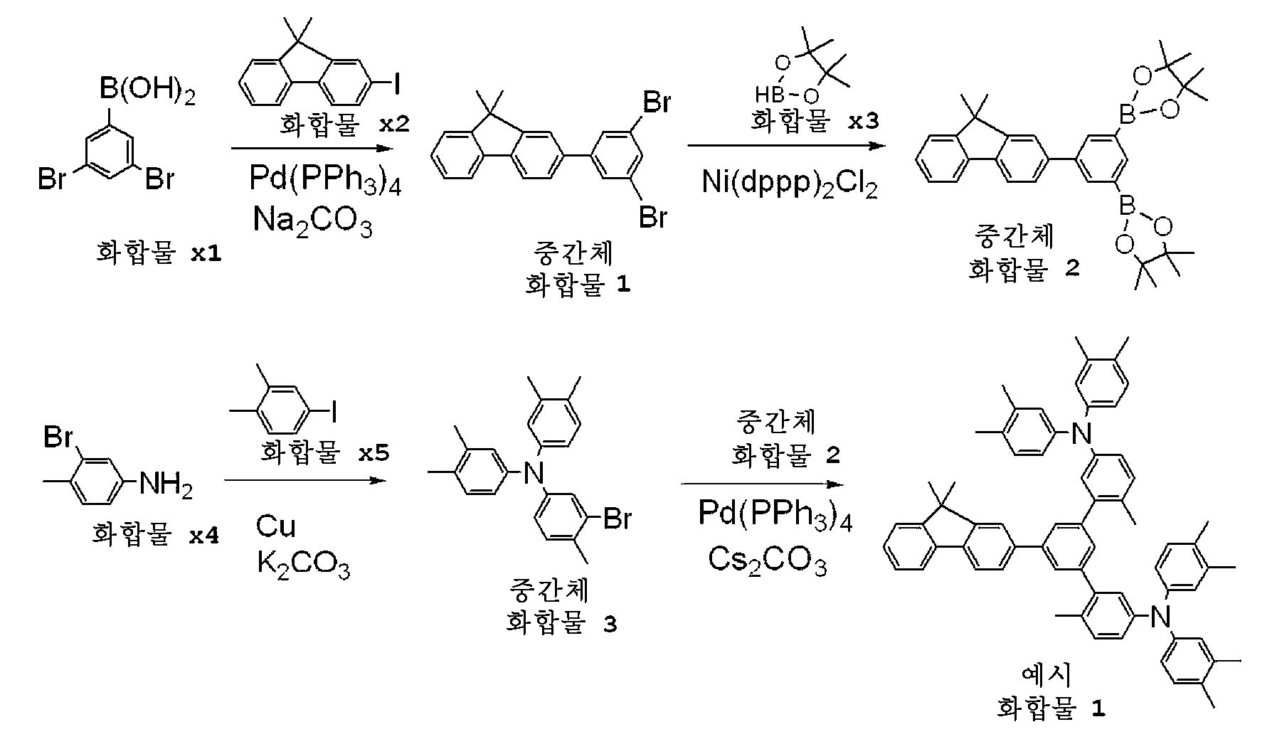
(1) 중간화합물 1의 합성(1) Synthesis of
다음의 시약 및 용매를 300 ml의 3구 플라스크에 채웠다.The following reagents and solvents were charged into a 300 ml three-necked flask.
화합물 x1: 10 g (36.2 mmol)Compound x1: 10 g (36.2 mmol)
화합물 x2: 14.98 g (47.1 mmol)Compound x2: 14.98 g (47.1 mmol)
톨루엔: 120 mlToluene: 120 ml
에탄올: 20 mlEthanol: 20 ml
다음으로, 반응계 내를 질소분위기로 바꾼 후, 반응 용액을 실온에서 휘저으면서, 탄산나트륨 10 g과 물 100 ml을 혼합한 수용액을 떨어뜨리고, 그 후 테트라키스(트리페닐포스핀)팔라듐(0) 2.00g (1.70 mmol)을 용액에 첨가하였다. 그 후, 반응 용액을 77℃로 가열하고, 이 온도(77℃)에서 5시간 휘저었다. 반응 완료 후, 유기층을 톨루엔으로 추출하고, 무수황산나트륨에서 건조시킨 후, 용매를 감압하에서 증류하여 조(crude) 생성물을 얻었다. 다음으로, 이 조 생성물을 실리카겔 칼럼 크로마토그래피(전개 용매:헵탄/톨루엔 혼합 용매)로 정제하여, 백색 고체로서 중간화합물 1, 9.84 g (수율: 64.1 %)을 얻었다.Next, an aqueous solution obtained by mixing 10 g of sodium carbonate and 100 ml of water was dropped while the inside of the reaction system was changed to a nitrogen atmosphere, and then tetrakis (triphenylphosphine) palladium (0) 2.00 g (1.70 mmol) was added to the solution. Thereafter, the reaction solution was heated to 77 DEG C and stirred at this temperature (77 DEG C) for 5 hours. After completion of the reaction, the organic layer was extracted with toluene, dried over anhydrous sodium sulfate, and then the solvent was distilled off under reduced pressure to obtain a crude product. Subsequently, this crude product was purified by silica gel column chromatography (developing solvent: heptane / toluene mixed solvent) to obtain 9.84 g (yield: 64.1%) of
(2) 중간화합물 2의 합성(2) Synthesis of
다음의 시약 및 용매를 300 ml의 3구 플라스크에 채웠다.The following reagents and solvents were charged into a 300 ml three-necked flask.
중간화합물 1: 8.0 g (18.9 mmol)Intermediate Compound 1: 8.0 g (18.9 mmol)
톨루엔: 120 mlToluene: 120 ml
트리에틸아민: 40 mlTriethylamine: 40 ml
다음으로, 화합물 x3 (11.0 ml)을 한 방울씩 첨가하였다. 다음으로, 반응계 내를 질소분위기로 바꾼 후, 실온에서 휘저으면서, [1,3-비스(디페닐포스피노)프로판]니켈(II) 디클로라이드 1.08 g (2.0 mmol)을 반응 용액에 첨가하였다. 그 후, 반응 용액을 90℃로 가열하고, 이 온도(90℃)에서 8시간 휘저었다. 반응 완료 후, 유기층을 톨루엔으로 추출하고, 무수황산나트륨에서 건조시킨 후, 용매를 감압하에서 증류하여 조 생성물을 얻었다. 다음으로, 조 생성물을 실리카겔 칼럼 크로마토그래피 (전개 용매: 헵탄/톨루엔 혼합 용매)로 정제하여, 황백색 고체로서 중간화합물 2, 5.25 g (수율: 53.4%)을 얻었다.Next, compound x3 (11.0 ml) was added dropwise. Next, 1.08 g (2.0 mmol) of [1,3-bis (diphenylphosphino) propane] nickel (II) dichloride was added to the reaction solution while changing the inside of the reaction system to nitrogen atmosphere and then stirring at room temperature. Thereafter, the reaction solution was heated to 90 占 폚 and stirred at this temperature (90 占 폚) for 8 hours. After completion of the reaction, the organic layer was extracted with toluene, dried over anhydrous sodium sulfate, and then the solvent was distilled off under reduced pressure to obtain a crude product. Subsequently, the crude product was purified by silica gel column chromatography (developing solvent: heptane / toluene mixed solvent) to obtain 5.25 g (yield: 53.4%) of
(3) 중간화합물 3의 합성(3) Synthesis of Intermediate Compound 3
다음의 시약 및 용매를 200 ml 삼구 플라스크에 채웠다.The following reagents and solvents were charged into a 200 ml three-necked flask.
화합물 x4: 5.0 g (26.9 mmol)Compound x4: 5.0 g (26.9 mmol)
화합물 x5: 25 g (108 mmol)Compound x5: 25 g (108 mmol)
구리분: 7.0 g (110 mmol)Copper powder: 7.0 g (110 mmol)
탄산 칼륨: 20.73 g (150 mmol)Potassium carbonate: 20.73 g (150 mmol)
o-디클로로벤젠: 100 mlo-Dichlorobenzene: 100 ml
다음으로, 반응 용액을 165℃로 가열하고, 이 온도(165℃)에서 8시간 휘저었다. 반응 완료 후, 반응 용액을 여과하고, 그 여액을 감압하에서 농축하여 조 생성물을 얻었다. 그 후, 조 생성물을 실리카겔 칼럼 크로마토그래피 (전개 용매:헵탄/톨루엔 혼합 용매)로 정제하여, 백색 고체로서 중간화합물 3, 9.07 g (수율: 86.0%)을 얻었다.Next, the reaction solution was heated to 165 DEG C and stirred at this temperature (165 DEG C) for 8 hours. After completion of the reaction, the reaction solution was filtered, and the filtrate was concentrated under reduced pressure to obtain a crude product. Subsequently, the crude product was purified by silica gel column chromatography (developing solvent: heptane / toluene mixed solvent) to obtain 9.07 g (yield: 86.0%) of intermediate compound 3 as a white solid.
(4) 예시 화합물 1의 합성(4) Synthesis of
다음의 시약 및 용매를 200 ml 삼구 플라스크에 채웠다.The following reagents and solvents were charged into a 200 ml three-necked flask.
중간화합물 2: 0.78 g (1.5 mmol)Intermediate compound 2: 0.78 g (1.5 mmol)
중간화합물 3: 1.47 g (3.75 mmol)Intermediate compound 3: 1.47 g (3.75 mmol)
톨루엔: 50 mlToluene: 50 ml
에탄올: 10 mlEthanol: 10 ml
다음으로, 반응계 내를 질소분위기로 바꾼 후, 반응 용액을 실온에서 휘저으면서, 탄산 세슘 10 g 및 물 50 ml를 혼합한 수용액을 떨어뜨리고, 다음에 테트라키스(트리페닐포스핀)팔라듐(0) 0.2 g (0.170 mmol)을 첨가하였다. 그 후, 반응 용액을 77℃로 가열하고, 이 온도(77℃)에서 5시간 휘저었다. 반응 종료 후, 유기층을 톨루엔으로 추출하고, 무수 황산 나트륨에서 건조시킨 후, 용매를 감압하에서 증류하여 조 생성물을 얻었다. 그 다음, 조 생성물을 실리카겔 칼럼 크로마토그래피(전개 용매:헵탄/톨루엔 혼합 용매)로 정제하여, 황백색 고체로서 예시 화합물 1, 0.82 g (수율: 60.8%)을 얻었다.Next, an aqueous solution obtained by mixing 10 g of cesium carbonate and 50 ml of water was dropped while stirring the reaction solution at room temperature, and then tetrakis (triphenylphosphine) palladium (0) was added thereto, 0.2 g (0.170 mmol) was added. Thereafter, the reaction solution was heated to 77 DEG C and stirred at this temperature (77 DEG C) for 5 hours. After completion of the reaction, the organic layer was extracted with toluene, dried over anhydrous sodium sulfate, and then the solvent was distilled off under reduced pressure to obtain a crude product. Subsequently, the crude product was purified by silica gel column chromatography (developing solvent: heptane / toluene mixed solvent) to obtain 0.82 g (yield: 60.8%) of
매트릭스 보조 레이저 탈착/이온화 비행시간형 질량분석기(MALDI-TOF MS)에 따라서, 예시 화합물 1의 M+인 896을 확인하였다.According to a matrix assisted laser desorption / ionization time-of-flight mass spectrometer (MALDI-TOF MS), 896 of M + of
또한, 1H-NMR 측정에 의해, 예시 화합물 1의 구조를 확인하였다.Further, the structure of
1H-NMR (CDCl3, 400 MHz)σ(ppm): 7.76-7.73 (m, 2H), 7.63 (s, 1H), 7.57 (d, 1H), 7.48-7.44 (m, 3H), 7.36-7.30 (m, 2H), 7.20 (s, 1H), 7.12 (d, 2H), 7.03-6.92 (m, 12H), 6.84 (dd, 4H), 2.27 (s, 6H), 2.20 (s, 12H), 2.16 (s, 12H), 1.52 (s, 6H) 1 H-NMR (CDCl 3, 400 MHz) σ (ppm): 7.76-7.73 (m, 2H), 7.63 (s, 1H), 7.57 (d, 1H), 7.48-7.44 (m, 3H), 7.36- 2H), 7.20 (s, 1H), 7.12 (d, 2H), 7.03-6.92 (m, 12H), 6.84 (dd, , 2.16 (s, 12 H), 1.52 (s, 6 H)
(합성예 2) 예시 화합물 2의 합성(Synthesis Example 2) Synthesis of
다음의 합성 기법에 의해 예시 화합물 2를 합성하였다.
<반응식> <Reaction Scheme>
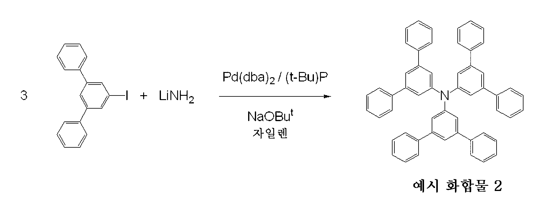
다음의 시약 및 용매를 300 ml 삼구 플라스크에 채웠다.The following reagents and solvents were charged into a 300 ml three-necked flask.
3'-요오도-1,1':5',1"-터페닐: 4 g (순도:93 %, 10.5 mmol)4'-iodo-1,1 ': 5', 1 "-terphenyl: 4 g (purity: 93%, 10.5 mmol)
리튬 아미드 (상품명, 키시다 케미칼 코., 엘티디.에서 제조됨): 2.68 g (111 mmol)Lithium amide (trade name, manufactured by Kishida Chemical Co., Ltd.): 2.68 g (111 mmol)
나트륨 터트-부톡시드 (상품명, 도쿄 케미칼 인더스트리 코., 엘티디.에서 제조됨): 3.41 g (34.8 mmol)Sodium tert-butoxide (trade name, manufactured by Tokyo Chemical Industry Co, Ltd.): 3.41 g (34.8 mmol)
자일렌: 150 mlXylene: 150 ml
다음으로, 반응계 내를 질소분위기로 바꾼 후, 반응 용액을 실온에서 휘저으면서, 트리-터트-부틸포스핀 (10 중량% 헥산 용액) 3.7 ml (0.15 mmol)을 첨가하였다. 그 후, 팔라듐 디벤질리덴아세톤 (상품명, 도쿄 케미칼 인더스트리 코., 엘티디.에서 제조됨) 0.37 mg (0.65 mmol)을 첨가하였다. 그 후, 플라스크 내에 아르곤을 도입하여 반응계를 아르곤으로 바꾼다. 그 후에 반응 용액을 가열 및 환류시키면서 6시간 휘저었다. 반응 완료 후, 반응 용액 중의 유기층을 톨루엔으로 수집하였다. 그 후, 이 유기층을 물로 세척하고, 무수 황산 나트륨에서 건조시키고, 용매를 감압하에서 증류하여 조 생성물을 얻었다. 다음으로, 조 생성물을 실리카겔 칼럼 크로마토그래피 (전개 용매: 헵탄/톨루엔 혼합 용매)에서 3회 정제하여, 백색 결정으로서 예시 화합물 2, 0.4 g (수율: 16 %)을 얻었다.Subsequently, 3.7 ml (0.15 mmol) of tri-tert-butylphosphine (10 wt% hexane solution) was added while the reaction system was changed to nitrogen atmosphere and the reaction solution was stirred at room temperature. Then 0.37 mg (0.65 mmol) of palladium dibenzylidene acetone (trade name, manufactured by Tokyo Chemical Industry Co, Ltd.) was added. Thereafter, argon was introduced into the flask, and the reaction system was changed to argon. Thereafter, the reaction solution was stirred for 6 hours while heating and refluxing. After completion of the reaction, the organic layer in the reaction solution was collected with toluene. Thereafter, the organic layer was washed with water, dried over anhydrous sodium sulfate, and the solvent was distilled off under reduced pressure to obtain a crude product. Subsequently, the crude product was purified three times on silica gel column chromatography (developing solvent: heptane / toluene mixed solvent) to obtain 0.4 g (yield: 16%) of
매트릭스 보조 레이저 탈착/이온화 비행시간형 질량분석기(MALDI-TOF MS)에 따라서, 예시 화합물 2의 M+인 701을 확인하였다.According to a matrix assisted laser desorption / ionization time-of-flight mass spectrometer (MALDI-TOF MS), M + 701 of
또한, 1H-NMR 측정에 의해, 예시 화합물 2의 구조를 확인하였다.Further, the structure of
1H-NMR (CDCl3, 400 MHz (제올 엘티디.에 의해 제조된 ECA-400으로 측정))σ (ppm): 7.60-7.58 (4H, m), 7.52 (1.1H, t), 7.48 (2H, d), 7.40 (4H, dt), 7.32 (2H, tt) 1 H-NMR (CDCl 3, 400 MHz ( measured by the ECA-400 manufactured by JEOL El tidi).) Σ (ppm): 7.60-7.58 (4H, m), 7.52 (1.1H, t), 7.48 ( 2H, d), 7.40 (4H, dt), 7.32 (2H, tt)
(합성예 3) 예시 화합물 3의 합성(Synthesis Example 3) Synthesis of Exemplified Compound 3
다음의 합성 기법에 의해 예시 화합물 3을 합성했다.Exemplified Compound 3 was synthesized by the following synthesis technique.
<반응식><Reaction Scheme>
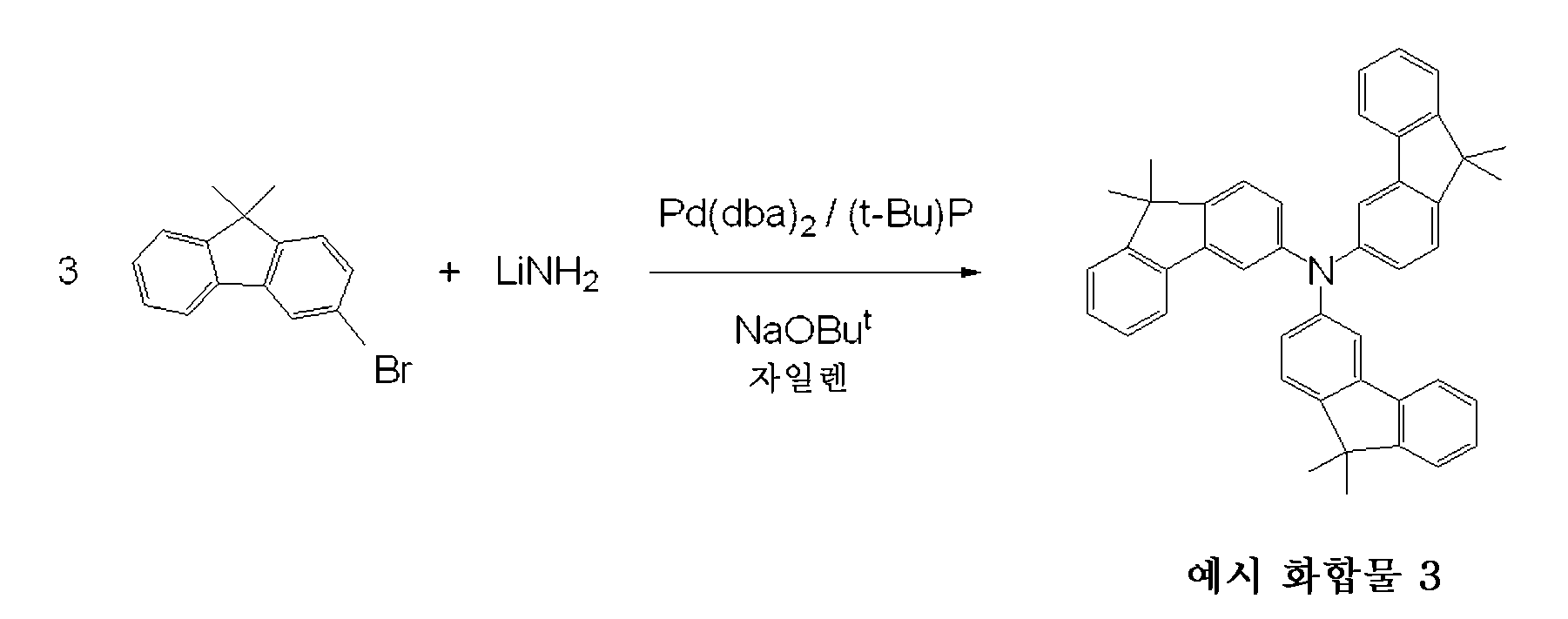
다음의 시약 및 용매를 100 ml 삼구 플라스크에 채웠다.The following reagents and solvents were charged into a 100 ml three-necked flask.
3-브로모플루오렌: 0.40 g (1.46 mmol)3-Bromofluorene: 0.40 g (1.46 mmol)
리튬 아미드 (상품명, 키시다 케미칼 코., 엘티디.에서 제조됨): 0.35 g (14.6 mmol)Lithium amide (trade name, manufactured by Kishida Chemical Co., Ltd.): 0.35 g (14.6 mmol)
나트륨 터트-부톡시드 (상품명, 도쿄 케미칼 인더스트리 코., 엘티디.에서 제조됨): 0.49 g (5.0 mmol)Sodium tert-butoxide (trade name, manufactured by Tokyo Chemical Industry Co., Ltd.): 0.49 g (5.0 mmol)
자일렌: 20 mlXylene: 20 ml
다음으로, 반응 용액을 질소 분위기하의 실온에서 휘저으면서, 트리-터트-부틸포스핀 (10 중량% 헥산 용액) 0.5 ml (0.15 mmol)을 첨가하였다. 그 후, 팔라듐 디벤질리덴아세톤 (상품명, 도쿄 케미칼 인더스트리 코., 엘티디.에서 제조됨) 0.67 mg (0.153 mmol)을 첨가하였다. 그 후, 플라스크 내에 아르곤을 도입해서 반응계를 아르곤으로 바꾼다. 그 후, 반응 용액을 가열 및 환류시키면서 6시간 휘저었다. 반응 완료 후, 반응 용액 중의 유기층을 톨루엔으로 수집하였다. 그 후, 유기층을 물로 세척하고, 무수 황산 나트륨에서 건조시키고, 용매를 감압하에서 증류하여 조 생성물을 얻었다. 그 후, 조 생성물을 실리카겔 칼럼 크로마토그래피 (전개 용매:헵탄/톨루엔 혼합 용매)에서 정제하여, 백색결정으로서 예시 화합물 3, 0.14 g (수율: 50.0%)을 얻었다.Next, 0.5 ml (0.15 mmol) of tri-tert-butylphosphine (10 wt% hexane solution) was added while the reaction solution was stirred at room temperature under a nitrogen atmosphere. Thereafter, 0.67 mg (0.153 mmol) of palladium dibenzylidene acetone (trade name, manufactured by Tokyo Chemical Industry Co., Ltd.) was added. Thereafter, argon was introduced into the flask, and the reaction system was changed to argon. Thereafter, the reaction solution was stirred for 6 hours while heating and refluxing. After completion of the reaction, the organic layer in the reaction solution was collected with toluene. Then, the organic layer was washed with water, dried over anhydrous sodium sulfate, and the solvent was distilled off under reduced pressure to obtain a crude product. Thereafter, the crude product was purified by silica gel column chromatography (developing solvent: heptane / toluene mixed solvent) to obtain 0.14 g (yield: 50.0%) of Exemplary Compound 3 as white crystals.
매트릭스 보조 레이저 탈착/이온화 비행시간형 질량분석기(MALDI-TOF MS)에 따라서, 예시 화합물 3의 M+인 593.0을 확인하였다.According to a matrix assisted laser desorption / ionization time-of-flight mass spectrometer (MALDI-TOF MS), 593.0 of the M + of Example Compound 3 was identified.
또한, 1H-NMR 측정에 의해, 예시 화합물 3의 구조를 확인하였다.Further, the structure of Example Compound 3 was confirmed by 1 H-NMR measurement.
1H-NMR (CDCl3, 400 MHz (제올 엘티디.에 의해 제조된 ECA-400으로 측정))σ (ppm): 7.56 (2H, dt), 7.42 (1H, dd), 7.32-7.25 (3H, m), 7.10 (1H, dd), 1.52 (6H, s) 1 H-NMR (CDCl 3, 400 MHz ( measured by ECA-400) manufactured by JEOL tidi El.) Σ (ppm): 7.56 (2H, dt), 7.42 (1H, dd), 7.32-7.25 (3H , m), 7.10 (1 H, dd), 1.52 (6 H, s)
이온화 포텐셜 등의 측정 및 평가Measurement and evaluation of ionization potential
상기 합성예 1 내지 3에서 합성한 예시 화합물 1 내지 3 및 후술하는 α-NPD의 이온화 포텐셜 등을 다음의 방법으로 평가하였다.The ionization potentials and the like of the
(1) 에너지 간격(1) Energy gap
박막으로 형성된 대상 화합물의 UV-가시 흡수 스펙트럼을 히타치 엘티디.에서 제조한 분광 광도계 U-3010을 이용하여 측정하였다. 박막은 유리 기판 상에서 대상 화합물을 성막함으로써 얻었다. 다음으로, 측정한 UV-가시 흡수 스펙트럼의 흡수 끝으로부터 에너지 간격을 측정하였다.The UV-visible absorption spectrum of the target compound formed as a thin film was measured using a spectrophotometer U-3010 manufactured by Hitachi, Ltd. The thin film was obtained by forming an object compound on a glass substrate. Next, the energy interval was measured from the absorption edge of the measured UV-visible absorption spectrum.
(2) 이온화 포텐셜(2) ionization potential
대기에서 광전자분광법 (측정기 이름 AC-1 리켄키키 코., 엘티디.에서 제조됨)을 이용해서 이온화 포텐셜을 측정하였다.The ionization potential was measured using photoelectron spectroscopy (instrument name AC-1 Riken Kikiko, manufactured by ELD.) In the atmosphere.
(3) 전자친화력(3) Electron affinity
다음의 계산식으로 전자친화력을 계산하였다:The electron affinity was calculated by the following equation:
[전자친화력] = [이온화 포텐셜] - [에너지 간격][Electron affinity] = [ionization potential] - [energy interval]
(4) 라디칼 양이온의 흡수 스펙트럼(4) Absorption spectrum of radical cation
다음의 분석 기기를 이용해서 라디칼 양이온의 흡수 스펙트럼을 측정 및 평가하였다.The absorption spectra of the radical cations were measured and evaluated using the following analytical instrument.
전기화학 분석기 (포텐시오스타트): ALS에서 제조된 660CElectrochemical analyzer (Potentiostat): 660C manufactured by ALS
흡수 스펙트럼의 측정용 광원: 오션 옵틱스에서 제조된 중수소 텅스텐 할로겐 광원 DH-2000Light source for measurement of absorption spectrum: Deuterium tungsten halogen light source DH-2000 manufactured by Ocean Optics
흡수 스펙트럼의 측정용 분광기: 오션 옵틱스에서 제조된 USB-2000Spectrometer for measurement of absorption spectrum: USB-2000 manufactured by Ocean Optics
우선 대상 화합물을 전해질 용매와 혼합하였다. 그 후 포텐시오스타트로 혼합 용액에 전압을 인가하여, 대상 화합물을 산화하고, 그 흡수 스펙트럼을 측정하였다. 혼합 용액의 대상 화합물의 농도는 1x10⁻² 내지 1x10⁻⁵ mol/l였다. 흡수 스펙트럼의 측정을 위해, 대상 화합물을 산화하기 위한 포텐셜을 혼합 용액에 인가하여, 흡수 스펙트럼의 시간에 따른 변화를 측정하였다. 이 측정에 의해 얻어지는 흡수 스펙트럼은, 중성상태 및 라디칼 양이온 상태에서 흡수 스펙트럼의 합이다. 전화(electrification) 전하량 (암페로메트리)으로부터 라디칼 양이온의 생성량을 추산할 수 있으므로, 중성 분자와 라디칼 양이온 사이의 존재비와, 중성 분자와 라디칼 양이온 모두의 흡수 스펙트럼으로부터, 라디칼 양이온 상태에서의 흡수 스펙트럼을 추출할 수 있다.First, the target compound was mixed with an electrolyte solvent. Thereafter, a voltage was applied to the mixed solution by potentiostat to oxidize the target compound, and the absorption spectrum thereof was measured. The concentration of the target compound in the mixed solution was 1 x 10 -2 to 1 x 10 -5 mol / l. For measurement of the absorption spectrum, a potential for oxidizing the target compound was applied to the mixed solution, and a change with time of the absorption spectrum was measured. The absorption spectrum obtained by this measurement is the sum of absorption spectra in a neutral state and a radical cation state. It is possible to estimate the amount of radical cation generated from the electrification charge amount (amperometry), so that the ratio of the abundance between the neutral molecule and the radical cation and the absorption spectrum of both the neutral molecule and the radical cation, Can be extracted.
도 2 내지 도 5는 각각 예시 화합물 1 내지 3 및 α-NPD의 중성상태 및 양이온 여기 상태에 있어서의 UV-가시 흡수 스펙트럼을 나타내는 도면이다. 도 2 내지 도 5 각각에서, 중성상태에 있어서의 UV-가시 흡수 스펙트럼은 1로 나타내어지고, 양이온 여기 상태에 있어서의 UV-가시 흡수 스펙트럼은 2로 나타내어 진다.Figs. 2 to 5 are diagrams showing UV-visible absorption spectra in the neutral state and the cation-excited state of Exemplified Compounds 1 to 3 and? -NPD, respectively. 2 to 5, the UV-visible absorption spectrum in the neutral state is represented by 1 and the UV-visible absorption spectrum in the cation-excited state is represented by 2.
(실시예 1)(Example 1)
기판 상에, 애노드, 정공 수송층, 발광층, 전자 수송층 및 캐소드가 이 순서대로 적층되어 있는 유기 발광 소자를, 다음의 방법으로 생산하였다.An organic luminescent element in which an anode, a hole transporting layer, a luminescent layer, an electron transporting layer and a cathode were laminated in this order on a substrate was produced by the following method.
(1) 사용한 화합물 및 그 합성법(1) Compound used and synthesis method thereof
본 실시예에서 정공 수송층, 발광층 및 전자 수송층의 어느 하나에 대한 구성 재료로서 사용한 화합물의 일부를 아래에 나타낸다.Some of the compounds used as constituent materials for the hole transporting layer, the light emitting layer and the electron transporting layer in this embodiment are shown below.
<화학식>≪

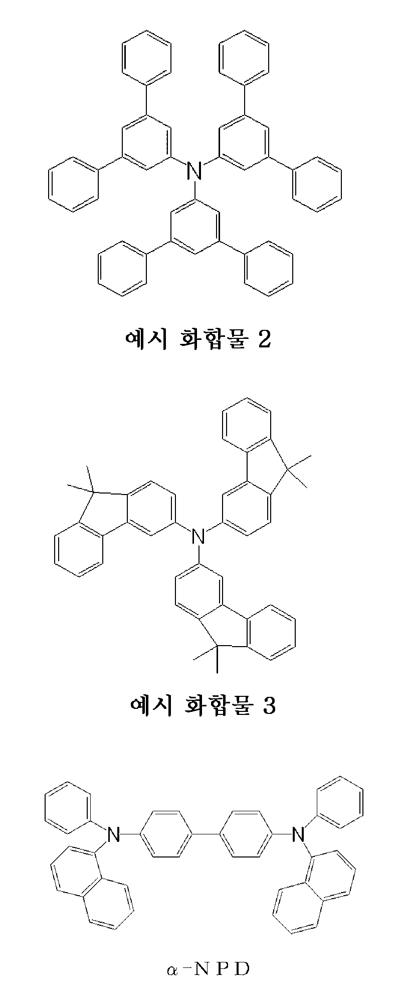
이하, 본 실시예에서 사용한 화합물의 합성법을 아래에 나타낸다.Hereinafter, the synthesis method of the compound used in this embodiment is shown below.
(i) 화합물 A1 (호스트)(i) Compound A1 (host)
다음의 합성 기법에 의해 화합물 A1을 합성하였다.Compound A1 was synthesized by the following synthesis technique.
<반응식><Reaction Scheme>

(i-1) 다음의 시약 및 용매를 500 ml 삼구 플라스크에 채웠다.(i-1) The following reagents and solvents were charged into a 500 ml three-necked flask.
2,7-디브로모-9,9-디메틸플루오렌 (화합물 a): 2.0 g (5.68 mmol)2,7-dibromo-9,9-dimethylfluorene (Compound a): 2.0 g (5.68 mmol)
피렌-1-보론산 (화합물 b): 4.2 g (17.0 mmol)Pyrene-1-boronic acid (compound b): 4.2 g (17.0 mmol)
톨루엔: 120 ml Toluene: 120 ml
에탄올: 60 mlEthanol: 60 ml
다음으로, 반응계 내를 질소분위기로 바꾼 후, 반응 용액을 실온에서 휘저으면서, 탄산 나트륨 24 g 및 물 120 ml을 혼합한 수용액을 떨어뜨리고, 다음에 테트라키스(트리페닐포스핀)팔라듐(0) 0.33 g (0.28 mmol)을 용액에 첨가하였다. 그 후, 반응 용액을 실온에서 30분 휘젓고, 77℃로 가열하고, 이 온도(77℃)에서 5시간 휘저었다. 반응 완료 후, 유기층을 클로로포름으로 추출하고, 무수황산나트륨에서 건조시킨 후에, 용매를 감압하에서 증류하여 조 생성물을 얻었다. 다음으로, 조 생성물을 실리카겔 칼럼 크로마토그래피 (전개 용매: 헥산/톨루엔 혼합 용매)로 정제하여, 백색 결정으로서 화합물 c, 3.0 g (수율: 89.0%)을 얻었다.Next, an aqueous solution obtained by mixing 24 g of sodium carbonate and 120 ml of water was dropped while stirring the reaction solution at room temperature, and then tetrakis (triphenylphosphine) palladium (0) was added thereto. 0.33 g (0.28 mmol) was added to the solution. Thereafter, the reaction solution was stirred at room temperature for 30 minutes, heated to 77 占 폚, and stirred at this temperature (77 占 폚) for 5 hours. After completion of the reaction, the organic layer was extracted with chloroform, dried over anhydrous sodium sulfate, and then the solvent was distilled off under reduced pressure to obtain a crude product. Subsequently, the crude product was purified by silica gel column chromatography (developing solvent: hexane / toluene mixed solvent) to obtain 3.0 g (yield: 89.0%) of compound c as white crystals.
(i-2) 다음의 시약 및 용매를 500 ml 삼구 플라스크에 채웠다.(i-2) The following reagents and solvents were charged into a 500 ml three-necked flask.
화합물 c: 3.51 g (5.89 mmol)Compound c: 3.51 g (5.89 mmol)
터트-부틸 클로라이드: 1.64 g (17.67 mmol)Tert-butyl chloride: 1.64 g (17.67 mmol)
디클로로메탄: 200 mlDichloromethane: 200 ml
다음으로, 반응 용액을 0℃로 냉각한 후, 이 온도(0℃)에서 휘저으면서 염화 알루미늄 1.71 g (13.0 mmol)을 소량씩 첨가하였다. 그 후, 반응 용액을 이 온도(0℃)에서 30분 휘젓고, 실온으로 가열하고, 5시간 더 휘저었다. 반응 완료 후, 반응 용액을 물 200 ml에 붓고, 그 후 유기층을 클로로포름으로 추출하고, 무수황산나트륨에서 건조시켰다. 다음으로, 용매를 감압하에서 증류하여 조 생성물을 얻었다. 조 생성물을 실리카겔 칼럼 크로마토그래피 (전개 용매: 헥산/톨루엔 혼합 용매)로 정제하여, 백색 결정으로서 화합물 A1, 3.53 g (수율: 84%)을 얻었다.Next, the reaction solution was cooled to 0 캜, and 1.71 g (13.0 mmol) of aluminum chloride was added in small portions while stirring at this temperature (0 캜). Thereafter, the reaction solution was stirred at this temperature (0 ° C) for 30 minutes, heated to room temperature, and further stirred for 5 hours. After completion of the reaction, the reaction solution was poured into 200 ml of water, and then the organic layer was extracted with chloroform and dried over anhydrous sodium sulfate. Next, the solvent was distilled off under reduced pressure to obtain a crude product. The crude product was purified by silica gel column chromatography (developing solvent: hexane / toluene mixed solvent) to obtain 3.53 g (yield: 84%) of Compound A1 as white crystals.
(ii) 화합물 A2 (발광 도펀트)(ii) Compound A2 (luminescent dopant)
다음의 합성 기법에 의해 화합물 A2을 합성하였다.Compound A2 was synthesized by the following synthesis technique.
<반응식><Reaction Scheme>

다음의 시약 및 용매를 200 ml 삼구 플라스크에 채웠다.The following reagents and solvents were charged into a 200 ml three-necked flask.
화합물 d: 0.924 g (1.70 mmol)Compound d: 0.924 g (1.70 mmol)
화합물 e: 0.957 g (3.40 mmol)Compound e: 0.957 g (3.40 mmol)
나트륨 터트-부톡사이드: 0.65 g (6.80 mmol)Sodium tert-butoxide: 0.65 g (6.80 mmol)
자일렌: 100 mlXylene: 100 ml
다음으로, 반응계 내를 질소분위기로 바꾼 후, 반응 용액을 실온에서 휘저으면서, 다음의 시약을 순차적으로 첨가했다.Next, the inside of the reaction system was changed to a nitrogen atmosphere, and the following reagents were sequentially added while stirring the reaction solution at room temperature.
트리-(터트-부틸)포스핀: 34.4 mg (0.17 mmol)Tri- (tert-butyl) phosphine: 34.4 mg (0.17 mmol)
팔라듐 디벤질리덴아세톤: 48.9 mg (0.085 mmol)Palladium dibenzylidene acetone: 48.9 mg (0.085 mmol)
다음으로, 반응 용액을 125℃로 가열하고, 이 온도(125℃)에서 3시간 휘저었다. 반응 완료 후, 유기층을 톨루엔으로 추출하고 무수황산나트륨에서 건조시켰다. 다음으로, 용매를 감압하에서 증류하여 조 생성물을 얻었다. 조 생성물을 실리카겔 칼럼 크로마토그래피 (전개 용매: 헵탄/톨루엔 혼합 용매)로 정제하여, 황백색 결정으로서 화합물 A2, 0.920 g (수율: 72.7%)을 얻었다.Next, the reaction solution was heated to 125 DEG C and stirred at this temperature (125 DEG C) for 3 hours. After completion of the reaction, the organic layer was extracted with toluene and dried over anhydrous sodium sulfate. Next, the solvent was distilled off under reduced pressure to obtain a crude product. The crude product was purified by silica gel column chromatography (developing solvent: heptane / toluene mixed solvent) to obtain 0.920 g (yield: 72.7%) of Compound A2 as yellowish white crystals.
질량분석법에 의해, 화합물의 M+인 743.5을 확인하였다. 또한, 시차 주사 열량분석기(DSC)에 의해, 화합물의 융점이 323℃인 것을 확인하였다.Mass spectrometry confirmed the M + of the compound 743.5. Further, it was confirmed by a differential scanning calorimeter (DSC) that the melting point of the compound was 323 ° C.
(iii) 화합물 A3 (정공 수송성 재료)(iii) Compound A3 (hole transporting material)
다음의 합성 기법에 의해 화합물 A3을 합성하였다.Compound A3 was synthesized by the following synthesis technique.
<화학식>≪
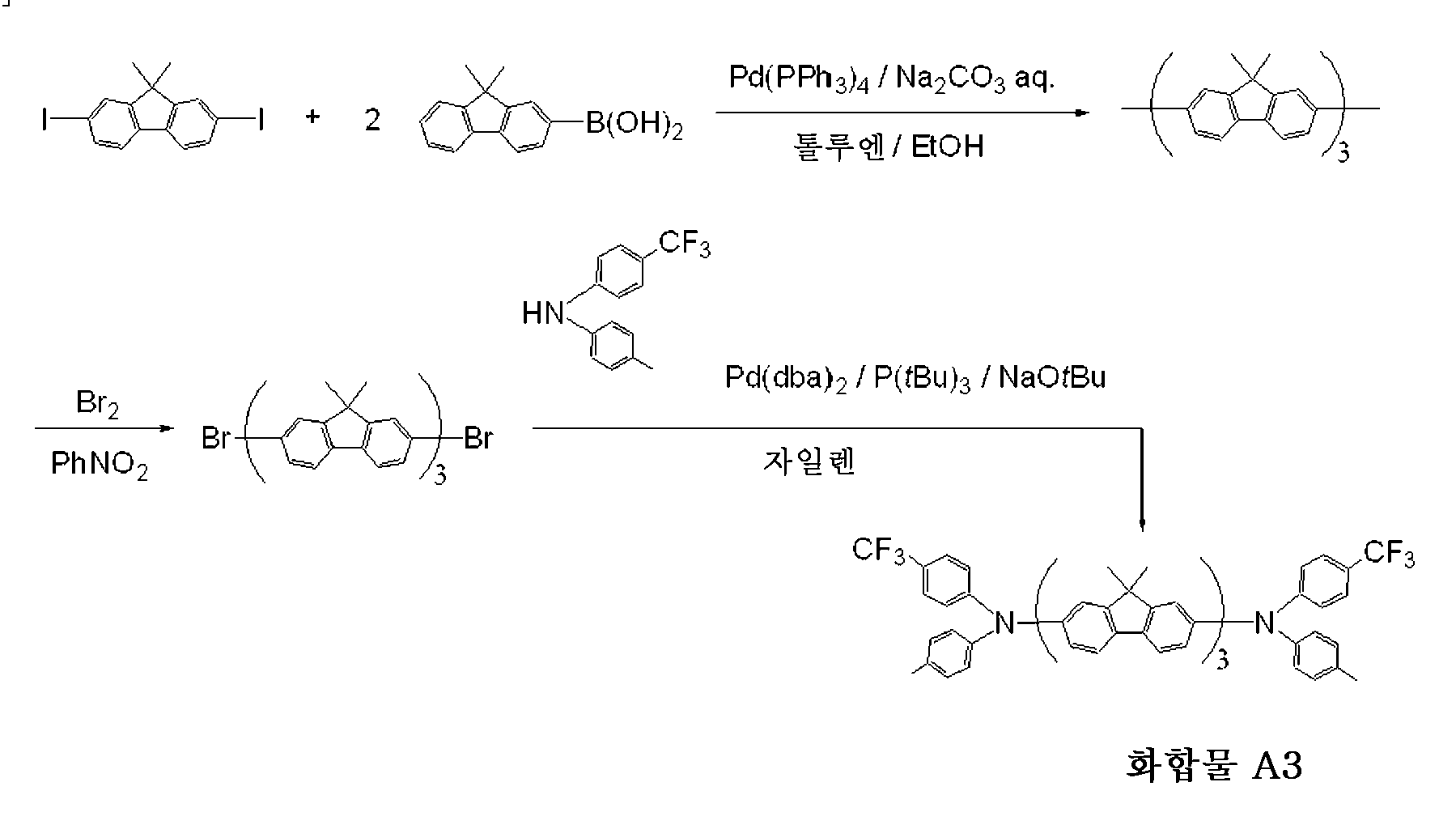
(iii-1) 반응 용기 내로 질소를 도입함으로써 반응계 내를 질소분위기하에서 유지하면서, 반응 용기에 다음의 시약과 용매를 채웠다.(iii-1) While maintaining the inside of the reaction system under a nitrogen atmosphere by introducing nitrogen into the reaction vessel, the following reagents and solvent were charged into the reaction vessel.
2,7-디요오도-9,9-디메틸플루오렌: 5 g (11.2 mmol)2,7-diiodo-9,9-dimethylfluorene 5 g (11.2 mmol)
9,9-디메틸플루오렌-2-보론산: 9 g (24.7 mmol)9,9-Dimethylfluorene-2-boronic acid: 9 g (24.7 mmol)
톨루엔(탈기): 200 mlToluene (degassing): 200 ml
에탄올: 100 mlEthanol: 100 ml
다음으로, 실온에서 반응 용액을 휘저으면서, 무수 탄산 나트륨 51 g 및 물 250 ml를 혼합하여 제조한 탄산 나트륨 수용액 245 ml을 떨어뜨렸다. 그 후, 반응 용액을 실온에서 30분 휘젓고 그 후, 테트라키스(트리페닐포스핀)팔라듐 142 g (1.23 mmol)을 용액에 첨가하였다. 그 후, 80℃로 가열한 오일 배스 상에서 반응 용기를 가열하면서, 반응 용액을 약 3시간 가열하며 휘저었다. 반응 용액을 실온으로 되돌린 후, 물 100 ml 및 에틸 아세테이트 100 ml를 용액에 첨가하였다. 그 후, 용매 추출 (제1 용매 추출)에 의해 용액을 물층과 유기층을 분리하여 유기층을 수집하였다. 그 후, 물층에 톨루엔 및 아세트산 에틸을 첨가하고, 용매 추출 (제2 용매 추출)에 의해 용액을 물층과 유기층으로 분리해서 유기층을 수집하였다. 그 후, 제1 및 제2 용매 추출에서 수집한 유기층을 황산 나트륨에서 건조시켰다. 다음으로, 용매를 감압하에서 증류하여 조 생성물을 얻었다. 조 생성물을 실리카겔 칼럼 크로마토그래피 (전개 용매: 톨루엔:헵탄=1:2)로 정제하여, 2,2':7',2"-트리스(9,9-디메틸플루오렌) 4.9 g을 얻었다.Next, while stirring the reaction solution at room temperature, 245 ml of an aqueous sodium carbonate solution prepared by mixing 51 g of anhydrous sodium carbonate and 250 ml of water was dropped. The reaction solution was then stirred at room temperature for 30 minutes, after which 142 g (1.23 mmol) of tetrakis (triphenylphosphine) palladium was added to the solution. Thereafter, while heating the reaction vessel on an oil bath heated to 80 DEG C, the reaction solution was heated for about 3 hours and agitated. After the reaction solution was returned to room temperature, 100 ml of water and 100 ml of ethyl acetate were added to the solution. Thereafter, the solution was separated from the water layer and the organic layer by solvent extraction (first solvent extraction), and the organic layer was collected. Thereafter, toluene and ethyl acetate were added to the water layer, and the organic layer was collected by separating the solution into an aqueous layer and an organic layer by solvent extraction (second solvent extraction). The organic layer collected in the first and second solvent extraction was then dried over sodium sulfate. Next, the solvent was distilled off under reduced pressure to obtain a crude product. The crude product was purified by silica gel column chromatography (developing solvent: toluene: heptane = 1: 2) to obtain 4.9 g of 2,2 ': 7', 2 "-tris (9,9-dimethylfluorene).
(iii-2) 반응 용기 내로 질소를 도입함으로써 반응계 내를 질소분위기하에서 유지하면서, 반응 용기에 다음의 시약과 용매를 채웠다. 다음의 시약 및 용매는 반응 용기를 가열하면서 혼합했다.(iii-2) The reaction vessel was charged with the following reagents and solvent while maintaining the inside of the reaction system under a nitrogen atmosphere by introducing nitrogen into the reaction vessel. The following reagents and solvents were mixed while heating the reaction vessel.
2,2':7',2"-트리스(9,9-디메틸플루오렌): 4.5 g (7.79 mmol)2,2 ': 7', 2 "-tris (9,9-dimethylfluorene): 4.5 g (7.79 mmol)
니트로벤젠: 150 mlNitrobenzene: 150 ml
다음으로, 60℃로 가열한 오일 배스 상에서 반응 용기를 가열하면서, 브롬 2.5 g (15.6 mmol)을 천천히 떨어뜨린 후, 약 2시간 더 휘저었다. 그 후, 반응 용기를 아이스 배스에 옮겼다. 반응 용액을 냉각하면서, 잠시 휘젓고 그 후 침전물을 여과하였다. 침전물을 톨루엔으로 재결정 한 후, 여과, 건조하여 7,7"-디브로모-2,2':7',2"-트리스(9,9-디메틸플루오렌) 3.4 g을 얻었다.Next, 2.5 g (15.6 mmol) of bromine was slowly dropped while the reaction vessel was heated on the oil bath heated to 60 占 폚, and the mixture was further stirred for about 2 hours. Thereafter, the reaction vessel was transferred to an ice bath. While the reaction solution was cooled, it was stirred for a while, and then the precipitate was filtered. The precipitate was recrystallized from toluene, filtered and dried to obtain 3.4 g of 7,7 "-dibromo-2,2 ': 7', 2" -tris (9,9-dimethylfluorene).
(iii-3) 반응 용기 내로 질소를 도입함으로써 반응계 내를 질소분위기하에서 유지하면서, 반응 용기에 다음의 시약과 용매를 채웠다.(iii-3) While maintaining the inside of the reaction system under a nitrogen atmosphere by introducing nitrogen into the reaction vessel, the reaction vessel was filled with the following reagents and solvent.
팔라듐 비스(벤질리덴아세톤): 156 mg (0.272 mmol)Palladium bis (benzylideneacetone): 156 mg (0.272 mmol)
트리-터트-부틸포스핀: 330 mg (1.63 mmol)Tri-tert-butylphosphine: 330 mg (1.63 mmol)
자일렌: 20 mlXylene: 20 ml
다음으로, 실온에서 반응 용액을 15분간 휘저었다. 그 후, 자일렌 50 ml 및 7,7"-디브로모-2,2':7',2"-트리스(9,9-디메틸플루오렌) 1 g (1.36 mmol)을 혼합해서 제조한 자일렌 용액을 상기 자일렌 용액에 떨어뜨렸다. 반응 용기를 50℃로 가열한 오일 배스 상에서 가열하면서 반응 용액을 30분 휘저었다. 그 후, N-(4-트리플루오로메틸페닐)-N-(4-메틸페닐)아민 1.08 g (4.08 mmol)과 자일렌 20 ml를 혼합해서 제조한 자일렌 용액을 반응 용액에 떨어뜨렸다. 그 후, 반응 용액에 나트륨 터트-부톡사이드 588 mg (6.12 mmol)을 첨가하였다. 다음으로, 반응 용기를 130℃로 가열한 오일 배스 상에서 약 5시간 가열하고, 휘저었다. 반응 용액을 실온으로 되돌린 후, 물 50 ml를 용액에 첨가하였다. 그 결과로 생성된 반응 용액을 제1 용매 추출로 물층과 유기층으로 분리하였다. 그 후, 물층에 톨루엔 및 에틸 아세테이트를 가하고, 제2 용매 추출로 용액을 물층과 유기층으로 분리하였다. 다음으로, 제1 및 제2 용매 추출에서 수집한 유기층을 황산 마그네슘에서 건조시켰다. 용매를 감압하에서 증류하여 조 생성물을 얻었다. 조 생성물을 실리카겔 칼럼 크로마토그래피 (톨루엔:헵탄=1:2)로 정제하고, 화합물 A3, 1.2g을 얻었다.Next, the reaction solution was stirred at room temperature for 15 minutes. Thereafter, 50 ml of xylene and 1 g (1.36 mmol) of 7,7-dibromo-2,2 ': 7', 2 "-tris (9,9-dimethylfluorene) The solution of phenol was dropped into the xylene solution. The reaction vessel was heated on an oil bath heated to 50 DEG C while stirring the reaction solution for 30 minutes. Thereafter, a xylene solution prepared by mixing 1.08 g (4.08 mmol) of N- (4-trifluoromethylphenyl) -N- (4-methylphenyl) amine and 20 ml of xylene was dropped into the reaction solution. Then, 588 mg (6.12 mmol) of sodium tert-butoxide was added to the reaction solution. Next, the reaction vessel was heated on an oil bath heated to 130 DEG C for about 5 hours and agitated. After the reaction solution was returned to room temperature, 50 ml of water was added to the solution. The resultant reaction solution was separated into a water layer and an organic layer by a first solvent extraction. Then, toluene and ethyl acetate were added to the water layer, and the solution was separated into an aqueous layer and an organic layer by a second solvent extraction. Next, the organic layer collected in the first and second solvent extraction was dried over magnesium sulfate. The solvent was distilled off under reduced pressure to obtain a crude product. The crude product was purified by silica gel column chromatography (toluene: heptane = 1: 2) to obtain 1.2 g of Compound A3.
매트릭스 보조 레이저 탈착/이온화 비행시간형 질량분석기(MALDI-TOF MS)에 따라서, 예시 화합물 A3의 M+인 1076을 확인하였다.According to the matrix assisted laser desorption / ionization time-of-flight mass spectrometry (MALDI-TOF MS), the M + of Example Compound A3, 1076, was identified.
(2) 유기 발광 소자의 제작 방법(2) Manufacturing method of organic light emitting device
우선 스퍼터링으로, 유리 기판 (기판) 상에 인듐 산화 주석(ITO)을 성막하여, 애노드를 형성하였다. 애노드의 막 두께는 120 nm로 두었다. 그 후, 애노드가 형성되어 있는 기판을, 아세톤 및 이소프로필 알콜(IPA)로 순차적으로 초음파 세척하고, IPA로 끓여 세척한 후, 건조하였다. 그 후, 기판을 UV/오존 세척하였다. 이렇게 처리한 기판을 유기 발광 소자의 제조를 위한 투명도전성 지지 기판으로 사용하였다.First, indium tin oxide (ITO) was deposited on a glass substrate (substrate) by sputtering to form an anode. The thickness of the anode was set at 120 nm. Subsequently, the substrate on which the anode was formed was sequentially ultrasonically washed with acetone and isopropyl alcohol (IPA), boiled with IPA, washed, and then dried. Thereafter, the substrate was subjected to UV / ozone cleaning. The substrate thus treated was used as a transparent conductive support substrate for the production of an organic light emitting device.
다음으로, 화합물 A3 (이온화 포텐셜: 5.85 eV) 및 예시 화합물 1 (이온화 포텐셜: 5.46 eV)를 10:1의 질량비를 갖도록 혼합하였다. 그 후, 혼합물을 클로로포름과 혼합하여, 1 중량%의 클로로포름 용액을 제조하였다. 다음으로, 클로로포름 용액을 애노드에 떨어뜨리고, 최초로 회전수 500 RPM으로 10초, 그 후 회전수 1000 RPM으로 40초 스핀 코팅하여, 정공 수송층의 역할을 하는 박막을 형성하였다. 정공 수송층의 두께는 11 nm이었다.Next, Compound A3 (ionization potential: 5.85 eV) and Exemplified Compound 1 (ionization potential: 5.46 eV) were mixed with a mass ratio of 10: 1. Thereafter, the mixture was mixed with chloroform to prepare a 1 wt% chloroform solution. Next, the chloroform solution was dropped on the anode, and spin-coated for the first time at a number of revolutions of 500 rpm for 10 seconds and then at a number of revolutions of 1000 rpm for 40 seconds to form a thin film serving as a hole transport layer. The thickness of the hole transport layer was 11 nm.
다음으로, 진공증착으로, 정공 수송층 상에 호스트 화합물 A1 및 발광 도펀트로서 화합물 A2를, 그 층의 화합물 A2의 농도가 5 중량%로 되도록 함께 증착함으로써 발광층을 형성하였다. 발광층의 막 두께는 100 nm로 두었고, 호스트 및 도펀트의 성막 속도는 각각 0.1 nm/초, 0.01 nm/초로 두고, 증착시의 진공도는 5.0x10⁻⁵ Pa로 두었다.Next, a host compound A1 and a compound A2 as a luminescent dopant were vapor-deposited on the hole transporting layer together with a vacuum evaporation deposition so that the concentration of the compound A2 in the layer was 5% by weight, thereby forming a light emitting layer. The film thickness of the light emitting layer was set to 100 nm, the deposition rates of the host and the dopant were set to 0.1 nm / second and 0.01 nm / second, respectively, and the degree of vacuum during deposition was set to 5.0 × 10 -5 Pa.
다음으로, 진공증착으로, 발광층 상에, 나드(NARD) 인스티튜트 엘티디.에 의해 제조된 바소페난트롤린 (BPhen)을 성막하여 전자 수송층을 형성하였다. 전자 수송층의 두께는 20 nm로 두었고, 증착시의 진공도는 5.0x10⁻⁵ Pa로 두었으며, 성막 속도는 0.1 nm/초로 두었다.Next, on the light-emitting layer, by vacuum deposition, a film of barophenanthroline (BPhen) produced by NARD Institute Inc. was formed to form an electron transporting layer. The thickness of the electron transport layer was set to 20 nm, the degree of vacuum during deposition was set to 5.0 x 10 -5 Pa, and the deposition rate was set to 0.1 nm / sec.
다음으로, 진공증착으로, 전자 수송층 상에, 알루미늄-리튬 합금 (리튬 농도 1 at%)으로 이루어지는 증착 재료를 성막하여, 합금 박막을 형성하였다. 합금 박막의 두께는 0.5 nm로 두었다. 그 후, 진공증착으로 이전에 형성한 합금 박막 상에, 알루미늄을 성막하여 Al 박막을 형성하였다. Al 박막의 두께는 150 nm로 두었다. 금속 박막 및 Al 박막은 전자 주입 전극 (캐소드)로서 기능한다. 또한, 금속 박막 및 Al 박막을 형성할 때, 증착시의 진공도는 5.0x10⁻⁵ Pa로 두었고, 성막 속도는 1.0 내지 1.2 nm/초로 두었다.Next, an evaporation material made of an aluminum-lithium alloy (
다음으로, 이렇게 얻어진 소자를 소자가 수분을 흡착하여 그의 발광 강도가 저하되지 않도록, 질소분위기에서 보호용 유리 판으로 덮고, 에폭시 수지계 접착재로 밀봉하였다. 사용한 보호용 유리의 접착 표면은 수분흡착용의 시트(다이닉 코., 엘티디.에서 제조된 유기 EL 용 수분 목적 시트)가 제공되었다.Next, the thus-obtained device was covered with a protective glass plate in a nitrogen atmosphere so that the device adsorbs moisture and its light emission intensity is not lowered, and is sealed with an epoxy resin-based adhesive. The adhesive surface of the used protective glass was provided with a sheet for moisture adsorption (moisture objective sheet for organic EL manufactured by Denico Co., Ltd.).
이에 따라, 유기 발광 소자를 얻었다.Thus, an organic light emitting element was obtained.
전류를 이로 얻어진 소자에 인가하는 경우, 소자는 청색 발광을 나타내었다. 청색의 최대 방출 파장은 460 nm이었다. 또한, 33 mA/cm2의 전류를 유지하면서 소자에 연속적으로 전압을 인가함으로써 소자의 수명을 평가하였다. 구체적으로 전압의 연속 인가에 의한 초기 휘도의 반감기를 평가하였다. 표 3은 그 결과를 나타낸다.When a current was applied to the resulting device, the device showed blue light emission. The maximum emission wavelength of blue was 460 nm. In addition, the lifetime of the device was evaluated by continuously applying a voltage to the device while maintaining a current of 33 mA / cm < 2 & gt ;. Specifically, the half-life period of the initial luminance by continuous application of voltage was evaluated. Table 3 shows the results.
(실시예 2)(Example 2)
정공 수송층의 구성 재료로 예시 화합물 1 대신에, 예시 화합물 2 (이온화 포텐셜: 5.72 eV)를 이용하는 것을 제외하고는, 실시예 1의 것과 같은 방법에 의해 유기 발광 소자를 제조하였다. 얻어진 소자는 실시예 1과 같은 방법으로 평가하였다. 표 3은 그 결과를 나타낸다.An organic luminescent device was produced in the same manner as in Example 1, except that Exemplified Compound 2 (ionization potential: 5.72 eV) was used instead of
(실시예 3)(Example 3)
정공 수송층의 구성 재료로 예시 화합물 1 대신에, 예시 화합물 3 (이온화 포텐셜: 5.51 eV)을 이용하는 것을 제외하고는, 실시예 1의 것과 같은 방법에 의해 유기 발광 소자를 제조하였다. 얻어진 소자는 실시예 1과 같은 방법으로 평가를 행하였다. 표 3은 그 결과를 나타낸다.An organic luminescent device was produced in the same manner as in Example 1, except that Exemplified Compound 3 (ionization potential: 5.51 eV) was used instead of
(비교예 1)(Comparative Example 1)
정공 수송층의 구성 재료로 예시 화합물 1 대신에, 다음의 화학식으로 나타내어지는 α-NPD (이온화 포텐셜: 5.40 eV)을 이용하는 것을 제외하고는, 실시예 1의 것과 같은 방법에 의해 유기 발광 소자를 제조하였다. 얻어진 소자는 실시예 1과 같은 방법으로 평가를 행하였다. 표 3은 그 결과를 나타낸다.An organic luminescent device was produced in the same manner as in Example 1, except that? -NPD (ionization potential: 5.40 eV) represented by the following formula was used instead of
<화학식>≪
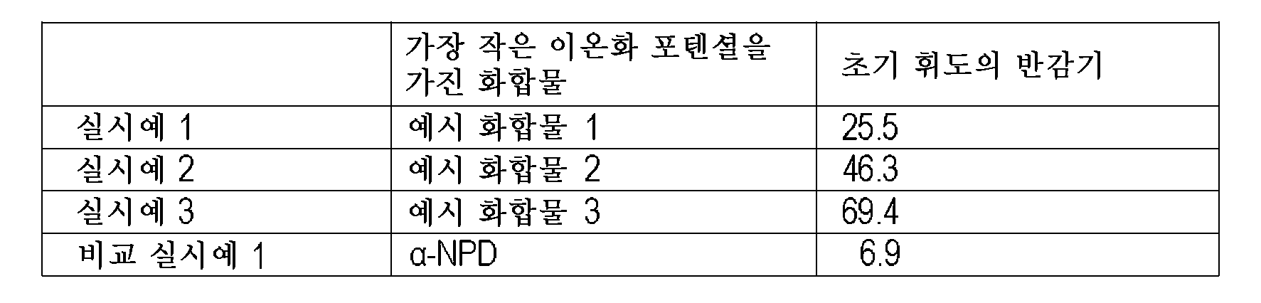
표 3으로부터, 실시예 1 내지 3의 유기 발광 소자는 비교예 1의 소자와 비교하여 초기 휘도의 반감기가 현저하게 향상되었다는 것을 알았다. 이것은 아마도 비교예 1로 사용한 α-NPD가 정공을 포함하여 라디칼 양이온 상태로 되었을 때, 발광층으로부터 발광되는 청색 발광 에너지의 일부를 흡수하여 화합물 자체의 구조가 변화하기 때문으로 생각된다. 한편, 실시예 1 내지 3에서 각각 사용된 예시 화합물 1 내지 3은 정공을 포함하여 라디칼 양이온 상태로 되었을 때, α-NPD에서 보는 바와 같은 구조의 변화는 일어나지 않는 것으로 생각된다.From Table 3, it was found that the half-life of the initial luminance was remarkably improved in the organic luminescent devices of Examples 1 to 3 as compared with the device of Comparative Example 1. [ This is presumably because the structure of the compound itself is presumably changed by absorbing a part of the blue light emission energy emitted from the light emitting layer when? -NPD used in Comparative Example 1 contains a hole and becomes a radical cation state. On the other hand, it is considered that the exemplified
도 2 내지 도 4에 도시된 바와 같이, 예시 화합물 1 내지 3은 라디칼 양이온 상태에서 청색 파장 영역 (410 nm 내지 490 nm)에 흡수 피크를 갖지 않는다. 한편, 도 5에 도시된 바와 같이, α-NPD는 라디칼 양이온 상태에서 청색 파장 영역(410 nm 내지 490 nm)에 흡수 피크를 갖는다.As shown in Figs. 2 to 4, Exemplary Compounds 1-3 do not have an absorption peak in the blue wavelength region (410 nm to 490 nm) in the radical cation state. On the other hand, as shown in FIG. 5,? -NPD has an absorption peak in the blue wavelength region (410 nm to 490 nm) in the radical cation state.
앞서 설명한 바와 같이, 실시예 1 내지 3의 유기 발광 소자는 연속 구동시에 내구성이 향상된다.As described above, the organic light emitting devices of Examples 1 to 3 have improved durability at the time of continuous operation.
산업상 이용가능성Industrial availability
본 발명에 따르면, 연속 구동시에 향상된 내구성을 갖는 유기 발광 소자를 제공할 수 있다.According to the present invention, it is possible to provide an organic light emitting device having improved durability at the time of continuous casting.
본 발명은 예시적인 실시양태를 참고로 설명되었지만, 본 발명이 개시된 예시적인 실시양태로 제한되는 것이 아니라는 것을 이해할 것이다. 다음의 청구항의 범위는 모든 그러한 변형 및 균등 구조 및 기능을 포함하도록 가장 넓은 해석으로 부여될 것이다.While the present invention has been described with reference to exemplary embodiments, it is to be understood that the invention is not limited to the disclosed exemplary embodiments. The scope of the following claims is to be accorded the broadest interpretation so as to encompass all such modifications and equivalent structures and functions.
이 출원은 그 전체가 여기에서 참고로 본원에 포함되어 있는 2009년 12월 14일에 출원된 일본 특허 출원 제2009-282648호의 이점을 주장한다.This application claims the benefit of Japanese Patent Application No. 2009-282648, filed December 14, 2009, the entirety of which is incorporated herein by reference.
Claims (10)
캐소드; 및
상기 애노드 및 상기 캐소드 사이에 배치되어, 적어도 정공 수송층 및 발광층을 포함하는 유기 화합물층을 포함하고:
여기서, 상기 발광층이 청색 발광 재료를 포함하고;
상기 정공 수송층이 복수 종류의 유기 화합물을 포함하고;
상기 유기 화합물 중 가장 작은 이온화 포텐셜을 갖는 유기 화합물이 라디칼 양이온 상태에서 청색 파장 영역에 흡수 스펙트럼 피크가 존재하지 않는 화합물을 포함하고;
가장 작은 이온화 포텐셜을 갖는 상기 유기 화합물이 다음의 일반 화학식 (1)로 표현되는 것인 유기 발광 소자.
<화학식>
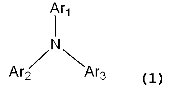
(Ar1 내지 Ar3이 각각 융합 다환 방향족기 또는 다음의 일반 화학식 (2)로 나타나는 치환 페닐 기를 나타내고(단, Ar1 내지 Ar3은 각각 다른 치환 기와 같아도 되고 상이해도 된다),
<화학식>

일반 화학식 (2)에 있어서, R1 및 R3은 각각 수소 원자, 할로겐 원자, 치환 혹은 비치환의 알킬기 또는 치환 혹은 비치환의 아릴기를 나타내며(단, R1 및 R3 중 어느 하나는 치환 혹은 비치환의 아릴기를 나타낸다); R2은 수소 원자, 할로겐 원자또는 치환 혹은 비치환의 알킬기이다)Anode;
Cathode; And
And an organic compound layer disposed between the anode and the cathode, the organic compound layer including at least a hole transporting layer and a light emitting layer,
Here, the light emitting layer includes a blue light emitting material;
Wherein the hole transport layer comprises a plurality of kinds of organic compounds;
Wherein the organic compound having the smallest ionization potential among the organic compounds has no absorption spectrum peak in the blue wavelength region in the radical cation state;
Wherein the organic compound having the lowest ionization potential is represented by the following general formula (1).
≪
(Wherein Ar 1 to Ar 3 each represent a fused polycyclic aromatic group or a substituted phenyl group represented by the following general formula (2) (provided that Ar 1 to Ar 3 may be the same as or different from each other)
≪
In the general formula (2), R 1 and R 3 each represent a hydrogen atom, a halogen atom, a substituted or unsubstituted alkyl group or a substituted or unsubstituted aryl group (provided that any of R 1 and R 3 is a substituted or unsubstituted An aryl group); R 2 is a hydrogen atom, a halogen atom or a substituted or unsubstituted alkyl group)
Applications Claiming Priority (3)
| Application Number | Priority Date | Filing Date | Title |
|---|---|---|---|
| JP2009282648A JP5675085B2 (en) | 2009-12-14 | 2009-12-14 | Organic light emitting device |
| JPJP-P-2009-282648 | 2009-12-14 | ||
| PCT/JP2010/072061 WO2011074461A1 (en) | 2009-12-14 | 2010-12-02 | Organic light emitting device |
Related Child Applications (1)
| Application Number | Title | Priority Date | Filing Date |
|---|---|---|---|
| KR1020147023485A Division KR20140110098A (en) | 2009-12-14 | 2010-12-02 | Organic light emitting device |
Publications (2)
| Publication Number | Publication Date |
|---|---|
| KR20120101114A KR20120101114A (en) | 2012-09-12 |
| KR101503986B1 true KR101503986B1 (en) | 2015-03-18 |
Family
ID=44167218
Family Applications (2)
| Application Number | Title | Priority Date | Filing Date |
|---|---|---|---|
| KR1020127017690A Active KR101503986B1 (en) | 2009-12-14 | 2010-12-02 | Organic light emitting device |
| KR1020147023485A Ceased KR20140110098A (en) | 2009-12-14 | 2010-12-02 | Organic light emitting device |
Family Applications After (1)
| Application Number | Title | Priority Date | Filing Date |
|---|---|---|---|
| KR1020147023485A Ceased KR20140110098A (en) | 2009-12-14 | 2010-12-02 | Organic light emitting device |
Country Status (6)
| Country | Link |
|---|---|
| US (2) | US9312494B2 (en) |
| EP (1) | EP2513996B1 (en) |
| JP (1) | JP5675085B2 (en) |
| KR (2) | KR101503986B1 (en) |
| CN (1) | CN102652370B (en) |
| WO (1) | WO2011074461A1 (en) |
Families Citing this family (6)
| Publication number | Priority date | Publication date | Assignee | Title |
|---|---|---|---|---|
| JP5675085B2 (en) * | 2009-12-14 | 2015-02-25 | キヤノン株式会社 | Organic light emitting device |
| JP6021389B2 (en) | 2012-04-05 | 2016-11-09 | キヤノン株式会社 | Organic light emitting device |
| KR20140018789A (en) * | 2012-07-31 | 2014-02-13 | 에스케이케미칼주식회사 | Compound for organic electroluminescent device and organic electroluminescent device including the same |
| JP2017028217A (en) * | 2015-07-28 | 2017-02-02 | 三星ディスプレイ株式會社Samsung Display Co.,Ltd. | Material for organic electroluminescent element and organic electroluminescent element using the same |
| KR102362185B1 (en) * | 2017-06-21 | 2022-02-11 | 삼성디스플레이 주식회사 | Light emitting diode and display device including the same |
| WO2019146781A1 (en) | 2018-01-29 | 2019-08-01 | 出光興産株式会社 | Compound and organic electroluminescent element using same |
Citations (4)
| Publication number | Priority date | Publication date | Assignee | Title |
|---|---|---|---|---|
| JP2006278918A (en) * | 2005-03-30 | 2006-10-12 | Fuji Photo Film Co Ltd | Hole transfer layer, electron transfer layer, and organic electroluminescence element containing same |
| JP2007100083A (en) * | 2005-09-09 | 2007-04-19 | Mitsubishi Chemicals Corp | Composition for organic electroluminescent device and organic electroluminescent device |
| WO2009139501A1 (en) * | 2008-05-16 | 2009-11-19 | Canon Kabushiki Kaisha | Organic light emitting device, image display apparatus, camera |
| JP2009277984A (en) * | 2008-05-16 | 2009-11-26 | Canon Inc | Organic electroluminescent device |
Family Cites Families (11)
| Publication number | Priority date | Publication date | Assignee | Title |
|---|---|---|---|---|
| JP2000068064A (en) | 1998-08-26 | 2000-03-03 | Toray Ind Inc | Luminescent element |
| US6967062B2 (en) * | 2003-03-19 | 2005-11-22 | Eastman Kodak Company | White light-emitting OLED device having a blue light-emitting layer doped with an electron-transporting or a hole-transporting material or both |
| JP4086817B2 (en) | 2004-07-20 | 2008-05-14 | キヤノン株式会社 | Organic EL device |
| JP4804289B2 (en) | 2005-09-29 | 2011-11-02 | キヤノン株式会社 | Display device |
| US20090066227A1 (en) | 2005-12-20 | 2009-03-12 | Canon Kabushiki Kaisha | Organic light-emitting device |
| JP5102533B2 (en) * | 2007-04-24 | 2012-12-19 | パナソニック株式会社 | Organic light emitting device |
| US8227094B2 (en) | 2007-04-27 | 2012-07-24 | Canon Kabushiki Kaisha | Organic electroluminescent device |
| TW200935639A (en) * | 2007-11-28 | 2009-08-16 | Fuji Electric Holdings | Organic EL device |
| JP5424681B2 (en) | 2008-04-01 | 2014-02-26 | キヤノン株式会社 | Organic light emitting device |
| JP4721475B2 (en) | 2009-10-01 | 2011-07-13 | キヤノン株式会社 | Diindenopicene compound and organic light-emitting device using the same |
| JP5675085B2 (en) * | 2009-12-14 | 2015-02-25 | キヤノン株式会社 | Organic light emitting device |
-
2009
- 2009-12-14 JP JP2009282648A patent/JP5675085B2/en active Active
-
2010
- 2010-12-02 KR KR1020127017690A patent/KR101503986B1/en active Active
- 2010-12-02 KR KR1020147023485A patent/KR20140110098A/en not_active Ceased
- 2010-12-02 US US13/501,123 patent/US9312494B2/en active Active
- 2010-12-02 CN CN201080055974.XA patent/CN102652370B/en active Active
- 2010-12-02 EP EP10837490.1A patent/EP2513996B1/en active Active
- 2010-12-02 WO PCT/JP2010/072061 patent/WO2011074461A1/en not_active Ceased
-
2016
- 2016-02-25 US US15/053,528 patent/US9705087B2/en active Active
Patent Citations (4)
| Publication number | Priority date | Publication date | Assignee | Title |
|---|---|---|---|---|
| JP2006278918A (en) * | 2005-03-30 | 2006-10-12 | Fuji Photo Film Co Ltd | Hole transfer layer, electron transfer layer, and organic electroluminescence element containing same |
| JP2007100083A (en) * | 2005-09-09 | 2007-04-19 | Mitsubishi Chemicals Corp | Composition for organic electroluminescent device and organic electroluminescent device |
| WO2009139501A1 (en) * | 2008-05-16 | 2009-11-19 | Canon Kabushiki Kaisha | Organic light emitting device, image display apparatus, camera |
| JP2009277984A (en) * | 2008-05-16 | 2009-11-26 | Canon Inc | Organic electroluminescent device |
Also Published As
| Publication number | Publication date |
|---|---|
| US9312494B2 (en) | 2016-04-12 |
| US20120205639A1 (en) | 2012-08-16 |
| CN102652370B (en) | 2015-06-24 |
| JP5675085B2 (en) | 2015-02-25 |
| KR20140110098A (en) | 2014-09-16 |
| US20160181528A1 (en) | 2016-06-23 |
| EP2513996A1 (en) | 2012-10-24 |
| EP2513996B1 (en) | 2019-05-29 |
| CN102652370A (en) | 2012-08-29 |
| WO2011074461A1 (en) | 2011-06-23 |
| US9705087B2 (en) | 2017-07-11 |
| KR20120101114A (en) | 2012-09-12 |
| EP2513996A4 (en) | 2017-02-01 |
| JP2011124473A (en) | 2011-06-23 |
Similar Documents
| Publication | Publication Date | Title |
|---|---|---|
| JP4876333B2 (en) | Light emitting element | |
| KR101166809B1 (en) | Benzofluorene compound and use thereof | |
| JP5709752B2 (en) | Aromatic amine derivative and organic electroluminescence device using the same | |
| EP2700696A1 (en) | Pyrene derivative, organic light-emitting medium, and organic electroluminescent element containing pyrene derivative or organic light-emitting medium | |
| JP2002063988A (en) | Light emitting element | |
| JP5901167B2 (en) | Spiro [cyclopenta [def] triphenylene-4,9'-fluorene] compound and organic light emitting device having the same | |
| US9705087B2 (en) | Organic light emitting device | |
| JP2003096072A (en) | Light-emitting element | |
| US20120168733A1 (en) | Pyrene derivative and organic electroluminescent element using the same | |
| KR20090097862A (en) | Arylamine compounds and electronic devices | |
| JP2003206278A (en) | Tetraphenylmethane derivative and light-emitting element containing the same | |
| JP4000893B2 (en) | Pyromethene metal complex, light emitting device material and light emitting device using the same | |
| JP2001332384A (en) | Light emitting element | |
| JP4729776B2 (en) | Light emitting element | |
| JP4524901B2 (en) | Light emitting element | |
| JP2001332385A (en) | Light emitting element | |
| JP2002134274A (en) | Light emitting element | |
| JP4061969B2 (en) | Light emitting element | |
| JP2005008789A (en) | Material for organic electroluminescence, method for producing material for organic electroluminescence and organic electroluminescent element | |
| JPWO2005062677A1 (en) | Luminescent system, luminescent method and luminescent chemical substance | |
| JP2000208273A (en) | Light emitting element | |
| JP2005011733A (en) | Material for organic electroluminescence, method of manufacturing material for organic electroluminescence, and organic electroluminescent element | |
| JP2005011732A (en) | Material for organic electroluminescence, method of manufacturing material for organic electroluminescence, and organic electroluminescence element | |
| JP2002050480A (en) | Light emitting element | |
| JP2001196181A (en) | Luminous device |
Legal Events
| Date | Code | Title | Description |
|---|---|---|---|
| A201 | Request for examination | ||
| PA0105 | International application |
Patent event date: 20120706 Patent event code: PA01051R01D Comment text: International Patent Application |
|
| PA0201 | Request for examination | ||
| PG1501 | Laying open of application | ||
| E902 | Notification of reason for refusal | ||
| PE0902 | Notice of grounds for rejection |
Comment text: Notification of reason for refusal Patent event date: 20130925 Patent event code: PE09021S01D |
|
| E902 | Notification of reason for refusal | ||
| PE0902 | Notice of grounds for rejection |
Comment text: Notification of reason for refusal Patent event date: 20140422 Patent event code: PE09021S01D |
|
| A107 | Divisional application of patent | ||
| PA0104 | Divisional application for international application |
Comment text: Divisional Application for International Patent Patent event code: PA01041R01D Patent event date: 20140822 |
|
| E701 | Decision to grant or registration of patent right | ||
| PE0701 | Decision of registration |
Patent event code: PE07011S01D Comment text: Decision to Grant Registration Patent event date: 20141218 |
|
| GRNT | Written decision to grant | ||
| PR0701 | Registration of establishment |
Comment text: Registration of Establishment Patent event date: 20150312 Patent event code: PR07011E01D |
|
| PR1002 | Payment of registration fee |
Payment date: 20150312 End annual number: 3 Start annual number: 1 |
|
| PG1601 | Publication of registration | ||
| FPAY | Annual fee payment |
Payment date: 20180226 Year of fee payment: 4 |
|
| PR1001 | Payment of annual fee |
Payment date: 20180226 Start annual number: 4 End annual number: 4 |
|
| FPAY | Annual fee payment |
Payment date: 20190312 Year of fee payment: 5 |
|
| PR1001 | Payment of annual fee |
Payment date: 20190312 Start annual number: 5 End annual number: 5 |
|
| FPAY | Annual fee payment |
Payment date: 20200303 Year of fee payment: 6 |
|
| PR1001 | Payment of annual fee |
Payment date: 20200303 Start annual number: 6 End annual number: 6 |
|
| PR1001 | Payment of annual fee |
Payment date: 20220223 Start annual number: 8 End annual number: 8 |
|
| PR1001 | Payment of annual fee |
Payment date: 20240226 Start annual number: 10 End annual number: 10 |